

Page 1
For pricing, delivery, and
ordering information, please contact Maxim Direct
at 1-888-629-4642, or visit Maxim’s website at www.maximintegrated.com.
x3
SERIAL
UARTs
COMMUNICATE WITH
NEW AND LEGACY
EQUIPMENT
REMOTE MONITORING
AND CONTROL
VIA THE NETWORK
8051 µC
WITH TCP/IPv4/6
NETWORK STACK IN
ROM
10/100
ETHERNET
MAC
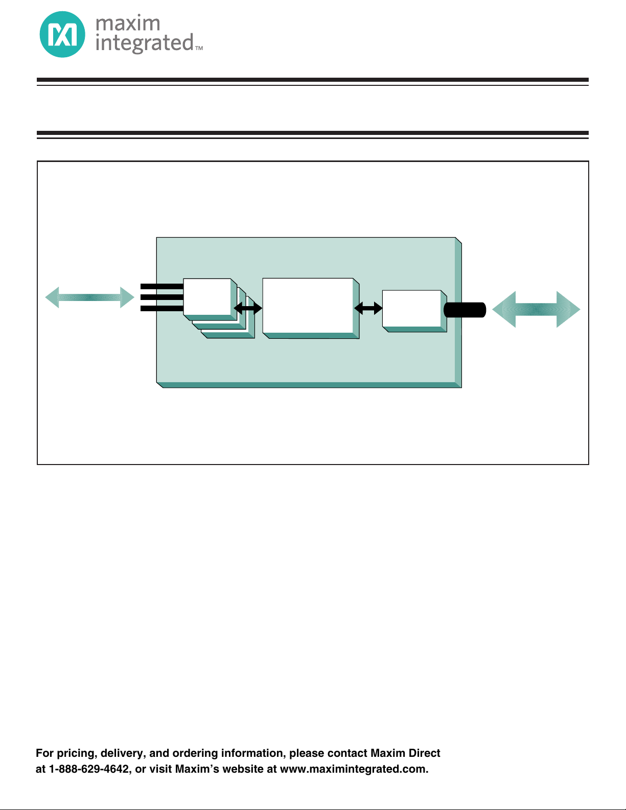
DS80C400/DS80C410/DS80C411
NETWORKED MICROCONTROLLER
HIGH-SPEED MICROCONTROLLER USER’S GUIDE:
NETWORK MICROCONTROLLER SUPPLEMENT
This document is provided as a supplement to the High-Speed Microcontroller User’s Guide, covering new or modified features spe-
cific to the DS80C400/DS80C410/DS80C411. This document must be used in conjunction with the High-Speed
Microcontroller User’s Guide, available from Maxim. Addenda are arranged by section number, which correspond to sections in the High-Speed Microcontroller User’s Guide.
Unless otherwise specified, the references to the DS80C400 and its features also apply to the DS80C410 and DS80C411. Exceptions
include differences in the amount of internal memory and the inclusion/exclusion of the CAN module.
The following additions and changes, with respect to the High-Speed Microcontroller User’s Guide, are contained in this document.
This document is a work in progress, and updates/additions are added when available.
Rev: 12; 9/08
Page 2

High-Speed Microcontroller User’s
Maxim Integrated
Guide: Network Microcontroller
Supplement
TABLE OF CONTENTS
ADDENDUM TO SECTION 1: INTRODUCTION 14
Features . . . . . . . . . . . . . . . . . . . . . . . . . . . . . . . . . . . . . . . . . . . . . . . . . . . . . . . . . . . . . . . . . . .14
ADDENDUM TO SECTION 2: ORDERING INFORMATION 15
Refer to the device-specific data sheet(s) for more information.
ADDENDUM TO SECTION 3: ARCHITECTURE 15
CPU Core and CPU Registers . . . . . . . . . . . . . . . . . . . . . . . . . . . . . . . . . . . . . . . . . . . . . . . . . .15
ADDENDUM TO SECTION 4: PROGRAMMING MODEL 16
Memory Map . . . . . . . . . . . . . . . . . . . . . . . . . . . . . . . . . . . . . . . . . . . . . . . . . . . . . . . . . . . . . . . .16
Register Map . . . . . . . . . . . . . . . . . . . . . . . . . . . . . . . . . . . . . . . . . . . . . . . . . . . . . . . . . . . . . . .17
Bit-Addressable Locations . . . . . . . . . . . . . . . . . . . . . . . . . . . . . . . . . . . . . . . . . . . . . . . . . .17
Working Registers . . . . . . . . . . . . . . . . . . . . . . . . . . . . . . . . . . . . . . . . . . . . . . . . . . . . . . . .17
Stack . . . . . . . . . . . . . . . . . . . . . . . . . . . . . . . . . . . . . . . . . . . . . . . . . . . . . . . . . . . . . . . . . . .17
Special-Function Register Maps . . . . . . . . . . . . . . . . . . . . . . . . . . . . . . . . . . . . . . . . . . . . . . . .17
Special-Function Register Map . . . . . . . . . . . . . . . . . . . . . . . . . . . . . . . . . . . . . . . . . . . . . .18
Special-Function Register Location . . . . . . . . . . . . . . . . . . . . . . . . . . . . . . . . . . . . . . . . . . .18
Special-Function Register Reset Values . . . . . . . . . . . . . . . . . . . . . . . . . . . . . . . . . . . . . . .21
Special-Function Registers . . . . . . . . . . . . . . . . . . . . . . . . . . . . . . . . . . . . . . . . . . . . . . . . . . . . .24
Port 4 (P4) . . . . . . . . . . . . . . . . . . . . . . . . . . . . . . . . . . . . . . . . . . . . . . . . . . . . . . . . . . . . . .24
Stack Pointer (SP) . . . . . . . . . . . . . . . . . . . . . . . . . . . . . . . . . . . . . . . . . . . . . . . . . . . . . . . .25
Data Pointer Low 0 (DPL) . . . . . . . . . . . . . . . . . . . . . . . . . . . . . . . . . . . . . . . . . . . . . . . . . . .25
Data Pointer High 0 (DPH) . . . . . . . . . . . . . . . . . . . . . . . . . . . . . . . . . . . . . . . . . . . . . . . . . .25
Data Pointer Low 1 (DPL1) . . . . . . . . . . . . . . . . . . . . . . . . . . . . . . . . . . . . . . . . . . . . . . . . . .25
Data Pointer High 1 (DPH1) . . . . . . . . . . . . . . . . . . . . . . . . . . . . . . . . . . . . . . . . . . . . . . . . .25
Data Pointer Select (DPS) . . . . . . . . . . . . . . . . . . . . . . . . . . . . . . . . . . . . . . . . . . . . . . . . . .26
Power Control (PCON) . . . . . . . . . . . . . . . . . . . . . . . . . . . . . . . . . . . . . . . . . . . . . . . . . . . . .27
Timer/Counter Control (TCON) . . . . . . . . . . . . . . . . . . . . . . . . . . . . . . . . . . . . . . . . . . . . . . .28
Timer Mode Control (TMOD) . . . . . . . . . . . . . . . . . . . . . . . . . . . . . . . . . . . . . . . . . . . . . . . .29
Timer 0 LSB (TL0) . . . . . . . . . . . . . . . . . . . . . . . . . . . . . . . . . . . . . . . . . . . . . . . . . . . . . . . .30
Timer 1 LSB (TL1) . . . . . . . . . . . . . . . . . . . . . . . . . . . . . . . . . . . . . . . . . . . . . . . . . . . . . . . .30
Timer 0 MSB (TH0) . . . . . . . . . . . . . . . . . . . . . . . . . . . . . . . . . . . . . . . . . . . . . . . . . . . . . . . .30
Timer 1 MSB (TH1) . . . . . . . . . . . . . . . . . . . . . . . . . . . . . . . . . . . . . . . . . . . . . . . . . . . . . . . .30
Clock Control (CKCON) . . . . . . . . . . . . . . . . . . . . . . . . . . . . . . . . . . . . . . . . . . . . . . . . . . . .31
Port 1 (P1) . . . . . . . . . . . . . . . . . . . . . . . . . . . . . . . . . . . . . . . . . . . . . . . . . . . . . . . . . . . . . .32
External Interrupt Flag (EXIF) . . . . . . . . . . . . . . . . . . . . . . . . . . . . . . . . . . . . . . . . . . . . . . . .33
Port 4 Control Register (P4CNT) . . . . . . . . . . . . . . . . . . . . . . . . . . . . . . . . . . . . . . . . . . . . .34
Data Pointer Extended Register 0 (DPX) . . . . . . . . . . . . . . . . . . . . . . . . . . . . . . . . . . . . . . .35
2
Page 3

High-Speed Microcontroller User’s
Maxim Integrated
Guide: Network Microcontroller
Supplement
Data Pointer Extended Register 1 (DPX1) . . . . . . . . . . . . . . . . . . . . . . . . . . . . . . . . . . . . . .35
CAN 0 Receive Message Stored Register 0 (C0RMS0) . . . . . . . . . . . . . . . . . . . . . . . . . . .36
CAN 0 Receive Message Stored Register 1 (C0RMS1) . . . . . . . . . . . . . . . . . . . . . . . . . . .37
Serial Port 0 Control (SCON0) . . . . . . . . . . . . . . . . . . . . . . . . . . . . . . . . . . . . . . . . . . . . . . .38
Serial Data Buffer 0 (SBUF0) . . . . . . . . . . . . . . . . . . . . . . . . . . . . . . . . . . . . . . . . . . . . . . . .38
Extended Stack Pointer Register (ESP) . . . . . . . . . . . . . . . . . . . . . . . . . . . . . . . . . . . . . . . .39
Address Page Register (AP) . . . . . . . . . . . . . . . . . . . . . . . . . . . . . . . . . . . . . . . . . . . . . . . .39
Address Control Register (ACON) . . . . . . . . . . . . . . . . . . . . . . . . . . . . . . . . . . . . . . . . . . . .40
CAN 0 Transmit Message Acknowledgment Register 0 (C0TMA0) . . . . . . . . . . . . . . . . . .41
CAN 0 Transmit Message Acknowledgment Register 1 (C0TMA1) . . . . . . . . . . . . . . . . . .42
Port 2 (P2) . . . . . . . . . . . . . . . . . . . . . . . . . . . . . . . . . . . . . . . . . . . . . . . . . . . . . . . . . . . . . .43
Port 5 (P5) . . . . . . . . . . . . . . . . . . . . . . . . . . . . . . . . . . . . . . . . . . . . . . . . . . . . . . . . . . . . . .43
Port 5 Control Register (P5CNT) . . . . . . . . . . . . . . . . . . . . . . . . . . . . . . . . . . . . . . . . . . . . .44
CAN 0 Control Register (C0C) . . . . . . . . . . . . . . . . . . . . . . . . . . . . . . . . . . . . . . . . . . . . . . .45
CAN 0 Status Register (C0S) . . . . . . . . . . . . . . . . . . . . . . . . . . . . . . . . . . . . . . . . . . . . . . . .48
CAN 0 Interrupt Register (C0IR) . . . . . . . . . . . . . . . . . . . . . . . . . . . . . . . . . . . . . . . . . . . . .51
CAN 0 Receive-Error Register (C0RE) . . . . . . . . . . . . . . . . . . . . . . . . . . . . . . . . . . . . . . . . .54
Interrupt Enable (IE) . . . . . . . . . . . . . . . . . . . . . . . . . . . . . . . . . . . . . . . . . . . . . . . . . . . . . . .55
Slave Address Register 0 (SADDR0) . . . . . . . . . . . . . . . . . . . . . . . . . . . . . . . . . . . . . . . . . .55
Slave Address Register 1 (SADDR1) . . . . . . . . . . . . . . . . . . . . . . . . . . . . . . . . . . . . . . . . . .56
CAN 0 Message Center 1 Control Register (C0M1C) . . . . . . . . . . . . . . . . . . . . . . . . . . . . .56
CAN 0 Message Center 2 Control Register (C0M2C) . . . . . . . . . . . . . . . . . . . . . . . . . . . . .59
CAN 0 Message Center 3 Control Register (C0M3C) . . . . . . . . . . . . . . . . . . . . . . . . . . . . .59
CAN 0 Message Center 4 Control Register (C0M4C) . . . . . . . . . . . . . . . . . . . . . . . . . . . . .59
CAN 0 Message Center 5 Control Register (C0M5C) . . . . . . . . . . . . . . . . . . . . . . . . . . . . .59
Port 3 (P3) . . . . . . . . . . . . . . . . . . . . . . . . . . . . . . . . . . . . . . . . . . . . . . . . . . . . . . . . . . . . . .60
Port 6 (P6) . . . . . . . . . . . . . . . . . . . . . . . . . . . . . . . . . . . . . . . . . . . . . . . . . . . . . . . . . . . . . .61
Port 6 Control Register (P6CNT) . . . . . . . . . . . . . . . . . . . . . . . . . . . . . . . . . . . . . . . . . . . . .62
CAN 0 Message Center 6 Control Register (C0M6C) . . . . . . . . . . . . . . . . . . . . . . . . . . . . .63
CAN 0 Message Center 7 Control Register (C0M7C) . . . . . . . . . . . . . . . . . . . . . . . . . . . . .64
CAN 0 Message Center 8 Control Register (C0M8C) . . . . . . . . . . . . . . . . . . . . . . . . . . . . .64
CAN 0 Message Center 9 Control Register (C0M9C) . . . . . . . . . . . . . . . . . . . . . . . . . . . . .64
CAN 0 Message Center 10 Control Register (C0M10C) . . . . . . . . . . . . . . . . . . . . . . . . . . .64
Interrupt Priority (IP) . . . . . . . . . . . . . . . . . . . . . . . . . . . . . . . . . . . . . . . . . . . . . . . . . . . . . . .65
Slave Address Mask Enable Register 0 (SADEN0) . . . . . . . . . . . . . . . . . . . . . . . . . . . . . . .65
Slave Address Mask Enable Register 1 (SADEN1) . . . . . . . . . . . . . . . . . . . . . . . . . . . . . . .66
CAN 0 Message Center 11 Control Register (C0M11C) . . . . . . . . . . . . . . . . . . . . . . . . . . .66
CAN 0 Message Center 12 Control Register (C0M12C) . . . . . . . . . . . . . . . . . . . . . . . . . . .66
CAN 0 Message Center 13 Control Register (C0M13C) . . . . . . . . . . . . . . . . . . . . . . . . . . .66
CAN 0 Message Center 14 Control Register (C0M14C) . . . . . . . . . . . . . . . . . . . . . . . . . . .67
3
Page 4

High-Speed Microcontroller User’s
Maxim Integrated
Guide: Network Microcontroller
Supplement
CAN 0 Message Center 15 Control Register (C0M15C) . . . . . . . . . . . . . . . . . . . . . . . . . . .67
Serial Port Control (SCON1) . . . . . . . . . . . . . . . . . . . . . . . . . . . . . . . . . . . . . . . . . . . . . . . . .67
Serial Data Buffer 1 (SBUF1) . . . . . . . . . . . . . . . . . . . . . . . . . . . . . . . . . . . . . . . . . . . . . . . .68
Power-Management Register (PMR) . . . . . . . . . . . . . . . . . . . . . . . . . . . . . . . . . . . . . . . . . .68
Status Register (STATUS) . . . . . . . . . . . . . . . . . . . . . . . . . . . . . . . . . . . . . . . . . . . . . . . . . . .70
Memory Control Register (MCON) . . . . . . . . . . . . . . . . . . . . . . . . . . . . . . . . . . . . . . . . . . . .70
Timed-Access Register (TA) . . . . . . . . . . . . . . . . . . . . . . . . . . . . . . . . . . . . . . . . . . . . . . . .71
Timer 2 Control (T2CON) . . . . . . . . . . . . . . . . . . . . . . . . . . . . . . . . . . . . . . . . . . . . . . . . . . .72
Timer 2 Mode (T2MOD) . . . . . . . . . . . . . . . . . . . . . . . . . . . . . . . . . . . . . . . . . . . . . . . . . . . .73
Timer 2 Capture LSB (RCAP2L) . . . . . . . . . . . . . . . . . . . . . . . . . . . . . . . . . . . . . . . . . . . . . .73
Timer 2 Capture MSB (RCAP2H) . . . . . . . . . . . . . . . . . . . . . . . . . . . . . . . . . . . . . . . . . . . . .73
Timer 2 LSB (TL2) . . . . . . . . . . . . . . . . . . . . . . . . . . . . . . . . . . . . . . . . . . . . . . . . . . . . . . . .74
Timer 2 MSB (TH2) . . . . . . . . . . . . . . . . . . . . . . . . . . . . . . . . . . . . . . . . . . . . . . . . . . . . . . . .74
Clock Output Register (COR) . . . . . . . . . . . . . . . . . . . . . . . . . . . . . . . . . . . . . . . . . . . . . . . .74
Program Status Word (PSW) . . . . . . . . . . . . . . . . . . . . . . . . . . . . . . . . . . . . . . . . . . . . . . . .75
Multiplier Control Register 0 (MCNT0) . . . . . . . . . . . . . . . . . . . . . . . . . . . . . . . . . . . . . . . . .76
Multiplier Control Register 1 (MCNT1) . . . . . . . . . . . . . . . . . . . . . . . . . . . . . . . . . . . . . . . . .77
Multiplier A Register (MA) . . . . . . . . . . . . . . . . . . . . . . . . . . . . . . . . . . . . . . . . . . . . . . . . . .77
Multiplier B Register (MB) . . . . . . . . . . . . . . . . . . . . . . . . . . . . . . . . . . . . . . . . . . . . . . . . . .78
Multiplier C Register (MC) . . . . . . . . . . . . . . . . . . . . . . . . . . . . . . . . . . . . . . . . . . . . . . . . . .79
Memory Control Register 1 (MCON1) . . . . . . . . . . . . . . . . . . . . . . . . . . . . . . . . . . . . . . . . .79
Memory Control Register 2 (MCON2) . . . . . . . . . . . . . . . . . . . . . . . . . . . . . . . . . . . . . . . . .81
Watchdog Control (WDCON) . . . . . . . . . . . . . . . . . . . . . . . . . . . . . . . . . . . . . . . . . . . . . . . .82
Slave Address Register 2 (SADDR2) . . . . . . . . . . . . . . . . . . . . . . . . . . . . . . . . . . . . . . . . . .83
Breakpoint Address Register 1 (BPA1) . . . . . . . . . . . . . . . . . . . . . . . . . . . . . . . . . . . . . . . .83
Breakpoint Address Register 2 (BPA2) . . . . . . . . . . . . . . . . . . . . . . . . . . . . . . . . . . . . . . . .83
Breakpoint Address Register 3 (BPA3) . . . . . . . . . . . . . . . . . . . . . . . . . . . . . . . . . . . . . . . .83
Accumulator (AC) . . . . . . . . . . . . . . . . . . . . . . . . . . . . . . . . . . . . . . . . . . . . . . . . . . . . . . . . .84
One’s Complement Adder Data (OCAD) . . . . . . . . . . . . . . . . . . . . . . . . . . . . . . . . . . . . . . .84
CSR Data (CSRD) . . . . . . . . . . . . . . . . . . . . . . . . . . . . . . . . . . . . . . . . . . . . . . . . . . . . . . . .84
CSR Address (CSRA) . . . . . . . . . . . . . . . . . . . . . . . . . . . . . . . . . . . . . . . . . . . . . . . . . . . . . .84
Ethernet Buffer Size (EBS) . . . . . . . . . . . . . . . . . . . . . . . . . . . . . . . . . . . . . . . . . . . . . . . . . .85
Buffer Control Unit Data (BCUD) . . . . . . . . . . . . . . . . . . . . . . . . . . . . . . . . . . . . . . . . . . . . .85
Buffer Control Unit Control (BCUC) . . . . . . . . . . . . . . . . . . . . . . . . . . . . . . . . . . . . . . . . . . .86
Extended Interrupt Enable (EIE) . . . . . . . . . . . . . . . . . . . . . . . . . . . . . . . . . . . . . . . . . . . . .87
MOVX Address Extended Register (MXAX) . . . . . . . . . . . . . . . . . . . . . . . . . . . . . . . . . . . . .87
Data Pointer Extended Register 2 (DPX2) . . . . . . . . . . . . . . . . . . . . . . . . . . . . . . . . . . . . . .88
Data Pointer Extended Register 3 (DPX3) . . . . . . . . . . . . . . . . . . . . . . . . . . . . . . . . . . . . . .88
1-Wire Master Address Register (OWMAD) . . . . . . . . . . . . . . . . . . . . . . . . . . . . . . . . . . . . .88
1-Wire Master Data Register (OWMDR) . . . . . . . . . . . . . . . . . . . . . . . . . . . . . . . . . . . . . . . .89
4
Page 5

High-Speed Microcontroller User’s
Maxim Integrated
Guide: Network Microcontroller
Supplement
B Register (B) . . . . . . . . . . . . . . . . . . . . . . . . . . . . . . . . . . . . . . . . . . . . . . . . . . . . . . . . . . . .89
Slave Address Mask Enable Register 2 (SADEN2) . . . . . . . . . . . . . . . . . . . . . . . . . . . . . . .89
Data Pointer Low Register 2 (DPL2) . . . . . . . . . . . . . . . . . . . . . . . . . . . . . . . . . . . . . . . . . .89
Data Pointer High Register 2 (DPH2) . . . . . . . . . . . . . . . . . . . . . . . . . . . . . . . . . . . . . . . . . .90
Data Pointer Low Register 3 (DPL3) . . . . . . . . . . . . . . . . . . . . . . . . . . . . . . . . . . . . . . . . . .90
Data Pointer High Register 3 (DPH3) . . . . . . . . . . . . . . . . . . . . . . . . . . . . . . . . . . . . . . . . . .90
Data Pointer Select Register 1 (DPS1) . . . . . . . . . . . . . . . . . . . . . . . . . . . . . . . . . . . . . . . . .90
Status Register 1 (STATUS1) . . . . . . . . . . . . . . . . . . . . . . . . . . . . . . . . . . . . . . . . . . . . . . . .91
Extended Interrupt Priority (EIP) . . . . . . . . . . . . . . . . . . . . . . . . . . . . . . . . . . . . . . . . . . . . . .91
Parallel I/O Port (P7) . . . . . . . . . . . . . . . . . . . . . . . . . . . . . . . . . . . . . . . . . . . . . . . . . . . . . . .92
Timer 3 LSB (TL3) . . . . . . . . . . . . . . . . . . . . . . . . . . . . . . . . . . . . . . . . . . . . . . . . . . . . . . . .92
Timer 3 MSB (TH3) . . . . . . . . . . . . . . . . . . . . . . . . . . . . . . . . . . . . . . . . . . . . . . . . . . . . . . . .92
Timer 3 Control/Mode Register (T3CM) . . . . . . . . . . . . . . . . . . . . . . . . . . . . . . . . . . . . . . . .93
Serial Port 2 Control Register (SCON2) . . . . . . . . . . . . . . . . . . . . . . . . . . . . . . . . . . . . . . . .94
Serial Data Buffer 2 (SBUF2) . . . . . . . . . . . . . . . . . . . . . . . . . . . . . . . . . . . . . . . . . . . . . . . .94
ADDENDUM TO SECTION 5: CPU TIMING 95
External Clock Source . . . . . . . . . . . . . . . . . . . . . . . . . . . . . . . . . . . . . . . . . . . . . . . . . . . . . . . .95
System Clock Selection . . . . . . . . . . . . . . . . . . . . . . . . . . . . . . . . . . . . . . . . . . . . . . . . . . . . . . .95
Changing the System Clock/Machine Cycle Clock Frequency . . . . . . . . . . . . . . . . . . . . . . . . .96
ADDENDUM TO SECTION 6: MEMORY ACCESS 97
Internal Program Memory . . . . . . . . . . . . . . . . . . . . . . . . . . . . . . . . . . . . . . . . . . . . . . . . . . . . . .97
Internal Data Memory . . . . . . . . . . . . . . . . . . . . . . . . . . . . . . . . . . . . . . . . . . . . . . . . . . . . . . . . .98
DS80C400 . . . . . . . . . . . . . . . . . . . . . . . . . . . . . . . . . . . . . . . . . . . . . . . . . . . . . . . . . . . . . .98
DS80C410/DS80C411 . . . . . . . . . . . . . . . . . . . . . . . . . . . . . . . . . . . . . . . . . . . . . . . . . . . . .99
External Memory Access . . . . . . . . . . . . . . . . . . . . . . . . . . . . . . . . . . . . . . . . . . . . . . . . . . . . . .100
Using the Combined Chip-Enable Signals . . . . . . . . . . . . . . . . . . . . . . . . . . . . . . . . . . . . . . . . .104
Write-Protection Feature (DS80C400 Only) . . . . . . . . . . . . . . . . . . . . . . . . . . . . . . . . . . . . . . . .108
Enhanced Quad Data Pointers . . . . . . . . . . . . . . . . . . . . . . . . . . . . . . . . . . . . . . . . . . . . . . . . . .108
ADDENDUM TO SECTION 7: POWER MANAGEMENT 109
Precision Voltage Monitor . . . . . . . . . . . . . . . . . . . . . . . . . . . . . . . . . . . . . . . . . . . . . . . . . . . . . .109
Early Warning Power-Fail Interrupt . . . . . . . . . . . . . . . . . . . . . . . . . . . . . . . . . . . . . . . . . . . . . . .110
Power-Fail Reset . . . . . . . . . . . . . . . . . . . . . . . . . . . . . . . . . . . . . . . . . . . . . . . . . . . . . . . . . . . . .110
Power-On Reset . . . . . . . . . . . . . . . . . . . . . . . . . . . . . . . . . . . . . . . . . . . . . . . . . . . . . . . . . . . . .110
Bandgap Select . . . . . . . . . . . . . . . . . . . . . . . . . . . . . . . . . . . . . . . . . . . . . . . . . . . . . . . . . . . . .110
Power-Management Summary . . . . . . . . . . . . . . . . . . . . . . . . . . . . . . . . . . . . . . . . . . . . . . . . . .110
Power-Management Modes . . . . . . . . . . . . . . . . . . . . . . . . . . . . . . . . . . . . . . . . . . . . . . . . . . . .110
PMM and Peripheral Functions . . . . . . . . . . . . . . . . . . . . . . . . . . . . . . . . . . . . . . . . . . . . . . . . .110
Switchback . . . . . . . . . . . . . . . . . . . . . . . . . . . . . . . . . . . . . . . . . . . . . . . . . . . . . . . . . . . . . . . . .111
5
Page 6

High-Speed Microcontroller User’s
Maxim Integrated
Guide: Network Microcontroller
Supplement
Stop Mode . . . . . . . . . . . . . . . . . . . . . . . . . . . . . . . . . . . . . . . . . . . . . . . . . . . . . . . . . . . . . . . . .111
Pin States in Idle or Stop Mode . . . . . . . . . . . . . . . . . . . . . . . . . . . . . . . . . . . . . . . . . . . . . . . . .111
Switching Between Clock Sources . . . . . . . . . . . . . . . . . . . . . . . . . . . . . . . . . . . . . . . . . . . . . . .111
ADDENDUM TO SECTION 8: RESET CONDITIONS 111
Reset Sources . . . . . . . . . . . . . . . . . . . . . . . . . . . . . . . . . . . . . . . . . . . . . . . . . . . . . . . . . . . . . . .111
Power-On/Power-Fail Reset . . . . . . . . . . . . . . . . . . . . . . . . . . . . . . . . . . . . . . . . . . . . . . . . .112
Watchdog Timer Reset . . . . . . . . . . . . . . . . . . . . . . . . . . . . . . . . . . . . . . . . . . . . . . . . . . . . .112
External Reset . . . . . . . . . . . . . . . . . . . . . . . . . . . . . . . . . . . . . . . . . . . . . . . . . . . . . . . . . . .112
Oscillator Fail-Detect Reset . . . . . . . . . . . . . . . . . . . . . . . . . . . . . . . . . . . . . . . . . . . . . . . . .112
Reset Outputs . . . . . . . . . . . . . . . . . . . . . . . . . . . . . . . . . . . . . . . . . . . . . . . . . . . . . . . . . . . . . . .113
Reset Output Low (RSTOL) . . . . . . . . . . . . . . . . . . . . . . . . . . . . . . . . . . . . . . . . . . . . . . . . .113
Reset State . . . . . . . . . . . . . . . . . . . . . . . . . . . . . . . . . . . . . . . . . . . . . . . . . . . . . . . . . . . . . . . . .113
In-System Disable Mode . . . . . . . . . . . . . . . . . . . . . . . . . . . . . . . . . . . . . . . . . . . . . . . . . . . . . .113
ADDENDUM TO SECTION 9: INTERRUPTS 114
ADDENDUM TO SECTION 10: PARALLEL I/O 116
Port 0 . . . . . . . . . . . . . . . . . . . . . . . . . . . . . . . . . . . . . . . . . . . . . . . . . . . . . . . . . . . . . . . . . . . . .116
Ports 4–7 . . . . . . . . . . . . . . . . . . . . . . . . . . . . . . . . . . . . . . . . . . . . . . . . . . . . . . . . . . . . . . . . . . .116
General-Purpose I/O . . . . . . . . . . . . . . . . . . . . . . . . . . . . . . . . . . . . . . . . . . . . . . . . . . . . . . . . . .116
Alternate Functions A0–A7, A16–A21, CE0–7, and PCE0–3 . . . . . . . . . . . . . . . . . . . . . . . . . . .116
Current-Limited Transitions . . . . . . . . . . . . . . . . . . . . . . . . . . . . . . . . . . . . . . . . . . . . . . . . . . . . .116
5V-Tolerant I/O . . . . . . . . . . . . . . . . . . . . . . . . . . . . . . . . . . . . . . . . . . . . . . . . . . . . . . . . . . . . . .117
ADDENDUM TO SECTION 11: PROGRAMMABLE TIMERS 118
Divide-by-13 Option . . . . . . . . . . . . . . . . . . . . . . . . . . . . . . . . . . . . . . . . . . . . . . . . . . . . . . . . . .122
Programmable Clock Output . . . . . . . . . . . . . . . . . . . . . . . . . . . . . . . . . . . . . . . . . . . . . . . . . . .123
IrDA Clock Output . . . . . . . . . . . . . . . . . . . . . . . . . . . . . . . . . . . . . . . . . . . . . . . . . . . . . . . . . . .123
ADDENDUM TO SECTION 12: SERIAL I/O 124
Serial Mode Summary . . . . . . . . . . . . . . . . . . . . . . . . . . . . . . . . . . . . . . . . . . . . . . . . . . . . . . . .124
Baud Rates . . . . . . . . . . . . . . . . . . . . . . . . . . . . . . . . . . . . . . . . . . . . . . . . . . . . . . . . . . . . . . . . .124
Mode 0 . . . . . . . . . . . . . . . . . . . . . . . . . . . . . . . . . . . . . . . . . . . . . . . . . . . . . . . . . . . . . . . . .125
Mode 2 . . . . . . . . . . . . . . . . . . . . . . . . . . . . . . . . . . . . . . . . . . . . . . . . . . . . . . . . . . . . . . . . .126
Mode 1 or 3 . . . . . . . . . . . . . . . . . . . . . . . . . . . . . . . . . . . . . . . . . . . . . . . . . . . . . . . . . . . . .126
Using Timer 1 or Timer 3 for Baud-Rate Generation . . . . . . . . . . . . . . . . . . . . . . . . . . . . . .127
Using Timer 2 for Baud-Rate Generation . . . . . . . . . . . . . . . . . . . . . . . . . . . . . . . . . . . . . . .127
ADDENDUM TO SECTION 13: TIMED-ACCESS PROTECTION 129
ADDENDUM TO SECTION 14: REAL-TIME CLOCK 129
Refer to the High-Speed Microcontroller User’s Guide. Not applicable to the DS80C400/410/411.
6
Page 7

High-Speed Microcontroller User’s
Maxim Integrated
Guide: Network Microcontroller
Supplement
ADDENDUM TO SECTION 15: BATTERY BACKUP 129
Refer to the High-Speed Microcontroller User’s Guide. Not applicable to the DS80C400/410/411.
ADDENDUM TO SECTION 16: INSTRUCTION SET DETAILS 130
16-Bit (8051 Standard) Addressing Mode . . . . . . . . . . . . . . . . . . . . . . . . . . . . . . . . . . . . . . . . .130
24-Bit Paged Addressing Mode . . . . . . . . . . . . . . . . . . . . . . . . . . . . . . . . . . . . . . . . . . . . . . . . .130
24-Bit Contiguous Addressing Mode . . . . . . . . . . . . . . . . . . . . . . . . . . . . . . . . . . . . . . . . . . . . .132
ADDENDUM TO SECTION 17: TROUBLESHOOTING 133
Software Breakpoint Mode . . . . . . . . . . . . . . . . . . . . . . . . . . . . . . . . . . . . . . . . . . . . . . . . . . . . .133
Generating a Breakpoint . . . . . . . . . . . . . . . . . . . . . . . . . . . . . . . . . . . . . . . . . . . . . . . . . . . . . .133
Exiting a Breakpoint . . . . . . . . . . . . . . . . . . . . . . . . . . . . . . . . . . . . . . . . . . . . . . . . . . . . . . . . . .133
ADDENDUM TO SECTION 18: MICROCONTROLLER
DEVELOPMENT SUPPORT 135
Refer to the High-Speed Microcontroller User’s Guide.
SECTION 19: CONTROLLER AREA NETWORK (CAN) MODULE 136
MOVX Message Centers for CAN 0 . . . . . . . . . . . . . . . . . . . . . . . . . . . . . . . . . . . . . . . . . . . . . .137
CAN MOVX Register Description . . . . . . . . . . . . . . . . . . . . . . . . . . . . . . . . . . . . . . . . . . . . . . . .138
CAN 0 Media ID Mask Register 0 (COMID0) . . . . . . . . . . . . . . . . . . . . . . . . . . . . . . . . . . .139
CAN 0 Media ID Mask Register 1 (COMID1) . . . . . . . . . . . . . . . . . . . . . . . . . . . . . . . . . . .139
CAN 0 Media Arbitration Register 0 (C0MA0) . . . . . . . . . . . . . . . . . . . . . . . . . . . . . . . . . . .139
CAN 0 Media Arbitration Register 1 (C0MA1) . . . . . . . . . . . . . . . . . . . . . . . . . . . . . . . . . . .139
CAN 0 Bus Timing Register 0 (C0BT0) . . . . . . . . . . . . . . . . . . . . . . . . . . . . . . . . . . . . . . . .140
CAN 0 Bus Timing Register 1 (C0BT1) . . . . . . . . . . . . . . . . . . . . . . . . . . . . . . . . . . . . . . . .141
CAN 0 Standard Global Mask Register 0 (C0SGM0) . . . . . . . . . . . . . . . . . . . . . . . . . . . . .142
CAN 0 Standard Global Mask Register 1 (C0SGM1) . . . . . . . . . . . . . . . . . . . . . . . . . . . . .142
CAN 0 Extended Global Mask Register 0 (C0EGM0) . . . . . . . . . . . . . . . . . . . . . . . . . . . . .142
CAN 0 Extended Global Mask Register 1 (C0EGM1) . . . . . . . . . . . . . . . . . . . . . . . . . . . . .142
CAN 0 Extended Global Mask Register 2 (C0EGM2) . . . . . . . . . . . . . . . . . . . . . . . . . . . . .142
CAN 0 Extended Global Mask Register 3 (C0EGM3) . . . . . . . . . . . . . . . . . . . . . . . . . . . . .143
CAN 0 Message Center 15 Mask Register 0 (C0M15M0) . . . . . . . . . . . . . . . . . . . . . . . . . .143
CAN 0 Message Center 15 Mask Register 1 (C0M15M1) . . . . . . . . . . . . . . . . . . . . . . . . . .143
CAN 0 Message Center 15 Mask Register 2 (C0M15M2) . . . . . . . . . . . . . . . . . . . . . . . . . .143
CAN 0 Message Center 15 Mask Register 3 (C0M15M3) . . . . . . . . . . . . . . . . . . . . . . . . . .144
CAN Message Center MOVX Register Descriptions . . . . . . . . . . . . . . . . . . . . . . . . . . . . . . . . .144
CAN 0 Message Center y Arbitration Register 0 (C0MyAR0) . . . . . . . . . . . . . . . . . . . . . . .144
CAN 0 Message Center y Arbitration Register 1 (C0MyAR1) . . . . . . . . . . . . . . . . . . . . . . .144
CAN 0 Message Center y Arbitration Register 2 (C0MyAR2) . . . . . . . . . . . . . . . . . . . . . . .144
CAN 0 Message Center y Arbitration Register 3 (C0MyAR3) . . . . . . . . . . . . . . . . . . . . . . .145
7
Page 8

High-Speed Microcontroller User’s
Maxim Integrated
Guide: Network Microcontroller
Supplement
CAN 0 Message Center y Format Register (C0MyF) . . . . . . . . . . . . . . . . . . . . . . . . . . . . . .146
CAN 0 Message Center y Data Byte 0 (C0MyD0) . . . . . . . . . . . . . . . . . . . . . . . . . . . . . . . .147
CAN 0 Message Center y Data Byte 1 (C0MyD1) . . . . . . . . . . . . . . . . . . . . . . . . . . . . . . . .147
CAN 0 Message Center y Data Byte 2 (C0MyD2) . . . . . . . . . . . . . . . . . . . . . . . . . . . . . . . .147
CAN 0 Message Center y Data Byte 3 (C0MyD3) . . . . . . . . . . . . . . . . . . . . . . . . . . . . . . . .147
CAN 0 Message Center y Data Byte 4 (C0MyD4) . . . . . . . . . . . . . . . . . . . . . . . . . . . . . . . .147
CAN 0 Message Center y Data Byte 5 (C0MyD5) . . . . . . . . . . . . . . . . . . . . . . . . . . . . . . . .147
CAN 0 Message Center y Data Byte 6 (C0MyD6) . . . . . . . . . . . . . . . . . . . . . . . . . . . . . . . .147
CAN 0 Message Center y Data Byte 7 (C0MyD7) . . . . . . . . . . . . . . . . . . . . . . . . . . . . . . . .147
Frame Types . . . . . . . . . . . . . . . . . . . . . . . . . . . . . . . . . . . . . . . . . . . . . . . . . . . . . . . . . . . . . . . .148
Initializing the CAN Controller . . . . . . . . . . . . . . . . . . . . . . . . . . . . . . . . . . . . . . . . . . . . . . . . . . .152
CAN Interrupts . . . . . . . . . . . . . . . . . . . . . . . . . . . . . . . . . . . . . . . . . . . . . . . . . . . . . . . . . . . . . .152
Arbitration/Masking Considerations . . . . . . . . . . . . . . . . . . . . . . . . . . . . . . . . . . . . . . . . . . . . . .153
Message Center 15 . . . . . . . . . . . . . . . . . . . . . . . . . . . . . . . . . . . . . . . . . . . . . . . . . . . . . . . . . .154
Transmitting and Receiving Messages . . . . . . . . . . . . . . . . . . . . . . . . . . . . . . . . . . . . . . . .154
Transmitting Data Messages . . . . . . . . . . . . . . . . . . . . . . . . . . . . . . . . . . . . . . . . . . . . . . . .154
Receiving Data Messages . . . . . . . . . . . . . . . . . . . . . . . . . . . . . . . . . . . . . . . . . . . . . . . . . .155
Transmitting Remote Frame Requests . . . . . . . . . . . . . . . . . . . . . . . . . . . . . . . . . . . . . . . . .155
Receiving/Responding to Remote Frame Requests . . . . . . . . . . . . . . . . . . . . . . . . . . . . . .155
Remote Frame Handling in Relation to the DTBYC Bits . . . . . . . . . . . . . . . . . . . . . . . . . . . . . .158
Overwrite Enable/Disable Feature . . . . . . . . . . . . . . . . . . . . . . . . . . . . . . . . . . . . . . . . . . . . . . .158
Case 1: WTOE = 1 (Overwrites allowed) . . . . . . . . . . . . . . . . . . . . . . . . . . . . . . . . . . . . . . .159
Case 2: WTOE = 0 (Overwrites disabled) . . . . . . . . . . . . . . . . . . . . . . . . . . . . . . . . . . . . . .159
Special Considerations for Message Center 15 . . . . . . . . . . . . . . . . . . . . . . . . . . . . . . . . . . . .159
Using the Autobaud Feature . . . . . . . . . . . . . . . . . . . . . . . . . . . . . . . . . . . . . . . . . . . . . . . . . . .159
Bus-Off/Bus-Off Recovery and Error Counter Operation . . . . . . . . . . . . . . . . . . . . . . . . . . . . . .161
Bit Timing . . . . . . . . . . . . . . . . . . . . . . . . . . . . . . . . . . . . . . . . . . . . . . . . . . . . . . . . . . . . . . . . . .162
Threefold Bit Sampling . . . . . . . . . . . . . . . . . . . . . . . . . . . . . . . . . . . . . . . . . . . . . . . . . . . . . . . .163
Bus Rate Timing Example . . . . . . . . . . . . . . . . . . . . . . . . . . . . . . . . . . . . . . . . . . . . . . . . . . . . .164
Additional Bit Timing Examples . . . . . . . . . . . . . . . . . . . . . . . . . . . . . . . . . . . . . . . . . . . . . . . . .164
SECTION 20: ARITHMETIC ACCELERATOR 165
SECTION 21: 1-WIRE BUS MASTER 168
Divide (32-bit by 16-bit or 16-bit by 16-bit) . . . . . . . . . . . . . . . . . . . . . . . . . . . . . . . . . . . . . . . .166
Multiply (16-bit by 16-bit) . . . . . . . . . . . . . . . . . . . . . . . . . . . . . . . . . . . . . . . . . . . . . . . . . . . . . .166
Shift right/left . . . . . . . . . . . . . . . . . . . . . . . . . . . . . . . . . . . . . . . . . . . . . . . . . . . . . . . . . . . . . . . .166
Normalize . . . . . . . . . . . . . . . . . . . . . . . . . . . . . . . . . . . . . . . . . . . . . . . . . . . . . . . . . . . . . . . . . .167
40-Bit Accumulator . . . . . . . . . . . . . . . . . . . . . . . . . . . . . . . . . . . . . . . . . . . . . . . . . . . . . . . . . . .167
Hardware Setup . . . . . . . . . . . . . . . . . . . . . . . . . . . . . . . . . . . . . . . . . . . . . . . . . . . . . . . . . . . . .168
8
Page 9

High-Speed Microcontroller User’s
Maxim Integrated
Guide: Network Microcontroller
Supplement
Setting Up and Using the 1-Wire Master . . . . . . . . . . . . . . . . . . . . . . . . . . . . . . . . . . . . . . . . . .168
Setting Up the 1-Wire Master . . . . . . . . . . . . . . . . . . . . . . . . . . . . . . . . . . . . . . . . . . . . . . . .169
Sending a 1-Wire Reset . . . . . . . . . . . . . . . . . . . . . . . . . . . . . . . . . . . . . . . . . . . . . . . . . . . .169
Sending a Byte . . . . . . . . . . . . . . . . . . . . . . . . . . . . . . . . . . . . . . . . . . . . . . . . . . . . . . . . . . .169
Search ROM Accelerator . . . . . . . . . . . . . . . . . . . . . . . . . . . . . . . . . . . . . . . . . . . . . . . . . . . . . .170
Accelerated ROM Search Example . . . . . . . . . . . . . . . . . . . . . . . . . . . . . . . . . . . . . . . . . . . . . .171
SECTION 22: ETHERNET CONTROLLER 172
Assigning a Physical MAC Address . . . . . . . . . . . . . . . . . . . . . . . . . . . . . . . . . . . . . . . . . . . . . .173
Configuring the MAC Operational Mode . . . . . . . . . . . . . . . . . . . . . . . . . . . . . . . . . . . . . . . . . .173
Media Independent Interface (MII) . . . . . . . . . . . . . . . . . . . . . . . . . . . . . . . . . . . . . . . . . . . . . .174
ENDEC Operation . . . . . . . . . . . . . . . . . . . . . . . . . . . . . . . . . . . . . . . . . . . . . . . . . . . . . . . . . . . .175
ENDEC Mode—Heartbeat Signal Quality Generator . . . . . . . . . . . . . . . . . . . . . . . . . . . . . . . . .176
MAC Primary Functions—Packet Filtering . . . . . . . . . . . . . . . . . . . . . . . . . . . . . . . . . . . . . . . . .176
Using the MII Serial Management Bus . . . . . . . . . . . . . . . . . . . . . . . . . . . . . . . . . . . . . . . . . . . .177
Half-Duplex Operation—CSMA/CD and Flow Control . . . . . . . . . . . . . . . . . . . . . . . . . . . . . . . .177
Deferral Check . . . . . . . . . . . . . . . . . . . . . . . . . . . . . . . . . . . . . . . . . . . . . . . . . . . . . . . . . . . . . .178
Disable Retry . . . . . . . . . . . . . . . . . . . . . . . . . . . . . . . . . . . . . . . . . . . . . . . . . . . . . . . . . . . . . . .178
Back-Off Limit . . . . . . . . . . . . . . . . . . . . . . . . . . . . . . . . . . . . . . . . . . . . . . . . . . . . . . . . . . . . . . .178
Late Collision Control . . . . . . . . . . . . . . . . . . . . . . . . . . . . . . . . . . . . . . . . . . . . . . . . . . . . . . . . .178
Flow Control . . . . . . . . . . . . . . . . . . . . . . . . . . . . . . . . . . . . . . . . . . . . . . . . . . . . . . . . . . . . . . . .179
Full-Duplex Operation . . . . . . . . . . . . . . . . . . . . . . . . . . . . . . . . . . . . . . . . . . . . . . . . . . . . . . . . .179
Pause Control Frame . . . . . . . . . . . . . . . . . . . . . . . . . . . . . . . . . . . . . . . . . . . . . . . . . . . . . . . . .179
Loopback Modes . . . . . . . . . . . . . . . . . . . . . . . . . . . . . . . . . . . . . . . . . . . . . . . . . . . . . . . . . . . .180
Address Filtering Control . . . . . . . . . . . . . . . . . . . . . . . . . . . . . . . . . . . . . . . . . . . . . . . . . . . . . .181
Using the Hash Table . . . . . . . . . . . . . . . . . . . . . . . . . . . . . . . . . . . . . . . . . . . . . . . . . . . . . . . . .182
VLAN Support . . . . . . . . . . . . . . . . . . . . . . . . . . . . . . . . . . . . . . . . . . . . . . . . . . . . . . . . . . . . . . .182
Partitioning the 8kB Ethernet Data Buffer Memory . . . . . . . . . . . . . . . . . . . . . . . . . . . . . . . . . .182
Transmit/Receive Data Buffer Word Orientation: Edianess . . . . . . . . . . . . . . . . . . . . . . . . . . . .184
Transmitting Data . . . . . . . . . . . . . . . . . . . . . . . . . . . . . . . . . . . . . . . . . . . . . . . . . . . . . . . . .184
Receiving Data . . . . . . . . . . . . . . . . . . . . . . . . . . . . . . . . . . . . . . . . . . . . . . . . . . . . . . . . . . .186
Using Wake-Up Frames . . . . . . . . . . . . . . . . . . . . . . . . . . . . . . . . . . . . . . . . . . . . . . . . . . . . . . .187
Magic Packet Mode . . . . . . . . . . . . . . . . . . . . . . . . . . . . . . . . . . . . . . . . . . . . . . . . . . . . . . .187
Network Wake-Up Frame . . . . . . . . . . . . . . . . . . . . . . . . . . . . . . . . . . . . . . . . . . . . . . . . . . .187
SECTION 23: EMBEDDED DS80C400 SILICON SOFTWARE 189
9
Serial Loader . . . . . . . . . . . . . . . . . . . . . . . . . . . . . . . . . . . . . . . . . . . . . . . . . . . . . . . . . . . . . . .189
Autobaud-Rate Detection . . . . . . . . . . . . . . . . . . . . . . . . . . . . . . . . . . . . . . . . . . . . . . . . . . . . . .189
Command Line Interface . . . . . . . . . . . . . . . . . . . . . . . . . . . . . . . . . . . . . . . . . . . . . . . . . . . . . .189
Command Summary . . . . . . . . . . . . . . . . . . . . . . . . . . . . . . . . . . . . . . . . . . . . . . . . . . . . . . . . . .189
Page 10

High-Speed Microcontroller User’s
Maxim Integrated
Guide: Network Microcontroller
Supplement
Exported RAM Functions . . . . . . . . . . . . . . . . . . . . . . . . . . . . . . . . . . . . . . . . . . . . . . . . . . . . . .190
Utility Functions . . . . . . . . . . . . . . . . . . . . . . . . . . . . . . . . . . . . . . . . . . . . . . . . . . . . . . . . . . . . .191
Memory Manager Functions . . . . . . . . . . . . . . . . . . . . . . . . . . . . . . . . . . . . . . . . . . . . . . . . . . . .193
Socket Function Calling Conventions . . . . . . . . . . . . . . . . . . . . . . . . . . . . . . . . . . . . . . . . . . . . .195
Input Parameter Buffer . . . . . . . . . . . . . . . . . . . . . . . . . . . . . . . . . . . . . . . . . . . . . . . . . . . . .195
Output Return Values . . . . . . . . . . . . . . . . . . . . . . . . . . . . . . . . . . . . . . . . . . . . . . . . . . . . . .195
Socket Functions/Pointers . . . . . . . . . . . . . . . . . . . . . . . . . . . . . . . . . . . . . . . . . . . . . . . . . . . . .196
PARAMBUFFER . . . . . . . . . . . . . . . . . . . . . . . . . . . . . . . . . . . . . . . . . . . . . . . . . . . . . . . . . .196
DHCP Functions . . . . . . . . . . . . . . . . . . . . . . . . . . . . . . . . . . . . . . . . . . . . . . . . . . . . . . . . . . . . .203
TFTP Functions/Pointers . . . . . . . . . . . . . . . . . . . . . . . . . . . . . . . . . . . . . . . . . . . . . . . . . . . . . . .204
Task Scheduler Functions . . . . . . . . . . . . . . . . . . . . . . . . . . . . . . . . . . . . . . . . . . . . . . . . . . . . . .205
Task Scheduler User Hooks . . . . . . . . . . . . . . . . . . . . . . . . . . . . . . . . . . . . . . . . . . . . . . . . . . . .208
1-Wire Master . . . . . . . . . . . . . . . . . . . . . . . . . . . . . . . . . . . . . . . . . . . . . . . . . . . . . . . . . . . . . . .209
Additional Functions Available in ROM Version 1.2.0 . . . . . . . . . . . . . . . . . . . . . . . . . . . . . . . .210
Initialization Functions . . . . . . . . . . . . . . . . . . . . . . . . . . . . . . . . . . . . . . . . . . . . . . . . . . . . . . . .214
Asynchronous TCP/IP Maintenance Functions . . . . . . . . . . . . . . . . . . . . . . . . . . . . . . . . . . . . .216
ROM Redirect Function Table . . . . . . . . . . . . . . . . . . . . . . . . . . . . . . . . . . . . . . . . . . . . . . . . . . .217
ROM Redirect Functions . . . . . . . . . . . . . . . . . . . . . . . . . . . . . . . . . . . . . . . . . . . . . . . . . . . . . .218
Timeslice and Task Scheduler Timing . . . . . . . . . . . . . . . . . . . . . . . . . . . . . . . . . . . . . . . . . . . .220
REVISION HISTORY 221
10
Page 11

High-Speed Microcontroller User’s
Maxim Integrated
Guide: Network Microcontroller
Supplement
LIST OF FIGURES
Figure 5-1. System Clock Control Diagram . . . . . . . . . . . . . . . . . . . . . . . . . . . . . . . . . . . . . . . . . . .95
Figure 6-1. Program Memory Map Options . . . . . . . . . . . . . . . . . . . . . . . . . . . . . . . . . . . . . . . . . . .97
Figure 6-2. Example Data Memory Map Configurations (DS80C400) . . . . . . . . . . . . . . . . . . . . . . .98
Figure 6-3. Example Data Memory Map Configurations (DS80C400/DS80C411) . . . . . . . . . . . . . .99
Figure 6-4. Multiplexed Address/Data Bus . . . . . . . . . . . . . . . . . . . . . . . . . . . . . . . . . . . . . . . . . . .103
Figure 6-5. Demultiplexed Address/Data Bus . . . . . . . . . . . . . . . . . . . . . . . . . . . . . . . . . . . . . . . . .104
Figure 6-6. Merged Program/Data Access Under CE0, CE2, PCE0–PCE3
Becomes Inaccessible . . . . . . . . . . . . . . . . . . . . . . . . . . . . . . . . . . . . . . . . . . . . . . . . . .105
Figure 6-7. Merged Program/Data Access Under CE2, CE3, PCE2, and PCE3
Becomes Inaccessible . . . . . . . . . . . . . . . . . . . . . . . . . . . . . . . . . . . . . . . . . . . . . . . . . .106
Figure 6-8. Merged Program/Data Access Under CE1, CE2, PCE1, and PCE2
Becomes Inaccessible . . . . . . . . . . . . . . . . . . . . . . . . . . . . . . . . . . . . . . . . . . . . . . . . . .106
Figure 6-9. Merged Program/Data Access Under CE0 and PCE0 Becomes
Partially Inaccessible . . . . . . . . . . . . . . . . . . . . . . . . . . . . . . . . . . . . . . . . . . . . . . . . . . .107
Figure 6-10. Full 16MB Program/Data Memory Map Options . . . . . . . . . . . . . . . . . . . . . . . . . . . . .107
Figure 9-1. 1-Wire Interrupt Source . . . . . . . . . . . . . . . . . . . . . . . . . . . . . . . . . . . . . . . . . . . . . . . . .114
Figure 9-2. Interrupt Functional Diagram . . . . . . . . . . . . . . . . . . . . . . . . . . . . . . . . . . . . . . . . . . . . .115
Figure 10-1. 5V-Tolerant I/O Pad . . . . . . . . . . . . . . . . . . . . . . . . . . . . . . . . . . . . . . . . . . . . . . . . . . .117
Figure 11-1. Timers/Counters 0, 1, and 3, Modes 0 and 1 . . . . . . . . . . . . . . . . . . . . . . . . . . . . . . .118
Figure 11-2. Timers/Counters 0, 1, and 3, Mode 2 . . . . . . . . . . . . . . . . . . . . . . . . . . . . . . . . . . . . .119
Figure 11-3. Timer/Counter 0, Mode 3 . . . . . . . . . . . . . . . . . . . . . . . . . . . . . . . . . . . . . . . . . . . . . . .119
Figure 11-4. Timer/Counter 2 Clock-Out Mode . . . . . . . . . . . . . . . . . . . . . . . . . . . . . . . . . . . . . . . .120
Figure 11-5. Timer/Counter 2 Baud-Rate Generator Mode . . . . . . . . . . . . . . . . . . . . . . . . . . . . . . .120
Figure 11-6. Timer/Counter 2 Autoreload Mode, DCEN = 0 . . . . . . . . . . . . . . . . . . . . . . . . . . . . . .121
Figure 11-7. Timer/Counter 2 Autoreload Mode, DCEN = 1 . . . . . . . . . . . . . . . . . . . . . . . . . . . . . .121
Figure 11-8. Timer/Counter 2 with Optional Capture . . . . . . . . . . . . . . . . . . . . . . . . . . . . . . . . . . . .122
Figure 11-9. Operation of Divide-by-13 Bits . . . . . . . . . . . . . . . . . . . . . . . . . . . . . . . . . . . . . . . . . . .122
Figure 11-10. Sample IrDA Implementation . . . . . . . . . . . . . . . . . . . . . . . . . . . . . . . . . . . . . . . . . . .123
Figure 12-1. Serial Port Mode 0 Block Diagram Change . . . . . . . . . . . . . . . . . . . . . . . . . . . . . . . . .125
Figure 12-2. Serial Port Mode 2 Block Diagram Change . . . . . . . . . . . . . . . . . . . . . . . . . . . . . . . . .126
Figure 12-3. Serial Port Modes 1, 3 Block Diagram Change . . . . . . . . . . . . . . . . . . . . . . . . . . . . . .128
Figure 17-1. Force Feeding a Breakpoint During An Instruction Other Than MOVC or MOVX . . . .134
Figure 17-2. Force Feeding a Breakpoint During a MOVX (2-Cycle) . . . . . . . . . . . . . . . . . . . . . . .134
Figure 17-3. Force Feeding a Breakpoint MOVC . . . . . . . . . . . . . . . . . . . . . . . . . . . . . . . . . . . . . . .135
Figure 19-1. CAN 2.0A (Standard) Format . . . . . . . . . . . . . . . . . . . . . . . . . . . . . . . . . . . . . . . . . . . .148
Figure 19-2. CAN 2.0B (Extended) Format . . . . . . . . . . . . . . . . . . . . . . . . . . . . . . . . . . . . . . . . . . .148
Figure 19-3. Control Field . . . . . . . . . . . . . . . . . . . . . . . . . . . . . . . . . . . . . . . . . . . . . . . . . . . . . . . . .149
Figure 19-4. CRC Field . . . . . . . . . . . . . . . . . . . . . . . . . . . . . . . . . . . . . . . . . . . . . . . . . . . . . . . . . . .149
Figure 19-5. Acknowledge Field . . . . . . . . . . . . . . . . . . . . . . . . . . . . . . . . . . . . . . . . . . . . . . . . . . . .150
11
Page 12

High-Speed Microcontroller User’s
Maxim Integrated
Guide: Network Microcontroller
Supplement
Figure 19-6. Intermission . . . . . . . . . . . . . . . . . . . . . . . . . . . . . . . . . . . . . . . . . . . . . . . . . . . . . . . . .150
Figure 19-7. Remote Frame . . . . . . . . . . . . . . . . . . . . . . . . . . . . . . . . . . . . . . . . . . . . . . . . . . . . . . .150
Figure 19-8. Error Frame . . . . . . . . . . . . . . . . . . . . . . . . . . . . . . . . . . . . . . . . . . . . . . . . . . . . . . . . .151
Figure 19-9. Overload Frame . . . . . . . . . . . . . . . . . . . . . . . . . . . . . . . . . . . . . . . . . . . . . . . . . . . . . .151
Figure 19-10. CAN Interrupt Logic . . . . . . . . . . . . . . . . . . . . . . . . . . . . . . . . . . . . . . . . . . . . . . . . . .153
Figure 19-11. Bit Timing . . . . . . . . . . . . . . . . . . . . . . . . . . . . . . . . . . . . . . . . . . . . . . . . . . . . . . . . . .162
Figure 21-1. Typical 1-Wire External Hardware Configuration . . . . . . . . . . . . . . . . . . . . . . . . . . . . .168
Figure 22-1. Ethernet Controller Block Diagram . . . . . . . . . . . . . . . . . . . . . . . . . . . . . . . . . . . . . . .173
Figure 22-2. MII Signal Diagram . . . . . . . . . . . . . . . . . . . . . . . . . . . . . . . . . . . . . . . . . . . . . . . . . . .175
Figure 22-3. MII Mode-Byte/Bit Transmit and Receive Order . . . . . . . . . . . . . . . . . . . . . . . . . . . . .175
Figure 22-4. ENDEC Signal Diagram . . . . . . . . . . . . . . . . . . . . . . . . . . . . . . . . . . . . . . . . . . . . . . . .176
Figure 22-5. Serial ENDEC Mode-Byte/Bit Transmit and Receive Order . . . . . . . . . . . . . . . . . . . . .176
Figure 22-6. MII Management Frame Format . . . . . . . . . . . . . . . . . . . . . . . . . . . . . . . . . . . . . . . . . .177
Figure 22-7. Half-Duplex Transmit Deferral/Collision Handling . . . . . . . . . . . . . . . . . . . . . . . . . . . .179
Figure 22-8. Internal Loopback Mode (MAC Control OM1:0 = 01b) . . . . . . . . . . . . . . . . . . . . . . . .180
Figure 22-9. External Loopback Mode (MAC Control OM1:0 = 10b) . . . . . . . . . . . . . . . . . . . . . . .181
Figure 22-10. Example 8kB Data Memory Partition . . . . . . . . . . . . . . . . . . . . . . . . . . . . . . . . . . . . .183
Figure 22-11. Big/Little-Endian Data Buffers . . . . . . . . . . . . . . . . . . . . . . . . . . . . . . . . . . . . . . . . . .184
Figure 22-12. Transmit Flow Diagram . . . . . . . . . . . . . . . . . . . . . . . . . . . . . . . . . . . . . . . . . . . . . . . .185
Figure 22-13. Receive Flow Diagram . . . . . . . . . . . . . . . . . . . . . . . . . . . . . . . . . . . . . . . . . . . . . . . .186
Figure 22-14. Wake-Up Frame Filter 0 Programming Example . . . . . . . . . . . . . . . . . . . . . . . . . . . .188
Figure 23-1. Timer 0 Interrupt Routing (WOS_tick) Flow . . . . . . . . . . . . . . . . . . . . . . . . . . . . . . . . .220
12
Page 13

High-Speed Microcontroller User’s
Maxim Integrated
Guide: Network Microcontroller
Supplement
LIST OF TABLES
Table 5-1. System Clock Configuration . . . . . . . . . . . . . . . . . . . . . . . . . . . . . . . . . . . . . . . . . . . . . .96
Table 5-2. Effect of Clock Modes on Timer Operation . . . . . . . . . . . . . . . . . . . . . . . . . . . . . . . . . . .96
Table 6-2. External Memory Addressing Pin Assignments . . . . . . . . . . . . . . . . . . . . . . . . . . . . . . .100
Table 6-3. Extended Address Generation . . . . . . . . . . . . . . . . . . . . . . . . . . . . . . . . . . . . . . . . . . . .101
Table 6-4. Chip-Enable Generation . . . . . . . . . . . . . . . . . . . . . . . . . . . . . . . . . . . . . . . . . . . . . . . . .101
Table 6-5. Peripheral Chip-Enable Generation . . . . . . . . . . . . . . . . . . . . . . . . . . . . . . . . . . . . . . . . .101
Table 6-6. Program Memory Chip-Enable Boundaries . . . . . . . . . . . . . . . . . . . . . . . . . . . . . . . . . . .102
Table 6-7. Write-Protection Range . . . . . . . . . . . . . . . . . . . . . . . . . . . . . . . . . . . . . . . . . . . . . . . . . .108
Table 6-8. Data Pointer SFR Locations . . . . . . . . . . . . . . . . . . . . . . . . . . . . . . . . . . . . . . . . . . . . . . .108
Table 11-1. Timer 3 SFR Bit Summary . . . . . . . . . . . . . . . . . . . . . . . . . . . . . . . . . . . . . . . . . . . . . . .118
Table 12-1. Serial Port 2 Special Function Registers/Bits . . . . . . . . . . . . . . . . . . . . . . . . . . . . . . . .124
Table 12-2. Serial I/O Modes . . . . . . . . . . . . . . . . . . . . . . . . . . . . . . . . . . . . . . . . . . . . . . . . . . . . . .124
Table 12-3. Baud-Rate Generation, Mode 0 . . . . . . . . . . . . . . . . . . . . . . . . . . . . . . . . . . . . . . . . . .125
Table 12-4. Baud-Rate Generation, Mode 2 . . . . . . . . . . . . . . . . . . . . . . . . . . . . . . . . . . . . . . . . . .126
Table 12-5. Relationship Between External Crystal Frequency and Timer 1 . . . . . . . . . . . . . . . . . .127
Table 12-6. Relationship Between External Crystal Frequency and Timer 2 . . . . . . . . . . . . . . . . . .128
Table 20-1. Arithmetic Accelerator Execution Times . . . . . . . . . . . . . . . . . . . . . . . . . . . . . . . . . . . .165
Table 21-1. ROM ID Read Time Slot Possibilities . . . . . . . . . . . . . . . . . . . . . . . . . . . . . . . . . . . . . . .170
Table 21-2. Transmit/Receive Byte Sequence . . . . . . . . . . . . . . . . . . . . . . . . . . . . . . . . . . . . . . . . .171
Table 22-1. Source of MAC Addresses . . . . . . . . . . . . . . . . . . . . . . . . . . . . . . . . . . . . . . . . . . . . . .173
Table 22-2. MAC Control Register Bit Summary . . . . . . . . . . . . . . . . . . . . . . . . . . . . . . . . . . . . . . .174
Table 22-3. Packet Filter and Filter Fail Status for Various Received Frames . . . . . . . . . . . . . . . . .181
Table 22-4. Network Wake-Up Frame Patterns . . . . . . . . . . . . . . . . . . . . . . . . . . . . . . . . . . . . . . . .187
Table 23-1. ROM Redirect Functions . . . . . . . . . . . . . . . . . . . . . . . . . . . . . . . . . . . . . . . . . . . . . . . .217
13
Page 14

High-Speed Microcontroller User’s
Maxim Integrated
Guide: Network Microcontroller
Supplement
ADDENDUM TO SECTION 1: INTRODUCTION
The DS80C400 is the third-generation microcontroller in the Maxim 8051 family. It is derived from the DS87C520, but adds a full CAN
2.0B controller, a 16/32-bit arithmetic accelerator, a 1-Wire®bus master, and an IEEE 802.3-compliant Ethernet media access controller. It incorporates the 8051-compatible high-speed microcontroller core, which has been redesigned to reduce the original 8051’s
twelve clocks per instruction cycle to four clocks, while using less power. The DS80C400 offers a maximum system clock speed of
75MHz. The DS80C400 also supports a larger program space, data memory space, and stack memory.
The DS80C400 supports three programmable address modes. The 16-bit 8051 address mode of operation is identical with the original 8051 operation. The 24-bit paged address mode is fully compatible with the 8051 operation, but is still capable of supporting a
larger memory address range within a multiple page mode configuration. The 24-bit contiguous address mode is supported by a full
24-bit program counter and has eight instructions modified to operate in the 24-bit address range. The 24-bit contiguous address mode
requires assembler, compiler, and linker support. The DS80C400 also supports an extended stack in 1kB of internal data RAM.
The DS80C400 provides four data pointers and implements programmable features that are capable of modifying the INC DPTR
instruction to actually decrement the active data pointer, automatically toggle the selection of the data pointer, and automatically increment/decrement the select data pointer.
Features
Seven bidirectional parallel ports
Four 16-bit timers/counters with one up/down timer, capture, and baud-rate generation features
Power-on reset flag
Stop mode exit on interrupts, reset, and CAN bus activity
256 bytes of scratchpad memory
Low-power CMOS
High-speed, four clocks-per-machine cycle architecture
Clock rates: DC to 75MHz (18.75 MIPS)
Minimum instruction cycle of 53ns
24-bit program/data address memory access
Program counter with selectable 16-bit, 24-bit paged, or 24-bit contiguous mode
16MB external interface
64kB on-chip ROM for bootstrap loader
Supports network boot over Ethernet using DHCP and TFTP
Full application-accessible TCP/IP network stack
Supports IPv4 and IPv6
Implements UDP, TCP, DHCP, ICMP, and IGMP
Preemptive, priority-based task scheduler
MAC address acquisition from IEEE-registered DS2502-E48
9kB(DS80C400) / 65kB(DS80C410/411) data SRAM
Four data pointers with auto INC/DEC function
Extended 1kB stack
High-speed math accelerator for 16/32-bit multiply and divide calculations
One’s complement adder
1-Wire bus master
Ethernet controller supports 100/10Mbps full-duplex and half-duplex operation
Three serial port UARTs with framing error detection and automatic address recognition
1-Wire is a registered trademark of Maxim Integrated Products, Inc.
14
Page 15

High-Speed Microcontroller User’s
Maxim Integrated
Guide: Network Microcontroller
Supplement
16 interrupt sources, 6 external and 10 internal with three levels of interrupt nesting and two programmable priority levels
Crash-proof, bandgap-referenced power-fail warning; voltage sense reset; and automatic power-up reset timeout
Programmable system clock divide control of crystal oscillator. Options include:
Divide-by-1–18.75MHz max. crystal
Divide-by-2–37.5MHz max. crystal
Divide-by-4–Standard operation
Divide-by-1024–Low-speed/power
Status register to verify active-interrupt nesting and real-time serial port transmit/receive activity
User-selectable multiplexed or nonmultiplexed external address/data interface
Programmable watchdog timer
Programmable clock-out and reset-out for additional external stand-alone CAN support
Full CAN 2.0B controller (DS80C400 and DS80C410):
15 message centers
Standard 11-bit or extended 29-bit identification modes
Two data byte masks and associated IDs for DeviceNet™, SDS, and other higher-layer CAN protocol
External transmit disable for autobaud
SIESTA low-power mode
100-pin QFP package
ADDENDUM TO SECTION 2: ORDERING INFORMATION
Refer to the individual data sheets for the available versions.
ADDENDUM TO SECTION 3: ARCHITECTURE
The DS80C400 is designed to provide direct compatibility to all of the traditional 80C32 functions, including a 256-byte special function register (SFR), SRAM memory, a third timer (timer 2), and serial port framing-error detection and automatic address recognition.
Features on the DS80C400 that are compatible with the DS87C520 include a bandgap-based power monitor for interrupt and reset,
timed-access protection, programmable on-board data memory (expanded to 9kB x 8 on the DS80C400, 65kB on the DS80C410/411),
programmable system-clock divide ratios, two serial ports, and a programmable watchdog timer. Expanding on these features, the
DS80C400 also contains an expanded interrupt capability of 16 interrupts with two programmable interrupt priorities, levels for 15 of
the interrupts, and a third-level interrupt priority for power-fail. Additional features include, a math accelerator, a one’s complement
adder, a 1-Wire bus master, a full CAN 2.0B processor (DS80C400/410), an IEEE 802.3-compliant Ethernet media access controller, a
selectable external multiplexed or nonmultiplexed address/data interface, 16-bit, 24-bit paged or 24-bit contiguous addressing operation, and internally decoded chip enables.
The DS80C400 is designed to function similarly to the DS80C390 and run with external program and data memory. The DS80C400 has
been designed to operate with an extended 24-bit address map and to support external memories with a minimum of external logic.
The DS80C400 also supports an optional extended stack pointer and a 1kB stack memory.
CPU Core and CPU Registers
The CPU core of the DS80C400 executes the same binary-compatible instruction set as that of the 80C32. The principal difference
between the core of the DS80C400 and the 80C32 is the number of clocks required to execute specific instructions. The DS80C400
uses a divide-by-4 of the crystal oscillator, and the 80C32 functions with a divide-by-12 of the crystal oscillator. A machine cycle in the
DS80C400 defaults to four periods of the crystal oscillator. A machine cycle in the 80C32 is interpreted as 12 cycles of the oscillator.
The four MOVX data memory instructions of the DS80C400 have the additional capability of being stretched (external data memory
bus access only) from the original data memory access (read or write) time. The MOVX instruction ranges from two machine cycles to
12 machine cycles across eight programmable settings. This MOVX stretch control is user-selectable with the MD2, MD1, and MD0
bits in the clock control register. The ability to do an instruction-based decrement of the DPTR registers is also now supported, through
additional control bits in the DPS1 and DPS SFRs.
DeviceNet is a trademark of OpenDeviceNet Vendor Association Inc.
15
Page 16

High-Speed Microcontroller User’s
Maxim Integrated
Guide: Network Microcontroller
Supplement
The DS80C400 supports one of three different addressing modes, as selected by software through the AM1 and AM0 bits in the ACON
SFR. The microcontroller functions in either the traditional 16-bit address mode, a 24-bit paged address mode, or in a 24-bit contiguous program mode. The microprocessor defaults after a reset to the traditional 16-bit mode, which is identical to the DS80C320
(A23–A16 are forced to 00h). The 24-bit paged address mode is binary code compliant with traditional compilers for the standard 16bit address range, but allows for up to 16MB of program and 4MB of data memory. A new address page SFR implements an internal
bank-switching mechanism in response to a certain set of call/return instructions. The 24-bit contiguous mode requires a 24-bit address
compiler that supports contiguous program flow over the entire 24-bit address range by the addition of an operand and/or cycles to
eight basic instructions (without the need of bank switching).
The instruction is fetched and sent over the 8-bit internal data bus to the instruction register. The ALU performs math functions, logical
operations, and makes comparisons and general decisions. The ALU primarily uses the accumulator and the B register as either the
source or destination for most operations.
All peripherals and operations that are not explicit instructions in the DS80C400 are controlled by SFRs. The accumulator is the primary register used in the CPU. It is the source or destination for most operations. The B register is used as the second 8-bit argument
in multiply and divide operations. When not used in these operations, the B register can be used as a general-purpose register.
The program status word (PSW) contains a selection of bit flags that include the carry flag, auxiliary carry flag, general-purpose flag,
register bank select, overflow flag, and parity flag.
The data pointers are used in accessing program or data memory with the MOVC or MOVX instruction. Two pairs of pointers are provided, simplifying source and destination address tracking when moving data from one memory area to another memory area or to a
memory-mapped peripheral.
The DS80C400 provides a stack in either the original 8052 scratchpad area or a 1kB programmable area of the on-chip SRAM. The
stack pointer register or register pair, when using the extended 1kB stack, denotes the last used location at the top of the stack.
There are three internal buses, which include a 24-bit address bus and two 8-bit data buses. The address bus provides addresses for op
code/operand fetching. The DA data bus is used for addressing SFRs, fetching instructions and operands from external memory, and providing addresses for the internal stack. The DB data bus is used for data exchange between SFRs and the output of all ALU operations.
ADDENDUM TO SECTION 4: PROGRAMMING MODEL
The DS80C400 microprocessor is based on the industry-standard 80C32. The core is an accumulator-based architecture using internal registers for data storage and peripheral control. It executes the standard 8051 instruction set. This section provides a brief description of each architecture feature. Details concerning the programming model, instruction set, and register description are provided in
Section 4.
The high-speed microcontroller uses several distinct memory areas. These are registers, program memory, and data memory. Registers
serve to control on-chip peripherals and as RAM. Note that registers (on-chip RAM) are separate from data memory. Registers are
divided into three categories including directly addressed on-chip RAM, indirectly addressed on-chip RAM, and SFRs. As follows, the
program and data memory areas are discussed under Memory Map, and the registers are discussed under Registers Map.
Memory Map
The DS80C400 microcontroller defaults to the memory compatibility of the 8051. This device can address up to 1kB of on-chip SRAM.
In addition to the standard 16-bit address mode, the DS80C400 can operate in 24-bit paged or 24-bit contiguous address mode. The
DS80C400 has four internal memory areas: 256 bytes of scratchpad RAM, 9kB(DS80C400) / 65kB(DS80C410/411) SRAM, 256 bytes
of RAM reserved for the CAN message centers, and 64kB of embedded ROM firmware. A 22-bit address bus and an 8-bit data bus
operating in multiplexed or demultiplexed mode can address 16MB of external memory. By configuring the SFRs, eight available chipenable pins are used to access 16MB of external program memory. Also, 4MB of external data memory is accessible by configuring
four peripheral, chip-enable bits in the SFRs. The addresses of the program and data segments can overlap since they are accessed
in different ways. Program memory is fetched by the microprocessor automatically. These addresses are never written by software.
There is one instruction (MOVC) that is used to explicitly read the program area. This is commonly used to read lookup tables. The data
memory area is accessed explicitly using the MOVX instruction. This instruction provides multiple ways of specifying the target
address. In addition, the DS80C400 can be configured to permit a merged von Neumann-style program/data memory space. Detailed
descriptions of the memory mapping alternatives are discussed in a separate section of this user’s guide supplement.
16
Page 17

High-Speed Microcontroller User’s
Maxim Integrated
Guide: Network Microcontroller
Supplement
Register Map
The register map is separate from the program and data memory areas mentioned above. A separate class of instructions is used to
access the registers. There are 256 potential register location values. In practice, the high-speed microcontroller has 256 bytes of
scratchpad RAM and up to 128 SFRs. This is possible since the upper 128 scratchpad RAM locations can only be accessed indirectly.
That is, the contents of a working register, described later, designate the RAM location. Thus, a direct reference to one of the upper
128 locations must be an SFR access. Direct RAM is reached at locations 0 to 7Fh (0–127). SFRs are accessed directly between 80h
and FFh (128–255). The RAM locations between 128 and 255 can be reached through an indirect reference to those locations.
Scratchpad RAM is available for general-purpose data storage. It is commonly used in place of off-chip RAM when the total data contents are small. When off-chip RAM is needed, the scratchpad area still provides the fastest general-purpose access. Within the 256
bytes of RAM, there are several special-purpose areas, which are described as follows.
Bit-Addressable Locations
In addition to direct register access, some individual bits in both the RAM and SFR area are also accessible. In the scratchpad RAM
area, registers 20h to 2Fh are bit addressable. This provides 128 (16 x 8) individual bits available to software. The type of instruction
distinguishes a bit access from a full register access. In the SFR area, any register location ending in a 0 or 8 is bit addressable.
Working Registers
As part of the lower 128 bytes of RAM, there are four banks of general-purpose working registers, each bank containing registers
R0–R7. The bank is selected by bits in the program status word register. Since there are four banks, the currently selected bank is used
by any instruction using R0–R7. This allows software to change context by switching banks. The working registers also allow their contents to be used for indirect addressing of the upper 128 bytes of RAM. Thus, an instruction can designate the value stored in R0, for
example, to address the upper RAM. This value might be the result of another calculation.
Stack
Another use of the scratchpad area is for the programmer’s stack. This area is selected using the stack pointer (SP: 81h) SFR.
Whenever a call or interrupt is invoked, the return address is placed on the stack. It is also available to the programmer for variables,
etc. The stack pointer defaults to 07h on reset, but can be relocated as needed. A convenient location would be the upper RAM area
(> 7Fh), since this is only available indirectly. The SP points to the last used value. Therefore, the next value placed on the stack is put
at SP + 1. Each PUSH or CALL increments the SP by the appropriate value. Each POP or RET decrements, as well.
The DS80C400 supports an optional 10-bit (1kB) stack. This greatly increases programming efficiency and allows the device to support large programs. When enabled by setting the stack address (SA) bit in the ACON register, 1kB of the internal SRAM is allocated
for use as the stack. The 10-bit address is formed by concatenating the lower 2 bits of the extended stack pointer (ESP: 9Bh) and the
8-bit stack pointer (SP: 81h). The exact address of the 1kB is dependent on the setting of the IDM1-0 bits.
Special-Function Register Maps
Most of the unique features of the high-speed microcontroller family are controlled by bits in SFRs located in unused locations in the
8052 SFR map. This allows for increased functionality, while maintaining complete instruction set compatibility. The SFRs reside in register locations 80h–FFh and are accessed using direct addressing. SFRs that end in 0h or 8h are bit addressable.
The Special Function Register Map table indicates the names and locations of the SFRs used by the DS80C400. The Special Function
Register Location table shows individual bits in those registers. Bits protected by the timed-access function are shaded. The Special
Function Register Reset Values table indicates the reset state of all SFR bits. Following these tables is a complete description of
DS80C400 SFRs that are new to the 8051 architecture or have new or modified functionality.
17
Page 18
Special-Function Register Map
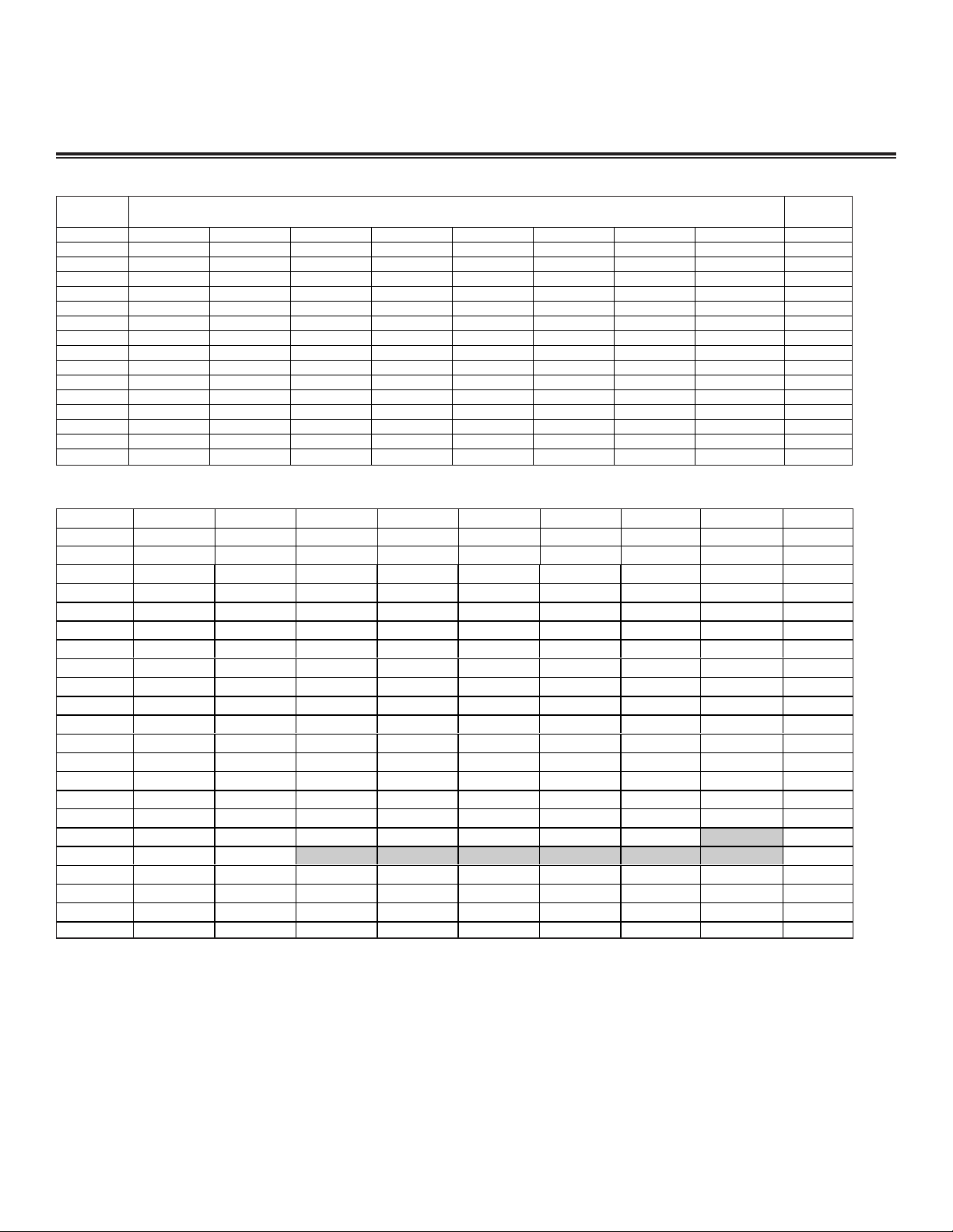
START
ADDRESS
SFR NAMES
END
ADDRESS
80 P4 SP DPL DPH DPL1 DPH1 DPS PCON 87
88 TCON TMOD TL0 TL1 TH0 TH1 CKCON 8F
90 P1 EXIF P4CNT DPX DPX1 C0RMS0 C0RMS1 97
98 SCON0 SBUF0 ESP AP ACON C0TMA0 C0TMA1 9F
A0 P2 P5 P5CNT C0C C0S C0IR C0TE C0RE A7
A8 IE SADDR0 SADDR1 C0M1C C0M2C C0M3C C0M4C C0M5C AF
B0 P3 P6 P6CNT C0M6C C0M7C C0M8C C0M9C C0M10C B7
B8 IP SADEN0 SADEN1 C0M11C C0M12C C0M13C C0M14C C0M15C BF
C0 SCON1 SBUF1 PMR STATUS MCON TA C7
C8 T2CON T2MOD RCAP2L RCAP2H TL2 TH2 COR CF
D0 PSW MCNT0 MCNT1 MA MB MC MCON1 MCON2 D7
D8 WDCON SADDR2 BPA1 BPA2 BPA3 DF
E0 ACC OCAD CSRD CSRA EBS BCUD BCUC E7
E8 EIE MXAX DPX2 DPX3 OWMAD OWMDR EF
F0 B SADEN2 DPL2 DPH2 DPL3 DPH3 DPS1 STATUS1 F7
F8 EIP P7 TL3 TH3 T3CM SCON2 SBUF2 FF
REGISTER
BIT 7 BIT 6 BIT 5 BIT 4 BIT 3 BIT 2 BIT 1 BIT 0
ADDRESS
P4 80h
SP 81h
DPL 82h
DPH 83h
DPL1 84h
DPH1 85h
DPS ID1 ID0 TSL AID SEL1 — — SEL 86h
PCON SMOD_0 SMOD0 OFDF OFDE GF1 GF0 STOP IDLE 87h
TCON TF1 TR1 TF0 TR0 IE1 IT1 IE0 IT0 88h
TMOD GATE C/ T M1 M0 GATE C/T M1 M0 89h
TL0 8Ah
TL1 8Bh
TH0 8Ch
TH1 8Dh
CKCON WD1 WD0 T2M T1M T0M MD2 MD1 MD0 8Eh
P1 90h
EXIF IE5 IE4 IE3 IE2 CKRY RGMD RGSL BGS 91h
P4CNT — — P4CNT.5 P4CNT.4 P4CNT.3 P4CNT.2 P4CNT.1 P4CNT.0 92h
DPX 93h
DPX1 95h
C0RMS0* 96h
C0RMS1* 97h
Maxim Integrated
Special-Function Register Location
High-Speed Microcontroller User’s
Guide: Network Microcontroller
Supplement
18
Page 19

High-Speed Microcontroller User’s
REGISTER
BIT 7 BIT 6 BIT 5 BIT 4 BIT 3 BIT 2 BIT 1 BIT 0
ADDRESS
SCON0 SM0/FE_0 SM1_0 SM2_0 REN_0 TB8_0 RB8_0 TI_0 RI_0 98h
SBUF0 99h
ESP — — — — — — ESP.1 ESP.0 9Bh
AP 9Ch
ACON — — MROM BPME BROM SA AM1 AM0 9Dh
C0TMA0* 9Eh
C0TMA1* 9Fh
P2 A0h
P5 A1h
P5CNT* — CAN0BA — — C0_I/O P5CNT.2 P5CNT.1 P5CNT.0 A2h
C0C* ERIE STIE PDE SIESTA CRST AUTOB ERCS SWINT A3h
C0S* BSS EC96/128 WKS RXS TXS ER2 ER1 ER0 A4h
C0IR* INTIN7 INTIN6 INTIN5 INTIN4 INTIN3 INTIN2 INTIN1 INTIN0 A5h
C0TE* A6h
C0RE* A7h
IE EA ES1 ET2 ES0 ET1 EX1 ET0 EX0 A8h
SADDR0 A9h
SADDR1 AAh
C0M1C* MSRDY ETI ERI INTRQ EXTRQ MTRQ ROW/TIH DTUP ABh
C0M2C* MSRDY ETI ERI INTRQ EXTRQ MTRQ ROW/TIH DTUP ACh
C0M3C* MSRDY ETI ERI INTRQ EXTRQ MTRQ ROW/TIH DTUP ADh
C0M4C* MSRDY ETI ERI INTRQ EXTRQ MTRQ ROW/TIH DTUP AEh
C0M5C* MSRDY ETI ERI INTRQ EXTRQ MTRQ ROW/TIH DTUP AFh
P3 B0h
P6 B1h
P6CNT — — P6CNT.5 P6CNT.4 P6CNT.3 P6CNT.2 P6CNT.1 P6CNT.0 B2h
C0M6C* MSRDY ETI ERI INTRQ EXTRQ MTRQ ROW/TIH DTUP B3h
C0M7C* MSRDY ETI ERI INTRQ EXTRQ MTRQ ROW/TIH DTUP B4h
C0M8C* MSRDY ETI ERI INTRQ EXTRQ MTRQ ROW/TIH DTUP B5h
C0M9C* MSRDY ETI ERI INTRQ EXTRQ MTRQ ROW/TIH DTUP B6h
C0M10C* MSRDY ETI ERI INTRQ EXTRQ MTRQ ROW/TIH DTUP B7h
IP — PS1 PT2 PS0 PT1 PX1 PT0 PX0 B8h
SADEN0 B9h
SADEN1 BAh
C0M11C* MSRDY ETI ERI INTRQ EXTRQ MTRQ ROW/TIH DTUP BBh
C0M12C* MSRDY ETI ERI INTRQ EXTRQ MTRQ ROW/TIH DTUP BCh
C0M13C* MSRDY ETI ERI INTRQ EXTRQ MTRQ ROW/TIH DTUP BDh
C0M14C* MSRDY ETI ERI INTRQ EXTRQ MTRQ ROW/TIH DTUP BEh
C0M15C* MSRDY ETI ERI INTRQ EXTRQ MTRQ ROW/TIH DTUP BFh
SCON1 SM0/FE_1 SM1_1 SM2_1 REN_1 TB8_1 RB8_1 TI_1 RI_1 C0h
SBUF1 C1h
PMR CD1 CD0 SWB CTM 4X/2X ALEOFF — — C4h
STATUS PIP HIP LIP — SPTA1 SPRA1 SPTA0 SPRA0 C5h
MCON* IDM1 IDM0 CMA — PDCE3 PDCE2 PDCE1 PDCE0 C6h
TA C7h
T2CON TF2 EXF2 RCLK TCLK EXEN2 TR2 C/T2 CP/RL2 C8h
T2MOD — — — D13T1 D13T2 — T2OE DCEN C9h
Maxim Integrated
Guide: Network Microcontroller
Supplement
Special-Function Register Location (continued)
19
Page 20

High-Speed Microcontroller User’s
REGISTER
BIT 7 BIT 6 BIT 5 BIT 4 BIT 3 BIT 2 BIT 1 BIT 0
ADDRESS
RCAP2L CAh
RCAP2H CBh
TL2 CCh
TH2 CDh
COR* IRDACK ——C0BPR7 C0BPR6 COD1 COD0 XCLKOE CEh
PSW CY AC F0 RS1 RS0 OV F1 P D0h
MCNT0 LSHIFT CSE SCE MAS4 MAS3 MAS2 MAS1 MAS0 D1h
MCNT1 MST MOF SCB CLM — — — — D2h
MA D3h
MB D4h
MC D5h
MCON1* IRAMD PRAME — — PDCE7 PDCE6 PDCE5 PDCE4 D6h
MCON2* WPIF WPR2 WPR1 WPR0 WPE3 WPE2 WPE1 WPE0 D7h
WDCON SMOD_1 POR EPF1 PF1 WDIF WTRF EWT RWT D8h
SADDR2 D9h
BPA1 DAh
BPA2 DBh
BPA3 DCh
ACC E0h
OCAD E1h
CSRD E3h
CSRA E4h
EBS FPE RBF — BS4 BS3 BS2 BS1 BS0 E5h
BCUD E6h
BCUC BUSY EPMF TIF RIF BC3 BC2 BC1 BC0 E7h
EIE* EPMIE C0IE EAIE EWDI EWPI ES2 ET3 EX2-5 E8h
MXAX EAh
DPX2 EBh
DPX3 EDh
OWMAD — — — — — A2 A1 A0 EEh
OWMDR EFh
B F0h
SADEN2 F1h
DPL2 F2h
DPH2 F3h
DPL3 F4h
DPH3 F5h
DPS1 ID3 ID2 — — — — — — F6h
STATUS1 — — — — V1PF V3PF SPTA2 SPRA2 F7h
EIP* EPMIP C0IP EAIP PWDI PWPI PS2 PT3 PX2-5 F8h
P7 F9h
TL3 FBh
TH3 FCh
T3CM TF3 TR3 T3M SMOD_2 GATE C/T3 M1 M0 FDh
SCON2 SM0/FE_2 SM1_2 SM2_2 REN_2 TB8_2 RB8_2 TI_2 RI_2 FEh
SBUF2 FFh
Maxim Integrated
Guide: Network Microcontroller
Special-Function Register Location (continued)
*Bits in this SFR may have different functions depending on the specific device. Consult the SFR description for details.
Supplement
20
Page 21

High-Speed Microcontroller User’s
REGISTER
BIT 7 BIT 6 BIT 5 BIT 4 BIT 3 BIT 2 BIT 1 BIT 0
ADDRESS
P41111111180h
SP0000011181h
DPL 0 0 0 0 0 0 0 0 82h
DPH 0 0 0 0 0 0 0 0 83h
DPL1 0 0 0 0 0 0 0 0 84h
DPH1 0 0 0 0 0 0 0 0 85h
DPS 0 0 0 0 0 1 0 0 86h
PCON 0 0 SPECIAL 0 0 0 0 0 87h
TCON 0 0 0 0 0 0 0 0 88h
TMOD 0 0 0 0 0 0 0 0 89h
TL0 0 0 0 0 0 0 0 0 8Ah
TL1 0 0 0 0 0 0 0 0 8Bh
TH0 0 0 0 0 0 0 0 0 8Ch
TH1000000008Dh
CKCON 0 0 0 0 0 0 0 1 8Eh
P11111111190h
EXIF 0 0 0 0 SPECIAL SPECIAL SPECIAL 0 91h
P4CNT 1 1 1 1 1 1 1 1 92h
DPX 0 0 0 0 0 0 0 0 93h
DPX1 0 0 0 0 0 0 0 0 95h
C0RMS0* 0 0 0 0 0 0 0 0 96h
C0RMS1* 0 0 0 0 0 0 0 0 97h
SCON0 0 0 0 0 0 0 0 0 98h
SBUF0 0 0 0 0 0 0 0 0 99h
ESP 1 1 1 1 1 1 0 0 9Bh
AP000000009Ch
ACON 1 1 0 0 SPECIAL 0 0 0 9Dh
C0TMA0* 0 0 0 0 0 0 0 0 9Eh
C0TMA1* 0 0 0 0 0 0 0 0 9Fh
P211111111A0h
P511111111A1h
P5CNT* 1 0 0 0 0 0 0 0 A2h
C0C* 0 0 0 0 1 0 0 1 A3h
C0S* 0 0 0 0 0 0 0 0 A4h
C0IR* 0 0 0 0 0 0 0 0 A5h
C0TE* 0 0 0 0 0 0 0 0 A6h
C0RE* 0 0 0 0 0 0 0 0 A7h
IE00000000A8h
SADDR0 0 0 0 0 0 0 0 0 A9h
SADDR1 0 0 0 0 0 0 0 0 AAh
C0M1C* 0 0 0 0 0 0 0 0 ABh
C0M2C* 0 0 0 0 0 0 0 0 ACh
C0M3C* 0 0 0 0 0 0 0 0 ADh
C0M4C* 0 0 0 0 0 0 0 0 AEh
C0M5C* 0 0 0 0 0 0 0 0 AFh
P311111111B0h
P611111111B1h
P6CNT 0 0 0 0 0 0 0 0 B2h
C0M6C* 0 0 0 0 0 0 0 0 B3h
C0M7C* 0 0 0 0 0 0 0 0 B4h
C0M8C* 0 0 0 0 0 0 0 0 B5h
C0M9C* 0 0 0 0 0 0 0 0 B6h
C0M10C* 0 0 0 0 0 0 0 0 B7h
Maxim Integrated
Guide: Network Microcontroller
Supplement
Special-Function Register Reset Values
21
Page 22

High-Speed Microcontroller User’s
REGISTER
BIT 7 BIT 6 BIT 5 BIT 4 BIT 3 BIT 2 BIT 1 BIT 0
ADDRESS
IP10000000B8h
SADEN0 0 0 0 0 0 0 0 0 B9h
SADEN1 0 0 0 0 0 0 0 0 BAh
C0M11C* 0 0 0 0 0 0 0 0 BBh
C0M12C* 0 0 0 0 0 0 0 0 BCh
C0M13C* 0 0 0 0 0 0 0 0 BDh
C0M14C* 0 0 0 0 0 0 0 0 BEh
C0M15C* 0 0 0 0 0 0 0 0 BFh
SCON1 0 0 0 0 0 0 0 0 C0h
SBUF1 0 0 0 0 0 0 0 0 C1h
PMR 1 0 0 0 0 0 1 1 C4h
STATUS 0 0 0 1 0 0 0 0 C5h
MCON* 0 0 0 1 0 0 0 0 C6h
TA11111111C7h
T2CON 0 0 0 0 0 0 0 0 C8h
T2MOD 1 1 0 0 0 1 0 0 C9h
RCAP2L 0 0 0 0 0 0 0 0 CAh
RCAP2H 0 0 0 0 0 0 0 0 CBh
TL200000000CCh
TH2 0 0 0 0 0 0 0 0 CDh
COR* 0 110 0 0 0 0 CEh
PSW 0 0 0 0 0 0 0 0 D0h
MCNT0 0 0 0 0 0 0 0 0 D1h
MCNT1 0 0 0 0 1 1 1 1 D2h
MA00000000D3h
MB00000000D4h
MC00000000D5h
MCON1 SPECIAL SPECIAL 1 1 0 0 0 0 D6h
MCON2 0 0 0 0 0 0 0 0 D7h
WDCON 0 SPECIAL 0 SPECIAL 0 SPECIAL SPECIAL 0 D8h
SADDR2 0 0 0 0 0 0 0 0 D9h
BPA1 0 0 0 0 0 0 0 0 DAh
BPA2 0 0 0 0 0 0 0 0 DBh
BPA3 0 0 0 0 0 0 0 0 DCh
ACC 0 0 0 0 0 0 0 0 E0h
OCAD 0 0 0 0 0 0 0 0 E1h
CSRD 0 0 0 0 0 0 0 0 E3h
CSRA 0 0 0 0 0 0 0 0 E4h
EBS 0 110 0 0 0 0 E5h
BCUD 0 0 0 0 0 0 0 0 E6h
BCUC 0 0 0 0 0 0 0 0 E7h
EIE* 0 0 0 0 0 0 0 0 E8h
MXAX 0 0 0 0 0 0 0 0 EAh
DPX2 0 0 0 0 0 0 0 0 EBh
DPX3 0 0 0 0 0 0 0 0 EDh
OWMAD 0 0 0 0 0 1 1 1 EEh
OWMDR 0 0 0 0 0 0 0 0 EFh
B00000000F0h
Maxim Integrated
Guide: Network Microcontroller
Supplement
Special-Function Register Reset Values (continued)
22
Page 23

High-Speed Microcontroller User’s
REGISTER
BIT 7 BIT 6 BIT 5 BIT 4 BIT 3 BIT 2 BIT 1 BIT 0
ADDRESS
SADEN2 0 0 0 0 0 0 0 0 F1h
DPL2 0 0 0 0 0 0 0 0 F2h
DPH2 0 0 0 0 0 0 0 0 F3h
DPL3 0 0 0 0 0 0 0 0 F4h
DPH3 0 0 0 0 0 0 0 0 F5h
DPS1 0 0 1 1 1 1 1 1 F6h
STATUS1 1 1 1 1 0 0 0 0 F7h
EIP* 0 0 0 0 0 0 0 0 F8h
P711111111F9h
TL3 0 0 0 0 0 0 0 0 FBh
TH3 0 0 0 0 0 0 0 0 FCh
T3CM 0 0 0 0 0 0 0 0 FDh
SCON2 0 0 0 0 0 0 0 0 FEh
SBUF2 0 0 0 0 0 0 0 0 FFh
Maxim Integrated
Guide: Network Microcontroller
Supplement
Special-Function Register Reset Values (continued)
*Bits in this SFR may have different functions depending on the specific device. Consult the SFR description for details.
23
Page 24

High-Speed Microcontroller User’s
7 6543210
SFR 80h
P4.7
A19
P4.6
A18
P4.5
A17
P4.4
A16
P4.3
CE3
P4.2
CE2
P4.1
CE1
P4.0
CE0
RW-0 RW-0 RW-0 RW-0 RW-1 RW-1 RW-1 RW-1
Maxim Integrated
Guide: Network Microcontroller
Supplement
Special-Function Registers
The DS80C400 has many unique features as compared to the standard 8052 microcontroller. These features are controlled by use of
the SFRs located in the unused locations of the 8052 SFR map. While maintaining complete instruction set compatibility with the 8052,
increased functionality is achieved with the DS80C400. The description for each bit indicates its read and write access, as well as its
reset state.
Port 4 (P4)
R = Unrestricted read, W = Unrestricted write, -n = Value after reset
P4.7–0 Port 4 bit 7–0. This port is composed of eight pins that are user-programmable as I/O, extended program
memory chip enables, or extended address lines. The configuration of the eight pins is established
through the programming of the port 4 control register (P4CNT). Following a reset, and if EA is low,
P4.3–P4.1 are driven high and are assigned as chip enables; port pins P4.7–P4.4 and P4.0 are cleared
to a low state and are assigned as addresses and chip enable, respectively. Additional information on
external memory interfacing is found in the port 4 control register SFR description and later sections of
this user’s guide supplement.
A19
Bit 7
A18
Bit 6
A17
Bit 5
A16
Bit 4
CE3
Bit 3
CE2
Bit 2
CE1
Bit 1
CE0
Bit 0
Programmable parallel port. When programmed to function as a general I/O port (thr
ough the
P4CNT.7–P4CNT.0 in the port 4 control register), data written to the P4.7–P4.0 SFR bits results in setting
the port I/O configuration, as well as setting the state on the corresponding port pin. A 1 written to a port
4 latch, previously programmed low (0), activates a high-current, one-shot pullup on the corr
esponding
pin. This is followed by a static, low-current pullup, which remains on until the port is changed again.
The final high state of the port pin is considered a pseudo-input mode and can be easily overdriven from
an external source. Port latches previously in a high-output state do not change, nor does the high-current one-shot fire when a 1 is loaded. Loading a 0 to a port latch results in a static, high-current pulldown on the corresponding pin. This mode is termed the I/O output state, since no weak devices are
used to drive the pin. Port 4 pins, which have previously been assigned to function as an external memory interface (by the PCNT.7–PCNT.0 control bits), are not altered by a write to the port 4 SFR register.
Port 4 alternate function. Port 4 alternate function is established through the programming of the port
4 control register.
Program/data memory address 19. When this bit is set to logic 1 and the P4CNT register is configured
correctly, the corresponding device pin represents the A19 memory signal.
Program/data memory address 18. When this bit is set to logic 1 and the P4CNT register is configured
correctly, the corresponding device pin represents the A18 memory signal.
Program/data memory address 17. When this bit is set to logic 1 and the P4CNT register is configured
correctly, the corresponding device pin repr
esents the A17 memory signal.
Program/data memory address 16. When this bit is set to logic 1 and the P4CNT register is configured
correctly, the corresponding device pin represents the A16 memor
y signal.
Program memory chip enable 3. When this bit is set to logic 1 and the P4CNT register is configured
correctly, the corresponding device pin r
epresents the memory signal.
Program memory chip enable 2. When this bit is set to logic 1 and the P4CNT register is configured
correctly, the corresponding device pin repr
esents the memory signal.
Program memory chip enable 1. When this bit is set to logic 1 and the P4CNT register is configured
correctly, the corresponding device pin r
epresents the memory signal.
Program memory chip enable 0. When this bit is set to logic 1 and the P4CNT register is configured
correctly, the corresponding device pin repr
esents the memory signal.
24
Page 25

High-Speed Microcontroller User’s
7 6543210
SFR 81h SP.7 SP.6 SP.5 SP.4 SP.3 SP.2 SP.1 SP.0
RW-0 RW-0 RW-0 RW-0 RW-0 RW-1 RW-1 RW-1
7 6543210
SFR 82h DPL.7 DPL.6 DPL.5 DPL.4 DPL.3 DPL.2 DPL.1 DPL.0
RW-0 RW-0 RW-0 RW-0 RW-0 RW-0 RW-0 RW-0
76543210
SFR 83h DPH.7 DPH.6 DPH.5 DPH.4 DPH.3 DPH.2 DPH.1 DPH.0
RW-0 RW-0 RW-0 RW-0 RW-0 RW-0 RW-0 RW-0
76543210
SFR 84h DPL1.7 DPL1.6 DPL1.5 DPL1.4 DPL1.3 DPL1.2 DPL1.1 DL1H.0
RW-0 RW-0 RW-0 RW-0 RW-0 RW-0 RW-0 RW-0
76543210
SFR 85h DPH1.7 DPH1.6 DPH1.5 DPH1.4 DPH1.3 DPH1.2 DPH1.1 DPH1.0
RW-0 RW-0 RW-0 RW-0 RW-0 RW-0 RW-0 RW-0
Maxim Integrated
Guide: Network Microcontroller
Supplement
Stack Pointer (SP)
R = Unrestricted read, W = Unrestricted write, -n = Value after reset
SP.7–0
Bits 7–0
Stack pointer. This stack pointer identifies current location of the stack. The stack pointer is incremented before every PUSH operation. This register defaults to 07h after reset. The reset value is used
when the stack is in 8051 stack mode. When the 10-bit stack is enabled (SA = 1), this register is combined with the extended stack pointer (ESP: 9Bh) to form the 10-bit address.
Data Pointer Low 0 (DPL)
R = Unrestricted read, W = Unrestricted write, -n = Value after reset
DPL.7–0
Bits 7–0
Data pointer low 0. This register is the low byte of the standard 8051 data pointer and contains the loworder byte of the 24-bit data address. The data pointer low byte 0 is cleared to 00h on all forms of reset.
Data Pointer High 0 (DPH)
R = Unrestricted read, W = Unrestricted write, -n = Value after reset
DPH.7–0
Bits 7–0
Data pointer high 0. This register is the high byte of the standard 8051 data pointer and contains the
middle-order byte of the 24-bit data address. The data pointer high byte 0 is cleared to 00h on all forms
of reset.
Data Pointer Low 1 (DPL1)
R = Unrestricted read, W = Unrestricted write, -n = Value after reset
DPL1.7–0
Bits 7–0
Data pointer low 1. This register is the low byte of auxiliary data pointer 1 and contains the low-order
byte of the 24-bit data address. When the SEL1: 0 bits (DPS.1:0) are set to 01b, DPX1, DPL1 and DPH1
are used during DPTR operations. The data pointer low byte 1 is cleared to 00h on all forms of reset.
Data Pointer High 1 (DPH1)
R = Unrestricted read, W = Unrestricted write, -n = Value after reset
DPH1.7–0
Bits 7–0
25
Data pointer high 1. This register is the high byte of auxiliary data pointer 1 and contains the middle-
order byte of the 24-bit data address. When the SEL1:0 bits (DPS1:0) are set to 01b, DPX1, DPL1 and
DPH1 are used during DPTR operations. The data pointer high byte 1 is cleared to 00h on all forms of
reset.
Page 26

Data Pointer Select (DPS)
76543210
SFR 86h ID1 ID0 TSL AID SEL1 —
— SEL
RW-0 RW-0 RW-0 R-0 R-0 R-1 RW-0 RW-0
Maxim Integrated
R = Unrestricted read, W = Unrestricted write, -n = Value after reset
High-Speed Microcontroller User’s
Guide: Network Microcontroller
Supplement
ID1, ID0
Bits 7–6
TSL
Bit 5
AID
Bit 4
Reserved
Bits 2, 1
SEL1, SEL
Bits 3, 0
Increment/decrement function select. These bits define whether the INC DTPR instruction 7-6 increments or decrements the active data pointer when DPTR1 or DPTR are selected by the SEL1, SEL bits.
ID1 ID0 SEL1, SEL = 00 SEL1, SEL = 01
0 0 Increment DPTR Increment DPTR1
0
1 0 Increment DPTR Decrement DPTR1
1 1 Decrement DPTR Decr
Toggle select enable. When set, this bit allows the following five DPTR-related instructions to toggle the
SEL bit, followingexecution of the instruction. When TSL = 0, DPTR-related instructions do not affect the
state of the SEL bit. DPTR-related instructions are:
INC DPTRz
MOV DPTR, #data16
MOVC A, @A+DPTR
MOVX @DPTR, A
MOVX A, @DPTR
Automatic increment/decrement enable. This bit allows three of the DPTR-related instructions to increment (or decrement) the content of the active DPTR, if enabled. The actual function (increment or decrement) is dependent on the setting of the ID3, ID2, ID1, and ID0 bits. The active data pointer is incremented (or decremented) by 1 after execution of DPTR-r
When AID is cleared to 0, a DPTR-related instruction does not affect the content of the active DPTR.
This option is affected by the following instructions:
MOVC A, @A+SPTR
MOVX @SPTR, A
MOVX A, @DPTR
Reserved. (Returns 10b when r
other SFR bits in the register when using INC DPS to toggle the pointer selection.
Data pointer select 1, data pointer select. These bits select the active data pointer.
SEL1, SEL = 00: Use DPX, DPH and DPL as DPTR
SEL1, SEL = 01: Use DPX1, DPH1 and DPL1 as DPTR
SEL1, SEL = 10: Use DPX2, DPH2 and DPL2 as DPTR
SEL1, SEL = 11: Use DPX3, DPH3 and DPL3 as DPTR
1 Decrement DPTR Increment DPTR1
ement DPTR1
elated instruction when AID bit is set to logic 1.
ead.) These bits are needed to prevent carr
y passing through the
26
Page 27

High-Speed Microcontroller User’s
76543210
SFR 87h SMOD_0 SMOD0 OFDF ODFE GF1 GF0 STOP IDLE
RW-0 RW-0 RW-0* RW-0 RW-0 RW-0 RW-0 RW-0
Maxim Integrated
Guide: Network Microcontroller
Supplement
Power Control (PCON)
R = Unrestricted read, W = Unrestricted write, -n = Value after reset, * = See description
SMOD_0
Bit 7
SMOD0
Bit 6
OFDF
Bit 5
OFDE
Bit 4
GF1
Bit 3
GF0
Bit 2
STOP
Bit 1
IDLE
Bit 0
Serial port 0 baud-rate doubler enable. This bit enables/disables the serial baud-rate doubling
function for serial port 0.
0 = Serial port 0 baud rate is defined by the baud-rate generation equation.
1 = Serial port 0 baud rate is double that defined by the baud-rate generation equation.
Framing error detection enable. This bit selects the function of the SCON0.7 and SCON1.7, and
SCON2.7.
SMOD0 = 0: SCON0.7, SCON1.7, and SCON2.7 function as SM0 as defined for serial por
SMOD0 = 1: SCON0.7, SCON1.7, and SCON2.7 are converted to the framing error (FE) flag for the
respective serial port.
Oscillator fail-detect flag. When set, this bit indicates that the preceding reset was caused by the
detection of the crystal oscillator frequency falling below approximately 30kHz, if OFDE = 1. OFDF bit
must be clear
when OFDE = 0. OFDF is not set when the processor forces the crystal to stop operation by the stop
mode.
Oscillator fail-detect enable. When the OFDE = 1, a system reset is generated any time the crystal
oscillator frequency falls below approximately 30kHz. This bit does not for
is stopped by the software-enabled stop mode, or if the crystal is stopped when the processor is running from the internal ring oscillator. When the OFDE bit is cleared to logic 0, no reset is issued when
the cr
ystal falls below the 30kHz.
General-purpose user flag 1. This is a bit-addressable, general-purpose flag for software control.
General-purpose user flag 0. This is a bit-addressable, general-purpose flag for software control.
Stop mode select. Setting this bit stops program execution, halts the CPU oscillator and internal timers
and places the CPU in a low-power mode. This bit is cleared and operation is resumed by
an exter
this bit while IDLE = 1 places the device in an undefined state. Setting this bit also clears the CTM
bit. This bit cannot be set while either CAN module is active, i.e., SWINT = CRST = PDE = 0. The following sequence should be used to activate Stop mode: (1) set (CRST or SWINT or PDE) = 1 for
both CANs, (2) clear all CAN bus activity bits for both CANs, (3) set STOP = 1.
Idle mode select. Setting this bit stops program execution, but leaves the CPU oscillator, timers, serial
ports, and interrupts active. This bit is cleared by a reset, or any of the external interrupts, and resumes
mal program execution.
nor
ed by software, and it is not altered by the crystal oscillator frequency falling below 30kHz
ce a reset when the oscillator
nal reset or execution of an enabled external interrupt. This bit is always read as 0. Setting
t control registers.
,
27
Page 28

Timer/Counter Control (TCON)
7 6543210
SFR 88h TF1 TR1 TF0 TR0 IE1 IT1 IE0 IT0
RW-0 RW-0 RW-0 RW-0 RW-0 RW-0 RW-0 RW-0
Maxim Integrated
R = Unrestricted read, W = Unrestricted write, -n = Value after reset
High-Speed Microcontroller User’s
Guide: Network Microcontroller
Supplement
TF1
Bit 7
TR1
Bit 6
TF0
Bit 5
TR0
Bit 4
IE1
Bit 3
IT1
Bit 2
IE0
Bit 1
IT0
Bit 0
Timer 1 overflow flag. This bit indicates when timer 1 overflows its maximum count as defined
by the current mode. This bit can be cleared by software and is automatically cleared when the CPU
vectors to the timer 1 interrupt service routine.
0 = No timer 1 overflow has been detected.
1 = Timer 1 has overflowed its maximum count.
Timer 1 run control. This bit enables/disables the operation of timer 1.
0 = Timer 1 is halted.
1 = Timer 1 is enabled.
Timer 0 overflow flag. This bit indicates when timer 0 overflows its maximum count as defined
by the current mode. This bit can be cleared by software and is automatically cleared when the CPU
vectors to the timer 0 interrupt service r
0 = No timer 0 overflow has been detected.
1 = Timer 0 has overflowed its maximum count.
Timer 0 run control. This bit enables/disables the operation of timer 0.
0 = Timer 0 is halted.
1 = Timer 0 is enabled.
Interrupt 1 edge detect. This bit is set when an edge/level of the type defined by IT1 is
detected. If IT1 = 1, this bit remains set until cleared in software or until the start of the external interrupt
vice routine. If IT1 = 0, this bit inversely reflects the state of the INT1 pin.
1 ser
Interrupt 1 type select. This bit selects whether the INT1 pin detects edge- or level-triggered
interrupts.
0 = INT1 is level triggered.
1 = INT1 is edge triggered.
Interrupt 0 edge detect. This bit is set when an edge/level of the type defined by IT0 is
detected. If IT0 = 1, this bit r
service r
Interrupt 0 type select. This bit selects whether the INT0 pin detects edge- or level-trigger
interrupts.
0
1
outine. If IT0 = 0, this bit inversely r
= INT0 is level trigger
= INT0 is edge triggered.
emains set until clear
ed.
outine or by software.
ed in softwar
eflects the state of the INT0 pin.
e or the star
t of the exter
nal interrupt 0
ed
28
Page 29

High-Speed Microcontroller User’s
7 6543210
SFR 89h GATE C/T M1 M0 GATE C/T M1 M0
RW-0 RW-0 RW-0 RW-0 RW-0 RW-0 RW-0 RW-0
Maxim Integrated
Guide: Network Microcontroller
Supplement
Timer Mode Control (TMOD)
R = Unrestricted read, W = Unrestricted write, -n = Value after reset
GATE
Bit 7
C/T
Bit 6
M1, M0
Bits 5-4
GATE
Bit 3
C/T
Bit 2
M1, M0
Bits 1-0
Timer 1 gate control. This bit enables/disables the ability of timer 1 to increment.
0 = Timer 1 clocks when TR1 = 1, regardless of the state of INT1.
1 = Timer 1 clocks only when TR1 = 1 and INT1 = 1.
Timer 1 counter/timer select.
0 = Timer 1 is incremented by internal clocks.
1 = Timer 1 is incremented by pulses on T1 when TR1 (TCON.6) is 1.
Timer 1 mode select. These bits select the operating mode of timer 1.
M1 M0 Mode
0 0 Mode 0: 8 bits with 5-bit prescale
0 1 Mode 1: 16 bits
1
1 1 Mode 3: Timer 1 is halted but holds its count
Timer 0 gate control. This bit enables/disables the ability of timer 0 to increment.
0 = Timer 0 clocks when TR0 = 1, regardless of the state of INT0.
1 = Timer 0 clocks only when TR0 = 1 and INT0 = 1.
Timer 0 counter/timer select.
0
1 = Timer 0 is incremented by pulses on T0 when TR0 (TCON.4) is 1.
Timer 0 mode select. These bits select the operating mode of timer 0. When timer 0 is in mode 3, TL0
is started/stopped by TR0 and TH0 is started/stopped by TR1. Run control from timer 1 is then provided through the timer 1 mode selection.
M1 M0 Mode
0
0 1
1 0 Mode 2: 8 bits with autoreload
1 1 Mode 3: Two 8-bit timers for timer 0; timer 1 is stopped.
0 Mode 2: 8 bits with autoreload
= Timer incremented by internal clocks.
0 Mode 0: 8 bits with 5-bit prescale
Mode 1: 16 bits
29
Page 30

Timer 0 LSB (TL0)
7 6543210
SFR 8Ah TL0.7 TL0.6 TL0.5 TL0.4 TL0.3 TL0.2 TL0.1 TL0.0
RW-0 RW-0 RW-0 RW-0 RW-0 RW-0 RW-0 RW-0
7 6543210
SFR 8Bh TL1.7 TL1.6 TL1.5 TL1.4 TL1.3 TL1.2 TL1.1 TL1.0
RW-0 RW-0 RW-0 RW-0 RW-0 RW-0 RW-0 RW-0
76543210
SFR 8Ch TH0.7 TH0.6 TH0.5 TH0.4 TH0.3 TH0.2 TH0.1 TH0.0
RW-0 RW-0 RW-0 RW-0 RW-0 RW-0 RW-0 RW-0
76543210
SFR 8Dh TH1.7 TH1.6 TH1.5 TH1.4 TH1.3 TH1.2 TH1.1 TH1.0
RW-0 RW-0 RW-0 RW-0 RW-0 RW-0 RW-0 RW-0
Maxim Integrated
R = Unrestricted read, W = Unrestricted write, -n = Value after reset
High-Speed Microcontroller User’s
Guide: Network Microcontroller
Supplement
TL0.7–0
Timer 0 LSB. This register contains the least significant byte of timer 0.
Bits 7–0
Timer 1 LSB (TL1)
R = Unrestricted read, W = Unrestricted write, -n = Value after reset
TL1.7–0
Timer 1 LSB. This register contains the least significant byte of timer 1.
Bits 7–0
Timer 0 MSB (TH0)
R = Unrestricted read, W = Unrestricted write, -n = Value after reset
TH0.7–0
Timer 0 MSB. This register contains the most significant byte of timer 0.
Bits 7–0
Timer 1 MSB (TH1)
R = Unrestricted read, W = Unrestricted write, -n = Value after reset
TH1.7–0
Timer 1 MSB. This register contains the most significant byte of timer 1.
Bits 7–0
30
Page 31

High-Speed Microcontroller User’s
CLOCK MODE
EXTERNAL CLOCKS PER
SYSTEM CLOCK
Frequency multiplier (4x) 0.25
Frequency multiplier (2x) 0.5
Divide-by-4 1
Power-management mode 256
WD1
WD0
INTERRUPT
TIMEOUT
RESET TIMEOUT
0 0217system clocks
217+ 512 system clocks
01220 system clocks
220 + 512 system clocks
10223 system clocks
223 + 512 system clocks
1 1226 system clocks
226 + 512 system clocks
7 6543210
SFR 8Eh WD1 WD0 T2M T1M T0M MD2 MD1 MD0
RW-0 RW-0 RW-0 RW-0 RW-0 RW-0 RW-0 RW-1
MD2 MD1 MD0
STRETCH
VALUE
MOVX DURATION
0 0 0 0 2 machine cycles
001 1
3 machine cycles
(reset default)
0 1 0 2 4 machine cycles
0 1 1 3 5 machine cycles
1 0 0 4 9 machine cycles
1 0 1 5 10 machine cycles
1 1 0 6 11 machine cycles
1 1 1 7 12 machine cycles
Maxim Integrated
Guide: Network Microcontroller
Supplement
Clock Control (CKCON)
R = Unrestricted read, W = Unrestricted write, -n = Value after reset
WD1, WD0
Bits 7-6
T2M
Bit 5
T1M
Bit 4
T0M
Bit 3
MD2, MD1, MD0
Bits 2-0
Watchdog timer mode select 1-0. These bits are used to select watchdog timeout periods for the
watchdog timer function. The watchdog timer generates interrupt timeout at this periodic rate, when
enabled. All watchdog timer reset timeouts follow the interrupt timeouts by 512 system clock cycles.
The system clock relates to the external clock as follows:
Timer 2 clock select. This bit controls the division of the system clock that drives timer 2. This bit has
no effect when the timer is in baud-rate generator or clock output modes. Clearing this bit to 0 maintains
8051 compatibility. This bit has no effect on instruction cycle timing.
0 = Timer 2 uses a divide-by-12 of the crystal frequency.
1 = Timer 2 uses a divide-by-4 of the system clock frequency.
Timer 1 clock select. This bit controls the division of the system clock that drives timer 1. Clearing this
bit to 0 maintains 8051 compatibility. This bit has no effect on instruction cycle timing.
0 = Timer 1 uses a divide-by-12 of the crystal frequency.
1 = Timer 1 uses a divide-by-4 of the system clock frequency.
Timer 0 clock select. This bit controls the division of the system clock that drives timer 0. Clearing this
bit to 0 maintains 8051 compatibility. This bit has no effect on instruction cycle timing.
= Timer 0 uses a divide-by-12 of the crystal frequency.
0
1 = Timer 0 uses a divide-by-4 of the system clock frequency.
Stretch MOVX select 2-0. These bits select the control timing for external MOVX instructions. All internal
MOVX instructions to the internal MOVX SRAM, as well as CAN 0 data memory registers, occur at t
he fastest
two-machine cycle rate. The internal MOVX rate to the SRAM is not programmable.
31
Page 32

Port 1 (P1)
76543210
SFR 90h
P1.7
INT5
P1.6
INT4
P1.5
INT3
P1.4
INT2
P1.3
TXD1
P1.2
RXD1
P1.1
T2EX
P1.0
T2
RW-1 RW-1 RW-1 RW-1 RW-1 RW-1 RW-1 RW-1
Maxim Integrated
R = Unrestricted read, W = Unrestricted write, -n = Value after reset
High-Speed Microcontroller User’s
Guide: Network Microcontroller
Supplement
P1.7–0
Bits 7–0
INT5
Bit 7
INT4
Bit 6
INT3
Bit 5
INT2
Bit 4
TXD1
Bit 3
RXD1
Bit 2
T2EX
Bit 1
T2
Bit 0
General-purpose I/O port 1. When serving as a general-purpose I/O port, all the pins have an alternative function as described later. P1.2–7 contains functions that are new to the 80C32 architecture. The
timer 2 functions on pins P1.1-0 are available on the 80C32, but not on the 80C31. Each of the functions
is controlled by several other SFRs. The associated port 1 latch bit must contain a logic 1 before the pin
can be used in its alternate function capacity.
External interrupt 5. A falling edge on this pin causes an external interrupt 5, if enabled.
External interrupt 4. A rising edge on this pin causes an external interrupt 4, if enabled.
External interrupt 3. A falling edge on this pin causes an external interrupt 3, if enabled.
External interrupt 2. A rising edge on this pin causes an external interrupt 2, if enabled.
Serial port 1 transmit. This pin transmits the serial por
t 1 data in serial port modes 1, 2, and 3, and
emits the synchronizing clock in serial port mode 0.
Serial port 1 receive. This pin receives the serial port 1 data in serial port modes 1, 2, and 3, and is a
bidirectional data transfer pin in serial port mode 0.
Timer 2 capture/reload trigger. A 1-to-0 transition on this pin causes the value in the T2 registers to be
transfer
to-0 transition on this pin r
red into the capture registers, if enabled by EXEN2 (T2CON.3). When in autoreload mode, a 1-
eloads the timer 2 registers with the value in RCAP2L and RCAP2H, if enabled
by EXEN2 (T2CON.3).
Timer 2 external input. A 1-to-0 transition on this pin causes timer 2 increment or decr
ement, depend-
ing on the timer configuration.
32
Page 33

High-Speed Microcontroller User’s
7 6543210
SFR 91h IE5 IE4 IE3 IE2 CKRY RGMD RGSL BGS
RW-0 RW-0 RW-0 RW-0 R-* R-* RW-* RT-0
Maxim Integrated
Guide: Network Microcontroller
Supplement
External Interrupt Flag (EXIF)
R = Unrestricted read, W = Unrestricted write, T = Timed-access write only, -n = Value after reset, * = Bits 1, 2 and 3 are cleared to 000b by a power-on reset, but are
unchanged by all other forms of reset.
IE5
Bit 7
IE4
Bit 6
IE3
Bit 5
IE2
Bit 4
CKRY
Bit 3
RGMD
Bit 2
RGSL
Bit 1
BGS
Bit 0
External interrupt 5 flag. This bit is set when a falling edge is detected on INT5. This bit must be
cleared manually by software. Setting this bit in software causes an interrupt if enabled. Please note that,
when the EOWMI bit internal to the 1-Wire bus master is set to 1, the IE5 flag serves as the 1-Wire bus
master interrupt flag.
External interrupt 4 flag. This bit is set when a rising edge is detected on INT4. This bit must be cleared
manually by software. Setting this bit in software causes an interrupt, if enabled.
External interrupt 3 flag. This bit is set when a falling edge is detected on INT3. This bit must be
clear
ed manually by software. Setting this bit in software causes an interrupt, if enabled.
External interrupt 2 flag. This bit is set when a rising edge is detected on INT2. This bit must be cleared
manually by software. Setting this bit in software causes an interrupt, if enabled.
Clock ready. The CKRY bit indicates the status of the startup period delay used by the cr
tor and the crystal clock multiplier warmup period. CKR
ing. When the CKRY = 1, the counter has completed. This bit is cleared each time the CTM bit in the
PMR r
egister is changed from low to high to start the crystal multiplier
out is removed on the CD1, CD0 bits to select the multiplied crystal clock as a system clock source. This
status bit is also cleared each time the crystal oscillator is restarted when exiting stop mode.
Ring mode status. This bit indicates the current clock source for the device. This bit is cleared to 0 after
a power-on reset, and is unchanged by all other forms of reset.
0 = Device is operating from the external crystal or oscillator.
1 = Device is operating from the ring oscillator.
Ring oscillator select. This bit selects the clock source following a resume from stop mode. Using the
ring oscillator to r
after a power-on reset and is unchanged by all other forms of reset. The state of this bit is undefined on
devices that do not incorporate a ring oscillator.
0 = The device holds operation until the crystal oscillator has warmed up.
1 = The device begins operating fr
switches to the external clock source or oscillator.
Bandgap select. This bit enables/disables the bandgap reference during stop mode. Disabling the
bandgap reference provides significant power savings in stop mode, but sacrifices the ability to perfor
a power-fail interrupt or power-fail reset while stopped. This bit can only be modified with a timed access
procedure.
0 = The bandgap reference is disabled in stop mode, but functions during normal operation.
1 = The bandgap refer
esume fr
om stop mode allows almost instantaneous startup. This bit is cleared to 0
om the ring oscillator and, when the crystal warmup is complete, it
ence operates in stop mode.
Y = 0 indicates the startup delay is still count-
. Once the CKRY is set, the lock-
ystal oscilla-
m
33
Page 34

Port 4 Control Register (P4CNT)
76543210
SFR 92h - - P4CNT.5 P4CNT.4 P4CNT.3 P4CNT.2 P4CNT.1 P4CNT.0
RT-1 RT-1 RT-1 RT-1 RT-1 RT-1 RT-1 RT-1
PORT PIN FUNCTION
P4CNT.5-3
P6.5
P6.4
P4.7
P4.6
P4.5
P4.4
MAX
MEMORY
SIZE PER
CEx
000
I/O
I/O
I/O
I/O
I/O
I/O
32kB
001
I/O
I/O
I/O
I/O
I/O
A16
128kB
010
I/O
I/O
I/O
I/O
A17
A16
256kB
011
I/O
I/O
I/O
A18
A17
A16
512kB
100
I/O
I/O
A19
A18
A17
A16
1MB
101
I/O
A20
A19
A18
A17
A16
2MB
110 or 111
A21
A20
A19
A18
A17
A16
4MB
Maxim Integrated
R = Unrestricted read, T = Timed-access write only, -n = Value after reset
High-Speed Microcontroller User’s
Guide: Network Microcontroller
Supplement
P4CNT.5–0
Bit 7
Bit 6
P4CNT.5-P4CNT.3
Port 4 control register. P4CNT bits provide the configuration for the alternate addressing modes on port
4 and 6. These settings, in turn, establish the size of the external program memory that can be accessed.
To prevent an unauthorized change in the external memory configuration, all writes to the P4CNT must
use the timed-access function. Programming the bit combinations given in this section converts the designated port pins to I/O, address, or chip enables. Once any bit combination containing a 1 is programmed into P4CNT.2-P4CNT.0, the corresponding port pins that are then assigned to chip enables are
locked out from being programmed as I/O in the port 4 SFR. In a similar fashion, any bit combination
containing a 1 programmed into P4CNT.5-P4CNT.3 locks out the corresponding port pins (P6.5-P6.4,
P4.7–P4.4) assigned to addresses. This allows the normal use of the port SFR, without the concern that
a byte write to the SFR alters any of the external chip enables or addresses. Following a reset, the P4CNT
is set to FFh, which, in turn, assigns all of the port 4 and P6.5-4 pins to address bits and chip enables.
This register should be programmed to reflect the actual system memory configuration.
Reserved.
Reserved.
Port pin P6.5, P6.4, P4.7–4 configuration control bits for CEx. Bits 5-0 configure the external mem-
ory control signals. P4CNT.5-3 determine whether specific P6 and P4 pins function as A21–A16 or I/O.
The number of external address lines enabled establishes the range for each program chip enable
(CE0-3) and data chip enable (PCE0-3). When P4CNT.5-3 = 000b, CE0–CE3 are decoded on 32kB
block boundaries.
CE0–CE7 can be individually configured as program or program/data memory by the MCON and
MCON1 SFRs. When CE0–CE7 are conver
ted from program to program/data memory, PCE0–PCE3 are
disabled if the corresponding data memory area is covered by CEx. The internally decoded range for
each program chip enable (CE0–CE7) is established by the number of external address lines (A21–A16)
enabled by the P4CNT.5–P4CNT.3 control bits. The following table outlines the assigned memory boundaries of each chip enable (CEx
) as determined by the P4CNT.5-P4CNT.3 control bits. (The memory
boundaries of each peripheral chip enable (PCEx) are determined by P6CNT.5-P6CNT.3.) Note that,
when the external address bus is limited to A0–A15, the chip enables are internally decoded on a 32kB
x 8 block boundary. This is to allow the use of the more common 32kB memories, as opposed to using
a less common 64kB block size memory.
34
Page 35
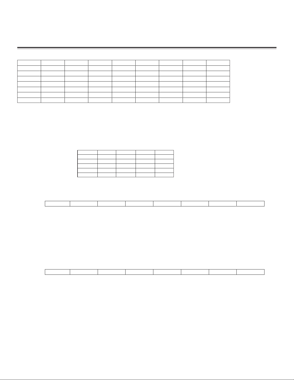
High-Speed Microcontroller User’s
P4CNT.5-3
CE0 CE1 CE2 CE3 CE4 CE5 CE6 CE7
000 32K 32-64K 64-96K 96-128K 128-160K 160-192K 192-224K 224-256K
001 128K 128-256K 256-384K 384-512K 512-640K 640-768K 768-896K
896-1024K
010 256K 256-512K 512-768K
768-1024K
1024-1280K
1280-1536K
1536-1792K
1792-2048K
011 512K .512-1M 1-1.5M 1.5-2M 2-2.5M 2.5-3M 3-3.5M 3.5-4M
100 1M 1-2M 2-3M 3-4M 4-5M 5-6M 6-7M 7-8M
101 2M 2-4M 4-6M 6-8M 8-10M 10-12M 12-14M 14-16M
110 or 111
4M 4-8M 8-12M 12-16M — — — —
P4CNT.2-0
P4.3 P4.2 P4.1 P4.0
000 I/O I/O I/O I/O
100 I/O I/O I/O CE0
101 I/O I/O CE1 CE0
110 I/O CE2 CE1 CE0
111 CE3 CE2 CE1 CE0
76543210
SFR 93h DPX.7 DPX.6 DPX.5 DPX.4 DPX.3 DPX.2 DPX.1 DPX.0
RW-0 RW-0 RW-0 RW-0 RW-0 RW-0 RW-0 RW-0
76543210
SFR 95h DPX1.7 DPX1.6 DPX1.5 DPX1.4 DPX1.3 DPX1.2 DPX1.1 DPX1.0
RW-0 RW-0 RW-0 RW-0 RW-0 RW-0 RW-0 RW-0
Maxim Integrated
Guide: Network Microcontroller
Supplement
Program Memory Chip-Enable Boundaries
P4CNT.2-P4CNT.0 Port pin P4.3–P4.0 configuration control bits. P4CNT.2-0 determines whether specific P4 pins
function as program chip-enable signals or I/O. The memory ranges for each CEx signal are determined
by P4CNT.5-3. Note that, when the appropriate PDCEx bit (MCON.3–0) is set, the corresponding CEx
pin functions as a combined program/peripheral chip enable, and the respective PCE0–PCE3 is disabled. CE4–CE7 are enabled via P6CNT.2–0.
CE0–CE3 Chip-Enable Function Selection
Data Pointer Extended Register 0 (DPX)
R = Unrestricted read, W = Unrestricted write, -n = Value after reset
DPX.7–0
Bits 7–0
Data pointer extended register 0. This register contains the high-order byte of the extended 24-bit
address for data pointer 0. This register is used only in the 24-bit paged and contiguous addressing
modes. This register is not used for addressing the data memory in the 16-bit addressing mode and,
therefore, can be utilized as a scratchpad SRAM register.
Data Pointer Extended Register 1 (DPX1)
R = Unrestricted read, W = Unrestricted write, -n = Value after reset
DPX1.7–0
Bits 7–0
Data pointer extended register 1. This register contains the high-order byte of the extended 24-bit
address for auxiliary data pointer 1. This register is used only in the 24-bit paged and contiguous
addressing modes. This register is not used for addressing the data memory in the 16-bit addressing
mode and, therefore, can be utilized as a scratchpad SRAM register.
35
Page 36

High-Speed Microcontroller User’s
7 6543210
SFR 96h C0RMS0.7 C0RMS0.6 C0RMS0.5 C0RMS0.4 C0RMS0.3 C0RMS0.2 C0RMS0.1 C0RMS0.0
R-0 R-0 R-0 R-0 R-0 R-0 R-0 R-0
Maxim Integrated
Guide: Network Microcontroller
CAN 0 Receive Message Stored Register 0 (C0RMS0)
R = Unrestricted read, -n = Value after reset. The C0RMS0 is cleared to 00h on all forms of reset, including the reset established by the CRST bit.
This SFR is not present on the DS80C411.
Supplement
C0RMS0.7–0
C0RMS0.7
Bit 7
C0RMS0.6
Bit 6
C0RMS0.5
Bit 5
C0RMS0.4
Bit 4
C0RMS0.3
Bit 3
C0RMS0.2
Bit 2
C0RMS0.1
Bit 1
C0RMS0.0
Bit 0
CAN 0 receive message stored register 0. The C0RMS0 bits indicate which message center (1–8) has
successfully received and stored the last incoming message. The content of the C0RMS0 register is
updated each time a new message is successfully received and stored. The contents of the C0RMS0
register are automatically cleared following each read of C0RMS0 by the microcontroller. A bit value 1
indicates that the assigned message center has successfully received and stored new data since the
last read of the C0RMS0 register. A bit value 0 indicates that no new message has been successfully
received and stored since the last read of the RMS0 register. No interrupts are asserted because of the
C0RMS0 settings. This register works fully independent of the status bits in the CAN status register and
the INTIN7–0 vector in the CAN interrupt register, as well as of the INTRQ bit in the CAN message control registers.
Message center 8, message received and stored.
Message center 7, message received and stored.
Message center 6, message received and stored.
Message center 5, message received and stored.
Message center 4, message received and stored.
Message center 3, message received and stored.
Message center 2, message received and stored.
Message center 1, message received and stored.
36
Page 37

High-Speed Microcontroller User’s
76543210
SFR 97h CORMS1.7 CORMS1.6 CORMS1.5 CORMS1.4 CORMS1.3 CORMS1.2 CORMS1.1 CORMS1.0
R-0 R-0 R-0 R-0 R-0 R-0 R-0 R-0
Maxim Integrated
Guide: Network Microcontroller
Supplement
CAN 0 Receive Message Stored Register 1 (C0RMS1)
R = Unrestricted read, -n = Value after reset. The C0RMS0 is cleared to 00h on all forms of reset, including the reset established by the CRST bit.
This SFR is not present on the DS80C411.
C0RMS1.7–0
Bits 7–0
C0RMS1.7
Bit 7
C0RMS1.6
Bit 6
C0RMS1.5
Bit 5
C0RMS1.4
Bit 4
C0RMS1.3
Bit 3
C0RMS1.2
Bit 2
C0RMS1.1
Bit 1
C0RMS1.0
Bit 0
CAN 0 receive message stored register 1. The C0RMS1 bits indicate which message center (9–15)
has successfully received and stored the last incoming message. The content of the C0RMS1 register
is updated each time a new message is successfully received and stored. The contents of the C0RMS1
register are automatically cleared following each read of C0RMS1 by the microcontroller. A bit value 1
indicates that the assigned message center has successfully received and stored new data since the
last read of the C0RMS1 register. A bit value 0 indicates that no new message has been successfully
received and stored since the last read of the RMS1 register. No interrupts are asserted because of the
C0RMS1 settings. This register works fully independent of the status bits in the CAN status register and
the INTIN7–0 vector in the CAN interrupt register, as well as of the INTRQ bit in the CAN message control registers.
Reserved.
Message center 15, message received and stored.
Message center 14, message received and stored.
Message center 13, message received and stored.
Message center 12, message received and stored.
Message center 1
Message center 10, message received and stored.
Message center 9, message received and stored.
1, message received and stored.
37
Page 38

Serial Port 0 Control (SCON0)
7 6543210
SFR 98h SM0/FE_0 SM1_0 SM2_0 REN_0 TB8_0 RB8_0 TI_0 RI_0
RW-0 RW-0 RW-0 RW-0 RW-0 RW-0 RW-0 RW-0
MODE
SM2
SM1
SM0
FUNCTION
LENGTH
PERIOD
0000Synchronous 8 bits 12 t
CLK
0100Synchronous 8 bits 4 t
CLK
1x10Asynchronous 10 bits Timer 1 or 2
2001Asynchronous 11 bits 64 t
CLK
(SMOD_0 = 0)
2001Asynchronous 11 bits 32 t
CLK
(SMOD_0 = 1)
210
1
Asynchronous (MP)
11 bits 64 t
CLK
(SMOD_0 = 0)
210
1
Asynchronous (MP)
11 bits 34 t
CLK
(SMOD_0 = 1)
3011Asynchronous 11 bits Timer 1 or 2
311
1
Asynchronous (MP)
11 bits Timer 1 or 2
76543210
SFR 99h SBUF0.7 SBUF0.6 SBUF0.5 SBUF0.4 SBUF0.3 SBUF0.2 SBUF0.1 SBUF0.0
RW-0 RW-0 RW-0 RW-0 RW-0 RW-0 RW-0 RW-0
Maxim Integrated
R = Unrestricted read, W = Unrestricted write, -n = Value after reset
High-Speed Microcontroller User’s
Guide: Network Microcontroller
Supplement
SM0/FE_0
Bit 7
SM1_0
Bit 6
SM2_0
Bit 5
REN_0
Bit 4
TB8_0
Bit 3
RB8_0
Bit 2
TI_0
Bit 1
RI_0
Bit 0
Serial port 0 mode bit 0. (When SMOD0 is logic 0.) When SMOD0 is logic 1, it is the framing error flag
that is set upon detection of an invalid stop bit and must be cleared by software. When SMOD0 is set,
modification of this bit has no effect on the serial mode setting.
Serial port 0 mode bit 1.
Serial port 0 mode bit 2. Setting of this bit in mode 1 ignores reception if an invalid stop bit is
detected. Setting this bit in mode 2 or 3 enables multipr
ocessor communications. This prevents the RI_0
bit from being set, and interrupt being asserted, if the 9th bit received is 0.
Receiver enable. This bit enable/disables the serial port 0 receiver shift register.
0 = Serial port 0 reception disabled.
1 = Serial port 0 r
eceiver enabled (modes 1, 2, and 3). Initiate synchronous reception (mode 0).
9th transmission bit state. This bit defines the state of the 9th transmission bit in serial port 0 modes
2 and 3.
9th received bit state. This bit identifies that state of the 9th reception bit of received data in ser
ial port 0 modes 2 and 3. When SM2_0 = 0, RB8_0 is the state of the stop bit in mode 1. RB8_0 is not
used in mode 0.
Transmitter interrupt flag. This bit indicates that data in the serial port 0 buffer has been completely
shifted out. In serial por
t mode 0, TI_0 is set at the end of the 8th data bit. In all other modes, this bit is
set at the end of the last data bit. This bit must be cleared by software.
Receiver interrupt flag. This bit indicates that a byte of data has been received in the serial port 0
buffer. In serial port mode 0, RI_0 is set at the end of the 8th bit. In serial port mode 1, RI_0 is set after
the last sample of the incoming stop bit subject to the state of SM2_0. In modes 2 and 3, RI_0 is set after
the last sample of RB8_0. This bit must be cleared by softwar
e.
-
Serial Data Buffer 0 (SBUF0)
R = Unrestricted read, W = Unrestricted write, -n = Value after reset
SBUF0.7–0
Bits 7–0
Serial data buffer 0. Data for serial port 0 is read from or written to this location. The serial transmit and
receive buffers are separate registers, but both are addressed at this location.
38
Page 39

High-Speed Microcontroller User’s
7
6
5 43210
SFR 9Bh — — — — — — ESP.1 ESP.0
RW-1 RW-1 RW-1 RW-1 RW-1 RW-1 RW-0 RW-0
7
6
543210
SFR 9Ch AP.7 AP.6 AP.5 AP.4 AP.3 AP.2 AP.1 AP.0
RW-0 RW-0 RW-0 RW-0 RW-0 RW-0 RW-0 RW-0
Maxim Integrated
Guide: Network Microcontroller
Supplement
Extended Stack Pointer Register (ESP)
R = Unrestricted read, W = Unrestricted write, -n = Value after reset
Bits 7–2
ESP.1-0
Bits 1-0
Reserved.
Extended stack pointer. These extended stack pointer bits are used with SP to form a 10-bit stack
pointer to support the use of the 1kB of the internal data memory as stack memory. When SA = 1, any
overflow of the SP from FFh to 00h increments the ESP by 1, and any under flow of the SP from 00h to
FFh decrements the ESP by 1. The ESP register is not used as part of the stack pointer when the default
stack memory location is selected (SA = 0), but is still r
MOVX SRAM through the IDM1: 0 bits does not alter the ability of the ESP and SP registers to properly
access the internal memory. See MCON register for more detail.
Address Page Register (AP)
R = Unrestricted read, W = Unrestricted write, -n = Value after reset
AP.7–0
Bits 7–0
Address page register. The address page register (AP) is a paging register, which is used with the 24bit paged addressing mode to support extended 24-bit program and data addressing capabilities, and
is fully compatible with the original 8052 16-bit addressing operation. The AP register and the higherorder byte of the program counter (PC23: 16) are cleared to 00 hex, following a system reset, to establish initial program execution in the first 64kB page (page 0). When the microcontroller is programmed to
operate in the 24-bit paged addressing mode (AM1, AM0 = 01b), data programmed into the AP register
is loaded into the program counter high-order byte when the processor executes an LJMP or LCALL
instruction. Execution of any of these two instructions loads the AP into the high-order byte of the program
counter (PC23: 16) to allow the program counter (PC) to drive address lines A23–A16 with the previous
AP value at the same time as the lower 16 bits (A0–A15) of the PC are updated.
In this manner, software compiled using the standard 16-bit addressing scheme uses the contents of
the AP to establish the page to which the program flow is to jump. The AP register can be loaded at any
time prior to the execution of the above two instructions to establish the address vector, which is used
when the LJMP or LCALL instruction is used to cross page boundaries. Note that the third byte of the
program counter (PC23: 16) does not increment when the lower 16 bits in the lower two bytes of the PC
roll over from FFFF hex to 0000 hex. PC23: 16 functions only as a holding register to issue high-order
address (A23–A16) when the 24-paged addressing mode is enabled. All interrupts are handled by
pushing the high byte of the program counter (PC23: 16) along with the standard push of the standard
16-bit program counter on to the stack before the hardware generated interrupt LCALL instruction is
executed. The AP register is not altered during the interrupt and must be taken into consideration when
doing another LJMP or LCALL instruction within the interrupt routine.
Typically, it is best to do a PUSH AP when entering the interrupt routine, and a POP AP when exiting, if either
LJMP or LCALL instructions are to be used inside the routine with a new page address assigned to the AP.
The additional loading of PC23: 16 on to the stack results in one additional machine cycle during an interrupt
and three bytes being stored on the stack. Following the execution of a RETI instruction, the processor automatically reloads the entire 24 value of the PC with the original address from the stack. Again, the RETI or
RET requires one additional machine cycle when compared to the standard 16-bit address-only operation.
The address page register is not used with the PC when the AM0 and AM1 bits are programmed for
either the 16-bit addressing or 24-bit contiguous addressing mode, but it is accessible as a general-purpose SFR register.
ead/write accessible. Relocating the internal
39
Page 40

High-Speed Microcontroller User’s
7 6543210
SFR 9Dh — — MROM BPME BROM SA AM1 AM0
RT-1 RT-1 RT-0 RT-0 RT-X RT-0 RT-0 RT-0
MROM
LOWER 32kB ROM MEMORY LOCATION (HEX)
0 000000–007FFF (reset default)
1 FF0000–FF7FFF
AM1
AM0
ADDRESSING MODE
0
0
16-bit addressing mode
(A23–A16 are locked to 00h)
0
1
24-bit paged addressing mode
1
x
24-bit contiguous addressing mode
Maxim Integrated
Guide: Network Microcontroller
Supplement
Address Control Register (ACON)
R = Unrestricted read, T = Timed access write only, -n = Value after reset. The address control register is cleared to 1100 x 000b on all forms of reset, but bit 3 is reset to
0 on power-on reset.
Bits 7-6
MROM
Bit 5
BPME
Bit 4
BROM
Bit 3
SA
Bit 2
AM1, AM0
Bits 1-0
Reserved.
Merge ROM assignment. The MROM bit provides a software mechanism for mapping the lower 32kB
internal ROM block to one of the two following address locations. The upper 32kB internal ROM block
is always mapped to FF8000h–FFFFFFh of the program memory space.
Breakpoint mode enable. Setting this bit to 1 enables the software breakpoint mode. Once enabled,
the processor can enter or exit the breakpoint mode by executing an A5h instruction. Clearing this bit
to 0 disables the A5h instruction to the processor, and no breakpoint mode operation is allowed.
Bypass ROM. This bit determines whether the program flow is to start in the external user program or
the internal ROM after a reset. A 0 forces the processor to start execution at location 000000h of internal ROM after a reset if the EA pin is connected high. A 1 forces the processor to start user program
execution at location 000000h of the program memory after a r
eset if the EA pin is connected high.
Connecting the EA pin to ground always forces the processor to start user program execution at location 000000h of the program memory after a reset, r
egardless of the logic state of the BROM bit. This bit
is reset to 0 upon power-on. Changing this bit from a 0 to a 1 when the EA pin is connected high causes a reset immediately
. Changing this bit from a 1 to a 0 has no immediate effect on the system function
until a reset occurs.
Extended stack address mode enable. Programming the SA bit to a 0 enables the standard 256
scratchpad SRAM bytes as the default stack. In this mode, the standard 8-bit stack pointer value is supplied by the SP register. ESP is not used in this mode. Programming the SA bit to a 1 enables the alternate use of 1kB of the internal data memory as the stack memory. In this mode, the 2 least significant
bits of the ESP register are used as the two most significant bits of the 10-bit stack pointer.
Address mode control bits.
The AM0 and AM1 bits establish the addressing mode for the microcontr
oller.
Programming AM1 and AM0 to a 00 leaves the microcontroller in the traditional 8051 16-bit addressing
mode. In this mode, the processor operates with a 16-bit address field with the higher-order program
counter byte (PC23:16) forced to 00h.
Programming AM1 and AM0 to a 01 enables the 24-bit paged addr
essing mode. In this mode, the
processor operates with a 24-bit address field with the address page register (AP) functioning as the
input source to load the high-order program counter byte (PC23:16) during the execution of specific
instructions.
40
Page 41

High-Speed Microcontroller User’s
7 6543210
SFR 9Eh C0TMA0.7 C0TMA0.6 C0TMA0.5 C0TMA0.4 C0TMA0.3 C0TMA0.2 C0TMA0.1 C0TMA0.0
R-0 R-0 R-0 R-0 R-0 R-0 R-0 R-0
Maxim Integrated
Guide: Network Microcontroller
Supplement
Programming AM1 and AM0 to 10 or 11 enables the fully contiguous 24-bit program counter-addressing mode. In this mode, the processor addresses program memory with a full 24-bit program counter
(A23–A0) and does not utilize the AP register as an input to the program counter. AP is converted into
a general-purpose read/write SFR and does not have any relationship to the program counter or address
field. Note that AM1 and AM0 bits default to 00 on all resets, so the 24-bit contiguous address mode
must be enabled before executing the following four instructions:
1) MOV DPTR, #data24
2) ACALL addr19
3) LCALL addr24
4) LJMP addr24
CAN 0 Transmit Message Acknowledgment Register 0 (C0TMA0)
R = Unrestricted read, -n = Value after reset. The C0TMA0 is cleared to 00h on all forms of reset, including the reset established by the CRST bit.
This SFR is not present on the DS80C411.
C0TMA0.7–0
Bits 7-0
C0TMA0.7
Bit 7
C0TMA0.6
Bit 6
C0TMA0.5
Bit 5
C0TMA0.4
Bit 4
C0TMA0.3
Bit 3
C0TMA0.2
Bit 2
C0TMA0.1
Bit 1
C0TMA0.0
Bit 0
CAN 0 transmit message acknowledgment register 0. The C0TMA0 bits indicate which message center (1–8) has successfully transmitted a message since the last read of the register. The contents of the
C0TMA0 register are updated each time a new message is successfully transmitted. The contents of the
C0TMA0 register are automatically cleared following each read of C0TMA0 by the microcontroller. A bit
value of 1 indicates that the assigned message center has been successfully transmitted since the last
read of the C0TMA0 register. A bit value of 0 indicates that no new message has been successfully
transmitted since the last read of the C0TMA0 register. Interrupts are not generated as a result of bits
being set in the C0TM0 register. This register works fully independent of the status bits in the CAN status register, the INTIN7–0 vector in the CAN interrupt register, and the INTRQ bit in the CAN message
control registers.
Message center 8, message transmitted.
Message center 7, message transmitted.
Message center 6, message transmitted.
Message center 5, message transmitted.
Message center 4, message transmitted.
Message center 3, message transmitted.
Message center 2, message transmitted.
Message center 1, message transmitted.
41
Page 42

High-Speed Microcontroller User’s
7 6543210
SFR 9Fh — C0TMA1.6 C0TMA1.5 C0TMA1.4 C0TMA1.3 C0TMA1.2 C0TMA1.1 C0TMA1.0
R-0 R-0 R-0 R-0 R-0 R-0 R-0 R-0
Maxim Integrated
Guide: Network Microcontroller
CAN 0 Transmit Message Acknowledgment Register 1 (C0TMA1)
R = Unrestricted read, -n = Value after reset. The C0TMA0 is cleared to 00h on all forms of reset, including the reset established by the CRST bit.
This SFR is not present on the DS80C411.
Supplement
C0TMA1.6–0
Bits 7-0
Bit 7
C0TMA1.6
Bit 6
C0TMA1.5
Bit 5
C0TMA1.4
Bit 4
C0TMA1.3
Bit 3
C0TMA1.2
Bit 2
C0TMA1.1
Bit 1
C0TMA1.0
Bit 0
CAN 0 transmit message acknowledgment register 1. The C0TMA1 bits indicate which message center (1–8) has been successfully transmitted. The contents of the C0TMA1 register are updated each time
a new message is successfully transmitted. The contents of the C0TMA1 register are automatically
cleared following each read of C0TMA1 by the microcontroller. A bit value of 1 indicates that the
assigned message center has been successfully transmitted since the last read of the C0TMA1 register. A bit value of 0 indicates that no new message has been successfully transmitted since the last read
of the C0TMA1 register. The corresponding C0TMA1 bits are assigned to the following message centers. No interrupts are asserted because of the C0TMA1 settings. This register works fully independent
of the status bits in the CAN status register and the INTIN7–0 vector in the CAN interrupt register, as well
as of the INTRQ bit in the CAN message control registers (same as C0TMA0).
Reserved.
Message center 15, message transmitted.
Message center 14, message transmitted.
Message center 13, message transmitted.
Message center 12, message transmitted.
Message center 11, message transmitted.
Message center 10, message transmitted.
Message center 9, message transmitted.
42
Page 43

High-Speed Microcontroller User’s
7 6543210
SFR A0h A15/P2.7 A14/P2.6 A13/P2.5 A12/P2.4 A11/P2.3 A10/P2.2 A9/P2.1 A8/P2.0
RW-1 RW-1 RW-1 RW-1 RW-1 RW-1 RW-1 RW-1
76543210
SFR A1h
P5.7
PCE3
P5.6
PCE2
P5.5
PCE1
P5.4
PCE0
P5.3
—
P5.2
T3
P5.1
C0RX
P5.0
C0TX
RW-1 RW-1 RW-1 RW-1 RW-1 RW-1 RW-1 RW-1
Maxim Integrated
Guide: Network Microcontroller
Supplement
Port 2 (P2)
R = Unrestricted read, W = Unrestricted write, -n = Value after reset
P2.7–0
Bits 7–0
Port 2. This port functions as an address bus during external memory access and as a general-purpose
I/O port on devices that incorporate internal program memory. During external memory cycles, this port
contains the MSB of the address. The only instructions to access the P2 SFR are MOVX A, @Ri and
MOVX @Ri, A when port 2 is used as the MSB of an external address.
Port 5 (P5)
R = Unrestricted read, W = Unrestricted write, -n = Value after reset
P5.7–0
Bits 7–0
PCE3
Bit 7
PCE2
Bit 6
PCE1
Bit 5
PCE0
Bit 4
Bit 3
T3
Bit 2
C0RX
Bit 1
C0TX
Bit 0
Port 5. This port can function as a programmable parallel I/O port, a CAN interface, timer 3 input, and/or
peripheral enable signals. Data written to the port latch serves to set both logic level and direction of the
data on the pin. A 1 written to a port latch, previously programmed low (0), activates a high-current, oneshot pullup on the corresponding pin. This is followed by a static, low-current pullup that remains on until
the port is changed again. The final high state of the port pin is considered a pseudo-input mode and
can be easily overdriven from an external source. Port latches previously in a high-output state do not
change, nor does the high-current one-shot fire when a 1 is loaded. Loading a 0 to a port latch results
in a static, high-current pulldown on the corresponding pin. This mode is termed the I/O output state,
since no weak devices are used to drive the pin.
Writes to P5.1–P5.0 are disabled when the P5CNT.3 bit in the port 5 control SFR is programmed to a 1.
These bits read as a 1 when assigned to the CAN processor. The P5.2 latch bit must be set to 1 before
the pin can be used for the alternate function of T3. The value of the port latch is not altered by a read
operation, except the read-modify-write instructions that perform a read followed by a write. See P5CNT
SFR (A2h) for more details.
Peripheral chip enable 3. When enabled by the P5CNT r
signal.
Peripheral chip enable 2. When enabled by the P5CNT register, this pin asserts the third chip-enable
signal.
Peripheral chip enable 1. When enabled by the P5CNT register, this pin asserts the second chipenable signal.
Peripheral chip enable 0. When enabled by the P5CNT register, this pin asserts the first chip-enable
signal.
Reserved.
Timer/counter 3 external input. This pin functions as an external input to timer 3 when configur
such with the T3CM SFR. A 1-to-0 transition on this pin incr
CAN 0 receive. This pin is connected to the receive data-output pin of the CAN 0 transceiver device.
CAN 0 transmit. This pin is connected to the transmit data-input pin of the CAN 0 transceiver device.
egister, this pin asserts the fourth chip-enable
ed as
ements timer 3.
43
Page 44

High-Speed Microcontroller User’s
76543210
SFR A2h — CAN0BA — — C0_I/O P5CNT.2 P5CNT.1 P5CNT.0
RW-1 RW-0 RW-0 RW-0 RW-0 RT-0 RT-0 RT-0
P5CNT.2-0
P5.7 P5.6 P5.5 P5.4
000 I/O I/O I/O I/O
100 I/O I/O I/O PCE0
101 I/O I/O PCE1 PCE0
110 I/O PCE2 PCE1 PCE0
111 PCE3 PCE2 PCE1 PCE0
Maxim Integrated
Port 5 Control Register (P5CNT)
R = Unrestricted read, W = Unrestricted write, T = Timed Access Write Only, -n = Value after reset
Guide: Network Microcontroller
Supplement
Bit 7
CAN0BA
Bit 6
Bit 5
Bit 4
C0_I/O
Bit 3
P5CNT.2-P5CNT.0
Bits 2-0
Reserved. Read returns logic 1.
CAN 0 bus active status. The CAN0BA signal is a latched status bit that is set if the respective CAN 0
I/O-enabled (P5CNT.3) bit is set and bus activity is detected on the CAN 0 bus. Once activity is detected and the bit is set, it remains set until cleared by application software or a reset. This bit is not used
on the DS80C411 and returns an indeterminate value.
Reserved. Read returns logic 0.
Reserved. Read returns logic 0.
CAN 0 I/O enable. The P5CNT.3 bit configur
es P5.0 and P5.1 as either standar
d I/O or CAN receive input
(P5.1–C0RX) and CAN transmit output (P5.0–C0TX). Programming P5CNT.3 to a 0 places P5.1 and P5.0 into
the standard I/O mode. Programming P5CNT.3 to a 1 places P5.1 and P5.0 into the CAN transmit and receive
mode. When P5CNT.3 is programmed to a 1, all I/O interaction through the port 5 SFR with P5.1 and P5.0 is
disabled. This bit must be set to 1 on the DS80C411.
Port pin P5.7–P5.4 configuration control bits. Once any bit combination containing a 1 is pr
ogrammed into P5CNT.2-P5CNT.0, the corresponding port pins that are then assigned to peripheral chip
enable are locked out from being programmed as I/O in the port 5 SFR. The internally decoded range
for each peripheral chip enable (PCE0–PCE3) is established by the number of external addr
ess lines
(A19–A16), which are enabled by the P6CNT.5-P6CNT.3 control bits. This can be different than the program memory CE0–CE7 decoding. The following table outlines the assigned data memory boundaries
of each chip enable as determined by the P6CNT.5-P6CNT.3 control bits. Note that, when the external
address bus is limited to A0–A15, the chip enables are internally decoded on a 32kB x 8 block boundar
y. This is to allow the use of the more common memories, as opposed to using a less common 64kB
block size memory.
PCEx CHIP-ENABLE SELECTION FUNCTION
PCE0–PCE3 are internally decoded to data memory address block boundaries as determined by the
P6CNT.5–P6CNT.3 control bits. When any of CE0–CE7 are converted from a program chip enable to program/data chip enables through the MCON and MCON1 registers, data memory areas assigned to
PCE0–PCE3 are automatically disabled when the corresponding memory area is covered by CE0–CE7.
Enabling merged program/data memory access under CE0–CE7 does not alter the port 5 control register bit states. Returning the CE0–CE7 enables back to the program memory automatically reenables
the respective PCE0–PCE3 relationship.
44
Page 45

High-Speed Microcontroller User’s
7 6543210
SFR A3h ERIE STIE PDE SIESTA CRST AUTOB ERCS SWINT
RW-0 RW-0 RW-0 RW-0 RT-1 RW-0 RW-0 RT-1
Maxim Integrated
Guide: Network Microcontroller
Supplement
CAN 0 Control Register (C0C)
R = Unrestricted read, W = Unrestricted write, T = Timed-access write only, -n = Value after reset
This SFR is not present on the DS80C411.
ERIE
Bit 7
STIE
Bit 6
PDE
Bit 5
SIESTA
Bit 4
CAN 0 error interrupt enable. Programming the ERIE bit to a 1 enables the CAN 0 status bus status
(BSS) or error count greater than 96 bit (EC96) to issue an interrupt to the microcontroller, if the C0IE bit
in the EIE SFR is also set. When ERIE is cleared to a 0, the error interrupt is disabled.
CAN 0 status interrupt enable. Programming the STIE bit to a 1 allows the CAN 0 status error bits (ER0ER2), the transmit status bit (TXS), the receive status bit (RXS), or the wake-up status bit (WKS) to issue
an interrupt to the microcontroller, if the C0IE bit in the EIE SFR is also set. When STIE is cleared to a 0,
the status interrupt is disabled.
CAN 0 power-down enable. Programming the PDE bit to a 1 places the CAN 0 controller into a fully
tic power-down mode after completion of the last reception, transmission, or after the arbitr
or an error condition occurred. Note that the term ‘after arbitration lost’ denotes the fact the arbitration was
lost and the reception following this lost arbitration is completed. Recall that the CAN processor immediately becomes a receiver after it has lost its arbitration on the CAN bus. Programming PDE = 0 disables
the power-down mode. The PDE mode forces all of the CAN 0 logic to a static state. The PDE mode can
only be removed by either software reprogramming the PDE bit or through a system reset. A read of PDE
establishes when the power-down mode has been enabled or removed as per the PDE bit. In all cases,
the CAN controller begins operation after 11 recessive bits (a power-up sequence) on the CAN bus per
the configuration settings for bit timing, which were programmed prior to entering the power-down mode.
Since WKS reflects when the CAN has entered the low-power state, as per the SIESTA and/or PDE bit
states, a read of the PDE bit establishes when the PDE bit is actually allowed to enable the low-power
state. If the low-power state was previously enabled by setting the SIESTA bit, a read of PDE reflects the
actual PDE bit value and not the low-power mode. If the low-power mode has not been previously
enabled and the PDE bit is set to a 1 by software, a read of PDE returns a 0, until such time the PDE bit
actually enables the low-power mode following an active transmit or receive operation. When the PDE and
SIESTA bit are not used together, a read of the PDE bit, by default, also reflects the actual state of the lowpower mode. Setting PDE does not alter any CAN block controls or error status relationships.
Low-power mode. Setting the SIESTA bit to a 1 places the CAN 0 controller into a low-power static state
after completion of the last reception, transmission, or after the arbitration was lost or an error condition
occurred. Note that the term ‘after arbitration lost’ denotes the fact the arbitration was lost and the reception following this lost arbitration is completed. Recall that the CAN processor immediately becomes a
receiver after it has lost its arbitration on the CAN bus. Programming SIESTA = 0 disables the low-power
mode. The state of when the SIESTA mode is actually enabled or removed, as per the SIESTA bit pr
grammed value, is reflected in the read of the SIESTA bit. The SIESTA mode is removed when the CAN
0 controller detects CAN 0 bus activity, by reprogramming the SIESTA bit to a 0, or by setting either
CRST or SWINT to a 1. When the SIESTA bit is cleared by either a microcontroller write or activity on the
CAN 0 bus, the CAN controller begins operation after 11 recessive bits on the CAN bus (after a powerup sequence) using the configuration settings that were programmed prior to entering the power-down
mode. Changing the SIESTA bit from a 0 to a 1 does not disrupt a currently active receive or transmit,
but allows the completion of CAN 0 bus activity prior to entering into the static state. If the CAN 0 logic
issues an interrupt as a result of an active CAN 0 receive or transmit while SIESTA is being set, the SIESTA bit is cleared, and the CAN 0 logic does not enter the low-power mode. Since WKS reflects when the
CAN has entered the low-power state, as per the SIESTA and/or PDM bit states, a read of the SIESTA
bit establishes when the SIESTA bit is actually allowed to enable the low-power state. If the low-power
state was previously enabled by setting the PDM bit, a read of SIESTA reflects the actual SIESTA bit
value, and not the low-power mode. If the low-power mode has not been previously enabled and the
SIESTA bit is set to a 1 by software, a read of SIESTA returns a 0 until such time that the SIESTA bit actually enables the low-power mode, following an active transmit or receive operation. When the PDE and
SIESTA bit are not used together, a read of the SIESTA bit, by default, also reflects the actual state of the
ation was lost
sta-
o-
45
Page 46

CRST
Maxim Integrated
Bit 3
AUTOB
Bit 2
High-Speed Microcontroller User’s
Guide: Network Microcontroller
Supplement
low-power mode. Setting SIESTA does not alter any CAN block controls or error status relationships.
Note that the PDE and SIESTA bits act independent of each other. Setting both bits leaves the CAN
processor in a low-power state until both bits have been cleared by their respective mechanisms.
CAN 0 reset. (Requires a timed-access write.) When CRST is set to a 1 and after completion of the last
reception, transmission, or after arbitration was lost or an error condition occurred, all CAN registers
located in the SFR memory map, with the exception of the CAN 0 control register are cleared to a 00
hex. The CAN 0 control register is set to 09 hex. Note that the term ‘after arbitration lost’ denotes the fact
the arbitration was lost and the reception following this lost arbitration is completed. Recall that the CAN
ocessor immediately becomes a receiver after it has lost its arbitration on the CAN bus. In accordance
pr
with waiting until after the completion of the last reception, transmission, or after arbitration was lost or
an error condition occurred, a read of the CRST bit, when previously programmed to a 1, returns a 0,
until such time that the CRST = 1 state is actually allowed to place the CAN processor into the reset
state. As such, a read of the CRST bit verifies when the CAN reset has been engaged or removed. CAN
registers located in the MOVX memory map are left in the last state prior to setting CRST. Setting CRST
also clears both the receive- and transmit-error counters in the CAN controllers and sets the SWINT bit
to a 1. CRST must be cleared by software to remove the CAN reset and allow the CAN 0 processor to
be initialized. When the CAN processor is not in a bus-off mode (BSS = 0) and the CAN processor exits
either the software initialization mode (SWINT programmed from a 1 to a 0) or when the CAN reset is
removed (CRST bit is cleared from a 1 to a 0 and the SWINT bit is cleared from 1 to 0), the CAN processor performs a power-up sequence of 11 consecutive recessive bits before the CAN controller enters
into normal operation. If the CAN reset is removed and SWINT is left in the software initialization state,
the microcontroller is allowed to immediately start programming the CAN registers and MOVX data
memory prior to the completion of the power-up sequence. Exiting the software initialization mode
(SWINT ≥ 0) requires a power-up sequence of 11 consecutive recessive bits before the CAN controller
enters into normal operation. Clearing CRST to a 0 from a previous 0 state does not alter CAN processor operation. All writes to the CRST bit require a timed-access function.
Autobaud. When AUTOB is set to a 1, an internal loopback is enabled to AND the data from the external CAN bus with the transmitted data of the CAN 0 processor. The “ANDed’ data is then connected to
the internal input of the CAN 0 processor. At the same time, the transmitted data is disabled from reaching the external C0TX pin. The C0TX pin is placed into a recessive state when AUTOB = 1. The purpose of the internal loopback and the disabled C0TX pin is to allow the CAN processor to establish the
proper CAN bus timing without disrupting the normal data flow between other nodes on the CAN bus.
Disabling the C0TX pin and setting the C0TX pin to a r
driving nonsynchronized data onto the CAN bus (creating CAN bus errors to other nodes) when being
programmed with various frequencies to synchronize the processor with the CAN bus. With AUTOB =
1, the microcontroller autobaud algorithm makes use of the CAN 0 status register RXS and error status
bits to determine when a message is successfully received (when AUTOB = 1, a successful receive, a
store is not required). Each successive baud-rate attempt is proceeded by the microcontroller clearing
the transmit- and receive-error counters by a write of 00 to the transmit-error SFR register and a read of
the CAN 0 status register to clear the previous status-change interrupt. Note that a write to the transmiterror SFR register automatically resets the CAN fault confinement state machine to an initial (error-active)
state if the error counters are cleared to 00 hex. If, however, the error counters are programmed to a
value greater than 128, the CAN processor is in an error-passive state. Appropriate flags are set when
the error counter is written with any value. A write of the status register is also used to remove the previous error value in the ER2–ER0 bits. Clearing the error counters also clears the EC96 bit, if set. When
BSS = 1, the CAN processor locks out the ability for the microcontroller to write to the error counters by
virtue of the fact that the SWINT bit is also forced to a 0 state during the period that the CAN processor
performs a bus recovery and power-up sequence. Once the CAN processor has removed itself from the
bus-off condition, it also clears BSS = 0, sets SWINT = 1, and clears both the transmit- and receive-error
counters to 00 hex. Imagine a system with only two nodes on the CAN bus.
The following two situations are examples of how the autobaud function works on the CAN processor. In
the first case, consider three nodes, A, B, and C, with nodes A and B operating in the normal CAN operational mode (nonautobaud) and node C (a DS80C400 CAN processor) attempting to establish a proper baud rate using the autobaud features. If node A transmits a message, node B acknowledges this
message, and node C also receives the acknowledged message if it has the same baud rate. If node C
does not have the same baud rate as nodes A and B, node C detects the mismatch by the respective
error count. Node C then proceeds to adapt its baud rate and attempt to receive the following message.
ecessive state prevents the CAN processor from
46
Page 47

High-Speed Microcontroller User’s
Maxim Integrated
Guide: Network Microcontroller
Supplement
In the second case, consider a system with only two nodes on the CAN bus. Consider node A in the
autobaud mode and the second node on the bus in the normal CAN operational mode. Node B transmits a message and does not receive an acknowledgment, since there is no third node on the bus that
is also properly synchronized with the bus and in the normal CAN operational mode. Once node B
enters into an error-passive mode (after 16 repeated messages), it begins to send passive error flags.
Note that, when node B is operating in an error-passive mode, it does not send any dominant errors flags
to the bus. Once node A has established the proper baud rate, it receives the correct message. The
internal autobaud loopback path also allows the passive acknowledgment error sent by node B to be
“ANDed” with the dominant, internally transmitted acknowledgment bit from node A. As such, node A
sees no errors, which establishes the fact that it is properly synchronized with the bus. Node A now exits
out of the autobaud mode (AUTOB = 0) and enters into the normal CAN operational mode (with full
transmit capability to the CAN bus). In this mode, node A then acknowledges the next message from
node B.
ERCS
Bit 1
SWINT
Bit 0
Error count select. The ERCS bit establishes in which level the error counters set or clear the X96/128
bit in the CAN 0 status register. When ERCS = 0, the EC96/128 flag operates in an EC96 mode. In this
mode, the EC96/128 bit is set to a 1 whenever the error count of either the transmit- or receive-error
counters exceed 96. When ERCS = 1, the EC96/128 flag operates in an EC128 mode. In the EC128
mode, the EC96/128 flag is set to a 1 whenever the error count of either the transmit- or receive-error
counters reach a level of 128 or greater.
Software initialization. (Unrestricted r
establishes the initialization state for CAN 0, which disables CAN 0 bus activity to allow the processor
to modify the MOVX SRAM assigned to the message centers without corrupting messages. When
SWINT is set to 1 and after completion of the last reception or transmission, after arbitration was lost, or
after an error condition occurred, all CAN 0 bus activity is disabled, allowing the processor to initialize
any or all of the CAN 0 MOVX SRAM. Note that the term ‘after arbitration lost’ denotes the fact the arbitration was lost and the reception following this lost arbitration is completed. Recall that the CAN processor immediately becomes a receiver after it has lost its arbitration on the CAN bus. A read of the SWINT
bit verifies when the CAN processor software initialization mode has been engaged or removed.
Although the transmit- and r
transmit- and receive-error counters can be altered by software through the use of the CAN 0 transmiterror SFR register, as long as SWINT = 1. Setting SWINT to a 1 also clears the SIESTA bit independent
of what is stored to the SIESTA bit location during or prior to the write of the C0C register. Clearing SWINT
= 0 hardware also disables the microcontroller from writing to the first 16 bytes of the CAN MOVX memory. These 16 locations make up the CAN 0 control/status/mask registers. When SWINT = 0, the microcontroller is allowed to write to any of the MOVX CAN register sites. All MOVX registers are readable at
any time, independent of the SWINT bit. Also note that the SWINT bit does not alter the read or write
access to any of the CAN 0 SFR registers or MOVX CAN message center registers. SWINT is programmed to a 0 when the processor has completed the MOVX SRAM initialization and CAN 0 bus activity has started. Software write access to the error counters is disabled when SWINT is cleared to a 0. A
bus-off condition is caused by a high number of errors on the CAN bus. When a bus-off condition
occurs, the CAN processor clears the SWINT bit to a 0 and immediately starts a bus recover and powerup sequence. During this time, the microcontroller is limited to only reading this bit. All microcontroller
write access to SWINT is disabled when BSS = 1.
If the SWINT bit is set by a system reset, programming the CRST bit or setting the SWINT bit without the
prior detection of a bus-off condition can cause an adverse condition. Clearing SWINT by software
allows the CAN processor to synchronize itself to the CAN bus after the CAN processor executes a
power-up sequence (11 recessive bits). The power-up sequence requires the CAN processor to detect
11 consecutive recessive bits. (In CAN protocol, this is termed a power-up sequence.) When SWINT =
0 by a bus-off condition, bus off forces the CAN processor to initiate a standard bus-off recovery
sequence (128kB x 11 recessive bits). This is followed by entering into a reset state, requiring a powerup sequence (11 recessive bits), after which the CAN processor enters into the idle state (normal operation, BSS = 0) and sets the SWINT bit to a 1. This bit is not intended for use in changing data within
the message centers after the CAN processor is placed into operation. Changes to the arbitration or
data fields in the message centers should be done through the use of the MSRDY bit in the respective
message (1–15) control registers. The SWINT bit is locked into the SWINT = 1 state until the bus timing
registers are programmed to valid states. (The invalid states are 00 hex. See the CAN bus timing registers in the CAN control/status/mask registers.)
ead/write if BSS = 0, and read only if BSS = 1.) The SWINT bit
eceive-error counters are not cleared when the SWINT bit is set, the CAN 0
47
Page 48

CAN 0 Status Register (C0S)
7 6543210
SFR A4h BSS EC96/128 WKS RXS TXS ER2 ER1 ER0
R-0 R-0 R-0 RW-0 RW-0 RW-0 R-0 R-0
Maxim Integrated
R = Unrestricted read, W = Unrestricted write, -n = Value after reset
This SFR is not present on the DS80C411.
High-Speed Microcontroller User’s
Guide: Network Microcontroller
Supplement
C0S.7–0
Bits 7-0
BSS
Bit 7
EC96/128
Bit 6
CAN 0 status register. The first three bits, BSS, EC96, and WKS, and the last 3 bits, ER2–ER0, in the
CAN status register are read only by the microcontroller. The CAN processor sets or clears these flags
(and interrupt sources) as defined by the system aspects associated with each bit. A CAN status register read clears the internal status-change interrupt flag. Unlike RXS and TXS, however, the individual
mechanisms that set the ER2, ER0, BSS, EC96, and WKS bits do not reoccur without first being removed
by the CAN processor. As a result, a new (0 ≥ 1) change by BSS, EC96, or (1 ≥ 0) change by WKS is
required to set a new internal status change interrupt flag through these bits. In a similar fashion, a read
of the CAN status register (which automatically sets ER2–ER0 to 111), followed by a new transmit or
receive error, is required to set a new internal status change interrupt flag. If any one of these bits
changes state from a previous 0 to a 1 (other than WKS, which changes from a 1 to a 0) and STIE is set
to 1 with no other interrupt pending, the INTIN vector in the CAN interrupt register is set to 01 hex. If TXS
or RXS is set to a 1 and a second message is successfully transmitted or received, and STIE is set to 1
while no other interrupt is pending, the INTIN vector in the CAN interrupt register is also set to 01 hex.
If ER[2:0] changes from either a 000 or 111 binary state to any state other than 000 or 111, the INTIN
vector in the CAN interrupt register is also set to 01 hex. This issues a status change interrupt request
if at least one of the following conditions is valid and no other interrupt is pending.
CAN 0 bus status. (Read only.) The BSS bit reflects the current status of the CAN 0 bus. When BSS =
1, the CAN 0 bus is disabled (bus off) and is not capable of receiving or transmitting messages. This
condition is the result of the transmit-error counter reaching a count of 256. When the CAN processor
detects an error count of 256, the CAN processor automatically sets BSS = 1 and clears SWINT = 0.
BSS is cleared to a 0 to enable CAN 0 bus activity when the CAN processor completes both the bus-off
recovery (128kB x 11 consecutive r
sive bits). Once the CAN processor has completed this relationship, it sets SWINT = 1 and enters into
the software initialization state. Once the microcontroller has cleared SWINT to a 0, the CAN processor
is enabled to transmit and receive messages. BSS is set to a 1 whenever the transmit error counter for
CAN 0 reaches the 256 limit. When BSS = 0, the CAN 0 bus is enabled to receive or transmit messages.
A change in the state of BSS from a previous 0 to a 1 generates an interrupt if the ERIE, C0IE, and IE
SFR register bits are set. All microcontroller writes to the SWINT bit are disabled when BSS = 1. Both the
transmit- and receive-error counters are cleared to 00 hex when the bus-off condition is cleared by the
CAN module and BSS is cleared to 0.
CAN 0 error count greater than 96/128 status. (Read only.) The EC96/128 bit operates in one of two
modes. These two modes are determined by the state of the C0C.1 bit in the CAN 0 control register.
Following a system or CAN reset, the C0C.1 bit is cleared to a 0, which in turn enables the EC96 mode.
C0C.1 = 0, EC96/128 = EC96. In this mode, when EC96/128 = 1, the interrupt flag indicates that either
the CAN 0 transmit error counter or the CAN 0 receive error counter has exceeded an error count of 96,
an exceptional high number of er
receive error counter both have an error count of less than 97. A change in the state of EC96/128 from
a previous 0 to a 1 generates an interr
is programmed to a 1, the EC96/128 bit is reconfigured into an EC128 bit flag mode.
C0C.1 = 1, EC96/128 = EC128. In this mode, when EC96/128 = 1, the interrupt flag indicates that either
the CAN 0 transmit error counter or the CAN 0 receive error counter has reached an error count of 128,
an exceptional number of errors. EC96/128 = 0 indicates that the current transmit error counter and
receive error counter both have an error count of less than 128. A change in the state of EC96/128 from
either a previous 0 to a 1 or from a previous 1 to a 0 generates an interrupt if the ERIE, C0IE and IE SFR
register bits are set.
ecessive bits) and the power-up sequence (11 consecutive reces-
rors. EC96/128 = 0 indicates that the current transmit error counter and
upt if the ERIE, C0IE, and IE SFR register bits are set. When C0C.1
48
Page 49

High-Speed Microcontroller User’s
Maxim Integrated
Guide: Network Microcontroller
Supplement
WKS
Bit 5
RXS
Bit 4
TXS
Bit 3
CAN 0 wake-up status. (Read only.) WKS = 0 indicates that the CAN 0 is not in a low-power mode. WKS
= 1 indicates that CAN 0 is in a low-power mode, based on the setting of either the SIESTA bit or the
power-down mode bit to a 1. Clearing both the SIESTA bit and power-down enable (PDE) bit forces the
WKS bit to a 0. A change in the state of WKS from a previous 1 to a 0 generates an interrupt if the STIE,
C0IE, and IE SFR register bits are set.
Receive status. The RXS bit functions in two modes. When the AUTOB bit is set to a 1, RXS = 1 indicates that a message has been successfully received by CAN 0 since the last read of the CAN 0 status
register. Note that this does not mean that the incoming message was or was not stored in a message
center, but means that the message did not have any errors associated with it during the reception.
Messages that are successfully received but are not stored do not pass the arbitration filtering tests
required by the internal message centers. When the AUTOB bit is cleared to a 0, RXS = 1 indicates that
a message has been both successfully received and stored in one of the message centers by CAN 0
since the last read of the CAN 0 status register.
RXS = 0 indicates that no message has been successfully received since the last read of the CAN 0 status register. RXS is set only by the CAN 0 logic and is not cleared by the CAN controller. It is cleared
only by the microcontroller software, the CRST bit, or a system reset.
When the RXS bit (0 > 1) provides the interrupt source for an interrupt, the microcontroller is required to
read the CAN status register to clear the internal status-change interrupt flag. This flag is seen externally
by the presence of the 01 state in the CAN interrupt register. Once this flag is cleared, the 01 state in
the CAN interrupt register is replaced with either the 00 state for no interrupts pending or a lower-priority interrupt code related to one of the message centers. If a second successful reception is detected
prior to or after the clearing of the RXS bit in the status register, a second status-change interrupt flag is
set to allow a second interrupt to be issued. Each new successful reception generates an interrupt
request independent of the previous state of the RXS bit, as long as the CAN status register has been
read to clear the previous status-change interrupt flag. Note that if the microcontroller sets the RXS bit
from a previous low, it generates an artificial status-change interrupt (STIE = 1).
Thus, if RXS is previously set to 0 and a reception was successful, RXS is set to 1 and an interrupt can
be asserted if enabled. If the microcontroller writes a 1 to RXS when RXS was previously a 0, RXS is set
to a 1 and an interrupt can be asserted if enabled. If RXS is previously set to 1 and a reception was successful, RXS stays set to a 1 and an interrupt can be asserted if enabled. If the microcontroller writes a
1 to RXS when RXS was previously a 1, RXS remains 1 and no interrupt is asserted.
Transmit status. TXS = 1 indicates that a message has been successfully transmitted by CAN 0 (error
free and acknowledged) since the last read of the CAN 0 status register. TXS = 0 indicates that no message has been successfully transmitted since the last read of the CAN 0 status register. TXS is set only
by the CAN 0 logic and is not cleared by the CAN controller but is cleared only by the microcontroller
software, the CRST bit, or a system reset.
When the TXS bit (0 > 1) pr
read the CAN status register to clear the internal status-change interrupt flag (this flag is seen externally by the presence of the 01 state in the CAN interrupt register). Once this flag is cleared, the 01 state
in the CAN interrupt register is replaced with either the 00 state for no interrupts pending or a lower-priority interrupt code related to one of the message centers. If a second successful transmission is detected prior to or after the clearing of the TXS bit in the status register, a second status-change interrupt flag
is set to allow a second interrupt to be issued. Each new successful transmission generates an interrupt
request independent of the previous state of the TXS bit, as long as the CAN status register has been
read to clear the previous status-change interrupt flag. Note that, if the microcontroller sets the TXS bit
from a previous low, it generates an artificial status-change interrupt (STIE = 1).
Thus, if TXS is previously set to 0 and a transmission was successful, TXS is set to 1 and an interrupt
can be asserted if enabled. If the microcontroller writes a 1 to TXS when TXS was previously a 0, TXS is
set to a 1 and an interrupt can be asserted if enabled. If TXS is previously set to 1 and a transmission
was successful, TXS stays set to a 1 and an interrupt can be asserted if enabled. If the microcontroller
writes a 1 to TXS when TXS was previously a 1, TXS remains 1 and no interrupt is asserted.
ovides the interrupt source for an interrupt, the microcontroller is required to
49
Page 50

High-Speed Microcontroller User’s
ER2
ER1
ER0
PRIORITY
ERROR CONDITIONS
0 0 0 N/A No error in last frame
0 0 1 2 Bit stuff error
0 1 0 5 Format error
011 4
Transmit not
acknowledged error
100
6 (lowest)
Bit 1 error
101
1 (highest)
Bit 0 error
1 1 0 3 CRC error
1 1 1 N/A
No change since last C0S
read
Maxim Integrated
Guide: Network Microcontroller
Supplement
ER2-0
Bits 2-0
CAN 0 bus error status 2-0. The ER2–ER0 bits indicate the first type of error that is encountered within a CAN 0 bus frame. The following states outline the specific error type. The eighth state (111 binary)
is automatically programmed into ER2–ER0, following a read of the CAN 0 status register to establish if
there has been a change in an error condition when doing a future read of the CAN 0 status register.
The status data (ER2–ER0) read by the processor must be analyzed or stored in a separate SRAM location, since the ER2–ER0 bits are automatically set to the 111 state following a read. The 111 state
remains in the register until a new frame is either transmitted or received, at which time the ER2–ER0
data is undated in relation to the associated transmit or receive message. The ER2–ER0 bits are read
only. Any attempted write to these bits does not affect the bits or the interrupt relationship associated
with their value.
The interrupt error represented by the ER2–ER0 bus error bits is updated following each reception or
transmission. Since the stored error from one reception or transmission can be reproduced in the next
attempted reception or transmission, a new interrupt is generated whenever a new error condition is
detected. This occurs during a reception or transmission, as long as the previous error condition was
removed by a read of the CAN 0 status register.
Thus, if ER2-ER0 is set to 000 or 111 and an error condition occurs, this error condition is stored in the
ER2-ER0 bits. An interrupt request is made to the microcontroller whenever the ER2-ER0 values change
from either a 000 or 111 binary state to any state other than 000 or 111. If a second error occurs prior
to the microcontroller performing a read of the CAN status register, then the second error is not stored
and the first error condition continues to reside in the ER2-ER0 bits. Once the CAN status register is read
by the microcontroller, the error status bits are set to 111. If another error occurs after the microcontroller
read of the CAN status register, the ER2-ER0 bits are updated with the new error condition.
If two errors come up at the same time, only the one with the higher priority (as in the following table) is
shown. Priority 1 is the highest and 6 is the lowest priority. The format error is higher than the bit 1 error,
since the format error is always a bit 1 error, but a bit 1 error is not necessarily a format error. The error
value displayed is selected according to relevance, if the two errors occur at the same time. This is based
on which error is the main error and which one is an accompanying error.
The following is a description of error types:
Bit stuff error: The CAN controller detects more than five consecutive bits of an identical state in an
incoming message.
Format error: A received message has the wrong format.
Transmit not acknowledged error: A data frame was sent and the requested node did not acknowl-
edge the message.
Bit 1 error: The CAN attempted to transmit a message and that, when a recessive bit was transmitted,
the CAN bus was found to have a dominant bit level. This error is not generated when the bit is a part
of the arbitration field (identifier and remote retransmission request).
Bit 0 error: The CAN attempted to transmit a message and that, when a dominant bit was transmitted,
the CAN bus was found to have a recessive bit level. This error is not generated when the bit is a part
of the arbitration field. The bit 0 error is set each time a r
the CAN processor is recovering fr
om a bus-off recovery period.
ecessive bit is received during the period that
CRC error: The calculated CRC of a received message does not match the CRC embedded in the message.
50
Page 51

High-Speed Microcontroller User’s
76543210
SFR A5h INTIN7 INTIN6 INTIN5 INTIN4 INTIN3 INTIN2 INTIN1 INTIN0
R-0 R-0 R-0 R-0 R-0 R-0 R-0 R-0
Maxim Integrated
Guide: Network Microcontroller
Supplement
CAN 0 Interrupt Register (C0IR)
R = Unrestricted read, W = Unrestricted write, -n = Value after reset
This SFR is not present on the DS80C411.
INTIN7–0
Bits 7–0
CAN 0 interrupt indicator 7–0. The C0IR register indicates the status of the interrupt sources bits in the
CAN 0 processor. The contents of C0IR indicate that no interrupt is pending (00 hex), if an interrupt is
due to a change in the CAN 0 status register (01 hex) or if an interrupt has been generated from the successful reception or transmission of one of the 15 message centers (02–10 hex). The C0IR register is
cleared to 00 hex following a reset.
To properly reflect the value of each interrupt source in the C0IR register, each source must be enabled
by the respective interrupt enable. These include ERIE and/or STIE enable in the case of status-changerelated interrupt (01) sources and either the ETI or ERI enable for each message center interrupt (02–10
hex) source. The status values of the interrupt sources in C0IR do not, however, require setting either
the EA or C0IE bits in the IE and EIE SFR registers.
There are two methods for verifying message center interrupts. One method uses the ETI/ERI interrupt
enable in the CAN status register, and the other method uses the STIE interrupt enables within each CAN
message control register.
STIE = 1. When a transmission or a reception by the corresponding message center was successfully
completed, the status-change interrupt and the RXS/TXS bit are asserted. To understand how each bit
in the status register acts as an interrupt source, review the descriptions of each bit in the status register. Note that a successful receive in relation to the RXS bit is dependent on the AUTOB bit (AUTOB =
1 is successful receive only, and AUTOB = 0 is successful r
the following ERI relationship, in which a receive is considered successful only if the data was stored in
the respective message center. The STIE interrupt method requires the microcontroller to poll each message center to establish the respective interrupt source following each status-change interrupt.
ETI = 1 and/or ERI = 1. When a successful transmission or a successful reception and store by the corresponding message center are completed, the interrupt is asserted according to its priority. This
method relies on the hardwired priority of the message centers. Minimal microcontroller intervention is
required.
Terms used in the following description:
alue A is the value that was indicated before and is not zero.
V
MCV (message center’s value) is the interrupt indicator value, which corresponds to the message cen-
ter that received or transmitted a message (i.e., 02 for MC15, 03 for MC1, etc.).
eceive and store). This is not the case with
51
Page 52

High-Speed Microcontroller User’s
CASE
ERI
RECEPTION
SUCCESSFUL?
INTIN
VECTOR
INTRQ
CAN 0
INT
A
0
No
Value A
or 0
0
InactiveB0
Yes
Value A
or 0
0
InactiveC1
No
Value A
or 0
0
InactiveD1
Yes
Value A
or (MCV
> INTIN)
1
Active
CASE
ERIE
CHANGE
DETECTED IN
BIT 7 OR 6 OF
C0S SFR?
INTIN
VECTOR
INTRQ
CAN 0 INT
A0 No
Value A
or 0
Not
affected
Inactive
B 0 Yes
Value A
or 0
Not
affected
Inactive
C1 No
Value A
or 0
Not
affected
Inactive
D 1 Yes
Value A
or 0 > 1
Not
affected
Active
CASE
STIE
CHANGE
DETECTED IN
BIT 5-0 OF C0S
SFR?
INTIN
VECTOR
INTRQ
CAN 0 INT
A
0
No
Value A
or 0
Not
affected
Inactive
B
0
Yes
Value A
or 0
Not
affected
Inactive
C
1
No
Value A
or 0
Not
affected
Inactive
Maxim Integrated
Guide: Network Microcontroller
Supplement
Description:
1A. STIE = 1 only (polling method: ETI = ERI 0) with no prior interrupt active:
It is important to note that additional changes in bits 4–0 (RXS, TXS) of the CAN 0 status register can be
detected even if these bits have not been cleared by the microcontroller. The only requirement for the
second status-change interrupt is for the microcontroller to read the CAN 0 status register in order to
clear the previous interrupt. Multiple changes in the CAN 0 status register, which are read from the CAN
0 status register and occur without the microcontroller clearing the status-change interrupt, appear as
one interrupt. The WKS bit is a read-only bit and is not altered by a write from the microcontroller, and
the ER2-ER0 bits are automatically set to 111 following a read of the CAN status register.
Although not related to a successful transmission or reception, ERIE = 1 also enables a similar interrupt
relationship when bits 6 or 7 are changed in the CAN status register, with ERIE = 1.
1B. ERIE = 1 with no prior interrupt active:
2. ERI = 1 and/or ETI = 1 only (hardwired method: STIE = 0) with no prior interrupt active:
52
Page 53

High-Speed Microcontroller User’s
Maxim Integrated
Guide: Network Microcontroller
Supplement
General Issues:
The INTIN vector value does not change when a new interrupt source becomes active and the previous
one has not yet been acknowledged and removed (i.e., microcontroller read of CAN 0 status register or
microcontroller clear of the appropriate INTRQ bit in the respective CAN 0 message control register),
regardless of the fact that the new interrupt has a higher priority or not.
If two properly enabled interrupt sources become active at the same time, the interrupt of highest priority is indicated. For example, if a message center completes a successful transmission or reception and
both STIE and ERI, ETI are set, the interrupt indicated by the INTIN7–0 vector is that of the status-change
interrupt (i.e., INTIN07 = 01 hex and not the message center interrupt; i.e., INTIN7–0 = MCV).
RXS and TXS are always activated when a transmission or reception is successfully completed. These
bits are reset by the microcontroller writing a 0 to them. Reading the CAN 0 status register removes only
the INTIN7–0 = 01 hex vector, but does not clear these bits. These bits (RXS and TXS) can be set by
either the CAN processor or microcontroller, but are never reset by the CAN controller.
The CAN 0 interrupt is active when an active-interrupt source is indicated in the interrupt vector INTIN7–0.
Changes in the INTIN7–0 value from a previous 00 hex state indicate the interrupt source first detected
by the CAN processor following the nonactive-interrupt state. The INTIN7–0 interrupt values displayed in
C0IR remain in place until the respective interrupt source is removed, independent of other higher- or
lower-priority interrupts that become active prior to clearing the currently displayed interrupt source. The
CAN 0 interrupt to the microcontroller is not active when INTIN7–0 = 00 hex. In all the other cases, the
interrupt line is asserted and the INTIN7–0 vector must be read to determine the current interrupt source.
When the current (INTIN7–0) interrupt source is cleared, INTIN7–0 is changed to reflect the next active
interrupt with the highest priority. The status-change interrupt is asserted if there has been a change in
the CAN 0 status register (if enabled by the appropriate ERIE and/or STIE bit) and the CAN status interrupt state is set. A message center interrupt is indicated if the INTRQ bit in the respective CAN message control register is set.
The priority of the next interrupt displayed is fixed. As an example, consider the case in which the current INTIN7–0 value is that of a message center interrupt. The current INTIN7–0 interrupt source is
cleared (INTRQ = 0), and the status-change interrupt and another message center interrupt are both
active. The next interrupt indicated by INTIN7–0 should be the status-change interrupt, which has a
higher priority than that of the message center interrupt.
When the current INTIN7–0 interrupt indicated is a status interrupt, and the status register is read, the
INTIN7–0 vector is changed to the next lowest INTIN7–0 value (which is the next highest priority) of the
corresponding message center whose INTRQ bit is set to 1. During this time, the interrupt line to the
microcontroller remains active. The microcontroller either does an RETI and then is forced back into the
same interrupt routine by the active-interrupt line or remains in the interrupt routine until the microcontroller has cleared all active-interrupt sources (INTIN7–0 = 00 hex).
An active message center interrupt is cleared by writing a 0 to the INTRQ bit in the respective CAN message control register. The interrupt line to the microcontroller goes to an inactive state, and the INTIN7–0
vector is reset to 00 hex, if no other interrupts are active and enabled.
Example case:
t<i>: moment in time
STIE = 1, ERI = 1, ETI = 1
t1: INTRQ[1] = 1, RXS = 1 INTIN = 1, interrupt line = active
t2: INTRQ[15] = 1, TXS = 1 INTIN = 1, interrupt line = active
t3: ERR[2:0] = 3’b101 INTIN = 1, interrupt line = active
t4: Begin processing interrupts by micro INTIN = 1, interrupt line = active
t5: TXS = 1 ≥ 0 INTIN = 1, interrupt line = active
t6: RXS = 1 ≥ 0 INTIN = 1, interrupt line = active
t7: ERR[2:0] = 101 ≥ 111 INTIN = 2, interrupt line = active
t8: INTRQ[15] = 1 ≥ 0 INTIN = 3, interrupt line = active
t9: INTRQ[1] = 1 ≥ 0 INTIN = 0, interrupt line = inactive
53
Page 54

High-Speed Microcontroller User’s
INTERRUPT
SOURCE
INTIN7–0
HEX VALUE
INTERRUPT
PRIORITY
No pending interrupt 00 N/A
CAN 0 status register 01 Highest = 1
Message 15 02 2
Message 1 03 3
Message 2 04 4
Message 3 05 5
Message 4 06 6
Message 5 07 7
Message 6 08 8
Message 7 09 9
Message 8 0A 10
Message 9 0B 11
Message 10 0C 12
Message 11 0D 13
Message 12 0E 14
Message 13 0F 15
Message 14 10 Lowest = 16
76543210
SFR A7h CORE.7 CORE.6 CORE.5 CORE.4 CORE.3 CORE.2 CORE.1 CORE.0
R-0 R-0 R-0 R-0 R-0 R-0 R-0 R-0
Maxim Integrated
Guide: Network Microcontroller
Supplement
The following are the values of the INTIN7–0 bits for each interrupt source along with the respective priority of each.
CAN 0 Receive-Error Register (C0RE)
R = Unrestricted read, W = Unrestricted write, -n = Value after reset
This SFR is not present on the DS80C411.
C0RE.7–0
Bits 7–0
CAN 0 receive-error register. The CAN 0 receive-error register provides a means of reading the CAN
0 receive-error counter. New values can be loaded into the receive error counter through the CAN 0
transmit error register. CORE is cleared to a 00 hex following all hardware resets and software resets
enabled by the CRST bit in the CAN 0 control register.
54
Page 55

High-Speed Microcontroller User’s
7 6543210
SFR A8h EA ES1 ET2 ES0 ET1 EX1 ET0 EX0
RW-0 RW-0 RW-0 RW-0 RW-0 RW-0 RW-0 RW-0
76543210
SFR A9h SADDR0.7 SADDR0.6 SADDR0.5 SADDR0.4 SADDR0.3 SADDR0.2 SADDR0.1 SADDR0.0
RW-0 RW-0 RW-0 RW-0 RW-0 RW-0 RW-0 RW-0
Maxim Integrated
Guide: Network Microcontroller
Supplement
Interrupt Enable (IE)
R = Unrestricted read, W = Unrestricted write, -n = Value after reset
EA
Bit 7
ES1
Bit 6
ET2
Bit 5
ES0
Bit 4
ET1
Bit 3
EX1
Bit 2
ET0
Bit 1
EX0
Bit 0
Global interrupt enable. This bit controls the global masking of all interrupts except power-fail interrupt,
which is enabled by the EPFI bit (WDCON.5).
0 = Disable all interrupt sources. This bit overrides individual interrupt mask settings.
1 = Enable all individual interrupt masks. Individual interrupts occur if enabled.
Enable serial port 1 interrupt. This bit controls the masking of the serial port 1 interrupt.
0 = Disable all serial port 1 interrupts.
1 = Enable interrupt requests generated by the RI_1 (SCON1.0) or TI_1 (SCON1.1) flags.
Enable timer 2 interrupt. This bit controls the masking of the timer 2 interrupt.
0 = Disable all timer 2 interrupts.
1 = Enable interrupt requests generated by the TF2 flag (T2CON.7).
Enable serial port 0 interrupt. This bit controls the masking of the serial port 0 interrupt.
0 = Disable all serial port 0 interrupts.
1 = Enable interrupt requests generated by the RI_0 (SCON0.0) or TI_0 (SCON0.1) flags.
Enable timer 1 interrupt. This bit controls the masking of the timer 1 interrupt.
0 = Disable all timer 1 interrupts.
1 = Enable all interrupt r
Enable external interrupt 1. This bit controls the masking of external interrupt 1.
0 = Disable external interrupt 1.
1 = Enable all interrupt requests generated by the INT1 pin.
Enable timer 0 interrupt. This bit controls the masking of the timer 0 interrupt.
0 = Disable all timer 0 interrupts.
1 = Enable all interrupt r
Enable external interrupt 0. This bit controls the masking of external interrupt 0.
0 = Disable exter
1 = Enable all interrupt requests generated by the INT0 pin.
equests generated by the TF1 flag (TCON.7).
equests generated by the TF0 flag (TCON.5).
nal interrupt 0.
Slave Address Register 0 (SADDR0)
R = Unrestricted read, W = Unrestricted write, -n = Value after reset
SADDR0.7–0
Bits 7–0
55
Slave address register 0. This register is programmed with the given or broadcast address assigned
to serial port 0.
Page 56

Slave Address Register 1 (SADDR1)
76543210
SFR ABh MSRDY ETI ERI INTRQ EXTRQ MTRQ ROW/TIH DTUP
RW-0 RW-0 RW-0 RW-0 RC-0 R*-0 R*-0 R*-0
76543210
SFR A9h SADDR0.7 SADDR0.6 SADDR0.5 SADDR0.4 SADDR0.3 SADDR0.2 SADDR0.1 SADDR0.0
RW-0 RW-0 RW-0 RW-0 RW-0 RW-0 RW-0 RW-0
Maxim Integrated
R = Unrestricted read, W = Unrestricted write, -n = Value after reset
High-Speed Microcontroller User’s
Guide: Network Microcontroller
Supplement
SADDR1.7–0
Bits 7–0
Slave address register 1. This register is programmed with the given or broadcast address assigned
to serial port 1.
CAN 0 Message Center 1 Control Register (C0M1C)
R = Unrestricted read, C = Clear only, * = See description, -n = Value after reset
This SFR is not present on the DS80C411.
COM1C
Bits 7–0
MSRDY
Bit 7
ETI
Bit 6
ERI
Bit 5
INTRQ
Bit 4
Read/write access. MSRDY, ETI, ERI, and INTRQ are unrestricted read/write bits. EXTRQ is read/clear
only. When T/R = 0, ROW is read only. When T/R = 1, TIH is unrestricted read/write. MTRQ is unrestricted read and can only be set to a 1 when written to by the microcontroller or by the CAN controller, in
case of a remote frame reception in a transmit message center. A write of a 0 to MTRQ leaves the MTRQ
bit unchanged. DTUP is unrestricted read. When T/R = 0, DTUP can only be cleared to a 0 when written to by the microcontroller. A write of a 1 to DTUP with T/R = 0 leaves the DTUP bit unchanged. DTUP
is unrestricted read/write when T/R = 1.
CAN 0 message center 1 ready. (MSRDY is unrestricted read/write.) MSRDY is programmed
by the microcontroller to notify the CAN 0 logic when the associated message is ready for communication on the CAN 0 bus. When MSRDY = 0, the CAN 0 processor does not access this message center
for transmissions or to receive data or remote frame requests. MSRDY = 1 indicates the message is
ready for communication, and MSDRY = 0 indicates either that the associated message is not configured for use or that it is not required at the present time. This bit is used by the microcontr
vent the CAN 0 logic from accessing a message while the microcontroller is updating message attributes. These include as identifiers: arbitration registers 0–3, data byte registers 0–7, data byte count
(DTBYC3, DTBYC0), direction control (T/R), the extended or standard mode bit (EX/ST), and the mask
enables (MEME and MDME) associated with message 1. MSRDY is cleared to a 0 following a microcontroller hardware reset or a reset generated by the CRST bit in the CAN 0 control register, and must
also remain in a cleared mode until all the CAN 0 initialization has been completed. Individual message
MSRDY controls can be changed after initialization to reconfigure specific messages, without interrupting the communication of other messages on the CAN 0 bus.
CAN 0 message center 1 enable transmit interrupt. (ETI is unrestricted read/write.) When ETI is
cleared to 0, a successful transmission does not set INTRQ and, as such, does not generate an interrupt. Setting ETI to a 1 enables a successful CAN 0 transmission to set the INTRQ bit, which in turn
issues an interrupt to the microcontroller. Note that the ETI bit located in message center 15 is ignored
by the CAN processor, since the message center 15 is a receive-only message center.
CAN 0 message center 1 enable receive interrupt. (ERI is unrestricted read/write.) When ERI is
cleared to 0, a successful reception does not set the INTRQ and, as such, does not generate an interrupt. When the ERI is set to a 1, the INTRQ bit is only set when the CAN pr
and stores the incoming message into one of the message centers. Setting INTRQ, in turn, issues an
interrupt request to the microcontroller.
Interrupt request. (INTRQ is unrestricted read/write.) INTRQ is automatically set to a 1 by the CAN 0
logic when the ERI is set and the CAN 0 logic completes a successful reception and store. The INTRQ
bit is also set to a 1 when the ETI is set and the CAN 0 logic completes a successful transmission. The
INTRQ interrupt r
rupt is to be acknowledged by the microcontroller interrupt logic.
equest must also be enabled by the EA global mask in the IE SFR register if the inter-
oller to pre-
ocessor successfully receives
56
Page 57

High-Speed Microcontroller User’s
Maxim Integrated
Guide: Network Microcontroller
Supplement
EXTRQ
Bit 3
MTRQ
Bit 2
ROW/TIH
Bit 1
External transmit request. (Read/clear only.) When EXTRQ is cleared to a 0, there are no pending
requests by external CAN nodes for this message. When EXTRQ is set to a 1, a request has been made
for this message by an external CAN node, but the service request has not been completed by the CAN
0 controller at the time of the read of EXTRQ. Following the completion of a requested transmission by
a message center programmed for transmission (T/R = 1), the EXTRQ bit is cleared by the CAN 0 controller. A remote request is only answered by a message center programmed for transmission (T/R = 1)
when DTUP = 1 and TIH = 0 (i.e., when new data was loaded and is not being currently modified by the
micro). Note that a message center programmed for a receive mode (T/R = 0) also detects a remove
frame request and sets the EXTRQ bit in a similar manner, but it does not automatically transmit a data
frame and, as such, does not automatically clear the EXTRQ bit.
Microcontroller transmit request. MTRQ is unrestricted read and can only be set to a 1 when written
to by the microcontroller. A write of a 0 to MTRQ leaves the MTRQ bit unchanged. MTRQ can only be
cleared as a result of a successful transmission by the respective message center, or when the CRST
bit is set or the CAN processor experiences a system reset from the reset sources outlined in the functional description in the reset option and r
The MTRQ is a read-limited write bit, and is designed to allow the microcontroller to request a message
to be transmitted. MTRQ is programmed to a 1 when the microcontroller is requesting the respective
message to be transmitted. MTRQ remains set until such time that the message transmission is successfully completed, at which time the CAN 0 controller clears the MTRQ bit. Setting MTRQ with T/R = 1
(directional = transmit) results in the sending of a data frame for the transmitted message, and setting
MTRQ with T/R = 0 (directional = receive) results in the sending of a remote frame request. When the
associated message is programmed for transmit (T/R = 1), the MTRQ bit is also set by the CAN 0 controller at the same time that the EXTRQ bit is set by a message request from an external node. MTRQ is
cleared by the CAN 0 controller at the same time as the EXTRQ bit, once a successful transmission of
the message is completed. Note that the MTRQ bit located in message center 15 is ignored by the CAN
processor, since the message center 15 is a receive-only message center.
Receive overwrite/transmit inhibit. The receive overwrite (ROW) and transmit inhibit (TIH) bits share
the same bit 1 location in the CAN 0 message control register. The ROW function is only supported when
the associated message is programmed by the T/R = 0 bit in the message format register to function in
the receive mode. Similarly, the TIH function is only supported when the associated message is programmed by the T/R = 1 bit in the message format register to function in the transmit mode.
Receive overwrite. (T/R = 0, ROW is read only.) The ROW is automatically set to a 1 by the CAN 0 con
troller if a new message is received and stored while the DTUP bit is still set. When set, ROW indicates
that the previous message was potentially lost and may not have been read, since the microcontroller
had not cleared the DTUP bit prior to the new load. When ROW = 0, no new message has been received
and stored while DTUP was set to 1 since this bit was last cleared. Note that the ROW bit is not set when
the WTOE bit is cleared to a 0, since all overwrites are disabled. Thus, if the incoming message matches the respective message center and DTUP = 1 in the r
WTOE = 0 and DTUP = 1 forces the CAN processor to ignore the respective message center when the
CAN is processing the incoming data.
ROW is cleared by the CAN processor when the microcontroller clears the DTUP bit associated with the
same message center. It must be pointed out that the ROW bit for message center 15 is related to the
overwrite of the buffer associated with message center 15, as opposed to the actual message center
15. ROW reflects the actual message center relationships for message centers 1–14. The ROW bit for
the message center 15 shadow buffer is cleared, once the shadow buffer is loaded into the message
center 15 and the shadow buffer is cleared to allow a new message to be loaded. The shadow buffer is
automatically loaded into message center 15 when the microcontroller clears the DTUP and EXTRQ bits
in message center 15.
Transmit inhibit. (T/R = 1, TIH is unrestricted read/write.) The TIH allows the microcontroller to disable the
transmission of the message when the data contents of the message are being updated. TIH = 1 directs
the CAN 0 controller not to transmit the associated message. TIH = 0 enables the CAN 0 controller to transmit the message. If TIH = 1, EXTRQ is set to a 1 when a remote frame request is received by the message
center. Following the remote frame request and after the microcontroller has established the proper data
to be sent, the micr
requested by the previous remote frame request. Note that the TIH bit located in message center 15 is
ignored by the CAN processor, since message center 15 is receive-only.
ocontroller clears the TIH bit to a 0, which allows the CAN processor to send the data
eset timing section of this user’s guide supplement.
espective message center, the combination of
-
57
Page 58

DTUP
Maxim Integrated
Bit 0
High-Speed Microcontroller User’s
Guide: Network Microcontroller
Supplement
If the message center being set up with WTOE = 1 was previously a transmit message center, ensure
that the TIH bit is cleared to 0 (TIH can only be written while T/R is set to 1). If TIH is set to 1 and that
message center is changed to receive with WTOE = 1, the ROW bit will always read back a 1, even
though a receive overwrite condition may not have occurred.
Data updated. (DTUP is unrestricted read.) When T/R = 0, DTUP can only be cleared to a 0 when written
by the microcontroller. A write of a 1 to DTUP with T/R = 0 leaves the DTUP bit unchanged. A write of a 1
to DTUP with T/R = 1 leaves the MTRQ bit unchanged. DTUP is unrestricted read/write when T/R = 1.
The DTUP bit has a dual function depending on whether a message is configured for transmit or receive
by the T/R bit in the CAN 0 message format register. The DTUP bit is set to a 1 by either the microcontroller (when in transmit) or by the CAN 0 controller (when in r
loaded into the data portion of the message.
Transmission mode (T/R = 1). The microcontroller sets TIH = 1 and clears DTUP = 0 prior to doing an
update of the associated message center. This prevents the CAN processor from transmitting the data
while the microcontroller is updating it. Once the microcontroller has finished configuring the message
center, the microcontroller clears TIH = 0 and sets MSRDY = 1, MTRQ = 1 and DTUP = 1 to enable the
CAN processor to transmit the data.The CAN processor does not clear the DTUP after the transmission,
but the micr
MTRQ bit, which is cleared (MTRQ = 0) after the transmission has been successfully completed.
Receive mode (T/R = 0). The CAN processor sets the DTUP bit when it has completed a successful
reception and storage of the incoming message to the respective message center. The CAN processor
does not clear the DTUP after the microcontroller has read the associated data. That function is left to
the microcontroller.
When operating in the receive mode (T/R = 0), the DTUP = 1 signal notifies the microcontroller that the
respective message center has new data to be read by the micr
ways when doing the read of the message center, as determined by the WTOE bit in the CAN 0 message 1 arbitration register 3 (C0M1AR3).
When WTOE = 1 and the CAN processor is allowed to perform overwrites of respective message centers, the microcontroller uses the DTUP bit to establish the validity of each message read. Clearing
DTUP = 0 before a read of a receive message center and then reading the DTUP bit after finishing the
message center read, the microcontroller can determine if new data was loaded (DTUP = 1) or not
(DTUP = 0) into the message center during the microcontroller read of the message center.
If DTUP = 1, then there was new data stored to the message center while the microcontroller was performing the message center read. This status condition requires the microcontroller to again clear the
DTUP bit and perform a second read of the message center to verify that the data it reads is completely
updated.
If DTUP = 0, the message center data read by the microcontroller had not been updated while it was
being read by the microcontroller, and the data is complete.
When WTOE = 0 and the CAN processor is not allowed to perform overwrites of respective message
centers, the microcontroller only needs to clear DTUP = 0 after performing the read of the message center. The CAN processor is not allowed to write into a message center where the DTUP = 1 state exists.
The DTUP bit is never cleared by the CAN processor, but is set as per the above discussion. The only
mechanism used to clear the DTUP bit is the microcontroller or a system reset or the setting of the CRST
bit.
When T/R = 1, all message center transmissions are automatically disabled until both DTUP = 1 and TIH
= 0. This mechanism prevents the CAN from sending incomplete data.
Remote frame transmissions are not affected by the TIH bit in the receive mode (T/R = 0), since this
function does not exist in this mode. In a similar fashion, the state of the DTUP bit does not inhibit remote
frame request transmissions in the receive mode. The only gating item for remote frame transmissions
in the receive mode (T/R = 0) is the setting of both the MSRDY = 1 and MTRQ = 1 bits.
ocontroller is able to determine that the transmission has been completed by checking the
eceive) to signify that new data has been
ocontroller. The DTUP bit is used in two
58
Page 59

High-Speed Microcontroller User’s
76543210
SFR ACh MSRDY ETI ERI INTRQ EXTRQ MTRQ ROW/TIH DTUP
RW-0 RW-0 RW-0 RW-0 RC-0 R*-0 R*-0 R*-0
76543210
SFR ADh MSRDY ETI ERI INTRQ EXTRQ MTRQ ROW/TIH DTUP
RW-0 RW-0 RW-0 RW-0 RC-0 R*-0 R*-0 R*-0
76543210
SFR AEh MSRDY ETI ERI INTRQ EXTRQ MTRQ ROW/TIH DTUP
RW-0 RW-0 RW-0 RW-0 RC-0 R*-0 R*-0 R*-0
76543210
SFR AFh MSRDY ETI ERI INTRQ EXTRQ MTRQ ROW/TIH DTUP
RW-0 RW-0 RW-0 RW-0 RC-0 R*-0 R*-0 R*-0
Maxim Integrated
Guide: Network Microcontroller
Supplement
CAN 0 Message Center 2 Control Register (C0M2C)
R = Unrestricted read, C = Clear only, * = See description, -n = Value after reset
This SFR is not present on the DS80C411.
C0M2C
Bits 7–0
Operation of the bits in this register are identical to those found in the CAN 0 message 1 control register (C0M1C: ABh) SFR. Consult the description of that register for more information.
CAN 0 Message Center 3 Control Register (C0M3C)
R = Unrestricted read, C = Clear only, * = See description, -n = Value after reset
This SFR is not present on the DS80C411.
C0M3C
Bits 7–0
Operation of the bits in this register are identical to those found in the CAN 0 message 1 control register (C0M1C: ABh). Consult the description of that register for more information.
CAN 0 Message Center 4 Control Register (C0M4C)
R = Unrestricted read, C = Clear only, * = See description, -n = Value after reset
This SFR is not present on the DS80C411.
C0M4C
Bits 7–0
Operation of the bits in this register are identical to those found in the CAN 0 message 1 control register (C0M1C: ABh). Consult the description of that register for more information.
CAN 0 Message Center 5 Control Register (C0M5C)
R = Unrestricted read, C = Clear only, * = See description, -n = Value after reset
This SFR is not present on the DS80C411.
C0M5C
Bits 7–0
59
Operation of the bits in this register are identical to those found in the CAN 0 message 1 control register (C0M1C: ABh). Consult the description of that register for more information.
Page 60

Port 3 (P3)
7 6543210
SFR B0h
P3.7
RD
P3.6
WR
P3.5
T1
P3.4
T0
P3.3
INT1
P3.2
INT0
P3.1
TXD0
P3.0
RXD0
RW-1 RW-1 RW-1 RW-1 RW-1 RW-1 RW-1 RW-1
Maxim Integrated
R = Unrestricted read, W = Unrestricted write, -n = Value after reset
High-Speed Microcontroller User’s
Guide: Network Microcontroller
Supplement
P3.7–0
Bits 7–0
RD
Bit 7
WR
Bit 6
T1
Bit 5
T0
Bit 4
INT1
Bit 3
INT0
Bit 2
TXDO
Bit 1
RXDO
Bit 0
General-Purpose I/O port 3. This register functions as a general-purpose I/O port. In addition, all the
pins have an alternative function listed as follows. Several other SFRs control each of the functions. The
associated port 1 latch bit must contain a logic 1 before the pin can be used in its alternate function
capacity.
External data memory read strobe. This pin provides an active-low read strobe to an external memory device.
External data memory write strobe. This pin provides an active-low write strobe to an external memory device
Timer/counter external input. A 1-to-0 transition on this pin increments timer 1.
Counter external input. A 1-to-0 transition on this pin increments timer 0.
External interrupt 1. A falling edge/low level on this pin causes an external interrupt 1 if enabled.
External interrupt 0. A falling edge/low level on this pin causes an external interrupt 0 if enabled.
Serial port 0 transmit. This pin transmits the serial port 0 data in serial port modes 1, 2, and 3 and emits
the synchronizing clock in serial port mode 0.
Serial port 0 receive. This pin receives the serial port
0 data in serial port modes 1, 2, and 3 and emits
the synchronizing clock in serial port mode 0.
60
Page 61

High-Speed Microcontroller User’s
7 6543210
SFR B1h
P6.7
TXD2
P6.6
RXD2
P6.5
A21
P6.4
A20
P6.3
CE7
P6.2
CE6
P6.1
CE5
P6.0
CE4
R-1 R-1 R-1 R-1 R-1 R-1 R-1 R-1
Maxim Integrated
Guide: Network Microcontroller
Supplement
Port 6 (P6)
R = Unrestricted read, W = Unrestricted write, -n = Value after reset
P6.7–0
Bits 7–0
TXD2
Bit 7
RXD2
Bit 6
A21
Bit 5
A20
Bit 4
CE7
Bit 3
CE6
Bit 2
CE5
Bit 1
CE4
Bit 0
Parallel I/O port 6. Any port 6 pin assigned to function as an external memory interface through the port
6 control register cannot be altered by a write to the port 6 SFR. All bits assigned a standard I/O are programmed as per the data value. In addition, all pins have an alternate function listed as follows. A read
of a bit assigned to function as an external memory interface reads back a 1 when read by the port 6
SFR. A read of a bit assigned to standard I/O produces the value of the respective port 6 pin when that
port pin was previously programmed with a 1 pseudo-input state or previously programmed as a 0 output state. Note that the use of read-modify-write instructions on ports 1, 2, 3, 4, 5, 6, and 7 on the
DS80C400 read the state of the port latch, as opposed to the port pin data. These instructions are outlined in the High-Speed Microcontroller User’s Guide.
Serial port 2 transmit. This pin transmits the serial port 2 data in serial port modes 1, 2, and 3 and emits
the synchronizing clock in serial port mode 0.
Serial port 2 receive. This pin receives the serial port 2 data in serial port modes 1, 2, and 3 and is a
bidirectional data transfer pin in serial port mode 0.
Program/data memory address 21. When this bit is set to logic 1 and the P4CNT register is configured
correctly, the corresponding device pin represents the A21 memor
y signal.
Program/data memory address 20. When this bit is set to logic 1 and the P4CNT register is configured
correctly, the corresponding device pin r
epresents the A20 memory signal.
Program memory chip enable 7. When this bit is set to logic 1 and the P6CNT register is configured
correctly, the corresponding device pin r
epresents the CE7 memory signal.
Program memory chip enable 6. When this bit is set to logic 1 and the P6CNT register is configured
correctly, the corresponding device pin represents the CE6 memory signal.
Program memory chip enable 5. When this bit is set to logic 1 and the P6CNT register is configured
correctly, the corresponding device pin represents the CE5 memory signal.
Program memory chip enable 4. When this bit is set to logic 1 and the P6CNT register is configur
ed
correctly, the corresponding device pin represents the CE4 memory signal.
61
Page 62

Port 6 Control Register (P6CNT)
7 6543210
SFR B2h — — P6CNT.5 P6CNT.4 P6CNT.3 P6CNT.2 P6CNT.1 P6CNT.0
RT-1 RT-1 RT-1 RT-1 RT-1 RT-1 RT-1 RT-1
P6CNT.5–3
P4.7
P4.6
P4.5
P4.4
MAX. MEMORY
SIZE PER PCEx
000
I/O
I/O
I/O
I/O
32kB
001
I/O
I/O
I/O
A16
128kB
010
I/O
I/O
A17
A16
256kB
011
I/O
A18
A17
A16
512kB
100
A19
A18
A17
A16
1MB
Maxim Integrated
R = Unrestricted read, T = Timed-access write only, -n = Value after reset
High-Speed Microcontroller User’s
Guide: Network Microcontroller
Supplement
P6.7–0
Bit 7
Bit 6
P6CNT.5–P6CNT.3
Bits 5–3
Port 6 control register. P6CNT bits provide the configuration for the alternate addressing modes on port
6. These settings, in turn, establish the size of the external program memory that can be accessed.
Programming the bit combinations given in this section converts the designated port 6 pins to I/O,
address, or chip enables. Once any bit combination containing a 1 is programmed into
P6CNT.2–P6CNT.0, the corresponding port pins that are then assigned to peripheral chip enables are
locked out from being programmed as I/O in the port 6 SFR. In a similar fashion, any bit combination containing a 1 programmed into P6CNT.5–P6CNT.3 locks out the corresponding port pins assigned to
addresses for respective peripheral chip enables. This allows the normal use of the port 6 SFR, without
the concern that a byte write to the SFR would alter either any of the external chip enables or addresses.
Reserved.
Reserved.
Port pin P4.7
–P4.4 configuration control bit for PCEx. Note that setting these bits to values other than
those listed in the following table causes them to be treated as value of 000b and specifies peripheral
memory chip size to 32kB. The peripheral chip enables are configured by P5CNT.2–0, and are alternate
function of P5.7–4.
PCEx Address Line Selection
When CE0–CE7 are converted from program to program/data memory, PCE0–PCE3 is disabled if the
corresponding data memory area is covered by CEx. The internally decoded range for each program
chip enable (CE0–CE7) is established by the number of external address lines (A21–A16) enabled by the
P4CNT.5-P4CNT.3 control bits. The following table outlines the assigned memory boundaries of each
peripheral chip enable (PCEx) as determined by the P6CNT.5-P6CNT.3 control bits. Note that when the
external address bus is limited to A0–A15, the chip enables are internally decoded on a 32kB x 8-block
boundary. The peripheral chip-enable boundaries of the DS80C410/411 are different because the internal
64kB occupy the lower data memory space of the DS80C410/410. The setting of the PRAME bit does not
change the boundaries defined in these tables.
62
Page 63

High-Speed Microcontroller User’s
P6CNT.2–0
P6.3 P6.2 P6.1 P6.0
000 I/O I/O I/O I/O
100 I/O I/O I/O CE4
101 I/O I/O CE5 CE4
110 I/O CE6 CE5 CE4
111 CE7 CE6 CE5 CE4
P6CNT.5–3
PCE0 PCE1 PCE2 PCE3
000 —- — 64kB–96kB 96kB–128kB
001 64kB–128kB 128kB–256kB 256kB–384kB 384kB–512kB
010 64kB–256kB 256kB–512kB 512kB–768kB 768kB–1MB
011 64kB–512kB 512kB–1MB 1MB–1.5MB 1.5MB–2MB
100 64kB–1MB 1MB–2MB 2MB–3MB 3MB–4MB
P6CNT.5–3
PCE0 PCE1 PCE2 PCE3
000 0–32kB 32kB–64kB 64kB–96kB 96kB–128kB
001 0–128kB 128kB–256kB 256kB–384kB 384kB–512kB
010 0–256kB 256kB–512kB 512kB–768kB 768kB–1MB
011 0–512kB 512kB–1MB 1MB–1.5MB 1.5MB–2MB
100 0–1MB 1MB–2MB 2MB–3MB 3MB–4MB
76543210
SFR B3h MSRDY ETI ERI INTRQ EXTRQ MTRQ ROW/TIH DTUP
RW-0 RW-0 RW-0 RW-0 RC-0 R*-0 R*-0 R*-0
Maxim Integrated
Guide: Network Microcontroller
Supplement
Peripheral Chip-Enable Boundaries—DS80C400
Peripheral Chip-Enable Boundaries—DS80C410/411
P6CNT.2–P6CNT.0
Bits 2–0
Port pin P6.3–P6.0 configuration control bits. P6CNT.2-0 determine whether specific P6 pins function
as program chip-enable signals or as I/O.
CE4–CE7 Chip-Enable Function Selection
CAN 0 Message Center 6 Control Register (C0M6C)
R = Unrestricted read, C = Clear only, * = See description, -n = Value after reset
This SFR is not present on the DS80C411.
C0M6C
Bits 7–0
Operation of the bits in this register are identical to those found in the CAN 0 message 1 control register (C0M1C: ABh). Consult the description of that register for more information.
63
Page 64

CAN 0 Message Center 7 Control Register (C0M7C)
76543210
SFR B4h MSRDY ETI ERI INTRQ EXTRQ MTRQ ROW/TIH DTUP
RW-0 RW-0 RW-0 RW-0 RC-0 R*-0 R*-0 R*-0
76543210
SFR B4h MSRDY ETI ERI INTRQ EXTRQ MTRQ ROW/TIH DTUP
RW-0 RW-0 RW-0 RW-0 RC-0 R*-0 R*-0 R*-0
76543210
SFR B5h MSRDY ETI ERI INTRQ EXTRQ MTRQ ROW/TIH DTUP
RW-0 RW-0 RW-0 RW-0 RC-0 R*-0 R*-0 R*-0
76543210
SFR B6h MSRDY ETI ERI INTRQ EXTRQ MTRQ ROW/TIH DTUP
RW-0 RW-0 RW-0 RW-0 RC-0 R*-0 R*-0 R*-0
Maxim Integrated
R = Unrestricted read, C = Clear only, * = See description, -n = Value after reset
This SFR is not present on the DS80C411.
High-Speed Microcontroller User’s
Guide: Network Microcontroller
Supplement
C0M7C
Bits 7–0
Operation of the bits in this register are identical to those found in the CAN 0 message 1 control register (C0M1C: ABh). Consult the description of that register for more information.
CAN 0 Message Center 8 Control Register (C0M8C)
R = Unrestricted read, C = Clear only, * = See description, -n = Value after reset
This SFR is not present on the DS80C411.
C0M8C
Bits 7–0
Operation of the bits in this register are identical to those found in the CAN 0 message 1 control register (C0M1C: ABh). Consult the description of that register for more information.
CAN 0 Message Center 9 Control Register (C0M9C)
R = Unrestricted read, C = Clear only, * = See description, -n = Value after reset
This SFR is not present on the DS80C411.
C0M9C
Bits 7–0
Operation of the bits in this register are identical to those found in the CAN 0 message 1 control register (C0M1C: ABh). Consult the description of that register for more information.
CAN 0 Message Center 10 Control Register (C0M10C)
R = Unrestricted read, C = Clear only, * = See description, -n = Value after reset
This SFR is not present on the DS80C411.
C0M10C
Bits 7–0
Operation of the bits in this register are identical to those found in the CAN 0 message 1 control register (C0M1C: ABh). Consult the description of that register for more information.
64
Page 65

High-Speed Microcontroller User’s
76543210
SFR B8h — PS1 PT2 PS0 PT1 PX1 PT0 PX0
— RW-0 RW-0 RW-0 RW-0 RW-0 RW-0 RW-0
76543210
SFR B9h SADEN0.7 SADEN0.6 SADEN0.5 SADEN0.4 SADEN0.3 SADEN0.2 SADEN0.1 SADEN0.0
RW-0 RW-0 RW-0 RW-0 RW-0 RW-0 RW-0 RW-0
Maxim Integrated
Guide: Network Microcontroller
Supplement
Interrupt Priority (IP)
R = Unrestricted read, W = Unrestricted write, -n = Value after reset, IP is set to 80h on all forms of reset.
Bit 7
PS1
Bit 6
PT2
Bit 5
PS0
Bit 4
PT1
Bit 3
PX1
Bit 2
PT0
Bit 1
PX0
Bit 0
Reserved. Read data is indeterminate.
Serial port 1 interrupt. This bit controls the priority of the serial port 1 interrupt.
0 = Serial port 1 is a low priority.
1 = Serial port 1 is a high-priority interrupt.
Timer 2 interrupt. This bit controls the priority of timer 2 interrupt.
0 = Timer 2 is a low priority.
1 = Timer 2 is a high-priority interrupt.
Serial port 0 interrupt. This bit contr
0 = Serial port 0 is a low priority.
1 = Serial port 0 is a high-priority interrupt.
Timer 1 interrupt. This bit controls the priority of timer 1 interrupt.
0 = Timer 1 is a low priority
1 = Timer 1 is a high-priority interrupt.
External interrupt 1. This bit controls the priority of external interrupt 1.
= External interrupt 1 is a low priority.
0
1 = External interrupt 1 is a high-priority interrupt.
Timer 0 interrupt. This bit controls the priority of timer 0 interrupt.
0 = Timer 0 is a low priority.
1 = Timer 0 is a high-priority interrupt.
External interrupt 0. This bit controls the priority of exter
0 = External interrupt 0 is a low priority.
1 = External interrupt 0 is a high-priority interrupt.
.
ols the priority of the serial port 0 interrupt.
nal interrupt 0.
Slave Address Mask Enable Register 0 (SADEN0)
R = Unrestricted read, W = Unrestricted write, -n = Value after reset
SADEN0.7–0
Bits 7–0
65
Slave address mask enable register 0. This register is a mask enable when comparing serial port 0
addresses for automatic address recognition. When a bit is set in this register, the corresponding bit
location in the SADDR0 register is exactly compared with the incoming serial port 0 data to determine
if a receive interrupt should be generated. When a bit in this register is cleared, the corresponding bit
in the SADDR0 register becomes a “don’t care” and is not compared against the incoming data. All
incoming data generates a receive interrupt when this register is cleared.
Page 66

Slave Address Mask Enable Register 1 (SADEN1)
76543210
SFR BAh SADEN1.7 SADEN1.6 SADEN1.5 SADEN1.4 SADEN1.3 SADEN1.2 SADEN1.1 SADEN1.0
RW-0 RW-0 RW-0 RW-0 RW-0 RW-0 RW-0 RW-0
7 6543210
SFR BBh MSRDY ETI ERI INTRQ EXTRQ MTRQ
ROW/TIH
DTUP
RW-0 RW-0 RW-0 RW-0 RC-0 R*-0 R*-0 R*-0
76543210
SFR BCh MSRDY ETI ERI INTRQ EXTRQ MTRQ
ROW/TIH
DTUP
RW-0 RW-0 RW-0 RW-0 RC-0 R*-0 R*-0 R*-0
76543210
SFR BDh MSRDY ETI ERI INTRQ EXTRQ MTRQ
ROW/TIH
DTUP
RW-0 RW-0 RW-0 RW-0 RC-0 R*-0 R*-0 R*-0
Maxim Integrated
R = Unrestricted read, W = Unrestricted write, -n = Value after reset
High-Speed Microcontroller User’s
Guide: Network Microcontroller
Supplement
SADEN1.7–0
Bits 7–0
Slave address mask enable register 1. This register is a mask enable when comparing serial port 1
addresses for automatic address recognition. When a bit is set in this register, the corresponding
bit location in the SADDR1 register is exactly compared with the incoming serial port 1 data to determine if a receive interrupt should be generated. When a bit in this register is cleared, the corresponding bit in the SADDR1 register becomes a “don’t care” and is not compared against the incoming data.
All incoming data generates a receive interrupt when this register is cleared.
CAN 0 Message Center 11 Control Register (C0M11C)
R = Unrestricted read, C = Clear only, * = See description, -n = Value after reset
This SFR is not present on the DS80C411.
C0M11C
Bits 7–0
Operation of the bits in this register are identical to those found in the CAN 0 message 1 control register (C0M1C: ABh). Please consult the description of that register for more information.
CAN 0 Message Center 12 Control Register (C0M12C)
R = Unrestricted read, C = Clear only, * = See description, -n = Value after reset
This SFR is not present on the DS80C411.
C0M12C
Bits 7–0
Operation of the bits in this register are identical to those found in the CAN 0 message 1 control register (C0M1C: ABh). Please consult the description of that register for more information.
CAN 0 Message Center 13 Control Register (C0M13C)
R = Unrestricted read, C = Clear only, * = See description, -n = Value after reset
This SFR is not present on the DS80C411.
C0M13C
Bits 7–0
Operation of the bits in this register are identical to those found in the CAN 0 message 1 control register (C0M1C: ABh). Please consult the description of that register for more information.
66
Page 67

High-Speed Microcontroller User’s
76543210
SFR BEh MSRDY ETI ERI INTRQ EXTRQ MTRQ
ROW/TIH
DTUP
RW-0 RW-0 RW-0 RW-0 RC-0 R*-0 R*-0 R*-0
76543210
SFR BFh MSRDY ETI ERI INTRQ EXTRQ MTRQ
ROW/TIH
DTUP
RW-0 RW-0 RW-0 RW-0 RC-0 R*-0 R*-0 R*-0
76543210
SFR C0h
SM0/FE_1
SM1_1 SM2_1 REN_1 TB8_1 RB8_1 TI_1 RI_1
RW-0 RW-0 RW-0 RW-0 RW-0 RW-0 RW-0 RW-0
SM0 SM1 SM2 MODE FUNCTION LENGTH PER IOD
0 0 0 0 Syn chron ou s 8 bits 12 t
CLK
0 0 1 0 Syn chron ou s 8 bits 4 t
CLK
0 1 X 1 As y nchrono u s 10 bit s Timer 1
1 0 0 2 A s yn c hrono u s 11 bit s
64 t
CLK
(SMOD
32 t
CLK
(SMOD
1 0 1 2 A s y nchr onou s w/ mul t iproce ssor comm u n i c a t io n 11 bits
64 t
CLK
(SMOD
32 t
CLK
(SMOD
1 1 0 3 A s yn c hrono u s 11 bit s Timer 1
1 1 1 3 A s y nchr onou s w/ mul t iproce ssor comm u n i c a t io n 11 bits Timer 1
SM0 SM1 SM2 MODE FUNCTION LENGTH PER IOD
0 0 0 0 Syn chron ou s 8 bits 12 t
CLK
0 0 1 0 Syn chron ou s 8 bits 4 t
CLK
0 1 X 1 As y nchrono u s 10 bit s Timer 1
1 0 0 2 A s yn c hrono u s 11 bit s
64 t
CLK
(SMOD=0)
32 t
CLK
(SMOD=1)
1 0 1 2 A s y nchr onou s w/ mul t iproce ssor comm u n i c a t io n 11 bits
64 t
CLK
(SMOD=0)
32 t
CLK
(SMOD=1)
1 1 0 3 A s yn c hrono u s 11 bit s Timer 1
1 1 1 3 A s y nchr onou s w/ mul t iproce ssor comm u n i c a t io n 11 bits Timer 1
Maxim Integrated
Guide: Network Microcontroller
Supplement
CAN 0 Message Center 14 Control Register (C0M14C)
R = Unrestricted read, C = Clear only, * = See description, -n = Value after reset
This SFR is not present on the DS80C411.
C0M14C
Bits 7–0
Operation of the bits in this register are identical to those found in the CAN 0 message 1 control register (C0M1C: ABh). Please consult the description of that register for more information.
CAN 0 Message Center 15 Control Register (C0M15C)
R = Unrestricted read, C = Clear only, * = See description, -n = Value after reset
This SFR is not present on the DS80C411.
C0M15C
Bits 7–0
Operation of the bits in this register are identical to those found in the CAN 0 message 1 control register (C0M1C: ABh). Please consult the description of that register for more information.
Serial Port Control (SCON1)
R = Unrestricted read, W = Unrestricted write, -n = Value after reset
SM0-2
Bits 7-5
Serial port 1 mode. These bits control the mode of serial port 1 as follows.
SM0/FE_1
Bit 7
Serial port 1 mode bit 0. When SMOD0 is set to 1, it is the framing error flag that is set upon detection
of an invalid stop bit and must be cleared by software. Modification of this bit when SMOD0 is set has
no effect on the serial mode setting.
SM1_1
Serial port 1 mode bit 1.
Bit 6
SM2_1
Bit 5
Serial port 1 mode bit 2. Setting of this bit in mode 1 ignores reception if an invalid stop bit is detected. Setting this bit in mode 2 or 3 enables multiprocessor communications. This prevents the RI_1 bit
from being set and interrupt being asserted, if the 9th bit received is 0.
REN_1
Bit 4
67
Receive enable.
REN_0 = 0: serial port 1 reception disabled.
REN_0 = 1: serial port 1 receiver enabled for modes 1, 2, and 3.
Initiate synchronous reception for mode 0.
Page 68

High-Speed Microcontroller User’s
76543210
SFR C1h SBUF1.7 SBUF1.6 SBUF1.5 SBUF1.4 SBUF1.3 SBUF1.2 SBUF1.1 SBUF1.0
RW-0 RW-0 RW-0 RW-0 RW-0 RW-0 RW-0 RW-0
76543210
SFR C4h CD1 CD0 SWB CTM 4X/2X ALEOFF — —
R*-1 R*-0 RW-0 R*-0 R*-0 RW-0 R-1 R-0
OSC CYCLES PER
TIMER 0/1/ 2 CLOCK
OSC CYCLES PER
SERIAL PORT CLK,
MODE 0
OSC CYCLES PER
SERIAL PORT CLK,
MODE 2
CD1:0 4X/2X
OSCILLATOR
CYCLES PER
MACHINE
CYCLE
TXM = 0 TXM = 1
OSC CYCLES
PER TIM ER 2
CLK, BAUD
RATE GEN
SM2 = 0 SM2 = 1 SMOD = 0 SMOD = 1
00 1 1 12 1 2 3 1 64 32
00 0 2 12 2 2 6 2 64 32
01 x Res er v ed
10 x 4 12 4 2 12 4 64 32
11 x 10 2 4 3072 1024 51 2 3072 10 2 4 64 32
Maxim Integrated
Guide: Network Microcontroller
Supplement
TB8_1
Bit 3
RB8_1
Bit 2
TI_1
Bit 1
9th transmission bit state. This bit defines the state of the 9th transmission bit in serial port 1, modes
2 and 3.
9th received bit state. This bit identifies the state of the 9th bit of received data in serial port 1, modes
2 and 3. When SM2_1 is 0, it is the state of the stop bit in mode 1. This bit has no meaning in mode 0.
Transmitter interrupt flag. This bit indicates that the data in the serial port 1 buffer has been completely
shifted out. It is set at the end of the last data bit for all modes of operation and must be cleared by software.
9th received bit state. This bit identifies the state of the 9th bit of received data in serial port 1, modes
2 and 3. When SM2_1 is 0, it is the state of the stop bit in mode 1. This bit has no meaning in mode 0.
RI_1
Bit 0
Receive interrupt flag. This bit indicates that a data byte has been received in the serial port 1 buffer.
It is set at the end of the 8th bit for mode 0, after the last sample of the incoming stop bit for mode 1
subject to the value of the SM2_1 bit, or after the last sample of RB8_1 for modes 2 and 3. This bit must
be cleared by software.
Serial Data Buffer 1 (SBUF1)
R = Unrestricted read, W = Unrestricted write, -n = Value after reset
SBUF1.7–0
Bits 7–0
Serial data buffer 1. Data for serial port 1 is read from or written to this location. The serial transmit and
receive buffers are separate registers, but both are addressed at this location.
Power-Management Register (PMR)
R = Unrestricted read, W = Unrestricted write, * = See description, -n = Value after reset
CD1, CD0
Bits 7–6
Clock divide control bits 1 and 0. These bits select the number of crystal oscillator clocks required to
generate one machine cycle. Switching between modes requires a transition through the divide-by-4
mode (CD1, CD0 = 01). For example, to go from 1 to 1024 clocks-per-machine cycle, the device must
first go from 1 to 4 clocks per cycle and then from 4 to 1024 clocks per cycle. Attempts to perform an
invalid transition are ignored. The setting of these bits affects the timers and serial ports, as shown in
the following table:
Attempts to change these bits to the frequency multiplier setting (one or two clocks per cycle) fail when
running from the internal ring oscillator. In addition, it is not possible to change these bits to the 1024
clocks-per-machine cycle setting while the switchback enable bit (SWB) is set and any of the switchback sources (external interrupts or serial port transmit or receive activity) are active.
68
Page 69

High-Speed Microcontroller User’s
Maxim Integrated
Guide: Network Microcontroller
Supplement
SWB
Bit 5
CTM
Bit 4
4X/2X
Bit 3
ALEOFF
Bit 2
Bits 1-0
Switchback enable. When set to 1, SWB allows mask-enabled external interrupts, as well as enabled
serial port receive functions, to force the clock divide control (CD1 and CD0) bits from 11b (1024 oscillator cycles per machine cycle) to 10b (four oscillator cycles per machine cycle). When SWB is cleared
to 0, switchback mode is disabled. Switchback is supported only from the divide-by-1024 mode. The
first switchback condition is initiated by the detection of a low on INT0, INT1, INT3 or INT5, or high on
INT2 or INT4, when the respective pin has been program-enabled to issue an interrupt. Note that the
switchback interrupt relationship requires that the respective external interrupt source be allowed to
generate an interrupt as defined by the priority of the interrupt and the state of nested interrupts, before
the switchback actually occurs. The second switchback condition occurs when the serial port is
enabled to receive data and is found to have an active-low start bit on the receive input pin. Serial port
transmit activity also forces a switchback if the SWB is set. Note that the serial port activity, as related
to the switchback, is independent of the serial port interrupt relationship. The automatic switchback is
only enabled when the clock-divided control bits have established a divide-by-1024 mode and the SWB
is set to 1.
Crystal multiplier enable. The CTM bit is used to enable the crystal clock multiplier. The CTM bit can
be changed only when the CD1 and CD0 bits are set to divide-by-4 mode and the RGMD is cleared to
0. When programmed to 0, the CTM bit disables the crystal clock multiplier to save energy and, when
programmed to 1, the CTM bit enables the crystal clock multiplier. The crystal clock multiplier requires
a startup stabilization period. Setting CTM to 1 from a previous 0 automatically clears the CKR
the EXIF register and starts the crystal clock warmup period. During the startup count, the CKRY bit
remains cleared and the CD1: 0 bits should not be changed to select the crystal clock multiplier until
the CKRY has indicated the startup time has elapsed (CKRY = 1). CTM cannot be changed from a 1 to
a 0 while the crystal clock multiplier option is selected by the CD1 and CD0 clock control bits. Setting
the CTM bit enables the crystal clock multiplier to run at the programmed 2X or 4X multiply rate established by the 4X/2X bit. The 4X/2X bit cannot be altered unless the CTM bit is cleared. The CTM is also
automatically cleared to logic 0 when the processor enters into a stop mode.
System clock multiplier. The 4X/2X bit establishes the multiplication factor associated with the internal
crystal oscillator multiplier. Clearing this bit to a logic 0 sets the multiply function as a frequency doubler
(2X crystal frequency). Setting this bit to a logic 1 adjusts the multiply function to operate as a frequency quadrupler (4X crystal frequency). This bit must be established for the preferred multiplication factor
before setting the crystal multiplier (CTM) bit. The 4X/2X bit can only be altered when the CTM bit is
cleared. This prevents the system from changing the multiplication factor while the clock multiplier is
enabled and for
ALE disable. When set to 1, this bit disables ALE (set high externally) during all on-board program and
data memory access times. External multiplexed address/data (off-chip) memory access (MUX = 0)
automatically enables ALE, independent of ALEOFF. External demultiplexed addr
memory access (MUX = 1) automatically disables ALE if ALEOFF = 1 or leaves ALE toggling if ALEOFF
= 0. When ALEOFF is cleared to 0, ALE toggles nor
Reserved.
ces such a change to be made from the divide-by-4 mode.
ess/data (off-chip)
mally at all times.
Y bit in
69
Page 70

Status Register (STATUS)
7 6543210
SFR C5 PIP HIP LIP — SPTA1 SPRA1 SPTA0 SPRA0
R-0 R-0 R-0 — R-0 R-0 R-0 R-0
76543210
SFR C6h IDM1 IDM0 CMA — PDCE3 PDCE2 PDCE1 PDCE0
RT-0 RT-0 RT-0 R-1 RT-0 RT-0 RT-0 RT-0
IDM1
IDM0
INTERNAL SRAM MEMORY
LOCATION (HEX)
00
00DC00–00FFFF (1kB = 00DC00–00DFFF,
8kB = 00E000–00FFFF)
01
000000–0023FF (8kB = 000000–001FFF,
1kB = 002000–0023FF)
10
FFDC00–FFFFFF (1kB = FFDC00–FFDFFF,
8kB = FFE000–FFFFFF)
11
Reserved, trying to write 11b does not change
the previous setting.
CMA CAN MEMORY LOCATION (HEX)
0 00DB00–00DBFF - Reset default
1 FFDB00–FFDBFF
Maxim Integrated
R = Unrestricted read, -n = Value after reset
High-Speed Microcontroller User’s
Guide: Network Microcontroller
Supplement
PIP
Bit 7
HIP
Bit 6
LIP
Bit 5
Bit 4
SPTA1
Bit 3
SPRA1
Bit 2
SPTA0
Bit 1
SPRA0
Bit 0
Power-fail priority interrupt status. When set, this bit indicates that software is currently servicing a
power-fail interrupt. It is cleared when the program executes the corresponding RETI instruction.
High-priority interrupt status. When set, this bit indicates that software is currently servicing a highpriority interrupt. It is cleared when the program executes the corresponding RETI instruction.
Low-priority interrupt status. When set, this bit indicates that software is currently servicing a low-priority interrupt. It is cleared when the program executes the corresponding RETI instruction.
Reserved. Read value is indeterminate.
Serial port 1 transmit activity monitor. When set, this bit indicates that data is currently being trans-
mitted by serial port 1. It is cleared when the internal hardware sets the TI_1 bit.
Serial port 1 receive activity monitor. When set, this bit indicates that data is currently being received
by serial por
t 1. It is cleared when the internal hardware sets the RI_1 bit.
Serial port 0 transmit activity monitor
mitted by serial port 0. It is cleared when the internal hardware sets the TI_0 bit.
Serial port 0 receive activity monitor. When set, this bit indicates that data is currently being received
by serial port 0. It is cleared when the internal hardware sets the RI_0 bit.
Memory Control Register (MCON)
R = Unrestricted read, T = Timed-access write only, -n = Value after reset
IDM1, IDM0
Bits 7-6
Internal data memory configuration and memory. The IDM1 and IDM0 bits establish the address
location of the internal MOVX SRAM memory. Use of the SRAM for extended stack memory (SA = 1 in
the ACON SFR) is not disrupted by the memory relocation assignment. These bits do not exist in the
DS80C410/411.
. When set, this bit indicates that data is currently being trans-
CMA
Bit 5
CAN data memory assignment. The CMA bit provides a software mechanism for moving the data
memory blocks associated with the CAN controller. The 256 bytes of data memory can be located at
one of the two following address locations. This bit does not exist in the DS80C410/411.
70
Page 71

High-Speed Microcontroller User’s
76543210
SFR C7h TA.7 TA.6 TA.5 TA.4 TA.3 TA.2 TA.1 TA.0
RW-1 RW-1 RW-1 RW-1 RW-1 RW-1 RW-1 RW-1
Maxim Integrated
Guide: Network Microcontroller
Supplement
Bit 4
PDCE3
Bit 3
PDCE2
Bit 2
PDCE1
Bit 1
PDCE0
Bit 0
Reserved.
Program/data chip enable 3. PDCE3 provides the software selection for CE3 to be used with either pro-
gram or program and data memory when CE3 is enabled by the port 4 control register (P4CNT). PDCE3
becomes a “don’t care” when CE3 is not enabled. The port 4 contr
cific address range for CE3. Write access to the memory block, which is connected to CE3 as data
memory (PDCE3 = 1), comes fr
as program and data memory (PDCE3 = 1) comes from the PSEN signal, as opposed to the normal P3.7
RD signal when doing data memory r
PDCE3 = 0 enables CE3 as a program memory chip enable.
PDCE3 = 1 enables CE3 as a merged program and data memory chip enable.
Program/data chip enable 2. PDCE2 provides the software selection for CE2 to be used with either pro-
gram or program and data memory when CE2 is enabled by the port 4 contr
becomes a “don’t care” when CE2 is not enabled. The port 4 control register SFR establishes the specific address range for CE2
memory (PDCE2 = 1), comes from the P3.6 WR signal. A read of the memory block connected to CE2
as pr
ogram and data memory (PDCE2 = 1) comes from the PSEN signal, as opposed to the normal P3.7
RD signal when doing data memory r
PDCE2 = 0 enables CE2 as a program memory chip enable.
PDCE2 = 1 enables CE2 as a merged program and data memory chip enable.
Program/data chip enable 1. PDCE1 provides the software selection for CE1 to be used with either pro-
gram or program and data memory when CE1 is enabled by the port 4 control register (P4CNT). PDCE1
becomes a “don’t care” when
cific address range for CE1. Write access to the memory block, which is connected to CE1 as data
memory (PDCE1 = 1), comes fr
as program and data memory (PDCE1 = 1) comes from the PSEN signal, as opposed to the normal P3.7
RD signal when doing data memory reads.
PDCE1 = 0 enables CE1 as a program memor
PDCE1 = 1 enables CE1 as a merged program and data memory chip enable.
Program/data chip enable 0. PDCE0 pr
gram or program and data memory when CE0 is enabled by the por
becomes a “don’t care” when CE0 is not enabled. The port 4 control register SFR establishes the specific address range for CE0. Write access to the memor
memory (PDCE0 = 1), comes from the P3.6 WR signal. A read of the memory block connected to CE0
as pr
ogram and data memory (PDCE0 = 1) comes from the PSEN signal, as opposed to the normal P3.7
RD signal when doing data memory reads.
PDCE0 = 0 enables CE0 as a program memory chip enable.
PDCE0 = 1 enables CE0 as a merged program and data memor
om the P3.6 WR signal. A read of the memory block connected to CE3
eads.
. Write access to the memory block, which is connected to CE2 as data
eads.
CE1 is not enabled. The port 4 control register SFR establishes the spe-
om the P3.6 WR signal. A read of the memory block connected to CE1
y chip enable.
ovides the software selection for CE0 to be used with either pro-
y block, which is connected to CE0 as data
ol register SFR establishes the spe-
ol register (P4CNT). PDCE2
t 4 control register (P4CNT). PDCE0
y chip enable.
Timed-Access Register (TA)
W = Unrestricted write, -n = Value after reset
TA.7–0
Bits 7–0
71
This register provides a timed-control sequence for software writes to some special register bits, in order
to protect against inadvertent changes to configuration and to the program memory in the event of a
loss of software control.
Page 72

Timer 2 Control (T2CON)
7 6543210
SFR C8h TF2 EXF2 RCLK TCLK EXEN2 TR2 C/T2 CP/RL2
RW-0 RW-0 RW-0 RW-0 RW-0 RW-0 RW-0 RW-0
Maxim Integrated
R = Unrestricted read, W = Unrestricted write, -n = Value after reset
High-Speed Microcontroller User’s
Guide: Network Microcontroller
Supplement
TF2
Bit 7
EXF2
Bit 6
RCLK
Bit 5
TCLK
Bit 4
EXEN2
Bit 3
TR2
Bit 2
C/T2
Bit 1
CP/RL2
Bit 0
Timer 2 overflow flag. This bit is set when timer 2 overflows from FFFFh or the count is equal to the capture register in down-count mode. It must be cleared by software. This bit can only be set if RCLK and
TCLK are both cleared to 0.
Timer 2 external flag. A negative transition on the T2EX (P1.1) causes this flag to be set if (CP/PL2 =
EXEN2 = 1) or (CP/PL2 = DCEN = 0 and EXEN2 = 1). When CP/PL2 = 0 and DCEN = 1, this bit toggles
whenever timer 2 underflows or overflows. In this mode, EXF2 can be used as the 17th timer bit and
does not cause an interrupt. If set by a negative transition, this flag must be cleared by software. Setting
this bit forces a timer interrupt, if enabled.
Receive clock flag. This bit determines the serial port 0 time base when receiving data in serial modes
1 or 3. Setting this bit to 1 causes timer 2 overflow to be used to determine receive baud rate and forces
timer 2 into baud-rate generation mode, which operates from divide-by-2 of the external clock. Clearing
this bit to 0 causes timer 1 overflow to be used.
Transmit clock flag. This bit determines the serial port 0 time base when transmitting data in serial
modes 1 or 3. Setting this bit to 1 causes timer 2 overflow to be used to determine transmit baud rate
and forces timer 2 into baud-rate generation mode, which operates from divide-by-2 of the external
clock. Clearing this bit to 0 causes timer 1 over
Timer 2 external enable. Setting this bit to 1 enables the capture/reload function on the T2EX (P1.1) pin
for a negative transition, if timer 2 is not generating baud rates for the serial port. Clearing this bit to 0
causes timer 2 to ignore all external events on T2EX pin.
Timer 2 run control. This bit enables timer 2 operation when set to 1. Clearing this bit to 0 halts timer
2 operation and preserves the current count in TH2 and TL2.
Counter/timer select. This bit determines whether timer 2 functions as a timer or counter. Setting this
bit to 1 causes timer 2 to count negative transitions on the T2 (P1.0) pin. Clearing this bit to 0 causes
timer 2 to function as a timer. The speed of timer 2 is determined by the T2M (CKCON.5) bit. Timer 2
operates from divide-by-2 external clock when used in either baud-rate generator or clock output mode.
Capture/reload select. This bit determines whether the capture or r
either RCLK or TCLK is set, timer 2 functions in an autoreload mode following each over
bit to 1 causes a timer 2 capture to occur when a falling edge is detected on T2EX if EXEN2 is 1.
Clearing this bit to 0 causes an autoreload to occur when timer 2 overflow, or a falling edge, is detected on T2EX if EXEN2 is 1.
flow to be used.
eload function is used for timer 2. If
flow. Setting this
72
Page 73

High-Speed Microcontroller User’s
76543210
SFR C9h — — — D13T1 D13T2 — T2OE DCEN
RW-1 RW-1 RW-1 RW-0 RW-0 RW-1 RW-0 RW-0
76543210
SFR CAh
RCAP2L.7
RCAP2L.6
RCAP2L.5
RCAP2L.4
RCAP2L.3
RCAP2L.2
RCAP2L.1
RCAP2L.0
RW-0 RW-0 RW-0 RW-0 RW-0 RW-0 RW-0 RW-0
76543210
SFR CBh
RCAP2H.7
RCAP2H.6
RCAP2H.5
RCAP2H.4
RCAP2H.3
RCAP2H.2
RCAP2H.1
RCAP2H.0
RW-0 RW-0 RW-0 RW-0 RW-0 RW-0 RW-0 RW-0
Maxim Integrated
Guide: Network Microcontroller
Supplement
Timer 2 Mode (T2MOD)
R = Unrestricted read, W = Unrestricted write, -n = Value after reset
Bits 7-5
D13T1
Bit 4
Reserved.
Divide-by-13 clock option for timer 1. The D13T1 bit provides an alternate clock source to the timer 1
in place of the normal external T1 input pin. When D13T1 is cleared to 0, the clock source for timer 1 is
supplied through the standard T1 external input pin, the divide-by-12 of the oscillator (T1M = 0), or the
divide-by-4 of the oscillator (T1M = 1), as controlled by T1M and C/T. When D13T1 is set to a 1, the clock
source for timer 1 is supplied through a separate divide-by-13 of the system clock, independent of T1M.
The C/T bit must also be programmed to a 1 to select the divide-by-13 counter
D13T2
Bit 3
Divide-by-13 clock option for timer 2. The D13T2 bit provides an alternate clock source to the timer 2
in place of the normal external T2 input pin. When D13T2 is cleared to 0, the clock source for timer 2 is
supplied through the standard T2 external input pin, the divide-by-12 of the oscillator (T2M = 0), or the
divide-by-4 of the oscillator (T2M = 1), as controlled by T2M and C/T2. When D13T2 is set to a 1, the
clock source for timer 2 is supplied through a separate divide-by-13 of the system clock independent
of T2M. The C/T2 bit must also be pr
Bit 2
T2OE
Bit 1
Reserved.
Timer 2 output enable. Setting this bit to 1 enables the clock output function of T2 (P1.0) pin if C/T2 =
0. Timer 2 rollovers do not cause interrupts. Clearing this bit to 0 causes the T2 pin to function either as
a standard port pin or a counter input for timer 2.
DCEN
Bit 0
Down-count enable. This bit, in conjunction with the T2EX pin, controls the direction that timer 2 coun
in 16-bit autoreload mode. Clearing this bit to 0 causes timer 2 to count up. Setting this bit to 1 causes
timer 2 to count up if the T2EX pin is 1, and timer 2 to count down if the T2EX pin is 0.
Timer 2 Capture LSB (RCAP2L)
.
ogrammed to a 1 to select the divide-by-13 counter.
ts
R = Unrestricted read, W = Unrestricted write, -n = Value after reset
RCAP2L.7–0
Bits 7–0
Timer 2 capture LSB. This register is used to capture the TL2 value when timer 2 is configured in capture mode. RCAP2L is also used as the LSB of a 16-bit reload value when timer 2 is configured in autoreload mode.
Timer 2 Capture MSB (RCAP2H)
R = Unrestricted read, W = Unrestricted write, -n = Value after reset
RCAP2H.7–0
Bits 7–0
73
Timer 2 capture MSB. This register is used to capture the TH2 value when timer 2 is configured in cap-
ture mode. RCAP2H is also used as the MSB of a 16-bit reload value when timer 2 is configured in
autoreload mode.
Page 74

Timer 2 LSB (TL2)
7 6543210
SFR CCh TL2.7 TL2.6 TL2.5 TL2.4 TL2.3 TL2.2 TL2.1 TL2.0
RW-0 RW-0 RW-0 RW-0 RW-0 RW-0 RW-0 RW-0
7 6543210
SFR CDh TH2.7 TH2.6 TH2.5 TH2.4 TH2.3 TH2.2 TH2.1 TH2.0
RW-0 RW-0 RW-0 RW-0 RW-0 RW-0 RW-0 RW-0
76543210
SFR CEh IRDACK — — C0BPR7 C0BPR6 COD1 COD0 XCLKOE
RT-0 RT-1 RT-1 RT-0 RT-0 RT-0 RT-0 RT-0
COD1
COD0
P3.5 OUTPUT FREQUENCY
0 0 System clock divided by 2
0 1 System clock divided by 4
1 0 System clock divided by 6
1 1 System clock divided by 8
Maxim Integrated
R = Unrestricted read, W = Unrestricted write, -n = Value after reset
High-Speed Microcontroller User’s
Guide: Network Microcontroller
Supplement
TL2.7–0
Timer 2 LSB. This register contains the least significant byte of timer 2.
Bits 7–0
Timer 2 MSB (TH2)
R = Unrestricted read, W = Unrestricted write, -n = Value after reset
TH2.7–0
Timer 2 MSB. This register contains the most significant byte of timer 2.
Bits 7–0
Clock Output Register (COR)
R = Unrestricted read, T = Timed-access write only, -n = Value after reset
IRDACK
Bit 7
Bits 6-5
C0BPR7, C0BPR6
Bits 4-3
COD1, COD0
Bits 2-1
IRDA clock output enable. When XCLKOE = 0, IRDACK bit assumes a “don’t care” condition. When
XCLKOE = 1 and IRDACK = 1, the clock output pad issues a clock that is 16 times the baud rate of the
programmed baud rate associated with serial port 0. When XCLKOE = 1 and IRDACK = 0, the clock output pad is controlled by the clock output divide select bits, COD1 and COD0. Note that the appropriate
baud rate must be established by use of timer 1 programmed for the baud-rate generator mode 2.
Reserved.
CAN 0 baud-rate prescaler bits. The C0BPR7 and C0BPR6 bits establish the two high-order bits asso-
ciated with the
8-bit baud-rate prescaler in the CAN 0 controller. Note that the C0BPR7 and C0BPR6 bits
cannot be written when the SWINT bit in the CAN 0 control register is cleared to 0. These bits do not
exist in the DS80C411.
Clock output divide select bits. The clock output divide bits are used to establish the output clock frequency from the CLKO function on port pin P3.5, when enabled by the COR.0 (XCLKOE) bit. Consult
the description of the XCLKOE bit for more information.
XCLKOE
Bit 0
External clock output enable. XCLKOE = 1 enables a clock defined by COD1-COD0 and IRDACK to
be driven from the port pin P3.5. XCLKOE = 1 provides a full push-pull driver on P3.5. COD1 and COD0
are in “don’t care” states when XCLKOE and IRDACK are set to logic 1, causing the serial port baud
rate to be multiplied by 16. XCLKOE = 0 disables the clock output and leaves the P3.5 pin to function
as a general-purpose I/O port (GPIO) or as the T1 alternate function.
74
Page 75

High-Speed Microcontroller User’s
7 6543210
SFR D0h CY AC F0 RS1 RS0 0V F1 P
RW-0 RW-0 RW-0 RW-0 RW-0 RW-0 RW-0 RW-0
RS1 RS0
REGISTER
BANK
ADDRESS
0 0 0 00h–07h
0 1 1 08h–0Fh
1 0 2 10h–17h
1 1 3 18h–1Fh
Maxim Integrated
Guide: Network Microcontroller
Supplement
Program Status Word (PSW)
R = Unrestricted read, W = Unrestricted write, -n = Value after reset
CY
Bit 7
AC
Bit 6
F0
Bit 5
RS1, RS0
Bits 4-3
OV
Bit 2
F1
Bit 1
P
Bit 0
Carry flag. This bit is set if the last arithmetic operation resulted in a carry (during addition) or a borrow
(during subtraction). Otherwise, it is cleared to 0 by all arithmetic operations.
Auxiliary carry flag. This bit is set to 1 if the last arithmetic operation resulted in a carry into (during
addition) or a borrow from (during subtraction) the high-order nibble. Otherwise, it is cleared to 0 by all
arithmetic operations.
User flag 0. This is a bit-addressable, general-purpose flag for software control.
Register bank select 1-0. These bits select which register bank is addressed during register accesses.
Overflow flag. This bit is set to 1 if there is a carry-out of bit 6 but not out of bit 7, or if there is a carry-
out of bit 7 but not out of bit 6 for addition. When adding signed integers, OV indicates a negative number resulted as the sum of two positive operands or a positive sum from two negative operands. OV is
set if a borrow is needed into bit 6 but not into bit 7, or if a borrow is needed into bit 7 but not into bit 6
for subtraction. When subtracting signed integers, OV indicates a negative number produced when a
negative value is subtracted from a positive value or a positive result when a positive value is subtracted from a negative value. OV is also set if the product is greater than 0FFh for multiplication. This bit is
always cleared for division operations.
User flag 1. This is a bit-addressable, general-purpose flag for software control.
Parity flag. This bit is set to 1 if there is an odd number of 1’s in the accumulator and is cleared to 0 if
there is an even number of 1’s in the accumulator.
75
Page 76

Multiplier Control Register 0 (MCNT0)
MAS4
MAS3
MAS2
MAS1
MAS0
NUMBER OF
SHIFTS OF
ARITHMETIC
ACCELERATOR
ACCUMULATOR
0 0 0 0 0 Normalization
0 0 0 0 1 Shift by 1
0 0 0 1 0 Shift by 2
0 0 0 1 1 Shift by 3
——————
1 1 1 1 0 Shift by 30
1 1 1 1 1 Shift by 31
76543210
SFR D1h LRSFT CSE SCE MAS4 MAS3 MAS2 MAS1 MAS0
RW-0 RW-0 RW-0 RW-0 RW-0 RW-0 RW-0 RW-0
Maxim Integrated
R = Unrestricted read, W = Unrestricted write, -n = Value after reset
High-Speed Microcontroller User’s
Guide: Network Microcontroller
Supplement
LRSFT
Bit 7
CSE
Bit 6
SCE
Bit 5
MAS4–0
Bits 4–0
Left/right shift. The LRSFT bit is cleared to 0 following either a system reset or the initialization of the
accelerator. The LRSFT bit is programmed to 0 when a left shift is required and is programmed to 1 for
a right shift. LRSFT does not alter any other type of calculation other than the shift function.
Circular shift enable. The CSE bit is cleared to 0 following a system reset. When CSE and SCE are
cleared to 0’s, all left or right shifts performed on the MA register, as per the programming of LRST and
MAS4–MAS0, shift clear bit values into the most significant bit for a right shift and the least significant
bit for a left shift. The least significant bit is also lost when doing a right shift, and the most significant bit
is lost when doing a left shift. When CSE is set to 1 and SCE is cleared to 0, the most significant bit of
the MA register is shifted into the least most significant bit for a left shift. Similarly, the least significant
bit of the MA register is shifted into the most significant bit for a right shift. When CSE is cleared to 0 and
SCE is set to 1, the shift carry bit is shifted into the most significant bit for the right shift and the least
significant bit for a left shift. The least significant bit is also lost when doing a right shift, and the most
significant bit is lost when doing a left shift. When CSE and SCE are set to 1, the most significant MA bit
is shifted into the shift carr
y bit. The shift carry bit is shifted into the least significant MA bit when doing
a left shift. The least significant MA bit is shifted into the shift carry bit, while the shift carry bit is shifted
into the most significant MA bit when doing a right shift.
Shift carry enable. The SCE bit is cleared to 0 following a system reset. When SCE is cleared to a 0, all
left or right shifts performed on the MA register, as per the programming of CSE, LRST, and MAS4–MAS0,
do not incorporate the shift carry bit SCB (MCNT1.5) as a part of the shifting process. When SCE is set
to a 1, the shift carry bit is shifted into the least significant bit for a left shift and into the most significant
bit for a right shift. If CSE is cleared to a 0, the shift carry bit remains unchanged during the shift process.
If CSE is set to a 1, the most significant MA bit is shifted into the shift carry bit when doing a left shift,
and least most significant MA bit is shifted into the shift carry bit when doing a right shift.
Multiplier register shift bits. These bits determine the number of shifts performed when a shift operation is per
formed with the arithmetic accelerator and are also used to indicate how many shifts were performed during a previous normalization operation. These bits are cleared to 00000b following a system
reset or the initialization of the arithmetic accelerator.
When these bits are cleared to 00000b after loading the arithmetic accelerator
, the device normalizes
the 32-bit value loaded into the arithmetic accelerator accumulator rather than shifting it. Following the
normalization operation, the MAS4–0 bits are modified to indicate how many shifts were performed.
76
Page 77

High-Speed Microcontroller User’s
7 6543210
SFR D2h MST MOF SCB CLM — — — —
RW-0 R-0 RW-0 RW-0 R-1 R-1 R-1 R-1
76543210
SFR D3h MA.7 MA.6 MA.5 MA.4 MA.3 MA.2 MA.1 MA.0
RW-0 RW-0 RW-0 RW-0 RW-0 RW-0 RW-0 RW-0
Maxim Integrated
Guide: Network Microcontroller
Supplement
Multiplier Control Register 1 (MCNT1)
R = Unrestricted read, W = Unrestricted write, -n = Value after reset
MST
Bit 7
MOF
Bit 6
SCB
Bit 5
CLM
Bit 4
Bits 3-0
Multiply/accumulate status flag. The MST bit indicates the current status of the multiplier. When MST
is set to a 1 by the multiplier/accumulator hardware, it indicates that the multiplier/accumulator has not
completed an assigned task. Immediately after the processor begins loading data into the MA or MB
register, MST is automatically set and remains set until the assigned task is completed. There are no
restrictions on how quickly data is entered into the MA or MB registers. The only requirement to do a calculation is to perform the load of MA, MB, and/or MCNT1 within the specified sequential relationship
associated with the requested task. MST is automatically cleared by the multiplier/accumulator hardware once an assigned task is completed and the results are ready for the processor to read. A cleared
value in MST (0) also indicates that the accelerator is in an initialized state and can be loaded with new
values. Any data previously stored in MA or MB as the result or remainder of a previous calculation is
lost once new data is loaded into MA or MB. Data in the message center register is continually updated by the accumulation function and is preserved from one calculation to another. The processor software can also clear the MST bit from a previous high state when the processor needs to initialize the
multiplier prior to the completion of a current operation. This action initializes the state machine action
within the accelerator, which allows the processor to immediately begin loading new data into MA and/or
MB to perform a new calculation. An additional initialization can be achieved if the MA register or MB
register is loaded prior to the completion of a current calculation. All previous calculation results are lost
as the accelerator resets the registers to begin accepting new data. In either of these forced clearing
methods, stored data in the message center accumulator register can become invalid.
Multiply overflow flag. The MOF flag bit is cleared to 0, following either a system reset or the initialization of the accelerator. The MOF bit is automatically set when the accelerator detects a divide-by-0 or
when the result of the calculation is larger than FFFF hex.
Shift carry bit. The SCB is used as a carry bit for shift operation when SCE (MCNT0.5) bit is set to 1.
Note that the SCB is not cleared at the beginning of a new operation and must be cleared by a write to
this bit or a system r
Clearing the MA, MB, and MC (accumulator) register. Setting the CLM bit clears the MA, MB, and MC
registers, and CLM is automatically cleared to a zero state following the clear operation. Writing a 0 to
this bit results in no operation.
Reserved.
eset.
Multiplier A Register (MA)
R = Unrestricted read, W = Unrestricted write, -n = Value after reset
MA.7–0
Bits 7–0
77
Multiplier A register. The multiplier A (MA) register is used to load the 32-bit or 16-bit numerator when
the math accelerator is configured in a 32-bit by 16-bit or 16-bit by 16-bit divide mode. The multiplier A
register is also used to load the second value associated with a 16-bit by 16-bit calculation when the
accelerator is used in the multiply mode. A read of the MA register, following a completed function, provides the 32-bit result of a 32-bit by 16-bit divide, the 16-bit result of a 16-bit by 16-bit divide, the result
of a 16-bit by 16-bit multiplication calculation, the result of a normalized 32-bit calculation, or the result
of a shifted 32-bit calculation.
Page 78

A read pointer and a write pointer keep track of which of the four bytes is read or written to when access-
76543210
SFR D4h MB.7 MB.6 MB.5 MB.4 MB.3 MB.2 MB.1 MB.0
RW-0 RW-0 RW-0 RW-0 RW-0 RW-0 RW-0 RW-0
Maxim Integrated
ing or loading the 32 or 16 bits of the MA register. The pointer is set to the most significant byte for reads
and the least significant byte for writes following a system reset, the completion of a calculation, the setting of the CLM bit, or the setting of the MST bit in the MCNT1 SFR. Following each read of MA, the read
pointer is moved to the next most significant byte until the entire contents of MA are read. Similarly, each
write moves the write pointer to the next least significant byte until the entire 32 bits of the MA register
is written. Neither of the pointers wrap around, but rather lock at the extreme end of the associated read
or write 32-bit word size. Note that, in loading or reading a 16-bit value, only two reads or writes are
required. In loading a 16-bit value, ensure that the remaining 16 bits of the 32-bit value are completely
cleared.
When accessing data from the MA register, the most significant byte is the first byte read from MA when
downloading the contents of a completed multiply or divide, as determined by the MST bit in the MCNT1
SFR. All subsequent reads of MA, after completing the appropriate reads to secure the respective
results of the above calculations, produce a 00 hex value. MA is also cleared to 00 hex following either
a system reset, the setting of CLM, or the setting of the MST bit in the MCNT1 SFR. When loading the
MA register, data must be written with the least significant byte first and most significant byte last.
Multiplier B Register (MB)
High-Speed Microcontroller User’s
Guide: Network Microcontroller
Supplement
R = Unrestricted read, W = Unrestricted write, -n = Value after reset
MB.7–0
Bits 7–0
Multiplier B register. The multiplier B register is used to load the 16-bit denominator when the math
accelerator is configured in a 32-bit by 16-bit or 16-bit by 16-bit divide mode. The multiplier B register
is also used to load the first value associated with a 16-bit by 16-bit calculation when the accelerator is
used in the multiply mode. A read of the MB register following a completed function provides the 16-bit
remainder of a 32-bit by 16-bit divide or the 16-bit remainder of a 16-bit by 16-bit divide.
A read pointer and a write pointer keep track of which of the two bytes is read or written to when accessing or loading the 16 bits of the MB register. The pointer is set to the most significant byte for reads and
the least significant byte for writes following a system reset, the completion of a calculation, the setting
of the CLM bit, or the setting of the MST bit in the MCNT1 SFR. Following each read of MB, the read
pointer is moved to the least significant byte. Similarly, a write moves the write pointer to the most significant byte of the MB register. Neither of the pointers wrap around, but rather lock at the extreme end
of associated read or write 16-bit word size.
When accessing data from the MB register, the most significant byte is the first byte read from MB when
downloading the contents of a completed multiply or divide, as determined by the MST bit in the MCNT1
SFR. The next read of MB produces the least significant byte, and any subsequent read produces a 00
hex value. MB also reads as 00 hex, following either a system reset or the initialization of the accelerator. When loading the MB register, data must be written with the least significant byte first and most significant byte last.
78
Page 79

High-Speed Microcontroller User’s
7 6 5 4 3 2 1 0
SFR D6h IRAMD PRAME — — PDCE7 PDCE6 PDCE5 PDCE4
RT-* RT-* RT-1 RT-1 RT-0 RT-0 RT-0 RT-0
76543210
SFR D5h MC.7 MC.6 MC.5 MC.4 MC.3 MC.2 MC.1 MC.0
RW-0 RW-0 RW-0 RW-0 RW-0 RW-0 RW-0 RW-0
Maxim Integrated
Guide: Network Microcontroller
Supplement
Multiplier C Register (MC)
R = Unrestricted read, W = Unrestricted write, -n = Value after reset
MC.7–0
Bits 7–0
Multiplier C register. The multiplier C register is also termed the accumulator register within the math
accelerator. Each time a multiply or divide is performed with the MA and MB registers, the resulting value
is added to the previous value of the accumulator and is then stored back into the accumulator. All shift
or normalization tasks are not added to the accumulator. The MC register is a full read/write register that
provides direct access to the accumulator. The accumulator is 40-bits long and is accessed by five
reads or writes of the MC register. The accumulator is cleared following a system reset, setting the CLMC
bit in the MCNT1 SFR, or by loading five consecutive 00 hex values into the MC register.
A read pointer and a write pointer keep track of which of the five bytes is read or written to when accessing or loading the 40 bits of the accumulator. The pointer is set to the most significant byte for reads and
the least significant byte for writes following a system reset, the completion of a calculation, the setting
of the CLM bit, or the setting of the MST bit in the MCNT1 SFR. Following each read of MC, the read
pointer is moved to the next less significant byte until the entire contents of MC are read. Similarly, each
write moves the write pointer to the next more significant byte until the entire 40 bits of the MC register
is written. Neither of the pointers wrap around but rather lock at the extreme end of the associated read
or write 40-bit word size. Note that, in loading or reading a 16-bit (or 32-bit) value, only two (or four)
reads or writes are required. In loading a 16-bit (or 32-bit) value, it is important to make sure that the
remaining 16 bits (or 8 bits) of the 40-bit value are all cleared.
The most significant byte is the first byte read from MC when downloading the contents of a completed
addition of the accumulator, as determined by the MST bit in the MCNT1 SFR. Unlike the MA and MB
registers, data in the accumulator is not cleared during a read. All subsequent reads of MB, after completing the appropriate reads to secure the respective results of the above calculations, produce the
contents of the fifth byte of data associated with the 40-bit accumulator value. When loading the MC register, data must be written with the least significant byte first and most significant byte last.
Memory Control Register 1 (MCON1)
R = Unrestricted read, T = Timed-access write, -n = Value after reset, * = See bit description
IRAMD
Bit 7
PRAME
Bit 6
Bits 5, 4
79
Internal RAM Disable. IRAMD provides a software option to disable the 64kB internal SRAM. When
IRAMD is 0, the 64kB internal SRAM is active as data or merged program/data memory, dependent on
the logical state of the PRAME bit. When IRAMD is 1, the 64kB internal SRAM is disabled and removed
from the memory map. This bit affects the 64kB internal SRAM only; other internal data segments (the
8kB Ethernet buffer, the 1kB extended stack, and the 256 CAN buffer) are not affected. This bit is only
present on the DS80C410/411 and resets to 0. It is undefined on the DS80C400.
Program RAM Enable. PRAME provides a software selection to use the 64kB internal SRAM as merged
program and data memory. When PRAME is 0, the 64kB internal SRAM is used as data memory only.
When PRAME is 1, the 64kB internal SRAM is mapped to the lower 64kB program and data memory
spaces and functions as both program and data memory. This bit has no meaning when
to logic 1 which disables the internal SRAM. This bit is only present on the DS80C410/411 and resets to
0. It is undefined on the DS80C400.
Reserved.
IRAMD is set
Page 80

High-Speed Microcontroller User’s
Maxim Integrated
Guide: Network Microcontroller
Supplement
PDCE7
Bit 3
PDCE6
Bit 2
PDCE5
Bit 1
PDCE4
Bit 0
Program/data chip enable 7. PDCE7 provides the software selection for CE7 to be used with either pro-
gram or program and data memory when CE7 is enabled by the port 6 control register (P6CNT). PDCE7
becomes a “don’t care” when CE7 is not enabled. The port 4 control register SFR establishes the specific address range for CE7. Write access to the memory block, which is connected to CE7 as data
memory (PDCE7 = 1), comes from the P3.6 WR signal. A read of the memor
as program and data memor
RD signal when doing data memory reads.
PDCE7 = 0 enables CE7 as a program memory chip enable.
PDCE7 = 1 enables CE7 as a merged program and data memory chip enable.
Program/data chip enable 6. PDCE6 provides the software selection for CE6 to be used with either pro-
gram or pr
becomes a “don’
cific address range for CE6. Write access to the memory block, which is connected to CE6 as data
memor
as program and data memor
RD signal when doing data memory reads.
PDCE6 = 0 enables CE6 as a program memory chip enable.
PDCE6 = 1 enables CE6 as a merged pr
Program/data chip enable 5. PDCE5 provides the software selection for CE5 to be used with either pro-
gram or program and data memory when CE5 is enabled by the port 6 control register (P6CNT). PDCE1
becomes a “don’t care” when
cific addr
memory (PDCE5 = 1), comes fr
as program and data memory (PDCE5 = 1) comes from the PSEN signal, as opposed to the normal P3.7
RD signal when doing data memory reads.
PDCE5 = 0 enables CE5 as a program memory chip enable.
PDCE5 = 1 enables CE5 as a merged pr
Program/data chip enable 4. PDCE4 provides the softwar
gram or program and data memor
PDCE4 becomes a “don’t care” when CE4 is not enabled. The port 4 control register SFR establishes
the specific address range for CE4. Write access to the memory block, which is connected to CE4 as
data memory (PDCE4 = 1), comes from the P3.6 WR signal. A read of the memory block connected to
CE4 as program and data memor
mal P3.7 RD signal when doing data memory reads.
PDCE4 = 0 enables CE4 as a program memory chip enable.
PDCE4 = 1 enables CE4 as a merged program and data memor
ogram and data memory when CE6 is enabled by the port 6 control register (P6CNT). PDCE2
t care” when CE6 is not enabled. The port 4 control register SFR establishes the spe-
y (PDCE6 = 1), comes from the P3.6 WR signal. A read of the memory block connected to CE6
ess range for CE5. Write access to the memory block, which is connected to CE5 as data
y (PDCE7 = 1) comes from the PSEN signal, as opposed to the normal P3.7
y (PDCE6 = 1) comes from the PSEN signal, as opposed to the normal P3.7
ogram and data memory chip enable.
CE5 is not enabled. The port 4 control register SFR establishes the spe-
om the P3.6 WR signal. A read of the memory block connected to CE5
ogram and data memory chip enable.
e selection for CE4 to be used with either pro-
y when CE04 is enabled by the port 6 control r
y (PDCE4 = 1) comes from the PSEN signal, as opposed to the nor-
y chip enable.
y block connected to CE7
egister (P6CNT).
80
Page 81

High-Speed Microcontroller User’s
76543210
SFR D7h WPIF WPR2 WPR1 WPR0 WPE3 WPE2 WPE1 WPE0
RT-0 RT-0 RT-0 RT-0 RT-0 RT-0 RT-0 RT-0
WPR2
WPR1
WPR0
PROTECTION RANGE(kB)
0 0 0 0–2
0 0 1 0–4
0 1 0 0–6
0 1 1 0–8
1 0 0 0–10
1 0 1 0–12
1 1 0 0–14
1 1 1 0–16
Maxim Integrated
Guide: Network Microcontroller
Supplement
Memory Control Register 2 (MCON2)
R = Unrestricted read, T = Timed-access write, -n = Value after reset
This register is not present on the DS80C41/411.
WPIF
Bit 7
WPR2-0
Bits 6-4
WPE3
Bit 3
WPE2
Bit 2
WPE1
Bit 1
WPE0
Bit 0
Write-protected interrupt flag. This flag is set by hardware when an MOVX instruction attempts to write
to a write-protected memory area. Once set, this bit must be cleared by software.
Write-protected range bits 2-0. These bits specify the write-protection range when any write-protected
enable bits are set:
Write-protected enable 3. Setting the WPE3 to 1 enables write protection on the lower memory locations controlled by CE3 when PDCE3 (MCON.3) is set. Any MOVX write attempt to these locations sets
the WPIF bit and leaves the data unaltered. Clearing this bit to 0 disables the write protection. The protection range is specified by the WPR2-0 bits.
Write-protected enable 2. Setting the WPE2 to 1 enables write protection on the lower memory locations controlled by CE2 if PDCE2 in the MCON register is also set. Any MOVX write to these locations
sets the WPIF bit and no data is altered. Clearing this bit to 0 disables the write protection. The protection range is specified by the WPR2-0 bits.
Write-protected enable 1. Setting the WPE1 to 1 enables write protection on the lower memory locations controlled by
CE1 if PDCE1 in the MCON register is also set. Any MOVX write to these locations
sets the WPIF bit and no data is altered. Clearing this bit to 0 disables the write protection. The protection range is specified by the WPR2-0 bits.
Write-protected enable 0. Setting the WPE0 to 1 enables write protection on the lower memory locations contr
olled by CE0 if PDCE0 in the MCON register is also set. Any MOVX write to these locations
sets the WPIF bit and no data is altered. Clearing this bit to 0 disables the write protection. The protection range is specified by the WPR2-0 bits.
81
Page 82

High-Speed Microcontroller User’s
76543210
SFR D8h SMOD_1 POR EPFI PFI WDIF WTRF EWT RWT
RW-0 RT-* RW-0 RW-* RT-0 RW-* RT-* RT-0
EWT
EWDI
ACTIONS
0
0 No interrupt has occurred.
0
1 Watchdog interrupt has occurred.
1
0
No interrupt has been generated. Watchdog
reset occurs in 512 cycles if RWT is not set.
1
1
Watchdog interrupt has occurred. Watchdog
reset occurs in 512 cycles if RWT is not set.
Maxim Integrated
Guide: Network Microcontroller
Watchdog Control (WDCON)
R = Unrestricted read, W = Unrestricted write, T = Timed-access write only, -n = Value after reset, * = See description
Supplement
SMOD_1
Bit 7
POR
Bit 6
EPFI
Bit 5
PFI
Bit 4
WDIF
Bit 3
Serial modification. Setting this bit to 1 causes the baud rate for serial port 1 to be doubled in modes
1, 2, and 3. Clearing this bit disables the doubler.
Power-on reset flag. This bit indicates whether the last reset was a power-on reset. This bit is typically
interrogated following a reset. It must be cleared before the next reset of any kind for software to work
correctly. This bit is set following a power-on reset and is unaffected by all other resets.
Enable power-fail interrupt. Setting this bit to 1 enables the internal bandgap r
power-fail interrupt when V
falls below minimum VCCin normal operation. In stop mode, BGS (EXIF.0)
CC
eference to generate a
bit has to be set to enable a power-fail interrupt. Clearing this bit to 0 disables the power-fail interrupt.
Power-fail interrupt flag. This bit is set to a logic 1 when Vcc3 power-fail (V3PF) or Vcc1 power-fail
(V1PF) flags are set. Setting of PFI generates a power-fail interrupt request if enabled (EPFI = 1). The
V3PF (STATUS1.2) is set when V
3 falls below Vpfw3, and the V1PF (STATUS1.3) is set when Vcc1 falls
CC
below Vpfw1. The PFI bit must be cleared in software before exiting the interrupt service routine, or
another interrupt is generated. Clearing the PFI bit also clears the V3PF and V1PF flags. Setting this bit
by software generates a power-fail interrupt, if enabled. This bit is cleared by software or a power-fail
reset if Vcc3 is greater than Vpfw3 and Vcc1 is greater than Vpfw1 following the crystal startup time.
Watchdog interrupt flag. This bit is set to 1 by a watchdog timeout, which indicates a watchdog timer
event has occurred. When set, EWT (WDCON.1) and EWDI (EIE.4) determine the action to be taken.
This bit can only be modified using a timed-access procedure. Setting this bit in software generates a
watchdog interrupt, if enabled. This bit must be cleared in software before exiting the interrupt service
routine, or another interrupt, is generated.
WTRF
Bit 2
Watchdog timer reset flag. When set, this bit indicates that a watchdog timer reset has occurred. It is
typically interrogated to determine if a reset was caused by the watchdog timer. It is cleared by poweron reset, but otherwise, it must be cleared by software before the next reset of any kind to allow software to work correctly. Setting this bit by software does not generate a watchdog timer reset. If the EWT
bit is cleared, the watchdog timer has no effect on this bit.
EWT
Bit 1
Enable watchdog timer reset. Setting this bit to 1 enables the watchdog timer to reset the device;
clearing this bit to 0 disables the watchdog timer reset. It has no effect on the timer itself and its ability
to generate a watchdog interrupt. This bit can only be modified using timed-access procedure. The EWT
bit is cleared to a logic 0 on power-on reset and is unchanged by all other resets.
RWT
Bit 0
Reset watchdog timer. Setting this bit resets the watchdog timer count. This bit must be set using a
timed-access procedure before the watchdog timer expir
is generated if enabled. The timeout period is defined by CKCON.7-6 watchdog timer mode select bits.
When read, this bit is always 0.
es, or a watchdog timer reset and/or interrupt
82
Page 83

High-Speed Microcontroller User’s
76543210
SFR DAh BPA1.7 BPA1.6 BPA1.5 BPA1.4 BPA1.3 BPA1.2 BPA1.1 BPA1.0
RW-0 RW-0 RW-0 RW-0 RW-0 RW-0 RW-0 RW-0
76543210
SFR DBh BPA2.7 BPA2.6 BPA2.5 BPA2.4 BPA2.3 BPA2.2 BPA2.1 BPA2.0
RW-0 RW-0 RW-0 RW-0 RW-0 RW-0 RW-0 RW-0
76543210
SFR DCh BPA3.7 BPA3.6 BPA3.5 BPA3.4 BPA3.3 BPA3.2 BPA3.1 BPA3.0
RW-0 RW-0 RW-0 RW-0 RW-0 RW-0 RW-0 RW-0
7 6543210
SFR D9h
SADDR2.7
SADDR2.6
SADDR2.5
SADDR2.4
SADDR2.3
SADDR2.2
SADDR2.1
SADDR2.0
RW-0 RW-0 RW-0 RW-0 RW-0 RW-0 RW-0 RW-0
Maxim Integrated
Guide: Network Microcontroller
Supplement
Slave Address Register 2 (SADDR2)
R = Unrestricted read, W = Unrestricted write, -n = Value after reset
SADDR2.7–0
Bits 7–0
Slave address register 2. This register is programmed with the given or broadcast address assigned
to serial port 2.
Breakpoint Address Register 1 (BPA1)
R = Unrestricted read, W = Unrestricted write, -n = Value after reset, unrestricted read/write in the emulation mode.
BPA1.7–0
Bits 7–0
Breakpoint LSB address register. This register is intended to be used only by the internal breakpoint
hardware to store the least significant address byte of the return address when an A5h software breakpoint is issued. Modification of this register is allowed during the breakpoint routine.
Breakpoint Address Register 2 (BPA2)
R = Unrestricted read, W = Unrestricted write, -n = Value after reset, unrestricted read/write in the emulation mode.
BPA2.7–0
Bits 7–0
Breakpoint MSB address register. This register is intended to be used only by the internal breakpoint
hardware to store the most significant address byte of the return address when an A5h software breakpoint is issued. Modification of this register is allowed during the breakpoint routine.
Breakpoint Address Register 3 (BPA3)
R = Unrestricted read, W = Unrestricted write, -n = Value after reset, unrestricted read/write in the emulation mode.
BPA3.7–0
Bits 7–0
83
Breakpoint XSB address register. This register is intended to be used only by the internal breakpoint
hardware to store the extended address byte of the return address when an A5h software breakpoint is
issued. Modification of this register is allowed during the breakpoint routine.
Page 84

7 6543210
SFR E0h ACC.7 ACC.6 ACC.5 ACC.4 ACC.3 ACC.2 ACC.1 ACC.0
RW-0 RW-0 RW-0 RW-0 RW-0 RW-0 RW-0 RW-0
76543210
SFR E1h OCAD.7 OCAD.6 OCAD.5 OCAD.4 OCAD.3 OCAD.2 OCAD.1 OCAD.0
RW-0 RW-0 RW-0 RW-0 RW-0 RW-0 RW-0 RW-0
76543210
SFR E3h CSRD.7 CSRD.6 CSRD.5 CSRD.4 CSRD.3 CSRD.2 CSRD.1 CSRD.0
RW-0 RW-0 RW-0 RW-0 RW-0 RW-0 RW-0 RW-0
76543210
SFR E4h CSRA.7 CSRA.6 CSRA.5 CSRA.4 CSRA.3 CSRA.2 CSRA.1 CSRA.0
RW-0 RW-0 RW-0 RW-0 RW-0 RW-0 RW-0 RW-0
Accumulator (ACC)
Maxim Integrated
R = Unrestricted read, W = Unrestricted write, -n = Value after reset
High-Speed Microcontroller User’s
Guide: Network Microcontroller
Supplement
ACC.7–0
Bits 7–0
Accumulator. This register serves as the accumulator for arithmetic operations. It is functionally identical to the accumulator found in the 80C32.
One’s Complement Adder Data (OCAD)
R = Unrestricted read, W = Unrestricted write, -n = Value after reset
OCAD.7–0
Bits 7–0
One’s complement adder data. This register serves as the data register for the one’s complement
adder. Two writes to the OCAD initiate a summation by the one’s complement adder. When loading the
OCAD, data must be written with the least significant byte first and then the most significant byte. When
accessing data from the accumulator, the most significant byte is the first byte read from the OCAD. Four
reads are required to fully download the contents of the accumulator.
CSR Data (CSRD)
R = Unrestricted read, W = Unrestricted write, -n = Value after reset
CSRD.7–0
Bits 7–0
CSR data. This register serves as the CSR data register for accessing CSR registers inside the MAC
core. For a CSR write operation, data to be written to a CSR register is loaded to the 32-bit CSR platform register through the CSRD. Data is accessed by the CSRD after a CSR read operation.
CSR Address (CSRA)
R = Unrestricted read, W = Unrestricted write, -n = Value after reset
CSRA.7–0
Bits 7–0
CSR address. This register serves as the CSR address register for accessing CSR registers inside the
MAC core. The lower 8-bit address of the desired CSR register is input through the CSRA to the BCU.
84
Page 85

High-Speed Microcontroller User’s
7 6543210
SFR E5h FPE RBF — BS4 BS3 BS2 BS1 BS0
RT-0 R-1 RT-0 RT-0 RT-0 RT-0 RT-0 RT-0
76543210
SFR E6h BCUD.7 BCUD.6 BCUD.5 BCUD.4 BCUD.3 BCUD.2 BCUD.1 BCUD.0
RW-0 RW-0 RW-0 RW-0 RW-0 RW-0 RW-0 RW-0
Maxim Integrated
Guide: Network Microcontroller
Supplement
Ethernet Buffer Size (EBS)
R = Unrestricted read, T = Timed-access write only, -n = Value after reset
FPE
Bit 7
RBF
Bit 6
Bit 5
BS4–0
Bits 4–0
Flush filter failed-packet enable. Setting this bit to 1 enables the BCU to abort the current receive operation and flush data received for the current frame from the receive buffer if the packet fails the address
filtering. The receive interrupt flag is not set and no receive interrupt is generated. Clearing this bit to 0
allows the BCU to receive all packets, regardless of its address-filtering result. This bit is overridden if
the receive-all bit in the MAC control register is set.
Receive buffer full. This bit is a read-only bit and is set by hardware when there is no open page in the
receive buffer. When RBF is set, the BCU ignores any new frame received by the MAC. Under this condition, the BCU has to acknowledge the receive status word, but the receive data buffer and receive
FIFO are not updated, the receive interrupt flag is not set, and no receive interrupt is generated. The
RBF bit is set when the BCU abor
cleared by hardware when there are enough open pages (>4) in the receive buffer.
Reserved.
Buffer size bits. The BS4:0 bits can be programmed to any value n between 0 and 31, inclusive. The
receive buffer occupies the first n pages of the 8kB memory, while the transmit buf
remaining (32–n) pages. Changing the BS4:0 bits automatically flushes the contents of the receive
buffer and receive FIFO. Note that when BS4:0 = 00000b (default value), there are no receive buffers.
When BS4:0 = 00001b, this is the first receive buffer and the rest are transmit buffers.
Buffer Control Unit Data (BCUD)
R = Unrestricted read, W = Unrestricted write, -n = Value after reset
ts an incoming frame that overflows the receive buffer. The RBF bit is
fer occupies the
BCUD.7–0
Bits 7–0
85
BCU data. This register serves as the BCU data register for packet transmit and receive operation. For
transmit operation, the 11-bit byte count and the starting page address of the transmit packet are loaded
to the BCU through the BCUD register. For receive operation, the page information of the current packet can be read by the BCUD register.
Page 86

High-Speed Microcontroller User’s
76543210
SFR E7h BUSY EPMF TIF RIF BC3 BC2 BC1 BC0
RW-0 RW-0 RW-0 RW-0 RW-0 RW-0 RW-0 RW-0
BCUC3:BCUC0
COMMANDS
0000 No operation (default)
0010 Invalidate current receive packet
0011 Flush receive buffer
0100 Transmit request—Normal
0101 Transmit request—Disable padding
0101 Transmit request—Add CRC disabled
1000 Write CSR
1001 Read CSR
1100 Enable sleep mode
1101 Disable sleep mode
Maxim Integrated
Guide: Network Microcontroller
Buffer Control Unit Control (BCUC)
R = Read returns page information of the first packet in the receive FIFO, W = Unrestricted write, -n = Value after reset
Supplement
BUSY
Bit 7
EPMF
Bit 6
TIF
Bit 5
RIF
Bit 4
BC3-0
Bits 3-0
Busy. This read-only busy indicator is set by the hardware when the BCU is in the process of executing
a CSR read/write operation. It is cleared by the BCU when it is done. Data writes to this bit are ignored.
Ethernet power mode interrupt flag. This flag is set when the power-management block detects a
wake-up frame or a magic packet. Setting this flag causes an Ethernet power mode interrupt to be generated. This flag must be cleared by software once set. If this flag is set by software, an Ethernet power
mode interrupt is generated if enabled.
Transmit interrupt flag. This flag is set when the BCU has stored a transmit status word in the transmit
buffer after a packet transmission. Setting this flag causes an Ethernet activity interrupt to be generated if enabled. This flag must be cleared by software once set. If this flag is set by softwar
e, an Ethernet
activity interrupt is generated if enabled.
Receive interrupt flag. This flag is set by hardware when the BCU has stored a receive status word to
the receive buffer and updated the r
eceive FIFO after it has received a packet from the MAC. This flag
is also set by an invalidate current frame command whenever the receive FIFO is not empty and the flag
is not currently set. Setting RIF causes an Ethernet activity interrupt to be generated if enabled. This flag
is cleared by hardware whenever: 1) the receive FIFO becomes empty, 2) a BCU command empties the
receive buffer (invalidating the only packet or flushing buffer), 3) the EBS r
egister is updated to change
the size of the buffers, or 4) a reset condition occurs. Otherwise, this flag must be cleared by software
once set. If this flag is set by software, an Ethernet activity interrupt is generated if enabled. Note that
there is potential of missing an interrupt when RIF is cleared immediately following an invalidate current
frame command if there is another frame in the receive buffer. It is recommended to clear the flag before
invalidation.
BCUC control bits. These bits are used as the BCU command bits to provide communication between
the BCU and CPU. The following BCU commands are supported. All other BC3:0 command values are
reserved and are ignored by the BCU.
86
Page 87

High-Speed Microcontroller User’s
76543210
SFR E8h EPMIE C0IE EAIE EWDI EWPI ES2 ET3 EX2-5
RW-0 RW-0 RW-0 RW-0 RW-0 RW-0 RW-0 RW-0
76543210
SFR EAh MXAX.7 MXAX.6 MXAX.5 MXAX.4 MXAX.3 MXAX.2 MXAX.1 MXAX.0
RW-0 RW-0 RW-0 RW-0 RW-0 RW-0 RW-0 RW-0
Maxim Integrated
Guide: Network Microcontroller
Supplement
Extended Interrupt Enable (EIE)
R = Unrestricted read, W = Unrestricted write, -n = Value after reset
EPMIE
Bit 7
C0IE
Bit 6
EAIE
Bit 5
EWDI
Bit 4
EWPI
Bit 3
ES2
Bit 2
ET3
Bit 1
EX2-5
Bit 0
Ethernet power mode interrupt enable.
EPMIE = 1 enables the Ethernet power mode interrupt.
EPMIE = 0 disables the Ethernet power mode interrupt.
CAN 0 interrupt enable. C0IE = 1 enables a change in the CAN 0 status register to initiate an interrupt
if the corr
the CAN 0 status register from generating an interrupt. This bit does not exist in the DS80C411.
Ethernet activity interrupt enable. EAIE = 1 enables the Ethernet activity interrupt if the RIF or TIF bit
in the BCUC register is set. EAIE = 0 disables the generation of an interrupt.
Watchdog interrupt enable. Setting this bit to 1 enables interrupt requests generated by the watchdog
timer. Clearing this bit to 0 disables the interrupt r
Write-protected interrupt enable. Setting this bit to 1 enables interrupt requests generated by the WPIF
flag in the MCON2. Clearing this bit to 0 disables the write-protected interrupt r
exist in the DS80C410/411.
Serial port 2 interrupt enable. Setting this bit to 1 enables interrupt requests generated by the RI_2 or
TI_2 flags in SCON2. Clearing this bit to 0 disables serial port 2 inter
Timer 3 interrupt enable. Setting this bit to 1 enables interrupts from timer 3 TF3 flag in T3CM. Clearing
this bit to 0 disables all timer 3 interrupts.
External interrupt 2-5 enable. Setting this bit to 1 enables interrupt requests generated by the IE2, IE3,
IE4, or IE5 flag in EXIF
esponding ERIE or STIE bit in the CAN 0 control r
. Clearing this bit to 0 disables the external interrupt 2 to 5.
MOVX Address Extended Register (MXAX)
egister is set. C0IE = 0 disables a change in
equests by the watchdog timer.
equest. This bit does not
rupts.
R = Unrestricted read, W = Unrestricted write, -n = Value after reset
MXAX.7–0
Bits 7–0
87
MOVX address extended register. This register is used to provide the extended address byte to com-
plement the low byte address provided by the indirect addressing of the Ri register. Using the address
values in the P2 and MXAX and the address value indirectly specified by the Ri register allows the
processor to access the full 24-bit data address range when executing a MOVX @Ri, A or MOVX A, @Ri
instruction. The DPTR-related MOVX instructions do not utilize the P2 and MXAX register. Note that the
MXAX register is only used for 24-bit addressing when the processor is operating in either the 24-bit
paged or 24-bit contiguous modes. It can be utilized as a scratchpad SRAM register in 16-bit address
mode.
Page 88

76543210
SFR EDh DPX3.7 DPX3.6 DPX3.5 DPX3.4 DPX3.3 DPX3.2 DPX3.1 DPX3.0
RW-0 RW-0 RW-0 RW-0 RW-0 RW-0 RW-0 RW-0
7 6543210
SFR EBh DPX2.7 DPX2.6 DPX2.5 DPX2.4 DPX2.3 DPX2.2 DPX2.1 DPX2.0
RW-0 RW-0 RW-0 RW-0 RW-0 RW-0 RW-0 RW-0
76543210
SFR EEh — — — — —
OWMAD.2
OWMAD.1
OWMAD.0
RW-0 RW-0 RW-0 RW-0 RW-0 RW-1 RW-1 RW-1
Data Pointer Extended Register 2 (DPX2)
A2A1A0
REGISTER ACCESS MODE
000
Command register Read/write
001
Receive/transmit buffer
Read (receive)/write (transmit)
010
Interrupt flag register Read
011
Interrupt enable register
Read/write
100
Clock divisor register Read/write
101
Control register Read/write
Maxim Integrated
R = Unrestricted read, W = Unrestricted write, -n = Value after reset
High-Speed Microcontroller User’s
Guide: Network Microcontroller
Supplement
DPX2.7–0
Bits 7–0
Data pointer extended byte 2. This register contains the high-order byte of the extended 24-bit address
for auxiliary data pointer 2. This register is used only in the 24-bit paged and contiguous addressing
modes. This register is not used for addressing the data memory in the 16-bit addressing mode and,
therefore, can be utilized as a scratchpad SRAM register.
Data Pointer Extended Register 3 (DPX3)
R = Unrestricted read, W = Unrestricted write, -n = Value after reset
DPX3.7–0
Bits 7–0
Data pointer extended byte 3. This register contains the high-order byte of the extended 24-bit address
for auxiliary data pointer 3. This register is used only in the 24-bit paged and contiguous addressing
modes. This register is not used for addressing the data memory in the 16-bit addressing mode and,
therefore, can be utilized as a scratchpad SRAM register.
1-Wire Master Address Register (OWMAD)
R = Unrestricted read, W = Unrestricted write, -n = Value after reset
Bits 7–3
OWMAD.2-0
Bits 2-0
Reserved. (Read returns all zeros.)
1-Wire master address select bits 2-0. These bits are used to select one of the five 1-Wire master reg-
isters to be accessed by the OWMDR SFR. Prior to accessing any of the 1-Wire master’s registers, the
address of the target register must be specified as following:
The 1-Wire master supports only the above address values. When these bits are set to states other than
those listed above, read data in the OWMDR is invalid, and write data to the OWMDR does not change
the logic state of any of the five registers. Note that the default values for these bits are set to 111b.
88
Page 89

High-Speed Microcontroller User’s
7 6543210
SFR EFh
OWMDR.7
OWMDR.6
OWMDR.5
OWMDR.4
OWMDR.3
OWMDR.2
OWMDR.1
OWMDR.0
RW-0 RW-0 RW-0 RW-0 RW-0 RW-0 RW-0 RW-0
76543210
SFR F1h
SADEN2.7
SADEN2.6
SADEN2.5
SADEN2.4
SADEN2.3
SADEN2.2
SADEN2.1
SADEN2.0
RW-0 RW-0 RW-0 RW-0 RW-0 RW-0 RW-0 RW-0
76543210
SFR F0h B.7 B.6 B.5 B.4 B.3 B.2 B.1 B.0
RW-0 RW-0 RW-0 RW-0 RW-0 RW-0 RW-0 RW-0
76543210
SFR F2h DPL2.7 DPL2.6 DPL2.5 DPL2.4 DPL2.3 DPL2.2 DPL2.1 DPL2.0
RW-0 RW-0 RW-0 RW-0 RW-0 RW-0 RW-0 RW-0
Maxim Integrated
Guide: Network Microcontroller
Supplement
1-Wire Master Data Register (OWMDR)
R = Unrestricted read, W = Unrestricted write, -n = Value after reset
OWMDR.7–0
Bits 7–0
1-Wire master data register. This register contains the data value of the target register as selected by
the A2:A0 bits in the OWMAD SFR, when read to the OWMDR. A write to the OWMDR causes a write
access to the target register as selected by the A2:A0 bit in the OWMAD SFR and updates the target
register with the new data.
B Register (B)
R = Unrestricted read, W = Unrestricted write, -n = Value after reset
B.7–0
Bits 7–0
B register. This register serves as a second accumulator for certain arithmetic operations. It is functionally identical to the B register found in the 80C32.
Slave Address Mask Enable Register 2 (SADEN2)
R = Unrestricted read, W = Unrestricted write, -n = Value after reset
SADEN2.7–0
Bits 7–0
Slave address mask enable register 2. This register is a mask enable when comparing serial port 2
addresses for automatic address recognition. When a bit is set in this register, the corresponding bit
location in the SADDR2 register is exactly compared with the incoming serial port 2 data to determine
if a receive interrupt should be generated. When a bit in this register is cleared, the corresponding bit
in the SADDR2 register becomes a “don’t care” and is not compared against the incoming data. All
incoming data generates a receive interrupt when this register is cleared.
Data Pointer Low Register 2 (DPL2)
R = Unrestricted read, W = Unrestricted write, -n = Value after reset
DPL2.7–0
Bits 7–0
89
Data pointer low byte 2. This register is the low byte of the auxiliary data pointer and contains the low-
order byte of the 24-bit data address.
Page 90

76543210
SFR F5h DPH3.7 DPH3.6 DPH3.5 DPH3.4 DPH3.3 DPH3.2 DPH3.1 DPH3.0
RW-0 RW-0 RW-0 RW-0 RW-0 RW-0 RW-0 RW-0
76543210
SFR F6h ID3 ID2 — — — — — —
RW-0 RW-0 R-1 R-1 R-1 R-1 R-1 R-1
7 6543210
SFR F4h DPL3.7 DPL3.6 DPL3.5 DPL3.4 DPL3.3 DPL3.2 DPL3.1 DPL3.0
RW-0 RW-0 RW-0 RW-0 RW-0 RW-0 RW-0 RW-0
76543210
SFR F3h DPH2.7 DPH2.6 DPH2.5 DPH2.4 DPH2.3 DPH2.2 DPH2.1 DPH2.0
RW-0 RW-0 RW-0 RW-0 RW-0 RW-0 RW-0 RW-0
Data Pointer High Register 2 (DPH2)
Maxim Integrated
R = Unrestricted read, W = Unrestricted write, -n = Value after reset
High-Speed Microcontroller User’s
Guide: Network Microcontroller
Supplement
DPH2.7–0
Bits 7–0
Data pointer high byte 2. This register is the high byte of auxiliary data pointer 2 and contains the middle-order byte of the 24-bit data address.
Data Pointer Low Register 3 (DPL3)
R = Unrestricted read, W = Unrestricted write, -n = Value after reset
DPL3.7–0
Bits 7–0
Data pointer low byte 3. This register is the low byte of the auxiliary data pointer 3 and contains the
low-order byte of the 24-bit data address.
Data Pointer High Register 3 (DPH3)
R = Unrestricted read, W = Unrestricted write, -n = Value after reset
DPH3.7–0
Bits 7–0
Data pointer high byte 3. This register is the high byte of auxiliary data pointer 3 and contains the middle-order byte of the 24-bit data address.
Data Pointer Select Register 1 (DPS1)
R = Unrestricted read, W = Unrestricted write, -n = Value after reset
ID3
Bit 7
ID2
Bit 6
Bits 5–0
Increment/decrement data pointer 3. This bit defines how the INC DPTR instruction functions in relation to data pointer 3 when it is selected by SEL1 and SEL bits (SEL1, SEL = 11). When ID3 is set to
logic 1, the INC DPTR instruction actually decrements the content of data pointer 3 by 1. When ID3 is
cleared to 0, the INC DPTR instruction increments the content of data pointer 3 by 1.
Increment/decrement data pointer 2. This bit defines how the INC DPTR instruction functions in relation to data pointer 2 when it is selected by SEL1 and SEL bits (SEL1, SEL = 10). When ID2 is set to
logic 1, the INC DPTR instruction actually decrements the content of data pointer 2 by 1. When ID2 is
cleared to 0, the INC DPTR instruction increments the content of data pointer 2 by 1.
Reserved. (Read returns all one’s.)
90
Page 91

High-Speed Microcontroller User’s
76543210
SFR F7 — — — — V1PF V3PF SPTA2 SPRA2
R-1 R-1 R-1 R-1 R-0 R-0 R-0 R-0
76543210
SFR F8h EPMIP C0IP EAIP PWDI PWPI PS2 PT3 PX2-5
RW-0 RW-0 RW-0 RW-0 RW-0 RW-0 RW-0 RW-0
Maxim Integrated
Guide: Network Microcontroller
Supplement
Status Register 1 (STATUS1)
R = Unrestricted read, -n = Value after reset
Bits 7–0
V1PF
Bit 3
V3PF
Bit 2
SPTA2
Bit 1
SPRA2
Bit 0
Reserved.
Vcc1 power-fail. When set, this bit indicates that the voltage level of Vcc1 has fallen below Vpfw1.
Hardware setting of this bit forces PFI bit (WDCON.4) to 1. V1PF is cleared when PFI bit is cleared.
Vcc3 power-fail. When set, this bit indicates that the voltage level of Vcc3 has fallen below Vpfw3.
Hardware setting of this bit forces PFI bit (WDCON.4) to 1. V3PF is cleared when PFI bit is cleared.
Serial port 2 transmit activity monitor. When set, this bit indicates that data is currently being transmitted by serial por
Serial port 2 receive activity monitor. When set, this bit indicates that data is currently being received
by serial port 2. It is clear
t 2. It is cleared when TI_2 is set.
Extended Interrupt Priority (EIP)
R = Unrestricted read, W = Unrestricted write, -n = Value after reset
EPMIP
Bit 7
C0IP
Bit 6
EAIP
Bit 5
PWDI
Bit 4
PWPI
Bit 3
PS2
Bit 2
PT3
Bit 1
PX2-5
Bit 0
Ethernet power mode interrupt priority.
EPMIP = 1 selects the Ethernet power mode interrupt source as a high priority.
EPMIP = 0 selects the Ethernet power mode interrupt source as a low priority.
CAN 0 interrupt LSB priority control. This bit does not exist in the DS80C411.
C0IP = 1 selects the CAN 0 status r
C0IP = 0 selects the CAN 0 status r
Ethernet activity interrupt priority.
EAIP = 1 selects the Ethernet activity interrupt as a high priority.
EAIP = 0 selects the Ethernet activity interrupt as a low priority.
Watchdog interrupt priority
priority when this bit is cleared to 0.
Write-protected interrupt priority. Write-protected interrupt is a high priority when this bit is set to 1
and is a low priority when this bit is clear
Serial port 2 interrupt priority. Setting this bit to 1 selects serial port 0 interrupt source as a high priority
, a 0 selects it as a low priority.
Timer 3 interrupt priority. Setting this bit to 1 selects timer 3 interrupt source as a high priority; a 0
selects it as a low priority.
External interrupt 2–5 priority. External interrupts 2–5 and 1-Wire bus master interrupt (if EOWMI = 1)
are high priority when this bit is set to 1 and are low priority when this bit is cleared to 0.
ed when RI_2 bit is set.
egister source as a high priority.
egister source as a low priority.
. Watchdog interrupt is a high priority when this bit is set to 1, and is a low
ed to 0. This bit does not exist in the DS80C410/411.
91
Page 92

7 6543210
SFR F9h P7.7 P7.6 P7.5 P7.4 P7.3 P7.2 P7.1 P7.0
RW-1 RW-1 RW-1 RW-1 RW-1 RW-1 RW-1 RW-1
7 6543210
SFR FBh TL3.7 TL3.6 TL3.5 TL3.4 TL3.3 TL3.2 TL3.1 TL3.0
RW-0 RW-0 RW-0 RW-0 RW-0 RW-0 RW-0 RW-0
76543210
SFR FCh TH3.7 TH3.6 TH3.5 TH3.4 TH3.3 TH3.2 TH3.1 TH3.0
RW-0 RW-0 RW-0 RW-0 RW-0 RW-0 RW-0 RW-0
Parallel I/O Port 7 (P7)
Maxim Integrated
R = Unrestricted read, W = Unrestricted write, -n = Value after reset (P7._ above)
High-Speed Microcontroller User’s
Guide: Network Microcontroller
Supplement
P7.7–0
Bits 7–0
Port 7 bits 7–0. This port is a programmable parallel I/O port. Data written to the port latch serves to set
both logic level and direction of the data on the pin. A 1 written to a port latch, previously programmed
to a 0, activates a high-current, one-shot pullup on the corresponding pin. This is followed by a static,
low-current pullup, which remains on until the port is changed again. The final high state of the port pin
is considered a pseudo-input mode and can be easily overdriven from an external source. Port latches
previously in a high-output state do not change, nor does the high-current one-shot fire when a 1 is
loaded. Loading a 0 to a port latch results in a static, high-current pulldown on the corresponding pin.
This mode is termed the I/O output state, since no weak devices are used to drive the pin. Port 7 functions as the nonmultiplexed external address output port for addresses A0–A7 when MUX = 1.
Timer 3 LSB (TL3)
R = Unrestricted read, W = Unrestricted write, -n = Value after reset
TL3.7–0
Timer 3 LSB. This register is used to load and read the least significant 8-bit value in timer 3.
Bits 7–0
Timer 3 MSB (TH3)
R = Unrestricted read, W = Unrestricted write, -n = Value after reset
TH3.7–0
Timer 3 MSB. This register is used to load and read the most significant 8-bit value in timer 3.
Bits 7–0
92
Page 93

High-Speed Microcontroller User’s
76543210
SFR FDh TF3 TR3 T3M SMOD_2 GATE C/T3 M1 M0
RW-0 RW-0 RW-0 RW-0 RW-0 RW-0 RW-0 RW-0
M1
M0
TIMER MODE
0
0
Mode 0: 8-bit with 5-bit prescale
0
1
Mode 1: 16-bit with no prescale
1
0
Mode 2: 8-bit with autoreload
1
1
Mode 3: Timer 3 is halted, but its count is held.
Maxim Integrated
Guide: Network Microcontroller
Supplement
Timer 3 Control/Mode Register (T3CM)
R = Unrestricted read, W = Unrestricted write, -n = Value after reset
TF3
Bit 7
TR3
Bit 6
T3M
Bit 5
SMOD_2
Bit 4
GATE
Bit 3
C/T3
Bit 2
M1-0
Bits 1-0
Timer 3 overflow flag. This bit is set to 1 when timer 3 overflows its maximum count, as defined by the
current mode. It is cleared either by software or by the start of the timer 3 interrupt service routine. A
zero on this bit indicates that no timer 3 overflow has been detected.
Timer 3 run control. Setting this bit enables timer 3. Clearing this bit halts timer 3.
Timer 3 clock select. This bit controls the division of the system clock that drives timer 3. This bit has
no ef
fect on instruction cycle timing.
0 = Timer 3 uses a divide-by-12 of the crystal frequency.
1 = Timer 3 uses a divide-by-4 of the system clock frequency.
Serial port 2 baud-rate doubler enable. Setting this bit enables the serial baud-rate doubling function
in mode 1, 2, and 3 for serial por
t 2. A 0 disables the doubler.
Timer 3 gate control.
GATE = 0: Timer 3 clocks when TR3 is 1, regar
dless of INT3.
GATE = 1: Timer 3 clocks only when TR1 and INT3 are 1.
Counter/timer 1 select.
C/T3 = 0: Selects timer function with internal clock for timer 3.
C/T3 = 1: Selects counter function with input fr
T
imer 3 mode-select bits 1 and 0.
om T3 when TR3 is 1.
93
Page 94

7 6543210
SFR FEh
SM0/FE_2
SM1_2 SM2_2 REN_2 TB8_2 RB8_2 TI_2 RI_2
RW-0 RW-0 RW-0 RW-0 RW-0 RW-0 RW-0 RW-0
76543210
SFR FFh SBUF2.7 SBUF2.6 SBUF2.5 SBUF2.4 SBUF2.3 SBUF2.2 SBUF2.1 SBUF2.0
RW-0 RW-0 RW-0 RW-0 RW-0 RW-0 RW-0 RW-0
Serial Port 2 Control Register (SCON2)
MODE
SM2
SM1
SM0
FUNCTION
LENGTH
PERIOD
0
000
Synchronous 8 bits 12 t
CLK
0
100
Synchronous 8 bits 4 t
CLK
1
—10
Asynchronous 10 bits Timer 3
2
001
Asynchronous 11 bits
64 t
CLK
(SMOD_1 = 0)
32 t
CLK
(SMOD_1 = 1)
2
101
Asynchronous (MP)
11 bits
64 t
CLK
(SMOD_1 = 0)
32 t
CLK
(SMOD_1 = 1)
3
011
Asynchronous 11 bits Timer 3
3
111
Asynchronous (MP)
11 bits Timer 3
Maxim Integrated
R = Unrestricted read, W = Unrestricted write, -n = Value after reset
High-Speed Microcontroller User’s
Guide: Network Microcontroller
Supplement
SM0/FE_2
Bit 7
SM1_2
Bit 6
SM2_2
Bit 5
REN_2
Bit 4
TB8_2
Bit 3
RB8_2
Bit 2
TI_2
Bit 1
RI_2
Bit 0
Serial port 2 mode bit 0. When SMOD0 is set to 1, it is the framing error flag that is set upon detection
of an invalid stop bit and must be cleared by software. Modification of this bit when SMOD0 is set has
no effect on the serial mode setting.
Serial port 2 mode bit 1.
Serial port 2 mode bit 2. Setting of this bit in mode 1 ignores reception if an invalid stop bit is detect-
ed. Setting this bit in mode 2 or 3 enables multiprocessor communications. This prevents the RI_2 bit
from being set and an interrupt being asserted if the 9th bit received is 0.
Receive enable.
REN_0 = 0: Serial port 2 reception disabled.
REN_0 = 1: Serial port 2 receiver enabled for modes 1, 2, and 3. Initiate synchronous reception for mode 0.
9th transmission bit state. This bit defines the state of the 9th transmission bit in serial port 2, modes
2 and 3.
9th received bit state. This bit identifies the state of the 9th bit of received data in serial port 2, modes
2 and 3. When SM2_2 is 0, it is the state of the stop bit in mode 1. This bit has no meaning in mode 0.
Transmit interrupt flag. This bit indicates that the data in the serial port 2 buffer has been completely shifted out. It is set at the end of the last data bit for all modes of operation and must be clear
ed by softwar
e.
Receive interrupt flag. This bit indicates that a data byte has been received in the serial port 2 buffer.
It is set at the end of the 8th bit for mode 0, after the last sample of the incoming stop bit for mode 1
subject to the value of the SM2_2 bit, or after the last sample of RB8_2 for modes 2 and 3. This bit must
be cleared by software.
Serial Data Buffer 2 (SBUF2)
R = Unrestricted read, W = Unrestricted write, -n = Value after reset
SBUF2.7–0
Bits 7–0
Serial data buffer 2. Data for serial port 2 is read from or written to this location. The serial transmit and
receive buffers are separate registers, but both are addressed at this location.
94
Page 95

High-Speed Microcontroller User’s
Maxim Integrated
Guide: Network Microcontroller
Supplement
ADDENDUM TO SECTION 5: CPU TIMING
External Clock Source
The DS80C400 supports a maximum operating frequency of 75MHz. However, when using an external crystal, the frequency must not
exceed 40MHz in order for the internal oscillator circuitry to work properly. Thus, the maximum operating frequency can be achieved
in one of two ways: 1) use of a stand-alone clock oscillator or clock source (up to 75MHz) to directly drive the XTAL1 pin or 2) use of
the on-chip clock multiplier circuitry (described later) to 4X/2X multiply the external crystal frequency.
System Clock Selection
The internal clocking options of the DS80C400 differ slightly from that described in the High-Speed Microcontroller User’s Guide. Most
members of the family offer the option of 4, 256, or 1024 clocks per machine cycle. The DS80C400 can operate at 1, 2, 4, or 1024
oscillator clocks per machine cycle. The system clock divide control function is shown in Figure 5-1. A 3:1 multiplexer, controlled by
CD1, CD0 (PMR.7-6), selects one of three sources for the internal system clock:
• Crystal oscillator or external clock source
• Crystal oscillator or external clock source divided by 256
• Crystal oscillator or external clock source frequency multiplied by 2 or 4
Figure 5-1. System Clock Control Diagram
The system clock control circuitry generates two clock signals that are used by the microcontroller. The internal system clock provides
the time base for timers and internal peripherals. The system clock is run through a divide-by-4 circuit to generate the machine cycle
clock that provides the time base for CPU operations. All instructions execute in one to six machine cycles. It is important to note the
distinction between these two clock signals as they are sometimes confused, creating errors in timing calculations.
Setting CD1:0 to 00b enables the frequency multiplier, either doubling or quadrupling the frequency of the crystal oscillator or external
clock source. The 4X/2X bit controls the multiplying factor, selecting two or four times the fr
Enabling the frequency multiplier results in apparent instruction execution speeds of 2 or 1 oscillator clocks. Regardless of the configuration of the frequency multiplier, the system clock of the microcontroller can never be operated faster than 75MHz. This means
that the maximum crystal oscillator or exter
setting.
The primary advantage of the clock multiplier is that it allows the microcontroller to use slower crystals to achieve the same performance level. This reduces EMI and cost, as slower crystals are generally more available and, therefore, less expensive.
95
equency when set to 0 or 1, respectively.
nal clock source is 18.75MHz when using the 4X setting and 37.5MHz when using the 2X
Page 96

High-Speed Microcontroller User’s
OSC CYCLES
PER TIMER
0/1/2/3 CLOCK
OSC CYCLES
PER TIMER 2
CLOCK, BAUD
RATE GEN
OSC CYCLES
PER SERIAL
PORT CLOCK
MODE 0
OSC CYCLES PER
SERIAL PORT CLOCK
MODE 2
CD1
CD0
4X/2X
OSC CYCLES
PER
MACHINE
CYCLE
TXM = 0
TXM = 1
TXM=0
TXM = 1
SM2=0
SM2 = 1
SMOD = 0
SMOD = 1
0 0 1 1 12 1 2 2 3 1 64 32
0 0 0 2 12 2 2 2 6 2 64 32
01
N/A
4 (reserved) 12 4 2 2 12 4 64 32
10
N/A
4 (default) 12 4 2 2 12 4 64 32
11
N/A
1024
3072
1024 512 512
3072
1024 16,384 8192
CD1
CD0
4X/2X
NAME CLOCKS/MC
MAX EXTERNAL FREQUENCY (MHZ)
0 0 1 Frequency Multiplier (4x) 1 18.75
0 0 0 Frequency Multiplier (2x) 2 37.5
0 1 N/A Reserved — —
1 0 N/A Divide-by-four (default) 4 75
1 1 N/A Power Management Mode 1024 75
Maxim Integrated
Guide: Network Microcontroller
Supplement
Table 5-1. System Clock Configuration
The system clock and machine cycle rate changes one machine cycle after the instruction that changes the control bits. Note that the
change affects all aspects of system operation, including timers and baud rates. The use of the switchback feature, described later,
can eliminate many of the issues associated with the power-management mode’s effect on peripherals such as the serial port. Table 5-2
illustrates the effect of the clock modes on the operation of the timers:
Table 5-2. Effect of Clock Modes on Timer Operation
Changing The System Clock/Machine Cycle Clock Frequency
The microcontroller incorporates a special locking sequence to ensure “glitch-free” switching of the internal clock signals. All changes
to the CD1, CD0 bits must pass through the 10 (divide-by-4) state. For example, to change from 00 (frequency multiplier) to 11 (PMM),
the software must change the bits in the following sequence: 00 ⇒ 10 ⇒ 11. Attempts to switch between invalid states fail, leaving the
CD1, CD0 bits unchanged.
The following sequence must be followed when switching to the frequency multiplier as the internal time source. This sequence can
only be performed when the device is in divide-by-4 operation. The steps must be followed in this order, although it is possible to have
other instructions between them. Any deviation from this order causes the CD1, CD0 bits to remain unchanged. Switching from frequency multiplier to nonmultiplier mode requir
1) Ensure that the CD1, CD0 bits are set to 10 and the RGMD (EXIF.2) bit = 0.
2) Clear the Crystal Multiplier Enable (CTM) bit.
3) Set the 4X/2X bit to the appropriate state.
4) Set the CTM bit.
5)
Poll the CKRDY bit (EXIF.3), waiting until it is set to 1. This takes approximately 65536 cycles of the external crystal or clock source.
6) Set CD1, CD0 to 00. The frequency multiplier is engaged on the machine cycle following the write to these bits.
es no steps other than the changing of the CD1, CD0 bits.
96
Page 97
ADDENDUM TO SECTION 6: MEMORY ACCESS
Internal Program Memory
The DS80C400 incorporates 64kB of on-chip ROM program memory. The 64kB block of memory is logically divided into two 32kB
blocks. The upper 32kB block, which is reserved for internal use, is always mapped to the very top of the 16MB program memory
space (FF8000h–FFFFFFh). The logical address location for the lower 32kB block, the TINI400 (Tiny InterNet Interfaces) ROM is controlled by the merge ROM (MROM) bit of the address control (ACON: 9Dh) register. The functionality implemented by the TINI400 ROM
is covered in a separate section of this supplement. The reset default location for the 32kB TINI400 ROM, when MROM = 0, is
000000h–007FFFh. When MROM is set (MROM = 1), the 32kB block is then logically mapped to the range FF0000h–FF7FFFh.
Two control mechanisms, the EA pin and the bypass ROM (BROM) SFR bit, dictate whether the ROM is executed or even included in
the memory map. No matter the state of the BROM bit, if the EA pin is held at a logic low level, the TINI400 ROM code is not entered
and is not accessible as program memory. If the EA pin is at a logic high level, the BROM bit is then examined to determine whether
the internal TINI400 firmware should be executed or bypassed. If BROM = 0, the TINI400 code is executed. Otherwise, (BROM = 1),
the TINI400 code is bypassed, and execution is transferred to external user code at address 000000h. The BROM bit defaults to 0 on
a power-on reset but is unaffected by other reset sources. Figure 6-1 shows the possible program memory map alternatives.
High-Speed Microcontroller User’s
Guide: Network Microcontroller
Supplement
97
h
Figure 6-1. Program Memory Map Options
Maxim Integrated
FFFFFFh
000000h
EA\ = 0
BROM = X or
MROM = X
Addressable
External
Memory
EA\ = 1
BROM = 1
MROM = X
FFFFFFh
FF8000h
007FFF
000000h
Internal
Test mode
ROM
Addressable
External
Memory
~
~
Internal
TINI400
ROM
EA\ = 1
BROM = 0
MROM = 0
FFFFFFh
FF8000h
FF7FFFh
FF0000h
~
~
000000h
Internal
Test Mode
ROM
Internal
TINI400
ROM
Addressable
External
Memory
~
~
EA\ = 1
BROM = 0
MROM = 1
~
~
Page 98
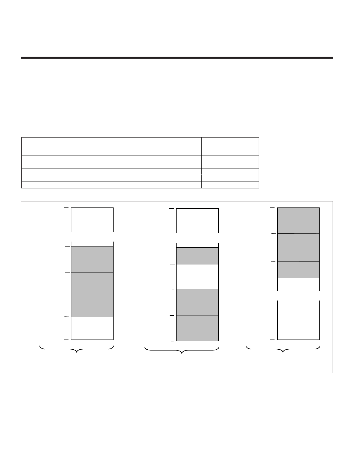
IDM1:0 CMA
1kB SRAM
(OPTIONAL STACK)
8kB SRAM
(ETHERNET BCU)
256–BYTE SRAM
(CAN)
00 0 00DC00h–00DFFFh 00E000h–00FFFFh 00DB00h–00DBFFh
00 1 00DC00h–00DFFFh 00E000h–00FFFFh FFDB00h–FFDBFFh
01 0 002000h–0023FFh 000000h–001FFFh 00DB00h–00DBFFh
01 1 002000h–0023FFh 000000h–001FFFh FFDB00h–FFDBFFh
10 0 FFDC00h–FFDFFFh FFE000h–FFFFFFh 00DB00h–00DBFFh
10 1 FFDC00h–FFDFFFh FFE000h–FFFFFFh FFDB00h–FFDBFFh
High-Speed Microcontroller User’s
IDM1:0 = 10b; CMA = 1
Addressable
External
Memory
000000h
FFFFFFh
FFDC00h
FFDBFFh
FFE000h
FFDFFFh
~
~
~
~
Internal
8kB SRAM
(Ethernet BCU)
Internal
1kB SRAM
(Optional Stack)
256-byte SRAM
(
CAN
)
FFDB00h
FFDAFFh
IDM1:0 = 00b; CMA = 0
(DEFAULT)
Addressable
External
Memory
Addressable
External
Memor
y
000000h
FFFFFFh
00DC00h
00DBFFh
00E000h
00DFFFh
~
~
~
~
Internal
8kB SRAM
(Ethernet BCU)
Internal
1kB SRAM
(Optional Stack)
256-byte SRAM
(
CAN
)
00DB00h
00DAFFh
010000h
00FFFFh
IDM1:0 = 01b; CMA = 0
Addressable
External
Memory
Addressable
External
Memory
000000h
FFFFFFh
002400h
0023FFh
00DB00h
00DAFFh
~
~
~
~
256-byte SRAM
(
CAN
)
002000h
001FFF
h
00DC00h
00DBFFh
Internal
1kB SRAM
(Optional Stack)
Internal
8kB SRAM
(Ethernet BCU)
Maxim Integrated
Guide: Network Microcontroller
Supplement
Internal Data Memory
DS80C400
The DS80C400 incorporates 9472 bytes of internal SRAM memory, in addition to the standard 256-byte scratchpad memory. This additional on-chip SRAM is logically divided into three memory blocks: a 1kB block usable as data memory and extended stack memory,
an 8kB block usable as data memory and Ethernet transmit/receive buffer memory, and a 256-byte block usable as data memory and
CAN controller memory. In order for the 1kB internal SRAM to be used as extended stack memory, the stack address mode (SA) bit
contained in the ACON register, must be set to 1. The logical address location for each block is determined by the settings of the IDM1,
IDM0 bits and the CMA bit, all contained in the MCON (C6h) register. Table 6-1 summarizes the six possible configurations for the three
internal SRAMs, while Figure 6-2 illustrates three data memory map possibilities.
Table 6-1. Internal Data Memory Address Locations
Figure 6-2. Example Data Memory Map Configurations (DS80C400)
98
Page 99

High-Speed Microcontroller User’s
Addressable
External
Data Memory
IRAMD = 1, PRAME = X
Internal 8kB SRAM
(Ethernet BCU)
FFFFFFh
Internal 1kB SRAM
(Optional Stack)
FFE000h
FFDFFFh
FFDC00h
FFDBFFh
FFDB00h
FFDAFFh
000000h
256 Byte SRAM
(CAN)
Addressable
External
Data Memory
Internal 65kB
Data SRAM
IRAMD = 0, PRAME = 0
* This memory should not be
accessed on the DS80C411.
* This memory should not be
accessed on the DS80C411.
Internal 8kB SRAM
(Ethernet BCU)
FFFFFFh
Internal 1kB SRAM
(Optional Stack)
FFE000h
FFDFFFh
FFDC00h
FFDBFFh
FFDB00h
FFDAFFh
010000h
00FFFFh
000000h
010000h
00FFFFh
256 Byte SRAM*
(CAN)
Addressable
External
Data Memory
Internal merged
64kB Data
and Program SRAM
Internal 8kB SRAM
(Ethernet BCU)
Internal 1kB SRAM
(Optional Stack)
256 Byte SRAM*
(CAN)
IRAMD = 0, PRAME = 1
FFFFFFh
FFE000h
FFDFFFh
FFDC00h
FFDBFFh
FFDB00h
FFDAFFh
000000h
Maxim Integrated
Guide: Network Microcontroller
Supplement
DS80C410/DS80C411
Similar to the DS80C400, the DS80C410 and DS80C411 incorporate three internal SRAM memory blocks: a 1kB block usable as data
memory and extended stack memory, a 64kB block usable as data memory and Ethernet transmit/receive buffer memory, and a 256byte block usable as data memory and CAN controller memory. For the 1kB internal SRAM to be used as extended stack memory, the
stack address mode (SA) bit contained in the ACON register must be set to 1. Unlike the DS80C400, the logical addresses of these
blocks are fixed, as follows:
CAN SRAM (256 byte): FFDB00h–FFDBFFh
Data/Extended Stack (1kB) FFDC00h–FFDFFFh
Internal Data memory (64kB) 0000000h–00FFFFh
The 64kB memory block can be enabled or disabled by the Internal RAM Disable bit, IRAMD (MCON1.7). When enabled, the 64kB
memory block appears in the MOVX address space at locations 0000000h–00FFFFh. All MOVX memory operations in that range automatically access internal memory, and no external memory signals (address bus, RD or WR strobes) are active. When disabled, all
MOVX memor
The DS80C410/411 incorporate a new feature that allows the 64kB memory block to be mapped from data into program memory
space. The Program RAM Enable bit, PRAME (MCON1.6) contr
either be located at 0000000h–00FFFFh in data space or program space. This very useful feature allows the designer to create selfmodifying code by using MOVC instructions to read existing code space into the 64kB data memory block, modify it, and then use the
PRAME bit to map the 64kB block back into program memory space. These features are illustrated in Figure 6-3.
y operations over that range are directed onto the external bus and the internal locations are ignored.
ols whether the 64kB memory block, if enabled by the IRAMD bit, will
Figure 6-3. Example Data Memory Map Configurations (DS80C410/DS80C411)
99
Page 100

High-Speed Microcontroller User’s
SIGNAL MULTIPLEX E D (MUX = 0) DEMULTIPLEXED (MU X = 1)
A21 P6.5 P6.5
A20 P6.4 P6.4
A19 P4.7 P4.7
A18 P4.6 P4.6
A17 P4.5 P4.5
A16 P4.4 P4.4
A15 – A8 P2.7–P2.0 P 2.7 –P2.0
ADDRESS
A7– A0 P0.7– P 0 . 0 P7.7–P7 .0
DATA D7–D0 P0.7–P0.0 P0.7–P0.0
CE7 P6.3 P6.3
CE6 P6.2 P6.2
CE5 P6.1 P6.1
CE4 P6.0 P6.0
CE3 P4.3 P4.3
CE2 P4.2 P4.2
CE1 P4.1 P4.1
CHIP ENABLES
CE0 P4.0 P4.0
PCE2 P5.7 P5.7
PCE1 P5.6 P5.6
PCE0 P5.5 P5.5
PERIPHERAL
CHIP ENABLES
— P5.4 P5.4
Maxim Integrated
Guide: Network Microcontroller
Supplement
External Memory Access
The DS80C400 follows the memory interface convention established by the industry standard 80C32/80C52 but with many added
improvements. Most notably, the device incorporates a 24-bit addressing capability that directly supports up to 16MB of program memory and 4MB of data memory. Externally, the memory is accessed through a multiplexed or demultiplexed 22-bit address bus/8-bit data
bus and eight chip-enable signals (active during program memory access) or four peripheral-enable signals (active during data memory access). Multiplexed addressing mode mimics the traditional 8051 memory interface with the address MSB presented on port 2
and the address LSB and data multiplexed on port 0. The multiplexed mode requires an external latch to demultiplex the address LSB
and data. When the MUX pin is pulled high, the address LSB and data are demultiplexed with the address MSB presented on port 2,
the address LSB on port 7, and the data on port 0. The elimination of the demultiplexing latch removes a delay element in the memory timing and can, in some cases, allow the use of slower, less expensive memory devices. Table 6-2 illustrates the locations of the
external memory control signals.
Table 6-2. External Memory Addressing Pin Assignments
Each upper-order address line (A16–A21) and chip or peripheral enable is individually enabled by the P4CNT, P5CNT, and P6CNT registers. Enabling upper-order address lines increases the maximum size of the external memories that can be addressed, and enabling
chips or peripheral enables control the number of external memories that can be addressed. For example, if P4CNT.5-3 are set to 010b,
A17 and A16 are enabled (along with A15–A0), permitting each chip-enable access a maximum memory device size of 218or 256kB.
Note that the desired chip-enable signals must be enabled in order to become active for a defined memory range.
The configurable program/code chip-enable (CEx) and MOVX chip-enable (PCEx) signals issued by the microcontroller are used when
accessing multiple external memory devices. External chip-enable lines are only required if more than one physical block of memory
are used. In the standard 8051 configuration, PSEN is used as the output enable for the program memor
trol the input or output functions of the data (SRAM) device. Typically, the chip enables of the program and data memory devices can
be connected to their active state if only one of each is used. To support a larger amount of memory, however, the microcontroller must
generate chip or data enables to select one of several memory devices. Tables 6-3 through 6-5 demonstrate how to enable various
combinations of high-order addr
ess lines and chip enables.
y device, and RD and WR con-
100
 Loading...