

Page 1

DS4830A
Optical Microcontroller
User’s Guide
Rev 0; 12/13
Maxim Integrated cannot assume responsibility for use of any circuitry other than circuitry entirely embodied in a Maxim Integrated product. No circuit
patent licenses are implied. Maxim Integrated reserves the right to change the circuitry and specifications without notice at any time.
Maxim Integrated Products, Inc. 160 Rio Robles, San Jose, CA 95134 USA 1-408-601-1000
2013 Maxim Integrated Products The Maxim logo and Maxim Integrated are registered trademarks of Maxim Integrated Products, Inc.
Page 2

DS4830A User’s Guide
Contents
SECTION 1 – OVERVIEW .................................................................................................................................................... 11
SECTION 2 – ARCHITECTURE ........................................................................................................................................... 13
2.1 – Instruction Decoding ................................................................................................................................................. 13
2.2 – Register Space ......................................................................................................................................................... 14
2.3 – Memory Types .......................................................................................................................................................... 15
2.3.1 – Flash Memory .................................................................................................................................................... 15
2.3.2 – SRAM Memory ................................................................................................................................................... 15
2.3.3 – Utility ROM ......................................................................................................................................................... 15
2.3.4 – Stack Memory .................................................................................................................................................... 16
2.4 – Program and Data Memory Mapping and A cc ess ................................................................................................... 16
2.4.1 – Program Memory Access .................................................................................................................................. 16
2.4.2 – Program Memory Mapping ................................................................................................................................ 17
2.4.3 – Data Memory Access ......................................................................................................................................... 17
2.4.4 – Data Memory Mapping....................................................................................................................................... 18
2.5 – Data Alignment ......................................................................................................................................................... 22
2.6 – Reset Conditions ...................................................................................................................................................... 22
2.6.1 – Power-On/Brownout Reset ................................................................................................................................ 22
2.6.2 – Watchdog Timer Reset ...................................................................................................................................... 23
2.6.3 – External Reset ................................................................................................................................................... 23
2.6.4 – Internal System Resets ...................................................................................................................................... 24
2.6.5 – Software Reset .................................................................................................................................................. 24
2.7 – Clock Generation ...................................................................................................................................................... 24
SECTION 3 – SYSTEM REGISTER DESCRIPTIONS ......................................................................................................... 25
3.1 – Accumulator Pointer Register (AP, 08h[00h]) .......................................................................................................... 27
3.2 – Accumulator Pointer Control Register (APC, 08h[01h]) ........................................................................................... 27
3.3 – Processor Status Flags Register (PSF, 08h[04h]) ................................................................................................... 27
3.4 – Interrupt and Control Register (IC, 08h[05h]) ........................................................................................................... 28
3.5 – Interrupt Mask Register (IMR, 08h[06h]) .................................................................................................................. 28
3.6 – System Control Register (SC, 08h[08h]) .................................................................................................................. 28
3.7 – Interrupt Identification Register (I IR, 08h[0Bh]) ........................................................................................................ 29
3.8 – Watchdog Control Register (WDCN, 08h[ 0F h]) ....................................................................................................... 29
3.9 – Accumulator n Register (A[n], 09h[ nh]) .................................................................................................................... 29
3.10 – Prefix Register (PFX[n], 0Bh[n] .............................................................................................................................. 29
3.11 – Instruction Pointer Register (IP, 0Ch[00h]) ............................................................................................................ 30
3.12 – Stack Pointer Register (SP, 0Dh[01h]) ................................................................................................................... 30
3.13 – Interrupt Vector Register (IV, 0Dh[02h]) ................................................................................................................. 30
3.14 – Loop Counter 0 Register (LC[0], 0Dh[06h]) ........................................................................................................... 30
3.15 – Loop Counter 1 Register (LC[1], 0Dh[07h]) ........................................................................................................... 30
3.16 – Frame Pointer Offset Register (OFFS, 0Eh[03h]) .................................................................................................. 30
3.17 – Data Pointer Control Register (DP C, 0Eh[04h]) ..................................................................................................... 31
2
Page 3

DS4830A User’s Guide
3.18 – General Register (GR, 0Eh[05h]) ........................................................................................................................... 31
3.19 – General Register Low Byte (GRL, 0Eh[06h]) ......................................................................................................... 31
3.20 – Frame Pointer Base Register (BP, 0E h[07h]) ........................................................................................................ 31
3.21 – General Register Byte-Swapped (GRS, 0Eh[08h] ) ................................................................................................ 32
3.22 – General Register High Byte (GRH, 0E h[09h]) ........................................................................................................ 32
3.23 – General Register Sign Extended Low By te (GRXL, 0Eh[0Ah]) .............................................................................. 32
3.24 – Frame Pointer Register (FP, 0Eh[0Bh]) ................................................................................................................. 32
3.25 – Data Pointer 0 Register (DP[0], 0Fh[03h]) ............................................................................................................. 32
3.26 – Data Pointer 1 Register (DP[1], 0Fh[07h]) ............................................................................................................. 32
SECTION 4 – PERIPHERAL REGISTER DESCRIPTIONS ................................................................................................. 33
4.1 – Module 0 Peripheral Registers ................................................................................................................................. 34
4.2 – Module 1 Peripheral Registers ................................................................................................................................. 35
4.3 – Module 2 Peripheral Registers ................................................................................................................................. 36
4.4 – Module 3 Peripheral Registers ................................................................................................................................. 37
4.5 – Module 4 Peripheral Registers ................................................................................................................................. 38
4.6 – Module 5 Peripheral Registers ................................................................................................................................. 39
SECTION 5 – INTERRUPTS ................................................................................................................................................ 40
5.1 – Servicing Interrupts ................................................................................................................................................... 41
5.2 – Module Interrupt Identification Registers .................................................................................................................. 42
5.3 – Interrupt System Operation ...................................................................................................................................... 43
5.3.1 – Synchronous vs. Asynchronous Int errupt Sources ............................................................................................ 44
5.3.2 – Interrupt Prioritization by Software ..................................................................................................................... 44
5.3.3 – Interrupt Exception Window ............................................................................................................................... 44
SECTION 6 – DIGITAL-TO-ANALOG CONVERTER (DAC) ................................................................................................ 45
6.1 – Detailed Description ................................................................................................................................................. 45
6.1.1 – Reference Selection .......................................................................................................................................... 46
6.2 – DAC Register Descriptions ....................................................................................................................................... 46
6.2.1 – DAC Configuration Register (DACCFG) ............................................................................................................ 46
6.2.2 – DAC Data Registers (DACD0-DACD7) ............................................................................................................. 47
6.2.3 – Reference Pin Configuration Register (RPCFG) .............................................................................................. 47
6.3 – DAC Code Examples ................................................................................................................................................ 47
SECTION 7 – ANALOG-TO-DIGITAL CONVERTER (ADC) ................................................................................................ 48
7.1 – Detailed Description ................................................................................................................................................. 48
7.1.1 – ADC Controller ................................................................................................................................................... 48
7.1.2 – ADC Conversion Sequencing ............................................................................................................................ 49
7.1.3 – Internal Die Temperature Conversion ................................................................................................................ 50
7.1.4 – Sample and Hold Conversion ............................................................................................................................ 51
7.1.5 – ADC Frame Sequence ....................................................................................................................................... 51
7.1.6 – ADC Reference .................................................................................................................................................. 51
7.1.7 – ADC Conversion Time ....................................................................................................................................... 52
7.1.8 – Location Override ............................................................................................................................................... 53
7.1. 9 – Averaging .......................................................................................................................................................... 53
3
Page 4

DS4830A User’s Guide
7.1.10 – ADC Data Reading .......................................................................................................................................... 54
7.1.11 – ADC Interrupts ................................................................................................................................................. 54
7.1.12 – ADC Internal Offset .......................................................................................................................................... 55
7.1.13 – DAC External Reference Pins (REFI NA and REFINB) as ADC Channels ...................................................... 55
7.1.14 – Fast Conversion Mode (ADST.E NABLE_2X) .................................................................................................. 55
7.2 – ADC Register Descriptions ....................................................................................................................................... 56
7.2.1 – ADC Control Register (ADCN) ........................................................................................................................... 56
7.2.2 – ADC Status Register (ADST) ............................................................................................................................. 57
7.2.3 – PIN Select Register (PINSEL) ........................................................................................................................... 57
7.2.4 – ADC Status Register (ADST1) .......................................................................................................................... 58
7.2.5 – ADC Address Register (ADADDR) .................................................................................................................... 58
7.2.6 – ADC Data and Configuration Registe r (A DDATA) ............................................................................................. 58
7.2.7 – Reference Pin Configuration Register (RPCFG ) ............................................................................................... 60
7.2.8 – Temperature Control Register (TEMP CN ) ....................................................................................................... 61
7.2.9 – Average and Reference Control Register (REFAVG) ..................................................................................... 61
7.2.10 – ADC Voltage Offset Register (ADVOFF) ......................................................................................................... 62
7.2.11 – ADC Voltage Scale Trim Registers (AD CG1, ADCG2, ADCG3 and ADCG4) ................................................ 62
7.3 – ADC Code Examples ................................................................................................................................................ 63
SECTION 8 – SAMPLE AND HOLD ..................................................................................................................................... 65
8.1 – Detailed Description ................................................................................................................................................. 65
8.1.1 – Operation ........................................................................................................................................................... 65
8.1.2 – Fast Mode Operation ......................................................................................................................................... 66
8.1.3 – Sampling Control ............................................................................................................................................... 67
8.1.4 – Pin Capacitance Discharge ............................................................................................................................... 68
8.1.5 – Sample and Hold Data Reading ........................................................................................................................ 69
8.1.6 – Sample and Hold Interrupts ............................................................................................................................... 69
8.2 – Sample and Hold Register Descriptions ................................................................................................................... 70
SECTION 9 – QUICK TRIP (FAST COMPARATOR) ........................................................................................................... 73
9.1 – Detailed Description ................................................................................................................................................. 73
9.1.1 – Quick Trip List Sequencing ................................................................................................................................ 74
9.1.2 – Operation ........................................................................................................................................................... 74
9.1.3 – Setting Quick Trip Thresholds ........................................................................................................................... 75
9.1.4 – Quick Trip Interrupts .......................................................................................................................................... 76
9.2 – Quick Trip Register Descriptions .............................................................................................................................. 77
SECTION 10 – I2C-COMPATIBLE MASTER INTERFACE .................................................................................................. 81
10.1 – Detailed Description ............................................................................................................................................... 81
10.1.1 – Description of Master I2C Interface .................................................................................................................. 81
10.1.2 – Default Operation ............................................................................................................................................. 81
10.1.3 – I2C Clock Generation ....................................................................................................................................... 81
10.1.4 – Timeout ............................................................................................................................................................ 82
10.1.5 – Generating a START ....................................................................................................................................... 83
10.1.6 – Generating a STOP ......................................................................................................................................... 85
4
Page 5

DS4830A User’s Guide
10.1.7 – Transmitting a Slave Address .......................................................................................................................... 85
10.1.8 – Transmitting Data ............................................................................................................................................. 85
10.1.9 – Receiving Data ................................................................................................................................................. 87
10.1.10 – I2C Master Clock Stretching ........................................................................................................................... 88
10.1.11 – Resetting the I2C Master Controller ............................................................................................................... 88
10.1.12 – Alternate Location .......................................................................................................................................... 89
10.1.13 – Operation as a Slave ..................................................................................................................................... 89
10.1.14 – GPIO .............................................................................................................................................................. 89
10.2 – I2C Master Controller Register Description ............................................................................................................ 90
SECTION 11 – I2C-COMPATIBLE SLAVE INTERFACE ...................................................................................................... 94
11.1 – Detailed Description ............................................................................................................................................... 95
11.1.1 – Default Operation ............................................................................................................................................. 95
11.1.2 – Slave Addresses .............................................................................................................................................. 95
11.1.3 – I2C START Detection ....................................................................................................................................... 95
11.1.4 – I2C STOP Detection ......................................................................................................................................... 95
11.1.5 – Slave Address Matching .................................................................................................................................. 95
11.1.6 – Advanced Mode Operation RX FIFO and TX Pages ....................................................................................... 97
11.1.7 – Transmitting Data ............................................................................................................................................. 98
11.1.8 – Receiving Data ............................................................................................................................................... 100
11.1.9 – Clock Stretching ............................................................................................................................................. 100
11.1.10 – SMBus Timeout ........................................................................................................................................... 102
11.1.11 – Resetting the I2C Slave Controller ............................................................................................................... 102
11.2 – I2C Slave Controller Register Description ............................................................................................................ 103
SECTION 12 – SERIAL PERIPHERAL INTERFACE (SPI) ................................................................................................ 111
12.1 – Serial Peripheral Interface (SPI) Detailed Description ......................................................................................... 111
12.1.1 – SPI Transfer Formats ........................................................................................................................................ 111
12.1.2 – SPI Character Lengths ...................................................................................................................................... 113
12.2 – SPI System Errors ................................................................................................................................................ 113
12.2.1 – Mode Fault ......................................................................................................................................................... 113
12.2.2 – Receive Overrun ................................................................................................................................................ 113
12.2.3 – Write Collision While Busy ................................................................................................................................ 114
12.3 – SPI Interrupts ........................................................................................................................................................ 114
12.4 – SPI Master ............................................................................................................................................................ 114
12.4.1 – SPI Transfer Baud Rates .................................................................................................................................. 114
12.4.2 – SPI Master Operation ........................................................................................................................................ 114
12.4.3 – SPI Master Register Descriptions ..................................................................................................................... 116
12.5 – SPI Slave .............................................................................................................................................................. 118
12.5.1 – SPI Slave Select ............................................................................................................................................ 118
12.5.2 – SPI Transfer Baud Rates ............................................................................................................................... 118
12.5.3 – SPI Slave Operation ...................................................................................................................................... 118
12.5.4 – SPI Slave Register Descriptions ....................................................................................................................... 119
5
Page 6

DS4830A User’s Guide
SECTION 13 – 3-WIRE ....................................................................................................................................................... 121
13.1 – Detailed Description ............................................................................................................................................. 121
13.1.1 – Operation ....................................................................................................................................................... 121
13.2 – 3-Wire Register Descriptions ................................................................................................................................ 123
SECTION 14 – PWM .......................................................................................................................................................... 124
14.1 – Detailed Description ............................................................................................................................................. 124
14.1.1 – PWMCN and PWMDATA SFRs .................................................................................................................... 124
14.1.2 – PWMSYNC SFR ............................................................................................................................................ 125
14.2 – Individual PWM Channel Operation ..................................................................................................................... 126
14.2.1 – Duty Cycle Register (DCYCn) ....................................................................................................................... 126
14.2.2 – PWM Configuration Register (PWM CFGn) ................................................................................................... 127
14.2.3 – PWM DELAY Register (PWMDLYn) .............................................................................................................. 131
14.3 – PWM Output Register Descriptio ns ...................................................................................................................... 132
14.4 – PWM Output Code Examples .............................................................................................................................. 137
SECTION 15 – GENERAL-PURPOSE INPUT/OUTPUT (GPIO) PINS ............................................................................. 138
15.1 – Overview ............................................................................................................................................................... 138
15.2 – GPIO Port Register Descriptions .......................................................................................................................... 141
15.2.1 – GPIO Direction Register Port (PD0, P D1, P D2, and PD6) ............................................................................ 141
15.2.2 – GPIO Output Register Port (PO0, PO1, PO2, and PO6)............................................................................... 141
15.2.3 – GPIO Input Register for Port (PI0, PI1, PI2, and PI6) ................................................................................... 141
15.2.4 – GPIO Port External Interrupt Edge Select Register (EIES0, EIES1, EIES2, and EIES6) ............................. 141
15.2.5 – GPIO Port External Interrupt Flag Register (EIF0, EIF1, EIF2, and EIF6) .................................................... 142
15.2.6 – GPIO Port External Interrupt Enable Register (EIE0, EIE1, EIE2, and EIE6) ............................................... 142
15.3 – GPIO Code Example ............................................................................................................................................ 142
15.3.1 – GPIO Pin as Output ....................................................................................................................................... 142
15.3.2 – GPIO High-Impedance Input ......................................................................................................................... 142
15.3.3 – GPIO Weak Pullup Input ................................................................................................................................ 142
15.3.4 – GPIO Open-Drain Output .............................................................................................................................. 142
SECTION 16 – GENERAL-PURPOSE TIMERS ................................................................................................................ 143
16.1 – Detailed Description ............................................................................................................................................. 143
16.1.1 – Timer Modes .................................................................................................................................................. 143
16.1.2 – Clock Selection .............................................................................................................................................. 144
16.1.3 – Timer Clock Prescaler ................................................................................................................................... 144
16.2 – Timer Register Descriptions ................................................................................................................................. 145
SECTION 17 – SUPPLY VOLTAGE MONITOR (SVM)...................................................................................................... 147
SECTION 18 – HARDWARE MULTIPLIER MODULE ....................................................................................................... 148
18.1 – Hardware Multiplier Organization ......................................................................................................................... 148
18.2 – Hardware Multiplier Controls ................................................................................................................................ 148
18.3 – Register Output Selection .................................................................................................................................... 149
18.3.1 – Signed-Unsigned Operand Selection ............................................................................................................ 149
18.3.2 – Operand Count Selection .............................................................................................................................. 149
18.4 – Hardware Multiplier Operations ............................................................................................................................ 149
6
Page 7

DS4830A User’s Guide
18.4.1 – Accessing the Multiplier ................................................................................................................................. 149
18.5 – Hardware Multiplier Peripheral Registers ............................................................................................................. 151
18.6 – Hardware Multiplier Examples .............................................................................................................................. 155
SECTION 19 – WATCHDOG TIMER ................................................................................................................................. 156
19.1 - Overview ............................................................................................................................................................... 156
19.2 – Watchdog Timer Description ................................................................................................................................ 156
19.2.1 – Watchdog Timer Interrupt Operation ............................................................................................................. 157
19.2.2 – Watchdog Timer Reset Operation ................................................................................................................. 157
19.2.3 – Watchdog Timer Applications ........................................................................................................................ 157
SECTION 20 – TEST ACCESS PORT (TAP) ..................................................................................................................... 159
20.1 – TAP Controller ...................................................................................................................................................... 160
20.2 – TAP State Control ................................................................................................................................................. 161
20.2.1 – Test-Logic-Reset ............................................................................................................................................ 161
20.2.2 – Run-Test-Idle ................................................................................................................................................. 161
20.2.3 – IR-Scan Sequence ......................................................................................................................................... 161
20.2.4 – DR-Scan Sequence ....................................................................................................................................... 162
20.3 – Communication via TAP ....................................................................................................................................... 162
20.3.1 – TAP Communication Examples – IR-Scan and DR-Scan ............................................................................. 163
SECTION 21 – IN-CIRCUIT DEBUG MODE ...................................................................................................................... 165
21.1 – Background Mode Operation ............................................................................................................................... 166
21.1.1 – Breakpoint Registers ..................................................................................................................................... 167
21.1.2 – Using Breakpoints .......................................................................................................................................... 169
21.2 – Debug Mode ......................................................................................................................................................... 170
21.2.1 – Debug Mode Commands ............................................................................................................................... 170
21.2.2 – Read Register Map Command Host-R O M Interaction .................................................................................. 172
21.2.3 – Single Step Operation (Trace) ....................................................................................................................... 173
21.2.4 – Return ............................................................................................................................................................ 174
21.2.5 – Debug Mode Special Considerations ............................................................................................................ 174
21.3 – In-Circuit Debug Peripheral Registers .................................................................................................................. 175
SECTION 22 – IN-SYSTEM PROGRAMMING .................................................................................................................. 179
22.1 – Detailed Description ............................................................................................................................................. 179
22.1.1 – Password Protection ...................................................................................................................................... 180
22.1.2 – Entering JTAG Bootloader ............................................................................................................................. 180
22.1.3 – Entering I2C Bootloader ................................................................................................................................. 181
22.1.4 – I2C Bootloader Disable ................................................................................................................................... 181
22.2 – Bootloader Operation ........................................................................................................................................... 182
22.2.1 – JTAG Bootloader Protocol ............................................................................................................................. 182
22.2.2 – I2C Bootloader Protocol ................................................................................................................................. 183
22.3 – Bootloader Commands ......................................................................................................................................... 184
22.3.1 – Command 00h – No Operation ...................................................................................................................... 184
22.3.2 – Command 01h – Exit Loader ......................................................................................................................... 184
22.3.3 – Command 02h – Master Erase ...................................................................................................................... 184
7
Page 8

DS4830A User’s Guide
22.3.4 – Command 03h – Password Match ................................................................................................................. 185
22.3.5 – Command 04h – Get Status .......................................................................................................................... 185
22.3.6 – Command 05h – Get Supported Commands ................................................................................................ 186
22.3.7 – Command 06h – Get Code Size .................................................................................................................... 186
22.3.8 – Command 07h – Get Data Size ..................................................................................................................... 186
22.3.9 – Command 08h – Get Loader Version ............................................................................................................ 186
22.3.10 – Command 09h – Get Utility ROM Version ................................................................................................... 186
22.3.11 – Command 10h – Load Code ........................................................................................................................ 187
22.3.12 – Command 11h – Load Data ......................................................................................................................... 187
22.3.13 – Command 20h – Dump Code ...................................................................................................................... 187
22.3.14 – Command 21h – Dump Data ....................................................................................................................... 188
22.3.15 – Command 30h – CRC Code ........................................................................................................................ 188
22.3.16 – Command 31h – CRC Data ......................................................................................................................... 188
22.3.17 – Command 40h – Verify Code ...................................................................................................................... 189
22.3.18 – Command 41h – Verify Data ....................................................................................................................... 189
22.3.19 – Command 50h – Load and Verify Code ...................................................................................................... 189
22.3.20 – Command 51h – Load and Verify Data ....................................................................................................... 189
22.3.21 – Command E0h – Code Page Erase ............................................................................................................ 189
SECTION 23 – PROGRAMMING ....................................................................................................................................... 190
23.1 – Addressing Modes ................................................................................................................................................ 190
23.2 – Prefixing Operations ............................................................................................................................................. 190
23.3 – Reading and Writing Registers ............................................................................................................................. 191
23.3.1 – Loading an 8-Bit Register with an Immediate Value ...................................................................................... 191
23.3.2 – Loading a 16-Bit Register with a 16-Bit Immediate Value ............................................................................. 191
23.3.3 – Moving Values Between Registers of the Same Size ................................................................................... 191
23.3.4 – Moving Values Between Registers of Different Sizes ................................................................................... 191
23.4 – Reading and Writing Register Bits ....................................................................................................................... 192
23.5 – Using the Arithmetic and Logic Unit ..................................................................................................................... 193
23.5.1 – Selecting the Active Accumulator .................................................................................................................. 193
23.5.2 – Enabling Auto-Increment and Auto-Decrement ............................................................................................. 193
23.5.3 – ALU Operations Using the Active A ccu m ul ator and a Source ...................................................................... 195
23.5.4 – ALU Operations Using Only the Acti ve Accumulator ..................................................................................... 195
23.5.5 – ALU Bit Operations Using Only the A ct i ve Accumulator ............................................................................... 195
23.5.6 – Example: Adding Two 4-Byte Numbe rs Using Auto-Increment ..................................................................... 195
23.6 – Processor Status Flag Operations ....................................................................................................................... 195
23.6.1 – Sign Flag ........................................................................................................................................................ 195
23.6.2 – Zero Flag ........................................................................................................................................................ 196
23.6.3 – Equals Flag .................................................................................................................................................... 196
23.6.4 – Carry Flag ...................................................................................................................................................... 196
23.6.5 – Overflow Flag ................................................................................................................................................. 197
23.7 – Controlling Program Flow ..................................................................................................................................... 197
23.7.1 – Obtaining the Next Execution Address .......................................................................................................... 197
8
Page 9

DS4830A User’s Guide
23.7.2 – Unconditional Jumps ..................................................................................................................................... 197
23.7.3 – Conditional Jumps ......................................................................................................................................... 198
23.7.4 – Calling Subroutines ........................................................................................................................................ 198
23.7.5 – Looping Operations........................................................................................................................................ 198
23.7.6 – Conditional Returns ....................................................................................................................................... 199
23.8 – Handling Interrupts ............................................................................................................................................... 199
23.8.1 – Conditional Return from Interr upt .................................................................................................................. 200
23.9 – Accessing the Stack ............................................................................................................................................. 200
23.10 – Accessing Data Memory .................................................................................................................................... 201
SECTION 24 – INSTRUCTION SET .................................................................................................................................. 203
SECTION 25 – UTILITY ROM ............................................................................................................................................ 231
25.1 – Overview ............................................................................................................................................................... 231
25.2 – In-Application Programming Functions ................................................................................................................ 232
25.2.1 – UROM_flashWrite .......................................................................................................................................... 232
25.2.2 – UROM_flashErasePage ................................................................................................................................ 232
25.3 – Data Transfer Functions ....................................................................................................................................... 233
25.3.1 – UROM_moveDP0 .......................................................................................................................................... 233
25.3.2 – UROM_moveDP0inc...................................................................................................................................... 233
25.3.3 – UROM_moveDP0dec .................................................................................................................................... 234
25.3.4 – UROM_moveDP1 .......................................................................................................................................... 234
25.3.5 – UROM_moveDP1inc...................................................................................................................................... 234
25.3.6 – UROM_moveDP1dec .................................................................................................................................... 235
25.3.7 – UROM_moveBP ............................................................................................................................................ 235
25.3.8 – UROM_moveBPinc ........................................................................................................................................ 235
25.3.9 – UROM_moveBPdec....................................................................................................................................... 236
25.3.10 – UROM_copyBuffer ....................................................................................................................................... 236
25.4 Special Functions .................................................................................................................................................... 237
25.4. 1 – UROM_copyWord ......................................................................................................................................... 237
25.4. 2 – Software Reset ............................................................................................................................................. 237
25.5 – Utility ROM Examples ........................................................................................................................................... 238
25.5.1 – Reading Constant Word Data from Flash ...................................................................................................... 238
25.5.2 – Reading Constant Byte Data from Flash (Indirect Function Call) .................................................................. 238
SECTION 26 – MISCELLANEOUS .................................................................................................................................... 239
26.1 – Overview ............................................................................................................................................................... 239
26.2 – CRC8 .................................................................................................................................................................... 239
26.2.1 – CRC Data In (CRC8IN) .................................................................................................................................. 239
26.2.2 – CRC Data Out (CRC8OUT) ........................................................................................................................... 239
26.2.3 – Example ......................................................................................................................................................... 239
26.3 – Software Interrupts ............................................................................................................................................... 239
26.3.1 – User Interrupt Register (USER_INT) ............................................................................................................. 240
26.4 – General-Purpose Registers .................................................................................................................................. 240
26.4.1 – General-Purpose Register ............................................................................................................................. 240
9
Page 10

DS4830A User’s Guide
26.5 – Device Number and I
26.5.1 – Device Number Register (DEV_NUM)........................................................................................................... 240
2
C Bootloader Address Disable .......................................................................................... 240
10
Page 11

DS4830A User’s Guide
SECTION 1 – OVERVIEW
The DS4830A optical microcontroller is a low-power, 16-bit microcontroller with a unique peripheral set supporting a wide
variety of optical transceiver controller applications. It provides a complete optical control, calibration, and monitor
solution. The DS4830A is based on the high-performance, 16-bit, reduced instruction set computing (RISC) architecture
with on-chip flash program memory and SRAM data memory.
The resources and features that the DS4830A p rovides for monitoring and controlling an optical syst em i nclude the
following:
16-Bit Low-Power Microcontroller
400kHz I
32KWords Flash Program Memory
2KWords Data RAM
32-Level Hardware Stack
13-Bit ADC with a 26 Input Mux
10 PWM Channels
10-Bit Fast Comparator with 16 Input Mux
Two Independent Sample and Hold (S/H)
Fast Internal Die Temperature Sensors with Av eraging Option
12-Bit, 8 Voltage DAC Channels Selectable Internal or External Reference Option
Serial Interfaces
Dual Hardware Multiplier Unit
Two 16-Bit Timers with Synchronous and Compare Modes
Watchdog Timer
Maskable Interrupt Sources
Brownout Monitor
31 GPIO pins
Supply Voltage Monitoring
Internal 20MHz Oscillator, CPU Core Frequency 10MHz
Included ROM Routines that allow Bootloading and In-Applicati on Programming of Flash Memory
In-System Debugging
Four Software Interrupts
Fast Hardware CRC-8 for Packet Error Checking (PEC)
2
C-Compatible Slave Communication Interface
• Four User-Programmable Slave Addresses
• 8-Byte Transmit Page for Each Slave Address
• 8-Byte Receive Page Shared Between All Slave A ddresses
• 16 Single or 8 Differential Mode ADC Channels
• Four User-Selectable Gains for Individual Channel
• V
, Internal Reference, and DAC External References Measurement
DD
• ADC Samples Averaging Options
• Pulse Spreading Using Delta-Sigma Algorithm
• PWM Output Synchronization
• User-Selectable 7- to 16-Bit Resolution
• 1MHz Switching Using 133MHz External Cl ock
• Single and Differential Mode
• Low and High Threshold Configurations
• 3.2µs Conversion Time per Channel
• Single, Fast, and Dual Mode Operation
• Internal and External Trigger Option
• Pin Discharge
• S/H Samples Averaging Options
• SPI Master and Slave Interface
• 400kHz I
2
C-Compatible Master with Alternate Lo cat ion Option
• 3-Wire Master Interface
11
Page 12
DS4830A User’s Guide
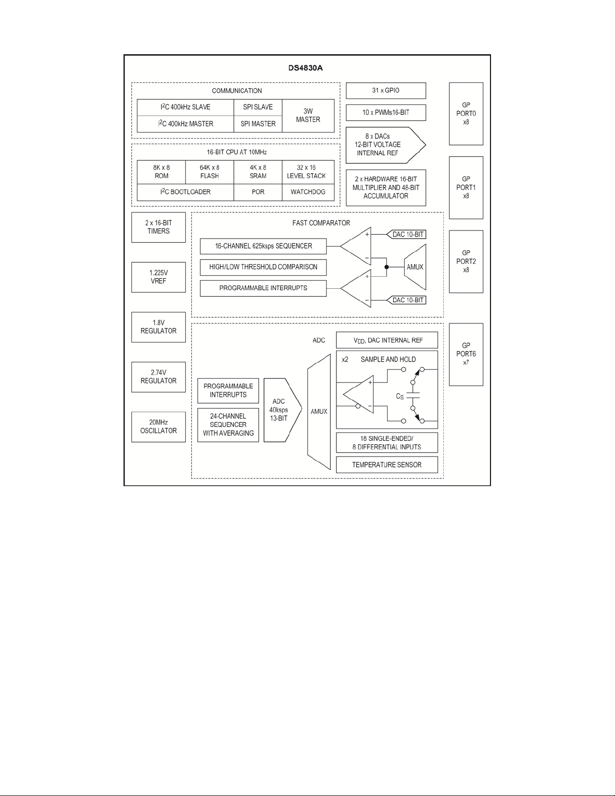
Figure 1-1: DS4830A Block Diagram
This document is provided as a supplement to the DS4830A IC data sheet. This user’s guide provides the information
necessary to develop applications using the DS4830A. All electrical and timing specifications, pin descriptions, package
information, and ordering information can be found in the DS4830A IC data sheet.
12
Page 13

DS4830A User’s Guide
FORMAT DESTINATION SOURCE
s sd
f s s
s s s sd d d d
d d
SECTION 2 – ARCHITECTURE
The DS4830A contains a low-cost, high-performance microcontroller with flash memory. It is structured on a highly
advanced, 16-accumulator-based, 16-bit RISC architecture. Fetch and execution operations are completed in one cycle
without pipelining, since the instruction contains both the opcode and data. The highly efficient core is supported by 16
accumulators and a 32-level hardware stack, en abl i ng fast subroutine calling and task switching.
Data can be quickly and efficiently manipulated with three internal data pointers. Two of these data pointers, DP0 and
DP1, are stand-alone 16-bit pointers. The third data pointer, Frame Pointer, is composed of a 16-bit base pointer (BP) and
an 8-bit offset register (OFFS). All three pointers support post-increment/decrement functionality for read operations and
pre-increment/decrement for write operations. For the Frame Pointer (FP=BP[OFFS]), the increment/decrement operation
is executed on the OFFS register and does not affect the base pointer. Multiple data pointers allow more than one
function to access data memory without hav i ng to save and restore data pointers each time.
Stack functionality is provided by dedicated memory with a 16-bit width and a depth of 32. An on-chip memory
management unit (MMU) allows logical remapping of the program and data spaces, and thus facilitates in-system
programming and fast access to data tables, arrays, and constants located in flash memory.
This section provides details on the following topics.
1. Instruction decoding
2. Register space
3. Memory types
4. Program and data memory mapping and access
5. Data alignment
6. Reset conditions
7. Clock generation
2.1 – Instruction Decoding
The DS4830A uses the standard 16-bit core instruction set, which is described in the Instruction Set section. Every
instruction is encoded as a single 16-bit word. The inst ruction word format is shown in Figure 2-1.
Figure 2-1: Instruction Word Format
• Bit 15 (f) indicates the format for the source field of the instruction as follows:
o If f equals 0, the instruction is an immediate source instruction. The source field represents an immediate
8-bit value.
o If f equals 1, the instruction is a register source instruction. The source field represents the register that
the source value will be read from.
• Bits 14 to 8 (ddddddd) represent the destination for the transfer. This value always represents a destination
register. The lower four bits contain the module specifier and the upper three bits contain the register index in
that module.
• Bits 7 to 0 (ssssssss) represent the source for the transfer. Depending on the value of the format field, this can
either be an immediate value or a source register. If this field represents a register, the lower four bits contain the
module specifier and the upper four bits contain the register index in that module.
This instruction word format presents the f oll owing limitations.
1. There are 32 registers per register module, but only four bits are allocated to designate the source register and
only three bits are allocated to designat e the destination register.
2. The source field only provides 8 bits of data for an immediate value; however a 16-bit immediate value may be
required.
The DS4830A uses a prefix register (PFX) to address these limitations. The prefix register provides the additional bits
required to access all 32 register within a module. The prefix register also provides the additional 8 bits of data required
to make a 16-bit immediate data source. The data that is written to the prefix register survives for only one clock cycle.
This means the write to the prefix register must occur immediately prior to the instruction requiring the prefix register. The
prefix register is cleared to zero after one cycle so it will not affect any other instructions. The write to the prefix register is
13
Page 14

DS4830A User’s Guide
done automatically by the assembler and requires one additional execution cycle. So, while most instructions execute in
a single cycle, two cycles are needed for i nst ructions that require the prefix register.
The architecture of the DS4830A is transport-triggered. This means that writing to or reading from certain register
locations will also cause side effects to occur. These side effects form the basis of the DS4830A’s higher level opcodes,
such as ADDC, OR, and JUMP. While these opcodes are actually implemented as MOVE instructions between certain
register locations, the encoding is handled by the assembler and need not be a concern to the programmer. The unused
"empty" locations in the System Register Modules a re used for these higher level opcodes.
The instruction set is designed to be highly orthogonal. All arithmetic and logical operations that use two registers can use
any register along with the accumulator. Data can be transferred between any two register s in a single instruction.
2.2 – Register Space
The DS4830A provides a total of 13 register modules broken up into two different groups. These groupings are
descriptive only, as there is no difference between accessing the two register groups from a programm ing perspective.
The two groups are:
1. System Registers: These are modules 8h, 9h, and Bh through Fh. The System Registers in the DS4830A are
used to implement higher level opcodes as well as the following common system features.
• 16-bit ALU and associated status flags (zero, equals, carry, sign, overflow)
• 16 working accumulator registers, each 16-bit, along with associated control registers
• Instruction pointer
• Registers for interrupt control, handling, and ide ntification
• Auto-decrementing Loop Counters for fast, compact looping
• Two Data Pointer registers and a Frame Pointer for data memory access
2. Peripheral Registers: These are the lower six modules (Modules 0h through 5h). The Peripheral Registers in the
DS4830A are used for functiona lities such as ADC, Fast Comparator, DAC, PWM Outputs, Timers, Sample and
Hold, 3-Wire, I
used to implement opcodes.
Each System Register module has 16 registers, while each Peripheral Register module has 32 registers. The number of
cycles required to access a particular register depends upon the register’s index within the module. The access times
based upon the register index are grouped as foll ows:
• The first eight registers (index 0h to 7h) in each module may be read from or written to in a single cycle
• The second eight registers (index 8h to 0Fh) may be read from in a single cycle and written to in two cycles (by
using the prefix register PFX).
• The last sixteen registers (10h to 1Fh) in Peripheral Register modules may be read or written in two cycles
(always requiring use of the prefix register PFX).
Registers may be 8 or 16 bits in length. Some registers may contain reserved bits. The user should not write to any
reserved bits. Data transfers between re gist ers of different sizes are handled as shown in Table 2-1.
• If the source and destination registers are bot h 8 bi ts wide, data is copied bit to bit.
• If the source register is 8 bits wide and the destination register is 16 bits wide, the data from the source register is
transferred into the lower 8 bits of the destination register. The upper 8 bits of the destination register are set to
the current value of the prefix register; this value is normally zero, but it can be set to a different value by the
previous instruction if needed. The prefix register reverts back to zero after one cycle, so this must be done by the
instruction immediately before the one that will be using the value.
• If the source register is 16 bits wide and the destination register is 8 bits wide, the lower 8 bits of the source are
transferred to the destination register.
• If both registers are 16 bits wide, data is copied bit to bit.
The above rules apply to all data movements between defined registers. Data transfer to/from undefined register locations
has the following behavior:
• If the destination is an undefined register, the MOVE is a dummy operation but may trigger an underlying
operation according to the source register (e.g. , @DPn--).
• If the destination is a defined register and the source is undefined, the source data for the transfer will depend
upon the source module width. If the source is from a module containing 8-bit or 8-bit and 16-bit source registers,
2
C Master and Slave, SPI Master and Slave, 31-GPIO pins, etc. The Peripheral Registers are not
14
Page 15

DS4830A User’s Guide
SOURCE REGISTER
SIZE (BITS)
DESTINATION REGISTER SIZE
(BITS)
PREFIX
SET?
DESTINATION SET TO VALUE
HIGH 8 BITS
LOW 8 BITS
8
8
X — Source [7:0] 8 16
No
00h
Source [7:0] 8 16
Yes
PFX [7:0]
Source [7:0]
16
8
X — Source [7:0]
16
16
X
Source [15:8]
Source [7:0]
the source data will be equal to the prefix data as the upper 8 bits and 00h as the lower 8 bits. If the source is
from a module containing only 16-bit source registers, 0000h source data is used for the transfer.
Table 2-1. Register-to-Register Transfer Operations
2.3 – Memory Types
In addition to the internal register space, the DS4830A incorporates the following memory types:
• 32KWords of flash memory
• 4KWords of utility ROM contain a debugger and program loader
• 2KWords of SRAM
• 32-level hardware stack for storage of program return addresses
The memory on the DS4830A is organized according to Harvard architecture. This means that there are separate busses
for both program and data memory. Stack memory i s also separate and is accessed through a dedicated registe r set.
2.3.1 – Flash Memory The DS4830A contains 32KWords (32K x 16) of flash memory. The flash memory begins at address 0000h and is contiguous through word address 7FFFh. The flash memory can also be used for storing lookup tables and other nonvolatile data.
The incorporation of flash memory allows the contents of the flash memory to be upgraded in the field, either by the
application or by one of the bootloaders (JTAG or I
that are provided by the utility ROM. See the Utility ROM and In-System Programming sections for more detail s.
2.3.2 – SRAM Memory
The DS4830A contains 2KWords (2K x 16) of SRAM memory. The SRAM memory address begins at address 0000h and
is contiguous through word address 07FFh. The contents of the SRAM are indeterminate after power-on reset, but are
maintained during non-POR resets.
When using the in-circuit debugging features, the highest 19 bytes of the SRAM must be reserved for saved state storage
and working space for the debugging routines. If in-circuit debug is not used, the entire 2KWords of SRAM is available for
application use.
2.3.3 – Utility ROM
The utility ROM is a 4kWord segment of memory. The utility ROM memory address begins at word address 8000h and is
contiguous through word address 8FFFh. The utility ROM is programmed at the factory and cannot be modified. The
utility ROM provides the following system utility functions:
• Reset vector (not user code reset vector)
• In-system programming (bootstrap loader) over JTAG or I
• In-circuit debug routines
• Routines for in-application flash programming
Following any reset, the DS4830A automatically starts execution at the Reset Vector which is address 8000h in the utility
ROM. The ROM code determines whether the program execution should immediately jump to the start of application code
(flash address 0000h), or to one of the special routines mentioned. Routines within the utility ROM are firmwareaccessible and can be called as subroutines by the application software. See the Utility ROM, In-System Programming,
and In-Circuit Debug sections for more information on the routines provided by the utility ROM.
2
C). Writing to flash memory must be done indirectly by using routines
2
C-compatible interfaces
15
Page 16

DS4830A User’s Guide
2.3.4 – Stack Memory
A 16-bit, 32-level on-chip stack provides storage for program return addresses and temporary storage of system registers.
The stack is used automatically by the processor when the CALL, RET, and RETI instructions are executed, and when an
interrupt is serviced. The stack can also be used explicitly to store and retrieve data by using the @SP- - source, @++SP
destination, or the PUSH, POP, and POPI instructions. The POPI instruction acts identically to the POP instruction except
that it additionally clears the INS bit.
The width of the stack is 16 bits to accommodate the instruction pointer size. On reset, the stack pointer SP initializes to
the top of the stack (1Fh). The CALL, PUSH, and interrupt vectoring operations first increment SP and then store a value
at @SP. The RET, RETI, POP, and POPI operations first retrieve the value at @SP and then decrement SP.
The stack memory is initialized to indeterminate values upon reset or power-up. Stack memory is dedicated for stack
operations only and cannot be accessed by the DS4830A program or data busses.
When using the in-circuit debugging features, one word of the stack must be reserved for the debugging routines. If incircuit debug is not used, the entire stack is available for application use.
2.4 – Program and Data Memory Mapping and Access
The memory on the DS4830A is implemented using Harvard architecture, with separate busses for program and data
memory. The Memory Management Unit (MMU) allows the DS4830A to also support a pseudo-Von Neumann memory
map. The pseudo Von Neumann memory map allows each of the memory segments (flash, SRAM, and utility ROM) to
be logically mapped into a single contiguous memory map. This allows all of the memory segments to be accessed as
both program and memory data. The pseudo-Von Neumann memory map provides the following adv antages:
• Program execution can occur from the flash, SRA M , or utility ROM memory segments.
• The SRAM and flash memory segments can both be used for data memory.
Using the pseudo-Von Neumann memory map does have one restriction. This restriction is that a particular memory
segment cannot be simultaneously accessed a s both program and data memory.
2.4.1 – Program Memory Access
The instructions that the DS4830A is executing reside in what is defined as the program memory. The MMU fetches the
instructions using the program bus. The Instruction Pointer (IP) register designates the program memory address of the
next instruction to fetch. The Instruction Pointer is read/write accessible by the user software. A write to the Instruction
Pointer will force program flow to the new address on the next cycle following the write. The content of the Instruction
Pointer will be incremented by 1 automatically after each fetch operation. From an implementation perspective, system
interrupts and branching instructions simply change the contents of the Instruction Pointer and force the opcode to fetch
from a new program location.
16
Page 17
DS4830A User’s Guide
2K * 16
SRAM
16K * 16
FLASH
(SEGMENT 0)
4K * 16
UROM
PROGRAM
SPACE
16K * 16
FLASH
(SEGMENT 1)
0000h
3FFFh
4000h
7FFFh
8FFFh
A000h
A7FFh
FFFFh
8000h
2.4.2 – Program Memory Mapping
The DS4830A’s mapping of the three memory segments (flash, SRAM, and utility ROM) as program memory is shown in
Figure 2-2. The mapping of memory segments into program space is always the same. When referring to memory as
program memory, all addresses are given as word addresses. The 32KWord flash memory segment is located at
memory location 0000h through 7FFFh and is logically divided into two pages, each containing 16KWords. The utility
ROM is located from location 8000h through 8FFFh, followed by the SRAM memory segment at location A000h through
A7FFh. The user code reset vector, which is the first instruction of user program code that is executed, is located at flash
memory address 0000h. User program code should always begin at this address.
Figure 2-2: Program Memory Mapping
2.4.3 – Data Memory Access
Data memory mapping and access control are handled by the memory management unit (MMU). Read/write access to
data memory can be in word or in byte mode. The DS4830A provides three pointers that can be used for indirect
accessing of data memory. The DS4830A has two data pointers (@DPn) and one frame pointer (@BP[OFFS]). These
pointers are implemented as registers that can be directly accessed by user software. A data memory access requires
only one system clock period.
2.4.3.1 – Data Pointers
To access data memory, the data pointers are used as one of the operands in a MOVE instruction. If the data pointer is
used as a source, the core performs a load operation that reads data from the memory location addressed by the data
17
Page 18

DS4830A User’s Guide
CDA0
Selected Page in Byte Mode
Selected Page in Word Mode
0
P0
P0 and P1
1
P1
P0 and P1
pointer. If the data pointer is used as destination, the core performs a store operation that writes data to the memory
location addressed by the data pointer. Following are some examples of setting and using a dat a poi nter.
move DP[0], #0100h ; set pointer DP[0] to address 100h
move Acc, @DP[0] ; read data from location 100h
move @DP[0], Acc ; write to location 100h
The address pointed to by the data pointers can be automatically incremented or decremented. If the data pointer is used
as a source, the pointer can be incremented or decremented after the data access. If the data pointer is used as a
destination, the increment or decrement can occur prior to the data access. Following are examples of using the data
pointers increment/decrement features.
move Acc, @DP[1]-- ; decrement DP[1] after read
move @++DP[0], Acc ; increment DP[0] before write
move @--DP[1], Acc ; decrement DP[0] before write
2.4.3.2 – Frame Pointer
The frame poin ter (BP[OFFS]) is formed by the 16-bit unsigned addition of the 16-bit Frame Pointer Base Register (BP)
and the 8-bit Frame Pointer Offset Register (OFFS). The method the DS4830A uses to access data using the frame
pointer is similar to the data pointers. When increments or decrements are used, only the value of OFFS is incremented
or decremented. The base pointer (BP) will remain unaffected by increments or decrements of the OFFS register,
including when the OFFS register rolls over from FFh to 00h or from 00h to FFh. Following are examples of how to use
the frame pointer.
move OFFS, #10h ; set the offset to 10h,
move Acc, @BP[OFFS] ; read data from location 0110h
move @BP[OFFS], Acc ; write data to location 0110h
move Acc, @BP[OFFS++] ; increment OFFS after read
move Acc, @BP[OFFS++] ; decrement OFFS after read
move @BP[++OFFS], Acc ; increment OFFS before write
move @BP[--OFFS], Acc ; decrement OFFS before write
2.4.4 – Data Memory Mapping
The DS4830A’s pseudo-Von Neumann memory map allows the MMU to read data from each of the three memory
segments (flash, SRAM, utility ROM). The MMU can also write data directly to the SRAM memory segment. Data
memory can be written to the flash memory segment, but because writing to flash requires the use of the utility ROM
routines, this is not a direct access. The logical mapping of the three memory segments as data memory varies
depending upon:
In all cases, whichever memory segment is currently being used, program memory cannot be accessed as data memory.
When the program is currently executing instructions from either the SRAM or utility ROM memory segments, the flash
memory will be mapped to half of the data memory space. If word access mode is selected, both pages (32KWords) can
be logically mapped to data memory space. If byte access mode is selected, only one page (32KBytes) can be logically
mapped to half of the data memory space. When operating in byte access mode, the selection of which flash page is
mapped into data memory space is determined by the Code Data Access bit (CDA0):
move Acc, @DP[0]++ ; increment DP[0] after read
move BP, #0100h ; set base pointer to address 100h
• which memory segment instructions are cur rent l y being executed from
• if data memory is being accessed in word or byte mode
The next three sections detail the mapping of the different memory segments as data memory depending upon which
memory segment instructions are currentl y being executed from.
18
Page 19
DS4830A User’s Guide
2K * 16
SRAM
16K * 16
FLASH
(SEGMENT 0)
4K * 16
UTILITY ROM
PROGRAM
SPACE
16K * 16
FLASH
(SEGMENT 1)
0000h
3FFFh
4000h
7FFFh
8FFFh
A000h
A7FFh
FFFFh
8000h
4K * 8
SRAM
DATA SPACE
(BYTE MODE)
0000h
7FFFh
9FFFh
FFFFh
8000h
4K * 16
UTILITY ROM
0000h
7FFFh
8FFFh
FFFFh
8000h
0FFFh
8K * 8
UTILITY ROM
DATA SPACE
(WORD MODE)
2K * 16
SRAM
07FFh
EXECUTING FROM
2.4.4.1 – Memory Map When Executing from Flash Memory
When executing from the flash memory:
• Read and write operations of SRAM memory are exe cut ed normally.
• The utility ROM can be read as data, starting at 8000h of the data space. The utility ROM cannot be written.
Figure 2-3 illustrates the mapping of the SRAM and utility ROM memory segments into data memory space when code is
executing from the flash memory segment .
Figure 2-3: Memory Map When Executing from Flash Memory
19
Page 20
DS4830A User’s Guide
2K * 16
SRAM
16K * 16
FLASH
(SEGMENT 0)
4K * 16
UTILITY ROM
PROGRAM
SPACE
16K * 16
FLASH
(SEGMENT 1)
0000h
3FFFh
4000h
7FFFh
8FFFh
A000h
A7FFh
FFFFh
8000h
32K * 8
LOWER HALF
(SEGMENT 0)
OF FLASH
4K * 8
SRAM
DATA SPACE
(BYTE MODE,
CDA0 = 0)
0000h
FFFFh
8000h
32K * 8
UPPER HALF
(SEGMENT 1)
OF FLASH
0000h
FFFFh
8000h
0FFFh
DATA SPACE
(BYTE MODE,
CDA0 = 1)
4K * 8
SRAM
0FFFh
EXECUTING FROM
32K * 16
FLASH
0000h
FFFFh
8000h
DATA SPACE
(WORD MODE)
2K * 16
SRAM
07FFh
2.4.4.2 – Memory Map When Executing from Utility ROM
When executing from the utility ROM:
• Read and write operations of SRAM memory are exe cut ed normally.
• Reading of flash memory is executed normally. Writing to flash memory requires the use of the utility ROM
routines.
• One page (byte access mode) or both pages (word access mode) of the flash memory can be accessed as data
with an offset of 8000h as determined by the CDA0 bit.
Figure 2-4 illustrates the mapping of the SRAM and flash memory segments into data memory space when code is
executing from the utility ROM memory segment.
Figure 2-4: Memory Map When Executing from Utility ROM
20
Page 21
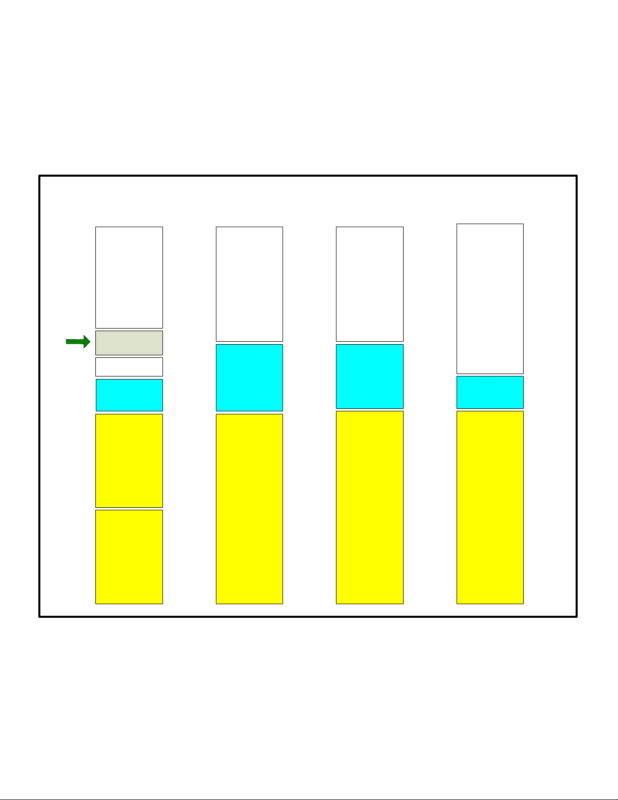
DS4830A User’s Guide
2K * 16
SRAM
16K * 16
FLASH
(SEGMENT 0)
4K * 16
UTILITY ROM
PROGRAM
SPACE
16K * 16
FLASH
(SEGMENT 1)
0000h
3FFFh
4000h
7FFFh
8FFFh
A000h
A7FFh
FFFFh
8000h
32K * 8
LOWER HALF
(SEGMENT 0)
OF FLASH
DATA SPACE
(BYTE MODE,
CDA0 = 0)
0000h
FFFFh
8000h
32K * 8
UPPER HALF
(SEGMENT 1)
OF FLASH
0000h
FFFFh
DATA SPACE
(BYTE MODE,
CDA0 = 1)
EXECUTING FROM
32K * 16
FLASH
0000h
FFFFh
DATA SPACE
(WORD MODE)
8K * 8
UTILITY ROM
8K * 8
UTILITY ROM
4K * 16
UTILITY ROM
7FFFh
8000h
7FFFh
8000h
7FFFh
8FFFh
9FFFh 9FFFh
2.4.4.3 – Memory Map When Executing from SRAM
When executing from the SRAM:
• The utility ROM can be read as data, starting at 8000h of the data space. The utility ROM cannot be written.
• Reading of flash memory is executed normally. Writing to flash memory requires the use of the utility ROM
routines.
• One page (byte access mode) or both pages (word access mode) of the flash memory can be accessed as data
with an offset of 0000h. For byte access mode, the page of flash accessed is determined by the CDA0 bi t.
Figure 2-5 illustrates the mapping of the flash and utility ROM memory segments into data memory space when code is
executing from the SRAM memory segment.
Figure 2-5: Memory Map When Executing from SRAM
21
Page 22

DS4830A User’s Guide
2.5 – Data Alignment
To support merged program and data memory operation while maintaining efficient memory space usage, the data
memory must be able to support both byte and word mode accessing. Data is aligned in data memory as words, but the
effective data address is resolved to bytes. This data alignment allows program instruction fetching in words while
maintaining data accessibility at the byte level. It is important to realize that this accessibility requires strict word
alignment. All executable or data words must align to an even address in byte mode. Care must be taken when updating
a code segment as misalignment of words will likely result in loss of program execution contr ol .
Memory will always be read as a complete word, whether for program fetch or data access. The program decoder always
uses a full 16-bit word. The data access can utilize a word or an individual byte. Data memory is organized as two bytewide memory banks with common word address decode but two 8-bit data buses. In byte mode, data pointer hardware
reads out the full word containing the selected byte using the effective data word address pointer (the least significant bit
of the byte data pointer is not initially used). Then, the least significant data pointer bit functions as the byte select that is
used to place the correct byte on the data bus. For write access, data pointer hardware addresses a particular word using
the effective data word address while the least significant bit selects the corresponding data bank for write. The contents
of the other byte are left unaffected.
2.6 – Reset Conditions
The DS4830A has several possible sources of reset.
• Power-On/Brownout Reset
• Watchdog Timer Reset
• External Reset
• Internal System Reset
• Soft Reset
Once a reset condition has completed or been removed, code execution begins at the beginning of utility ROM, which is
address 8000h. The utility ROM code interrogates the I2C_SPE, JTAG_SPE, and PWL bits to determine if bootloading is
necessary. If bootloading is not required, execution will jump to the user code reset vector, which is at flash memory
address 0000h.
The RST pin is an input only.
2.6.1 – Power-On/Brownout Reset
The DS4830A provides a power-on reset (POR) circuit to ensure proper initialization of internal device states and analog
circuits. The POR voltage threshold range is between approximately 1.1V and 1.7V. When V
the state of all the DS4830A pins (except DAC port pins), including RST, is weak pullup. The port pins having DAC
function are high impedance on POR.
The DS4830A also includes brownout detection capability. This is an on-chip precision reference and comparator that
monitors the supply voltage, V
, to ensure that it is within acceptable limits. If VDD is below the brownout level (VBO), the
DD
power monitor generates a reset. This can occur when:
• The DS4830A is being powered up and V
• V
drops from an acceptable level to less than VBO.
DD
is above the POR level but still less than VBO.
DD
Once V
exceeds VBO, the DS4830A exits the reset condition and the internal oscillator starts up. After approximately
DD
1ms the DS4830A performs the following task s.
• All registers and circuits enter their reset state
• The POR flag in the Watchdog Control Register i s se t to indicate the source of the reset
• The DS4830A begins normal operation (CPU State)
• Code execution begins at utility ROM location 8000h
The transition between POR, Brownout, and normal operation is detailed in Figure 2-6: DS4830A State Diagram.
Note: If V
is below VBO, there is a chance that the SRAM gets corrupted. If the POR flag in WDCN is set, all data in
DD
SRAM should be re-initialized.
is below the POR level,
DD
22
Page 23
BROWNOUT STATE
CPU DISABLED
ANALOG ACTIVE
SYSTEM CLOCK
STARTUP DELAY
CPU MODE
DIGITAL CORE ON
ANALOG ON
CODE EXECUTION
VDD > V
BO
VDD < VBO
POR
VDD < VBO
DS4830A User’s Guide
Figure 2-6: DS4830A State Diagram
2.6.2 – Watchdog Timer Reset
The watchdog timer is a programmable hardware timer that can be used to reset the processor in case a software lockup
or other unrecoverable error occurs. Once the watchdog is enabled, software must reset the watchdog timer periodically.
If the processor does not reset the watchdog tim er before it elapses, the watchdog can initiate a reset.
If the watchdog resets the processor, the DS4830A will remain in reset for 12 clock cycles. When a reset occurs due to a
watchdog timeout, the Watchdog Timer Reset Flag (WTRF) in the WDCN register is set to indicate the source of the
reset.
2.6.3 – External Reset
During normal operation, the DS4830A is placed into external reset when the RST pin is held at logic 0 for at least four
clock cycles. Once the DS4830A enters reset mode, it remains in reset as long as the RST pin is held at logic 0. After the
RST pin returns to logic 1, the processor exits reset wi thin 12 clock cycles.
An external reset pulse on the RST pin will reset the DS4830A and return to normal CPU mode operation within 10 clock
cycles.
23
Page 24

DS4830A User’s Guide
2.6.4 – Internal System Resets
There are two possible sources of internal system resets. An internal reset will hold the DS4830A in reset mode for 12
clock cycles.
1. When data BBh is written to the special I
2. When in-system programming is complete and the ROD bit is set to 1.
2.6.5 – Software Reset
The device UROM provides option to soft reset through the application program. The application program jumps to UROM
code which generates the internal system reset. UROM location 8854h has code when executed generates internal reset.
Application program can jump to this location to generate software reset.
asm (“LJUMP #8854h”)
2
C slave address 34h.
2.7 – Clock Generation
The DS4830A generates its 20MHz peripheral clock using an internal oscillator and generates 10MHz instruction clock
using divide by 2 circuit. This oscillator starts up when V
approximately 1ms in the oscillator start up and beginning of clock. This delay ensures that the clock is stable prior to
beginning normal operation.
exceeds the brownout voltage level, VBO. There is a delay of
DD
24
Page 25

DS4830A User’s Guide
REGISTER MODULE
AP (08h)
A (09h)
PFX (0Bh)
IP (0Ch)
SP (0Dh)
DPC (0Eh)
DP (0Fh)
00h
AP
A[0]
PFX[0]
IP 01h
APC
A[1]
PFX[1]
SP
02h
A[2]
PFX[2]
IV
03h
A[3]
PFX[3]
OFFS
DP[0]
04h
PSF
A[4]
PFX[4]
DPC
07h
A[7]
PFX[7]
LC[1]
BP
DP[1]
08h
SC
A[8] GRS
09h
A[9] GRH
0Ah
A[10] GRXL
0Eh
A[14] 0Fh
WDCN
A[15]
SECTION 3 – SYSTEM REGISTER DESCRIPTIONS
Most functions of the DS4830A are controlled by sets of registers. These registers provide a working space for memory
operations as well as configuring and addressing peripheral registers on the device. Registers are divided into two major
types: system registers and peripheral registers. The common register set, also known as the system registers, includes
ALU access and control registers, accumulator registers, data pointers, interrupt vectors and control, and stack pointer.
The peripheral registers define addition al functionality and the functionality is broken up into di screte modules.
This section describes the DS4830A’s system registers. Table 3-1 shows the DS4830A system register map. Table 3-2
explains system register bit functions. This is followed by a detailed bit description.
Table 3-1: System Register Map
REGISTER
INDEX
05h IC A[5] PFX[5] GR
06h IMR A[6] PFX[6] LC[0] GRL
0Bh IIR A[11] FP
0Ch A[12]
0Dh A[13]
25
Page 26
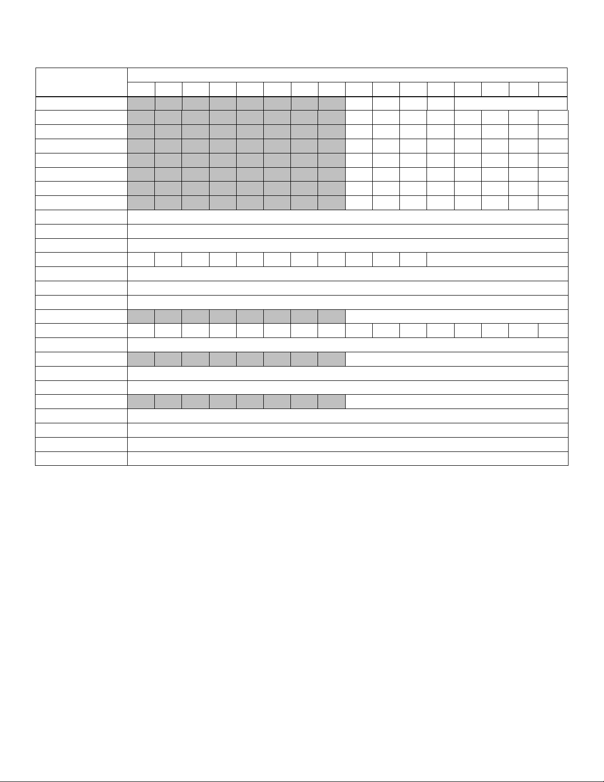
REGISTER BIT NUMBER
15
14
13
12
11
10 9 8 7 6 5 4 3 2 1 0
AP
— — — — AP (4 bits)
IC
— — — — — — INS
IGE
A[n] (n=15:0)
A[n] (16 bits)
LC[0]
LC[0] (16 bits)
WBS2
WBS1
SDPS1
SDPS0
GRL
GRL (8 bits)
FP
FP = BP[OFFS] (16 bits)
Table 3-2. System Register Bit Functions
REGISTER
APC CLR IDS — — — MOD2 MOD1 MOD0
PSF Z S — GPF1 GPF0 OV C E
IMR IMS — IM5 IM4 IM3 IM2 IM1 IM0
SC TAP — — CDA0 — ROD PWL —
IIR IIS — II5 II4 II3 II2 II1 II0
WDCN POR EWDI WD1 WD0 WDIF WTRF EWT RWT
PFX[n] (n=7:0) PFX[n] (16 bits)
IP IP (16 bits)
SP — — — — — — — — — — — SP (5 bits)
IV IV (16 bits)
LC[1] LC[1] (16 bits)
OFFS OF F S (8 bits)
DPC — — — — — — — — — — —
GR GR (16 bits)
DS4830A User’s Guide
WBS0
BP BP (16 bits)
GRS GRS (16 bits) = (GRL : GRH)
GRH GRH (8 bits)
GRXL GRXL (16 bits) = (GRL.7, 8 bits) : (GR L, 8 bits)
DP[0] DP[0] (16 bits)
DP[1] DP[1] (16 bits)
26
Page 27

Bit
Name
Function
7:4
Reserved
Reserved. All reads return 0.
Active Accumulator Select. These bits select which of the 16 accumulator registers are used for
arithmetic and logical operations. If the APC register has been set to perform automatic
n. If a ‘MOVE AP, Acc’ instruction is executed, any enabled AP
inc/dec/modulo control will take precedence over the transfer of Acc data into AP.
Bit
Name
Function
AP Clear. Writing this bit to 1 clears the accumulator pointer AP to 0. Once set, this bit will
reads from this bit return 0.
Increment/Decrement Select. If this bit is set to 0, the accumulator pointer AP is incremented following
each arithmetic or logical operation according to MOD[2:0]. If this bit is set to 1, the accumulator
pointer AP is decremented following each arithmetic or logical operation according to MOD[2:0]. If
MOD[2:0] is set to 000, the setting of this bit is ignored.
5:3
Reserved
Reserved. All reads return 0.
Accumulator Pointer Auto Increment/Decrement Modulus. If these bits are set to a nonzero value, the
nted or decremented following each
MOD[2:0]
AUTO INCREMENT/DECREMENT MODE
000
No auto-increment/decrement (default)
001
Increment/decrement AP[0] modulo 2
010
Increment/decrement AP[1:0] modulo 4
011
Increment/decrement AP[2:0] modulo 8
100
Increment/decrement AP modulo 16
101 to 111
Reserved (modulo 16 when set)
Bit
Name
Function
Zero Flag. The value of this bit flag equals 1 whenever the active accumulator is equal to zero. This
bit equals 0 if the active accumulator is not equal to 0.
6 S Sign Flag. This bit flag mirrors the current value of the high bit of the active accumulator (Acc.15).
5
Reserved
Reserved. All reads return 0.
4:3
GPF[1:0]
General-Purpose Flags. These general-purpose flag bits are provided for user software cont rol.
Overflow Flag. This flag is set to 1 if there is a carry out of bit 14 but not out of bit 15, or a carry out of
out of bit 14 from the last arithmetic operation, otherwise, the OV flag remains as 0. OV
from two negative operands.
Carry Flag. This bit flag is set to 1 whenever an add or subtract operation (ADD, ADDC, SUB, SUBB)
. Reference the
instruction set documentation for details.
Equals Flag. This bit flag is set to 1 whenever a compare operation (CMP) returns an equal result. If a
CMP operation returns not equal, this bit i s cleared.
3.1 – Accumulator Pointer Register (AP, 08h[00h])
Initialization: This register is cleared t o 00h on al l forms of reset.
Access: Unrestricte d d irect read/write ac cess.
DS4830A User’s Guide
3:0 AP[3:0]
increment/decrement of the active accumulator, this setting will be automatically changed after each
arithmetic or logical operatio
3.2 – Accumulator Pointer Control Register (APC, 08h[01h])
Initialization: This register is cleared to 00h on all forms of reset.
Access: Unrestricte d d irect read/write ac cess.
7 CLR
6 IDS
2:0 MOD[2:0]
automatically be reset to 0 by hardware. If a ‘MOVE APC, Acc’ instruction is executed requesting that
AP be set to 0 (i.e., CLR = 1), the AP clear function overrides any enabled inc/dec/modulo control. All
accumulator pointer (AP[3:0]) will be automatically increme
arithmetic or logical operation. The mode for the auto-increment/ decrement is determined a s follows:
3.3 – Processor Status Flags Register (PSF, 08h[04h])
Initialization: This register is cleared to 80h on all forms of reset.
Access: Bit 7 (Z), bit 6 (S), and bit 2 (OV) are read only. Bits [4:3] (GPF[1:0]), bit 1 (C), and bit 0 (E) are unrestricted
read/write.
7 Z
2 OV
1 C
0 E
bit 15 but not
indicates a negative number resulted as the sum of two positive operands, or a positive sum resulted
returns a carry or borrow. This bit flag is cleared to 0 whenever an add or subtract operation does not
return a carry or borrow. Many other instructions potentially affect the carry bit
27
Page 28
Bit
Name
Function
7:2
Reserved
Reserved. All reads return 0.
Interrupt In Service. The INS is set by hardware automatically when an interrupt is acknowledged. No
or POPI instruction.
Interrupt Global Enable. If this bit is set to 1, interrupts are globally enabled, but still must be locally
enabled to occur. If this bit is set to 0, all interr upts are disabled.
Bit
Name
Function
7
IMS
Interrupt Mask for System Modules
6
Reserved
Reserved. All reads return 0.
5
IM5
Interrupt Mask for Register Module 5
4
IM4
Interrupt Mask for Register Module 4
3
IM3
Interrupt Mask for Register Module 3
2
IM2
Interrupt Mask for Register Module 2
1
IM1
Interrupt Mask for Register Module 1
0
IM0
Interrupt Mask for Register Module 0
Bit
Name
Function
Test Access Port (JTAG) Enable. This bit controls whether the Test Access Port special-function pi ns
function pins.
6:5
Reserved
Reserved. All reads return 0.
Code Data Access Bit 0.
The CDA0 bit is used to logically map the flash memory pages to the data space for read/write access.
CDA0
Byte Mode Active Page
Word Mode Active Page
0
P0
P0 and P1
1
P1
P0 and P1
3
Reserved
Reserved. All reads return 0.
ROM Operation Done. This bit is used to signify completion of a ROM operation sequence to the
once the control unit acknowledges the done indi cat ion.
Password Lock. This bit defaults to 1 on a power-on reset. When this bit is 1, it requires a 32-byte
the password protection for these ROM routines.
0
Reserved
Reserved. All reads return 0.
3.4 – Interrupt and Control Register (IC, 08h[05h])
Initialization: This register is cleared to 00h on all forms of reset.
Access: Unrestricte d d irect read/write ac cess.
DS4830A User’s Guide
1 INS
0 IGE
further interrupts occur as long as the INS remains set. The interrupt service routine can clear the INS
bit to allow interrupt nesting. Otherwise, the INS bit is cleared by hardware upon execution of an RETI
3.5 – Interrupt Mask Register (IMR, 08h[06h])
Initialization: This register is cleared to 00h on all forms of reset.
Access: Unrestricte d r ead/write access.
The first six bits in this register are interrupt mask bits for modules 0 to 5, one bit per module. The eighth bit, IMS, serves
as a mask for any system module interrupt sources. Setting a mask bit allows the enabled interrupt sources for the
associated module or system (for the case of IMS) to generate interrupt requests. Clearing the mask bit effectively
disables all interrupt sources associated with that specific module or all system interrupt sources (for the case of IMS).
The interrupt mask register is intended to facilitate user-definable interrupt prioritization.
3.6 – System Control Register (SC, 08h[08h])
Initialization: This register is reset to 100 0 00s0b on all reset. Bit 1 (PWL) is set to 1 on a power-on reset o nly.
Access: Unrestricted read/write access.
7 TAP
4 CDA0
2 ROD
1 PWL
are enabled. The TAP defaults to being enabled. Clearing this bit to 0 disables the TAP special
The logical data memory addresses of the flash depend on whether execution is from Utility ROM or
SRAM. The CDA0 bit is not needed if data memory i s accessed in word mode.
control units. This allows the Debug engine to determine the status of a ROM sequence. Setti ng this
bit to logic 1 causes an internal system reset if the JTAG SPE bit is also set. Setting the ROD bit will
clear the JTAG SPE and I2C_SPE bits if set. The ROD bit will be automatically cleared by hardware
password to be matched with the password in the program space before allowing access to the
password protected in-circuit debug or bootst rap loader ROM routines. Clearing this bit to 0 di sables
28
Page 29

DS4830A User’s Guide
Bit
Name
Function
7
IIS
Interrupt Identifier Flag for System Modules
6
Reserved
Reserved. All reads return 0.
5
II5
Interrupt Identifier Flag for Register Module 5
4
II4
Interrupt Identifier Flag for Register Module 4
3
II3
Interrupt Identifier Flag for Register Module 3
2
II2
Interrupt Identifier Flag for Register Module 2
1
II1
Interrupt Identifier Flag for Register Module 1
0
II0
Interrupt Identifier Flag for Register Module 0
BIT
DESCRIPTION
These registers (n=0 to 15) act as the accumulat or for all ALU arithmetic and logical operation s
working register.
BIT
NAME
DESCRIPTION
The Prefix register provides a means of supplying an additional 8 bits of high-order data for use by
the succeeding instruction as well as providing additional indexing capabilities. This register will
order bits for the register source and destination specified in the following
n of registers 0h to 7h for
WRITE
TO
SOURCE REGISTER
RANGE
DESTINATION
REGISTER RANGE
PFX[0]
0h to Fh
0h to 7h
PFX[1]
10h to 1Fh
0h to 7h
PFX[2]
0h to Fh
8h to Fh
PFX[3]
10h to 1Fh
8h to Fh
PFX[4]
0h to Fh
10h to 17h
PFX[5]
10h to 1Fh
10h to 17h
PFX[6]
0h to Fh
18h to 1Fh
PFX[7]
10h to 1Fh
18h to 1Fh
3.7 – Interrupt Identification Register (IIR, 08h[0Bh])
Initialization: This register is cleared to 00h on all forms of reset.
Access: Read only.
The first six bits in this register indicate interrupts pending in modules 0 to 5, one bit per module. The eighth bit, IIS,
indicates a pending system interrupt, such as from the watchdog timer. The interrupt pending flags will be set only for
enabled interrupt sources waiting for service. The interrupt pending flag will be cleared when the pending interrupt
sources within that module are disabled or when the interrupt flags are cleared by software
3.8 – Watchdog Control Register (WDCN, 08h[0Fh])
Initialization: Bits 5, 4, 3 and 0 are cleared to 0 on all forms of reset; for others, see individual bit descriptions.
Access: Unrestricte d d irect read/write ac cess.
See the watchdog section for WDCN register description and further detail.
3.9 – Accumulator n Register (A[n], 09h[nh])
Initialization: These registers are cleared to 0000h on all forms of reset.
Access: Unrestricte d d irect read/write ac cess.
A[n][15:0]
when selected by the accumulator pointer (AP ). T hey can also be used as a general-purpose
3.10 – Prefix Register (PFX[n], 0Bh[n])
Initialization: This register is cleared to 0000h on all forms of reset.
yAccess: Unrestricted direct read/write access.
only hold any data written to it for one execution cycle, after which it will revert to 0000h. Although
this is a 16-bit register, only the lower 8 bits are actually used for prefixing purposes by the next
instruction. Writing to or reading from any index in the Prefix module will select the same 16-bit
15:0 PFX[n][15:0]
register. However, when the Prefix register is written, the index n used for the PFX[n] write also
determines the highinstruction.
The index selection reverts to 0 (default mode allowing selectio
destinations) after one cycle in the same manner as the contents of the Prefix register.
29
Page 30

BIT
DESCRIPTION
This register contains the address of the next i nst ruction to be executed and is automatically
program flow to jump to that address. Reading from this register will not affect program flow.
BIT
DESCRIPTION
15:4
Reserved; all reads return 0.
These four bits indicate the current top of the hardware stack, from 0h to 1Fh. This pointer is
the stack.
BIT
DESCRIPTION
This register contains the address of the interrupt service routine. The interrupt handler will
generate a CALL to this address whenever an interrupt is acknowledged.
BIT
DESCRIPTION
This register is used as the loop counter for t he DJNZ LC[0], src operation. This operation
= 0.
BIT
DESCRIPTION
This register is used as the loop counter for t he DJNZ LC[1], src operation. This operation
= 0.
BIT
DESCRIPTION
This 8-bit register provides the Frame Pointer (FP) offset from the base pointer (BP). The Frame
is formed by unsigned addition of Frame Pointer Base Register (BP) and Frame Pointer
decremented when using the Frame Pointer for write operations. A carry out or borrow resulting
from an increment/decrement operation has no effect on the Frame Pointer Base Register (BP).
3.11 – Instruction Pointer Register (IP, 0Ch[00h])
Initialization: This register is cleared to 8000h on all forms of reset.
Access: Unrestricte d d irect read/write ac cess.
DS4830A User’s Guide
15:0
incremented by 1 after each program fetch. Writing an address value to this register will caus e
3.12 – Stack Pointer Register (SP, 0Dh[01h])
Initialization: This register is cleared to 001Fh on al l forms of reset.
Access: Unrestricte d d irect read/write ac cess.
4:0
incremented after a value is pushed on the stack and decremented before a value is popped from
3.13 – Interrupt Vector Register (IV, 0Dh[02h])
Initialization: This register is cleared to 0000h on all forms of reset.
Access: Unrestricted direct read/write access.
15:0
3.14 – Loop Counter 0 Register (LC[0], 0Dh[06h])
Initialization: This register is cleared to 0000h on all forms of reset.
Access: Unrestricte d d irect read/write ac cess.
15:0
decrements LC[0] by one and then jumps to the address specified in the instruction by src if LC[0]
3.15 – Loop Counter 1 Register (LC[1], 0Dh[07h])
Initialization: This register is cleared to 0000h on all forms of reset.
Access: Unrestricte d d irect read/write ac cess.
15:0
decrements LC[1] by one and then jumps to the address specified in the instruction by src if LC[1]
3.16 – Frame Pointer Offset Register (OFFS, 0Eh[03h])
Initialization: This register is cleared to 00h on all forms of reset.
Access: Unrestricte d d irect read/write ac cess.
Pointer
7:0
Offset Register (Offs). The contents of this register can be post-incremented or post-decremented
when using the Frame Pointer for read operations and may be pre-incremented or pre-
30
Page 31

BIT
NAME
DESCRIPTION
15:5
RESERVED
Reserved. All reads return 0.
Word/Byte Select 2. This bit selects access mode for BP[OFFS]. When WBS2 is set to logic 1, the
BP[Offs] is operated in word mode for data memory access; when WBS2 is cleared to logic 0,
BP[Offs] is operated in byte mode for data memory access.
Word/Byte Select 1. This bit selects access mode for DP[1]. When WBS1 is set to logic 1, the
is operated in byte mode for data memory acces s.
Word/Byte Select 0. This bit selects access mode for DP[0]. When WBS0 is set to logic 1, the
is operated in byte mode for data memory acces s.
Source Data Pointer Select Bits[1:0]. These bits select one of the three data pointers as the active
source pointer for the load operation. A new data pointer must be selected before being used to
SDPS1
SDPS0
SOURCE POINTER SELECTION
0
0
DP[0]
0
1
DP[1]
1
0
FP (BP[Offs])
1 1 Reserved (select FP if set)
are explicitly cleared to 00b or the DP[0] register is written by an instruction. Also, modifying the
of the SDPS bits to reflect the active source pointer selection.
BIT
DESCRIPTION
This register is intended primarily for supporting byte operations on 16-bit data. The 16-bit register
swappable through the GRS 16-bit register.
BIT
DESCRIPTION
This register reflects the low byte of the GR register and is intended primarily for supporting byte
the GR register.
BIT
DESCRIPTION
This register serves as the base pointer for the Frame Pointer (FP). The Frame Pointer is formed
Pointer Base Register (BP) and Frame Pointer Offset Register
performed on the offset (OFFS) register.
3.17 – Data Pointer Control Register (DPC, 0Eh[04h])
Initialization: This register is cleared to 001Ch on all forms of reset.
Access: Unrestricte d d irect read/write ac cess.
4 WBS2
DS4830A User’s Guide
3 WBS1
2 WBS0
1:0 SDPS[1:0]
DP[1] is operated in word mode for data memory access; when WBS1 is cleared to logic 0, DP[1]
DP[0] is operated in word mode for data memory access; when WBS0 is cleared to logic 0, DP[0]
read data memory:
These bits default to 00b but do not activate DP[0] as an active source pointer until the SDPS bits
register contents of a data/frame pointer register (DP[0], DP[1], BP or Offs) will change the setting
3.18 – General Register (GR, 0Eh[05h])
Initialization: This register is cleared to 0000h on all forms of reset.
Access: Unrestricte d d irect read/write access.
15:0
is byte-readable, byte-writeable through the corresponding GRL and GRH 8-bit registers and byte-
3.19 – General Register Low Byte (GRL, 0Eh[06h])
Initialization: This register is cleared to 00h on all forms of reset.
Access: Unrestricte d d irect read/write ac cess.
7:0
operations on 16-bit data. Any data written to the GRL register will also be stored in the low byte of
3.20 – Frame Pointer Base Register (BP, 0Eh[07h])
Initialization: This register is cleared to 0000h on all forms of res et.
Access: Unrestricte d d irect read/write ac cess.
15:0
by unsigned addition of Frame
(Offs). The content of this base pointer register is not affected by increment/decrement operations
31
Page 32

BIT
DESCRIPTION
This register is intended primarily for supporting byte operations on 16-bit data. This 16-bit read
only register returns the byte-swapped value for the data contained in the GR register.
BIT
DESCRIPTION
This register reflects the high byte of the GR register and is intended primarily for supporting byte
of the GR register.
BIT
DESCRIPTION
15:0
This register provides the sign extended low by te of GR as a 16-bit source.
BIT
DESCRIPTION
15:0
This register provides the current value of the frame pointer (BP[Offs]).
BIT
DESCRIPTION
This register is used as a pointer to access data memory. DP[0] can be automatically incremented
or decremented following each read operation or can be automatically incremented or
decremented before each write operation.
BIT
DESCRIPTION
This register is used as a pointer to access data m emory. DP[1] can be automatically incremented
decremented before each write operation.
3.21 – General Register Byte-Swapped (GRS, 0Eh[08h])
Initialization: This register is cleared to 0000h on all forms of reset
Access: Unrestricte d r ead-only access.
15:0
3.22 – General Register High Byte (GRH, 0Eh[09h])
Initialization: This register is cleared to 00h on all forms of reset.
Access: Unrestricte d d irect read/write ac cess.
DS4830A User’s Guide
7:0
operations on 16-bit data. Any data written to the GRH register will also be stored in the high byte
3.23 – General Register Sign Extended Low Byte (GRXL, 0Eh[0Ah])
Initialization: This register is cleared to 0000h on all forms of reset.
Access: Unrestricted direct read-only access.
3.24 – Frame Pointer Register (FP, 0Eh[0Bh])
Initialization: This register is cleared to 0000h on all forms of reset.
Access: Unrestricted direct read-only access.
3.25 – Data Pointer 0 Register (DP[0], 0Fh[03h])
Initialization: This register is cleared to 0000h on all forms of reset.
Access: Unrestricte d d irect read/write ac cess.
15:0
3.26 – Data Pointer 1 Register (DP[1], 0Fh[07h])
Initialization: This register is cleared to 0000h on all forms of reset.
Access: Unrestricte d d irect read/write ac cess.
15:0
or decremented following each read operation or can be automatically incremented or
32
Page 33

Reg
M0
M1
M2
M3
M4
M5
0
PO2
I2CBUF_M
I2CBUF_S
MCNT
ADCN
QTDATA
1
PO1
I2CST_M
I2CST_S
MA
SENR
QTCN
2
PO0
I2CIE_M
MPNTR
MB
ADST
LTIL
3
EIF2
PO6
I2CTXFST
MC2
ADST1
HTIL
4
EIF1
CRC8IN
I2CTXFIE
MC1
ADDATA
SPIB_M
5
EIF0
MIIR1
I2CRXFST
MC0
SPIB_S
PWMDATA
6
GTV1
EIF6
I2CRXFIE
GTCN2
DADDR
PWMCN
7
GTCN1
EIE6
I2CST2_S
SHFT
MIIR4
PWMSYNC
8
PI2
PI6
RPNTR
MC1R
TEMPCN
LTIH
9
PI1
SVM
I2CCN_S
MC0R
SHCN
HTIH
10
PI0
GTC2
QTLST
11
GTC1
GTV2
PINSEL
12 I2CCN_M
I2CSLA_S
GP_REG1
REFAVG
13
EIE2
I2CCK_M
I2CSLA2_S
GP_REG2
14
EIE1
I2CTO_M
I2CSLA3_S
MACSEL
TWR
MIIR5
15
EIE0
I2CSLA_M
I2CSLA4_S
USER_INT
RPCFG
16
PD2
EIES6
I2CIE2_S
GP_REG3
SPICN_S
17
PD1
PD6
MADDR
GP_REG4
SPICF_S
18
PD0
MADDR2
GP_REG5
SPICK_S
SPICN_M
19
EIES2
MADDR3
GP_REG6
I2C_SPB
SPICF_M
20
EIES1
MADDR4
GP_REG7
DEV_NUM
SPICK_M
21
EIES0
CRC8OUT
CUR_SLA
GP_REG8
DACD0
22
I2CIE_S
GP_REG9
DACD1
23 ADCG1
GP_REG10
DACD2
24 ADCG2
ICDT0
GP_REG11
DACD3
25 ADVOFF
ICDT1
GP_REG12
DACD4
26
ICDC
GP_REG13
DACD5
27 ADCG3
ICDF
GP_REG14
DACD6
28 ADCG4
ICDB
GP_REG15
DACD7
29 CHIPREV
ICDA
GP_REG16
DACCFG
30
I2CSLA2_M
ICDD
ADADDR
31
SECTION 4 – PERIPHERAL REGISTER DESCRIPTIONS
DS4830A User’s Guide
The DS4830A has sixteen 16-bit general-purpose registers GP_REG1-16 for application usage.
33
Page 34

DS4830A User’s Guide
MODULE 0
Register
index
15
14
13
12
11
10 9 8 7 6 5 4 3 2 1 0
4.1 – Module 0 Peripheral Registers
PO2 00h PO2[7:0]
PO1 01h PO1[7:0]
PO0 02h PO0[7:0]
EIF2 03h IFP2[7:0]
EIF1 04h IFP1[7:0]
EIF0 05h IFP0[7:0]
GTV1 06h GTV1[15:0]
GTCN1 07h - - - GTR MODE CLK_SEL[1:0] GTIE - - - GTIF - GTPS[2:0]
PI2 08h PI2[7:0]
PI1 09h PI1[7:0]
PI0 0Ah PI0[7:0]
GTC1 0Bh GTC1[15:0]
EIE2 0Dh IEP2[7:0]
EIE1 0Eh IEP1[7:0]
EIE0 0Fh IEP0[7:0]
PD2 10h PD2[7:0]
PD1 11h PD1[7:0]
PD0 12h PD0[7:0]
EIES2 13h IESP2[7:0]
EIES1 14h IESP1[7:0]
EIES0 15h IESP0[7:0]
34
Page 35

DS4830A User’s Guide
MODULE 1
Register
index
15
14
13
12
11
10 9 8 7 6 5 4 3 2 1 0
4.2 – Module 1 Peripheral Registers
I2CBUF_M 00h D[15:0]
I2CST_M 01h I2CBUS I2CBUSY - I2CAMI2 I2CSPI I2CSCL I2CROI I2CGCI I2CNACKI - I2CAMI I2CTOI I2CSTRI I2CRXI I2CTXI I2CSRI
I2CIE_M 02h - - - - I2CSPIE I2CAMI2E I2CROIE I2CGCIE I2CNACKIE - I2CAMIE I2CTOIE I2CSTRIE I2CRXIE I2CTXIE I2CSRIE
PO6 03h - PO6[6:0]
CRC8IN 04h CRC8IN[7:0]
MIIR1 05h - - - - - - - I2CM SVM P6_6 P6_5 P6_4 P6_3 P6_2 P6_1 P6_0
EIF6 06h - IFP6[6:0]
EIE6 07h - IEP6[6:0]
PI6 08h - PI6[6:0]
SVM 09h - - - - SVMTH[3:0] - - - - SVMI SVMIE SVMRDY SVMEN
I2CCN_M 0Ch - - - I2CM_ALT ADD2EN SMB_MOD I2CSTREN I2CGCEN I2CSTOP I2CSTART I2CACK I2CSTRS - - I2CMST I2CEN
I2CCK_M 0Dh I2CCKH[7:0] I2CCKL[7:0]
I2CTO_M 0Eh I2CTO[7:0]
I2CSLA_M 0Fh SLAVE_ADDRESS[7:1] I2CMODE
EIES6 10h - IESP6[6:0]
PD6 11h - PD6[6:0]
CRC8OUT 15h - CRC8OUT[7:0]
ADCG1 17h ADC VOLTAGE SCALE TRIM FOR GAIN1[13:0] - ADCG2 18h ADC VOLTAGE SCALE TRIM FOR GAIN2[13:0] - -
ADVOFF 19h ADC VOLTAGE OFFSET [15:0]
ADCG3 1Bh ADC VOLTAGE SCALE TRIM FOR GAIN3[13:0] - ADCG4 1Ch ADC VOLTAGE SCALE TRIM FOR GAIN4[13:0] - -
CHIPREV 1Dh CHIPREV[15:0]
I2CSLA2_M 1Eh SLAVE_ADDRESS[7:1] I2CMODE
35
Page 36

MODULE 2
Register
index
15
14
13
12
11
10 9 8 7 6 5 4 3 2 1 0
4.3 – Module 2 Peripheral Registers
DS4830A User’s Guide
I2CBUF_S 00h
I2CST_S 01h I2CBUS I2CBUSY - - - I2CSCL I2CROI I2CGCI I2CNACKI - I2CAMI I2CTOI I2CSTRI I2CRXI I2CTXI I2CSRI
MPNTR 02h - - - - - PAGE[2:0] MEM_PNTR[7:0]
I2CTXFST 03h - - - - - - THSH I2CTXFIE 04h TXPG_EN - - - - - THSH -
I2CRXFST 05h - - - - FULL - THSH EMPTY
I2CRXFIE 06h RXFIFO_EN - - - FULL - THSH EMPTY
I2CST2_S 07h - - I2CSPI SADI MADI - I2CXFRON -
RPNTR 08h - - - - - PAGE[2:0] MEM_PNTR[7:0]
I2CCN_S 09h - - ADDR4EN ADDR3EN ADDR2EN SMB_MOD I2CSTREN I2CGCEN I2CSTOP I2CSTART I2CACK I2CSTRS - I2CMODE - I2CEN
I2CSLA_S 0Ch SLAVE_ADDRESS[7:1] I2CMODE
I2CSLA2_S 0Dh SLAVE_ADDRESS[7:1] I2CMODE
I2CSLA3_S 0Eh SLAVE_ADDRESS[7:1] I2CMODE
I2CSLA4_S 0Fh SLAVE_ADDRESS[7:1] I2CMODE
I2CIE2_S 10h - - I2CSPIE SADIE MADIE - - -
MADDR 11h - - - ROLLOVR - PAGE[2:0] MEM_ADDR[7:0]
MADDR2 12h - - - ROLLOVR - PAGE[2:0] MEM_ADDR[7:0]
MADDR3 13h - - - ROLLOVR - PAGE[2:0] MEM_ADDR[7:0]
MADDR4 14h - - - ROLLOVR - PAGE[2:0] MEM_ADDR[7:0]
CURR_SLA 15h MADR_EN4 MADR_EN3 MADR_EN2 MADR_EN1 SLA4 SLA3 SLA2 SLA1
I2CIE_S 16h - - - - - - I2CROIE I2CGCIE I2CNACKIE - I2CAMIE I2CTOIE I2CSTRIE I2CRXIE I2CTXIE I2CSRIE
ICDT0 18h ICDT0[15:0]
ICDT1 19h ICDT1[15:0]
ICDC 1Ah DME - REGE - CMD[3:0]
ICDF 1Bh - - - - PSS1 PSS0 JTAG_SPE TXC
ICDB 1Ch ICDB[7:0]
ICDA 1Dh ICDA[15:0]
ICDD 1Eh ICDD[15:0]
D[15:0]
36
Page 37

DS4830A User’s Guide
MODULE 3
Register
index
15
14
13
12
11
10 9 8 7 6 5 4 3 2 1 0
4.4 – Module 3 Peripheral Registers
MCNT 00h OF MCW CLD SQU OPCS MSUB MMAC SUS
MA 01h MA[15:0]
MB 02h MB[15:0]
MC2 03h MC2[15:0]
MC1 04h MC1[15:0]
MC0 05h MC0[15:0]
GTCN2 06h - - - GTR MODE CLK_SEL[1:0] GTIE - - - GTIF - GTPS[2:0]
SHFT 07h SHC - - - - - SR SL
MC1R 08h MC1R[15:0]
MC0R 09h MC0R[15:0]
GTC2 0Ah GTC2[15:0]
GTV2 0Bh GTV2[15:0]
GP_REG1 0Ch GP_REG1[15:0]
GP_REG2 0Dh GP_REG2[15:0]
MACSEL 0Eh - - - - - - - MACRSEL
USER_INT 0Fh SW_F3 SW_F2 SW_F1 SW_F0 SW_INT3 SW_INT2 SW_INT1 SW_INT0
GP_REG3 10h GP_REG3[15:0]
GP_REG4 11h GP_REG4[15:0]
GP_REG5 12h GP_REG5[15:0]
GP_REG6 13h GP_REG6[15:0]
GP_REG7 14h GP_REG7[15:0]
GP_REG8 15h GP_REG8[15:0]
GP_REG9 16h GP_REG9[15:0]
GP_REG10 17h GP_REG10[15:0]
GP_REG11 18h GP_REG11[15:0]
GP_REG12 19h GP_REG12[15:0]
GP_REG13 1Ah GP_REG13[15:0]
GP_REG14 1Bh GP_REG14[15:0]
GP_REG15 1Ch GP_REG15[15:0]
GP_REG16 1Dh GP_REG16[15:0]
37
Page 38

DS4830A User’s Guide
4.5 – Module 4 Peripheral Registers
MODULE 4
Register index 15 14 13 12 11 10 9 8 7 6 5 4 3 2 1 0
ADCN 00h ADCCLK[2:0] NUM_SMP[4:0] ADDAINV ADCONT ADDAIE LOC_OVR ADACQ[3:0]
SENR 01h -
ADST 02h - - - - ENABLE_2X - - - ADCAVG ADCONV ADCFG ADIDX[4:0]
ADST1 03h - - SH1DAI SH0DAI INTDAI ADDAI
ADDATA 04h ADDATA[15:0], SEE ADC SECTION FOR DETAILS
SPIB_S 05h SPIB[15:0]
DADDR 06h ADDR[6:0] RWN DATA[7:0]
MIIR4 07h - - - - - SPI_S TWI ADC
TEMPCN 08h - - - - - INT_IEN - - - - -
SHCN 09h SSC[3:0]
PINSEL 0Bh PINSEL[15:0]
REFAVG 0Ch - - - - - - REFOUT INTAVG - - INTAVG[1:0] SH1AVG[1:0] SH0AVG[1:0]
TWR 0Eh TWEN TWCP[2:0] TWIE TWCSDIS TWI BUSY
RPCFG 0Fh - - - - - - REFB_CFG REFA_CFG
SPICN_S 10h STBY SPIC ROVR WCOL MODF MODFE MSTM SPIEN
SPICF_S 11h ESPII SAS - - - CHR CKPHA CKPOL
SPICK_S 12h SPICK[7:0]
I2C_SPB 13h - - - - - - - I2C_SPE
DEV_NUM 14h
DACD0 15h - - - - DACD0[11:0]
DACD1 16h - - - - DACD1[11:0]
DACD2 17h - - - - DACD2[11:0]
DACD3 18h - - - - DACD3[11:0]
DACD4 19h - - - - DACD4[11:0]
DACD5 1Ah - - - - DACD5[11:0]
DACD6 1Bh - - - - DACD6[11:0]
DACD7 1Ch - - - - DACD7[11:0]
DACCFG 1Dh DACCFG7[1:0] DACCFG6[1:0] DACCFG5[1:0] DACCFG4[1:0] DACCFG3[1:0] DACCFG2[1:0] DACCFG1[1:0] DACCFG0[1:0]
ADADDR 1Eh - - - ADSTART[4:0] - - - ADEND[4:0]
FAST_MODE PIN_DIS1 PIN_DIS0 SH_DUAL - SH1_ALGN SHDAI1_EN SMP_HLD1 CLK_SEL SH0_ALGN SHDAI0_EN SMP_HLD0
BOOT_DIS
- INT_TRIG_EN1
INT_TRIG1
INT_ALIGN
- - INT_TRIG_EN0 INT_TRIG0
- - - INT_TEMP
DEVNUM[6:0]
38
Page 39

DS4830A User’s Guide
MODULE 5
Register
index
15
14
13
12
11
10 9 8 7 6 5 4 3 2 1 0
4.6 – Module 5 Peripheral Registers
QTDATA 00h QTDATA[15:0] SEE QUICK TRIP FOR DETAILS
QTCN 01h - - - QTEN - - - - RW_LST - - LTHT QTIDX[3:0]
LTIL 02h LTIE[7:0] LTIF[7:0]
HTIL 03h HTIE[7:0] HTIF[7:0]
SPIB_M 04h SPIB[15:0]
PWMDATA 05h PWMDATA[15:0] SEE PWM SECTION FOR DETAILS
PWMCN 06h - - - M_EN - - - UPDATE PWM_SEL[3:0] - - REG_SEL[1:0]
PWMSYNC 07h - - - - - - PWMSYNC[9:0]
LTIH 08h LTIE[15:8] LTIF[15:8]
HTIH 09h HTIE[15:8] HTIF[15:8]
QTLIST 0Ah - - - - - - - - QTSTART[3:0] QTSTOP[3:0]
MIIR5 0Eh - - - - - I2C_M QT SPI_M
SPICN_M 12h STBY SPIC ROVR WCOL MODF MODFE MSTM SPIEN
SPICF_M 13h ESPII SAS - - - CHR CKPHA CKPOL
SPICK_M 14h SPICK[7:0]
39
Page 40

System Module
WATCHDOG INTERRUPT
WDCN.WDIF
WDCN.EWDI
(local enable
)
IMR.IMS
Module Enable
Module 0
GPIO INTERRUPTS
External Interrupt Pn.: EIFn.IFPn_m
Local Enable EIEn.IEPn_m
n can be 0,1 or 2 and m can be 0
to 7
TIMER1 INTERRUPT
Timer1
Flag GTIF
Timer Local Enable GTIE
IMR.IM0
Module0 Enable
IIR
.IIS
IIR.II0
Module 3
IMR.IM
3
Module3 Enable
IIR.II3
TIMER2 INTERRUPT
Timer Local Enable GTIE
External Interrupt P
2
.0
: EIF
2
.IFP
2_
0
Local Enable EIE2
.IEP2_0
Timer2
Flag GTIF
Note: Only a few of the DS4830A modules and interrupt sources are shown in this interrupt hierarchy
figure. Please refer to the corresponding sections of this user’s guide for more detailed information
about all of the possible interrupts.
Module 1
External Interrupt P6.
m: EIF
6.IFP6
_m
Local Enable EIE
6.IEP6_m
m can be 0 to 6
PORT6 GPIO INTERRUPTS
Master I
2
C START Interrupt
I2
CST_M
.I2CSRI
Local Enable I
2CIE_
M.I
2CSRIE
Any I2C Interrupt I
2CST_M.x
Local Enable I2CIE
_M.
x
SVM Interrupt SVM
.SVMI
Local Enable SVM.SVMIE
MASTER I
2
C INTERRUPTS
SVM INTERRUPT
Module1 Enable
IIR.
III1
JUMP TO
INTERRUPT
VECTOR
IC.INS
Interrupt is NOT
in Service
IC.IGE
Global Enable
IMR
.IM1
SW Interrupt flag
SECTION 5 – INTERRUPTS
The DS4830A provides a single, programmable interrupt vector (IV) that can be used to handle internal and external
interrupts. Interrupts can be generated from system level sources (e.g., watchdog timer) or by sources associated
with the peripheral modules. Only one interrupt can be handled at a time, and all interrupts naturally have the same
priority. A programmable interrupt mask register allows software-controlled prioritization and nesting of high-priority
interrupts. igure 5-1 shows a diagram of t he i nterrupt hierarchy.
DS4830A User’s Guide
Figure 5-1: Interrupt Hierarchy
40
Page 41

DS4830A User’s Guide
MODULE
ON BIT
External Interrupt Pp.n
(here p = 0,1,2 and n = 0 to 7)
Timer1 Interrupt
GTCN1.GTIF
GTCN1.GTIE
-
External Interrupt Pp.n
(here p = 6 and n = 0 to 6)
Supply Voltage Monitor Interrupt
SVM.SVMI
SVM.SVMIE
MIIR1.SVM
I2C Master Start Interrupt
I2CST_M.I2CSRI
I2CIE_M.I2CSRIE
I2C Master Transmit Complete
Interrupt
I2C Master Receive Ready Interrupt
I2CST_M. I2CRXI
I2CIE_M.I2CRXIE
I2C Master Clock Stretch Interrupt
I2CST_M.I2CSTRI
I2CIE_M.I2CSTRIE
I2C Master Timeout Interrupt
I2CST_M.I2CTOI
I2CIE_M.I2CTOIE
I2C Master NACK Interrupt
I2CST_M.I2CNACKI
I2CIE_M.I2CNACKIE
I2C Master Receiver Overrun Interrupt
I2CST_M.I2CROI
I2CIE_M.I2CROIE
I2C Master Stop Interrupt
I2CST_M.I2CSPI
I2CIE_M.I2CSPIE
I2C Slave Start Interrupt
I2CST_S.I2CSRI
I2CIE_S.I2CSRIE
I2C Slave Transmit Complete Interrupt
I2CST_S.I2CTXI
I2CIE_S.I2CTXIE
I2C Slave Receive Ready Interrupt
I2CST_S. I2CRXI
I2CIE_S.I2CRXIE
I2C Slave Clock Stretch Interrupt
I2CST_S.I2CSTRI
I2CIE_S.I2CSTRIE
I2C Slave Timeout Interrupt
I2CST_S.I2CTOI
I2CIE_S.I2CTOIE
I2C Slave Address Match Interrupt
I2CST_S.I2CAMI
I2CIE_S.I2CAMIE
I2C Slave NACK Interrupt
I2CST_S.I2CNACKI
I2CIE_S.I2CNACKIE
I2C Slave General Call Interrupt
I2ST_S.I2CGCI
I2CIE_S.I2CGCIE
I2C Slave Receiver Overrun Interrupt
I2CST_S.I2CROI
I2CIE_S.I2CROIE
I2C Slave Stop Interrupt
I2CST2_S.I2CSPI
I2CIE2_S.I2CSPIE
I2C Slave Start Address Interrupt
I2CST2_S.SADI
I2CIE2_S. SADIE
I2C Slave Memory Address Interrupt
I2CST2_S.MADI
I2CIE2_S. MADIE
I2C Slave Page Threshold Interrupt
I2CTXFST.THSH
I2CTXFIE.THSH
I2C Slave FIFO Threshold Interrupt
I2CRXFST.THSH
I2CRXFIE.THSH
Timer2 Interrupt
GTCN1.GTIF
GTCN1.GTIE
-
SW.Fn
(n = 0,1,2,3)
ADC Data Available Interrupt
ADST1.ADDAI
ADCN.ADDAIE
Internal Temperature Interrupt
ADST1.INTDAI
TEMPCN.INT_IEN
Sample and Hold 0 Interrupt
ADST1.SH0DAI
SHCN.SHDAI0_EN
3- Wire Interrupt
TWR.TWI
TWR.TWIE
MIIR4.TW
SPI Slave Transfer Complete
SPICN_S.SPIC
SPI Slave Write Collision
SPICN_S.WCOL
SPI Slave Receive Overrun
SPICN_S.ROVR
Note: Some of the DS4830A module and peripheral interrupts sources are shown in the Figure 5-1 interrupt
hierarchy diagram. See the corresponding sections of this user’s guide for more detailed information about all of the
possible interrupts.
5.1 – Servicing Interrupts
For the DS4830A to service an interrupt, interrupts must be enabled locally, modularly, and globally. The Interrupt
Global Enable (IGE) bit is located in the Interrupt Control (IC) register acts as a global interrupt mask. This bit
defaults to 0, and it must be set to 1 before any interrupt takes place.
The local interrupt-enable bit for a particular source is in one of the peripheral registers associated with that
peripheral module, or in a system register for any system interrupt source. Between the global and local enables are
intermediate per-module and system interrupt mask bits. These mask bits reside in the Interrupt Mask system
register. By implementing intermediate per-module masking capability in a single register, interrupt sources spanning
multiple modules can be selectively enabled/disabled in a single instruction. This promotes a simple, fast, and userdefinable interrupt prioritization scheme. The interrupt source-enable hierarchy is illustrated in Figure 5-1 as well as
Table 5-1.
Table 5-1: Interrupt Sources and Control Bits
INTERRUPT INTERRUPT FLAG LOCAL ENABLE BIT
EIFp.IEn EIEp.EXn -
EIFp.IEn EIEp.EXn MIIR1.Pp_n
I2CST_M.I2CTXI I2CIE_M.I2CTXIE
INTERRUPT
IDENTIFICATI
MIIR1.I2CM
- IIR.II2 IMR.IM2
INTERRUPT
IDENTIFICATION
BIT
IIR.II0 IMR.IM0
IIR.II1 IMR.IM1
MODULE
ENABLE
BIT
Software Interrupts
Sample and Hold 1 Interrupt ADST1.SH1DAI SHCN.SHDAI1_EN
41
- -
SPICF_S.ESPII
MIIR4.ADC
MIIR4.SPI_S
IIR.II3 IMR.IM3
IIR.II4 IMR.IM4
Page 42

MODULE
ON BIT
LT 0 Interrupt
LTIL.IF0
LTIL.IE0
LT 1 Interrupt
LTIL.IF1
LTIL.IE1
LT 2 Interrupt
LTIL.IF2
LTIL.IE2
LT 3 Interrupt
LTIL.IF3
LTIL.IE3
LT 4 Interrupt
LTIL.IF4
LTIL.IE4
LT 5 Interrupt
LTIL.IF5
LTIL.IE5
LT 6 Interrupt
LTIL.IF6
LTIL.IE6
LT 7 Interrupt
LTIL.IF7
LTIL.IE7
LT 8 Interrupt
LTIH.IF8
LTIH.IE8
LT 9 Interrupt
LTIH.IF9
LTIH.IE9
LT 10 Interrupt
LTIH.IF10
LTIH.IE10
LT 11 Interrupt
LTIH.IF11
LTIH.IE11
LT 12 Interrupt
LTIH.IF12
LTIH.IE12
LT 13 Interrupt
LTIH.IF13
LTIH.IE13
LT 14 Interrupt
LTIH.IF14
LTIH.IE14
LT 15 Interrupt
LTIH.IF15
LTIH.IE15
HT 0 Interrupt
HTIL.IF0
HTIL.IE0
HT 1 Interrupt
HTIL.IF1
HTIL.IE1
HT 2 Interrupt
HTIL.IF2
HTIL.IE2
HT 3 Interrupt
HTIL.IF3
HTIL.IE3
HT 4 Interrupt
HTIL.IF4
HTIL.IE4
HT 5 Interrupt
HTIL.IF5
HTIL.IE5
HT 6 Interrupt
HTIL.IF6
HTIL.IE6
HT 7 Interrupt
HTIL.IF7
HTIL.IE7
HT 8 Interrupt
HTIH.IF8
HTIH.IE8
HT 9 Interrupt
HTIH.IF9
HTIH.IE9
HT 10 Interrupt
HTIH.IF10
HTIH.IE10
HT 11 Interrupt
HTIH.IF11
HTIH.IE11
HT 12 Interrupt
HTIH.IF12
HTIH.IE12
HT 13 Interrupt
HTIH.IF13
HTIH.IE13
HT 14 Interrupt
HTIH.IF14
HTIH.IE14
HT 15 Interrupt
HTIH.IF15
HTIH.IE15
SPI Master Transfer Complete
SPICN_M.SPIC
SPI Master Write Collision
SPICN_M.WCOL
SPI Master Receive Overrun
SPICN_M.ROVR
SPI Master Mode Fault
SPICN_M.MODF
SPICN_M.MODFE
Watchdog Interrupt
WDCN.WDIF
WDCN.EWDI
N/A
IIR.IIS
IMR.IMS
INTERRUPT INTERRUPT FLAG LOCAL ENABLE BIT
INTERRUPT
IDENTIFICATI
MIIR5.QT
DS4830A User’s Guide
INTERRUPT
IDENTIFICATION
BIT
IIR.II5 IMR.IM5
MODULE
ENABLE
BIT
When an interrupt condition occurs, its individual flag is set, even if the interrupt source is disabled at the local,
module, or global level. Interrupt flags must be cleared within the user interrupt routine to avoid repeated interrupts
from the same source. Since all interrupts vector to the address contained in the Interrupt Vector (IV) register, the
Interrupt Identification Register (IIR) may be used by the interrupt service routine to determine the module source of
an interrupt. The IIR contains a bit flag for each peripheral module and one flag associated with all system interrupts;
if the bit for a module is set, then an interrupt is pending that was initiated by that module.
In the DS4830A MIIR registers are defined for module 1, 4, and 5. In these modules the DS4830A provides two ways
to determine which block inside a module (for module 1, 4, and 5 only) caused an interrupt to occur. Module 1, 4
and 5 has Module Interrupt Identification Registers MIIR1, MIIR4 and MIIR5 respectively that indicate which of the
module’s interrupt sources has a pending interrupt. The peripheral register bits inside the module also provide a way
to differentiate among interrupt sources. Section 5.2 has more detail on the Module Interrupt Identification Registers.
The Interrupt Vector (IV) register provides the location of the interrupt service routine. It may be set to any location
within program memory. The IV register defaults to 0000h on reset or power-up, so if it is not changed to a different
address, the user program must determine whether a jump to 0000h came from a reset or interrupt source.
5.2 – Module Interrupt Identification Registers
The MIIR registers are implemented to indicate which particular function within a peripheral module has caused the
interrupt. The DS4830A has 6 peripheral modules, M0 through M5. MIIR registers are implemented in peripheral
module 1, 4 and 5. The MIIR registers are 16-bit read-only registers and all of them default to 0000h on system
reset.
Each defined bit in an MIIR register is the final interrupt from a specific function, i.e., the interrupt enable bit(s)
ANDed with the interrupt flag(s). A function can have multiple flags, but they all are ANDed with corresponding
42
SPICF_M.ESPII
MIIR5.SPI_M
Page 43

DS4830A User’s Guide
Bit
15
14
13
12
11
10 9 8 7 6 5 4 3 2 1 0
Name - - - - - - - I2CM
SVM
P6_6
P6_5
P6_4
P6_3
P6_2
P6_1
P6_0
Reset 0 0 0 0 0 0 0 0 0 0 0 0 0 0 0 0
Access r r r r r r r r r r r r r r r r
BIT
NAME
DESCRIPTION
15:9
Reserved
Reserved. A read returns 0.
8
I2CM
This bit is set when there is an interrupt from the I2C master block. The I2C interrupt is a
Master I2C section has more detail on the individual interrupts.
7
SVM
This bit is set when there is an interrupt from Supply Voltage Monitor (SVM).
6
P6_6
This bit is set when there is an External GPIO Interrupt at P6.6.
5
P6_5
This bit is set when there is an External Interrupt at P6_5.
4
P6_4
This bit is set when there is an External Interrupt at P6. 4.
3
P6_3
This bit is set when there is an External Interrupt at P6.3.
2
P6_2
This bit is set when there is an External Interrupt at P6.2.
1
P6_1
This bit is set when there is an External Interrupt at P6.1.
0
P6_0
This bit is set when there is an External Interrupt at P6.0.
Bit
15
14
13
12
11
10 9 8 7 6 5 4 3 2 1 0
Name
- - - - - - - - - - - - -
I2CS
TW
ADC
Reset
0 0 0 0 0 0 0 0 0 0 0 0 0 0 0
0
Access r r r r r r r r r r r r r r r r
BIT
NAME
DESCRIPTION
15:3
Reserved
Reserved. A read returns 0.
2
SPI_S
This bit is set when there is an interrupt at SPI Slave.
1
TW
This bit is set when there is an interrupt from the 3Wire Block.
0
ADC
This bit is set when there is an Interrupt from the ADC.
Bit
15
14
13
12
11
10 9 8 7 6 5 4 3 2 1 0
Name
-
QT
SPI_M
Reset
0 0 0 0 0 0 0 0 0 0 0 0 0 0 0
0
Access r r r r r r r r r r r r r r r r
BIT
NAME
DESCRIPTION
15:2
Reserved
Reserved. A read returns 0.
1
QT
This bit is set when there is an interrupt from the fast comparator
0
SPI_M
This bit is set when there is an interrupt at SPI Slave.
enable bits and combined to create a single interrupt identification bit for that specific function. For example, the I
master has several interrupt sources; however, they all are combined to form a single identification bit, MIIR1.I2CM.
The individual register bit functions are def ined as follows.
Peripheral Module 1 Interrupt Identification Register (MIIR1)
combination of all interrupts defined in the I2CST_M register for the I2C master block. The
Peripheral Module 4 Interrupt Identification Register (MIIR4)
2
C
Peripheral Module 5 Interrupt Identification Register (MIIR5)
- - - - - - - - - - - - -
5.3 – Interrupt System Operation
The interrupt handler hardware responds to any interrupt event when it is enabled. An interrupt event occurs when
an interrupt flag is set. All interrupt requests are sampled at the rising edge of the clock and can be serviced by the
processor one clock cycle later, assuming the request does not hit the interrupt exception window. The one-cycle
stall between detection and acknowledgement/servicing is due to the fact that the current instruction may also be
accessing the stack. For this reason, the CPU must allow the current instruction to complete before pushing the
stack and vectoring to IV. If an interrupt exception window is generated by the currently executing instruction, the
following instruction must be executed, so the interrupt service routine will be delayed an additi onal cycle.
Interrupt operation in the DS4830A CPU is essentially a state machine generated long CALL instruction. When the
interrupt handler services an interrupt, it temporarily takes control of the CPU to perform the following sequence of
actions:
43
Page 44

DS4830A User’s Guide
1. The next instruction fetch from program memory is cancelled.
2. The return address is pushed on to the stack.
3. The INS bit is set to 1 to prevent recursive interrupt calls.
4. The instruction pointer is set to the location of the interrupt service routine (contained in the Interrupt Vector
register).
5. The CPU begins executing the interrupt service routine.
Once the interrupt service routine completes, it should use the RETI instruction to return to the main program.
Execution of RETI involves the following sequence of actions:
1. The return address is popped off the stack.
2. The INS bit is cleared to 0 to re-enable interrupt handling.
3. The instruction pointer is set to the return address that was popped off the st ack.
4. The CPU continues execution of the main program.
Pending interrupt requests will not interrupt an RETI instruction; a new interrupt will be serviced after first being
acknowledged in the execution cycle which follows the RETI instruction and then after the standard one stall cycle of
interrupt latency. This means there will be at l east two cycles between back-to-back interrupts.
5.3.1 – Synchronous vs. Asynchronous Interrupt Sources
Interrupt sources can be classified as either asynchronous or synchronous. All internal interrupts are synchronous
interrupts. An internal interrupt is directly routed to the interrupt handler that can be recognized in one cycle. All
external interrupts are asynchronous interrupts by nature. When the device is not in stop mode, asynchronous
interrupt sources are passed through a 3-clock sampling/glitch filter circuit before being routed to the interrupt
handler. The sampling/glitch filter circuit is running on the system clock. An interrupt request with a pulse width less
than three system clock cycles is not recognized. Note that the granularity of interrupt source is at module level.
Synchronous interrupts and sampled asynchronous interrupts assigned to the same module produce a single
interrupt to the interrupt handler.
5.3.2 – Interrupt Prioritization by Software
All interrupt sources of the DS4830A naturally have the same priority. However, when CPU operation vectors to the
programmed Interrupt Vector address, the order in which potential interrupt sources are interrogated is left entirely
up to the user, as this often depends upon the system design and application requirements. The Interrupt Mask
system register provides the ability to knowingly block interrupts from modules considered to be of lesser priority and
manually re-enable the interrupt servicing by the CPU (by setting INS = 0). Using this procedure, a given interrupt
service routine can continue executing, only to be interrupted by higher priority interrupts. An example demonstrating
this software prioritization is provided in the Handling Int errupt s section of Section 19: Programming.
5.3.3 – Interrupt Exception Window
An interrupt exception window is a noninterruptible execution cycle. During this cycle, the interrupt handler does not
respond to any interrupt requests. All interrupts that would normally be serviced during an interrupt exception window
are delayed until the next execution cycle.
Interrupt exception windows are used when two or more instructions must be executed consecutively without any
delays in between. Currently, there is a single condition in the DS4830A that causes an interrupt exception window:
activation of the prefix (PFX) register.
When the prefix register is activated by writing a value to it, it retains that value only for the next clock cycle. For the
prefix value to be used properly by the next instruction, the instruction that sets the prefix value and the instruction
that uses it must always be executed back to back. Therefore, writing to the PFX register causes an interrupt
exception window on the next cycle. If an interrupt occurs during an interrupt exception window, an additional latency
of one cycle in the interrupt handling will be caused as the interrupt will not be serviced until the next cycle.
44
Page 45
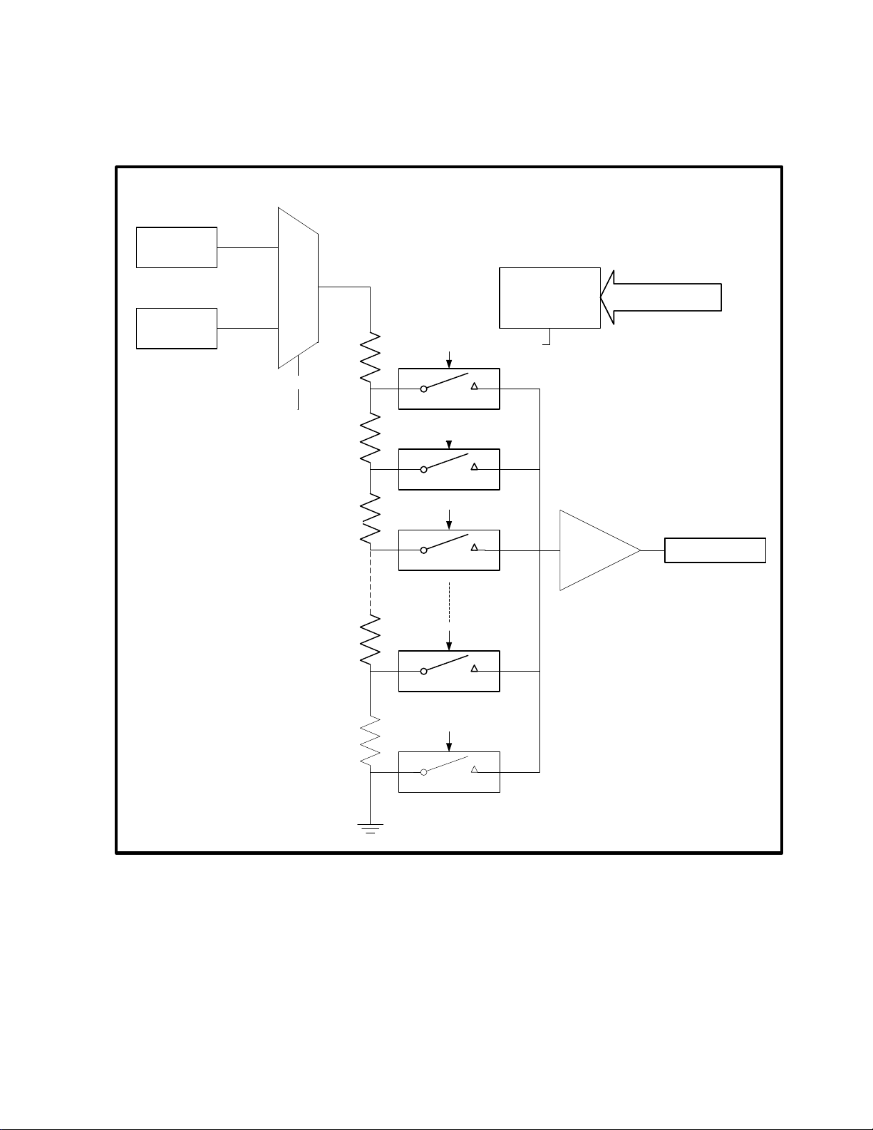
DS4830A User’s Guide
12
-Bit
Decoder
Data Bus
To DAC Switches
R
R
R
R
R
DAC Output
Internal
Reference
External
Reference
Ref Selection
4095
1
0
4094
4093
MUX
10b
01
b
Output
Buffer
SECTION 6 – DIGITAL-TO-ANALOG CONVERTER (DAC)
The DS4830A contains eight 12-bit digital-to-analog converters (DACs). Each DAC has a voltage output buffer.
Each DAC can independently select between a 2.5V internal reference and external reference at REFINA pin for
DAC0 to DAC3 and at REFINB pin for DAC4 to DAC7.
Figure 6-1: DAC Functional Diagram
6.1 – Detailed Description
The DS4830A DAC architecture consists of a resistor string with switches and decoder followed by a voltage buffer.
The DS4830A has eight independent DACs, each having the same architecture. As shown in Figure 6-1, each
DAC’s reference is software selectable. Each DAC is independently configurable using the DAC configuration and
DAC data registers. The DAC configuration register (DACCFG) provides the facility to enable or disable DACs
independently and select the reference. Each DAC can be configured for either an internal (2.5V) or an external
reference.
The DAC Data register programs the DAC for a particular voltage output depending on the value of this register and
the reference setting. The DAC outputs are voltage buffered and have the capability to sink or source current. Each
DAC output has output impedance which limits the DAC operating range if configured to sink current (refer to the
45
Page 46

DS4830A User’s Guide
Bit
15
14
13
12
11
10 9 8 7 6 5 4 3 2 1 0
Name
DACCFG7[1:0]
DACCFG6[1:0]
DACCFG5[1:0]
DACCFG4[1:0]
DACCFG3[1:0]
DACCFG2[1:0]
DACCFG1[1:0]
DACCFG0[1:0]
Reset 0 0 0 0 0 0 0 0 0 0 0 0 0 0 0 0
Access
rw
rw
rw
rw
rw
rw
rw
rw
rw
rw
rw
rw
rw
rw
rw
rw
BIT
NAME
DESCRIPTION
15:8
DACCFG7[1:0]
DAC Configuration: These bits configure DAC7-4 and select the DAC reference for
DACCFGx[1:0]
DACx Control/Reference Select
00
DACx is Disabled and is in power down mode.
01
DACx is enabled and REFINB is selected as the external reference.
register must be set to ‘1’.
10
DACx is enabled and the 2.5V Internal Reference is selected as the
DAC reference
11
Reserved. (User should not write this value+)
PIN 39 is REFINB (Port1.4).
7:0
DACCFG3[1:0]
DAC Configuration: These bits configure DAC3-0 and select the DAC reference for
DACCFGx[1:0]
DACx Control/Reference Select
00
DACx is Disabled and is in power down mode.
01
DACx is enabled and REFINA is selected as the ext ernal reference.
must be set to ‘1’.
10
DACx is enabled and the 2.5V Internal Reference is selected as the
DAC reference
11
Reserved. (User should not write this value+)
PIN 31 is REFINA (Port2.6).
DS4830A IC data sheet). The DAC output voltage is maintained during any type of reset except POR. All DACs,
REFINA and REFINB pins default to GPIO on reset.
6.1.1 – Reference Selection
Each DAC can be independently enabled with 2.5V internal reference or external reference. Each DAC has two bits
in the DAC configuration register (DACCFG) that are used to enable or disable the DAC with either an internal or an
external reference.
Any DAC can be enabled for using the internal reference by writing 10b at the corresponding location in the
DACCFG register. The internal reference automatically powers-down when none of the 8 DACs use it as a reference
source.
The external reference at REFINA (Port2.6) is selected by writing 01b at the corresponding location in the DACCFG
for DAC0-3. The REFINA automatically becomes GPIO when none of the lower 4 DACs (DAC0 to DAC3) use
REFINA as its reference. The external reference at REFINB (Port1.4) is selected by writing 01b at the corresponding
location in the DACCFG register for DAC4-7. The REFINB pin automatically becomes GPIO when none of the upper
4 DACs (DAC4 to DAC7) use REFINB as its reference. The DAC internal or external references can be measured at
the ADC. See ADC section for further detail i nformation.
6.2 – DAC Register Descriptions
The DAC module has total 9 SFR registers. These are DAC Configuration register DACCFG and 8 DAC Data
registers DACDx (DACD0 to DACD7). The DACCFG configures all DACs and the data register DACDx (DACD0DACD7) controls the corresponding DAC output vol tage. These SFRs are located in module 4.
6.2.1 – DAC Configuration Register (DACCFG)
DACCFG6[1:0]
DAC7-4 when the corresponding DAC is enabled.
DACCFG5[1:0]
DACCFG4[1:0]
To use the external reference, the REFB_CFG bit in the RPCFG
DACCFG2[1:0]
DAC3-0 when DAC enabled.
DACCFG1[1:0]
DACCFG0[1:0]
To external reference, the REFA_CFG bit in the RPCFG register
46
Page 47
Bit
15
14
13
12
11
10 9 8 7 6 5 4 3 2 1 0
Name - - - -
DACDx[11:0]
Reset 0 0 0 0 0 0 0 0 0 0 0 0 0 0 0 0
Access r r r r
rw
rw
rw
rw
rw
rw
rw
rw
rw
rw
rw
rw
BIT
NAME
DESCRIPTION
15:12
-
Reserved. The user should write zero to these bits.
11:0
DACDx
DACDx: These bits set the DACx output voltage according to reference selection
DACx Output voltage (in Volts) = (DAC Count / 4095) * Reference Voltage (in Volts)
Bit
15
14
13
12
11
10 9 8 7 6 5 4 3 2 1 0
Name - - - - - - - - - - - - - -
REFB_CFG
REFA_CFG
Reset 0 0 0 0 0 0 0 0 0 0 0 0 0 0 0 0
Access r r r r r r r r r r r r r r
rw
rw
BIT
NAME
DESCRIPTION
15:2
-
Reserved. The user should not write to these bits.
1
REFB_CFG
REFINB Pin Configuration: Setting this bit to ‘1’ configures the DAC external reference pin
for any DAC4-7 as analog input. PIN 39 is REFINB (Port1.4).
0
REFA_CFG
REFINA Pin Configuration: Setting this bit to ‘1’ configures the DAC external reference pin
for any DAC0-3 as analog input. PIN 31 is REFINA (Port2.6).
6.2.2 – DAC Data Registers (DACD0-DACD7)
*[11:0]
and reference value.
* ‘x’ = 0 to 7
6.2.3 – Reference Pin Configuration Register (RPCFG)
DS4830A User’s Guide
6.3 – DAC Code Examples
6.3.1 – DAC0 Enabled with Internal Reference and Output Voltage Configured for 50% (1.25V) of Internal
Reference
RPCFG = 0x0000;
DACCFG = 0x0002; //Only DAC0 enabled and internal reference is selected
DACD0 = 0x0800; //DACD0 is set for 50%
6.3.2 – DAC2 Enabled with External Reference And Output Voltage Configured for 25% of External Reference
at REFINA Pin
RPCFG = 0x0001;
DACCFG = 0x0010; //Only DAC2 enabled and ext ernal reference is selected
DACD2 = 0x0400; //DACD2 is set for 25%
6.3.3 – DAC6 Enabled with External Reference and Output Voltage Configured for 25% of External Reference
at REFINB Pin
RPCFG = 0x0002;
DACCFG = 0x1000; //Only DAC6 enabled and ext ernal reference is selected
DACD6 = 0x0400; //DACD6 is set for 25%
47
Page 48

DS4830A User’s Guide
13-BIT ADC CORE
ADC-S0
ADC-S1
ADC-S14
ADC-S15
A
N
A
L
O
G
M
U
X
VOLTAGE OFFSET
(ADVOFF)
INTERNAL DIE TEMP
Current Source
For Temperature
Measurement
ADC SEQUENCER
ADSTART
ADEND
ADCONV
ADCONT
ADCG1
ADCG
4
ADGAIN
INTERNAL
REFERENCE
CONFIGURATION[0]
CONFIGURATION[19]
CONFIGURATION[1]
DATA BUFFER[0]
DATA BUFFER[24]
DATA BUFFER[1]
ADCFG=0
ADIDX[4:0]
READ
ADDATA
ADCG
3
ADCG2
REFINA
REFINB
DAC INT REF
VDD
Reserved
Reserved
SH0
SH1
Internal Offset
NUM
_SMP
CONFIGURATION[23]
DIGITAL
READOUT
ADCFG=1
ADIDX[4:0]
ADCAVG=1
ADIDX[4:0]
WRITE TO ADDATA
ADC SEQ
ADC AVG
REFAVG
SECTION 7 – ANALOG-TO-DIGITAL CONVERTER (ADC)
The DS4830A provides a 13-bit analog-to-digital converter (ADC) with 26-input MUX. As shown in Figure 7-1, the
MUX selects the ADC input from 16 external channels, DAC external references at REFINA and REFINB, V
Internal Reference, Internal Die Temperature, Sample and Hold at GP2-GP3 and GP12-GP13 and ADC Internal
Offset. The ADC external channels can operate in differential voltage mode or in single-ended voltage mode. An
internal channel is used exclusively to measure the die temperature. The REFINA and REFINB pins can be used as
analog channel independent to the DAC reference.
DD, DAC
Figure 7-1: ADC Functional Diagram
7.1 – Detailed Description
7.1.1 – ADC Controller
The ADC controller is the digital interface block between CPU and the ADC. It provides all necessary controls to the
ADC and the CPU interface. The ADC controller provides 25 buffers (0-24) for various configurations and data
buffers. By default, the ADC conversion result corresponding to each channel is placed in data buffers at the location
shown in Table 7-1. The user can override the default buffer locations and define alternate locations in the ADC Data
and Configuration register (ADDATA) during configuration by settling the LOC_OVR bit to ‘1’ in the ADC Control
register (ADCN). The internal temperature sensor and Sample and Hold (S/H) use fixed data buffer locations and
these locations should not be used for other channels if these peripherals are enabled. The ADC internal offset does
not have any data buffer and its measurement is performed with location override enable. Table 7-1 has the default
configuration and data buffer locations. The ADC controller provides various internal averaging options for individual
ADC channels, internal die temperature and S/H. See Section 7.1. 9 for ADC Averaging.
48
Page 49

DS4830A User’s Guide
DATA BUFFER
CONFIGURATION/DATA BUFFE R SELECTION
0-15
External Channels (0-15 in single-ended or 0-7 in differential)
16
REFINA
17
REFINB
18
VDD (Supply Voltage)
19
DAC Internal Reference
20-21
Reserved, can be used with Location Override
22
Internal Die Temperature
23
Sample and Hold 0
24
Sample and Hold 1
0-24 (Any)
ADC Internal Offset (with Location Override)
Table 7-1: ADC Configuration and Data Buffers
By default, the external channels GP0-15 are general-purpose inputs. The DS4830A has the Pin Select Register
(PINSEL) which is used to configure these external channels as analog pins for ADC or/and Quick Trip use. Each bit
location in this register corresponds to the ADC/QT input pin. The ADC controller uses a set of Special Function
Registers (SFRs) to configure the ADC for the desired mode of operation. The DS4830A ADC can operate in the
three modes mentioned below.
1. ADC Sequence Mode Conversions
2. Temperature Mode Conversions
3. Sample and Hold Mode Conversions
7.1.2 – ADC Conversion Sequencing
The DS4830A ADC controller performs a user defined sequence for up to 16 single-ended or 8 differential external
voltage channels. Additionally, the ADC controller allows the user to measure voltages of the DAC internal and
external references (REFINA and REFINB) and V
independent of DAC operation. Thus the DS4830A provides 18 analog channels for application usage. The ADC
controller provides 24 ADC internal configuration and averaging configuration registers. The configuration registers
are accessed by writing to the ADDATA register when ADST.ADCFG = 1 and ADST.ADCAVG = 0. The averaging
configuration registers are accessed by writing to the ADDATA register when ADST.ADCAVG = 1 and
ADST.ADCFG = 0. Each conversion in a sequence is setup using one of the ADC configuration and averaging
configuration registers. The results from the ADC converter are located in the 25 data buffers. These are accessed
by reading from the ADDATA register when ADST.ADCFG = 0 and ADST.ADCAVG = 0. See Figure 7-2 for ADC
configurations and data buffers.
The configuration register pointed to by ADDATA is selected using the ADIDX bits in the ADST register when
ADCFG = 1 and ADCAVG = 0. The individual configuration registers allows each of the conversions in a sequence
to select from the following options.
• ADC channel selection
• Differential or single-ended conversion
• Full scale range
• Extended acquisition enable
• ADC conversion data alignment (left or right )
• Alternate location
For more information, see the configuration register description for the ADDATA register.
A sequence is setup in the ADC Address register (ADADDR) by defining the starting conversion configuration
address (ADSTART) and an ending conversion configuration address (ADEND). The configuration start address
designates the configuration register to be used for the first conversion in a sequence. The configuration end
address designates the configuration register used for the last conversion in a sequence. A single channel
conversion can be viewed as a special case for sequence conversion, where the starting and ending configuration
address is the same. The configuration registers can be viewed as a circular register array where ADSTART does
not have to be less than ADEND. For example, if ADSTART = 1 and ADEND = 5, then the sequence of conversions
would be configurations 1, 2, 3, 4, 5. If ADSTART = 5 and ADEND = 1, then the sequence of conversions would be
configurations 5, 6, 7 . . . 23 , 0, 1.
The ADC has two conversion sequence modes, single and continuous which are set by the ADCONT bit. When the
start conversion bit (ADCONV) is set to ‘1’, the ADC controller starts the ADC conversion sequence. In single
sequence mode (ADCONT=0), the ADCONV bit remains set until the ADC has finished the conversion of the last
channel in the sequence. In continuous mode (ADCONT=1), the ADCONV bit remains set until the continuous mode
DD . The REFINA and REFINB can be used as analog channels
49
Page 50

DS4830A User’s Guide
ADCFG = 0
ADCAVG =
0
Data Buffer[
0]
Data Buffer[
23
]
Data Buffer[1]
Data Buffer
[24]
DATA BUFFERS
CONFIGURATION[
0]
CONFIGURATION[22
]
CONFIGURATION[
1]
CONFIGURATION
[23]
ADC CONFIGURATIONS
ADIDX
[4:
0]
ADCFG
= 1
ADCAVG =
0
ADIDX[
4:0
]
CONFIGURATION
[
0]
CONFIGURATION
[
22]
CONFIGURATION
[1
]
CONFIGURATION
[23
]
ADC AVERAGE
CONFIGURATIONS
ADCAVG
= 1
ADCFG
=
0
ADIDX[
4
:0
]
is stopped. Writing a ‘0’ to the ADCONV bit stops the ADC operation at the completion of the current ADC
conversion. Writing a ‘1’ to the ADCONV bit when ADCONV bit is already set to ‘1’ is ignored by the ADC controller.
Figure 7-2: ADC Configurations and Data Buffers
Note: With location override enabled, a single channel can be added multiple times as demonstrated in Example
7.3.2.
7.1.3 – Internal Die Temperature Con version
The DS4830A allows monitoring of internal die temperature. The internal temperature channel can be independently
enabled by writing a ‘1’ to the bit 0 in the Temperature Control register (TEMPCN). The internal die temperature has
a temperature conversion complete flag located in the ADST register. Data buffer 22 is reserved for the result of the
internal die temperature sensor. The TEMPCN register has separate bits for interrupt enabl e and data alignment.
A DS4830A temperature conversion provides 0.062 °C of resolution. The time required for a temperature conversion
is approximately 42µsec at the default ADC Clock. If temperature conversion is enabled simultaneously with voltage
conversions, the temperature conversion gets time slots at the end of ADC sequence. See Figure 7-3 ADC Frame
Sequence for more details.
Note: If only internal temperature conversions are being performed (no voltage or sample/hold conversions are
enabled), to disable the temperature conversion, a dummy ADC conversion must be performed by setting
ADCONV=1.
50
Page 51

DS4830A User’s Guide
CH0 CH
4 S/
H1 CH
5 S/
H0 CH6
Int
Temp
CH0
S/H
1 CH4 ……
..……..
Every alternate
channel is primary
channel
Both S/H
0 & S/
H1
are ready. S
/H0
gets priority over
S/H
1
S/H
1 gets
chance here
even if S/H0
is ready.
Sequence
keeps
repeating
SH
0 or
1 if
triggered by
internal or
SHEN
0/
1
l
S/
H0
End of Sequence.
Internal
Temperature gets
chance here.
7.1.4 – Sample and Hold Conversion
The DS4830A has two Sample and Hold (S/H) inputs at pins GP2-GP3 and GP12-GP13. These can be
independently enabled or disabled by writing to their corresponding bit locations in the Sample and Hold Control
register (SHCN). See the Sample and Hold description in Section 8. The Sample and Hold uses data buffer 23 and
24 for S/H0 and S/H1 respectively. The Sample and Hold conversion complete flags are located in the ADST
register. When enabled with voltage conversions, the sample and hold conversions get time slots in between each
voltage conversion. See Figure 7-3, ADC Frame Seq uence for more details.
7.1.5 – ADC Frame Sequence
When all modes (voltage, temperature, and sample and hold) are used simultaneously, the ADC controller uses time
slicing. The ADC controller uses the ADC sequence of voltage conversions as “primary channels” and sample and
hold as secondary channels. The time slicing rules are
1. The primary channels (ADC voltage channels) have priority over the secondary channel s (S/Hs).
2. S/H0 has priority over S/H1 if both S/Hs are ready for conversion. However, in next slot for S/H, the S/H1 will
get slot even if S/H0 is also ready.
3. The internal die temperature gets the conversion slots at the end of ADC sequence.
For example, if the ADC sequence mode conversion is enabled for channel 0, 4, 5, 6, both S/Hs and internal die
temperature are enabled and ready for conversion then the sequence of conversion is performed as shown in Figure
7-3.
Figure 7-3: ADC Frame Sequence
Notes:
1. Both Sample and Hold channels can occur simultaneously as they have dedicated resources.
2. Averaging is disabled.
7.1.6 – ADC Reference
The ADC has a 1.2V internal reference that must be enabled before the start of ADC conversion sequence. The
ADC controller provides INT_REF bit in the REFAVG register to control the ADC internal reference. By setting this bit
to ‘1’, the internal reference is enabled. The ADC internal reference needs approximate 1ms of stabilization time. The
ADC conversion should be started only after this stabilization time.
The ADC controller provides an option to bring out the ADC internal reference at GP1 pin (PIN6, Port2.1). By setting
REF_OUT bit in the REFAVG register and the bit 1 of the PINSEL register, the ADC internal reference is brought out
at GP1 pin.
51
Page 52

DS4830A User’s Guide
7.1.7 – ADC Conversion Time
The ADC clock is derived from the system clock with a divide ratio defined by the ADC Clock Divider Bits ADCCLK
[2:0] in the ADC Control register (ADCN). Each sample takes 15 ADC clock cycles to complete. Two of the 15 ADC
clock cycles are used for sample acquisition, and the remaining 13 clocks are used for data conversion. The ADC
automatically reads each measurement twice and outputs the average of the two readings. This makes the resulting
time for one complete conversion to be 30 ADC clock cycles. Additionally, 4 core clocks are used in data processing
for each of the two readings.
Knowing this, it is possible to calculate the f ast est ADC sample rate. The fastest ADC clock is:
ADC Clock = Core Clock / 8 = 10 MHz / 8 = 1250 kHz = 0.8 µs
One conversion requires 30 ADC Clocks + 8 C ore Clocks
Conversion Time = (30 ADC Clocks Time+ 8 Core Clocks Time)
= 30 * 0.8 + 0.8 µs
= 24.8 µs per ADC Conversion
Sample Rate = 40.3 ksps
The ADC has an internal power management system that automatically shuts down the ADC when conversions are
complete by clearing ADCONV to 0. After being shut down, the ADC begins conversions again when the ADCONV
bit is set to 1 again. After ADCONV is set to 1, the ADC requires 20 ADCCLK cycles to setup and power up prior to
beginning the first conversion of the sequence. So the first ADC conversion time is ~40µs at the fastest ADC Clock.
If the quick trip is also enabled and if the ADC controller and the quick trip are sampling the same channel, the ADC
sampling is delayed by two quick trip conversions (3.2µs) to prevent collision.
In applications where extending the acquisition time is desired, the user can make use of the ADC Acquisition
Extension Bits (ADACQ[3:0] in the ADCN register). When the ADC Acquisition Extension is enabled (ADACQEN=1),
the sample is acquired over a prolonged period during the sample acquisition. The extended acquisition time is
determined by ADACQ[3:0]. Table 7-2 shows the extended acquisition time in terms of core clocks at different
ADACQ[3:0] The total acquisition time, ACQ, is two ADC clocks plus the Extended Acquisition Time (ADACQ, as
listed in Table 7-2). Figure 7-4 shows the clocking required for one co nversion.
Table 7-2: Extended Acquisition Time in Terms of Core Clock and Time (µs)
ADACQ[3:0] # of Core Clocks Time (µs)
0 2 0.2
1 6 0.6
2 14 1.4
3 30 3.0
4 62 6.2
5 126 12.6
6 254 25.4
7 520 52
8 1032 103.2
9 2056 205.6
10 4104 410.4
11 8190 819
12 16382 1638.2
13 32766 3276.6
14 65534 6553.4
15 131070 13107
52
Page 53

10 111 2 3 4 5 6 7 8 9 181615141312
28 2919 20 21 22 23 24 25 26 2717 30
...
1 19 20
ADACQ
SAMPLE 1
HOLD AND CONVERT SAMPLE 1
SAMPLE 2
HOLD AND CONVERT SAMPLE 2
ADC
STARTUP
ADC DATA
VALID
ADCCLK
ADCONV
ADDATA
Core Clock
delays
(ADACQ[3:0])
DS4830A User’s Guide
Figure 7-4: Extended Acquisition Time
7.1.8 – Location Override
By default, the ADC controller stores ADC conversion results in the ADC buffer location corresponding to the
channel number (as defined in Table 7.1). The ADC controller allows the user to override the default data buffer
location and store the ADC result at any of the buffer location (0-24). The location override is enabled by setting the
LOC_OVR bit to ‘1’ in the ADCN register. The user has to define the alternate location for storing the ADC
conversion result during ADC configuration (when ADST.ADCFG = 1). The alternate location is defined by
ADDATA[12:8] (ALT_LOC). Location override is demonstrated in Example 7.3.2,
Note: If the location override will be using the buffer locations designed for internal temperature or sample and hold,
these corresponding peripherals should be disabled (as mentioned in 7.1.1). Example, if the buffer location 22 is
used in the ADC sequence with the location overri de option, the internal die temperature should be disabled.
7.1. 9 – Averaging
The ADC controller supports various averaging options for each ADC channel, internal die temperature and S/Hs.
This averaging is performed automatically by the ADC controller which reduces application overheads. The ADC
controller has ADCAVG bit in the ADST register which is used to configure number of ADC samples to be averaged
for each channel. When the ADCFG bit is set to 0 and ADCAVG bit is set to ‘1’, writing to ADDAT A [1:0] configures
the number of ADC samples to be averaged. User can write any value between 0-3 to select 1, 4, 8 or 16 ADC
samples averaged. See Section 7.1.2 for averaging configuration register and 7.3.3 for ADC averaging example
code.
The ADC controller has the REFAVG register to configure different averaging options for internal die temperature
and S/H. Each sample of the internal temperature is converted after the ADC sequence. See the REFAVG register
description for detailed information about averaging options for internal die temperature and sample and hold
channels.
When averaging configuration is enabled in the ADC sequence for ADC channels, internal die temperature and
S/Hs, the ADC frame sequence is changed and explained in Figure 7-5. The ADC and S/H samples are converted
back to back by the ADC controller and averaged values are reported in the data buffers. After every end of
sequence, the ADC controller converts a sample of internal die temperature.
53
Page 54

DS4830A User’s Guide
CH0
(4)
CH4
(8)
S/H1
(4)
CH5
(16)
S/H0
(2)
CH6
(1)
Int
Temp
(1)
CH0
(4)
……..
……..
Every alternate
channel is
primary channel
Both S/H0 & S/H1 are ready. S/
H0 samples will get converted
by ADC and average value is
reported.
S/H1 samples
will get
converted by
ADC.
Sequence
keeps repeating
SH0 or 1 if
triggered by
internal or
SHEN0/1l
S/H0
(2)
End of Sequence.
One Sample of
Internal Temperature
gets chance here.
CH0
samples get
converted
by ADC
t = 0
t = 144µs
t = 216µs
t = 504µs
t = 648µs
t = 1224µs
t = 1338µs
t = 1296µs
t = 1332µs
t = 1512µs
Note: Conversion time is using the default clock.
ADDAINV
SET ADDAI AFTER
0
End of Every Sequence (ADSTART to ADEND)
After End of Every Sequence (ADSTART to ADE ND) and After
(NUM_SMP + 1) ADC Conversions
Figure 7-5 shows the ADC frame sequence for the f ollowing programmed sequence of ADC channels.
1. CH0: Average of 4 Samples
2. CH4: Average of 8 Samples
3. CH5: Average of 16 Samples
4. CH6: Average of 1 Sample
5. S/H0: Average of 2 Samples
6. S/H1: Average of 4 Samples
7. Internal Temperaute: Average of 16 Samples
Figure 7-5: ADC Frame Sequence with Averaging
7.1.10 – ADC Data Reading
The ADC has a circular data buffer that can hold the results from 25 conversions. When the location override
(LOC_OVR = 0) is disabled, the ADC controller writes the ADC conversion result at the data buffer location
corresponding to ADC channel number, see Table 7-1. When location override is enabled, the ADC controller writes
the result to the data buffer location configured in the ALT_LOC[4:0] bits in the ADDATA during ADC configuration
(ADST.ADCFG = 1). Using the location override feature, multiple conversions for a single channel can be stored to
data buffers as explained in example code 7.3.2. This buffer is accessed by reading the ADDATA register when
ADCFG is set to 0. The data buffer pointed to by ADST.ADIDX [4:0] is the buffer returned when ADDATA is read.
The ADIDX is automatically incremented following a read of ADDATA. This allows repeated reads of ADDATA to
return the results from multiple conversions. The ADC continues writing to the data buffer until the end of the buffer.
Once the end of the data buffer is reached, the ADC index rolls over and reading continues from data buffer 0.
7.1.11 – ADC Interrupts
The ADC Data Available Ready ADDAI bit in the ADST1 register is set when conversions are complete. This flag
generates an interrupt if enabled by setting the ADCN.ADDAIE interrupt enable bit. The condition that causes the
ADDAI flag to be set can be selected using the ADC N.ADDAINV bit.
Table 7-3: ADC Interrupt Intervals
1
54
Page 55

DS4830A User’s Guide
SAMPLE0 SAMPLE1 SAMPLE2 SAMPLE3 SAMPLE4 SAMPLE5
SAMPLE6 SAMPLE0 ……...
ADDAI Set
After
(NUM_SMP + 1)
ADC Samples
ADDAI Set
After END of
Sequence
4 ADC Samples 4 ADC Samples
ADDAI Set
After
(NUM_SMP + 1)
ADC Samples
ADC
SAMPLES
ADDAI
Flag
For example, if ADSTART = 0, ADEND = 6 and NUM_SMP = 3 with ADDAINV = 1, then ADDAI is s et to ‘1’ after
every (NUM_SMP + 1) ADC conversions and every End of Sequence. In the given example, ADDAI is set after
4,7,8,12,14… ADC Samples. Interrupts after 4, 8 and 12 ADC Samples are because of (NUM_SMP+1)
configurations and interrupts after 7 and 14 are because of “End of Sequence”. Figure 7-6 demonstrates above ADC
example sequence.
If ADC averaging is used, each of the converstions for an average is counted as a sample for interrupts. For
example, if four samples are being averaged for each channel and interrupts are set to trigger every four
converstions, then an interrupt will occur af ter each channel completes its four samples.
Figure 7-6: ADC Interrupt Intervals with NUM_SMP
The ADDAI flag is cleared by software by writing a ‘0’, or it is automatically cleared when a new conversion
sequence is started by setting the ADCONV bit to a ‘1’.
Note: The ADC controller processes ADC, internal die temperature and sample and holds conversions according to
ADC frame sequence and sets the corresponding flags in the ADST1 flag. The user should process and clear an
interrupt flag when it is set before another flag in the ADST1 is set by the ADC controller.
7.1.12 – ADC Internal Offset
The DS4830A ADC controller allows for ADC internal offset measurement. The ADC controller does not have a
dedicated buffer for the internal offset so it can only be accessed with location override enabled. For measurement of
ADC internal offset, the ADC controller connects internal ground to the ADC input and performs an ADC conversion.
Using this feature, software can calibrate the ADC internal offset.
Refer to Application Note 5321: Calibrating the ADC Internal Offset of the DS4830 Optical Microcontroller
.
7.1.13 – DAC External Reference Pins (REFINA and REFINB) as ADC Channels
The DS4830A provides an option to measure the voltage applied to the DAC external reference pins REFINA and
REFINB without enabling any DACs. The ADC controller has RPCFG register to configure REFINA and REFINB as
analog pins. This allows flexibility to use the REFINA and REFINB pins as two additional analog input channels and
can also be used as DAC external reference.
7.1.14 – Fast Conversion Mode (ADST.ENABLE_2X)
The DS4830A ADC controller can be used in fast mode to reduce the sample conversion time. The Enable_2x bit in
ADST register has to be set to 1 to use the ADC in fast mode. In normal operating mode, the ADC reads two input
samples and outputs the average of the results of both the samples. In Fast conversion mode, the ADC reads only
one input sample and outputs the result as such. The ADC conversion time is reduced by half when operating in fast
mode.
55
Page 56

DS4830A User’s Guide
Bit
15
14
13
12
11
10 9 8 7 6 5 4 3 2 1 0
Name
ADCCLK[2:0]
NUM_SMP[4:0]
ADDAINV
ADCONT
ADDAIE
LOC_OVR
ADACQ[3:0]
Reset 0 1 0 0 0 0 0 0 0 0 0 0 0 0 0 0
Access
rw*
rw*
rw*
rw*
rw*
rw*
rw*
rw*
rw*
rw*
rw*
rw*
rw*
rw*
rw*
rw*
BIT
NAME
DESCRIPTION
15:13
ADCCLK[2:0]
ADC Clock Divider. These bits select the ADC conversion clock in relationship to the
ADCCLK[2:0]
ADC Clock
000
System Clock/8
001
System Clock/10
010
System Clock/12
011
System Clock/14
100
System Clock/16
101
System Clock/18
110
System Clock/20
111
System Clock/40
12:8
NUM_SMP[4:0]
Interrupt After Number of Sample. These bits define the Number of ADC samples
Interrupt occurs after (NUM_SMP + 1) ADC samples and End of Sequence.
7
ADDAINV
ADC Data Available Interrupt Interval. This bit selects the condition for setting the
(NUM_SMP + 1).
6
ADCONT
ADC Continuous Sequence Mode. Setting this bit to ‘1’ enables the continuous
the continuous sequence mode. In
The user should set this bit to ‘1’, when temperature and sample and hold are also
enabled.
5
ADDAIE
ADC Data Available Interrupt Enable. Setting the ADDAIE bit to ‘1’ enables an
interrupt from generating when ADDAI=1. This bit is unconditional writable.
4
LOC_OVR
Location override bit. Setting this bit to ‘1’ enables the user to select an alternate
location is defined by
buffer location corresponding to channel number. See Table 7-1.
3:0
ADACQ[3:0]
ADC Acquisition Extension Bits [3:0]. These bits are used to extend sample
acquisition time if the corresponding ADC Acquisition Extension is enabled
The ADC acquisition extension should not be used when the fast
comparator is used for the same channel.
7.2 – ADC Register Descriptions
The ADC is controlled by the ADC SFR registers. The PINSEL register is used to configure pins as analog pins for
ADC use. Six of the registers, ADST, ADST1, ADADDR, ADCN, RPCFG, REFAVG and ADDATA are used for
setup, control, and reading from the ADC. Registers ADCG1-4 and ADVOFF which are used to adjust the gains and
offsets applied to ADC results. To avoid undesired operations, the user should not write to bits labeled as
“Reserved”.
7.2.1 – ADC Control Register (ADCN )
* Unrestricted read, but can only be written to whe n ADCONV = 0 except ADDAIE bit.
Core Clock.
required for an ADC interrupt when ADDAINV = 1. If ADDAINV is set to ‘1’, then ADC
data available interrupt flag (ADDAI).
When ADDAINV = 0, ADDAI is set after End of Sequence.
When ADDAINV = 1, ADDAI is set after End of Sequence and after ADC Samples =
sequence mode. Clearing this bit to ‘0’ disables
single sequence mode, the ADC conversion is stopped after the end of the sequence.
interrupt to be generated when the ADDAI=1. Clearing this bit to ‘0’ disables an
location for storing ADC conversion results. The alternate
ADDATA[12:8] (ALT_LOC). By default, the ADC conversion results are stored in ADC
(ADDATA.ADACQEN =1 when ADST.ADCFG is set to ‘1’). See ADC Conversion Time
Section for details.
56
Page 57

Bit
15
14
13
12
11
10 9 8 7 6 5 4 3 2 1 0
Name - - - -
ENALE_2X
- - -
ADCAVG
ADCONV
ADCFG
ADIDX[4:0]
Reset 0 0 0 0 0 0 0 0 0 0 0 0 0 0 0 0
Access r r r r
rw r r r rw
rw
rw
rw
rw
rw
rw
rw
BIT
NAME
DESCRIPTION
15:12
-
Reserved. The user should not write to these bits.
11
ENABLE_2X
ADC Fast Conversion Mode. When ADST.ENABLE_2X = 1, the ADC operates in the
fast mode. If reset to 0, normal conversion mode is used.
7
ADCAVG
ADC Average Configuration Register Select.
channel. See 7.2.6.2 for ADC sample average configurati ons.
6
ADCONV
ADC Start Conversion. Setting this bit to ‘1’ starts the ADC conversion process. This
acquiring data after the
the ADC stops immediately.
5
ADCFG
ADC Conversion Configuration Register Select.
ADCFG = 0: The ADDATA register points to the data buffers. The ADIDX[4:0] bits
ADCFG = 1: The ADDATA register points to the ADC sequence configuration registers.
The ADIDX[4:0] bits determine which configuration register is currently being accessed.
When ADCFG=1, ADDATA has read/write acce ss.
4:0
ADIDX[4:0]
ADC Register Index Bits [4:0]. These bits together with ADCFG and ADCAVG select
ADCFG=0, ADCAVG=0: ADIDX[4:0] used to select one of 25 data buffers.
Bit
15
14
13
12
11
10 9 8 7 6 5 4 3 2 1 0
Name
PINSEL[15:0]
Reset 0 0 0 0 0 0 0 0 0 0 0 0 0 0 0 0
Access
rw
rw
rw
rw
rw
rw
rw
rw
rw
rw
rw
rw
rw
rw
rw
rw
7.2.2 – ADC Status Register (ADST)
When ADCAVG = 1 and ADCFG = 0, the ADDATA register points to the ADC Channel
averaging configuration registers which allow configuration of averaging for each ADC
bit remains set until the ADC conversion process is finished. In single sequence mode,
this bit is cleared to ‘0’ when the ADC conversion sequence is finished. In continuous
sequence mode, this bit remains set until the ADC conversion is stopped. To stop ADC
conversion at any time, write ‘0’ to this bit. The ADC stops
current conversion is finished or if the ADC is waiting during extended acquisition time,
DS4830A User’s Guide
determine which data buffer is currently being accessed. When ADCFG=0 and
ADCAVG = 0, ADDATA is read only.
the source / destination for ADDATA access. This register value is auto-incremented on
successive access (read/write) of ADDATA register. When ADCFG=1, ADIDX [4:0] are
used to address one of 24 configuration registers. When ADCFG=0, ADIDX [4:0] are
used to select one of 25 data buffers.
ADCFG=1, ADCAVG=0: ADIDX[4:0] used to address one of 24 configuration registers
ADCFG=0, ADCAVG=1: ADIDX[4:0] used to address one of 24 average configurations
7.2.3 – PIN Select Register (PINSEL)
Each bit in this register corresponds to an ADC input pin. When these bits are set the corresponding pins are
dedicated for ADC use. On POR, the pin selection register is 0000h which corresponds to GP0 to GP15 being GPIO.
For using these pins as ADC input, Sample and Hold or Quick Trip inputs the corresponding PINSEL bit should be
set to ‘1’.
57
Page 58

Bit
15
14
13
12
11
10 9 8 7 6 5 4 3 2 1 0
Name - - - - - - - - -
SH1DAI
SH0DAI - -
INTDAI
ADDAI
Reset 0 0 0 0 0 0 0 0 0 0 0 0 0 0 0 0
Access r r r r r r r r r r
rw
rw r r
rw
rw
BIT
NAME
DESCRIPTION
15:6
-
Reserved. The user should not write to these bits.
5
SH1DAI
Sample and Hold 1 Data Available Interrupt Flag. This bit is set to ‘1’ when Sample
cleared by software writing a ‘0’.
4
SH0DAI
Sample and Hold 0 Data Available Interrupt Flag. This bit is set to ‘1’ when Sample
SH0DAI_EN (SHCN.1) is set to ‘1’. This bit is cleared by software writing a ‘0’.
3:2 - Reserved. The user should not write to these bits.
1
INTDAI
Internal Temperature Data Available Interrupt Flag. This bit is set to ‘1’ when an
software writing a ‘0’.
0
ADDAI
ADC Data Available Interrupt Flag. This bit is set to ‘1’ when the condition matching
cleared by software writing a ‘0’ or when software changes ADCONV bit from '0' to ‘1’.
Bit
15
14
13
12
11
10 9 8 7 6 5 4 3 2 1 0
Name - -
-
ADSTART[4:0]
- - -
ADEND[4:0]
Reset 0 0 0 0 0 0 0 0 0 0 0 0 0 0 0 0
Access r r r rw*
rw*
rw*
rw*
rw* r r r rw*
rw*
rw*
rw*
rw*
BIT
NAME
DESCRIPTION
15:13
-
Reserved. The user should not write to these bits.
12:8
ADSTART[4:0]
ADC Conversion Configuration Start Address Bits [4:0]. These bits select the first
7:5 - Reserved. The user should not write to these bit s.
4:0
ADEND[4:0]
ADC Conversion Configuration Ending Address Bits [4:0]. These bits select the
last conversion configuration register. This register is inclusive when defining the
sequence.
7.2.4 – ADC Status Register (ADST1)
and Hold is completed on GP12-GP13 in dual mode and data is ready at buffer location
24. This flag causes an interrupt if the SH1DAI_EN (SHCN.5) is set to ‘1’. This bit is
and Hold is completed on GP2-GP3 if only S/H0 is used or after completion of S/H1
conversion on GP12-GP13 when both are used in single mode. The S/H0 and S/H1 data
is ready at buffer location 23 and 24 respectively. This flag causes an interrupt if the
internal temperature conversion is complete and data is ready in buffer location 22. This
flag causes an interrupt if the INT_IEN (TEMPCN.10) is enabled. This bit is cleared by
DS4830A User’s Guide
ADDAINV bit is met. This flag causes an interrupt if the ADDAIE bit is set. This bit is
7.2.5 – ADC Address Register ( ADADDR)
* Unrestricted read, but can only be written to whe n ADCONV = 0.
conversion configuration register.
7.2.6 – ADC Data and Configuration Register (ADDATA)
The ADDATA register is used to setup the ADC sequence configurations and also to read the results of the ADC
conversions. If the ADST.ADCFG bit is set to a 1 and ADST.ADCAVG = 0, writing to ADDATA writes to one of the
configuration registers. If ADST.ADCFG is set to 0 and ADST.ADCAVG is set to 1, writing to ADDATA writes to one
of the averaging configuration registers. If ADST.ADCFG and ADST.ADCAVG is set to 0, reading from ADDATA
reads one of the conversion results.
58
Page 59

DS4830A User’s Guide
Bit
15
14
13
12
11
10 9 8 7 6 5 4 3 2 1 0
Name
-
ADGAIN[1:0]
ALT_LOC[4:0]
ADACQEN
ADALIGN
ADDIFF
ADCH[4:0]
Reset
0 0 0 0 0 0 0 0 0 0 0 0 0 0 0
0
Access
r
rw*
rw*
rw*
rw*
rw*
rw*
rw*
rw*
rw*
rw*
rw*
rw*
rw*
rw*
rw*
BIT
NAME
DESCRIPTION
15 - Reserved. The user should not write to this bit.
14:13
ADGAIN[1:0]
ADC Gain Select. This bit selects the A DC scale factor.
ADGAIN[1:0]
ADC SCALE
Full Scale (typ)
00
ADCG1
1.2V
01
ADCG2
0.6V
10
ADCG3
2.4V
11
ADCG4
6.55*
operating range.
12:8
ALT_LOC[4:0]
Alternate location for conversion result. These bits specify the alternate location for
storing the ADC conversion result when LOC_ O V R bit in the ADCN register is set to ‘1’.
7
ADACQEN
ADC Acquisition Extension Enable. Setting this bit to ‘1’ enables additional acquisition
acquisition time.
6
ADALIGN
ADC Data Alignment Select. This bit selects the ADC data alignment mode. Setting this
ADDATA[15:14] sign-extended by ADDATA[13].
5
ADDIFF
ADC Differential Mode Select. This bit selects the ADC conversion mode. When this bit
is set to ‘1’, the ADC conversion is in differential mode. When this bit is cleared to ‘0’, the
measured between the ADC Channel and ground.
4:0
ADCH[4:0]
ADC Channel Select. These bits select the input channel source for configuration of ADC
ADCH [4:0]
ADDIFF = 0
ADDIFF=1
00000
ADC-S0
ADC-D0P- ADC-D0N
00001
ADC-S1
ADC-D1P- ADC-D1N
00010
ADC-S2
ADC-D2P- ADC-D2N
00011
ADC-S3
ADC-D3P- ADC-D3N
00100
ADC-S4
ADC-D4P- ADC-D4N
00101
ADC-S5
ADC-D5P- ADC-D5N
00110
ADC-S6
ADC-D6P- ADC-D6N
00111
ADC-S7
ADC-D7P- ADC-D7N
01000
ADC-S8
NOT VALID
01001
ADC-S9
NOT VALID
01010
ADC-S10
NOT VALID
01011
ADC-S11
NOT VALID
01100
ADC-S12
NOT VALID
01101
ADC-S13
NOT VALID
01110
ADC-S14
NOT VALID
01111
ADC-S15
NOT VALID
10000
ADC-REFINA
ADC-REFINA
10001
ADC-REFINB
ADC-REFINB
10010
VDD
VDD
10011
DAC_INT_REF
DAC_INT_REF
10100- 11000
NOT VALID
NOT VALID
11001
ADC OFFSET
ADC OFFSET
7.2.6.1 – ADC Configuration Register (ADDATA when ADCFG = 1 and ADCAVG = 0)
When ADCFG = 1 and ADCAVG = 0, writing to the ADDATA reg ister writes to one of the configuration registers.
The configuration register written to is selected by the ADIDX[4:0] bits. The ADIDX[4:0] bits are automatically
incremented after a write to ADDATA. This allows consecutive writes of ADDATA to setup consecutive configuration
registers. The configuration registers are reset to ‘0’ on all forms of reset.
* When ADCFG = 1, unrestricted read, but can only be written to when ADCONV = 0.
* When the ADCG4 select, the ADC input should not be above 3.6V. It is limited by VDD
time to be inserted prior to this conversion. Clearing this bit to ‘0’ disables the extended
bit to ‘1’ returns ADC data left aligned in ADDATA [15:2] with ADDATA[1:0] zero padded.
Clearing this bit to ‘0’ returns ADC data in right aligned format in ADDATA[13:0] with
ADC conversion is performed in single-ended mode. In single-ended mode, the sample is
conversion.
59
Page 60
DS4830A User’s Guide
Bit
15
14
13
12
11
10 9 8 7 6 5 4 3 2 1 0
Name - - - - - - - - - - - - - -
AVG[1:0]
Reset 0 0 0 0 0 0 0 0 0 0 0 0 0 0 0 0
Access r r r r r r r r r r r r r r
rw*
rw*
BIT
NAME
DESCRIPTION
15:2
-
Reserved. The user should not write to these bits.
1:0
AVG[1:0]
ADC Average Select: These bits select number of ADC samples to be averaged by the
AVG[1:0]
Samples Average
00 1 01
4
10
8
11
16
Bit
15
14
13
12
11
10 9 8 7 6 5 4 3 2 1 0
Temperature Right Aligned
S S S
28
27
26
25
24
23
22
21
20
2-1
2-2
2-3
2-4
Temperature Left Aligned
S
28
27
26
25
24
23
22
21
20
2-1
2-2
2-3
2-4 0 0
Voltage Right Aligned
S S S
212
211
210
29
28
27
26
25
24
23
22
21
20
Voltage Left Aligned
S
212
211
210
29
28
27
26
25
24
23
22
21
20 0 0
7.2.6.2 – ADC Average Register (ADDATA when ADCAVG = 1 and ADCFG = 0)
When ADCAVG = 1 and ADCFG = 0, writing to the ADDATA regis ter writes to one of the averaging configuration
registers. The averaging configuration register written to is selected by the ADIDX[1:0] bits. The ADIDX[1:0] bits are
automatically incremented after a write to ADDATA. This allows consecutive writes of ADDATA to setup consecutive
average registers. The average registers are reset to ‘0’ on all forms of reset.
* When ADCAFG = 1, unrestricted read, but can only be written to when ADCONV = 0.
ADC controller.
7.2.6.3 – ADC Data Buffer (ADDATA whe n ADCFG = 0 and ADCAVG = 0)
When ADCFG = 0 and ADCAVG = 0, reading from the ADDATA register reads the ADC results stored in one of the
25 data buffers. The ADIDX[4:0] bits point to the data buffer to be read. Reading ADDATA register returns the 14-bits
(13 bits plus a sign bit) of ADC conversion data from the selected data buffer memory. The ADIDX[4:0] bits are
automatically incremented after a read of ADDATA. This allows multiple reads of ADDATA to access consecutive
data buffer locations without needing to change the ADIDX[4:0] bits. The data buffers are reset to 0 on all forms of
reset and are not writable by the user.
The data that is read from the ADC Buffer may be from either a temperature or voltage conversion. Also, the data
may be right or left aligned. Table 7-4 shows the returned bit weighting for each type of conversion.
Table 7-4: Voltage Data (ADC and Sample and Hold) and Temperature Bit Weighting with Alignment Option
The ADC controller produces temperature, sample and hold and ADC data reading in the 2’s com p lement format.
7.2.7 – Reference Pin Configuration Register (RPCFG)
See Section 6.2.3 – Reference Pin Configuration Register (RPCFG) for detailed information about RPCF G SFR.
60
Page 61
DS4830A User’s Guide
Bit
15
14
13
12
11
10 9 8 7 6 5 4 3 2 1 0
Name - - - - - INT_IEN
- - - - -
INT_ALIGN
- - -
INT_TEMP
Reset 0 0 0 0 0 0 0 0 0 0 0 0 0 0 0 0
Access r r r r r rw r r r r r rw r r r rw
BIT
NAME
DESCRIPTION
15:11
-
Reserved. The user should not write to these bits.
10
INT_IEN
Internal Temperature Interrupt Enable: Setting this bit to ‘1’ enables an interrupt
generation on completion of an internal temperature conversion.
9:5 - Reserved. The user should not write to these bits.
4
INT_ALIGN
Internal Temperature Data Align. Setting this bit to ‘1’ configures internal temperature
conversion data in left aligned mode. Setting this bit to ‘0’ configures internal temperature
conversion data in right aligned mode.
3:1 - Reserved. The user should not write to these bits.
0
INT_TEMP
Internal Temperature Enable. Setting this bit to ‘1’ initiates internal temperature
After internal temperature conversion, result is available in data buffer 22.
Bit
15
14
13
12
11
10 9 8 7 6 5 4 3 2 1 0
Name - - - - - -
REFOUT
INTAVG
- - INTAVG[1:0]
SH1AVG[1:0]
SH0AVG[1:0]
Reset 0 0 0 0 0 0 0 0 0 0 0 0 0 0 0 0
Access
r r r r r r rw
rw r r
rw
rw
rw
rw
rw
rw
BIT
NAME
DESCRIPTION
15:10
-
Reserved. The user should not write to these bits.
9
REFOUT
Internal Reference Control: Setting this bit to ‘1’ outputs the ADC internal reference at
GP1 (Pin no 6, Port2.1).
8
INTREF
Internal Reference Control: Setting this bit to ‘1’ enables the ADC internal reference and
setting this bit to ‘0’ disables the ADC internal reference.
7:6 - Reserved. The user should not write to these bits.
5:4
INTAVG
Internal Die Temperature Sample Average Control Register: These bits configure the
Internal Die Temperature
Number of Samples for Averaging
00b 1 01b 8 10b
16
11b
32
3:2
SH1AVG[1:0]
SH1 Sample Average Control Register: These bits configure the number of SH1 samples
SH1AVG
Number of Samples for Averaging
00b 1 01b 2 10b 4 11b
8
1:0
SH0AVG[1:0]
SH0 Sample Average Control Register: These bits configure the number of SH0 samples
SH0AVG
Number of Samples for Averaging
00b 1 01b 2 10b 4 11b
8
7.2.8 – Temperature Control Register (TEMPCN)
The Temperature Control register TEMPCN configures and enables internal die temperature. The Internal
Temperature has a dedicated data buffer at address 22. The DS4830A ADC controller fo rc es c urr en t in to the internal
diode and integrates voltage across diode. After integration the voltage is measured at ADC and the voltage is
converted into temperature.
conversion. The internal temperature typical conversion time is 42µs for default ADC clock.
7.2.9 – Average and Reference Control Register (REFAVG)
number of Internal Die Temperature samples to be average d.
to be averaged.
to be averaged.
61
Page 62

DS4830A User’s Guide
Bit
15
14
13
12
11
10 9 8 7 6 5 4 3 2 1 0
Name S S S 212
211
210
29
28
27
26
25
24
23
22
21
20
Reset s s s s s s s s s s s s s s s s
Access
rw
rw
rw
rw
rw
rw
rw
rw
rw
rw
rw
rw
rw
rw
rw
rw
Bit
15
14
13
12
11
10 9 8 7 6 5 4 3 2 1 0
Name
ADCG[15:0]
Reset s s s s s s s s s s s s s s s s
Access
rw
rw
rw
rw
rw
rw
rw
rw
rw
rw
rw
rw
rw
rw
rw
rw
7.2.10 – ADC Voltage Offset Register (ADV OF F)
s = special, initial value is dependent on trim settings
This register contains the ADC voltage offset for the voltage mode. This is calibrated for ADCG1 at the factory to
cancel out any offset that may be present in the ADC. The user can add or subtract any offset that they desire by
altering this register. This offset is applied to the raw data from the ADC prior to the value being stored into the data
buffer. The value stored in the data buffer will be raw_adc + ADVOFF, where raw_adc is the converted voltage
without any offset compensation.
7.2.11 – ADC Voltage Scale Trim Registers (ADCG1, ADCG2, ADCG3 and ADCG4)
s = special, initial value is dependent on trim settings
These registers are used to adjust the ADC full scale by changing the gain applied to the ADC reference (internal).
These registers are set at the factory to work with the internal reference. The internal reference voltage is set to
1.2V and cannot be changed by the user.
These gain registers are provided so the ADC full scale can be adjusted to meet the needs of the targeted
application. Only bits ADCG[15:2] are used to adj ust the full scale level. Some approximate setti ngs are:
• ADCGx = 32A8h: The full scale is ~1X the reference level
• ADCGx = 1960h: The full scale is ~2X the reference level
• ADCGx = 0B90h: The full scale is ~4X the reference level
• ADCGx = 0328h: The full scale is ~6X the reference level
It is not recommended that a gain other than 1X, 2X, 4X or 6X be used. This is because the weightings of the
ADCGx [15:0] bits are non-linear. An application specific program needs to be developed that tests the ADC full
scale for each possible code setting until the proper full scale is achieved. It is recommended that the user should
not change ADCG1. The ADC controller uses ADCG1 (not user selectable) for Sample and Hold.
62
Page 63

DS4830A User’s Guide
7.3 – ADC Code Examples
7.3.1 – One Sequence of 4 Voltage Conversions for Ch0 (Diff), Ch1 (Diff), Ch14 (Single), and Ch15 (Single)
PINSEL = 0xC00F; //Configure Pin as ADC Ch0 (Diff), Ch1 (Diff), Ch14 (Single) and Ch15(Single)
REFAVG_bit.INTREF = 1; //Enable ADC internal reference
for(iCounter = 0; iCounter < 1000; iCounter++); //Wait ~1ms to settle ADC internal reference
ADCN_bit.ADCONT = 0; //run a single conversion sequence
ADST_bit.ADCFG = 1; //set ADDATA for configuration (ADCFG)
ADST_bit.ADIDX = 0; //ADIDX = 0, set to ADCFG [0]
ADDATA = 0x0020; //ADCFG [0]: Differential voltage, CH0, 1.2V FS, Right Aligned
ADDATA = 0x2021; //ADCFG [1]: Differential voltage, CH1, 0.6V FS, Right Aligned
ADDATA = 0x400E; //ADCFG [2]: Single voltage, CH14, 2.4V FS, Right Aligned
ADDATA = 0x600F; //ADCFG [3]: Single voltage, CH15, 6.55V FS, Right Aligned
ADST_bit.ADCFG = 0; //set ADDATA to data buffer
ADADDR_bit.ADSTART = 0; //start sequence with ADCFG [0]
ADADDR_bit.ADEND = 3; //end sequence with ADCFG [3]
ADST_bit.ADCONV = 1; //start the conversions
while (!ADST_bit.ADDAI); //wait for conversions to complete
ADST_bit.ADDAI = 0; //Clear ADDAI flag
ADST_bit.ADIDX = 0; //set ADDATA to data buffer [0]
ch0_volt = ADDATA; //read and store ch0 voltage to variable
ch1_volt = ADDATA; //read and store ch1 voltage to variable
ADST_bit.ADIDX = 14; //set ADDATA to data buffer [14] (according to channel number)
ch14_volt = ADDATA; //read and store ch14 voltage to variable
ch15_volt = ADDATA; //read and store ch15 voltage to variable
7.3.2 – Continuous Conversion of 16 Samples of Ch0 with Location Override
PINSEL = 0x0003; //Configure Pins as ADC Ch0 (Diff)
REFAVG_bit.INTREF = 1; //Enable ADC internal reference
for(iCounter = 0; iCounter < 1000; iCounter++); //Wait ~1ms to settle ADC internal reference
ADCN_bit.ADCONT = 1; //run a continuous conversion sequence
ADCN_bit.LOC_OVR = 1; //location override enable
ADST_bit.ADCFG = 1; //set ADDATA as configuration (ADCFG)
ADST_bit.ADIDX = 0; //ADIDX = 0, set to ADCFG [0]
ADDATA = 0x0020; //ADCFG [0]: Differential voltage, CH0, 1.2 V FS, Right Aligned and Location override 0
ADDATA = 0x0120; //ADCFG [1]: Differential voltage, CH0, 1.2 V FS, Right Aligned and Location override 1
ADDATA = 0x0220; //ADCFG [2]: Differential voltage, CH0, 1.2 V FS, Right Aligned and Location override 2
ADDATA = 0x0320; //ADCFG [3]: Differential voltage, CH0, 1.2 V FS, Right Aligned and Location override 3
ADDATA = 0x0420; //ADCFG [4]: Differential voltage, CH0, 1.2 V FS, Right Aligned and Location override 4
ADDATA = 0x0520; //ADCFG [5]: Differential voltage, CH0, 1.2 V FS, Right Aligned and Location override 5
ADDATA = 0x0620; //ADCFG [6]: Differential voltage, CH0, 1.2 V FS, Right Aligned and Location override 6
ADDATA = 0x0720; //ADCFG [7]: Differential voltage, CH0, 1.2 V FS, Right Aligned and Location override 7
ADDATA = 0x0820; //ADCFG [8]: Differential voltage, CH0, 1.2 V FS, Right Aligned and Location override 8
ADDATA = 0x0920; //ADCFG [9]: Differential voltage, CH0, 1.2 V FS, Right Aligned and Location override 9
ADDATA = 0x0A20; //ADCFG [10]: Differential voltage, CH0, 1.2 V FS, Right Aligned and Location override 10
ADDATA = 0x0B20; //ADCFG [11]: Differential voltage, CH0, 1.2 V FS, Right Aligned and Location override 11
ADDATA = 0x0C20; //ADCFG [12]: Differential voltage, CH0, 1.2 V FS, Right Aligned and Location override 12
ADDATA = 0x0D20; //ADCFG [13]: Differential voltage, CH0, 1.2 V FS, Right Aligned and Location override 13
ADDATA = 0x0E20; //ADCFG [14]: Differential voltage, CH0, 1.2 V FS, Right Aligned and Location override 14
ADDATA = 0x0F20; //ADCFG [15]: Differential voltage, CH0, 1.2 V FS, Right Aligned and Location override 15
63
Page 64

DS4830A User’s Guide
ADST_bit.ADCFG = 0; //set ADDATA to data buffer
ADADDR_bit.ADSTART = 0; //start sequence with ADCFG [0]
ADADDR_bit.ADEND = 15; //end sequence with ADCFG [15]
ADST_bit.ADCONV = 1; //start the conversions
while (1)
{
while (!ADST_bit.ADDAI); //wait for conversions to complete
ADST_bit.ADDAI = 0;
ADST_bit.ADIDX = 0; //set ADDATA to data buffer [0]
for (iCount = 0; iCount < 16; iCount++)
ch0 [iCount]= ADDATA; //read and store ch0 voltage to variable
}
7.3.3 – Continuous Conversion of 16 Samples of Ch0 Using ADC Averaging
PINSEL = 0x0003; //Configure Pins as ADC Ch0 (Diff)
REFAVG_bit.INTREF = 1; //Enable ADC internal reference
for(iCounter = 0; iCounter < 1000; iCounter++); //Wait ~1ms to settle ADC internal reference
ADCN_bit.ADCONT = 1; //run a continuous conversion sequence
ADST_bit.ADCFG = 1; //set ADDATA as configuration (ADCFG)
ADST_bit.ADIDX = 0; //ADIDX = 0, set to ADCFG [0]
ADDATA = 0x0020; //ADCFG [0]: Differential voltage, CH0, 1.2 V FS, Right Aligned
ADST_bit.ADCFG = 0; //set ADDATA to data buffer
ADST_bit.ADCAVG = 1; //set ADDATA to data buffer
ADDATA = 0x0003; // Average of 16 samples of Ch0
ADST_bit.ADCAVG
ADADDR_bit.ADSTART = 0; //start sequence with ADCFG[0]
ADADDR_bit.ADEND = 0; //end sequence with ADCFG[0]
ADST_bit.ADCONV = 1; //start the conversions
while (1)
{
while (!ADST1_bit.ADDAI); //wait for conversions to complete
ADST_bit.ADIDX = 0; //set ADDATA to data buffer [0]
ch0 = ADDATA; //read and store ch0 voltage to variable
ADST1_bit.ADDAI = 0; //clear ADDAI flag
}
= 0;
64
Page 65

DS4830A User’s Guide
Sampling
Control
ANALOG
MUX
Input
Discharge
Control
S
/
H Circuit
Current
Source
SHEN*
ADC
External
Clock
Peripheral
Clock
Cs
Cs
*SHEN can be internal or external (
SHEN0 or SHEN1
)
SHP
SHN
Cp
Cp
SECTION 8 – SAMPLE AND HOLD
The DS4830A has two independent, but identical, Sample and Hold differential channels. Sample and Hold 0 (S/H0)
is on GP2-GP3 and Sample and Hold 1 (S/H1) is on GP12-GP13. The sample and hold function can be configured
for internal or external triggering. Each sample and hold has a dedicated pin for external trigger.
Figure 8-1: Sample and Hold Functional Block Diagram
8.1 – Detailed Description
As shown in Figure 8-1, each Sample and Hold consists of fully differential sampling capacitors (Cs), control logic
and a differential output buffer. The sample and hold also contains a charge injection nulling circuit. Additionally, it
has a discharge circuit to discharge parasitic capacitance on the input node and the sample capacitor before it starts
sampling. The input voltage is sampled using 5pF capacitor on the positive input and another 5pF capacitor on the
negative input. The negative input pin is used to reduce ground offset and noise. The capacitors are connected to
the input pins when sample trigger signal SHEN (either internal or external) is high. During high period of sample
pulse, the sample and hold performs sampling which ends at negative edge of the sample pulse SHEN. In addition to
the sampling capacitors, the input pins also have parasitic capacitance. When the sample and hold is configured for
internal triggering, the sample pulse is int ernall y generated by the sample and hold hardware.
8.1.1 – Operation
When the SHEN signal goes high, the sample-and-hold capacitors are connected to the sample-and-hold input pins
(GPx) for sampling of the input signal. The minimum sample time should be 300ns for proper sampling. When the
SHEN signal goes low, the sampling is stopped and voltage stored at sampling capacitors are converted by the ADC
controller. See Figure 8-2 for Sample and Hold Timings. Each Sample and Hold can be independently enabled by
setting their respective enable bit in the Sample and Hold Control Register (SHCN). The sample and hold has two
modes of operation “Single Mode” and “Dual Mode”.
65
Page 66

DS4830A User’s Guide
Sample Time
(min 300nSec)
Conversion Time
Depends upon ADC
Sequencing
Sample and Hold Sample and Conversion Timings
Sample Pulse
Internal or External
Min 125uSec in Fast Mode or 250uSec in Normal Mode
Pin Discharge, if
Enabled
SH Sample &
Conversion Timings
For proper first sample capturing on power up, the sample and hold should be initialized as explained bel ow.
1. Enable sample and hold for internal sample
2. Apply internal pulse for few µs
3. Wait for conversion to complete, clear the flags and discard the result.
4. Configure S/H according to application requirement without disabling the S/H.
Figure 8-2: Sample and Hold Conversion Timings without Averaging
8.1.1.1 – Single Mode Operation
During the single mode operation, the SHEN signal (either internal trigger or external trigger at SHEN0) acts as a
sample pulse for both sample and hold 0 and 1. The SH0DAI bit in the ADST register is set to ‘1’, after conversion of
both sample and holds by the ADC and an interrupt is generated if enabled. The results are available at data buffer
locations 23 and 24 respectively for both sample and holds after the ADC conversion is complete.
In the single mode operation the SH0DAI bit i s set to ‘1’
The sample and hold interrupt for both sample and hold circuits can be enabled by the setting the SHDAI0_EN bit in
the SHCN register. In single mode operation, the SENR[1:0] register bits control the SHEN source for both of the
sample and holds.
8.1.1.2 – Dual Mode Operation
Dual mode operation is selected when SH_DUAL bit in the SHCN register is set to ‘1’. In this mode of operation, both
the sample and hold circuits work independently. Each sample and hold can have separate internal or external
triggers. The SHEN0 and SHEN1 provide sample pulses to Sample and Hold 0 and Sample and Hold 1 respectively
for external trigger. The Sample and Hold Internal Trigger Enable Register (SENR) has bits to enable the internal
trigger for both sample and hold circuits individually. In the dual mode operation each sample and hold generates its
own Sample and Hold Data Available Interrupt Flag (SH0DAI and SH1DAI) in the ADST register. Each of these flags
can generate an interrupt if enabled. The results are available in ADC data buffer (ADDATA, see the ADC SFR
description for detail) 23 and 24, respectively.
8.1.2 – Fast Mode Operation
The DS4830A Sample and Hold provides a special “Fast Mode” feature which gives priority to a sample and hold
conversion over an ADC voltage conversion. The “Fast Mode” is enabled by setting the FAST_MODE bit to ‘1’ in the
SHCN register. This mode is useful when only Sample and Hold 0 is used. In fast mode operation the Sample and
Hold 0 is guaranteed to get a conversion slot in the ADC conversion sequence every 125µs (If averaging is not
enabled). In this mode, the user is allowed to issue SHEN pulses (either internal of external pulse) at every 125µs
interval. This bit should be used with care, as it creates priority for the Sample and Hold0 over other sequence mode
a. At the completion of both sample and hold channels ADC conversion, if both sampl e and holds are enabled.
b. At the completion of only enabled sample and hold channel if any one sample and hold enabled.
66
Page 67

DS4830A User’s Guide
Sample
Pulse
External
Trigger
Internal
Trigger
0
1
Mux
INTTRIG
_EN
0
Non
-
Zero
Mux
SSC
SHEN OUT
{
SHEN OUT when SSC
=
0
Sampling Pulse depends
upon SSC Value
Falling edge (Sample stop) depends
upon SSC[3:0]
SHEN0/1
or
INT_REIG0/1
Sample
Pulse
Sample Pulse Width with peripheral clock
300ns
min
SSC[3:0] = 0
channels and hence their ADC conversion will be delayed. When the FAST_MODE bit is set to ‘0’, the user can
issue SHEN pulse every 250µs time interval.
Note: When averaging is used for ADC channels or S/H’s, the S/H conversion time slot changes as shown in Figure
7-5 and cannot be guaranteed to get conversion slot in 125µs or 250µs. The S/H conversion time depends upon
number of ADC samples to be averaged.
8.1.3 – Sampling Control
The sample and hold circuitry provides the option to select the internal peripheral clock or the external clock. When
the clock select bit CLK_SEL (located in the SHCN register) is set to ‘0’, the peripheral clock is used for the sample
and hold circuit. When the clock select bit CLK_SEL is set to ‘1’, the external clock (CLKIN on the DACPW2 pin) is
used for the sample and hold circuit.
Figure 8-3: Sample Pulse
The end of the sample and hold sample time is controlled by the Sampling Stop Control bits SSC[3:0] in the SHCN
register. These bits are used along with the CLK_SEL bit to determine the length of the sample pulse. When the
SSC[3:0] bits have non-zero values and the CLK_SEL bit is set to ‘1’, the stop sampling depends upon the number
of external clock cycles. When the SSC[3:0] bits have non-zero values and the CLK_SEL bit is ‘0’, the stop sampling
depends upon the time from the rising edge of SHEN0/1 (See Figure 8-3 for Sample Pulse). See SSC[3:0] bit
description for stop sampling timings.
Figure 8-4: Sample Pulse Width with the Peripheral Clock
As shown in Figure 8-4, the sample pulse width tim e depends upon the SSC bits value when the peripheral clock is
selected (CLK_SEL = 0).
67
Page 68

SHEN0/1
or
INT_REIG0/1
Sample Pulse
Sample Pulse Width with external clock
CLKIN
….
Falling edge (Sample stop) depends
upon SSC[3:0]
300ns
min
….
….
SSC[3:0] = 0
Sample Time
(min 300nSec)
Conversion Time
Pin discharge function
Pin Discharge
Pulse
Min 125uSec in Fast Mode or 250uSec in Normal Mode
Pin Discharge
SHEN0/1
or
INT_TRIG0/1
Pulse
DS4830A User’s Guide
Figure 8-5: Sample Pulse Width with the External Clock
As shown in Figure 8-5, the sample pulse width tim e depends upon the SSC bits value when the external clock is
selected (CLK_SEL = 1).
8.1.4 – Pin Capacitance Discharge
Before the sample and hold circuitry start sampling, the DS4830A has an option to discharge pin capacitance. The
SHCN register has PIN_DIS0 and PIN_DIS1 bits to enable the pin discharge function before sampling begins. This
is an optional feature, which generates a discharge pulse that discharges the pin or PCB capacitance for the sample
and hold channels. The discharge pulse is active after the corresponding sample and hold channel’s conversion is
complete and goes inactive on the rising edge of SHEN0 or SHEN1 pulse. See pin discharge timing is shown in
Figure 8-6.
Figure 8-6: Pin Discharge Operation
68
Page 69

DS4830A User’s Guide
8.1.5 – Sample and Hold Data Reading
Each sample and hold has defined data buffer locations where the ADC controller writes sample and hold results
after the ADC conversion. The data buffer location 23 and 24 are reserved for Sample and Hold 0 and 1 respectively.
The ADC controller uses ADCG1 (1.2V full scale) for ADC conversion of the sampled signal of both sample and
holds.
8.1.6 – Sample and Hold Interrupts
The DS4830A sample and hold has two interrupt flags SH0DAI and SH1DAI in the ADST register. The SH1DAI bit is
used only when both Sample and Hold are enabled in the dual mode operation. In single mode operation, SH0ADI is
set only when:
1. Both sample and holds are enabled, then after the ADC conversion of both samples.
2. If only one sample and hold is enabled, then after the ADC conversion of the enabled sample and hold.
69
Page 70
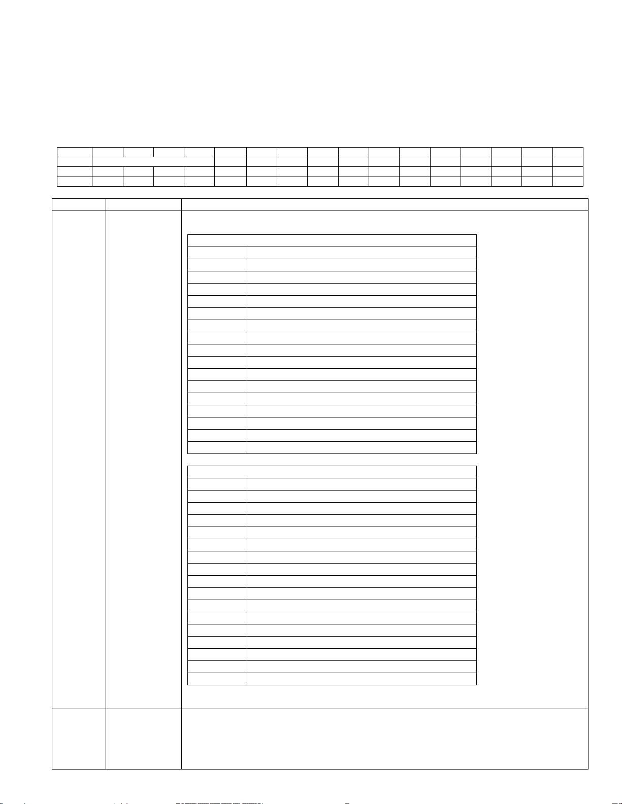
DS4830A User’s Guide
Bit
15
14
13
12
11
10 9 8 7 6 5 4 3 2 1 0
Name
SSC[3:0]
FAST_MODE
PIN_DIS1
PIN_DIS0
SH_DUAL
-
SH1_ALIGN
SHDAI1_EN
SMP_HLD1
CLK_SEL
SH0_ALIGN
SHDAI0_EN
SMP_HLD0
Reset
0 0 0 0 0 0 0 0 0 0 0 0 0 0 0
0
Access
rw
rw
rw
rw
rw
rw
rw
rw r rw
rw
rw
rw
rw
rw
rw
BIT
NAME
DESCRIPTION
15:12
SSC[3:0]
STOP Sample Control. These bits control the end of the sample and hold sampling
CLK_SEL = 0
SSC[3:0]
STOP Sampling
0000
Falling Edge of SHEN0/SHEN1
0001
Reserved
0010
Reserved
0011
Reserved
0100
300ns after rising edge of SHEN0/SHEN1
0101
350ns after rising edge of SHEN0/SHEN1
0110
450ns after rising edge of SHEN0/SHEN1
0111
550ns after rising edge of SHEN0/SHEN1
1000
750ns after rising edge of SHEN0/SHEN1
1001
1us after rising edge of SHEN0/SHEN1
1010
1.5us after rising edge of SHEN0/SHEN1
1011
1.75us after rising edge of SHEN0/SHEN1
1100
2us after rising edge of SHEN0/SHEN1
1101
2.5us after rising edge of SHEN0/SHEN1
1110
4us after rising edge of SHEN0/SHEN1
1111
5us after rising edge of SHEN0/SHEN1
CLK_SEL = 1
SSC[3:0]
STOP Sampling
0000
Falling Edge of SHEN0/SHEN1
0001
21 ext-clock after rising edge of SHEN0/SHEN1
0010
22 ext-clock after rising edge of SHEN0/SHEN1
0011
23 ext-clock after rising edge of SHEN0/SHEN1
0100
24 ext-clock after rising edge of SHEN0/SHEN1
0101
25 ext-clock after rising edge of SHEN0/SHEN1
0110
26 ext-clock after rising edge of SHEN0/SHEN1
0111
27 ext-clock after rising edge of SHEN0/SHEN1
1000
28 ext-clock after rising edge of SHEN0/SHEN1
1001
29 ext-clock after rising edge of SHEN0/SHEN1
1010
30 ext-clock after rising edge of SHEN0/SHEN1
1011
31 ext-clock after rising edge of SHEN0/SHEN1
1100
32 ext-clock after rising edge of SHEN0/SHEN1
1101
33 ext-clock after rising edge of SHEN0/SHEN1
1110
34 ext-clock after rising edge of SHEN0/SHEN1
1111
35 ext-clock after rising edge of SHEN0/SHEN1
used to guarantee accurate results.
11
FAST_MODE
Fast Mode Enable. Setting this bit to ‘1’ enables the fast operation for Sample and Hold
voltage channels in the sequence and the voltage conversions will be delayed. When
8.2 – Sample and Hold Register Descriptions
The sample and hold has two SFRs. These are Sample and Hold Control Register (SHCN) and Sample and Hold
Internal Trigger Enable register (SENR). The SHCN register controls both sample and holds. The SENR controls
the internal sample pulse for both sample and holds. The sample and hold SFRs are located in module 4.
8.2.1 – Sample and Hold Control Register (SHCN)
relative to the SHEN0 and SHEN1 pulse.
Note: A minimum sample time of 300nSec must be used when external clock is
0. In this mode, Sample and Hold 0 is guaranteed to get a conversion slot in the ADC
conversion sequence every 125µs and the user can issue sample pulses at an interval
of 125µs. During fast mode, the sample and hold conversion priority is increased over
70
Page 71

this bit is ‘0’, Sample and Hold 0 acts in the normal mode in which Sample and Hold 0
gets a conversion slot in the ADC sequence every 250µs.
10
PIN_DIS1
Pin Discharge Enable 1. Setting this bit to ‘1’ enables the pin discharge function for
after the Sample and Hold 1 ADC conversion.
9
PIN_DIS0
Pin Discharge Enable 0. Setting this bit to ‘1’ enables pin discharge function at Sample
Sample and Hold 0 ADC conversion.
8
SH_DUAL
Sample and Hold Dual Mode. Setting this bit to ‘1’ configures in “Dual Mode” Sample
triggered by the SHEN0 signal.
7 - Reserved. The user should write 0 to this bit.
6
SH1_ALGN
Sample and Hold 1 Data Alignment Select. This bit selects the Sample and Hold 1
:0] zero padded. Clearing this bit to ‘0’ returns data in right aligned
format in ADDATA[13:0] with ADDATA[15:14] sign-extended by ADDATA[13].
5
SHDAI1_EN
Sample and Hold 1 Interrupt Enable. Setting this bit to ‘1’ enables interrupt generation
on the completion of Sample and Hold 1 ADC conversion in the dual mode.
4
SMP_HLD1
Sample and Hold 1 Enable. Setting this bit to ‘1’ enables Sample and Hold 1 operation
on results are available in ADC data buffer
location 24.
3
CLK_SEL
Clock Select for Sample and Holds Trigger delayed rising edge control. This bit
When this bit is set to ‘0’, the peripheral clock is used for generating the SHEN pulse.
When this bit is set to ‘1’, the External Clock (CLKIN pin) is used for generating the
pulse generation.
2
SH0_ALGN
Sample and Hold 0 Data Alignment Select. This bit selects the Sample and Hold 0
:0] zero padded. Clearing this bit to ‘0’ returns data in right aligned
format in ADDATA[13:0] with ADDATA[15:14] sign-extended by ADDATA[13].
1
SHDAI0_EN
Sample and Hold 0 Interrupt Enable. Setting this bit to ‘1’ enables interrupt generation
and hold conversions.
0
SMP_HLD0
Sample and Hold 0 Enable. Setting this bit to ‘1’ enables Sample and Hold 0 operation
GP3 input pins. The conversion results are available in ADC data buffer
location 23.
Sample and Hold 1. The discharge function discharges pin capacitances (GP12-GP13)
and Hold 0. The discharge function discharges pin capacitances (GP2-GP3) after the
and Hold operation. In dual mode, both sample and holds act independently and use
different sample trigger input signals. SHEN0 (pin 23) acts as the sample trigger input
signal for Sample and Hold 0. SHEN1 (pin 21) acts as the sample trigger input signal
for Sample and Hold 1. In single mode operation both sample and hold circuits are
data alignment mode. Setting this bit to ‘1’ returns data left aligned in ADDATA[15:2]
with ADDATA[1
on GP12-GP13 input pins. The conversi
DS4830A User’s Guide
selects the clock used to stop sampling when operating in SSC mode. During this mode
SSC[3:0] bits controls the delay from the start to stop of sampling..
SHEN pulse.
See the SSC[3:0] bit description to see the effect of CLK_SEL on the SHEN0/SHEN1
data alignment mode. Setting this bit to ‘1’ returns data left aligned in ADDATA[15:2]
with ADDATA[1
on the completion of Sample and Hold 0 ADC conversion when operating in dual mode
operation. In the single mode operation, this bit is set at the completion of both sample
on GP2-
71
Page 72

Bit
15
14
13
12
11
10 9 8 7 6 5 4 3 2 1 0
Name
INT_TRIG_EN1
INT_TRIG1 - -
INT_TRIG_EN0
INT_TRIG0
Reset
0 0 0 0 0 0 0 0 0 0 0 0 0 0 0
0
Access
r r r r r r r r r r rw
rw r r
rw
rw
BIT
NAME
DESCRIPTION
15:6
-
Reserved. The user should write 0 to these bits.
5
INT_TRIG_EN1
Sample and Hold 1 Internal Trigger Enable. Setting this bit to ‘1’ enables internal
trigger mode for Sample and Hold 1. When this bit is set to ‘1’, writing a ‘1’ to
This bit is used in the dual mode operation only.
4
INT_TRIG1
Sample and Hold 1 Internal Trigger. This bit is used when INT_TRIG_EN1 is set to
operation only.
3:2 - Reserved. The user should write 0 to these bits.
1
INT_TRIG_EN0
Sample and Hold Internal Trigger Enable. Setting this bit to ‘1’ enables internal
trigger mode for Sample and Hold 0. When this bit is set to ‘1’, writing a ‘1’ to
In the single mode operation, this bit is used for both sample and holds.
0
INT_TRIG0
Sample and Hold0 Internal Trigger. This bit is used when the INT_TRIG_EN0 is set
bit is used for both sample and holds.
8.2.2 – Sample and Hold Internal Trigger Enable Register (SENR)
INT_TRIG1 starts an internal sample pulse for Sample and Hold 1. When this bit is
‘1’, sample pulses on SHEN1 are igonred.
Setting this bit to ‘0’ configures Sample and Hold 1 for external sample pulse.
‘1’. Setting this bit to ‘1’ starts internal sample pulse for Sample and Hold 1. The
sample pulse will end when this bit is set back to 0 if SSC[3:0] = 0, or after the time
defined by SSC[3:0] if these bits are not equal to 0. This bit is used in the dual mode
INT_TRIG0 starts an internal sample pulse for Sample and Hold 0. When this bit is
‘1’, sample pulses on SHEN0 are igonred.
Setting this bit to ‘0’ configures Sample and Hold 0 for ex ternal sample pulse.
DS4830A User’s Guide
to ‘1’. Setting this bit to ‘1’ starts internal sample pulse for Sample and Hold 0. The
sample pulse will end when this bit is set back to 0 if SSC[3:0] = 0, or after the time
defined by SSC[3:0] if these bits are not equal to 0.In the single mode operation, this
8.2.3 – Sample and Hold Interrupt flag
See ADST1 description for Sample and Hold interrupts fl ags SH0DAI and SH1DAI descriptions.
8.2.4 – Sample and Hold Averaging
See REFAVG description in ADC section for sample and hol d averaging options.
72
Page 73

DS4830A User’s Guide
QT CONFIGURATIONS
ADC-S0
ADC
-S1
ADC-S14
ADC-S15
A
N
A
L
O
G
M
U
X
QT SEQUENCER
QTSTART
QTEND
QTEN
QT HIGH
THRESHOLD
QT LOW
THRESHOLD
CHSEL[3:0]DIFF
Digital MUX
10-Bit
Internal
DAC
HT Register[0]
HT Register[14]
HT Register
[1
]
HT Register[15]
16
High Threshold
Registers
LT Register[0]
LT Register[14]
LT Register[1
]
LT Register[15]
16 Low Threshold
Registers
LIST REGISTER[0
]
LIST REGISTER[14]
LIST REGISTER[1]
LIST REGISTER[15]
16 List Configurations
5 bit Each
LTI / HTI
LTIE /
HTIE
Interrupt
QT CLOCK
QTDATA
[15:
0]
Comparator
QT- 2.42V
Internal
Reference
.
.
.
RW_LST = 0
LTHT = 0
RW_
LST = 1
.
.
.
.
.
.
RW
_
LST = 0
LTHT = 1
SECTION 9 – QUICK TRIP (FAST COMPARATOR)
The DS4830A has 10-bit quick trips with a 16-input analog MUX (Figure 9-1). The MUX selects the quick trip analog
input from 16 external channels. The quick tri p external channels can be configured to operate as eig ht fully
differential inputs or sixteen single-ended input s. The quick trip monitors all configured quick trip cha nnels in a round
robin sequence.
Figure 9-1: Quick Trip Functional Diagram
9.1 – Detailed Description
As shown in Figure 9-1, the DS4830A Quick Trip (QT) controller has a 16-input analog MUX and Quick Trip
Sequencer. The QT sequencer creates a list of configurations and sets user defined low and high threshold for
external channels. The quick trip controller has 16 low trip threshold and 16 high trip threshold internal registers.
The Quick Trip Control Register (QTCN) has two bits RW_LST and LTHT which are used to configure thresholds
and list creation. The QTIDX[3:0] bits (located in the QTCN register) together with LTHT and RW_LST bits select the
source or destination address for the QTDATA register access. Figure 9-1 illustrates the threshold configuration and
list creation.
73
Page 74

DS4830A User’s Guide
RW_LST
LTHT
QTIDX
REGISTER SELECTED
0
0
N(0 to 15)
Low threshold configuration for the channel defined in list N
0
1
N(0 to 15)
High threshold configuration for the channel define d in list N
1
X
N(0 to 15)
Nth register of list configuration
By default, the external channels GP0-15 are general-purpose input. The DS4830A has the Pin Select Register
(PINSEL). The PINSEL register is used to configure the external channels as an analog pin for ADC or/and Quick
Trip use. Each bit location in this register corresponds to the ADC/Quick Trip input pin.
Table 9-1: Low and High Thresholds Configuration and List Creation
Thresholds Configuration
Each configuration has two threshold registers to configure low and high threshold. Each threshold register is
addressed by the QTIDX[3:0] bits. These bits are auto incremented on any read or write operation to the QTDATA
register. The low trip thresholds are configured by writing to the QTDATA register when the RW_LST and LTHT bits
are set to ‘0’. The high trip thresholds are configured by writing to the QTDATA register when the RW_LST bit is set
to ‘0’ and LTHT bit is set to ‘1’.
List Creation
As shown in Figure 9-1, the quick trip controller has 16 list registers. These are configure d by writ ing to the Q TDATA
register when the RW_LST bit is set to ‘1’. The list address is addressed by the QTIDX[3:0] bits. Each list register
uses only lower 5 bits. The first 4 lower bits CHSEL [3:0] specifies the quick trip input channel. The DIFF bit selects
between single-ended mode (when DIFF bit is set to ‘0’) and differential mode (when DIFF bit is set to ‘1’) quick trip
comparison. The start and stop addresses of the list are provided by the Quick Trip List Register (QTLST). Any
channel can be used multiple times at any location in the list.
See Section 9.2 - Quick Trip Register Descripti ons for details.
As shown in Figure 9-1, the quick trip sequencer selects a channel from 16 external channels. The quick trip
controller has an internal 10-bit DAC which generates voltage for low and high threshold comparisons with the
external channel input. The quick trip is also called a “Fast Comparator” as it compares the input with threshold using
the fast comparator. The conversion time is 1.6µs for each threshold; so each channel’s thresholds are compared in
3.2µs (1.6µs for low trip threshold + 1.6µs for high trip threshold).
9.1.1 – Quick Trip List Sequencing
The DS4830A quick trip controller performs the user defined sequence of up to 16 single-ended or 8 differential
external channels conversions.
A sequence is setup in the QTLST register by defining the starting conversion configuration address (QTSTART) and
an ending conversion configuration address (QTEND). The configuration start address designates the configuration
register to be used for the first conversion in a sequence. The configuration end address designates the
configuration register used for the last conversion in a sequence. A single channel conversion can be viewed as a
special case for sequence conversion, where the starting and ending configuration address is the same. The
configuration registers can be viewed as a circular register array where QTSTART does not have to be less than
QTEND. For example, if QTSTART = 1 and QTEND = 5, then the sequence of conversions would be configurations
1, 2, 3, 4, 5. If QTSTART = 5 and QTEND = 1, then the sequence of conversions would be configurations 5, 6, 7 . . .
15, 0, 1.
9.1.2 – Operation
The quick trip is enabled by setting the Quick Trip Enable (QTEN) bit to ‘1’ in the QTCN register. The Quick Trip
Controller takes ~120 core clocks to wake up after enable and then starts scanning through the list of channels
specified in the channel list register QTLST continuously in the round robin sequence. The quick trip sequence reads
the list, selects the input channel and reads the low trip threshold and performs 10-bit comparison, then reads the
high trip threshold and again performs 10-bit comparison. The quick trip has separate interrupt flag registers for the
low and high trip threshold. The low trip interrupt flag is set when the input voltage is less than the configured low
threshold. Similarly, the high trip interrupt flag is set when the input voltage is greater than the configured high
threshold. The interrupt can be generated if enabled.
The channel list can be filled up using the QTDATA register by setting the RW_LST bit to ‘1’ in the QTCN register.
For example to scan channels S5, S6 and S14-15 having configurations for channels 5 & 6 in the single-ended
mode, channel 7 (S14-S15) in the differential mode and channel 6 again (any channel can be configured multiple
74
Page 75

DS4830A User’s Guide
Channel 5
LT HT
Channel 6
LT
HT
Channel 7
LT HT
……….
Channel 5
LT HT
Channel 6
LT HT
Channel 7
LT HT
……….
Channel 6*
LT HT
Channel 6*
LT HT
* Note: Channels can be defined multiple times in the list.
QT LIST
NUMBER
LIST REGISTERS USED FOR
COMPARISON
0
05h
Channel 5 (S5) in single-ended mode
LT0 and HT0
1
06h
Channel 6 (S6) in single-ended mode
LT1 and HT1
2
17h
Channel 7(S14-S15) in differential mode
LT2 and HT2
3
06h
Channel 6 (S6) in single-ended mode
LT3 and HT3
QT LIST NUMBER
LOW THRESHOLD VALUE (AS EXAMPLE)
QTDATA
0
0.6V
0x00FE
1
0.8V
0x0153
2
1.0V
0x01A7
3
1.1V
0x01D1
times in the QT list). The quick trip list can be filled sequentially with data 05h (channel 5 + single-ended), 06h
(channel 6 + single-ended), 17h (channel 7 + differential mode) and 06h (channel 6 + single-ended). See Table 9-2
for the quick trip list configurations.
To scan thes e list registers shown in Table 9-2, the QTSTART bits are set to 0 (0000b) and the QTSTOP bits are
set to 3 (0011b). Each channel is compared twice ( see Figure 9-2). First the low tr ip threshold (LT) is compared and
then the high trip threshold (HT). The sequence of comparisions is shown is Figure 9-2.
Table 9-2: Quick Trip List Configuration
QTDATA DESCRIPTION
Quick Trip Start address (QTSTART) = 0
Quick Trip Stop address (QTEND) = 3
Figure 9-2: Quick Trip Operation
9.1.3 – Setting Quick Trip Thresholds
The quick trip threshold can be calculated by using the following formula.
Table 9-3 demonstrates Quick Trip low and high threshold configuration.
Table 9-3: Quick Trip Low Threshold Configuration
QTCN = 0x0000; //Low Threshold Configuration Register, Index = 0
QTDATA = 0x00FE; //0.6V Low Threshold Configuration for List0 Configuration
QTDATA = 0x0153; //0.8V Low Threshold Configuration for List1 Configuration
QTDATA = 0x01A7; //1.0V Low Threshold Configuration for List2 Configuration
QTDATA = 0x01D1; //1.1V Low Threshold Configuration for List3 Configuration
75
Page 76

DS4830A User’s Guide
QT LIST NUMBER
HIGH THRESHOLD VALUE (AS EXAMPLE)
QTDATA
0
2.2V
0x03A3
1
2.0V
0x034E
2
1.8V
0x02FA
3
1.6V
0x02A5
Table 9-4: Quick Trip High Threshold Configuration
QTCN = 0x0010; //High Threshold Configuration Register, Index = 0
QTDATA = 0x03A3; //2.2V High Threshold Configuration for List0 Configurati on
QTDATA = 0x034E; //2.0V High Threshold Configuration for List1 Configuration
QTDATA = 0x02FA; //1.8V High Threshold Configuration for List2 Configuration
QTDATA = 0x02A5; //1.6V High Threshold Configuration for List3 Configuration
9.1.4 – Quick Trip Interrupts
The DS4830A quick trip has four interrupt flag registers the Low Trip Interrupt Lower Flag Register (LTIL), High Trip
interrupt Lower Flag Register (HTIL), Low Trip Interrupt High Register and High Trip Interrupt High Register. See the
register descriptions for the quick trip interrupt operation.
76
Page 77

DS4830A User’s Guide
Bit
15
14
13
12
11
10 9 8 7 6 5 4 3 2 1 0
Name - - - QTEN - - - -
RW_LST
- - LTHT
QTIDX[3:0]
Reset 0 0 0 0 0 0 0 0 0 0 0 0 0 0 0 0
Access r r r rw r r r r
rw r r
rw
rw
rw
rw
rw
BIT
NAME
DESCRIPTION
15:13
-
Reserved. The user should write these bits to ‘0’.
12
QTEN
Quick Trip Enable. When this bit is set to ‘1’, it enables the quick trip operation. After
setting the QTEN bit to ‘1’, there is an initial delay for 120 core clock to wake up the
11:8
-
Reserved. The user should write these bits to ‘0’.
7
RW_LST
Read List Register: When this bit is set to ‘1’, it selects one of the sixteen list register
the low or high threshold register (depends up on the LTHT bit) are configured.
6:5 - Reserved. The user should write these bits to ‘0’.
4
LTHT
Low or High Threshold Select: This bit is used only when RW_LST is set to ‘0’. This
the high threshold configuration register list. The address of low or high threshold
configuration is addressed by QTIDX[3:0] bi ts.
3:0
QTIDX[3:0]
Quick Trip Index Select. These bits together with LTHT and RW_LST bits select the
register addressed by QTIDX[3:0] bits for read and write operation. A read or write
to the list register addressed by
These bits are auto incremented on any read or write operation to the QTDATA register.
9.2 – Quick Trip Register Descriptions
The quick trip has 7 SFRs. These are the Quick Trip Control Register (QTCN), Quick Trip List Register (QTLST),
Quick Trip Data Register (QTDATA), Low Trip Interrupt Lower Flag Register (LTIL), High Trip Interrupt Lower Flag
Register (HTIL), Low Trip Interrupt High Register (LTIH) and High Trip Interrupt High Register (HTIH). The QTC N
register controls the quick trip operation. The QTLIST register defines the list for the quick trip controller. The
QTDATA register is used to read and write list and threshold (high and low threshold) registers. The LTIL and HTIL
are interrupt flag registers for high and low threshold. The LTIH and HTIH are the interrupt enable registers. The
Quick Trip SFRs are located in module 5.
9.2.1 – Quick Trip Control Register (QTCN)
quick trip circuitry. When this bit is set to ‘0’, it disables the quick trip operation.
(addressed by QTIDX[3:0], see below) in the list configuration. When this bit is set to ‘0’,
bit is used to select l ow or high threshold read or write. When the LTHT bit is set to ‘0’, it
points to the low threshold configuration register list. When this bit is set to ‘1’, it points to
source or destination address for the QTDATA register access.
When the RW_LST and LTHT bits are set to ‘0’, the QTIDX[3:0] bits address to one of
the sixteen low threshold register for read or write. When RW_LST = 0 and LTHT = 1,
the QTIDX[3:0] bits address one of the sixteen high threshold register for read or write.
When RW_LST = 1 (irrespective of LTHT bit), the QTDATA register selects the list
operation on the QTDATA register reads or writes
QTIDX[3:0].
9.2.2 Quick Trip Data Register (QTDATA)
The Quick Trip Data register is used with LTHT, RW_LST and QTIDX[3:0] bits to configure thresholds and list
configurations. The QTDATA register selects the list register and threshold registers addressed by QTIDX[3:0] bits
for read and write operation.
Threshold registers are selected when the bit RW_LST is set to ‘0’. List registers are selected when the bit RW_LST
is set to ‘1’. See the following tables for RW_LST = 0 and RW_LST = 1.
77
Page 78

Bit
15
14
13
12
11
10 9 8 7 6 5 4 3 2 1 0
Name
-
LOW or HIGH THRESHOLD
Reset 0 0 0 0 0 0 0 0 0 0 0 0 0 0 0 0
Access r r r r r r
rw
rw
rw
rw
rw
rw
rw
rw
rw
rw
BIT
NAME
DESCRIPTION
15:10
-
Reserved. The user should write these bits to ‘0’.
9:0
QTDATA[9:0]
a. Low Threshold Configuration (When the LTHT bit in the QTCN register is set to ‘0’)
The QTDATA selects high threshold register addressed by QTIDX[3:0] bits in the
wide and upper QTDATA [15:10] bits are ignored and return 0.
Bit
15
14
13
12
11
10 9 8 7 6 5 4 3 2 1 0
Name - - - - - - - - - - - DIFF
CHSEL[3:0]
Reset 0 0 0 0 0 0 0 0 0 0 0 0 0 0 0 0
Access r r r r r r r r r r r rw
rw
rw
rw
rw
BIT
NAME
DESCRIPTION
15:5
-
Reserved. The user should write these bits to ‘0’.
4
DIFF
Mode Selection (DIFF): This bit selects the Quick trip input channel source either as
or differential mode. When this bit is set to ‘0’, quick trip channel
ended as well as differential mode.
3:0
CHSEL [3:0]
QT Channel Select (CHSEL [3:0]): These bits select the Quick trip input channel
CHSEL[3:0]
DIFF = 0
Single-Ended
DIFF = 1
Differential Mode
0000
ADC-S0
ADC-D0P – ADC-D0N
0001
ADC-S1
ADC-D1P – ADC-D1N
0010
ADC-S2
ADC-D2P – ADC-D2N
0011
ADC-S3
ADC-D3P – ADC-D3N
0100
ADC-S4
ADC-D4P – ADC-D4N
0101
ADC-S5
ADC-D5P – ADC-D5N
0110
ADC-S6
ADC-D6P – ADC-D6N
0111
ADC-S7
ADC-D7P – ADC-D7N
1000
ADC-S8
NOT VALID
1001
ADC-S9
NOT VALID
1010
ADC-S10
NOT VALID
1011
ADC-S11
NOT VALID
1100
ADC-S12
NOT VALID
1101
ADC-S13
NOT VALID
1110
ADC-S14
NOT VALID
1111
ADC-S15
NOT VALID
QTDATA Register map when RW_LST = 0 (in the QTCN Register)
The QTDATA register selects low threshold register addressed by QTIDX[3:0] bits in
the QTCN register for read and write operation. The low threshold registers are 10-bit
wide and the upper QTDATA [15:10] bits are ignored and return 0.
b. High Threshold Configuration (When the LTHT bit in the QTCN register is set to ‘1’)
QTCN register for read and write operation. The high threshold registers are 10-bit
QTDATA Register map when RW_LST = 1 (in the QTCN Register)
DS4830A User’s Guide
single-ended
(addressed by CHSEL[3:0]) is selected as “single-ended” input. When this bit is set to
‘1’, quick trip channel (addressed by CHSEL[3:0]) is selected as “Differential Mode”
input. See the below table for various quick trip input channel configuration in single-
source for the quick trip list configuration.
Channel Selected
Channel Selected
78
Page 79

Bit
15
14
13
12
11
10 9 8 7 6 5 4 3 2 1 0
Name
IE[7:0]
IF[7:0]
Reset
Access
rw
rw
rw
rw
rw
rw
rw
rw
rw
rw
rw
rw
rw
rw
rw
rw
BIT
NAME
DESCRIPTION
15:8
IE[7:0]
Low Trip Interrupt Enable. This register is used to enable/mask the corresponding
= 0x0100 then Quick Trip list 0 can
7:0
IF[7:0]
Low Trip Interrupt Flag. The corresponding bit of the Low Trip Interrupt register is set
Bit
15
14
13
12
11
10 9 8 7 6 5 4 3 2 1 0
Name
IE[7:0]
IF[7:0]
Reset
Access
rw
rw
rw
rw
rw
rw
rw
rw
rw
rw
rw
rw
rw
rw
rw
rw
BIT
NAME
DESCRIPTION
15:8
IE[7:0]
High Trip Interrupt Enable. This register is used to enable/mask the corresponding
= 0x0100 then Quick Trip list 0 can
7:0
IF[7:0]
High Trip Interrupt Flag. The corresponding bit of the High Trip Interrupt register is
when voltage across channel is greater than the high threshold configuration for the
should clear the how trip interrupt flag once it is set by hardware. Setting this bit to ‘1’
by software generates an interrupt if enabled.
9.2.3 Low Trip Interrupt Lower Register (LTIL)
LTIL register interrupts. For Example, if LTIL
generate an interrupt when LTIL LSB is set to ‘1’ and all other interrupts from LTIL are
ignored. Similarly, if LTIL = 0xFF00, then all 8 interrupts from LTIL generate interrupts.
when a low threshold trip is occurred on a channel list register. In other words, when
voltage across channel is less than the low threshold configuration for the channel.
For example, if a low trip occurs on the list register 0 then LTIL is set to 0x0001. If the
corresponding IE bit is also ‘1’, and then this generates an interrupt. Software should
clear the Low Trip Interrupt Flag once it is set by hardware. Setting this bit to ‘1’ by
software generates an interrupt if enabled.
9.2.4 High Trip Interrupt Lower Register (HTIL)
DS4830A User’s Guide
HTIL register interrupts. For example, if HTIL
generate an interrupt when HTIL LSB is set to ‘1’ and all other interrupts from HTIL are
ignored. Similarly, if HTIL = 0xFF00, then all 8 flags from HTIL generate interrupts.
set when a high threshold trip is occurred on a channel list register. In other words,
channel.
For example, if a high trip occurs on the list register 0 then HTIL is be set to 0x0001. If
the corresponding IE bit is also ‘1’, and then this generates an interrupt. Software
79
Page 80

Bit
15
14
13
12
11
10 9 8 7 6 5 4 3 2 1 0
Name
IE[15:8]
IF[15:8]
Reset
Access
rw
rw
rw
rw
rw
rw
rw
rw
rw
rw
rw
rw
rw
rw
rw
rw
BIT
NAME
DESCRIPTION
15:8
IE[15:8]
Low Trip Interrupt Enable. This register is used to enable/mask the corresponding
generate interrupts.
7:0
IF[15:8]
Low Trip Interrupt Flag. The corresponding bit of the low trip interrupt register is set
clear the Low Trip Interrupt Flag once it is set by hardware. Setting this bit to ‘1’ by
Bit
15
14
13
12
11
10 9 8 7 6 5 4 3 2 1 0
Name
IE[15:8]
IF[15:8]
Reset
Access
rw
rw
rw
rw
rw
rw
rw
rw
rw
rw
rw
rw
rw
rw
rw
rw
BIT
NAME
DESCRIPTION
15:8
IE[15:8]
High Trip Interrupt Enable. This register is used to enable/mask the corresponding
from HTIH generate interrupts.
7:0
IF[15:8]
High Trip Interrupt Flag. The corresponding bit of the High Trip Interrupt register is
threshold trip is occurred on a channel list register. In other words,
threshold configuration for the
‘1’ by software generates an interrupt if enable d.
Bit
15
14
13
12
11
10 9 8 7 6 5 4 3 2 1 0
Name - - - -
QTSTART[3:0]
- - - - QTEND[3:0]
Reset 0 0 0 0 0 0 0 0 0 0 0 0 0 0 0 0
Access r r r r
rw
rw
rw
rw r r r r
rw
rw
rw
rw
BIT
NAME
DESCRIPTION
15:12
-
Reserved. The user should write these bits to ‘0’.
11:8
QTSTART[3:0]
Quick Trip Configuration Start Address Bits [3:0]. These bits select the start
7:4 - Reserved. The user should write these bits to ‘0’.
3:0
QTEND[3:0]
Quick Trip Configuration Ending Address Bits [3:0]. These bits select the stop
address of quick trip channel list.
9.2.5 Low Trip Interrupt High Register (LTIH)
LTIH register interrupts for upper 8 comparisions. For example, if LTIH = 0x0100 then
Quick Trip list 8 can generate an interrupt when LTIH LSB is set to ‘1’ and all other
interrupts from LTIH are ignored. Similarly, if LTIH = 0xFF00, then all 8 flags from LTIH
when a low threshold trip is occurred on a channel list register. In other words, when
voltage across channel is less than the low t hreshold configuration for the channel.
For example, if a low trip occurs on the list register 8 then LTHI is set to 0x0001. If the
corresponding IE bit is also ‘1’, and then this generates an interrupt. Software should
software generates an interrupt if enabled.
9.2.6 High Trip Interrupt High Register (HTIH)
DS4830A User’s Guide
HTIH register interrupts for the upper 8 comparisons. For Example, if HTIH = 0x0100
then Quick Trip list 8 can generate an interrupt when HTIH LSB is set to ‘1’ and all
other interrupts from HTIH are ignored. Similarly, if HTIH = 0xFF00, then all 8 flags
set when a high
when voltage across channel is more than the high
channel.
For example, if a high trip occurs on the list register 8 then HTIH is set to 0x0001. If
the corresponding IE bit is also ‘1’, and then this generates an interrupt. Software
should clear the High Trip Interrupt Flag once it is set by hardware. Setting this bit to
9.2.7 – Quick Trip List Register (QTLST)
address of quick trip channel list.
80
Page 81

DS4830A User’s Guide
SECTION 10 – I2C-COMPATIBLE MASTER INTERFACE
The DS4830A provides an I
device. The I
2
C master interface can be setup to provide system i nterrupts after each I2C event.
10.1 – Detailed Description
10.1.1 – Description of Master I2C Interface
The master I
the SDA and SCL pins of an I
both MSDA and MSCL. This allows the I
stretch.
Unless explicitly stated, all references to SDA and S CL in this section refer to the SDA and SCL lines of the I
not the DS4830A’s I
10.1.2 – Default Operation
2
The I
I2CMST bits in the I2CCN_M register to a 1. Prior to the I
software setup is required. This setup includes setting the clock rate, timeout period, and which I
generate interrupts. The DS4830A master I
masters connected to the bus.
10.1.3 – I
In an I
provides complete control over the clock rate and duty cycle. The I
system clock. The bit rate is controlled by the I
The high period of SCL clock is defined by the high byte of the I
the low period of SCL is defined by the low byte (I2CCKL). The minimum clock high period is three system clocks
while the minimum low period has to be at least five system clock periods. The I
defined by the following equations:
• SCL Low Time = System Clock Period x (I2CCKL[ 7:0] + 1)
• SCL High Time = System Clock Period x (I2CCKH[7:0] + 1)
• I
One feature of the master I
controller to ensure that the SCL level is at the desired level prior to beginning the count for SCL Low or High Time.
Figure 10-1 illustrates the SCL sampling performed by the master I
master I
When the controller senses the SCL line has reached a high logic level, the count for SCL High Time is started. The
same is true for a falling edge. The SCL Low Time is only started after the controller senses the SCL line at a low
logic level.
Figure 10-1 also illustrates that the calculated I
of SCL is not taken into consideration. The actual clock period will be the period set by the I2CCK_M register plus
any rise and fall time.
2
C interface uses the MS DA and MSCL pins. These pins are the master I2C controller’s connection to
2
C slave interface SDA and SCL pins.
C master controller is disabled by default. The I2C master controller is enabled by setting the I2CEN and
2
C Clock Generation
2
C system, the master is responsible for generating the SCL signal. The DS4830A I2C Master Controller
2
C Clock Rate = System Clock Frequency/(I2CCLK[7:0] + I2CCKH[7:0] + 2)
2
C controller, the rise time is determined by the capacitive loading and pullup resistance on the SCL line.
2
C-compatible master controller that allows the DS4830A to communicate with a slave
2
C bus. In addition to driving these pins, the I2C master port also senses the state of
2
C controller is that it also monitors SCL while the clock is being output. This allows the
2
C master port to offer bus error detection and allows a slave device to clock
2
C bus,
2
C master controller being used for communication, some
2
C controller is not intended to be used on an I2C bus that has multiple
2
2
C Clock Control Register (I2CCK_M).
2
C clock peri od is not exactly accurate because the rise and fall time
C Master Controller generates SCL from the
2
C Clock Control register (I2CCKH) whereas
2
C clock characteristics can be
2
C controller. When SCL is released by the
2
C events should
81
Page 82

DS4830A User’s Guide
Figure 10-1: I
2
C Clock Generation
The master I2C controller’s ability to monitor the state of SCL allows the master to operate with slave devices that
stretch the clock. A slave device may clock stretch, or hold SCL low, while it is busy or processing data. The master
2
C controller will always release SCL after holding it low for the SCL Low Time duration. By monitoring the state of
I
SCL, the master I
2
C controller realizes that SCL has not been released and does not begin the SCL High Time
count. Only after the master controller detects a high state on SCL will begin the I2CCKH count. This is illustrated in
Figure 10-2.
Figure 10-2: Master I
2
C Clock Generation During Slave Clock Stretching
10.1.4 – Timeout
The Master I
error. The timeout period is determined by the setting of the I
2
C Controller has a programmable timeout function that allows the controller to recover from a bus
2
C Master Timeout Register (I2CTO_M) using the
following equation:
2
where I
C Bit Rate is determined by the setting of the I2CCK_M register. The timeout can be disabled by clearing the
I2CTO_M register to 0. The I
• When the I2CSTART bit is set to 1. The I
START condition. The I
2
C timeout timer starts counting:
2
C bus is considered busy if another master has generated a START condition
and no corresponding STOP has been detected (the I2CBUS bit is set to 1) or the SCL line is low. If the
bus remains busy for a period longer than specified in the timeout register, the I
Timeout Period = I
2
C controller will monitor the bus status until it can generate a
2
C Bit Rate x (I2CTO[7:0]+1)
2
C controller concludes
that there is a bus error and will set the I2CTOI flag.
If the I
transfer to finish (after the 9
condition. In this case, the timeout timer will start counting after the end of the 9
• After the master I
2
C Controller has started a transfer (after the first bit rising edge), it will wait for the current byte
2
C controller attempts to generate a STOP condition. If a STOP is not detected (I2CSPI =
th
bit (acknowledge) has been transmit) before generating the START
th
bit low time.
1) during the timeout period, the I2CTOI flag will be set.
If the I2C Controller has started a transfer (after the first bit rising edge), it will wait for the current byte transfer to
finish (after the 9th bit (acknowledge) has been transmit) before generating the STOP condition. In this ca se,
the timeout timer will start counting after the end of the 9th bit low time.
• Whenever SCL goes low. If the SCL line is low for a period longer than specified in the timeout register, the
2
C controller concludes that there is a bus error and will set the I2CTOI flag.
I
82
Page 83

DS4830A User’s Guide
For all of these cases, when the I
generate an interrupt if enabled. If the master I
occurs, the controller will abort the current transfer and clear the I2CBUSY flag. The I2CBUS flag will continue to be set
until a STOP condition is detected or I2CEN is set to 0.
10.1.5 – Generating a START
To initiate a data transfer, the I
flow when attempting to issue a START command is shown in Figure 10-3. A START command is generated by
setting the I2CSTART bit to 1. The I
(I2CBUS = 1), the controller will not generate a START until the bus is available. The I
another master has generated a START condition and no corresponding STOP has been detected (the I2CBUS
bit is set to 1) or SCL is being held low.
If the bus is not busy, the I
feedback into the device, when the master generates a START, it can also detect the START condition. When a
START condition is detected, the I
enabled. The I2CBUS bit will be set to indicate that the I
cleared.
When the I2CSTART bit is set to a 1, the I
the timer expires before the START can be generated, the I
interrupt is generated if enabled. If a timeout occurs, the I
I2CSTART bit will be cleared.
If the I2CSTART bit is set when the I
the controller will wait for the current byte transfer to finish (after the 9th bit) before generating the START
condition. In this case, the timeout timer will not start counting until after the end of the 9th bit low time.
2
C timeout per iod is reached, the I2CTOI flag will be set. The setting of I2CTOI can
2
C master controller must firs t issue a START com mand . The m ast er I2C controller’s
2
C controller will then determine the state of the I2C bus. If the bus is busy
2
C master controller will attempt to generate a START. Because the SDA line is
2
C START interrupt flag (I2CSRI) will be set and an interrupt will be generated if
2
C Controller is in the middle of a byte transfer (after the first bit rising edge),
2
C controller is in the process of transferring data when the timeout
2
C bus is considered busy if
2
C bus is now in use and the I2CSTART bit will be
2
C controller will start its timeout timer if enabled (I2CTO_M ≠ 0). If
2
C timeout interrupt flag (I2CTOI) will be set and an
2
C master controller will reset to an idle state and the
83
Page 84

Timeout
?
I2CTOI=1
N
Y
N
Y
Generate
START
I2CSTART=1
I2CSTART=0
I2CBUSY=0
I2CBUSY=1
Repeated
Start
?
I2CBUS = 1
N
Y
START
Detected?
I2CSRI=1
I2CBUS=1
Timeout
?
N
Y
N
Y
Generate
STOP
I2CSPI=1
I2CBUS=0
I2CSTOP=1
I2CSTOP=0
I2CBUSY=0
I2CBUSY=1
STOP
Detected?
I2CTOI=1
Timeout
?
N
Y
N
Y
Transferring
Byte?
Y
N
Transfering
Byte
?
Y
N
START Generation STOP Generation
DS4830A User’s Guide
Figure 10-3: Master I2C-Generated START and STOP
84
Page 85

DS4830A User’s Guide
10.1.6 – Generating a STOP
To end an I
master I
If the I2CSTOP bit is set whe n th e I
wait for the current byte transfer to finish (after the 9
Because the SDA line is feedback into the device, when the master generates a STOP, it will also detect the
STOP condition. When a STOP condition is detected, the I
interrupt will be generated enabled. The I2CBUS bit will be cleared to indicate that the I
I2CSTOP bit will be cleared.
When the master I
feature is enabled. If a timeout is generated before the STOP condition is detected, a timeout will occur. When a
timeout occurs, the I2CTOI bit will be set, which can generate an interrupt if enabled, and the I2CSTOP bit will also
be cleared to 0.
10.1.7 – Transmitting a Slave Address The first byte after an I master, contains seven bits of slave address followed by the R/W bit. The transmission of the slav e address begins with writing 7-bit slave address + the R/W bit to I2CBUF_M.
Figure 10-4 shows the format for slave address 36h in write mode. The address bits A[6:0], which is the slave
address the R/W bit is written to I2CBUF_M[6:0]. Bit 0 of I2CBUF_M is copied to bit 0 I2CMODE of the I2CSLA_M
register. When bit 0 is ‘1’, the I
2
C master is operating in transmitter mode (data write to slave).
I
2
C transfer, a STOP must be transmit ted. A STOP is generated by setting the I2CSTOP bit. The
2
C controller’s flow when attempting to issue a STOP command is shown in Figure 10-3.
2
C Controller is in the m iddle of a byt e transfer (after the first bit rising edge), it will
2
C controller attempts to generate the STOP condition, it will also start the timeout timer if this
2
C START or restart condition is the slave address byte. This by te, which is transmitted by the
2
C master is operating in receiver mode (data read from slave). When bit 0 is ‘0’, the
th
bit) before generating the STOP condition.
2
C STOP interrupt flag (I2CSPI) will be set and an
2
C bus is now idle and the
Figure 10-4: Slave Address Format
After the slave address has been written to I2CBUF_M, the I
the controller is actively participating in a transaction. The eight bits in I2CBUF_M[7:0] will be transmitted on SDA.
The data for the 8
2
C master then issues the 9th clock, which is for the acknowledge bit, and reads SDA for an acknowledgment from a
I
slave device. The I
th
bit transmit, which is the R/W bit, is copied in the I2CMODE bit of the I2CSLA_M register. The
2
C master controller then performs the following st eps. This is illustrated in Figure 10-5.
2
C master controller will set the I2CBUSY bit to indicate
• Set the I2CNACKI bit with the value of the re ceived acknowledgement.
• The I2CTXI bit will then be set to indicate a byte was transmit.
• Clear the I2CBUSY flag.
Upon transmitting the slave data byte (7 bits of slave address + R/W bit + acknowledge), the I
2
C master controller
will enter one of the three states.
• Data Transmit: The I2CMODE (R/W) bit wa s set to a 0, indicating that the master will be writin g data to a
slave device. The DS4830A will retain control of the SDA line.
• Data Receive: The I2CMODE (R/W) bit was set to a 1, indicating that the master will be receiv i ng data from
a slave. The DS4830A releases control of S DA to allow a slave device to output data. The DS4830A
Master I
• The slave address was NACKed. The master I
2
C controller automatically begins clocking bytes of data from the slav e.
2
C controller will retain control of SDA and is able to transmit
data.
10.1.8 – Transmitting Data
The DS4830A I
2
C Master Controller enters into data transmission mode after transmitting a slave address with the
R/W bit (I2CMODE) set to a 0. The steps of data transmission are shown in Figure 10-5. Data transmis sion is
started by software loading a byte of data into the I2CBUF_M register. Loading I2CBUF_M causes the I2CBUSY bit
85
Page 86
DS4830A User’s Guide
I2CNACKI =
ACKNOWLEDGE
Transmit I2CBUF_M[7:0]
I2CBUF_M[0] I2CMODE
I2CBUSY=1
I2CTXI=1
I2CBUSY=0
Write to
I2CBUF_M
RECEIVE
ACKNOWLEDGE
Transmitting
Byte
Receiving
Byte
I2CNACKI =
ACKNOWLEDGE
Transmit Shift
Register Byte,
MSB First
N
Y
I2CBUSY=1
8 Bits
Transmit?
I2CTXI=1
I2CBUSY=0
Write to
I2CBUF_M
Receive a Bit into
Shift Register
MSB first
N
Y
I2CBUSY=1
8 Bits
Received?
Load Shift
Register into
I2CBUF_M
I2CRXI=1
Send
I2CACK
Y
N
I2CROI=1
Receiver
Full
?
First SCL
Rising Edge
Generated
I2CBUSY=0
RECEIVE
ACKNOWLEDGE
Transmitting
Slave Address
to be set. Once set, writes to I2CBUF_M will be ignored. The first bit of data (most significant bit ) wi ll be shifted to
SDA when SCL is low. Each of the next seven bits wi ll then be shifted following high to low transitions of SCL.
Following the 8
master controller. This allows the slave to signal an ACK or NACK during the 9
master controller samples the acknowledge bit following the 9
sampled, the DS4830A I
• Set or clear the I2CNACKI flag to reflect the received acknowledge bit. The setting of I2CNACKI can
generate an interrupt if enabled.
• Set the I2CTXI flag to indicate that the I
interrupt if enabled.
• Clear the I2CBUSY flag to indicate that the I
data.
th
bit of data (least significant bit) being shifted to SDA, the SDA line will be released by the DS4830A
th
2
C master controller will perform the following tasks:
2
C master controller transmit a complete byte. This can generate an
2
C master controller is not actively participating in the transfer of
SCL rising edge. After the acknowledge bit is
th
clock cycle. The DS4830A I2C
Figure 10-5: Master I2C Data Flow
86
Page 87

DS4830A User’s Guide
10.1.9 – Receiving Data
The DS4830A I
2
C Master Controller enters data reception mode after transmitting a slave address with the R/W bit
(I2CMODE) set to a 1. The steps of data reception are shown in Figure 10-5. After transmitting the slave address,
the master controller will switch to receiver mode and automatically begin outputting SCL clock pulses and shifting in
data from SDA.
When receiving data, the DS4830A I
and the shift register. This allows the I
processed. When a full byte of data (8 bits) has been received by the I
acknowledgement to the slave. This occurs during the 9
2
C master controller uses a double buffer consisting of the I2CBUF_M register
2
C module to continue receiving data while the previous data byte is being
th
clock cycle when the value in I2CACK is transmitted to the
2
C master controller, the master must send an
slave.
After a complete byte (8 bits) of data is received, the I
the shift register to I2CBUF_M. There are two possible results from the I
2
C master controller will attempt to copy the received data from
2
C master controller’s attempt to copy the
shift register to I2CBUF_M.
1. If I2CBUF _M is empty, the I
2
C master controller will copy the data from the shift register into I2CBUF_M.
The I2CRXI flag will be set to indicate a received byte is ready to be read. The setting of I2CRXI can
generate an interrupt if enabled.
2. If I2CBUF_ M is full, the data in the shift register cannot be copied into I2CBUF_M. This causes a receive
overrun condition. The receive overrun flag, I2CROI, will be set which can generate an interrupt if enabled.
I2CBUF_M will be full if it was not read by software following the reception of a previous byte.
After receiving a byte of data and the I2CRXI flag being set, it is up to software to read I2CBUF_M prior to a second
byte being received. Reading the I2CBUF_M register returns the received data and also clears I2CBUF_M. As long
as the previous byte of data is read from I2CBUF_M before the next byte has completed, receive overrun will not
occur.
When receive overrun is detected and I2CROI bit is set, the DS4830A master I
2
C controller will stop outputting SCL
clocks and not clock the acknowledge bit until the receive overrun condition is cleared. The receive overrun condition
and the I2CROI flag can only be cleared by software reading the first byte received from I2CBUF_M. When the
receive overrun condition is cleared, the I
I2CBUF_M, and again set I2CRXI to indicate a byte of data was received. The I
2
C master controller will copy the second byte that was received into
2
C master controller will resume
clocking SCL after satisfying SCL low time requi rements.
The master I
1) A receive overrun condition occurs.
2
C controller will continue to automatically clock bytes of data until any of the following condit i ons occur.
2) A STOP command is issued (I2CSTOP=1) prior to the master I2C controller beginning to clock a new byte.
3) The master I2C controller has clock stretching enabled and the clock is currently being held low by the
master.
87
Page 88

DS4830A User’s Guide
10.1.10 – I
The Master I
SCL is held low. If the I
after the clock pulse defined by the I
SCL low after the falling edge of the 9
falling edge of the 8
(I2CSTRI) will be set, which can generate an interrupt if enabl ed. The I
I2CSTRI is cleared to 0 by software.
If clock stretching is enabled after the 8
the I2CACK bit until clock stretching is released by clearing I2CSTRI. This allows software time t o examine the data
that was received prior to sending an ACK or NA CK to the slave. The continuous output of I2CACK will occur even if
the master I
allow the slave to send the proper acknowledgement, the I2CACK bit should be set to a 1, which pr om pts the master
2
I
C controller to release SDA.
The Master I
the master I
generation is only halted when a STOP command i s iss ued or a receive overrun occurs. If clock stretching is
enabled, software can control when each byte of data is clocked from the slave device.
10.1.11 – Resetting the I
The I
I2CCN_M register. A reset will force the master I
low by the I
reset the I
initialized before it can be used again.
After a reset, the master I
is recommended that the master I
A reset of slave devices can be performed by outputting at least 9 clock pulses on the MSCL line while MSDA is
high. This easiest way to achieve this is to use MSDA and MSCL as GPIO pins (see the GPIO section) while the
master I
can be done either using GPIO, or by enabling the m ast er I
2
C Master Clock Stretching
2
C Controller is capable of clock stretching at the end of each transfer cycle. Clock stretching is when
2
C controller is transmitting data. In this mode, the slave should be sending the acknowledgement. To
2
C Controller may need to use clock stretching when receiving data from a slave. When receiving data,
2
C controller automatically generates clock pulses. Without using clock stretching, this aut omatic clock
2
C master controller can be reset by disabling the I2C master controller by writing ‘0’ at I2CEN = 0 in the I2CCN
2
C master controller. A reset may reset few or all bits of I2CCN, I2CST and I2CBUF I2C registers, and
2
C master controller’s internal state machine. Following a reset, the I2C master controller must be re-
2
C controller is disabled (I2CEN=0). After the 9 clock pulses, a STOP command should be generated. This
2
C Clock Stretch Enable bit (I2CSTREN) is set to a 1, the I2C controller will hold SCL low
th
clock pulse. When the I2C controller is holding SCL low, the I2C Clock Stretch Interrupt flag
2
C Master Controller
2
C controller will be in a known state but the slave devices may be in an unknown state. It
2
C Clock Stretch Select bit (I2CSTRS). If I2CSTRS=0, the I2C controller will hold
th
clock pulse. If I2CSTRS=1, the I2C controller will hold SCL low after the
2
C slave controller will hold SCL low until
th
clock pulse, the master I2C controller will continue outputting the v al ue of
2
C controller to release both MSDA and MSCL if they are being held
2
C controller attempts to reset the slave devices prior to beginning communication.
2
C controller and generating a STOP.
88
Page 89

DS4830A User’s Guide
10.1.12 – Alternate Location
The DS4830A has 3-Wire, SPI and I
3-Wire or SPI interfaces. To support such applications, the DS4830A provides an I
When I2CCN_M bit 12 is set to ‘1’, the DACPW4 and DACPW5 pins are used as I
2
C Master on the same pins and some application may need the I2C Master and
2
C Master alternate location.
2
C SDA and I2C SCL pins as I2C
Master alternate locations.
10.1.13 – Operation as a Slave
The DS4830A contains two I
2
C interfaces, the master (MSDA and MSCL) and slave (DS4830A SDA and SCL pins).
These are two totally separate blocks within the DS4830A. However, both of the blocks are identical. Because of
this, it is possible to operate the master as a slave and also operate the slave as a master.
To operate the master (MSDA and MSCL) as a slave I
0. When the master is operating as a slave, it will use the same registers (I2CCN_M, I2CST_M, etc.) that it uses for
master operation. However, the bits in these registers will have different functionality, as described in the I
Interface Section. The I2CCN_M.SMB_MOD bit only affects the interface when it is operating as a slave. See the
2
C Slave Interface section for details on initializing and using a slave I2C interface. The I2C Master can be use d in
I
the slave mode and allows two user programmable slave addresses using I2CSLA_M and I2CSLA2_M slave
address register. The I2CSLA2_M can be enabled by setting ADD2EN bit in the I2CCN_S register. When I
Interface is used as the I
2
C slave interface (Section 11) only.
I
2
C slave mode, it does not have any TX Page or Receive FIFO which are available in the
2
C interface, the I2CMST bit in I2CCN_M needs to be set to a
2
C Slave
2
C Master
10.1.14 – GPIO
When the I
2
C master controller is disabled (I2CEN=0), the MSDA and MSCL pins can be used as GPIO pins. The
MSDA pin is mapped to GPIO port P1.0 and MSCL is mapped to GPIO port P1.1. When used as GPIO outputs, the
MSDA and MSCL pins are push pull outputs. See the General-Purpose I/O Section for more information on using
MSDA and MSCL as GPIO pins.
89
Page 90

DS4830A User’s Guide
Bit
15
14
13
12
11
10 9 8 7 6 5 4 3 2 1 0
Name - - - I2CM_ALT
ADD2EN
SMB_MOD
I2CSTREN
I2CGCEN
I2CSTOP
I2CSTART
I2CACK
I2CSTRS - -
I2CMST
I2CEN
Reset 0 0 0 0 0 0 0 0 0 0 0 0 0 0 1 0
Access r r r rw
rw
rw
rw
rw
rw
rw
rw
rw r r
rw*
rw*
BIT
NAME
DESCRIPTION
15:11
Reserved
Reserved. The user should write 0 to these bits.
12
I2CM_ALT
I2C Master Alternate Location: When this bit is set to ‘1’ , the DACPW4 and DACPW5
will be used as SDA and SCL respectively as I2C Master alternative location.
11
ADD2EN
Slave Address2 Enable: This bit has no function in master mode. In the slave mode,
setting this bit to ‘1’, enables I2CSLA2_M slave address.
10
SMB_MOD
SMBus Mode Enable. This bit enables the SMBUS timeout feature only when the mast er
a Slave section for more details.
9
I2CSTREN
I2C Master Clock Stretch Enable. Setting this bit to ‘1’ will st retch the clock (hold SCL
stretching.
8
I2CGCEN
I2C General Call Enable. This bit has no function when operating in master mode.
7
I2CSTOP
I2C STOP Enable. Setting this bit to ‘1’ generates a STOP condition. This bit is
interrupt if enabled. A timeout will also clear the I2CSTOP bit.
6
I2CSTART
I2C START Enable. Setting this bit to ‘1’ generates a START or repeated START
generate an interrupt if enabled. A timeout will al so clear the I2CSTART bit.
5
I2CACK
I2C Master Data Acknowledge Bit. This bit selects the acknowledge bit returned by the
software or hardware.
4
I2CSTRS
I2C Master Clock Stretch Select. Setting this bit to ‘1’ will enable clock stretching after
disabled (I2CSTREN=0).
3:2
Reserved
Reserved. The user should write 0 to these bits.
1
I2CMST
I2C Master Mode Enable. Setting this bit to ‘1’ will enable I2C master functionality on the
Slave Interface section for more details.
0
I2CEN
I2C Enable. This bit enables the I2C Master interface. When set to ‘1’, the I2C Master
Interface is enabled. When cleared to ‘0’, the I2C function is disabled.
10.2 – I2C Master Controller Register Description
Following are the registers that are used to control the I2C Master Interface, which is the MSDA and MSCL pins.
These registers are used to control the I
descriptions below detail how to use these registers when operating in master mode. When operating in slave mode,
some of the bits and registers have different functionality. See the I
control the I
10.2.1 – I
2
C Master Interface when it is operating as a slave.
2
C Master Control Register (I2CCN_M)
* Unrestricted Read. Unrestricted write access when I2CBUSY=0. Writes to I2CEN are disabled when I2CBUSY=1.
I2C interface (MSDA and MSCL) is enabled to be a slave interface. See the Operation as
2
C master interface if it is operating as either a master or slave. The bit
2
C Slave Interface for more information on how to
low) at the end of the clock cycle specified by I2CSTRS. Clearing this bit disables clock
automatically cleared to ‘0’ after the STOP condition has been generated.
The setting of I2CSTOP will start the timeout timer if enabled. If the timeout timer expires
before the STOP condition is generated, the I2CTOI flag is set, which can generate an
condition. This bit is automatically cleared to ‘0’ af ter the START condition has been
generated.
The setting of I2CSTART will start the timeout timer if enabled. If the timeout timer
expires before the START condition is generated, the I2CTOI flag is set, which can
master I2C controller while acting as a receiver. Setting this bit to ‘1’ will generate a NACK
(leaving SDA high). Clearing the I2CACK bit to ‘0’ will generate an ACK (pulling SDA
LOW) during the acknowledgement cycle. This bi t will retain its value unless changed by
the falling edge of the 8th clock cycle. Clearing this bit to ‘0’ will enable clock stretching
after the falling edge of the 9
th
clock cycle. This bit has no effect when clock stretching is
MSDA and MSCL pins. Setting this bit to ‘0’ enables I2C slave functionality. See the I2C
Notes: The I2CSTART and I2CSTOP are mutually exclusive. If both bits are set at the same time, it is considered an
invalid operation and the I
while I2CSTOP = 1 is an invalid operation and i s ignored, leaving the I2CSTART bit cleared to 0.
90
2
C controller ignores the request and reset s bot h bi ts to 0. Setting the I2CSTART bit to 1
Page 91

Bit
15
14
13
12
11
10 9 8 7 6 5 4 3 2 1 0
Name
I2CBUS
I2CBUSY
-
I2CAMI2
I2CSPI
I2CSCL
I2CROI
I2CGCI
I2CNACKI
-
I2CAMI
I2CTOI
I2CSTRI
I2CRXI
I2CTXI
I2CSRI
Reset 0 0 0 0 0 0 0 0 0 0 0 0 0 0 0 0
Access
r*
r* r rw
rw
r*
rw
rw
rw* r rw
rw
rw*
rw*
rw
rw
BIT
NAME
DESCRIPTION
15
I2CBUS
I2C Master Bus Busy. This bit is set to ‘1’ when a START/repeated START condition is
I2CEN=0. This bit is controlled by hardware and is read only.
14
I2CBUSY
I2C Master Busy. This bit is used to indicate the current st atus of the I2C controller. The
is controlled by hardware and is read only.
13
Reserved
Reserved. The user should write 0 to this bit.
12
I2CAMI2
I2C Address Match2 Interrupt Flag. This bit has no function when operating in master
be cleared to ‘0’ by software once set.
11
I2CSPI
I2C Master STOP Interrupt Flag. This bit is set to ‘1’ when a STOP condition is detected.
cause an interrupt if enabled.
10
I2CSCL
I2C Master SCL Status. This bit reflect s the logic state of the SCL signal. This bit is set to ‘1’
controlled by hardware and is read only.
9
I2CROI
I2C Master Receiver Overrun Flag. This bit indicates a receive overrun when set to ‘1’. This
to ‘1’ by software will cause an interrupt if enabled.
8
I2CGCI
I2C General Call Interrupt Flag. This bit has no function when operating in master mode.
7
I2CNACKI
I2C Master NACK Interrupt Flag. This bit is set by hardware to ‘1’ if a NACK was received
set by hardware only.
6
Reserved
Reserved. The user should write 0 to this bit.
5
I2CAMI
I2C Address Match Interrupt Flag. This bit has no function when operating in master mode
and is set when I2CSLA_M address matched in the slave mode.
4
I2CTOI
I2C Master Timeout Interrupt Flag. This bit is set to ‘1’ if the I2C controller cannot generate a
‘1’ by software causes an interrupt if enabled.
3
I2CSTRI
I2C Master Clock Stretch Interrupt Flag. This bit is set to ‘1’ to indicate that the I2C master
must be cleared to ‘0’ by software once set. This bit is set by hardware only.
2
I2CRXI
I2C Master Receive Ready Interrupt Flag. This bit is set to ‘1’ to indicate that a data byte
bit is set by hardware only.
1
I2CTXI
I2C Master Transmit Complete Interrupt Flag. This bit is set to ‘1’ to indicate that an
software once set. Setting this bit to ‘1’ by software will cause an interrupt if enabled.
0
I2CSRI
I2C Master START Interrupt Flag. This bit is set to ‘1’ when a START condition (or restart) is
software will cause an interrupt if enabled.
10.2.2 – I
2
C Master Status Register (I2CS T _M)
* Set by hardware only.
detected and cleared to 0 when the STOP conditi on i s detected. This bit is reset to ‘0’ when
I2CBUSY is set to ‘1’ when the I2C controller is actively participating in a transac tion. This bit
mode. In the slave mode, this bit is set when I2CSLA2_M address is matched. This bit must
This bit must be cleared to ‘0’ by software once set. Setting this bit to ‘1’ by software will
when SCL is at a high logic level and cleared to ‘0’ when S CL is at a low logic level. This bit is
DS4830A User’s Guide
bit is set to ‘1’ if the receiver has received two bytes since the last software reading of
I2CBUF_M. This bit can only be cleared to ‘0’ by software reading I2CBUF_M. Setting this bit
from a slave or a 0 if an ACK was received from a slave. The setting of this bit to ‘1’ will
cause an interrupt if enabled. This bit can be cleared to ‘0’ by software once set . This bit is
START or STOP condition or the SCL low time is gre ater than the timeout value specified in
the I2CTO_M register. This bit must be cleared to ‘0’ by software once set. Setting this bit t o
controller is operating with clock stretching enabled and is currently holding the SCL cloc k
signal low. The I
2
C controller will release SCL after this bit has been cleared to ‘0’. This bit
has been received in I2CBUF_M. This bit must be cleared to ‘0’ by software once set. This
address or a data byte has been successfully shifted out and the I2C controller has received
an acknowledgment from the receiver (ACK or NACK). This bit must be cleared to ‘0’ by
detected. This bit must be cleared to ‘0’ by software once set. Setting this bit to ‘1’ by
91
Page 92
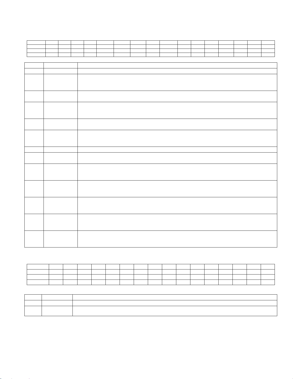
Bit
15
14
13
12
11
10 9 8 7 6 5 4 3 2 1 0
Name - - - -
I2CSPIE
I2CAMI2IE
I2CROIE
I2CGCIE
I2CNACKIE
-
I2CAMIE
I2CTOIE
I2CSTRIE
I2CRXIE
I2CTXIE
I2CSRIE
Reset 0 0 0 0 0 0 0 0 0 0 0 0 0 0 0 0
Access r r r r
rw
rw
rw
rw
rw r rw
rw
rw
rw
rw
rw
BIT
NAME
DESCRIPTION
15:12
Reserved
Reserved. The user should write 0 to these bits.
11
I2CSPIE
I2C Master STOP Interrupt Enable. Setting this bit to ‘1’ will enable an interrupt when a
detection interrupt.
10
I2CAMI2IE
I2C Address Match2 Interrupt Enable. This bit has no function wh en operating in master
mode and is used in slave mode for interrupt enable for I2CSLA2_M slave address.
9
I2CROIE
I2C Master Receiver Overrun Interrupt Enable. Setting this bit to ‘1’ will enable an
disable the receiver overrun detection interrupt.
8
I2CGCIE
I2C General Call Interrupt Enable. This bit has no function when operat i ng in master
mode.
7
I2CNACKIE
I2C Master NACK Interrupt Enable. Setting this bit to ‘1’ will enable an interrupt when a
interrupt.
6
Reserved
Reserved. The user should write 0 to this bit.
5
I2CAMIE
I2C Address Match Interrupt Enable. This bit has no function when operating in master
mode and used in slave mode for interrupt enable for I2CSLA_M slave register.
4
I2CTOIE
I2C Master Timeout Interrupt Enable. Setting this bit to ‘1’ will enable an interrupt when a
interrupt.
3
I2CSTRIE
I2C Master Clock Stretch Interrupt Enable. Setting this bit to ‘1’ will enabl e an interrupt
clock stretch interrupt.
2
I2CRXIE
I2C Master Receive Ready Interrupt Enable. Setting this bit to ‘1’ will enable an interrupt
receive ready interrupt.
1
I2CTXIE
I2C Master Transmit Complete Interrupt Enable. Setting this bit to ‘1’ will enable an
disables transmit complete interrupt.
0
I2CSRIE
I2C Master START Interrupt Enable. Setting this bit to ‘1’ will enable an interrupt when a
detection interrupt.
Bit
15
14
13
12
11
10 9 8 7 6 5 4 3 2 1 0
Name - - - - - - - -
D7
D6
D5
D4
D3
D2
D1
D0
Reset 0 0 0 0 0 0 0 0 0 0 0 0 0 0 0 0
Access r r r r r r r r
rw*
rw*
rw*
rw*
rw*
rw*
rw*
rw*
BIT
NAME
DESCRIPTION
15:8
Reserved
Reserved. The user should write 0 to these bits.
7:0
D[7:0]
Data for I2C transfer is read from or written to this location. The I2C transmit and receive buffers are
separate but both are addressed at this location.
10.2.3 – I
2
C Master Interrupt Enable Register (I2CIE_M)
STOP condition is detected (I2CSPI=1). Clearing this bit to ‘0’ will disable the STOP
interrupt when a receiver overrun condition is detected (I2ROI=1). Clearing this bit to ‘0’ will
NACK is detected (I2CNACKI=1). Clearing this bit to ‘0’ will disable the NACK detection
DS4830A User’s Guide
timeout condition is detected (I2CTOI=1). Clearing this bit to ‘0’ will disable the timeout
when the clock stretch interrupt flag is se t (I2CSTRI=1). Clearing this bit will disable the
when receive ready interrupt flag is set (I2CRXI=1). Clearing this bit to ‘0’ will disable the
interrupt when transmit complete inter rupt flag is set (I2CTXI=1). Clearing this bit to ‘0’
START condition is detected (I2CSRI=1). Cl earing this bit to ‘0’ will disable the START
10.2.4 – I
2
C Master Data Buffer Register (I2CBUF_ M)
* Unrestricted read access. This register can be written to only when I2CBUSY = 0.
92
Page 93

Bit
15
14
13
12
11
10 9 8 7 6 5 4 3 2 1 0
Name
I2CCKH[7:0]
I2CCKL[7:0]
Reset 0 0 0 0 0 0 1 0 0 0 0 0 0 1 0 0
Access
rw
rw
rw
rw
rw
rw
rw
rw
rw
rw
rw
rw
rw
rw
rw
rw
BIT
NAME
DESCRIPTION
15:8
I2CCKH[7:0]
I2C Clock High Period. These bits define the high period of the I
2
C clock. This period is defined
is set to 2.
7:0
I2CCKL[7:0]
I2C Clock Low Period. These bits define the low period of the I
2
C clock. This period is defined by
Bit 7 6 5 4 3 2 1 0
Name
I2CTO7
I2CTO6
I2CTO5
I2CTO4
I2CTO3
I2CTO2
I2CTO1
I2CTO0
Reset 0 0 0 0 0 0 0 0
Access
rw
rw
rw
rw
rw
rw
rw
rw
Bit
15
14
13
12
11
10 9 8 7 6 5 4 3 2 1 0
Name - - - - - - - -
A6
A5
A4
A3
A2
A1
A0
I2CMODE
Reset 0 0 0 0 0 0 0 0 0 0 0 0 0 0 0 0
Access r r r r r r r r
rw
rw
rw
rw
rw
rw
rw
rw
10.2.5 – I
2
C Master Clock Control Register (I2CCK_M)
by the number of system clocks. The high time duration is calculated usin g the following equation:
I2C High Time Period = System Clock Period x (I2CCKH[7:0] + 1)
I2CCKH[7:0] must be set to a minimum va lue of 2 to ensure proper operation. Any value less than 2
the number of system clocks. The low time duration is calculated using the following eq uation:
I2C Low Time Period = System Clock Period x (I2CCKL[7:0] + 1)
I2CCKL[7:0] must be set to a minimum val ue of 4 to ensure proper operation. A ny value less than 4
is set to 4.
10.2.6 – I
2
C Master Timeout Register (I2CTO_M)
DS4830A User’s Guide
The I2CTO_M register determines the length of the timeout interval. The timeout interval is defined by the number of I
periods (SCL high + SCL low). When cleared to 00h, the timeout function is disabled. When set to any other value, the I
controller waits until the timeout expires and sets the I2CTOI flag. The timeout period is:
The timeout timer resets to 0 and starts to count after each of the following events.
10.2.7 – I
2
I
C Timeout = I2C Bit Rate x (I2CTO[7:0] + 1)
• The I2CSTART bit is set.
• The I2CSTOP bit is set.
• Any time that SCL goes low.
2
C Slave Address Register (I2CSLA_M and I2CSLA2_M)
2
C bit
2
C
These register have no function when operating in master mode and are used in slave mode to program the slave
address.
93
Page 94

DS4830A User’s Guide
SECTION 11 – I2C-COMPATIBLE SLAVE INTERFACE
The DS4830A provides an I2C-compatible slave controller that allows communication with a host device and
supports four user-programmable slave addresses. The DS4830A I
operation with a host without clock stretching. The DS4830A I
page for each slave and 8-byte receive FIFO (shared between all four slaves). The DS4830A can also have flash
programming using I
provide system interrupts after each I
2
C bootloading functionality provided by the slave controller. This interface can be set up to
2
C event. Figure 11-1 shows the basic operation flow of the I2C slave controller.
2
C slave interface also has a dedicated 8-byte transmit
The blocks in Figure 11-1 that are shaded are sho wn in more detail in Figure 11-2.
2
C slave controller can support 400kHz I2C
Figure 11-1: Slave I
94
2
C Flow
Page 95

DS4830A User’s Guide
11.1 – Detailed Description
The I2C slave controller has two different modes that can be used to transmit and receive data. The first option
transmits and received data one byte at a time. An advanced mode uses 8-byte buffers for transmiting and receiving
data, which is enabled by setting the TXPG_EN bit in the I2CTXFIE and the FIFO_EN bit in the I2CRXFIE registers.
Using this advanced mode of operation, the DS4830A can support 400kHz I
11.1.1 – Default Operation
2
C slave controller is enabled (I2CCN_S.I2CEN=1) by default. As long as the I2C slave controller is enabled, the
The I
DS4830A I
controller. Prior to the I
configured for necessary I
the slave controller to generate interrupts during I
2
C bootloader can operate. This allows bootloading of blank devices without any setup of the I2C slave
2
C slave controller being used for normal data communication, the I2C SFRs should be
2
C communication. These configurations include setting an I2C slave address and enabling
2
C events. This controller can also operat e as an S M BUS slave.
11.1.2 – Slave Addresses
Prior to communication, an I
responds to two slave addresses. The I
2
C slave address may need to be selected. By default, the I2C slave controller normally
2
C bootloader uses address 34h. This bootloader address c annot be changed
and should not be used as the device slave address for normal communication. The second slave address (default
address 36h) is the address used for communication with the host. This slave address can be programmed by
writing the desired slave address to the I2CSLA_S register. The address contained in the I2CSLA_S register is the
address with the R/W bit. If an address other than 36h is desired, the I2CSLA_S register can be programmed with
this new address.
The DS4830A has three more user-programmable slave addresses that can be programmable using the
I2CSLA2_S, I2CSLA3_S, and I2CSLA4_S registers, respectively. By default, these slave addresses are disabled
and can be individually enabled by writing ‘1’ to the ADDR2EN, ADDR3EN, and ADDR4EN bits, which are defined in
the I2CCN_S register.
2
C slave controller supports the General Call Address, which is 00h with the I2CSLA_S slave register. This
The I
feature can be enabled by setting the I2CCN_S.I2CGCEN bit to a 1.
11.1.3 – I
The I
while SCL is held high. If an I
I2CST_S register, which can cause an interrupt if enabled. The detection of a START brings the I
its idle state. Following a START, the I
to a 1. The I2CBUS bit is also set to a 1 to indicate that the I
11.1.4 – I
The I
while SCL is held high. If an I
I2CST_S register, which can cause an interrupt if enabled. The I2CBUS bit is cleared to 0 following a STOP to
indicate that the I
2
C START Detection
2
C Slave Controller always monitors the I2C bus for an I2C START, which is a high to low transition on SDA
2
C STOP Detection
2
C Slave Controller also always monitors the I2C bus for an I2C STOP, which is a low to high transition on SDA
2
C bus is no longer busy.
2
C START (or restart) condition is detected, the I2C slave sets the I2CSRI bit in the
2
C controller begins to monitor data on the I2C bus and the I2CBUSY bit is set
2
C STOP condition is detected, the I2C slave controller sets the I2CSPI bit in the
2
C bus is currently busy.
11.1.5 – Slave Address Matching
Following an I
host should be the slave address. The I
interaction. The I
2
C START or restart, the I2C slave controller knows that the next byte of data to be transmitted by the
2
C slave controller compares the first 7 bits received to the slave address programmed in the
2
C slave automatically monitors for the slave address without any software
I2CSLA_S register. It also compares the first 7 bits received to the slave addresses programmed in the I2CSLA2_S,
I2CSLA3_S, and I2CSLA4_S registers, if they are enabled. If the received slave address matches with one of
enabled I
2
C Slave addresses, the I2C slave controller does the following steps. This is illustrated in Figure 11-2
(without RX FIFO and TX Pages) and Figure 11-4 (with RX FIFO and TX Pages).
• Transmit an ACK or NACK on the 9th clock based upon the setting of the I2CCN_S.I2CACK bit.
• Set the matched slave address I2CMODE bit with the value of the received R/W bit. This bit can be used by
software to determine if the I
• Sets the I2CST_S.I2CAMI bit to indicate that a slave address match was made. The setting of this bit can
generate an interrupt if enabled. Additionally, the I
2
C slave controller should receive or transmit data.
2
C slave controller sets following values in SLA [3:0] bits in
CUR_SLA register according to the matched slave address.
2
C operation without clock stretching.
2
C controller out of
95
Page 96

DS4830A User’s Guide
Matched Slave Address
CUR_SLA.SLA[3:0]
I2CSLA_S
1
I2CSLA2_S
2
I2CSLA3_S
4
I2CSLA4_S
8
Transmitting
Byte
Receiving
Byte
Y
Receive
Addr[6:0] + R/W
Match
I2CSLA_S[7:1]
?
Transmit
I2CACK
I2CBUSY=0
N
I2CAMI=1
Set
I2CMODE
According to R/W
Detect START
I2CSRI=1
I2CBUS=1
I2CBUSY=1
I2CNACKI =
ACKNOWLEDGE
Transmit Shift
Register Byte,
MSB First
N
Y
I2CBUSY=1
8 Bits
Transmit
?
I2CTXI=1
I2CBUSY=0
Write to
I2CBUF_S
Receive a Bit into
Shift Register
,
MSB first
N
Y
I2CBUSY=1
8 Bits
Received
?
Load Shift
Register into
I2CBUF_S
I2CRXI=1
Send
I2CACK
Y
N
I2CROI=1
Receiver
Full
?
Detect 1
st
SCL
Rising Edge
I2CBUSY=0
Receiving Slave
Address
RECEIVE
ACKNOWLEDGE
• Clears the I2CBUSY flag.
Upon completion of the slave data byte (7 bits of slave address + R/W bit + ACK/NAC K), the I
enters one of the following three states.
• Data Transmit: The slave address matched and the R/W bit is ‘1’. The host is now expecting data from the
DS4830A. The I
2
C slave controller retains control of the SDA line so data can be transmitted to the host. The
host can start clocking data from the slave at any time.
• Data Receive: The slave address is matched and the R/W bit is ‘0’. The host wants to write data to the I
slave. After sending the ACK/NACK bit, the DS4830A releases SDA and is ready to receive a byte of data.
• Wait for START/STOP: The received slave address did not match any enabled slave addresses. The I
controller enters idle state and waits for the next START or STOP condition.
2
C slave controller
2
C
2
C
Figure 11-2: Slave I2C Data Flow
96
Page 97

Shift Register
Address Match
I2CSLA4_S
I2CSLA3_S
I2CSLA2_S
I2CSLA_S
8-Byte
Receive FIFO
MUX
TX0 4 WORDS PAGE
TX2 4 WORDS PAGE
TX3 4 WORDS PAGE
TX4 4 WORDS PAGE
SLA[3:0]
SDA
SCL
SLA[3:0]
Write through
I2CBUF_S
Read through
I2CBUF_S
11.1.6 – Advanced Mode Operation RX FIFO and TX Pages
The DS4830A I
2
C slave controller has a few features that make 400kHz I2C communication without clock stretching
possible.
DS4830A User’s Guide
Figure 11-3: I
The I
address. This is done using the MEM_ADDR[7:0] and PAGE[2:0] bits in the MADDR, MADDR2, MADDR3, and
MADDR4 registers. These register bits 10:0 are used to define start address (SRAM Address) of the memory map
structure and bit 12 is used to define memory rollover boundary between 128 and 256. The I
the memory address of the individual slave address in the read memory address pointer RPNTR register. Each slave
address has dedicated RPNTR, which is selected based on the SLA[3:0] bits. The read address (maintained by
RPNTR) is automatically incremented by 1 word after every write to the I2CBUF_S. The I
256 boundary rollover internally on the read m emory address.
11.1.6.1 – RX FIFO
The DS4830A I
The receive FIFO is controlled using the I2CRXFIE (I
FIFO Status Flags) registers and is read from the I2CBUF_S register. See the individual bit description in I
Controller Register Description section. This FIFO is sho wn in Fi gure 11-3.
11.1.6.2 – Transmit Pages
The I
holds 4 16-bit words. When transmitting data, the controller automatically selects one of the TX pages based upon
the SLA[3:0] bits in the CUR_SLA (Current Slave Address) which is set during a successful slave address match
event. The TX Pages are filled by first setting the SLA[3:0] bits, then writing data to the I2CBUF_S register. I
transmission using the TX Pages is controlled using the I2CTXFIE (I
2
C Transmit Page Status Flags) registers. See the individual bit description in I2C Slave Controller Register
(I
Description section. The TX pages are shown in Figure 11-3.
11.1.6.3 Advanced Mode Memory Address Detection
The I
host. The MADDR_EN bits in the CUR_SLA register enable the memory address to be automatically captured by the
2
C controller. Following an address match with I2CMODE = 0 (Write), the I2C slave controller knows that the next
I
byte of data to be received is the memory address of the memory map and copies the received byte into the
MEM_ADDR[7:0] bits in the MPNTR (Memory address pointer) register with PAGE[2:0] from active slave address.
When the memory address is captured, the MADI bit in the I2CST2_S register will be set, which can generate an
interrupt if enabled. The MPNTR shows the current memory address of the active slave address. To enable memory
address dection, the proper MADDR_EN bit m ust be set and the RX FIFO must be enabled.
2
C Slave Block Diagram with RX FIFO and TX Pages
2
C controller allows the user to define a memory map structure in the user SRAM for each individual slave
2
C controller maintains
2
C controller handles 128 or
2
C controller has an 8-byte receive FIFO. This FIFO is shared among the enabled slave addresses.
2
C controller has four Transmit (TX) pages, each dedicated to a specific slave address. Each of the TX pages
2
C Slave Controller provides an option to automaticcaly detect the memory address being accessed by the
2
C Receive FIFO Interrupt Enable) and I2CRXST (I2C Receive
2
C Transmit Interrupt Enable) and I2XTXFST
2
C Slave
2
C
97
Page 98

Detect I2C Start
I2CSRI = 1
I2CBUS = 1
I2CBUSY = 1
Receive
Addr[6:0] + /R\W
Matched
Enabled Slave
Addresses
Transmit
I2CACK
Set I2CMODE bit
according to /R\W
I2CAMI = 1 and set
CUR_SLA according
to Matched Slave
address
I2CBUSY = 0
No
Yes
Receiving Slave
Address
Transmitting
Data
Update Transmit
Pages at the I
2
C
Start Interrupt
Is Active
Transmit Page
Generated
Threshold
Interrupt
Transmit Shift
Register Byte, MSB
First
8 Bits
Transmit
?
Receive Acknowledge and
set I2CNACKI accordingly
Yes
I2CTXI = 1
I2CBUSY = 0
No
Update Transmit
page with new
transmit data
Receiving Data
Detect 1st SCL Rising
Edge
I2CBUSY = 1
Receive a Bit into
Shift Register MSB
first
8 Bits
Received
?
No
RX FIFO
FULL
?
Set FULL bit
and set
I2CACK = 1
Yes
No
Yes
Load Shift Register
into RX FIFO
Send I2CACK
I2CBUSY = 0
DS4830A User’s Guide
Figure 11-4: Slave I2C Data Flow Using 8-Byte Transmit Page and 8-Byte Receive FIFO
11.1.7 – Transmitting Data
The DS4830A I
the R/W bit set to 1.
2
C Slave Controller enters into data transmission mode after receiving a matching slave address with
11.1.7.1 – Normal Mode Data Transmission
The steps of data transmission are shown in Figure 11-2. Data transmission is started by software loading data into
the I2CBUF_S register. Loading I2CBUF_S causes the I2CBUSY bit in I2CST_S to be set. Once I2CBUSY bit is set,
a write to I2CBUF_S is ignored. The first bit of data (most significant bit) is shifted to SDA when SCL is low. Each of
the next seven bits is then shifted following high to low transitions of SCL.
Following the 8
th
bit data (least significant bit) being shifted to SDA, the SDA line is released by the slave controller.
This allows the host to signal an ACK or NACK during the 9
acknowledge bit following the 9
performs the following tasks:
98
th
SCL rising edge. After the acknowledge bit is sampled, the I2C slave controller
th
clock cycle. The I2C slave controller samples the
Page 99

DS4830A User’s Guide
• Sets the I2CST_S.I2CTXI flag to indicate that the I
generate an interrupt if enabled.
• Sets or clears the I2CST_S.I2CNACKI flag to reflect the received acknowledge bit. The setting of I2CNACKI
can generate an interrupt if enabled.
• Clears the I2CST_S.I2CBUSY flag to indicate that the I
transfer of data.
The detection of an ACK by the I
2
C slave controller maintains control of SDA following the ACK. The next byte to transmit needs to be loaded
The I
2
C slave controller indicates that the host wants to receive another byte of data.
into I2CBUF_S prior to the host starting to clock this next byte.
The detection of a NACK indicates that the host does not want to receive any additional data. The I
controller releases control of SDA following the reception of NACK bit. After the NACK, the slave controller enters
idle state and monitors the I
2
C bus for a START or STOP condition.
11.1.7.2 – Advanced Mode Data Transmission
To achieve 400kHz I
2
C without clock stretch, the DS4830A I2C Controller has 4-word TX Pages for each slave
address. The TXPG_EN bit in the I2CTXFIE register enables the TX PAGEs of the all enabled slave addresses. The
user should pre-fill these 4-word pages to ensure data is available to transmit immedialty following a slave address
match. When data is being transmit, the I
2
C controller automatically selects one of the four TX Pages depending
upon which SLA [3:0] bits are set during the slave a ddress match event.
The individual TX page should be written in the word mode using the I2CBUF_S. See below pseudo code to write
the TX page of I2CSLA2_S address
MOVE DP[0], #01Ch //DP[0] in word mode
MOVE M2[21], #00F2h //Select TX PAGE2 in CUR_SLA
MOVE RPNTR, #0000h //Initialize RPNTR to current read address. When written to 0000h,
//RPNTR will populate with the correct SRAM memory location for
//read data
//Copy word 1
MOVE DP[0], RPNTR //Copy current memory address to the data pointer
MOVE M2[0], @DP[0] //Copy data from @DP[0] to I2CBUF_S register (M2[0])
//I2CBUF_S will load data into TX PAGE
// RPNTR = RPNTR + 1 automatically when data is loaded
//into I2CBUF_S. Rollover handled internal l y.
//Copy word 2
MOVE DP[0], RPNTR //Copy current memory address in the data pointer
MOVE M2[0], @DP[0] //Copy data from @DP[0] to TX PAGE via I2CBUF_S register
//Copy word 3
MOVE DP[0], RPNTR //Copy current memory address in the data pointer
MOVE M2[0], @DP[0] //Copy data from @DP[0] to TX PAGE via I2CBUF_S register
//Copy word 4
MOVE DP[0], RPNTR //Copy current memory address in the data pointer
MOVE M2[0], @DP[0] // Copy data from @DP[0] to TX PAGE via I2CBUF_S register
When TX page is enabled, the SLA[3:0] bits in the CUR_SLA register selects one of the TX pages as shown in
Figure 11-3. The I
2
C controller reads data from the selected TX page and writes to the shift register. When the I2C
controller is transmitting data, the threshold interrupt flag (THSH) in the I2CTXST register will be set when there are
4 bytes are remaining. This can generate an interrupt, if enabled.
2
C slave controller has transmitted a byte. This can
2
C slave controller is not actively participating in the
2
C slave
99
Page 100

DS4830A User’s Guide
11.1.8 – Receiving Data
2
The I
C Slave Controller enters data reception mode after receiving a matching slave address with the R/W bit set to
0. The steps of data reception are shown in Figure 11-2 and Figure 11-4. The reception process begins when the I
slave controller detects the first rising edge of SCL. This rising edge sets I2CBUSY bit to ‘1’ and clocks the first bit
(MSB) of data from SDA into the data shift regist er.
11.1.8.1 – Receiving Data in Normal Mode
When receiving data, the I
register. This allows the I
After a byte (8 bits) of data is received, the I
2
C slave controller uses a double buffer consisting of the I2CBUF_S register and the shift
2
C module to continue receiving data while the previous data byte is being processed.
2
C slave controller attempts to copy the received data from the shift
register to I2CBUF_S and two possible event s c an occur during this attempt.
1. If I2CBUF _S is empty, the I
2
C slave controller copies the data from the shift register into I2CBUF_S. The
I2CRXI flag is set to indicate a received byte is ready for reading. The setting of I2CRXI can generate an
interrupt if enabled. Software can now read data f rom the I2CBUS_S.
2. If I2CBUF _S is full, the data in the shift register cannot be copied into I2CBUF_S. This causes a receive
overrun condition. The receive overrun flag, I2CROI is set which can generate an interrupt if enabled.
I2CBUF_S can be full if it is not read by software following the reception of a previous byte.
When the receive overrun occurs (I2CROI = 1), any new incoming data is not shifted into the I
2
C slave controller.
The controller responds to any bytes received with a NACK regardless of the setting of the I2CACK bit. The receive
overrun condition and the I2CROI flag can only be cleared by software reading received first byte from I2CBU F_S.
When the receive overrun condition is cleared, the I2C slave controller copies the second byte that is received into
I2CBUF, and again sets I2CRXI to indicate a byte of data is received. The I
2
C slave controller resumes its normal
operation in the next SCL clock cycle after I2CROI is cleared. To avoid losing any data, I2CROI must to be cleared
prior to the first SCL clock rising edge of the next byte.
After the 9
participating in a data transaction. The value in I2CACK is transmitted to the host on the 9
assuming the I
th
bit of any byte has been received, the I2CBUSY bit is cleared to indicate that the controller is no longer
2
C slave controller is not operating in receive ove rrun.
th
SCL clock cycle,
11.1.8.2 – Receiving Data in Advanced Mode
As shown in Figure 11-4, when receive FIFO is enabled, the incoming data is copied into the FIFO. The receive
FIFO will set flags in the I2CRXFST register when the FIFO is empty, half full with 4 bytes, or full with 8 bytes of
received data. Interrupts can be generated for these events if the appropriate bits are set in the I2CRXFIE register.
The receive FIFO is read one word at a time by reading the I2CBUF_S register.
11.1.9 – Clock Stretching If slave device cannot receive or transmit another complete byte of data, it may hold SCL low, forcing the master to wait. Data transfer continues when the slave is ready for next byte of data after releasing SCL.
2
C slave controller is capable of holding SCL low at the completion of each byte being transferred. If the I2C
The I
Clock Stretch Enable bit (I2CSTREN) is set to a 1, the I
configured in the I
falling edge of the 9
clock pulse. When the I
slave controller holds SCL low until I2CSTRI is cleared to '0' by software. Figure 11 -5 s hows the I
clock stretching after receiving the 9
2
C Clock Stretch Select bit (I2CSTRS). If I2CSTRS=0, the I2C controller holds SCL low after the
th
clock pulse. If I2CSTRS=1, the I2C controller holds SCL low after the falling edge of the 8th
2
C controller is holding SCL low, the I2C Clock Stretch Interrupt bit (I2CSTRI) is set. The I2C
th
clock of a byte.
2
C controller holds SCL low after the 8th or 9th clock pulse as
2
C slave controller
2
C
100
 Loading...