

Page 1
For LX9 and Nexys-3
Analog Essentials
Getting Started Guide
Overview
Maxim Analog Essentials are a series of plug-in peripheral modules that allow engineers to quickly test, evaluate, and
integrate Maxim components into their hardware/software designs. The modules electrically and physically conform to
the Digilent Pmod™ interface specification and are compatible with any Digilent Pmod-compatible header.
The Analog Essentials collection contains 15 peripheral module boards which are supported by prebuilt hardware and
software projects for various FPGA development boards which are compatible. This version of the Getting Started Guide
is applicable to LX9 and Nexys™-3 boards, both of which are based on Spartan®-6 FPGAs. Users of the other FPGA boards
should refer to different versions of this guide.
Important notes – please read carefully
1. ESD Sensitivity. These modules are intended to be used in an electronic prototyping setting.
They are sensitive to static charge and are subject to damage if proper precautions against
ESD are not taken. When handling these modules, the user should take the same care and
precautions as when working with other ESD sensitive prototypes.
2. Plug – Connector mating. Many plug-in modules contain only one row of six pins, while most Pmod connectors
contain two rows of six contacts each. When plugging in a module with a single row of pins, always plug the
module into the top row of contacts.
3. Plug in with care. Please exercise care when plugging the modules into the Pmod port. The connectors are not
keyed, so it is possible to incorrectly plug in the module and misalign the pins. Although each module includes
series resistors to provide current limiting, in some cases it is still possible to damage the module if it is
incorrectly plugged in.
4. Nexys-3 and LX9 Differences. Most of the instructions in this document refer to both the Nexys-3 board and the
LX9. Instances where a procedure is specific to one board or other will be denoted by the following indicators:
Additional components required
Interested users may wish to obtain additional components to evaluate the following modules:
MAX3231MPMB1 – this module requires a 10mm, 3V lithium primary type coin cell. The generic battery type is CR1025.
Specific examples of this battery are Panasonic #CR1025 and Energizer #CR1025.
MAX31855PMB1 – this module requires a K-Type thermocouple with subminiature connector. Omega series 5SRTC are
suitable (
www.omega.com). Lower cost alternatives may be available via eBay.
1
Page 2

For LX9 and Nexys-3
Part
Functionality
Interface
DS1086LPMB1#
I2C spread-spectrum EconOscillator™
I2C
DS3231MPMB1#
I2C real-time clock
I2C
MAX3232PMB1#
RS-232 transceiver
UART
MAX4824PMB1#
Octal relay driver
GPIO
MAX5216PMB1#
High-performance 16-bit DAC
SPI/GPIO
MAX5487PMB1#
Dual 256-tap digital potentiometer
SPI
MAX5825PMB1#
Octal 12-bit DAC
I2C
MAX7304PMB1#
16-port GPIO and LED driver
I2C
MAX9611PMB1#
Current-sense amplifier with op amp and ADC
I2C
MAX11205PMB1#
16-bit delta-sigma ADC with 2-wire interface
GPIO
MAX14840PMB1#
RS-485 transceiver
UART/GPIO
MAX14850PMB1#
6-channel, 600V galvanic isolator
SPI/UART
MAX31723PMB1#
Digital thermometer
SPI
MAX31855PMB1#
Thermocouple-to-digital converter
SPI
MAX44000PMB1#
Ambient light and proximity sensor
I2C
Analog Essentials
Getting Started Guide
Analog Essentials Collection modules
The table below lists the peripheral modules included in the collection, along with a description and interface type.
Included Files
The top level of the hardware design is a Xilinx ISE® Project Navigator Project (.xise) for Xilinx ISE version 13.4. The
Verilog-based HDL design instantiates the Microblaze™ core, the support hardware required to run the Microblaze, and
the peripherals (I
development kit (SDK) project which includes a demonstration software application to evaluate each module’s
functionality. The lower level c-code driver routines are portable to the user’s own software projects.
2
C, SPI, GPIO, and UART) which interface to the Pmod ports. This is supplied as a Xilinx software
Prerequisites
• Xilinx ISE13.4 or a later version must be installed on the development PC, along with a license for Xilinx EDK/SDK.
• To modify the FPGA code or the software, the user should have a basic understanding of Xilinx Project Navigator
(ISE) development tools, I
• Maxim Analog Essential Project Source (downloadable from
• One or more of the peripheral modules boards in the Analog Essentials collection.
2
C, SPI, GPIO buses, ANSI C, and (ideally) the Xilinx Embedded Development Kit toolset.
www.maxim-ic.com/FPGA-modules)
2
Page 3
For LX9 and Nexys-3
Analog Essentials
Getting Started Guide
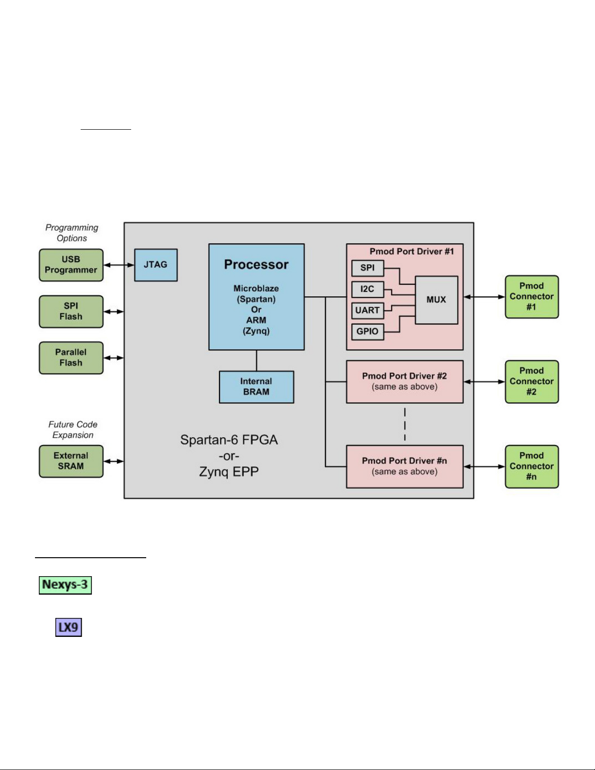
Typical System Architecture
Below is a generalized block diagram for the architecture implemented in the FPGA project. One of the key elements is
the logic block that drives each Pmod port. Each Pmod port driver contains a dedicated I
octal GPIO port. Any of these can be quickly connected to the Pmod port via software control. (The multiplexer setting is
controlled by another internal GPIO port.) This eliminates the need to reprogram the FPGA during testing and evaluation
of various peripheral modules.
2
C port, SPI port, UART, and
Board specific notes
Digilent Nexys-3: This FPGA board contains 4 Pmod connectors, all of which are driven by the
logic/hardware resources as shown in the above diagram.
Avnet LX9: Although the LX9 board contains 2 Pmod connectors, the FPGA does not contain a
sufficient number of gates to implement two complete copies of the drivers as shown above.
Therefore, only one of the Pmod ports on the LX9 (“J5”) is driven as shown. Pmod connector “J4” is
driven by an octal GPIO interface block and not utilized by the supplied software.
3
Page 4

For LX9 and Nexys-3
Analog Essentials
Getting Started Guide
Getting Started
Introduction
With small Microblaze FPGA designs, it is typical for the binary executable program to fit entirely within the internal
block RAM of the FPGA. In these cases, the FPGA can be programmed by simply downloading a single bit-stream file,
which contains both the FPGA logic and the binary executable for the running software on the processor. However, the
size of the sample programs for the Analog Essentials collection exceeds the capacity of the internal block RAM memory.
Therefore, external memory (outside the FPGA) must be utilized for both program and data storage. Because of this,
loading the program is a multistep process. The first step loads, then executes a boot loader. The boot loader then loads
the .elf (executable software file for the Microblaze). While this is not as simple as downloading a single file, it
represents the situation encountered with many real-world applications.
The first section of this guide leads the user through the process of loading the project into the FPGA board for
execution. The section following that outlines the basic steps in modifying the project.
Overview: Downloading the Example/Demonstration Application
Below is a high-level overview of the steps required to download and run the FPGA project. Detailed instructions for
each step are provided in the following pages.
1. From Maxim’s website, download the latest version of the Maxim Analog Essentials project that corresponds to
your FPGA board. The code will be delivered as a .zip file. Visit
the link to MAXPMBAE which takes you to the Quick-View page for Analog Essentials. From there, click on the
“Technical Documents” to access the software downloads.
2. Extract the .zip file to a directory on your machine (direction location is arbitrary, but for the purposes of this
document, it will be c:\designs\maxim\v1_4). See Appendix B in this document for a complete description of
the included files.
3. Open the Xilinx SDK (Windows Start Menu > Xilinx ISE 13.4 > EDK > Xilinx Software Development Kit).
4. Download the bitstream (.bit) file to the board. This bitstream contains the FPGA hardware design and software
bootloader.
5. Open Hyperterminal or a similar communications program to communicate with FPGA board.
6. Use Xilinx SDK/XMD debugger console to download and run executable file (.elf) on the Microblaze.
www.maxim-ic.com/fpga-modules, then click on
4
Page 5
For LX9 and Nexys-3
Analog Essentials
Getting Started Guide
Detailed Steps: Downloading the Example/Demonstration Application
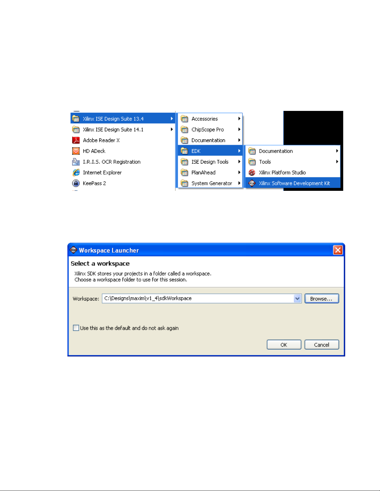
1. Opening the SDK
a. From the Windows Start Menu, Open the Xilinx SDK as shown below
.
b. SDK will prompt for a workspace directory, the location where the software project is located. This
directory is generally a subfolder within a Xilinx ISE/EDK project and will include board support files, as
well as (.c) and (.h) files. Be certain to choose the correct Workspace directory. For this project, it will be
C:\Designs\maxim\v1_4\sdkWorkspace (as shown below).
c. Click OK to the prompt shown above and SDK will open. The Xilinx SDK is based on an Eclipse-based IDE,
so it will be a familiar flow for many software developers.
5
Page 6
For LX9 and Nexys-3
Analog Essentials
Getting Started Guide
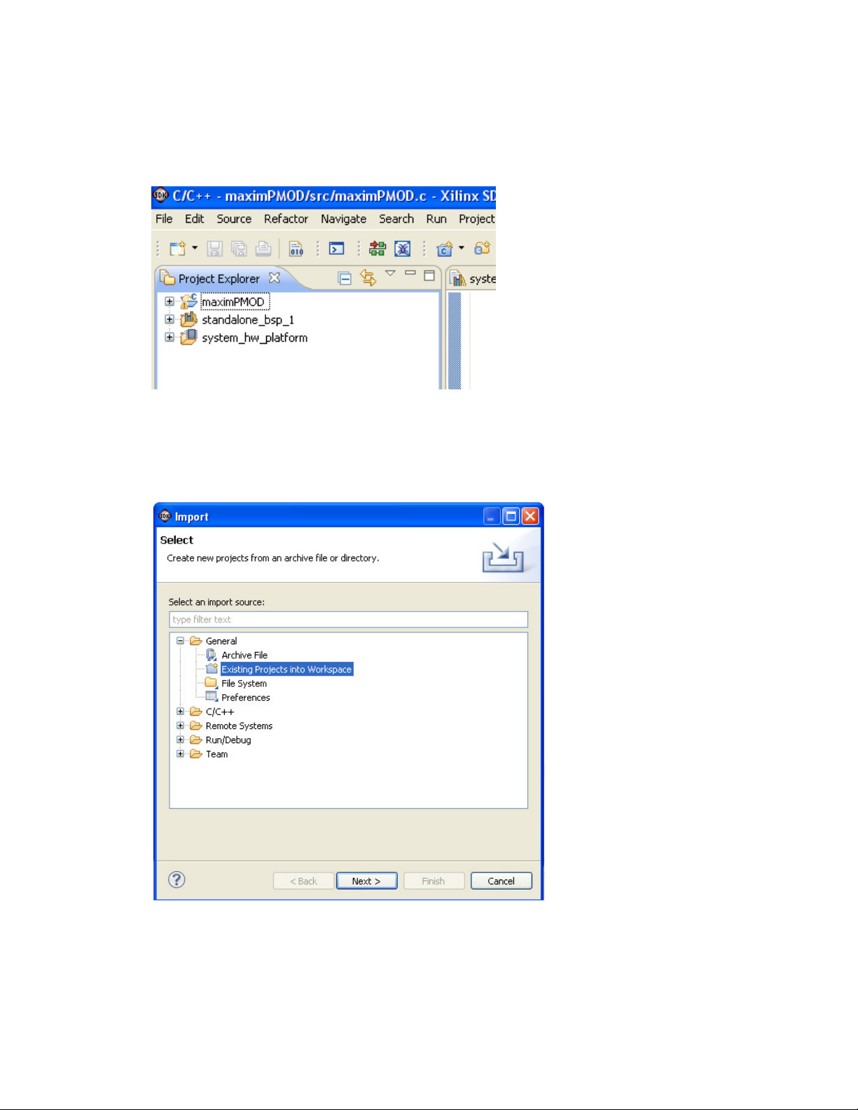
d. Review the SDK IDE. The Project Explorer in the upper left tab should have three components as shown
in the image below. If all three subfolders are present, you can skip the next step.
If the Project Explorer does not contain these three subfolders, launch the File > Import menu, expand
e.
the General tab and select Existing Projects into Workspace. Click Next. Set the root directory to
C:\designs\maxim\v1_4\sdkWorkspace, and the missing
with their checkboxes checked. Click Finish to import the projects.
projects should appear in SDK Project explorer
6
Page 7
For LX9 and Nexys-3
Analog Essentials
Getting Started Guide
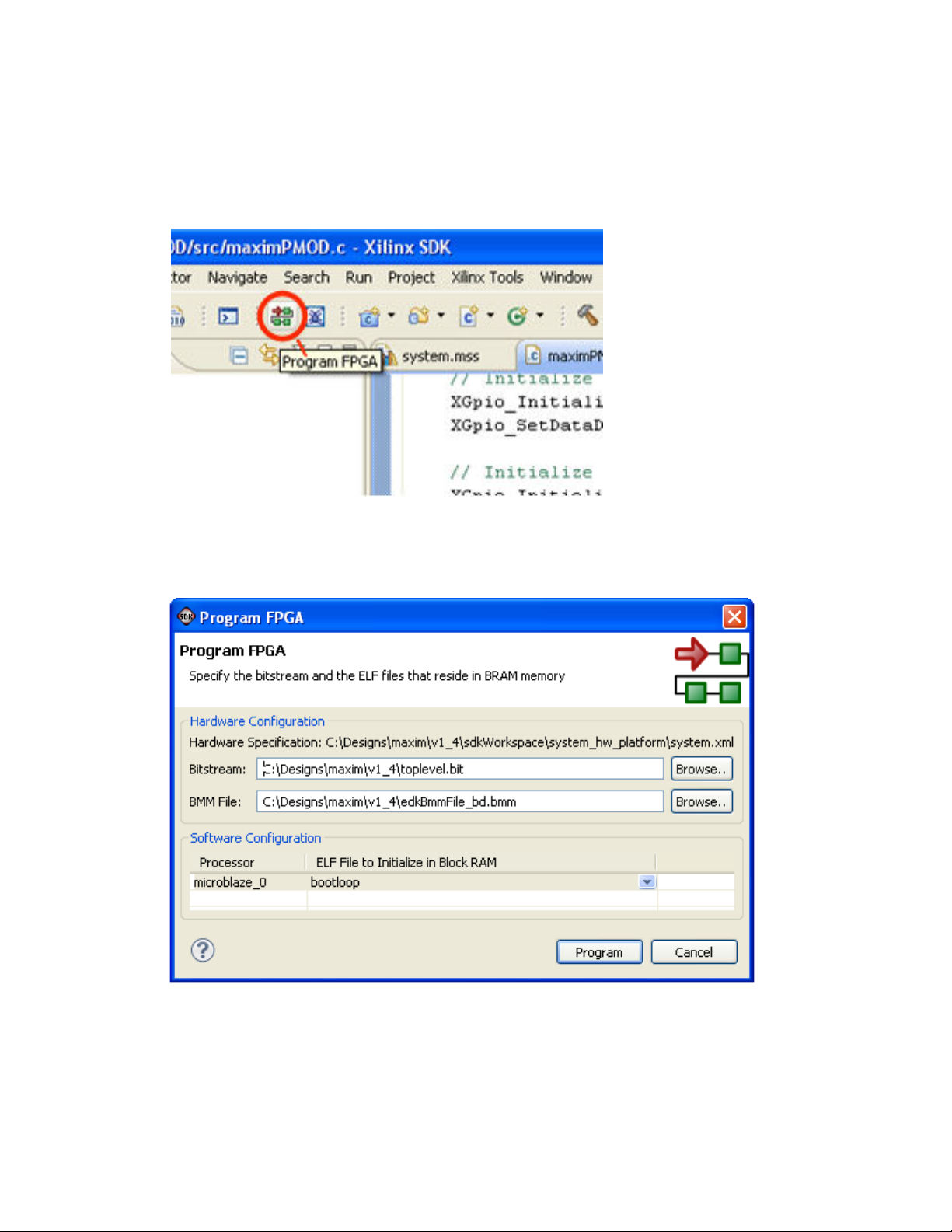
2. Downloading the bitstream (.bit) file to the board.
a. Click on the Program FPGA icon (which looks like a green chain of devices):
b. The Program FPGA dialog box will appear. From here, an FPGA bitstream is selected as well as an FPGA
bmm file and a (.elf) file to load into the Microblaze memory as shown below. Be sure to select the
toplevel.bit file, the edkBmmFile_bd.bmm, and the bootloop file as shown, then select Program.
7
Page 8

For LX9 and Nexys-3
Analog Essentials
Getting Started Guide
It takes approximately 10 seconds to download the FPGA and a message box indicating “FPGA
configuration complete” will appear.
A brief note summarizing the previous steps:
As discussed earlier in this document, the code size of this program exceeds that available in block
memory internal to the FPGA, necessitating the use of the external RAM. This requires a multi-stage
loading process implemented with a boot-loader. This operates a bit differently from smaller programs
where the entire FPGA configuration data and executable code is contained in one .bit file and is loaded
in one step
The bitstream (.bit) file is used to configure the FPGA and initiate the bootloading process. This
bitstream contains all the configuration information necessary to initialize the FPGA with the gate level
hardware design, including block memories, which are used for the base Microblaze memory.
The (.bmm) file provides the location of block RAM memories (internal to the FPGA) that are used as
codespace for the Microblaze. The (.elf) file contains the instructions that represent the Microblaze
executable program. That file will be loaded into external pseudostatic RAM (PSRAM) using the Xilinx
debugger in a subsequent step, right after we set up PC communications in the next step.
8
Page 9

For LX9 and Nexys-3
Analog Essentials
Getting Started Guide
3. Setting Up the PC for Communication
Before loading the executable software file, the serial communications program should be opened so that the
PC is ready to communicate with the FPGA board once the software begins executing. The example/demo
software running on the host board communicates with the PC via a USB port set up to emulate a serial port
(UART). To establish this communication link, the PC must be configured with the appropriate Windows drivers.
While the drivers for both the LX9 and Nexys-3 are functionally equivalent, the boards use different USB-UART
bridge ICs. Therefore, the boards use different drivers. Also, a suitable communications program such as
HyperTerminal should be invoked.
a. The Nexys-3 utilizes the FTDI USB UART, so you need to install FTDI’s virtual COM port drivers. These
may be obtained from the FTDI
operating system generally performs this step automatically the first time the USB on the host is
connected to the PC’s USB port, so the driver might already be installed.
The LX9 also utilizes a USB UART in a similar fashion. However, the USB UART IC used on the LX9 is the
CP2102 from Silicon Labs. Follow the same instructions as above but install the driver from the Silicon
Labs
website. (http://www.silabs.com/products/mcu/pages/usbtouartbridgevcpdrivers.aspx)
Once installed, Windows will assign a previously unused COM port. Use Control Panel | System | Device
Manager to determine the COM port number. (It will be named USB Serial Port). Make a note of which
COM port this is. That information is needed in the next step.
website. (www.ftdichip.com/Drivers/VCP.h) Note: the Windows®
b. Next, a terminal emulation program needs to be installed and launched. For Windows XP® and earlier
systems, the Hyperterminal program is the usual choice. However, since Hyperterminal was eliminated
from Windows 7, it may be necessary to locate an alternative. Several are available, one of which is
called “PuTTY” (
follows: bits per second: 115,200
www.putty.org). Whatever program you choose, the communication should be set up as
; data bits: 8; parity: none; stop bits: 1; and flow control: none.
9
Page 10

For LX9 and Nexys-3
Analog Essentials
Getting Started Guide
4. Using Xilinx SDK/XMD to download and run executable file (.elf) on the Microblaze.
a. Click the XMD Console tab if it isn’t already showing, as shown below.
b. At the XMD% prompt at the bottom of the XMD console, issue the following commands.
1. Use “pwd” and “cd” to navigate to the following directory:
C:\designs\maxim\v1_4\sdkWorkspace\maximPMOD\Debug
2. connect mb mdm
3. dow maximPMOD.elf
4. run
c. At this point, the application will be running on the Microblaze and the USB UART/Hyperterminal should
show a menu like the one below. This is the top level menu for the module example programs.
10
Page 11

For LX9 and Nexys-3
Analog Essentials
Getting Started Guide
5. Running the demonstration programs
Peripheral modules can now be placed into the appropriate PMOD port (Ports A..D) and a menu selection made
to exercise the module’s functionality. For example, place the MAX31723 module into the PMOD B port*. When
prompted for a Pmod port, select “B”.
The submenu for the MAX31723 peripheral module will appear and the module may be exercised using the
appropriate keyboard-selected commands. The submenu for the MAX31723 is shown below.
Important note when running the demo programs:
Many of the programs allow incrementing and decrementing the primary registers or program values using the
arrow keys. In these cases, the Up and Down arrows will increment and decrement the value in small steps
(generally, but not always by an increment of one). The left and right arrow keys will increment and decrement
the value in larger steps. This option is not indicated on the submenus.
*Note: The Nexys-3 board uses all 4 available Pmod ports which are considered PortA - PortD running left to
right across the top of the board. The LX9 board only uses the Pmod port labeled “J5” so the port selection step
does not apply when using this board.
11
Page 12

For LX9 and Nexys-3
Analog Essentials
Getting Started Guide
The remaining sections of this document are intended to serve only as brief outlines of and
introductions to the steps necessary to modify the hardware and software for this project. Detailed
instructions on these procedures and the design tools are beyond the scope of this document.
Modifying the Project C Code
This section provides detailed information on changing the project source code, recompiling, and redownloading.
1. Modifying the C code and recompiling
a. To modify the C code, navigate in the Project Explorer to the maximPMOD.c file.
b. Double-click on maximPMOD.c. This will open the file in the source code editor. The file maximPMOD.c
contains the main() function for the demonstration application. The main() function initializes several
board peripherals, then prints a menu to the USB UART on the host board. Each menu choice calls an
underlying menu function which allows functions of each peripheral module to be tested.
12
Page 13

For LX9 and Nexys-3
Analog Essentials
Getting Started Guide
c. Make an edit to the maximPMOD.c file. We will uncomment a line of code to add a printf statement to
the boot-up screen. This printf statement is located about half-way through the file maximPMOD.c.
d. After un-commenting the “Hello World” line, select File > Save from the menu. This will force the IDE to
recompile with the code change. The contents of the console should be as shown below.
e. The last two lines are critical. If elfcheck passes, then the (.elf) executable for the Microblaze has been
built successfully and is ready for download via the XMD window and “dow” command. Note: if the
Microblaze is already running, the XMD command “stop” can be issued to stop the Microblaze. “Run”
will then redownload the Microblaze and run the program.
13
Page 14

For LX9 and Nexys-3
Analog Essentials
Getting Started Guide
2. Optional: Setting the memory locations and generating a linker script
In small software designs, the source code can be merged directly into the FPGA bitstream and downloaded with
normal FPGA bitstream tools. However, larger software designs (like this one) that exceed the internal code
space must be downloaded to and run from external memory. Using the linker script allows the user to select
the target memory location.
a. Highlight the maximPMOD project under Project Explorer, and choose Menu > Xilinx Tools > Generate
Linker Script as follows.
14
Page 15

For LX9 and Nexys-3
Analog Essentials
Getting Started Guide
b. [ LX9 version. Skip to step “c” for Nexys-3.] This will bring up the linker script menu as shown below.
From this window the code, data, heap/stack section placement can be chosen. For the application
demonstration, this should be set to MCB3_LPDDR_S0_AXI_BASEADDR.
Skip to step “d”.
15
Page 16

For LX9 and Nexys-3
Analog Essentials
Getting Started Guide
c. [ Nexys-3. See above for LX9] This will bring up the linker script menu as shown below.
From this window the code, data, heap/stack section placement can be chosen. For the application
demonstration, this should be set to Digilent_Shared_Mem_Bus_Max_PSRAM_BASEADDR.
d. Clicking Generate will rebuild the (.elf) file with the memory locations set to the external PSRAM
memory.
16
Page 17

For LX9 and Nexys-3
Analog Essentials
Getting Started Guide
Detailed Steps: Opening the ISE Project to View the HDL and Launch EDK
1. Open Xilinx Project Navigator 13.4
a. Verify that the tools are using the correct directory by looking at the directory displayed at the top of
the ISE screen. Xilinx Tools default to opening the last used directory. Be careful to make sure that you
are not working on an older revision of the design. If ISE is not using the latest directory, then close the
project and re-open the latest project (in this case, C:\designs\maxim\v1_4\top.xise).
b. The top level source code for this project is contained within top.v. Double-click on top.v to open the ISE
Verilog editor.
17
Page 18

For LX9 and Nexys-3
Analog Essentials
Getting Started Guide
c. Once any changes are made, the project can be rebuilt by selecting Generate Programming File from
the Design tab (see below). This will generate a new toplevel.bit file.
18
Page 19

For LX9 and Nexys-3
Analog Essentials
Getting Started Guide
2. Open the EDK/XMP project (Microblaze Core/Peripherals)
a. Highlight and double-click on “cpu1 – system(system.xmp)” as shown below. Changes to the Microblaze
core and the internal peripherals can be configured here. Examples of this are adding additional I
ports or changing the baud rate on the UARTs.
2
C
b. After making any changes to the Microblaze within EDK, run DRC and Generate netlist, then rebuild the
ISE project to incorporate those changes into the base bitstream (toplevel.bit).
c. Re-export the design to SDK by clicking on the Export to SDK icon in the upper left menu area.
19
Page 20

For LX9 and Nexys-3
Analog Essentials
Getting Started Guide
d. This will launch a dialog box asking to export the design or export and launch SDK. At the dialog box,
click the Export & Launch SDK button, or if the SDK is already running, choose Export Only. This process
will bring the SDK project .mss/.xml files in sync with the EDK project.
20
Page 21

For LX9 and Nexys-3
Analog Essentials
Getting Started Guide
Appendix A: Project Notes
1. Each active Pmod port has a dedicated I2C port, SPI port UART and octal GPIO. These communications
peripherals are multiplexed to the physical ports via an HDL designed multiplexer. (Refer to the diagram in the
Typical System Architecture section.) An example of this can be seen in the maximPMOD.c file at about the
midpoint, as shown in the clip below.
Also, note that all 4 Pmod ports on the Nexys-3 board are driven in this manner. However, due to gate count
limitation in the LX9, only one of its Pmod ports is actively driven by this configuration.
2. The functions in maximDeviceSpecificUtilities.c are used to access the major functionality provided by the
Maxim ICs. In general, these functions return an integer value (TRUE/FALSE) that describes whether or not the
function successfully completed. Although it is not required to check this return value, it is good programming
practice to do so.
3. Functions will typically require a peripheral port address. These ports are assigned sequentially from the sets of
2
C, SPI, UART and GPIO peripherals in the design, and are named from ports 0..3. (Again, the Nexys-3 design
I
includes 4 ports and the LX9 design includes one port.) Examples include:
a. XPAR_IIC_0_BASEADDR, XPAR_IIC_1_BASEADDR, XPAR_IIC_2_BASEADDR, etc.
b. XPAR_SPI_0_BASEADDR, XPAR_SPI_1_BASEADDR, etc
c. XPAR_AXI_UARTLITE_0_BASEADDR, XPAR_AXI_UARTLITE_0_BASEADDR, etc
4. GPIO calls receive a pointer to a Xilinx XGpio instance
a. XGpio portA;
b. XGpio_Initialize(&portA, XPAR_AXI_GPIO_0_DEVICE_ID);
Since the functions return TRUE/FALSE as a pass/fail indication, when the functions return a value, it is passed back to
the calling function via a pointer.
21
Page 22

For LX9 and Nexys-3
Analog Essentials
Getting Started Guide
Appendix B: Project Structure and Key Filenames
22
Page 23

For LX9 and Nexys-3
Analog Essentials
Getting Started Guide
All trademarks are property of their respective owners.
23
 Loading...