

Page 1

AVAILABLE
USER GUIDE
78M6631
Firmware Description Document
October 10, 2011
Rev 2
UG_6631_078
Page 2

78M6631 Firmware Description Document UG_6631_078
Maxim Integrated 160 Rio Robles, San Jose, CA 95134 USA 1-408-601-1000
Maxim cannot assume responsibility for use of any circuitry other than circuitry entirely embodied in a Maxim product. No circuit patent licenses are implied.
Maxim reserves the right to change the circuitry and specifications without notice at any time. The parametric values (min and max limits) shown in the Electrical
Characteristics table are guaranteed. Other parametric values quoted in this data sheet are provided for guidance.
©
XXXX Maxim Integrated
The Maxim logo and Maxim Integrated are trademarks of Maxim Integrated Products, Inc.
Page 3

UG_6631_078 78M6631 Firmware Description Document
Table of Contents
1 Introduction ................................................................................................................................... 5
2 Functional Description .................................................................................................................. 7
2.1 Initialization and Startup ........................................................................................................... 7
2.2 Measurements and Signal Processing Flow ............................................................................. 7
2.2.1 Description of Measurement Equations........................................................................ 7
2.2.2 Front-End and Input Stage .......................................................................................... 8
2.2.3 Voltage and Current RMS Calculation ......................................................................... 9
2.2.4 Active, Reactive and Apparent Power Calculation ...................................................... 10
2.2.5 Voltage and Current Harmonics and Fundamental Measurement............................... 11
2.2.6 Power Harmonics and Fundamental Measurement .................................................... 11
2.2.7 Power Factor Calculation ........................................................................................... 12
2.2.8 Line Frequency ......................................................................................................... 12
2.2.9 Accumulation Interval ................................................................................................ 12
2.2.10 Zero Crossing Detector ............................................................................................. 12
2.2.11 Sine and Cosine Reference ....................................................................................... 13
2.2.12 High-Pass Filters ....................................................................................................... 13
2.3 Configuration and Control ...................................................................................................... 14
2.3.1 Input Registers .......................................................................................................... 14
2.3.2 Sensors Configuration ............................................................................................... 14
2.3.3 Updating Flash .......................................................................................................... 14
2.3.4 Scaling ...................................................................................................................... 14
2.3.5 Calibration ................................................................................................................. 15
2.3.6 Phase Error Compensation........................................................................................ 16
2.3.7 Limit (Alarms) Settings .............................................................................................. 16
2.3.8 Creep Threshold........................................................................................................ 16
2.3.9 Digital I/O Configuration............................................................................................. 16
3 Serial Peripheral Interface (SPI) .................................................................................................. 17
4 Serial Communication and CLI ................................................................................................... 18
4.1 CLI Interface .......................................................................................................................... 18
5 Register Descriptions .................................................................................................................. 19
5.1 Command Register ................................................................................................................ 19
5.2 Status Register ...................................................................................................................... 20
5.3 Measurement Results Register .............................................................................................. 21
5.3.1 High-Rate Results Registers...................................................................................... 23
5.4 Parameters Configuration ...................................................................................................... 24
5.4.1 Scaling ...................................................................................................................... 24
5.4.2 Alarms Limit Setting................................................................................................... 24
5.4.3 Phase Error Compensation........................................................................................ 24
5.4.4 Digital I/O Configuration............................................................................................. 25
5.4.5 Calibration and Configuration Variables ..................................................................... 25
6 System Connection Diagram Examples ..................................................................................... 26
7 Command Line Interface (CLI) Description ................................................................................ 29
7.1 Identification and Information Commands............................................................................... 29
7.2 Reset Commands .................................................................................................................. 29
7.3 Data Access Commands ........................................................................................................ 29
7.3.1 Individual Address Read ............................................................................................ 30
7.3.2 Consecutive Read ..................................................................................................... 30
7.3.3 Block Reads .............................................................................................................. 30
7.3.4 Concatenated Reads ................................................................................................. 30
7.3.5 Repeat Command ..................................................................................................... 31
8 Contact Information ..................................................................................................................... 32
Revision History .................................................................................................................................. 32
Rev 2 3
Page 4

78M6631 Firmware Description Document UG_6631_078
Tables
Table 1: Measurement Equations Definitions ........................................................................................... 7
Table 2: SPI Command Description ....................................................................................................... 17
Figures
Figure 1. Simplified Connection Diagram of a 3-Phase Wye System ........................................................ 5
Figure 2. Simplified Connection Diagram of a 3-Phase Delta System ....................................................... 6
Figure 3. Input Stage Signal Processing Path .......................................................................................... 8
Figure 4. Voltage and Current RMS Calculations ..................................................................................... 9
Figure 5. Power and Power Factor Signal Processing Chain .................................................................. 10
Figure 6. Voltage and Current Harmonics and Fundamental Measurements .......................................... 11
Figure 7. Power Harmonic and Fundamental Measurements ................................................................. 11
Figure 8. 3-Phase System Calibration Test Setup Example .................................................................... 15
4 Rev 2
Page 5
UG_6631_078 78M6631 Firmware Description Document
A
Neutral
B
C
VC
VB
VA
LOAD A
LOAD B
LOAD C
IAP
IAN
IBP
IBN
ICP
ICN
V3P3A
A
Neutral
B
C
78M6631
D/Y
Teridian is a trademark of Maxim Integrated Products, Inc.
1 Introduction
This document describes the 78M6631 firmware (6631_3PH_6S_URT_B21), which can be used with the
Teridian™ 78M6631 energy measurement IC. This firmware provides measurements for a 3-phase
system along with simple methods for calibration, configuration, and access to metrology data. This
document contains the following sections:
• Functional Description: Signal Processing Flow, Functions, Calibration, and Operations
• Configuration and Control: Configurability and Settings
• Communications: Communication Interfaces and Protocols Description
The calculations are done on each of the phases individually and the aggregate measurements are also
available as follows:
• Voltage rms (Phase A, B, C)
• Current rms (Phase A, B, C)
• Active Power (Phase A, B, C)
• Apparent Power (Phase A, B, C)
• Reactive Power (Phase A, B, C)
• Power Factor (Phase A, B, C)
• Line Frequency
The firmware also provides measurement results on fundamentals and harmonics. Section 2.2.5
describes how to access and configure harmonics measurements.
The firmware supports Delta and Wye Configurations, the configuration is selectable through a dedicated
pin (D/Y) of the 78M6631 or by modifying the configuration register.
Figure 1. Simplified Connection Diagram of a 3-Phase Wye System
Rev 2 5
Page 6
78M6631 Firmware Description Document UG_6631_078
A
B
C
VC
VB
VA
LOAD A-C
IAP
IAN
IBP
IBN
ICP
ICN
V3P3A
A
B
C
78M6631
LOAD A-B
LOAD B-C
D/Y
Figure 2. Simplified Connection Diagram of a 3-Phase Delta System
All measurement calculations are computed by the 78M6631 and accessible through serial interfaces:
UART0 on the TX and RX pins and the Serial Peripheral Interface (SPI).
On the UART, the CLI (Command Line Interface) handles the serial communications .The CLI provides
access to internal data and allows issuing commands through the serial port. Section 3 provides details
on serial port default configuration and Section 4 describes the CLI commands.
Note that the firmware does not support I
2
C, RTC (real-time clock), and battery modes.
6 Rev 2
Page 7

UG_6631_078 78M6631 Firmware Description Document
Symbol
Parameter
Equation
PF
Power Factor
P/S
2 Functional Description
This section summarizes the functional operation of the 78M6631 firmware. Refer to the IC data sheet
and application notes for more information on terminologies and detailed IC operation.
2.1 Initialization and Startup
Upon power-up, both MPU and Compute Engine (CE) cores start executing the application code from
designated blocks of flash memory. The parameters and defaults are copied from Flash memory into
RAM and accessible (R/W) through the communication interfaces and utilized by the firmware.
After the initialization phase, the firmware starts regular operations and signal processing.
The user can modify any parameters specified as input register, however the modified values are volatile
and will be lost during a power-down or reset. To permanently save the value of the input registers it is
necessary to store them to flash. A section in this document describes which registers can be saved into
flash memory and the relevant command.
2.2 Measurements and Signal Processing Flow
2.2.1 Description of Measurement Equations
The firmware provides the user with continuously updated measurement data. Table 1 lists the basic
measurement equations.
Table 1: Measurement Equations Definitions
V RMS Voltage
I RMS Current
P Active Power
Q Reactive Power
S Apparent Power S = V * I
PA N/A Phase Angle ACOS (P/S)
V = √∑
I = √∑
P = ∑
Q = ∑
(i(t) * vq(t))
2
v(t)
2
i(t)
(i(t) * v(t))
The integrated AFE and CE function as a data acquisition system, controlled by the MPU. The lowvoltage analog input signals are sampled and stored in CE DRAM where they are processed by the CE.
This firmware utilizes an effective sampling rate of 2521 samples per second. The sampling rate is
referred to each individual channel.
The CE, a dedicated 32-bit signal processor, performs the computations necessary to perform all the
measurements. The CE calculations and processes include:
• Multiplication of each current sample with its associated voltage sample to obtain the energy per
sample (when multiplied with the constant sample time).
• Frequency-insensitive delay cancellation on all channels (to compensate for the delay between
samples caused by the multiplexing scheme).
• 90° phase shifter (for VAR calculations).
• Monitoring of the input signal frequency.
• Monitoring of the input signal amplitude.
• Scaling of the processed samples based on calibration coefficients.
Rev 2 7
Page 8
78M6631 Firmware Description Document UG_6631_078
SINC
3
DECIMATOR
IA
CROSS-
POINT
∆Σ
MODULATOR
PRECISION
REFERENCE
IA_RAW
VA_RAW
IB_RAW
VA1
F
ADC
+
250mv
ADC
X
X
X
X
VB_RAW
IA1
VA
IB
VB
IC
VC
IC_RAW
VC_RAW
IoffsA
VoffsA
Φ COMP
PCOMPA
TEMPERATURE
SENSOR
Temperature
Compensation
IgainA
+
VgainA
+
VB1
X
X
X
X
IB1
IoffsB
VoffsB
Φ COMP
PCOMPB
IgainB
+
VgainB
+
VC1
X
X
X
X
IC1
IoffsC
VoffsC
Φ COMP
IgainC
+
VgainC
+
PCOMPC
Φ COMP
Φ COMP
Φ COMP
At the end of each accumulation interval, these measurements are provided to the MPU for postprocessing. Alternate multiplexer cycles also gather measurements of the IC’s junction temperature for
additional compensation in the MPU. Post-processing functions handled by the MPU at the end of every
accumulation interval include:
• Compensation for environmental variables
• Calculation of apparent power, power factor, phase angle, and line frequency
• Comparing of measurement outputs to configurable alarm thresholds
• Scaling and formatting of output measurement data
• Updating of all output registers (data and alarm status)
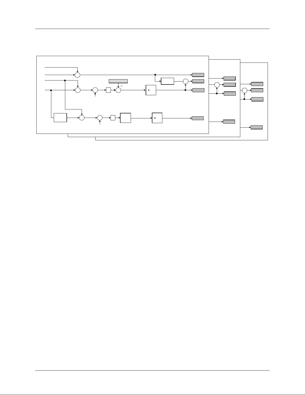
2.2.2 Front-End and Input Stage
Figure 3 shows the ADC signal path and signal processing for the voltage and current input channels.
Figure 3. Input Stage Signal Processing Path
The gray boxes are the gain calibration input registers. These registers can be modified by the user or by
the gain calibration routine for both voltage and current channels.
The voltage and current inputs channels are also temperature compensated. A compensation algorithm
based on the reading of an on-chip temperature sensor, corrects the gain in order to maintain the
accuracy across the temperature range.
The phase compensation block allows to digitally correct phase errors. These errors are usually
introduced by the voltage/current transformers or external filters. The phase error is calibrated by
introducing a time delay or a time advance, specified in the phase adjust registers.
The registers PCompA, PCompB, and PCompC can be modified by the user.
A configurable high-pass filter (HPF) in both voltage and current signal path removes any DC content
(offset) in the inputs.
8 Rev 2
Page 9
UG_6631_078 78M6631 Firmware Description Document
=
Vn
N
=
In
N
IC_SQ
VC_SQ
IC_SQSUM
VC_SQSUM
IC_RAW
IrmsC
VrmsC
IB_SUM IB_OFFS
VC1
N
∑
N-
1
X
n=
0
∑
N-1
n=0
∑
N-1
n=0
PHASE C
IC1
VC_RAW
VB_SUM
VB_OFFS
∑
N-
1
n=
0
N
N
X
N
+
Iroff
IB_SQ
VB_SQ
IB_SQSUM
VB_SQSUM
IB_RAW
IrmsB
VrmsB
IB_SUM IB_OFFS
VB1
N
∑
N-
1
X
n=
0
∑
N-1
n=0
∑
N-1
n=0
PHASE B
IB1
VA_RAW
VB_SUM
VB_OFFS
∑
N-
1
n=
0
N
N
X
N
+
Iroff
IA_SQ
VA_SQ
IA_SQSUM
VA_SQSUM
IA_RAW
Irms A
Vrms A
IA_SUM
IA_OFFS
VA1
N
X
PHASE A
IA1
VA_RAW
VA_SUM
VA_OFFS
N
N
X
N
+
Iroff
∑
N-1
n=0
∑
N-1
n=0
∑
N-1
n=0
∑
N-1
n=0
2.2.3 Voltage and Current RMS Calculation
As shown in Figure 4, the voltage and current channels ADC output samples are used to continually
compute the RMS (root mean square). The RMS is obtained by performing the square sum of the
instantaneous samples of voltage and current over a time interval (commonly referred as accumulation
time) and then performing a square root of the result:
In Figure 4, the output registers are represented in gray.
Figure 4. Voltage and Current RMS Calculations
Rev 2 9
Page 10
78M6631 Firmware Description Document UG_6631_078
IC1
VC1
WATTSUM_C
Quadrature
Delay
X
LPF
Σ
(TMP)
LPF
Σ
+
X
WATT C
VAR C
Poff
X
VA C
INVERSE
X
PF C
VqC
N
N
∑
N-1
n=0
VrmsC
IrmsC
(TMP)
PHASE C
IB1
VB1
WATTSUM_B
Quadrature
Delay
X
LPF
Σ
(TMP)
LPF
Σ
+
X
WATT B
VAR B
Poff
X
VA B
INVERSE
X
PF B
VqB
N
N
∑
N-1
n=0
VrmsB
IrmsB
(TMP)
PHASE B
IA1
VA1
WATTSUM_A
Quadrature
Delay
X
LPF
Σ
(TMP)
LPF
Σ
+
X
WATT A
VAR A
Poff
X
VA A
INVERSE
X
PF A
VqA
N
N
∑
N-1
n=0
VrmsA
IrmsA
(TMP)
PHASE A
2.2.4 Active, Reactive and Apparent Power Calculation
Figure 5 shows the signal processing chain for active and reactive power calculations.
Figure 5. Power and Power Factor Signal Processing Chain
Active Power
The instantaneous power is obtained multiplying instantaneous voltage and current samples. The product
is then averaged over N conversions (accumulation time) to compute active power (WATTA, WATTB and
WATTC), the aggregate value (WATTS) is the sum of the 3 phases active power average.
Apparent Power
The apparent power (VA-A, VA-B, VA-C) is the product of rms voltage (VrmsA, VrmsB, and VrmsC) and
rms current (IrmsA, IrmsB, IrmsC):
VA = I
RMS
x V
RMS
Reactive Power
The reactive power is calculated as multiplication of instantaneous samples of current (IA1, IB1, IC1) and
the instantaneous quadrature voltage (VqA, VqB, VqC). The quadrature voltage is obtained through a 90°
phase shift (quadrature delay) of the voltage samples. The samples are then averaged over the
accumulation time interval and updated in the VARA, VARB, and VARC registers.
10 Rev 2
Page 11

UG_6631_078 78M6631 Firmware Description Document
SINE(t)
VA1
X
X
COSINE(t)
SINE(t)
IA1
X
X
COSINE(t)
VSINE_A
VCOS_A
ISINE_A
ICOS_A
Vfund C
Ifund C
Vrms A
Vharm C
Irms A
Iharm C
N
N
N
N
∑
N-1
n=0
∑
N-1
n=0
∑
N-1
n=0
∑
N-1
n=0
PHASE C
X
2
+ Y
2
X
Y
X
2
+ Y
2
X
Y
V harm B
X2 - YI
2
X
YI
X2 - YI
2
X
YI
SINE(t)
VA1
X
X
COSINE(t)
SINE(t)
IA1
X
X
COSINE(t)
VSINE_A
VCOS_A
ISINE_A
ICOS_A
Vfund B
Ifund B
Vrms A
Vharm B
Irms A
Iharm B
N
N
N
N
∑
N-1
n=0
∑
N-1
n=0
∑
N-1
n=0
∑
N-1
n=0
PHASE B
X
2
+ Y
2
X
Y
X
2
+ Y
2
X
Y
X2 - YI
2
X
YI
X
2
- YI
2
X
YI
SINE(t)
VA1
X
X
COSINE(t)
SINE(t)
IA1
X
X
COSINE(t)
VSINE_A
VCOS_A
ISINE_A
ICOS_A
Vfund A
Ifund A
Vrms A
VharmA
Irms A
Iharm A
N
N
N
N
∑
N-1
n=0
∑
N-1
n=0
∑
N-1
n=0
∑
N-1
n=0
PHASE A
X
2
+ Y
2
X
Y
X
2
+ Y
2
X
Y
X2 - YI
2
X
YI
X2 - YI
2
X
YI
SINE(t)
VC1
X
X
COSINE(t)
SINE(t)
IC1
X
X
COSINE(t)
VSINE_C
VCOS_C
ISINE_C
ICOS_C
Complex
Multiply
Complex
Conjugate
QfunC
PfunC
PharmC
∑
N-1
n=0
∑
N-1
n=0
∑
N-1
n=0
∑
N-1
n=0
WATT C
PHASE C
SINE(t)
VB1
X
X
COSINE(t)
SINE(t)
IB1
X
X
COSINE(t)
VSINE_B
VCOS_B
ISINE_B
ICOS_B
Complex
Multiply
Complex
Conjugate
QfunB
PfunB
PharmB
∑
N-1
n=0
∑
N-1
n=0
∑
N-1
n=0
PHASE B
WATT B
SINE(t)
VA1
X
X
COSINE(t)
SINE(t)
IA1
X
X
COSINE(t)
VSINE_A
VCOS_A
ISINE_A
ICOS_A
Complex
Multiply
Complex
Conjugate
QfunA
PfunA
PharmA
∑
N-1
n=0
∑
N-1
n=0
∑
N-1
n=0
∑
N-1
n=0
PHASE A
WATT A
2.2.5 Voltage and Current Harmonics and Fundamental Measurement
The 78M6631 firmware allows measurement of the harmonic and fundamental components. To enable
the harmonics and fundamental measurements bit 5 of the command register must be set to 1.
Harmonic voltage (Vharm) and current (Iharm) are calculated with the quadratic subtraction of the
Fundamental results from the RMS results (the square root of RMS squared minus Fundamental
squared).
Figure 6 shows the harmonic and fundamental components.
Figure 6. Voltage and Current Harmonics and Fundamental Measurements
2.2.6 Power Harmonics and Fundamental Measurement
Harmonic Power (Pharm) is calculated by subtracting Fundamental Power (Pfund) from total active
power (Watts).
Quadrature Harmonic Power (Qhram) is calculated by subtracting Fundamental Quadrature Power
(Qfund) from Total Reactive Power (VARs).
Rev 2 11
Figure 7. Power Harmonic and Fundamental Measurements
Page 12

78M6631 Firmware Description Document UG_6631_078
2.2.7 Power Factor Calculation
The 78M6631 provides a direct power factor measurement simultaneously for phase A, phase B, and
phase C. Power factor in an AC circuit is defined as the ratio of the active power flowing to the load to the
apparent power. The power factor measurement is defined in terms of “import” or “export” referring to the
direction of the power in the system.
Power factor is reported for all phases, and a weighted average is also provided. All values will be
between -1.0 and +1.0 and can be scaled by the user to the desired resolution.
2.2.8 Line Frequency
Frequency (FREQ) is both an input register and an output (result) register (low-rate). If the bit
”FREQ” (Command Register bit 4) is set to 0, the line frequency (measured from a phase reference)
is stored in this variable. If bit ”FREQ” is instead set to 1, the value contained in this register will be
utilized by the firmware. The default value is in this case 60Hz, and can be modified by the user.
This variable is used to set the frequency of the sine/cosine generator for fundamental and harmonic
calculations. It can also be set to a harmonic or an arbitrary unrelated frequency to measure the
amplitude of that frequency.
Phase Reference: The phase reference is calculated on the difference VA-VB-VC.
2.2.9 Accumulation Interval
The low-rate calculation/results are performed over a time interval referred as accumulation interval. The
accumulation interval can be modified by the user through Accum Register. The Accum register is an
unsigned integer containing the minimum number of high-rate samples that define the low-rate interval.
For example, with a value of 0x7D0 the accumulation interval results in:
Accumulation Inteval =
Resulting in an accumulation interval of 793 ms.
Effective Accumulation Interval
The register Divisor reports the value of the effective accumulation interval as number of high-rate
samples. Referring to the processing flow diagrams, it represents the divisor (N) for low-rate accumulated
results.
Line-Lock
The Command Register bit “LINELOCK” can be used to lock the low-rate interval to incoming Line
Voltage Cycles. When set, the low-rate sample period will end after the first low-to-high zero crossing of
the Phase A Voltage input occurs after the Minimum Accumulation time has elapsed. The Actual
Accumulation Interval will span an integer number of line cycles.
When LINELOCK is not set, the Accumulation Interval will equal the number of high rate samples
specified in the Accum register.
1
Accum
2.2.10 Zero Crossing Detector
The polarity of the Phase Reference is used by the zero-crossing detection logic to determine the
start and end of consecutive line cycles. It is used for frequency measurement, to determine the
backstep for quadrature voltage delay lines, and to lock the low-rate computation cycle to the line
frequency. A 3/4-cycle holdoff timer is used to prevent noise and harmonics from registering as
additional zero crossings.
12 Rev 2
Page 13

UG_6631_078 78M6631 Firmware Description Document
2.2.11 Sine and Cosine Reference
An internal Sine/Cosine oscillator generates waveforms used by the fundamental and harmonic
result calculations. The frequency of this oscillator is set by the FREQ variable. It is generally set to
the line frequency. The phase is unrelated and unimportant.
2.2.12 High-Pass Filters
An alternative to offset calibration is dynamic offset removal. This can be accomplished with either
lump-sum removal or a more gradual averaged reduction. The latter is similar to high-pass filtering,
but without phase distortion. All three methods are controlled by the HPF coefficient register. This is
a 9 bit value indicating how much of the measured offset (median) to remove each low-rate sample
period.
When HPFcoeff = 0, the last value in the offset registers is subtracted from the respective inputs.
This is the state that offset calibration uses. When HPFcoeff = 1.0 (0x100) the offset registers are
loaded with the measured offset (median) every low-rate sample. This is lump-sum offset removal.
When HPFcoeff is a fraction – say .75 (0xc0), 75% of the measured offset and 25% of the old
register value is used. Low values of HPFcoeff give very low HPF corner frequencies.
Rev 2 13
Page 14

78M6631 Firmware Description Document UG_6631_078
2.3 Configuration and Control
2.3.1 Input Registers
The following parameters are configurable by the user via input registers:
• Sensor range and configuration
• Calibration targets and coefficients
• Alarm Thresholds and Mask Settings
2.3.2 Sensors Configuration
A few parameters specific to the voltage and current sensors and their connections require one time
configuration.
Sensor Output Range
The sensor’s output needs to be adapted to the ADC input range (+/- 250mVpk). In case of a Current
Transformer (CT), the burden resistor value should be selected in order to match the maximum ADC input
voltage at the maximum load current that need to be measured. Similarly consideration applies for the
voltage sensor (Voltage Dividers or Voltage Transformers).
Delta/Wye Configuration Selection
The different connections can be selected through the external dedicated D/Y pin or through commands
over the UART or SPI interfaces. At power-on or reset the D/Y pin is sampled and its status determines
the set of equations enabling the proper configuration. After the initialization, the configuration can then
be changed by the user through the command register. Bit 2 (Delta) set to 0 selects the Wye
configuration while Bit 2 set to 1 selects the Delta configuration.
The status of the Delta bit in the command register is always overwritten at power-on with the status of
the D/Y pin.
2.3.3 Updating Flash
The values of sev eral input registers can be updated by the user at run-time. A flash update routine is
provided to sav e the values of various registers as default. To save the registers values to flash memory,
see the section describing the command register.
2.3.4 Scaling
Scaling registers provide a means for the user to adapt the meaning of the results to the end
application. There are separate scaling registers for RMS voltage, RMS current, power, and power
factor, but each register covers all three phases.
By default, scaling registers are set so that result LSBs represent one millivolt, milliamp, or milliwatt,
millihertz, Power factor is scaled to 1 LSB = .001.
Example
The scaling registers contain full-scale values in units selected by the user. For example, 50 amps full
scale with a resolution of 1 milliamp will be a scaling register value of 50000.
14 Rev 2
Page 15

UG_6631_078 78M6631 Firmware Description Document
A
Neutral
B
C
VC
VB
VA
IAP
IAN
IBP
IBN
ICP
ICN
V3P3A
A
Neutral
B
C
78M6631
AC SOURCE
AC
LOAD
AC
LOAD
AC
LOAD
NOTE: ONE OR MORE
PHASES CAN BE
CALIBRATED
SIMULTANEOUSLY
D/Y
2.3.5 Calibration
As with any measurement system, there are also multiple sets of coefficients that are used to
compensate for system inaccuracies. Input registers for all coefficients can be manually modified and
saved to flash. Alternatively, high level calibration routines can be invoked. These routines automatically
determine the coefficients for common parameters and save them to flash memory. The different types of
compensation parameters include:
• Voltage: gain and offset for voltage sense circuit
• Current: gain and offset for current sense circuit
• Phase: voltage-to-current phase offset introduced by transformer or filters in sense circuits
• Temperature: offset for junction temperature at room temp
• Temperature: coefficients for temperature curve
• RMS and Power offset: fixed offsets for voltage and current and power at light loads
The calibration routines compensate for sensors and system inaccuracy. The new coefficients computed
during calibration can be stored in the on-chip flash.
In order to perform a calibration, an external stable AC source (Voltage/Current) and AC load are
required. The calibration routines have a target voltage and current (Register Itarget) used for all phases
to match. The target calibration voltage and current values are specified in the registers Vtarget and
Itarget.
Figure 8. 3-Phase System Calibration Test Setup Example
Rev 2 15
Page 16

78M6631 Firmware Description Document UG_6631_078
To calibrate the voltage and current the following steps are required:
• AC Source and Load: The calibration routine needs a stable source and load. The source and load
can be applied to a single phase, two phases or all three phases.
• Selection of Target Values: Before launching the calibration the target value (voltage/current) must
be set. During calibration the gains will be adjusted to match the target voltage and/or current.
• Selection of the Gain to Calibrate and Launch: the gain calibration can be performed on one
phase or multiple phases and can be voltage, current or both simultaneously. The control register
allows the selection of the channel to calibrate and the launch of the calibration routine.
Upon a successful calibration the command register will have the bits set for calibration reset to 0.
Upon unsuccessful calibration the command register will have the bits set for all failing channels.
2.3.6 Phase Error Compensation
The 78M6631 is designed to function with a variety of current transducers, including those that induce
inherent phase errors. A phase error of 0.1° to 0.3° is not uncommon for a current transformer (CT).
These phase errors can vary from part to part, and they must be corrected to achieve accurate power
readings. The errors associated with phase mismatch are particularly noticeable at low power factors. The
78M6631 provides a means of digitally calibrating these small phase errors by introducing a time delay or
a time advance.
A Phase Compensation register is provided for each of the 3 phases. The range for phase
compensation is ±20° at 50 Hz. Phase compensation registers are set to 0.0 by default. Positive
values increase delay on voltages relative to currents. The default is ideal when using resistive
shunts for current measurement. But a compensation value will be required to compensate for the
induced delay of a current transformer or external filter.
Phase compensation registers use a signed (two’s complement) fixed-point notation. Bits 15:0 are
the fractional part and bits 31:16 are the integer part. The range is -3.0 to +3.999 high-rate samples.
The phase compensation registers are PhComp A, PhComp B, and PhComp C.
2.3.7 Limit (Alarms) Settings
The Limit registers set limits on result values causing Status Register bits to be set when a limit
threshold is exceeded. Limit registers use the same scaling applied to results and, as such, are userdefinable.
Sticky Bits
The user has the option to choose which Status Register bits will clear automatically once an alarm
condition no longer exists. Each bit in the Sticky Register corresponds to the same bit in the Status
Register. When a Sticky bit is set, the same bit in the Status register will not clear automatically.
They can only be cleared by writing the Status Register.
2.3.8 Creep Threshold
The 78M6631 includes a “no-load” detection feature that eliminates what is commonly referred as “meter
creep.” Meter creep is defined as power (or energy) that is read by the system when there is no load
attached. The FW sets the current to zero reading when its value falls below the programmable threshold.
2.3.9 Digital I/O Configuration
Five digital I/Os (DIOs) can be controlled by the user through the serial communication interfaces. These
digital I/Os are set as output and their logic levels are controlled through MASK registers. See Section
5.4.4.
16 Rev 2
Page 17

UG_6631_078 78M6631 Firmware Description Document
(From 78M6631)
(From 78M6631)
Comm and
Description
MPU SPI interrupt is generated if xx xxxx is not equal to 0.
3 Serial Peripheral Interface (SPI)
The 78M6631 has an on-chip SPI interface. The interface is slave (only) and can communicate directly on
the MPU data bus without FW overhead.
A typical SPI transaction is as follows: While PCSZ is high, the port is held in an initialized/reset state.
During this state, PSDO is held in high-Z state and all transitions on PCLK and PSDI are ignored. When
PCSZ falls, the port will begin the transaction on the first rising edge of PCLK. A transaction consists of
an 8-bit command, a 16-bit address, and then one or more bytes of data. The transaction ends when
PCSZ is raised. Some transactions may consist of a command only.
Table 2: SPI Command Description
11xx xxxx ADDR D0 ... DN Output data on PSDO is read from RAM starting with byte at ADDR.
ADDR will auto-increment until PCSZ is raised.
1100 0000 ADDR D0 ... DN Output data on PSDO is read from RAM starting with byte at ADDR.
ADDR will auto-increment until PCSZ is raised.
No MPU SPI interrupt is generated because xx xxxx equals 0.
10xx xxxx ADDR D0 ... DN Input data on PSDI is written to RAM starting with byte at ADDR.
ADDR will auto-increment until PCSZ is raised.
MPU SPI interrupt is generated if xx xxxx is not equal to 0.
1000 0000 ADDR D0 ... DN Input data on PSDI is written to RAM starting with byte at ADDR.
ADDR will auto-increment until PCSZ is raised.
No MPU SPI interrupt is generated because xx xxxx equals 0.
CMD ADDR D0 ... DN CMD and ADDR are available to the CPU in IORAM
D0 … DN are ignored.
MPU SPI interrupt is generated
Rev 2 17
Page 18

78M6631 Firmware Description Document UG_6631_078
4 Serial Communication and CLI
The serial communication with the 78M6631 takes place over a UART (UART0) interface. The default
settings for the UART of the 78M6631, as implemented in this firmware, are given below:
Baud Rate: 38400bps
Data Bits: 8
Parity: None
Stop Bits: 1
Flow Control: None
The host’s serial interface port is required to implement these settings on its UART. To verify
communication between the host and the 78M6631, the host must send a <CR> (carriage return) to the
78M6631. Communication is verified when the 78M6631 returns a > (greater than sign) known as the
command prompt. An example is given below:
The host sends the following to the 78M6631:
<CR>
The 78M6631 sends the following back to the host:
>
4.1 CLI Interface
The Command Line Interface (CLI) provides a simple ASCII interface to access input and output registers
and to invoke commands. The CLI interface connects to a HyperTerminal or any other terminal emulation
SW. The CLI interface can also be used to interface to a host processor.
18 Rev 2
Page 19

UG_6631_078 78M6631 Firmware Description Document
Flash
Stored
23
-
N
Not Used
19
CG
N
Calibrate Gain Command (1=calibrate)
18
CT N Calibrate Temperature
Enable Fundamental/Harmonic
Calculations
Allow Frequency to set Sine/Cosine
period
Y Selects DELTA / WYE Configuration
1:0
–
N/A
CE reserved
5 Register Descriptions
All register are 32 bits (4 bytes) and are on ”longword” (4 byte) boundaries. All register addresses are the
same internally for both SPI and CLI (UART) user interfaces. However, the SPI interface has the ability to
address individual bytes while the CLI interface can only address entire longwords. So SPI addresses
contain two extra low order bits.
5.1 Command Register
Command register can be accessed through UART/CLI (address 0x42) or SPI (address 0x108). The
Command Register allows the user to select voltage or current channels to be calibrated. Also allows
enabling or disabling of harmonic/fundamental measurements. The following table shows the Command
Register bit assignment. The default value of the Command Register is 0x00000000.
Bit Name
31 – N CE reserved
30:28 – N MPU reserved
27 CO N Calibrate Offset
26 VA N Select VA Channel For Calibration
25 VB N Select VB Channel For Calibration
24 VC N Select VC Channel For Calibration
22 IA N Select IA Channel For Calibration
21 IB N Select IB Channel For Calibration
20 IC N Select IC Channel For Calibration
17:6 – N/A MPU reserved
Description
5 FUND Y
4 FREQ Y
3 LINELOCK Y Locks low rate period to line cycles
2 YD
Rev 2 19
0=Wye ; 1=Delta
Page 20

78M6631 Firmware Description Document UG_6631_078
CLI Address
0xF5
SPI Address
0x3D4
Bit
Description / Comment
1, 0
Not Used
2
Minimum Temperature Alarm (Under Temperature)
9
OverCurrent phase A
10
Voltage Imbalance phase C
11
Voltage Imbalance phase B
12
15
Under-Voltage phase A
16
Over-Voltage phase C
17
Over-Voltage phase B
18
Over-Voltage phase A
23 -30
Not Used
31
Command Done
5.2 Status Register
The status register contains alarms and system status flags that can be monitored by the host processor.
Alarms thresholds can be set through the corresponding registers.
Status Register
3 Maximum Temperature Alarm. (Over Temperature)
4 UnderCurrent phase C
5 UnderCurrent phase B
6 UnderCurrent phase A
7 OverCurrent phase C
8 OverCurrent phase B
Voltage Imbalance phase A
13 Under-Voltage phase C
14 Under-Voltage phase B
20 Power Factor phase C
21 Power Factor phase B
22 Power Factor phase A
Sticky Bits Register
The sticky bit register at address 0xF3 (CLI) and 0x3CC (SPI) allows the user to set the mode of the
status register bit. Each bit can individually be programmed to clear automatically once an alarm
condition no longer exists or to holds its status until cleared by writing to the status register.
20 Rev 2
Page 21

UG_6631_078 78M6631 Firmware Description Document
Temperature
18A 628 Die Temperature
Line frequency
(unsigned)
Effective Accumulation Interval
(number of high-rate cycles)
rms voltage Phase A
(unsigned)
rms voltage Phase B
(unsigned)
rms voltage Phase C
(unsigned)
rms Current Phase A
(unsigned)
rms Current Phase B
(unsigned)
rms Current Phase C
(unsigned)
rms Current Total
(unsigned)
Active Power Phase A
Active Power Phase B
Active Power Phase C
Total active power
Apparent power - phase A
(unsigned)
Apparent power - phase B
Apparent power - phase C
(unsigned)
Reactive power - phase B
Reactive power - phase C
Total reactive power
5.3 Measurement Results Register
CLI
Output
Frequency 151 544 Hz
Address
(hex)
LSB
SPI
Address
(hex)
LSB Comment
Divisor
Vrms A 154 550 mVrms
Vrms B 156 558 mVrms
Vrms C 158 560 mVrms
Irms A 155 554 mArms
Irms B
Irms C 159 564 mArms
Irms 153 548 mArms
Watt A 164 590 mW
Watt B 165 594 mW
Watt C 166 598 mW
Watts
44 110
157
167
59C mW
55C mArms
VA-A 16C 5B0 mW
VA-B 16D 5B4 mW
VA-C 16E 5B8 mW
VAs 16F 5BC mW Total apparent power
VarA 168 5A0 mW
VarB 169 5A4 mW
VarC
Vars 16B 5AC mW
16A 5A8
mW
Reactive power - phase A
(unsigned)
Rev 2 21
Page 22

78M6631 Firmware Description Document UG_6631_078
PFA
15A 568 Power Factor Phase A
PFB
15B 58C Power Factor Phase B
PFC
15C 570 Power Factor Phase C
Fundamental rms voltage Phase A
Fundamental rms voltage Phase B
(unsigned)
Fundamental rms voltage Phase C
(unsigned)
Fundamental rms voltage Phase A
(unsigned)
Fundamental rms voltage Phase B
Fundamental rms voltage Phase C
Fundamental rms voltage (Aggregate)
(unsigned)
PfundA
170 5C0
mVrms
Active Fundamental power A
PfundB
171 5C4
mVrms
Active Fundamental power B
PfundC
172 5C8
mVrms
Active Fundamental power C
Pfund
189 624
mVrms
Active Fundamental power (Aggregate)
Reactive Fundamental power
Harmonic voltage – phase A
(unsigned)
Harmonic voltage – phase B
(unsigned)
Harmonic voltage – phase C
(unsigned)
IharmA
17C 5F0
mVrms
Harmonic current phase A
IharmB
17D 5F4
mVrms
Harmonic current phase B
IharmC
17E 5F8
mVrms
Harmonic current phase C
Iharm
17F
5FC
mVrms
Harmonic current (Aggregate)
PharmA
174 5D0
mVrms
Active Harmonic power A
PharmB
175
5D4
mVrms
Active Harmonic power B
PharmC
176 5D8
mVrms
Active Harmonic power C
Pharm
177 5DC
mVrms
Active Harmonic power (Aggregate)
Output
Register
CLI
Address
(hex)
LSB
SPI
Address
(hex)
LSB Comment
VfundA 180 600 mVrms
VfundB
VfundC 182 608 mVrms
IfundA 178 5E0 mVrms
IfundB 179 5E4 mVrms
IfundC 17A 608 mVrms
Ifund
QfundA
QfundB
QfundC
Qfund 189 624 mVrms
181 604
17B
186
187
188
5EC mVrms
618 mVrms Reactive Fundamental power A
61C mVrms Reactive Fundamental power B
620 mVrms Reactive Fundamental power C
mVrms
(unsigned)
(unsigned)
(unsigned)
(Aggregate)
VharmA 183 60C mVrms
VharmB 184 610 mVrms
VharmC 185 614 mVrms
22 Rev 2
Page 23

UG_6631_078 78M6631 Firmware Description Document
(Hex)
(Hex)
VB
20
80
Voltage – Phase B
IB
22
88
Current – Phase B
5.3.1 High-Rate Results Registers
There is a set of registers that are updated at a high rate. Although accessible by both UART and SPI, it
is recommended to use SPI. The SPI interface if faster than the UART and does not require any FW
overhead and latency, having direct access to the memory.
Register
Name
VA 10 40 Voltage – Phase A
VC 30 C0 Voltage – Phase C
VqA 11 44 Quadrature Voltage A
VqB 21 84 Quadrature Voltage B
VqC 31 C4 Quadrature Voltage C
IA 12 48 Current – Phase A
IC 32 C8 Current – Phase C
Vsine 40 100 Sine reference
Vcosine 41 104 Cosine reference
CLI
Addr
SPI
Addr
Description
Rev 2 23
Page 24

78M6631 Firmware Description Document UG_6631_078
(Hex)
(Hex)
VrmsMax
10C
430
Maximum RMS voltage/phase
unsigned
Y
0
CLI
SPI
5.4 Parameters Configuration
These registers are defined as input registers. The values of the input registers can be updated by the
user at run-time. A flash update routine is provided to save the values of various registers as default
(check the Flash Stored column in the following tables).
Save Input Register Values to Flash Memory
To save the register values to flash memory, it is necessary to write the following value to the Command
Register: 0x5920008. Once saved, the latest saved values will become the new defaults.
5.4.1 Scaling
Input
Register
Iscale 101 404 Scaling for RMS currents unsigned Y 50000
Vscale 100 400 Scaling for RMS voltages unsigned Y 667000
Pscale 102 408 Scaling for Power results unsigned Y 33350000
PFscale 117 45C Scaling for Power Factor unsigned Y 1000
Fscale 107 41C Scaling for Frequency unsigned Y 1000
Tscale 108 420 Scaling for Temperature unsigned Y 1000
CLI
Address
(Hex)
SPI
Address
(Hex)
Scaling Notes
Flash
Stored
Default
5.4.2 Alarms Limit Setting
Input
Register
IrmsMax 10A 428 Maximum RMS current/phase unsigned Y 0
IrmsMin 109 424 Minimum RMS current/phase unsigned Y 0
VrmsMin 10B 42C Minimum RMS voltage/phase unsigned Y 0
PFmin 10E 438 Minimum Power Factor/phase unsigned Y 0
Tmin 10F 43C Minimum Temperature Y 0
Tmax 110 440 Maxim um Temperature Y 0
VmaxDelta 10D 434
CLI
Address
SPI
Address
Alarm Limits
(Note: 0* disables item)
Maximum line-to-line Voltage
Imbalance
Notes
unsigned
Flash
Stored
Y 0
Default
5.4.3 Phase Error Compensation
Input
Register
PcompA 104 410 Phase compensation A signed Y 0
PcompB 105 414 Phase compensation B signed Y 0
PcompC 106 418 Phase compensation C signed Y 0
24 Rev 2
Address
(Hex)
Address
(Hex)
Phase Compensation Notes
Flash
Stored
Default
Page 25

UG_6631_078 78M6631 Firmware Description Document
Mask1
111
444
DIO3 Control
Boolean Y 0
CLI
SPI
Ttarget
11A
468
Calibration target for Temperature
unsigned
Y
22000
Tcurr
FC
3F0
Current Temperature
signed
IoffsA
16
58
Offset calibration for A current
signed Y 0
5.4.4 Digital I/O Configuration
Input
Register
Mask2 112 448 DIO14 Control Boolean Y 0
Mask3 113 44C DIO15 Control Boolean Y 0
Mask4 114 450 DIO17 Control Boolean Y 0
Mask5 115 569 DIO43 Control Boolean Y 0
CLI
Address
(Hex)
SPI
Address
(Hex)
Phase Compensation Notes
Flash
Stored
Default
5.4.5 Calibration and Configuration Variables
Input
Register
HPFcoeffI 103 40C High-pass filter coefficient (Current) unsigned Y 0x100
HPFcoeffV 11F 47C High-pass filter coefficient (Voltage) unsigned Y 0x100
Itarget 118 460 Calibration target for RMS currents unsigned Y 50000
Vtarget 119 464 Calibration target for RMS voltages unsigned Y 667000
Toffs 11C 470 Offset for Temperature signed 0
Accum 43 10C Accumulation Interval unsigned Y 2000
CalCyc 11B 46C Calibration Cycles to Average unsigned Y 5
Tgain F8 3E0 Temperature gain (DegScale) signed 2768
Tnom FB 3EC Nominal Temperature signed Y 0xD000000
Address
(Hex)
Address
(Hex)
Calibration Variables Notes
Flash
Stored
Default
IgainA 14 50 Gain calibration for A current unsigned Y 0x4000
IgainB 24 90 Gain calibration for B current unsigned Y 0x4000
IgainC 34 D0 Gain calibration for C current unsigned Y 0x4000
VgainA 13 4C Gain calibration for A voltage unsigned Y 0x4000
VgainB 23 8C Gain calibration for B voltage unsigned Y 0x4000
VgainC 33 CC Gain calibration for C voltage unsigned Y 0x4000
IoffsB 26 98 Offset calibration for B current signed Y 0
IoffsC 36 D8 Offset calibration for C current signed Y 0
VoffsA 15 54 Offset calibration for A voltage signed Y 0
VoffsB 25 94 Offset calibration for B voltage signed Y 0
VoffsC 35 D4 Offset calibration for C voltage signed Y 0
Iroff 11D 474 Current RMS Offset Adjust unsigned Y 0
Poff 11E 478 Power Offset Adjust unsigned Y 0
Rev 2 25
Page 26

78M6631 Firmware Description Document UG_6631_078
A
Neutral
B
C
VC
VB
VA
LOAD A
LOAD B
LOAD C
IAP
IAN
IBP
IBN
ICP
ICN
V3P3A
A
Neutral
B
C
78M6631
D/Y
6 System Connection Diagram Examples
This section shows supported 3-phase connections and configurations
3-Phase 4-Wire
The 3-phase 4-wire configuration has a connection point (neutral) for the three phases, as shown in the
following figure. The neutral is connected to the V3P3, the reference potential for voltage and current
measurement. This configuration utilizes three current transformers (CT) for the measurement of the
current on each phase; the phase voltage is sensed through resistor-dividers.
26 Rev 2
Page 27

UG_6631_078 78M6631 Firmware Description Document
A
Neutral
B
C
VC
VB
VA
LOAD A
LOAD B
LOAD C
IAP
IAN
IBP
IBN
ICP
ICN
V3P3A
A
Neutral
B
C
78M6631
Shunt A
Shunt B
Shunt C
D/Y
A
B
C
VC
VB
VA
LOAD A-C
IAP
IAN
IBP
IBN
ICP
ICN
V3P3A
A
B
C
78M6631
LOAD A-B
LOAD B-C
D/Y
3-Phase 4-Wire (Shunt)
An alternative to the previous configuration, the following figure shows a low-cost solution that is shuntbased. As the previous configuration, the neutral is connected to V3P3 and is the reference potential for
both current and voltage measurements. The differential current inputs simplify the connections of the
shunt to the system.
Non-Isolated Basic Delta Connection
The system is referenced to a phase (in this case phase B). The currents are sensed at the phases A and
C, and the third current is calculated. Although this implementation allows only two CTs, it does not allow
the measurement of current of each load individually.
Rev 2 27
Page 28

78M6631 Firmware Description Document UG_6631_078
A
B
C
VC
VB
VA
IAP
IAN
IBP
IBN
ICP
ICN
V3P3A
78M6631
LOAD A-C
A
B
C
LOAD A-B
LOAD B-C
LOAD B-C
D/Y
A
B
C
VC
VB
VA
IAP
IAN
IBP
IBN
ICP
ICN
V3P3A
A
B
C
78M6631
LOAD A-C
LOAD A-B
LOAD B-C
D/Y
Non-Isolated Basic Delta Connection (alternative configuration)
The system is referenced to a phase (in this case phase B). The currents are sensed inside the load to
determine the individual load current value.
Isolated Basic Delta Connection
In this case, the 78M6631 is completely isolated. This configuration requires 3 voltage transformers and 3
current transformers. This configuration allows the measurement of the current of the individual loads AB, B-C, A-C.
28 Rev 2
Page 29

UG_6631_078 78M6631 Firmware Description Document
Z
Reset
W
Simulates watchdog reset.
7 Command Line Interface (CLI) Description
The 78M6631 firmware implements an interface/protocol to the user or host called Command Line
Interface (CLI). This interface facilitates communication via UART between the 78M6631 and the host
processor. The CLI provides a set of commands which are used by the host to configure and to obtain
information from the 78M6631.
7.1 Identification and Information Commands
The I command is used to identify the revisions of demo code and the contained CE code. The host
sends the I command to the 78M6631 as follows:
>I<CR>
The 78M6631 will reply to the host the following:
TSC 78M6631 rev B725
>
7.2 Reset Commands
A soft reset of the 78M6631 can be performed by using the Z command. The soft reset restarts code
execution at addr 0000 but does not alter XRAM contents. The soft reset also sets all the registers to their
default values. To issue a soft reset to the 78M6631, the host sends the following:
>Z<CR>
The W command acts like a hardware reset. The energy accumulators in XRAM will reset back to zero.
Description: Allows the user to cause soft resets.
Usage: Z Soft reset.
7.3 Data Access Commands
All the measurement calculations are stored in the data range of the 78M6631. The host requests
measurement information using the data access command which is a right parenthesis
)
To request information, the host sends the data access command, the address (in hex) which is
requested, the format in which the data is desired (Hex or Decimal) and a carriage return. The contents of
the addresses that would be requested by the host are contained in Section 5.
Rev 2 29
Page 30

78M6631 Firmware Description Document UG_6631_078
7.3.1 Individual Address Read
The host can request the information in hex or decimal format. In an address read command, the
character $ requests the information to be returned in hex format. While the character ?, requests
information to be returned in decimal. When requesting information in decimal, the data is preceded by a
+ or a -. The exception is )AB? which returns a string (see the
AB description).
An example of a command requesting the measured output located at address 0x28 in decimal is as
follows:
>)28?<CR>
An example of a command requesting the measured output located at address 0x28 in hex is as follows:
>)28$<CR>
7.3.2 Consecutive Read
The host can request information from consecutive addresses by adding additional ? for decimal or
additional $ for hex.
An example of requests for the contents in decimal of ten consecutive addresses starting with 0x32 is:
>)32??????????<CR>
An example of requests for the contents in hex of ten consecutive addresses starting with 0x12 would be:
>)32$$$$$$$$$$<CR>
Note: The number of characters per line is limited to no more than 60.
7.3.3 Block Reads
The block read command can also be used to read consecutive registers.
For decimal format:
)startaddress:endaddress?
For hexadecimal format:
)startaddress:endaddress$
The following block read command requests a block of measurement information in decimal format:
>)20:3D?<CR>
7.3.4 Concatenated Reads
Multiple commands can also be added on a single line. Requesting information in decimal from two
locations and the block command from above are given below:
>)32?)35?)20:2E?<CR>
Note: The number of characters per line is limited to no more than 60.
30 Rev 2
Page 31

UG_6631_078 78M6631 Firmware Description Document
Auxiliary
7.3.5 Repeat Command
The repeat command can be useful for monitoring measurements and is efficient in demands from the
host.
If the host requests line frequency, alarm status, Irms overcurrent event count, Vrms overvoltage event
count, voltage, power, and accumulated energy measurements with the following command string:
>)21????????<CR>
If the host then desires this same request without issuing another command, the repeat command can be
used:
>, (no carriage return needed for the repeat command)
The host only needs to send one character rather than an entire string.
Description: Various
Commands: , Typing a comma (“,”) repeats the command
issued from the previous command line. This is
very helpful when examining the value at a
certain address over time, such as the CE
DRAM address for the temperature.
/ The slash (“/”) is useful to separate comments
from commands when sending macro text files
via the serial interface. All characters in a line
after the slash are ignored.
Rev 2 31
Page 32

78M6631 Firmware Description Document UG_6631_078
changed the Comment to “rms Current Total”.
power”.
8 Contact Information
For more information about Maxim products or to check the availability of the 78M6631, contact technical
support at
Revision History
Revision Date Description
1.0 7/28/2011 First publication.
1.1 8/11/2011 In Section 5.2, corrected the table.
2 10/10/2011 In Section 5.3, changed the Comment for Watts (Hex 167) to “Total active
www.maxim-ic.com/support.
In Section 5.3, changed the CLI Address for Irms from 152 to 153. Also
32 Rev 2
 Loading...