

Page 1

73M1866B/73M1966B
GUI User Guide
March 23, 2009
Rev. 1.1
UG_1x66B_002
Page 2

73M1866B/73M1966B GUI User Guide UG_1x66B_002
Terid i an Semiconductor C or poration makes no warranty for the use of its p r oducts, other than expressly
checking with your sales r epresentative.
© 2009 Terid i an Semico nductor Corp or ation . Al l r ights reserved.
Terid i an Semiconductor C or poration is a regi stered trademar k of Teridian Semico nductor Corp or ati on.
Windows is a registered trademark of Mi crosoft C or poration.
All other trademarks are the pr operty of t heir respecti ve owner s.
contained in the Company’s warran ty det ailed in the Teridi an Semico ndu ctor Cor poration standard Terms
and C ondit ions. The com pany assumes no responsibil ity for any error s whi ch may appear in thi s document,
reser ves the right to chan ge devices or specifications detailed herein at any time without notice and does not
make any commi tment to update the informati on contained her ein. Accord ingly, the reader is cautioned to
verify that this document is current by comparing it to the latest version on http://www.teridian.com or b y
2 Rev. 1.1
Page 3

UG_1x66B_002 73M1866B/73M1966B GUI U ser Guide
Table of Contents
1
Introduction ................................................................................................................................... 5
2 Getting Started............................................................................................................................... 6
2.1 GUI Installation ........................................................................................................................ 6
2.2 Using t he GU I .......................................................................................................................... 8
2.2.1 Controls for Registers R00 to R09 ............................................................................... 11
2.2.2 Controls for Regist er s R0A to R12 .............................................................................. 12
2.2.3 Controls for Registers R13 to R1C .............................................................................. 13
2.2.4 Controls for Registers R1D to R23 .............................................................................. 15
3 Scripts .......................................................................................................................................... 16
4 Related Documentation ............................................................................................................... 18
5 Contact Information ..................................................................................................................... 18
Revision H istor y .................................................................................................................................. 18
Rev. 1.1 3
Page 4

73M1866B/73M1966B GUI User Guide UG_1x66B_002
Figure
Figure 1 : R egister Access S creen – R00-R09 Tab
Table
Table 1: GUI Con trols
................................................................................... 8
.............................................................................................................................. 9
4 Rev. 1.1
Page 5

UG_1x66B_002 73M1866B/73M1966B GUI U ser Guide
1 Introduction
The 73M1866B/73M1966B Graphical User Interface (GUI) pr ovides co ntrol of the 73 M 1866B and
73 M1 966B r egisters. The GU I is used to configure the 73M1866B and 73M19 66B dem o boards and to
read t he status conditi ons of these boards. This document applies to GUI so ftware version 1.3.
The GUI can be use with eit her t he Demo Board or the Keychain Board. The GUI cannot be used if the
SPI i s conn ected to a h ost device. For examp le, if a Keychain Board is embedded in an applica tion , use
the appr opriate dri ver (M IPS, ARM, etc.) t o configure the Keychain Board.
Install the GUI on a PC ru nning Microsoft Windows
one megabyte of disk storage.
In this use r guide, th e 73M18 66B and 73M19 66B will be collectively referred to as the 73M1x66B.
The FPGA controls are not for cu stomer use. Do not ch ange the parameters on the FPG A tab.
Similarly, do not sel ect FPGA Functions from the Controls m enu or use the functions on the FP GA
Memory Functions screen.
®
versi ons XP, M e or 2000 . The installation r equi r es
Rev. 1.1 5
Page 6
73M1866B/73M1966B GUI User Guide UG_1x66B_002
2 Getting Started
This section descri bes how to in stall , st ar t and use th e GUI soft wa r e.
2.1 GUI Installation
Load the GUI software from the CD onto th e PC th at will be u sed to control th e configurati on of the
73M1x66B Demo Board.
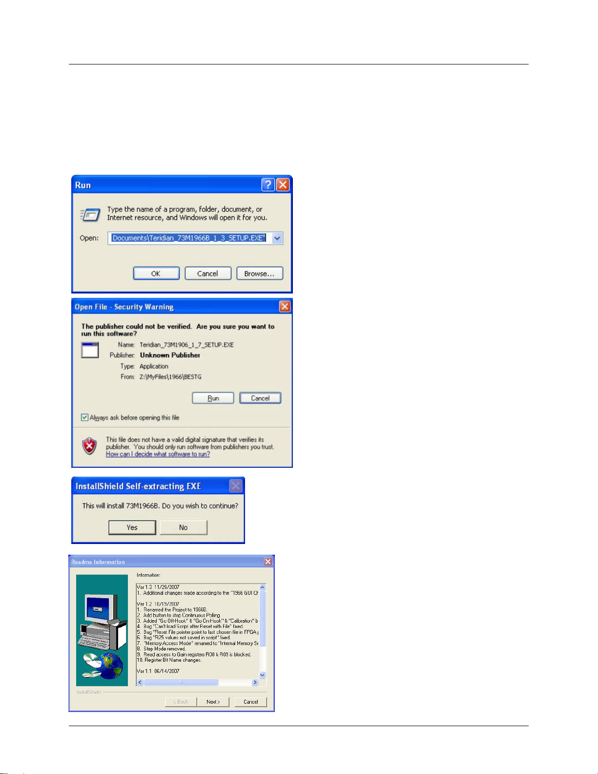
If the GUI software does not r un autom atically when the
CD is installed, select Start Run and browse the CD
drive for Teridian_73M1966_1_3_SETUP.EXE.
Select OK. The followin g window appear s.
Select Ru n.
Select Yes to continue.
The following window appears.
This window lists the revisions of the GUI software
and the improvements mad e in each r evision.
Select N ext . The following window appears.
6 Rev. 1.1
Page 7

UG_1x66B_002 73M1866B/73M1966B GUI U ser Guide
This window shows the default destination for the GUI
software
Select Next. The fol lowing window appears.
The use r can chang e the destination fold er from the
defaul t. C hange the destination folder or select Next to
accept the defaul t folder . Th e GUI software load s into
the specified folder and the following window appears.
The setup is complet e. Click Fini sh. The so ftware is
ready for use.
Rev. 1.1 7
Page 8

73M1866B/73M1966B GUI User Guide UG_1x66B_002
2.2 Using the GUI
The 73M1866B or 73M196 6B Demo Board must be set up before using the GUI. See t he
73M1866B/73M1966B Demo Board User Manual for setup procedures.
To start the GUI using Windows XP , select Start All Pr ograms Teridian Ter idian 73M 1966B.
The Regi ster Access screen appears (see Figure 1). The screen is divid ed into a top half an d a bottom
half. The first row of the top half consists of five t abs: R00-R09, R0A-R12, R13-R1 B, R1C -R25 and FPGA.
The R00-R09 tab displays the regist er map for the first ten 73M1966 B registers. The contents of each
named bit can be changed by checking or un-checking the box n ext to it. A checked box means that the
bit is set to 1 and an un-checked box means th at the bit i s se t to 0. As boxes ar e checked and
un checked, the values i n the bottom hal f reflect the ch anges and turn red. Select new values by checkin g
and un-checking register bits. Click the Write Red but ton to se t the values. N otice that after writing the
values, all previously red values turn black. Polling can be done b y double clicking on the lower regi ster
map for the register you ar e int er ested in or using the “Read All ” r adio butt on.
Figure 1: Register Access Screen – R00-R09 Tab
8 Rev. 1.1
Page 9

UG_1x66B_002 73M1866B/73M1966B GUI U ser Guide
chain, ignoring their individual addresses. When
returns the content of the register corresponding
The bottom half of the Register Access screen shows the status of th e enti r e 73M1x66B r egister set (in
hex) and pr ovides informat i on an d parameter co ntrols.
Table 1 descr ibes these con trols.
Table 1: GUI Contro ls
Click Write Red t o write all red values in the
bottom hal f of the screen. Values become red
Select BR C T (BroadC asT) t o send the same
when chan ged by checking or un-checking boxes
in the top half of the screen . Click Write all to
write al l values (b oth r ead and black). After
writin g values, all values become black an d
remain b l ack un til another box is checked.
Click to read all current valu es from the board.
control d ata to all th e 73M1966B s in a daisy
using the 73M1966B in daisy chain mode, it is
necessar y to set the address of the 73M1966B
that is bei ng acce ssed . Each boar d has a
73M1906B and FPGA address. For exampl e,
the next downst r eam daisy chained 73M 1966B
board will have an address for its 73M1906B of
03h and it s FPGA address will be 04h, and so
on. See Section 5 of the 73M1866/73M1966
Data Sheet for a descripti on of the con trol byte
and the BRCT bit. The radio buttons allow the
selection of 8-bit or 16-bit SPI operations.
Implements the POLL function as described in
Section 6.1 of the 73M1866B/73M1966B Data
Sheet. The Index field corresponds t o the INDX
field (Register 0x19[3:0]). The Value field
corresponds to th e POLVAL field ( Register
0x1F[7:0]). Index is the offset address of the
register t o be manuall y polled with the resu lts
place d in POLVAL. The Index valu e r anges from
0 to 6 only. Index 0 refers to Register 0x12,
Index 1 to Register 0x13, etc. The Value field
Rev. 1.1 9
to the specified Index. Enter the ind ex in the
Index box. Select Poll. When this r egister is
polled, the value is read back in the V al ue box.
After select ing Poll , a red dot next to Match
means that the register was not properly written.
A g r een dot proves that the register was pr operly
written.
Sets the registers to a defaul t oper atin g
configur ation . This i s not t he same as the default
register setting s after t he 73M 1x66 goes thr ough
a device reset. The default register settings may
not be appr opriate for all PCM test sets, so you
may define your own default operating
conditions.
Page 10

73M1866B/73M1966B GUI User Guide UG_1x66B_002
Sets the registers to a user-defined configuration
Register Accesses to File.
Goes On-Hook.
contained in a specified script file. This is used to
qu i ckly p ut the registers into a co nfig urat i on and
the 73M1 x66 into oper ation al mode without having
to individually set t he reg ister bit s. If you have a
configur ation that you will use ag ain later, the
configur ation can be saved as a scri pt. See
Log All
Used to keep a record of all r egister acce sses
performed by the user. Once turned on, user
tran sactions ar e r ecorded in th e file specifi ed in the
window. This is used to record a sequen ce of
operat ions that can be edited and saved as a
script. To use the recorded co nfig uration, see
Reset to Script File.
If Log Status is checked, all SPI transa ctions are
record ed in th e specified fil e, includi ng those
gen er ated by th e backg r ound l ine condit i on
monitori ng routine (line voltag e, current, etc.) . If
Log Status is checked and line con dit ion
monitoring is acti vated, be aware that th e log file i s
continuously increasing in size.
The settin gs for the three most com mon
termination impedance s. These are U.S. (600 Ω),
CTR-21 (complex) and Australian (Australian
complex). Select one to set the termination
impedance. A fter act ivatin g the Read All radio
bu tton, the curr entl y va l id imp edance is indi cated
only if it is one of the three choices. If the currently
valid im pedance is not one of the three choices,
non e of the options will be shown as active.
Goes Off-Hook.
Star ts th e continuous lin e conditi on mon it or i ng
10 Rev. 1.1
Calib r ates t he receive channel of the chipse t.
If the SPI tran sacti ons are corrupted for some
reason, pressing this button resets the 73M1966B
SPI state machi ne and r estores prop er
comm unication between the 73M19 66B and the
GUI.
Updated with the most recen t ring signal voltage as
measured in R1 A. This m easuremen t is only valid
during the on-hook state.
Displays the DC volt age and D C current from the
CO or li ne emulator. Th e current r eading is valid in
off-hook mod e only.
Stops the continu ous line condi tion m onit or ing
rout ine. Line volt age, current, etc. will n ot be
written to the log file.
rout ine. Line volt age, current, etc. will b e written to
the log file.
Page 11

UG_1x66B_002 73M1866B/73M1966B GUI U ser Guide
R03[7:5]
GPIOn
GPIO Pin Enable
7.5
R05[1]
R05[0]
R07[1:0]
DTSTn
Digi tal Test M ode Select
12.7
2.2.1 Controls for Registers R00 to R09
The GUI repr esents 73M 1x66B regi sters i n the form Rhh, where hh i s the hexadecimal address. The
73M1866B/73M1966B Data Sheet repr esents these same registers in th e form 0xhh.
For detailed descriptions of 73M1 x66B registers, see the 73M1866B/73M1966B Data Sheet. Th e tabl es
below list the section numbers in the 73M1866B/73M1966B Data Sheet where additional information can
be found about each bit.
Register Bit Name Summary Description Data Sh e et
Section
R02[7] TMEN Test Mod e Enable 12.7
R02[2] ENLPW
En able L ine Power 9.5
R03[4] PCLKDT PCLK Error Detected 8.8
R03[3] RGMON Ringing Monitor – 0 = silent, 1 = ringing 11.12
R03[2] DET Volt age Det ection – 1 = detection of one of three condi tion s 11.12
R03[1] SYNL Barrier Synchronizat i on L oss has occurred 9.5
R03[0] RGDT Rin g or L ine Reversa l Detection – 1 = a Latched Ring or Line
11.12
Reversal Detecti on e vent
R04[7:5] DIRn GPIO Input/ Ou tp ut Se le ct – 0 = GPIO pin is an output,
7.5
1 = GPIO pin an input
R04[3:0] REVHSDn Host-Side Device Revision 7.1
R05[7:5] ENGPIOn GPIO Enable 7.5
R05[4] ENPCLKDT En able P CL K D etection 8.8
R05[3] ENAPOL Enable Automatic Polling 9.5
R05[2] ENDET En able V oltag e Detection 11.12
ENSYNL Enable Synch Loss Det ection
ENRGDT En able Ring Det ection Interrupt
9.5
11.12
R06[7:5] POLn GPIO Int er r upt Edge Selection 7.5
R08 TXDGn Transmit ter Digital 8.8
R09 RXDGn Recei ver Dig ital Gain 8.8
Rev. 1.1 11
Page 12

73M1866B/73M1966B GUI User Guide UG_1x66B_002
R0D[7]
LOKDET
Ph ase Locked Loop Lock Det ect
7.4
R10[3:2]
CMTXGn
Transmit Path Gain Setting
7.6
R10[1:0]
CMRXGn
Receive Path Gain Setting
7.6
2.2.2 Controls for Registers R0A to R12
Register Bit Name Summary Description Data Sh e et
Section
R0D[6] SLHS Synchronized Lost Host Side 9.5
R0E[7] FRCVCO Force VCO 7.4
R0E[1:0] RGTHn Ring D etect Threshold 11.12
R0F[7] ENFEH Enable Fron t End Host 7.3
R0F[6] PWDN Power Down Mode 7.3
R0F[5] SLEEP Sleep M ode 7.3
R10[4] CMVSEL Call P r ogress Monitor V oltag e Refe r ence Select 7.6
R12[7] OFH Off-Hook Enable 10.6
R12[6] ENDC Enable DC Transconductance Circuit 10.6
R12[5] ENAC Enable AC Transconductance Circuit 10.6
R12[4] ENSHL Enable Shunt Loading 10.6
R12[3] ENLVD LeV Detection (OVDET, UVDET, OIDET monitors)
R12[2] ENFEL Ena bl e Fro nt En d Li ne -Side Circuit
R12[1] ENDT Enab l e Detectors
R12[0] ENNOM Enab l e Nominal Op er ation
10.6
10.6
11.12
10.6
12 Rev. 1.1
Page 13

UG_1x66B_002 73M1866B/73M1966B GUI U ser Guide
R13[0]
SEL16K
Sample R ate Mode Configuration Select
8.8
R14[7]
TXBST
Transmit Boost
8.8
R14[2]
RLPNH
Receive Lo w P ass Not ch
10.6
R15[5]
CHPSEN
En able Chopper Stabilization
10.6
R15[4]
CIDM
Caller ID Mode
11.12
R16[4]
ATEN
Active Termination Loop Enabl e
10.6
R16[3:0]
ACZn
Active Termination Loop s
10.6
2.2.3 Controls for Registers R13 to R1C
Register Bit Na me Summary Description Data Sh e et
Section
R13[7:6] DCIVn DC Cu r r ent Voltage Charact er i stic Control 10.6
R13[5] ILM Current Limit Ena bl e – 0 = no limit, 1 = 42 mA current limit 10.6
R13[4] ACCEN AC Cancellation Enable 10.6
R13[3] PLDM Pulse Dialing Enable 10.6
R13[2] OVDTH Over-Voltage Threshold 11.12
R13[1] IDISPD Discharge and Pulse Dialing 10.6
R14[6:5] DAAn Data Access Arr ang ement
8.8
Used with TXBST to man age tr ansmi t level.
R14[3] RXBST Received Boost
8.8
If set to 1, receive si gn al is increased by 20 dB.
0 = S elects Receive Low Pass Notch (R LPN) at 12 kHz.
1 = S elects RLPN at 16 kHz.
R14[1:0] RXGn R eceive G ain Control 8.8
R15[7] ENOLD Enable Over-Load Detect or 11.12
R15[6] DISNTR Disable No-Tr ansition Timer 11.12
R15[3] THEN Enable Transhybrid Circuit 10.6
R15[2] ENUVD En able Under Vol tage D etect or 11.12
R15[1] ENOVD Enable Over-Voltage Detector 11.12
R15[0] ENOID Enable Over-Curren t Detector 11.12
R16[7] TXEN Tra nsm it Pa th Enable 8.8
R16[6] RXEN Receive Path Enable 8.8
R16[5] RLPNEN Receive Low Pass Notch En able 10.6
R17[5] RXOCEN Rx DC Offset Calibrate Enable 8.8
R18[7:4] TESTn Enabl e Loopback Mode 12.7
R19[7] POLL Polling Enable 6.1
Rev. 1.1 13
Page 14

73M1866B/73M1966B GUI User Guide UG_1x66B_002
Register
Bit Name
Summary Description
Data Sh e et
R19[3:0]
INDXn
Index
6.1
Section
R19[6] MATCH Polling Match 6.1
R19[4] IDL2 Ring Detect Functions 7.3
Add r ess of the register to be manu ally polled with the results
placed in POLVA L.
R1A[7:0] RNGn Result of Au xil iary A /D measur ing t he attenuated ri ng voltage. 11.12
R1B[7:1] LVn Line Voltage Reading 11.12
14 Rev. 1.1
Page 15

UG_1x66B_002 73M1866B/73M1966B GUI U ser Guide
Registers
Description
Data Sh e et
R1E[3]
OLDET
Over-Load Detector
11.12
R23[5:2]
PCODEn
PCM Clock Code
8.8
2.2.4 Controls for Registers R1D to R23
Section
R1C[7:1] LCn Loop Current 11.12
R1D[7:4] REVLSDn Line-Side Device Revision 7.1
R1E[7] ILMON Current Limit Mode On 10.6
R1E[6] UVDET Under-Voltage D etect or 11.12
R1E[5] OVDET Over-V olt age Det ector 11.12
R1E[4] OIDET Over-Current ( I) Det ector 11.12
R1E[2] SLLS Synchro ni za t i o n Loss Li ne Si de 9.5
R1F[7:0] POLLVALn Polling Value
6.1
When poll ed, the con tent of t he Line-Side Device Register
R20[7] TPOL T ransmit Polarity 8.8
R20[6:0] TTSn Transmit Time Slot 8.8
R21[7] RPOL Receive Polarity 8.8
R21[6:0] RTSn Receive Time Slot 8.8
R22[7] SR Samplin g Rat e M ode 8.8
R22[6] ADJ Adjace nt Time Slots 8.8
R22[5:3] RCSn R eceive Clock Slot 8.8
R22[2:0] TCSn Transmit Clock Slot 8.8
R23[7] PCMEN PCM Transmit Enable 8.8
R23[6] MASTER Master/Sla ve Mode
8.8
0 = enables Slave Mode; 1 = enables Master Mode.
R23[1] LIN Linear Mode Enable 8.8
R23[0] LAW Law Compression Mode
R24[0] LB En ables PCM Loopback with in th e H ost-Side Device. 12.7
Rev. 1.1 15
8.8
0 = selects A-law; 1 = selects μ-law.
Page 16

73M1866B/73M1966B GUI User Guide UG_1x66B_002
3 Scripts
If you h ave a con fi gur ation that will b e used again lat er , the configuration can be saved by simple saving
the current configuration by selecting “Save As Scrip t” from the “File” drop-down menu. This will save
ALL the regi ster status informat i on. Once the file has been saved, it can be edited so t hat only the
registers you are i nter ested in changing are contained in t he file. The “Save A s Scr ipt ” function will save
everything in cluding all the read only registers.
Scri pts can b e used to set up any static state you wish, but are lim i ted to just setting the registers. There
is n ot a pr ovision to do delays between the seq uences of reg ister sett i ngs. You cannot, for instance,
pulse dial with a script. Usually this should not be a si gnifica nt l i mitation since normall y only one static
configuration is used at a time. To load a saved configurat i on, select the button under the R eset radio
bu tton or Load Script from the File menu and select th e fi l e that you want to load.
The CD contains sample scripts that can be used to quickly configure the board for specific purposes.
This is a listing of the “setup-wg-init_ofh.tsf” file. Everything necessary for operation is included in this
script.
' 73M1966B Test Script File - setup-wg-init _ofh.tsf
' This script initializes the the 1966 registers
' after a hardware reset. It selects time slot 0
' operation. Make sure hardware reset is performed
' first! The 1966 will go off hook when executed.
'
' Script Format (All Values in Hex)
' Write Register: W,Mode,BRCT,CID,Address,Data
' Read Register: R,Mode,CID,Address,Data
' Mode: 0=8-Bit, 1=16-Bit
' BRCT: Only used in Write
' CID, Address, Data: Hex Value
'
‘ GPIO5-7 inputs set high
W,1,0,0,3,E0
' GPIO5-7 =receivers
W,1,0,0,4,E4
' Enable detectors, polling ID
W,1,0,0,5,1B
' Enable line side device
W,1,0,0,F,80
' Enable OFH, DC, AC, FE, ENNOM
W,1,0,0,12,E5
' Set DCIV=10
W,1,0,0,13,80
' Set DAA=01, RXG=10
W,1,0,0,14,22
' Enable THEN
W,1,0,0,15,08
' Enable TXEN, RXEN, ATEN
W,1,0,0,16,D0
' Set DX polarity, timeslot 0
W,1,0,0,20,9F
' Set DR polarity, timeslot 0
W,1,0,0,21,1F
' Set clock slot for timeslot 0
W,1,0,0,22,3F
' Enable PCM
W,1,0,0,23,80
16 Rev. 1.1
Page 17

UG_1x66B_002 73M1866B/73M1966B GUI U ser Guide
This is a listing of th e “ring-rev-set-up.tsf” file:
' Script - ring-rev-set-up (ON hook)
' This script is used to enable the ring/line reversal
' detection or to go ON hook, no CID
' The time slot is not affected and will remain as
' previously programmed
' Script Format (All Values in Hex)
' Write Register: W,Mode,BRCT,CID,Address,Data
' Write: W, Read: R
' Mode: 0=8-Bit, 1=16-Bit
' BRCT: Broadcast only used in Write
' Chip ID, Address, Data: Hex Value
‘
' Enable detectors, polling ID bits
W,1,0,0,5,13
' Set ring signal threshold to 15V
W,1,0,0,E,01
' Enable barrier interface
W,1,0,0,F,80
' Enable line side device analog ckts
W,1,0,0,12,04
' All off hook functions disabled
W,1,0,0,15,00
' All off hook functions disabled
W,1,0,0,16,00
Note t hat the time slot is not being prog r am med in this case. This still would need to be done at some
point, but it is not nece ssary to have a t ime slot se l ected if the PCM data i s not being sent an d r eceived.
There may also be cases where a specific time slot is bein g used other than t ime slot 0, so i t wou l d not be
desi r able t o change to time slot ze r o every t ime the 73M1966B has a software reset.
In the follo wing prog r am example Cal l er ID can be r eceived so the PC M receive channel must be
configur ed. If the time slot is n ot progr am med it will not be possible to receive th e PCM data when the
Caller ID sign al is sent. It is not, however, necessary to program the PCMEN bit in register 23h since that
is only required to send PCM . The receive analog channel must be turned on for the Caller ID p ath to be
available, so t he RX EN bit in reg i ster 16h must also be turned on. It was not really necessary to program
the tran smit channel time slot at this t ime, but it was done anyway so it won ’ t need to be done separately
later.
' Script - ring-rev-CID-set-up (ON hook)
' This script is used to enable the ring/line reversal
' detection and Caller ID reception
' Script Format (All Values in Hex)
' Write Register: W,Mode,BRCT,CID,Address,Data
' Write: W, Read: R
' Mode: 0=8-Bit, 1=16-Bit
' BRCT: Broadcast only used in Write
' Chip ID, Address, Data: Hex Value
'
' Enable detectors, polling ID bits
W,1,0,0,5,13
' Set ring signal threshold to 15V
W,1,0,0,E,01
' Enable barrier device interface
W,1,0,0,F,80
' Enable line side device analog ckts
W,1,0,0,12,04
' 20dB boost on for CID
W,1,0,0,14,08
' All off hook functions disabled; CID enabled
W,1,0,0,15,30
Rev. 1.1 17
Page 18

73M1866B/73M1966B GUI User Guide UG_1x66B_002
1.1
3/23/2009
Re-wrote Secti o n 3, Scr i pt s .
' Disable off hook functions except RXEN for CID
W,1,0,0,16,40
' Set DX polarity, timeslot 0 of WG
W,1,0,0,20,9F
' Set DR polarity, timeslot 0 of WG
W,1,0,0,21,1F
' Set clock slot for timeslot 0 of WG
W,1,0,0,22,3F
4 Related Documentation
The follo wing 73M1x66B docu men ts are available from Teridian Sem i conduct or C orp or ation :
73M1866B/73M1966B Data Sheet
73M1966B Evaluation Kit User Manual
73M1866/73M1966B Demo Board User Manual
73M1866/73M1966B Keychain Demo Board User Manual
73M1966 Layout Gui del ines
73M1x66B Worldwide Design Guide
5 Contact Information
For m or e i nformation about Ter idian Semicondu ct or prod ucts or to check the availability of the 73M 1866B
or 73M1966B, contact us at:
644 0 Oak Canyon Road
Suite 100
Irvin e, CA 9261 8-5201
Telephone: (714) 508-8800
FAX: (714) 508-8878
Email: modem.support@teridian.com
For a compl ete list of worldwide sales offices, g o to http://www.teridian.com.
Revision Hi story
Revision Date Description
1.0 1/25/2008 First publication.
18 Rev. 1.1
Updated Secti on 4, R el ated D ocumentation.
 Loading...