

Page 1

Simplifying System IntegrationTM
73M1866B/73M1966B
Reference Driver User Guide
June 22, 2009
Rev. 2.7
UG_1x66B_015
Page 2

73 M1 866B/73M1966B Reference Dr iver U ser Guide UG_1x66B_015
© 20 10 Terid i an Semiconductor Corp or ation. All rights reser ved.
Terid i an Semic onductor Corporation is a r egistered trademark of Teridian Semiconductor Corporation.
Simplifying System Integration is a trademark of Teridian Semiconductor Corp or ation.
Linux is a regist er ed tradem ar k of Linus Torvalds.
Asterisk i s a regi stered trademark of Digium, Inc.
All other trademarks are the property of their res pect ive own ers.
Teridian Semiconductor Cor poration makes no warrant y for the use of its products, other than expressl y
contained in the Comp any’s warrant y detailed i n the Teridian Semiconduct or Corporation stan dard Terms
and C ondit ions. The company assumes no responsibility for any errors which may appear in this
document, reserves the right to c hange devices or specific ations detailed herein at any tim e without
notice and does not make any commitment to updat e the i nform ation contained herein . Accord in gly, the
reader is cau tioned to verify that this docum ent i s c urren t by comp ar i ng it to the latest vers ion on
http:// w ww.teridian .com or by checking with your s al es representat i ve.
Teridian Semiconductor Corp., 64 40 Oak Canyon, Sui te 100, I r vine, CA 92618
TEL (714) 508-8800, FAX (714) 508-8877, http://www.teridian.com
2 Rev. 2.7
Page 3

UG_1x66B_015 73M1866B/ 73M196 6B Referen ce Driver Us er Guide
Table of Contents
1
Introduction ................................................................................................................................... 7
1.1 Pu r pose and Scope ................................................................................................................. 7
1.2 Conventions Used in this Guide ............................................................................................... 8
1.3 Acronyms................................................................................................................................. 8
2 Overview ........................................................................................................................................ 9
2.1 Driver Architecture ................................................................................................................... 9
2.2 Functional Overview .............................................................................................................. 10
2.2.1 Event Gen er ation ...................................................................................................... 10
2.2.2 FXO Channel Config and Management ..................................................................... 10
2.2.3 Line State Anal ys i s via Curren t and Voltage Measurements....................................... 10
2.2.4 GPIO Support ............................................................................................................ 11
2.2.5 Loop back and Testing M odes .................................................................................... 12
2.2.6 Call P r ogress M onit or ................................................................................................ 12
2.2.7 Billing Tone Filter....................................................................................................... 12
3 Driver Service Interface ............................................................................................................... 13
3.1 Linux Ope r a t i ng Sy s tem ......................................................................................................... 13
3.2 Other Operating Systems ....................................................................................................... 13
4 Country Specific Se ttings ........................................................................................................... 14
5 FXO Events .................................................................................................................................. 15
5.1 M1966_FXO_EVENT_t .......................................................................................................... 15
5.2 Event Id enti fication................................................................................................................. 16
5.2.1 M1966_BATTERY_DROPPED .................................................................................. 16
5.2.2 M1966_BATTERY_FEEDED ..................................................................................... 16
5.2.3 M1966_ONH_APOH_DETECT.................................................................................. 16
5.2.4 M1966_ONH_NOPOH_DETECT ............................................................................... 17
5.2.5 M1966_ONH_POLARITY_CHG ................................................................................ 17
5.2.6 M1966_OFH_POLARITY_CHG ................................................................................. 17
5.2.7 M1966_RING_DETECT_START ............................................................................... 18
5.2.8 M1966_RING_DETECT_END ................................................................................... 18
5.2.9 M1966_DEVICE_FAILURE_DETECT........................................................................ 18
5.2.10 M1966_OV_DETECT ................................................................................................ 19
5.2.11 M1966_OI_DETECT ................................................................................................. 19
5.2.12 M1966_OL_DETECT ................................................................................................ 19
5.2.13 M1966_LINE_STATE ................................................................................................ 20
5.2.14 M1966_DIAL_COMPLETE ........................................................................................ 20
5.2.15 M1966_DIAL_ABORTED .......................................................................................... 20
5.2.16 M1966_DEVICE_RECOVERED ................................................................................ 21
5.2.17 M1966_GPIO_INTERRUPT ...................................................................................... 21
5.2.18 M1966_ONH_DETECT ............................................................................................. 21
6 IOCTL Commands Description ................................................................................................... 22
6.1 Initialization and Configu ration IOCTLs................................................................................... 23
6.1.1 M1966_CH_INIT ....................................................................................................... 24
6.1.2 M1966_PCM_IF_CSET_OPMODE_SET ................................................................... 25
6.1.3 M1966_PCM_IF_CSET_FREQUENCY_SET............................................................. 26
6.1.4 M1966_PCM_IF_CSET_RPOL_SET ......................................................................... 27
6.1.5 M1966_PCM_IF_CSET_TPOL_SET ......................................................................... 27
6.1.6 M1966_PCM_IF_CSET_RCS_SET ........................................................................... 28
6.1.7 M1966_PCM_IF_CSET_TCS_SET ........................................................................... 28
6.1.8 M1966_PCM_CSET_TSLOT_RX_SET ..................................................................... 29
6.1.9 M1966_PCM_CSET_TSLOT_TX_SET ...................................................................... 29
6.1.10 M1966_PCM_CSET_COMPRESSION_SET ............................................................. 30
6.1.11 M1966_PCM_ACTIVATION_SET .............................................................................. 30
Rev. 2.7 3
Page 4

73 M1 866B/73M1966B Reference Dr iver U ser Guide UG_1x66B_015
6.1.12 M1966_PCM_ACTIVATION_CLEAR ......................................................................... 31
6.1.13 M1966_PCM_ACTIVATION_GET ............................................................................. 31
6.1.14 M1966_CNTRY_NMBR_GET .................................................................................... 32
6.1.15 M1966_GET_COUNTRY_CONFIG ........................................................................... 33
6.1.16 M1966_SET_COUNTRY_CONFIG............................................................................ 34
6.1.17 M1966_PHONE_VOLUME_SET ............................................................................... 35
6.1.18 M1966_PERF_RX_OFFSET_CALIB ......................................................................... 36
6.1.19 M1966_CLEAR_RX_OFFSET_REG ......................................................................... 37
6.1.20 M1966_SAMPLE_RATE............................................................................................ 38
6.2 Events and Status Ser vice ..................................................................................................... 39
6.2.1 M1966_RNG_GET .................................................................................................... 39
6.2.2 M1966_POL_GET ..................................................................................................... 40
6.2.3 M1966_BAT_GET ..................................................................................................... 41
6.2.4 M1966_POH_GET .................................................................................................... 42
6.2.5 M1966_EVENT_GET ................................................................................................ 43
6.2.6 M1966_ERROR_CODE_GET ................................................................................... 44
6.3 FXO Hook S witch Cont r ol Services ........................................................................................ 45
6.3.1 M1966_ENNOM_DELAY_TIMER .............................................................................. 45
6.3.2 M1966_ATH1 ............................................................................................................ 46
6.3.3 M1966_ATH0 ............................................................................................................ 47
6.3.4 M1966_ATDP ............................................................................................................ 48
6.3.5 M1966_ATDP_CANCEL............................................................................................ 49
6.3.6 M1966_ATDP_PARAM ............................................................................................. 50
6.3.7 M1966_FLSH_CFG ................................................................................................... 51
6.3.8 M1966_FLSH_SET ................................................................................................... 51
6.3.9 M1966_SEND_WETTING_PULSE ............................................................................ 52
6.4 Caller-ID S er vices .................................................................................................................. 53
6.4.1 M1966_ENABLE_CALLER_ID .................................................................................. 53
6.4.2 M1966_DISABLE_CALLER_ID ................................................................................. 54
6.4.3 M1966_ENTER_CID_MODE ..................................................................................... 55
6.4.4 M1966_EXIT_CID_MODE ......................................................................................... 56
6.5 Ring Detection Services ......................................................................................................... 57
6.5.1 M1966_SET_MIN_INTER_RING_GAP ...................................................................... 57
6.5.2 M1966_SET_RING_MIN_FREQ ................................................................................ 58
6.5.3 M1966_SET_RING_MAX_FREQ............................................................................... 59
6.6 Line State Anal ys i s Services .................................................................................................. 60
6.6.1 M1966_MEASURE_START ...................................................................................... 60
6.6.2 M1966_MEASURE_STOP ........................................................................................ 61
6.6.3 M1966_MEASURE_UPDATE .................................................................................... 62
6.7 GPIO Services ....................................................................................................................... 64
6.7.1 M1966_GPIO_CONFIG ............................................................................................. 64
6.7.2 M1966_GPIO_CONTROL ......................................................................................... 64
6.7.3 M1966_GPIO_DATA ................................................................................................. 65
6.8 Loop back Services................................................................................................................. 66
6.8.1 M1966_LOOPBACK .................................................................................................. 66
6.9 Miscellaneous ........................................................................................................................ 67
6.9.1 M1966_THRESHOLD_OVERRIDE ........................................................................... 67
6.9.2 M1966_BTONE_FILTER ........................................................................................... 68
6.9.3 M1966_CPROG_MONITOR ...................................................................................... 69
6.9.4 M1966_DEBUG_LEVEL_SET ................................................................................... 70
6.9.5 M1966_TEST_CODE ................................................................................................ 71
7 Type an d St ru ct ure Defin it i on R ef er ence ................................................................................... 72
7.1 M1966_COUNTRY_CODE .................................................................................................... 72
7.2 M1966_CNTRY_STRUCT_t................................................................................................... 74
7.3 M1966_DEBUG_TRACE_MASK............................................................................................ 75
7.4 M1966_LAST_ERROR_CODE .............................................................................................. 75
7.5 struct tx rx_gain ...................................................................................................................... 76
4 Rev. 2.7
Page 5

UG_1x66B_015 73M1866B/ 73M196 6B Referen ce Driver Us er Guide
7.6 M1966_PULSE_DIAL_t ......................................................................................................... 76
7.7 M1966_PULSE_DIAL_PARAM_t ........................................................................................... 77
7.8 M1966_THRESH_OVERRIDE_t ............................................................................................ 77
7.9 M1966_SAMPLE_RATE_SELECTION................................................................................... 78
7.10 Billi ng Tone Filter Related Data Typ e and Structu r e ............................................................... 78
7.10.1 M1966_BTONE_FILTER_COMMAND ....................................................................... 78
7.10.2 M1966_BTONE_FREQUENCY ................................................................................. 79
7.10.3 M1966_BTONE_FILTER_t ........................................................................................ 79
7.11 Call P rog ress Mon itor Data Type and St r uctu r e ...................................................................... 80
7.11.1 M1966_CPROG_MON_VOLT_REF .......................................................................... 80
7.11.2 M1966_CPROG_MON_GAIN .................................................................................... 80
7.11.3 M1966_CPROG_MONITOR_t ................................................................................... 81
7.12 GPIO Related Data Type and St ru ctures ................................................................................ 82
7.12.1 M1966_GPIO_NUMBER ........................................................................................... 82
7.12.2 M1966_GPIO_CONFIG_COMMAND......................................................................... 82
7.12.3 M1966_GPIO_CONTROL_TYPE .............................................................................. 83
7.12.4 M1966_GPIO_DATA_COMMAND ............................................................................. 83
7.12.5 M1966_GPIO_DATA_TYPE ...................................................................................... 84
7.12.6 M1966_GPIO_SIGNAL_DIRECTION......................................................................... 84
7.12.7 M1966_GPIO_INTR_POLARITY ............................................................................... 85
7.12.8 M1966_GPIO_CONFIG_t .......................................................................................... 85
7.12.9 M1966_GPIO_DATA_t .............................................................................................. 86
7.12.10 M1966_GPIO_CONTROL_t ...................................................................................... 86
7.13 Loopback R elated D ata Type and Struc ture ........................................................................... 87
7.13.1 M1966_LOOPBACK_COMMAND.............................................................................. 87
7.13.2 M1966_LOOPBACK_MODE ..................................................................................... 87
7.13.3 M1966_LOOPBACK_t ............................................................................................... 88
7.14 Line Measu r emen t Relat ed Data Types and St r uctures .......................................................... 88
7.14.1 M1966_MEASURE_ENTITY ..................................................................................... 88
7.14.2 M1966_MEASURE_ACTION ..................................................................................... 89
7.14.3 M1966_MEASURE_START_STOP_t ........................................................................ 89
7.14.4 M1966_MEASURE_UPDATE_t ................................................................................. 90
7.14.5 M1966_IET_t............................................................................................................. 91
8 Porting to a Specific H/W Platform ............................................................................................. 92
8.1 Driver Source and Includ e Files.............................................................................................. 92
8.2 Compile Time Configur able P ar ameter s ................................................................................. 92
8.3 Plat form Dependent Macros .................................................................................................. 93
9 Related Documentation ............................................................................................................... 95
10 Contact Information ..................................................................................................................... 95
Appendix A – Country Codes.............................................................................................................. 96
Revision History .................................................................................................................................. 97
Rev. 2.7 5
Page 6

73 M1 866B/73M1966B Reference Dr iver U ser Guide UG_1x66B_015
Figures
Figure 1: Driver Architecture .................................................................................................................... 7
Figure 2: Driver Function al B lock Diag ram
Figure 3: Loopback Modes
Tables
Table 1: Summary of Initializ ation IOCTLs ............................................................................................. 23
Table 2: FX O Line Status Services
Table 3: FX O Hook Switch Control Services
Table 4: Call ID Services
Table 5: Ring Detecti on Services
Table 6: Li ne State An alysis S er vices
Table 7: Driv er Sour ce Code F iles
Table 8: Cou ntry Code Tab l e
............................................................................................... 9
.................................................................................................................... 12
........................................................................................................ 39
.......................................................................................... 45
....................................................................................................................... 53
........................................................................................................... 57
.................................................................................................... 60
......................................................................................................... 92
................................................................................................................. 96
6 Rev. 2.7
Page 7

UG_1x66B_015 73M1866B/ 73M196 6B Referen ce Driver Us er Guide
1 Introduction
This document describes t he capabilit i es of th e 73M1866B/73M1966B Reference Driver. This driv er
software is provided for use and integration by Teridian customers on their individual platforms. The
intent i on of this Reference Driver is to provide a customizabl e frame work that is independent of p r ocessor
and operating system.
Throughout thi s do c u me nt the 73M1x66B Reference Device driver will b e sim ply referred to as “driver ” or
“device dri ver”. The 73M1866B and 73M196 6B will b e collectively referred to as the 73M1x66B.
1.1 Purpose and Scope
The 73M1x6 6B Referen ce Driver p rovid es the necessary system interfaces for the con trol an d
management of the 73M1x66B. The driver supports API calls from the application and translates these to
and from the device. The driver can be u sed as i s, in whole or in part, or customized to accommodate a
custo me r ’s unique envir o nme nt.
The scope of this document includes discussion of driver’s architecture and design, interface to the user
application, the driver in ternal state machine, and the h ar dware interfac e to the 73M1x66B hardware
device via the S PI bus .
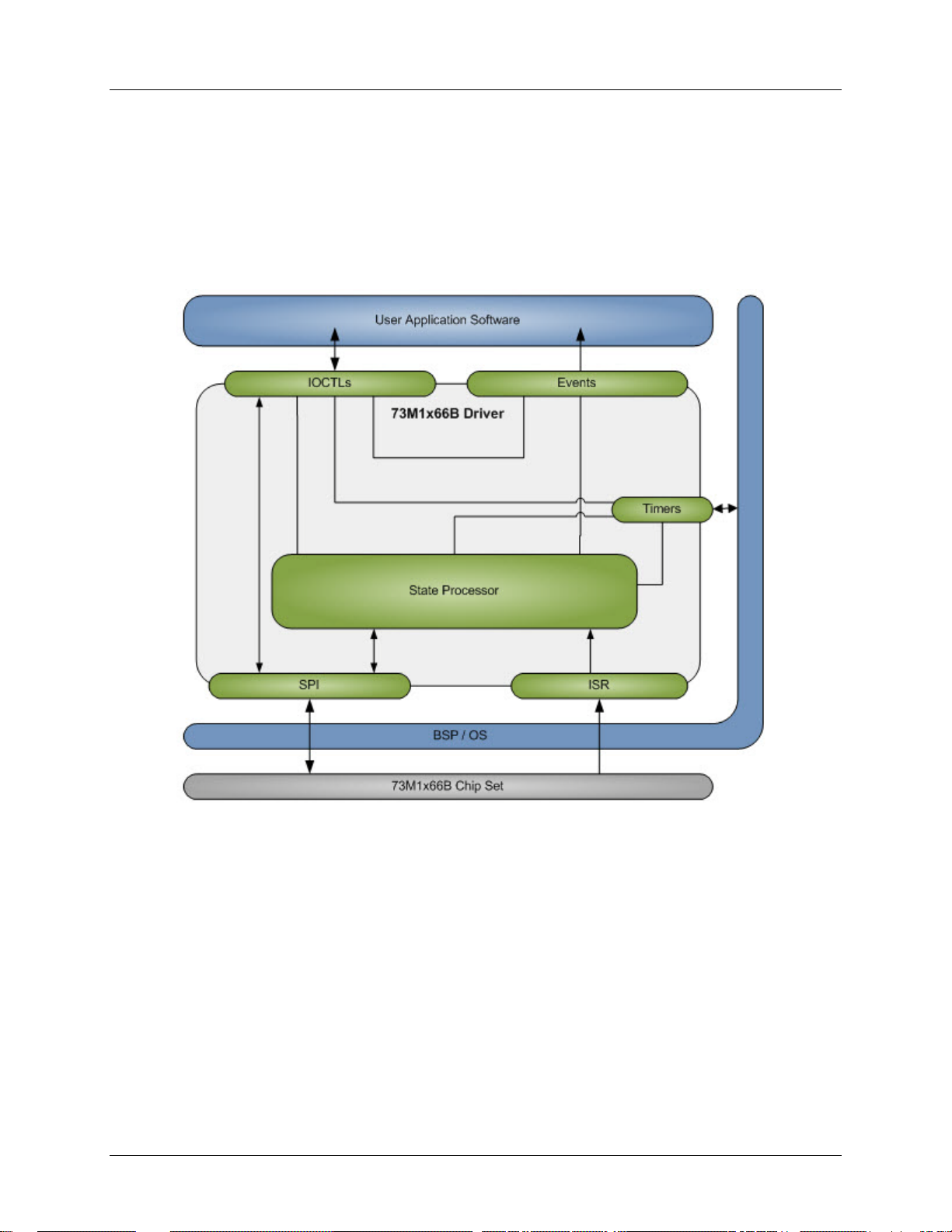
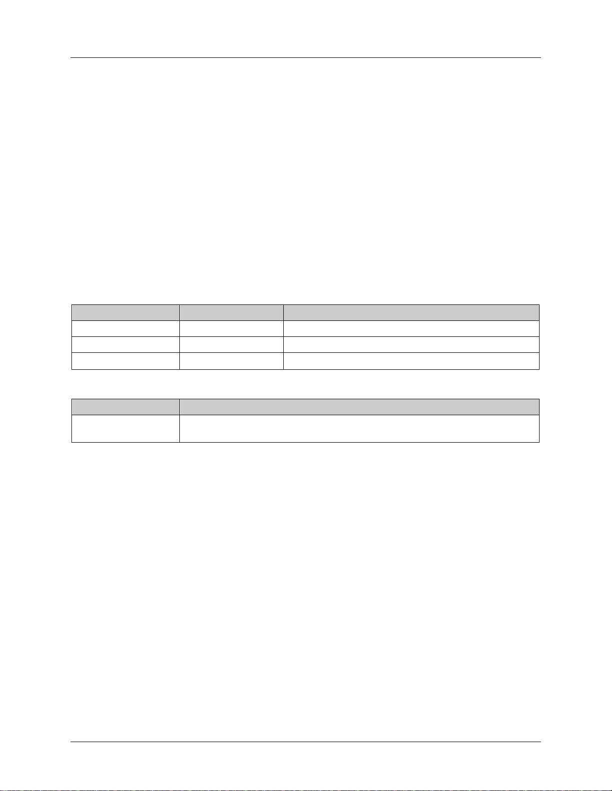
Figure 1 illustrates the bas ic architectu r e m odel for t he dr i ver. The mod el is intended to b e i ndependent
of processor and operati ng system. Layers above t he referen ce driver address software interfaces wh ich
may pre-exist for a given application ( e.g. Aster i sk
interfaces bet ween t he pr ocessor and the 73M1x66B devices.
®
) and the layer b elow addresses hardware related
Figure 1: Driver Architecture
Rev. 2.7 7
Page 8

73 M1 866B/73M1966B Reference Dr iver U ser Guide UG_1x66B_015
1.2 Conventions Used in this Guide
This document uses the following conventions:
• Software code, I OCTL names , F XO events, data t ypes, and Linux c ommands are presen ted i n
Couri er font.
• A table with a blue header i s a summary tab le. A tabl e with a g r ay header i s a det ail table.
1.3 Acronyms
APOH – An other Phone Off Hook
BSP – Board Support Package
DAA – Data A ccess Arran gem ent
FXO – Foreign eXchange Office
ISR – Interrupt Service Routine
IOCTL – I/O Control
NOPOH – N o Phone Off Hook
POH – Phone Off Hook
SPI – Serial Perip heral Int er face
GPIO – General Pu r pose Input/Output
8 Rev. 2.7
Page 9
UG_1x66B_015 73M1866B/ 73M196 6B Referen ce Driver Us er Guide
2 Overview
2.1 Driv er Arc hite ctur e
The dri ver provides a framework by which appli cations can leverage the featu r es of t he chipset . The
main interface o f th e driver (IOCTLs) provides an abstraction layer for monit or i ng and cont r ol of the
device s tatus. Device status is analyzed and pr ocessed by an independently running process based on
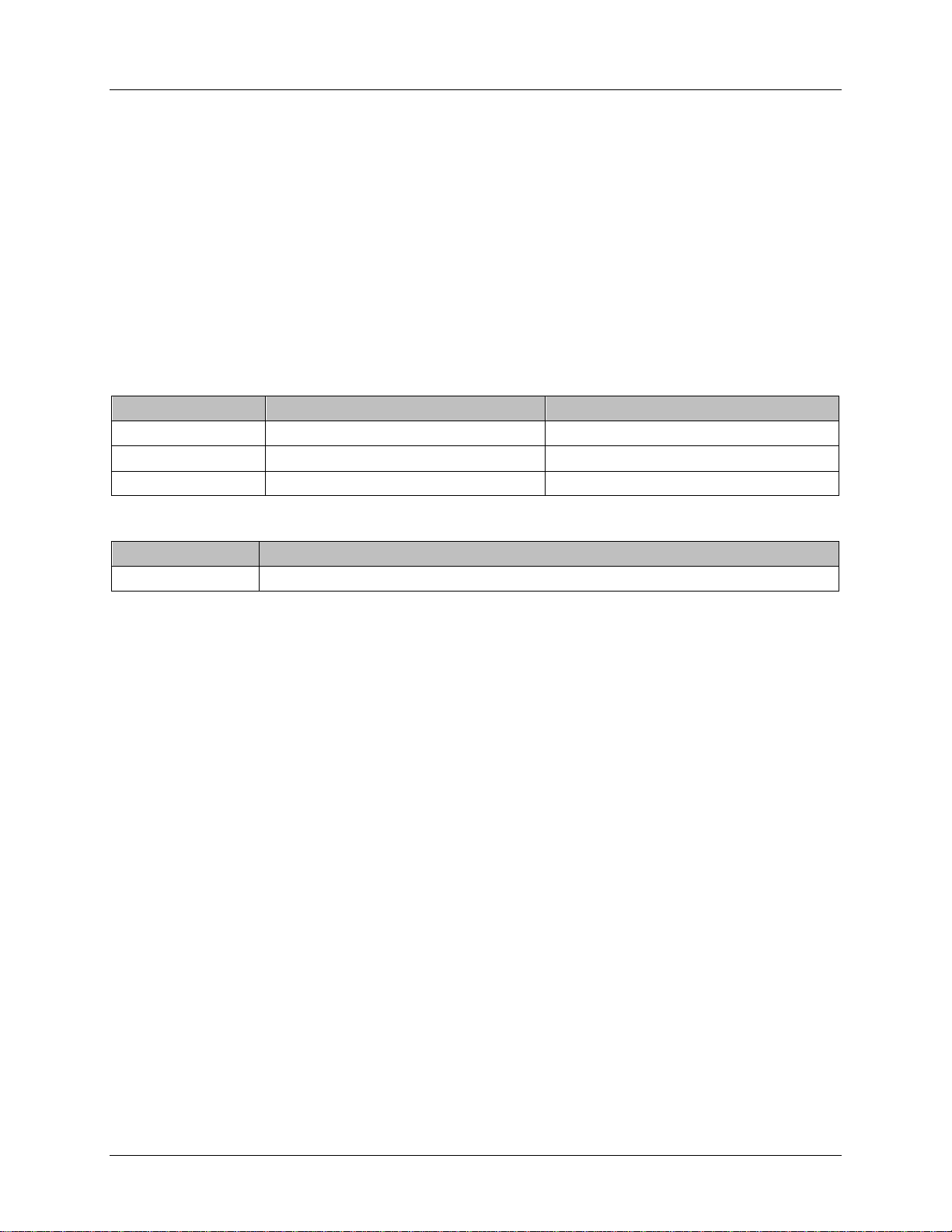
predefined algor i thms. When an event or an even sequence is recog nized, the d r i ver post s th e
correspondin g event to be retrieved by th e user applicati on. Figure 2 depicts the driver functional block
diagram.
Figure 2: Driver Functional Block Diagram
The driver provides an interface to user ap plication th r ough the IOCTL and Events interface. Through this
interface, the user applic ation communicates with the driver via a st andar d device interface (open, close,
select, ioctl functions). Using this interface the appl icati on will b e able t o cont rol the operation of th e
device and to retri eve the status of the FXO line. Section 6 descri bes the det ai ls of th i s interfac e.
The driver provides access to the 73M1x66B device via the SPI bus, and through the interrupt s er vice
routine (ISR) triggered by the hardware interrupt signal. The driver accesses t he platfor m's SPI hardware
interface directly through the system’s board support package (BSP). This access is in the context of an
operat ing system p latform device defini tion .
The 73M1x66B driver is bui lt as a Linux load able module (for Linux) or integrated wi th the operating
system kernel. It will be brought into operation by a user ap plic ation or by an operati ng system startup
script. For Linux, the insmod command is used t o inser t the dri ver i nto the ker nel. The insmod
command invokes the module_init() macro, which in turn runs the one-time initializati on function of
the driver. Before exiting the ini tialization the driver enters its main operational s tate via the scheduli ng of
one of m any timers that make up the driver’s m ain processing.
Rev. 2.7 9
Page 10

73 M1 866B/73M1966B Reference Dr iver U ser Guide UG_1x66B_015
2.2 Functional Overv ie w
Once inst alled, th e dr iver is a self-contained module run ning in dependently along with the kernel
processes. Its main purpose is to monitor the F XO line for various conditions, gen erates appropriated
event when they occur, and t o provide access to the 73M1x66B device for management purposes , via
standard driver access methods such as open, close, select, ioctl, etc . Th e following sections
provide an overview of the functionalities.
2.2.1 Event Generation
During operation the d r i ver constantly monitors th e line for the following conditions:
1. APOH condition.
2. Transition back to no APOH condition (NOPOH).
3. R i ng start detection.
4. End of Ri ng condition.
5. Battery dis connected condition.
6. Battery restored conditi on.
7. Polarity reve r sal condition.
8. Line State condition – monit or ing of voltage and current.
9. Device failure condition.
10. Over voltage, curren t, or l oad condition.
11. Pu l se dial compl ete event .
12. Pulse dial aborted event .
13. Device rec overed even t.
Section 5 provides detail descripti ons of each even t.
If any of these conditions occur the dri ver creates an event ent r y in the event queue and notifies the
app l icati on layer via file descrip tor ready mechanism (or via file descr ipt or select() function). Upon
receiving th is “wakeup” n otification, the application can then test the file d escriptor “ready” status with the
FD_ISSET macro to con fir m, and then retrieve the event from the driver via IOCTL event get command.
2.2.2 FXO Channel Config and Management
Configuration of the FXO parameter s such as PCM parameter and other management command such as
hook switch operation are done via st andar d device driver IOCTLs. The 73M1x66B Referen ce Driv er
provides an extended list of IOCTLs for this purpose. The IOCTL command descriptions in Section 6
provide details of how the y work.
2.2.3 Line State Analysis via Current and Voltage Measurements
The 73M1x66B Reference Driver can be programmed to provide extended line status information and
line monitori ng capabil i ty. The d r iver op er ates autonomously, under the application la yer cont r ol , to detect
line condition specified in pre-set criteria and automatically report status change. This allevi ates t he
bu r den of con stant polli ng from the appl ication layer. The line stat us c onsists of t he line vo ltag e and l ine
curr ent measurements. Each measurement entity is operated independently as descri bed below.
2.2.3.1 Interval and Even Table
The Interval and Event Table (IE T) is a tab le th at con sists of mul tip l e r ows of the following informati on:
1. Row number.
2. Lower bound threshold.
3. Upper bound threshold.
4. Applicati on defined event.
10 Rev. 2.7
Page 11

UG_1x66B_015 73M1866B/ 73M196 6B Referen ce Driver Us er Guide
The application is responsible for building up the IET using the IET table update IOCTL –
M1966_MEASURE_UPDATE. This IOCTL can be used t o create/update or to read back the current table
en try (see Section 6.6.3 for detail s).
2.2.3.2 Measurement Procedure
The dri ver is responsible for readi ng the raw valu e r equi r ed at a given s amp le rate f r om the device. The
result is computed and averaged over a specified number of those pr eviously read values, and then
compare to the i nterval and event table (I ET) des cribed below. Based on these compar isons dedicated
events may be sent to the appl i cation.
The dri ver compares th e calculated averag e of the readi ng value with the l ow er and upper bou nd
thr eshold in each IET table entry. I f the value falls in between the ranges and it is th e fir st t r ansition int o
these new ran ges t he specific appl ication defi ned event (4) will be sent t o the application. Th e lower and
upp er bound rang es are exp r essed i n m illiamps for curren t intensity, or in volts for line voltage.
2.2.3.3 Management of the Procedure
Controlling the operati on of this cur r ent/voltage measurement is exclusively done by the application layer.
The application layer uses the M1966_MEASURE_START and M1966_MEASURE_STOP to start and stop
the measurement, respectively. The M1966_MEASURE_STOP simply stops the measurem ent and
requires no additi onal p ar ameter , while M1966_MEASURE_START starts the measuri ng pr ocess and it
consists of two parameters:
1. Sample t ime interval.
2. Average sample c ount.
The sample tim e i nterval i s the time i nterval between two cons ecut ive read i ng sampl es expressed in
mil l iseconds, and the average sam ple count is the number of reading samples to be us ed for average
calculati on. Any one of these p ar ameter s can be ZE RO indicat es a no change. The ap plic ation l ayer can
adjust one or both par amet er s anyti me using M1966_MEASURE_START.
2.2.3.4 Even Handling
The dri ver emits the M1966_LINE_STATE event when line s tate c ondit i on changes from one interval to
another. The application i s expected t o r eceive t he notification and can reques t for the event from the
driver using the M1966_GET_EVENT IOCTL. Refer to Section 5 for details on how to get notified and to
retrieve t he event from the driver’s queue. The following supporting data will accompany the line st ate
event:
1. Th e stat e of the FXO channel – on or off-hook.
2. Lin e current or line voltag e.
3. IET row index.
4. Applicati on defined event.
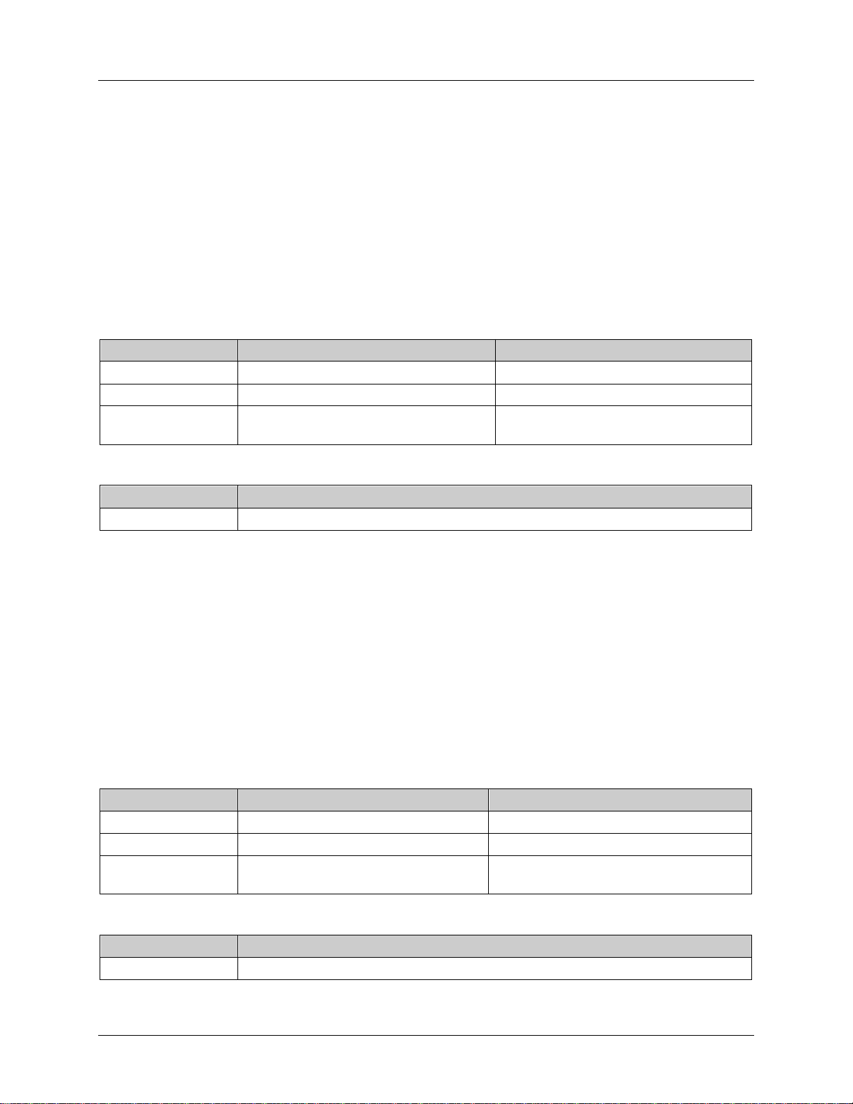
2.2.4 GPIO Support
Three General Purpose I/O pins (GPIOs) pins can be managed independently and used for carrying input
or out put signal to and from the 1906 device. If used as input, signal transition on the pin can be detected
and trigger interrupt to the host CPU. The driver provides the ability to program each GPIO pin as input
or out put port, the ab ility t o r ead and write data t o the GPIO pin as well as generating in terru pt event
correspond the signal transition. Secti on 6.7 describes the GPIO related IOCTL.
Note: The GPIO feature exi sts only on the 73M1906B 32-Pin QFN package.
Rev. 2.7 11
Page 12
73 M1 866B/73M1966B Reference Dr iver U ser Guide UG_1x66B_015
TBS
DSDM
PRM SCM
MSBI
LSBI
RxAFE
SinC3
Filter
Onchip
LIC
SPI
Interface
PCM
Interface
TxAFE
Interp.
Filter
Decim.
Filter
TxData
RxData
RBS
Tip
Ring
PRP SCP
TxD
RxD
CTL
STA
External
LIC
73M1906B
73M1916
Aux A/D
STA
ALB
INTLB1
DIGLB2
DIGLB1
INTLB2
RxA
TxA
PCMLB
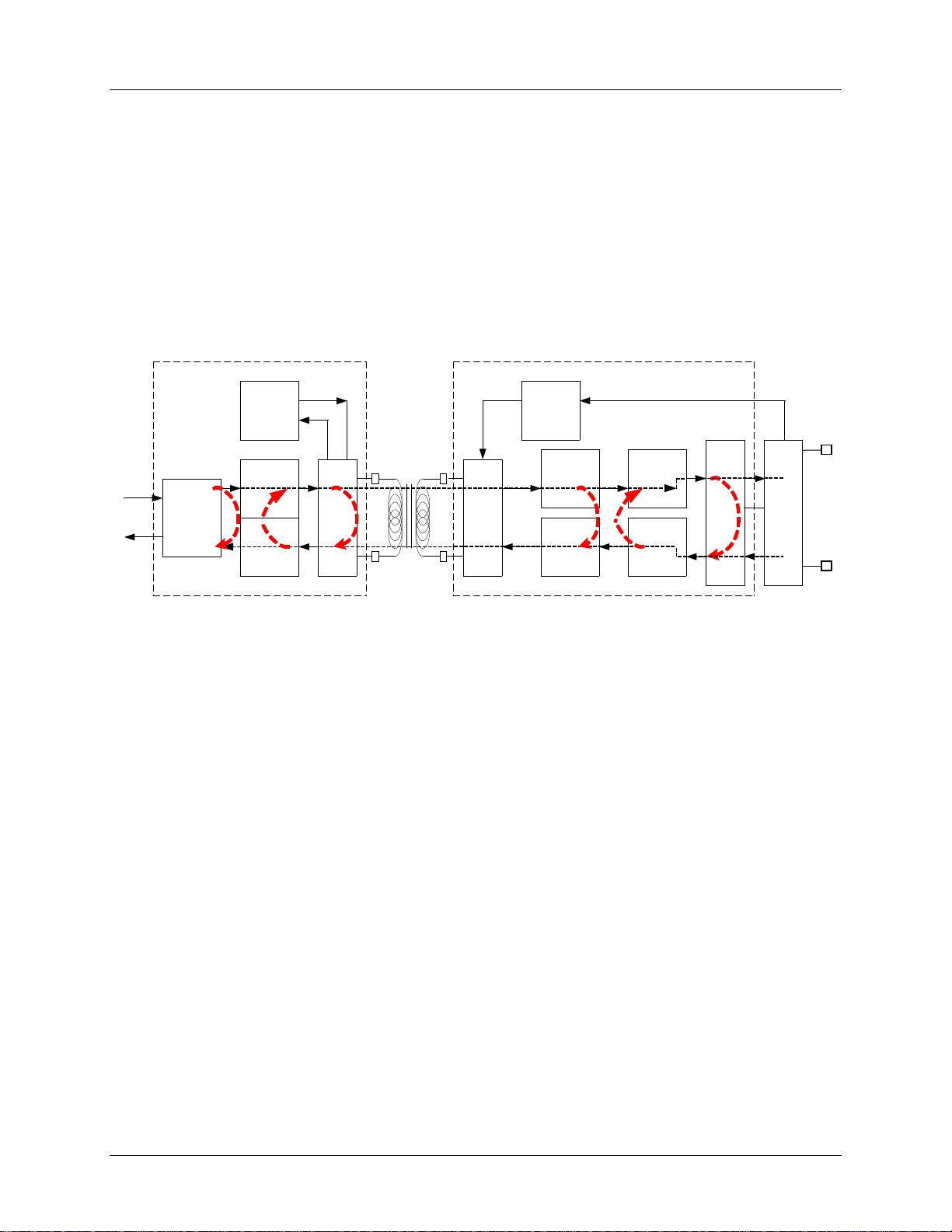
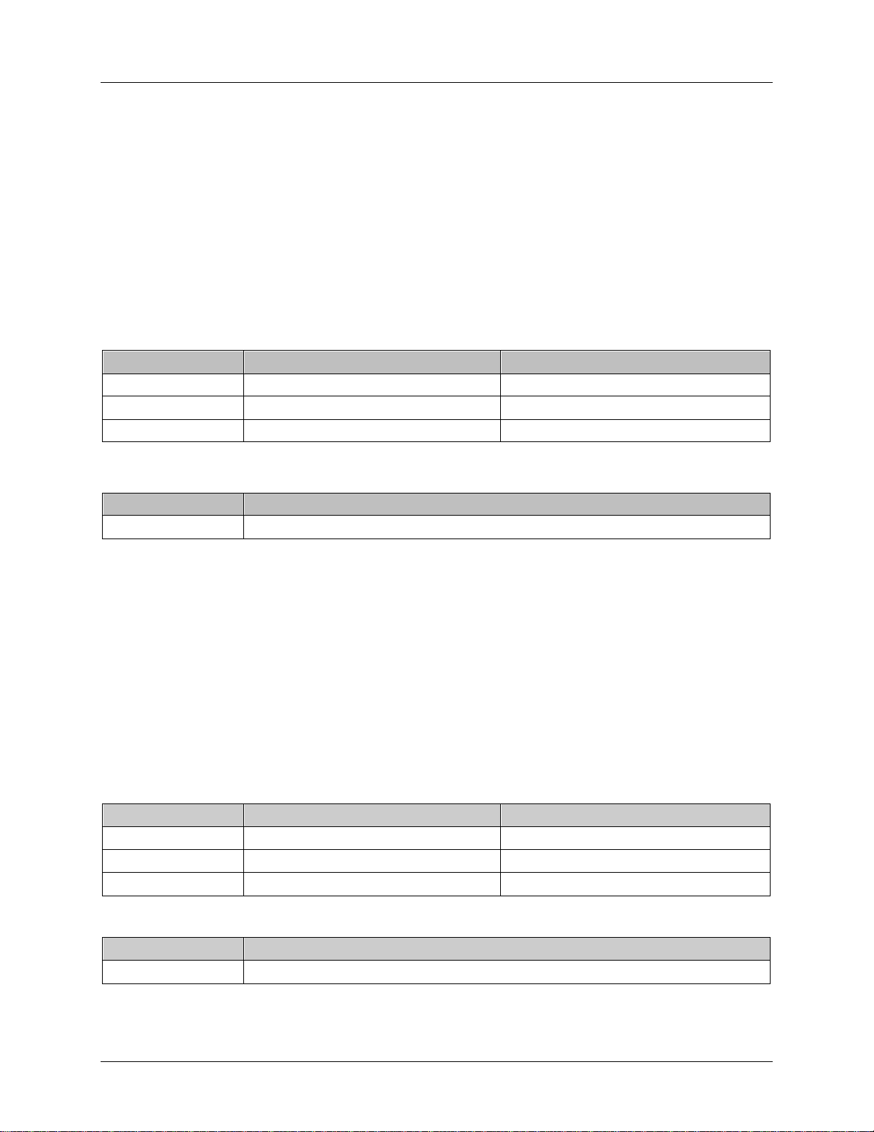
2.2.5 Loopback and Testi ng Mo de s
The 1966B devices support six variations of loopback modes. Refer to the “Loopback and Testing
Modes” secti on of the 73M1866B/73M1966B Data Sheet for mor e detai l . Each loopback mod e i s
desi gned to test connectivity at variou s points in the system. Systematically use of the loopback feature
in c onjun ction with ext er nal application that c ontrol d ata st r eam in and out of the s ystem can be an
effect ive tool to i solate faults . While the driver provides IOCTLs to manage those loopbac k test points, i t
does not have a way to i nject or in tercept d ata flow throu gh the syst em to perform d iagnostic. It reli es on
external ap plic ation for those capabilities. The IOCTL for managing the l oopback can be foun d in Section
6.8.1
Figure 3 shows the si x different loopback m odes.
Figure 3: Loopback Modes
2.2.6 Call Progress Monitor
The 1966B device provides th e ability to monitor act i vity on the l i ne via feature c alled the Call Progress
Monitor. The gain setting of its au dio path can be adjusted using the M1966_CPROG_MONITOR IOCTL
detailed in Sectio n 6.9.3. For more detail on this subj ect, refer to the “Call Prog ress Monitor” section of
the 73M1866B/73M1966B Data Sheet.
2.2.7 Billing Tone Filter
Some countries use a large am plitude out-of-ban d tone to measure c al l duration and to allow remote
central offices to determine the durat ion of a call for billing purposes. To a void sat uration and distortion of
the input caus ed by th ese tones, i t is imp or tant t o be able to rejec t them. These frequencies ar e typic ally
12 kHz and 16 kHz. Refer to section “ Billi ng Tone Rejection” in the 73M1866B/73M1966B Data Sheet for
more detail .
To enable or d i sable the billi ng tone filter, the driver offers the M1966_BTONE_FILTER IOCTL. Its
description can be found in Section 6.9.2.
12 Rev. 2.7
Page 13

UG_1x66B_015 73M1866B/ 73M196 6B Referen ce Driver Us er Guide
3 Driver Service Interface
The Driver Ser vice provides the link b etween the FXO device and th e user application. First, the driver
must be load ed and bind ed into the operatin g system environment before this s er vice can be provid ed.
Access to the driver is done via two file descriptors – the device and channel file descriptors. The d evice
file descript or provides access to device level management interface while the channel descriptor is used
to m anage at the ch annel l evel interface. The driver supports multiple FXO channels through separated
channel descriptors ; however, only one device descr ipt or i s us ed.
The following sections describe how the driver is brought into action based on the operating system
environment.
3.1 Linux Operating System
This description is valid for Linux 2.4 and 2.6. The 73M1x66B driver takes the form of a Linux standard
character device driv er . It is brought into operation by a user ap plic ation or by Linux startup s crip t using
the
insmod command. This command inserts the dr iver module in to the kernel which in turn registers
with the kernel using the default major number of 221. Multiple FXO channels are supported via the use
of minor number which can varies from 0 to 16. This minor number associated wit h the device an d
channel descriptors c r eated using mknod command. The driver expects the minor number 0 to be
associ ated with the device descriptor an d the number from 1 to 16 with the channel descriptors. Device
major and minor numbers ar e configurable at bui ld time as desc ribed in Sec tion 8 .2.
The dev i ce and ch annel d escriptors can be created in the /dev directory at th e same time when th e
driver is insmod into the ker nel. The mknod command is used to create t hose descrip tors as illustrated
below:
mknod -m 660 /de v/ter10 c 221 10
mknod -m 660 /de v/ter11 c 221 11
In this example, one device descriptor (ter10) is created with major number 221, minor number 10, and
one channel d escriptor (ter11) is created with m ajor number 221, minor number 11. The min or numb er
base 10 can be changed (see the c om pile time configurabl e parameter in Section 8.2).
Once the driver is installed and the device/channel descriptors are created, the dr i ver service can be
accessed via standard C library
functi ons.
The following illustrates how the device and channel ar e open ed, c losed, and the IOCTL access:
devfd = open("/dev/daa_dev",O_RDONLY|O_WRONLY);
chanfd = open (“/ dev /daa_chan1”, O_RDONLY|O_WRONLY);
ioctl (devfd, M1 966 _EV ENT _GE T, &event_st ruc tur e);
ioctl (chanfd, M1966_ATH1, NULL);
close (devfd);
close (chanfd);
Accessing the driver using IOCTL must be done via an opened descriptor. There are t w o types of IOCTL
commands – the device level commands, which can be accessed by an op ened device descrip tor, and
channel l evel commands, which can be acc essed using an opened channel descriptor. Section 6
describes th e IOCTL commands.
3.2 Other Oper ati ng Systems
open(), and sub sequently with select(), close(), and ioctl()
To be provided.
Rev. 2.7 13
Page 14

73 M1 866B/73M1966B Reference Dr iver U ser Guide UG_1x66B_015
4 Country Specific Settings
The 73M1x66B Reference Dri ver supports gl obal comp l iance par ameter s for each DA A device it
manages. When select ed for a specific country code using M1966_CH_INIT, the following predefined
parameters will be applied:
1. AC ter minat ion impedance – AC impedance register value.
2. DC termination mask – DC mask value.
3. Ring Detection – Ri ng detection threshold value.
4. Automatic CID Enable – Automatic ally enter CID s tate when on hook .
5. U se Seize State – I f s et, the driver enter s eize state for 350 ms before s etting ENNOM (refer to the
73M1x 6 6B Data Sheet, Section 10.2 – DC Terminati on, for the detail explanation of the seize state) .
These p ar ameter s are defined i n the Country Cod e Parameter files (m1966_cntry_tbl.c) and c an be
changed as required. The list of the country codes supported can be found in Appendix A.
14 Rev. 2.7
Page 15
UG_1x66B_015 73M1866B/ 73M196 6B Referen ce Driver Us er Guide
unsigned int
event_id
unsigned int
channel_id
unsigned int
event_cnt
unsigned int
event_data1
unsigned int
event_data2
unsigned int
event_data3
unsigned int
event_data4
5 FXO Events
The dri ver provides event service to the high l evel appl ication by main taining a FIFO queue of even t
structures, M1966_FXO_EVENT_t. Events ar e created by the driver to r eflect various conditions as
described in Section 5.2. Once created, this new e vent is added to the FIFO queue and the driver notifies
the application layer via file descr i ptor stat us change mechanism. This in turn triggers th e application t o
request for the ev ent via the M1966_EVENT_GET IOCTL. Upon retr i eval, eac h event structure is removed
from t he FI FO queu e after its informati on is conveyed to th e hi gh level ap plic ation.
To receive t his F XO event noti fi cation the app licat i on mu st register for file descriptor s tatus change us i ng
the standard UN IX select() function. When this function returns the FXO event availability status will
reflec t in the fil e desc r i ptor parameter. The FD_ISSET macro can be used for checking the status, and if
available, the application c an request for the even t us ing M1966_EVENT_GET.
5.1 M1966_FXO_EVENT_t
Description
Thi s str uct ur e is us e d by M1966_EVENT_GET to retrieve an event from the event queue. The event
structure consists of event ID indentifying the event, the channel ID identifying the FXO channel where
the event was g ener ated, the number of remaining events in the queue, and up t o four event d ata that
carries addi tion al info r mati on per tain i ng to that s pecific even t.
Prototype
typedef struct {
unsigned int event_id; /* Event ID */
unsigned int channel_id; /* Channel ID */
unsigned int event_cnt; /* number of remaining queued events */
unsigned int event_data1; /* additional data 1 */
unsigned int event_data2; /* additional data 2 */
unsigned int event_data3; /* additional data 3 */
unsigned int event_data4; /* additional data 4 */
}
M1966_FXO_EVENT_t;
Parameters
Data T ype Name Description
Event ID (see Section 5.2).
Channel ID.
Number of even ts t hat remain in the queue.
Event dat a 1.
Event dat a 2.
Event dat a 3.
Event dat a 4.
Rev. 2.7 15
Page 16
73 M1 866B/73M1966B Reference Dr iver U ser Guide UG_1x66B_015
unsigned int
event_id
M1966_BATTERY_DROPPED
unsigned int
channel_id
unsigned int
event_cnt
unsigned int
event_data1
unsigned int
event_data2
unsigned int
event_data3
unsigned int
event_data4
unsigned int
event_id
M1966_BATTERY_FEEDED
unsigned int
channel_id
unsigned int
event_cnt
unsigned int
event_data1
unsigned int
event_data2
unsigned int
event_data3
unsigned int
event_data4
unsigned int
event_id
M1966_ONH_APOH_DETECT
unsigned int
channel_id
unsigned int
event_cnt
unsigned int
event_data1
unsigned int
event_data2
unsigned int
event_data3
unsigned int
event_data4
5.2 Event Identification
5.2.1 M1966_BATTERY_DROPPED
This event occurs when the FXO line is disconnected from the telephone network.
Parameters
Data T ype Name Description
.
Channel ID.
Number of even ts t hat remain in the queue.
N/A.
N/A.
N/A.
N/A.
5.2.2 M1966_BATTERY_FEEDED
This event is generated when the line is connected to the telephone network and the vo ltag e is restored
to normal operating level.
Parameters
Data T ype Name Description
.
Channel ID.
Number of even ts t hat remain in the queue.
N/A.
N/A.
N/A.
N/A.
5.2.3 M1966_ONH_APOH_DETECT
This event is generated when a parall el phone goes off hook while the FXO line i s in on-hook state.
Parameters
Data T ype Name Description
.
Channel ID.
Number of even ts t hat remain in the queue.
N/A.
N/A.
N/A.
N/A.
16 Rev. 2.7
Page 17
UG_1x66B_015 73M1866B/ 73M196 6B Referen ce Driver Us er Guide
unsigned int
event_id
M1966_ONH_NOPOH_DETECT
unsigned int
channel_id
unsigned int
event_cnt
unsigned int
event_data1
unsigned int
event_data2
unsigned int
event_data3
unsigned int
event_data4
unsigned int
event_id
M1966_ONH_POLARITY_CHG
unsigned int
channel_id
unsigned int
event_cnt
unsigned int
event_data1
unsigned int
event_data2
unsigned int
event_data3
unsigned int
event_data4
unsigned int
event_id
M1966_OFH_POLARITY_CHG
unsigned int
channel_id
unsigned int
event_cnt
unsigned int
event_data1
unsigned int
event_data2
unsigned int
event_data3
unsigned int
event_data4
5.2.4 M1966_ONH_NOPOH_DETECT
This event i s generated when a parallel phone goes back on hook while the FXO line is in on-hook state.
Parameters
Data T ype Name Description
.
Channel ID.
Number of even ts t hat remain in the queue.
N/A.
N/A.
N/A.
N/A.
5.2.5 M1966_ONH_POLARITY_CHG
This event is gener ated when there is a voltage revers al occurs on the line while in on-hook state.
Parameters
Data T ype Name Description
.
Channel ID.
Number of even ts t hat remain in the queue.
N/A.
N/A.
N/A.
N/A.
5.2.6 M1966_OFH_POLARITY_CHG
This event is gener ated when there is a voltage revers al occurs on the line while in off-hook state.
Parameters
Data T ype Name Description
Rev. 2.7 17
.
Channel ID.
Number of even ts t hat remain in the queue.
N/A.
N/A.
N/A.
N/A.
Page 18
73 M1 866B/73M1966B Reference Dr iver U ser Guide UG_1x66B_015
unsigned int
event_id
M1966_RING_DETECT_START
unsigned int
channel_id
unsigned int
event_cnt
unsigned int
event_data1
unsigned int
event_data2
unsigned int
event_data3
unsigned int
event_data4
unsigned int
event_id
M1966_RING_DETECT_END
unsigned int
channel_id
unsigned int
event_cnt
unsigned int
event_data1
unsigned int
event_data2
unsigned int
event_data3
unsigned int
event_data4
unsigned int
event_id
M1966_DEVICE_FAILURE_DETECT
unsigned int
channel_id
unsigned int
event_cnt
unsigned int
event_data1
unsigned int
event_data2
unsigned int
event_data3
unsigned int
event_data4
5.2.7 M1966_RING_DETECT_START
This event is gener ated at the b eginning of t he ring bur s t .
Parameters
Data T ype Name Description
.
Channel ID.
Number of even ts t hat remain in the queue.
Ring burst frequency (in Hz).
N/A.
N/A.
N/A.
5.2.8 M1966_RING_DETECT_END
This event is gener ated when the driver detects the end of the ring burst.
Parameters
Data T ype Name Description
.
Channel ID.
Number of even ts t hat remain in the queue.
Ring burst frequency (in Hz).
Ring bur st durat ion (in ms).
N/A.
N/A.
5.2.9 M1966_DEVICE_FAILURE_DETECT
This event is generated when th e dr i ver detec ts the device failure.
Parameters
Data T ype Name Description
18 Rev. 2.7
.
Channel ID.
Number of even ts t hat remain in the queue.
N/A.
N/A.
N/A.
N/A.
Page 19

UG_1x66B_015 73M1866B/ 73M196 6B Referen ce Driver Us er Guide
unsigned int
event_id
M1966_OV_DETECT
unsigned int
channel_id
unsigned int
event_cnt
unsigned int
event_data1
unsigned int
event_data2
unsigned int
event_data3
unsigned int
event_data4
unsigned int
event_id
M1966_OI_DETECT
unsigned int
channel_id
unsigned int
event_cnt
unsigned int
event_data1
unsigned int
event_data2
unsigned int
event_data3
unsigned int
event_data4
unsigned int
event_id
M1966_OL_DETECT
unsigned int
channel_id
unsigned int
event_cnt
unsigned int
event_data1
unsigned int
event_data2
unsigned int
event_data3
unsigned int
event_data4
5.2.10 M1966_OV_DETECT
This event is gener ated on detection of an over voltage lin e condition.
Parameters
Data T ype Name Description
.
Channel ID.
Number of even ts t hat remain in the queue.
N/A.
N/A.
N/A.
N/A.
5.2.11 M1966_OI_DETECT
This event is gener ated on detection of an over c urrent line condition.
Parameters
Data T ype Name Description
.
Channel ID.
Number of even ts t hat remain in the queue.
N/A.
N/A.
N/A.
N/A.
5.2.12 M1966_OL_DETECT
This event is gener ated on detection of an over load line c ondition.
Parameters
Data T ype Name Description
Rev. 2.7 19
.
Channel ID.
Number of even ts t hat remain in the queue.
N/A.
N/A.
N/A.
N/A.
Page 20
73 M1 866B/73M1966B Reference Dr iver U ser Guide UG_1x66B_015
unsigned int
event_id
M1966_LINE_STATE
unsigned int
channel_id
unsigned int
event_cnt
M1966_OFF_HOOK
M1966_CURRENT
unsigned int
event_data3
unsigned int
event_data4
unsigned int
event_id
M1966_DIAL_COMPLETE
unsigned int
channel_id
unsigned int
event_cnt
unsigned int
event_data1
unsigned int
event_data2
unsigned int
event_data3
unsigned int
event_data4
unsigned int
event_id
M1966_DIAL_ABORTED
unsigned int
channel_id
unsigned int
event_cnt
unsigned int
event_data1
unsigned int
event_data2
unsigned int
event_data3
unsigned int
event_data4
5.2.13 M1966_LINE_STATE
This event is generated when the line st ate analys i s process detects a change in the state of the li ne.
The lin e stat e analysis process will monitor (u nder user control) the line current and/or voltage in both On
and off hook states. This event indicates that ei ther the user has r equest ed the current lin e stat e or one
of the progr ammable threshold s tates has become active or non active.
Parameters
Data T ype Name Description
.
Channel ID.
Number of even ts t hat remain in the queue.
unsigned int event_data1
unsigned int event_data2
M1966_ON_HOOK,
.
M1966_VOLTAGE,
.
IET row number.
Event identifier.
5.2.14 M1966_DIAL_COMPLETE
This event is gener ated when a pulse di al session is compl eted s uccessfully.
Parameters
Data T ype Name Description
.
Channel ID.
Number of even ts t hat remain in the queue.
N/A.
N/A.
N/A.
N/A.
5.2.15 M1966_DIAL_ABORTED
This event is gener ated when a pulse di al session is aborted or canceled by t he user application .
Parameters
Data T ype Name Description
.
Channel ID.
Number of even ts t hat remain in the queue.
N/A.
N/A.
N/A.
N/A.
20 Rev. 2.7
Page 21
UG_1x66B_015 73M1866B/ 73M196 6B Referen ce Driver Us er Guide
unsigned int
event_id
M1966_DEVICE_RECOVERED
unsigned int
channel_id
unsigned int
event_cnt
unsigned int
event_data1
unsigned int
event_data2
unsigned int
event_data3
unsigned int
event_data4
unsigned int
event_id
unsigned int
channel_cid
unsigned int
event_cnt
unsigned int
event_data2
unsigned int
event_data3
unsigned int
event_data4
M1966_ONH_DETECT
unsigned int
channel_cid
unsigned int
event_cnt
unsigned int
event_data1
unsigned int
event_data2
unsigned int
event_data3
unsigned int
event_data4
5.2.16 M1966_DEVICE_RECOVERED
This event is gener ated aft er the device is successfull y recovered from a failure.
Parameters
Data T ype Name Description
.
Channel ID.
Number of even ts t hat remain in the queue.
N/A.
N/A.
N/A.
N/A.
5.2.17 M1966_GPIO_INTERRUPT
This event occurs when an input GPIO interrupt is triggered. The “ data1” field contains the sour ce GPIO
that generates t he in terru pt.
Parameters
Data T ype Name Description
M1966_GPIO_INTERRUPT.
Channel CID.
Number of even ts t hat remain in the queue.
unsigned int event_data1
M1966_GPIO_NUMBER – the GPIO that triggers the
interrupt event.
N/A
N/A
N/A
5.2.18 M1966_ONH_DETECT
This event occurs when the FXO line goes on-hook. This generally occurs after device rec overy from a
failure.
Parameters
Data T ype Name Description
unsigned int event_id
Channel CID.
Number of even ts t hat remain in the queue.
N/A
N/A
N/A
N/A
.
Rev. 2.7 21
Page 22

73 M1 866B/73M1966B Reference Dr iver U ser Guide UG_1x66B_015
6 IOCTL Commands Description
Upon succ essful openi ng of a devic e or channel d escriptor the application layer can control the operation
of the device and the FXO channel. The application i n user sp ace communicates wit h the driver via
standard Linux driver in ter face IOCTL calls.
Unless specified, in general, the IOCTL function retu rn s zero (0) for succes sful request, or a negative
value of EFAULT (-EFAULT) if any error is detected during the processing of the IOCTL. The more detail
cause of error, or also known as error code, is stored internally and can be retrieved with the
M1966_ERROR_CODE_GET IOCTL. The driver keeps only the last error code of the last IOCTL per device
or channel descriptor. Therefore, if r equi r ed, the error code must be retrieved immed iately after the
execution of th e IOCTL or before the next IOCTL is executed. The error c odes are listed in Secti on 7.4.
The follo wing s ections desc r ibe t he detail of each IO CTL command. The dr iver IOCTL belongs to on e of
the fol l owing c ategories:
• Initialization
• Event and Status Services
• FXO Hook Switch C ontrol Services
• Caller-ID Services
• Ring Detection Services
• Lin e State Analysi s Services
• GPIO Services
• Miscell aneous Service
22 Rev. 2.7
Page 23

UG_1x66B_015 73M1866B/ 73M196 6B Referen ce Driver Us er Guide
M1966_CH_INIT
M1966_PCM_IF_CSET_OPMODE_SET
M1966_PCM_IF_CSET_FREQUENCY_SET
M1966_PCM_IF_CSET_RPOL_SET
M1966_PCM_IF_CSET_TPOL_SET
M1966_PCM_IF_CSET_RCS_SET
M1966_PCM_IF_CSET_TCS_SET
M1966_PCM_CSET_TSLOT_RX_SET
M1966_PCM_CSET_TSLOT_TX_SET
M1966_PCM_CSET_COMPRESSION_SET
M1966_PCM_ACTIVATION_SET
M1966_PCM_ACTIVATION_GET
M1966_PHONE_VOLUME_SET
M1966_PERF_RX_OFFSET_CALIB
M1966_CLEAR_RX_OFFSET_REG
M1966_SAMPLE_RATE
6.1 Initialization and Configuration IOCTLs
The following IOCTLs are defined to configure the 73M1x66B. Some commands pert ai n to device level
configur ation such as PCM in terface parameters; th ese must b e called using device d escriptor, while
other s are channel level commands and must be called using channel descriptors. Table 1 provides a
summary of the IOCTL s.
Table 1: Summary of Initialization IOCTLs
IOCTL Name Description Descriptor
Initiali zing FXO channel for operation . Channel
Set PCM interface operational mode. Channel
Set PCM frequency. Channel
Set r eceive edge polarity. Channel
Set transmit edge pol ar i ty. Channel
Set r eceive cl ock sl ot number . Channel
Set transmit clock slot number. Channel
Set r eceive P CM time slot number. Channel
Set transmit PCM time slot number. Channel
Set PCM data compression mode. Channel
Activate PCM ch annel . Channel
M1966_PCM_ACTIVATION_CLEAR
M1966_CNTRY_NMBR_GET
M1966_GET_COUNTRY_CONFIG
M1966_SET_COUNTRY_CONFIG
De-acti vates the PCM time slots
configured for this FXO channel.
Retrieve PCM activation stat e. Channel
Convert ASCII two-character country code
into country code index used by the driver.
Read the current defaul t set ting for a given
country code.
Overwrites the current default setting for a
particular country.
Set transmit and receive gain. Channel
Perfo r m receiver DC offset calibration . Channel
Clear receive D C offset calib ration regist er . Channel
Select PCM sampl e r ate Channel
Channel
Channel
Channel
Channel
Rev. 2.7 23
Page 24
73 M1 866B/73M1966B Reference Dr iver U ser Guide UG_1x66B_015
int
chan_fd
int
M1966_CH_INIT
M1966_COUNTRY_CODE
6.1.1 M1966_CH_INIT
Description
Performs 73M1x66 channel initialization. This includes initialize all defau lt registers an d country specific
threshold parameters. This IOCTL requires the cou ntry c ode lis ted in M1966_COUNTRY_CODE as input.
The FXO channel will be initial i zed ac cording to the default setting parameter of the input country code.
The default setting parameter can be found in the 73m1966_cntry_tbl.c file. See also
M1966_GET_COUNTRY_CONFIG and M1966_SET_COUNTRY_CONFIG for run-time modification of country
default setting.
#define M1966_CH_INIT _IOWR(0 xA4,0xC8,unsigned int )
Prototype
int ioctl (
int chan_fd,
int M1966_ CH_ INIT,
unsigned long param );
Parameters
Data T ype Name Description
Channel descriptor.
I/O contr ol identifier for this operati on.
unsigned long param
Return Values
Country code as listed in
.
Data T ype Description
int
-1 – Failed to obtain PLL_LOCKED on devic e.
0 – Successful.
24 Rev. 2.7
Page 25
UG_1x66B_015 73M1866B/ 73M196 6B Referen ce Driver Us er Guide
int
chan_fd
int
M1966_PCM_IF_CSET_OPMODE_SET
unsigned long
param
int
6.1.2 M1966_PCM_IF_CSET_OPMODE_SET
Description
Sets the 73M1x6 6 to operate in slave mode. The 73M1x66 i s always in slave mode th er efore this IOCTL
merely returns 0.
#define M1966_PCM_IF_CSET_OPMODE_SET _IOWR(0xA4,0x D0, uns ign ed int)
Prototype
int ioctl (
int chan_fd,
int M1966_ PCM _IF_CSET_ OPM ODE _SE T,
unsigned long param );
Parameters
Data T ype Name Description
Channel descriptor.
I/O control identifier for this operati on.
N/A.
Return Values
Data T ype Description
Always returns 0.
Rev. 2.7 25
Page 26

73 M1 866B/73M1966B Reference Dr iver U ser Guide UG_1x66B_015
int
chan_fd
int
M1966_PCM_IF_CSET_FREQUENCY_SET
6.1.3 M1966_PCM_IF_CSET_FREQUENCY_SET
Description
If the incoming PCM frequency differs from the default value, then this IOCTL changes the 73M1x66 to
the requested frequency.
#define M1966_PCM_IF_CSET_FREQUENCY_SET _IOWR(0 xA4 ,0xD1,unsigned int)
Prototype
int ioctl (
int chan_fd,
int M1966_ PCM _IF_CSET_ FRE QUE NCY _SET,
unsigned long param );
Parameters
Data T ype Name Description
Channel descriptor.
I/O control identifier for this operati on.
unsigned long param
Return Values
PCLK Frequencies (in binary)
256 kH z – 0001
512 kH z – 0010
768 kH z – 0011
1024 kHz – 0100
1.536 MHz – 0101
1.544 MHz – 0110
2.048 MHz – 0111
3.088 MHz – 1000
4.096 MHz – 1001
6.176 MHz – 1010
8.192 MHz – 1011
See the 73M1866B/73M1966B Data
Sheet for m or e information.
Data T ype Description
int
26 Rev. 2.7
-EFAULT – Invalid param.
0 – Successful.
Page 27
UG_1x66B_015 73M1866B/ 73M196 6B Referen ce Driver Us er Guide
int
chan_fd
int
M1966_PCM_IF_CSET_RPOL_SET
int
int
chan_fd
int
M1966_PCM_IF_CSET_TPOL_SET
int
6.1.4 M1966_PCM_IF_CSET_RPOL_SET
Description
Sets receiv e edge polarity.
#define M1966_PCM_IF_CSET_RPOL_SET _IOWR(0xA4 ,0xD2,uns ign ed int )
Prototype
int ioctl (
int chan_fd,
int M1966_PCM_IF_CSET_RPOL_SET,
unsigned long param );
Parameters
Data T ype Name Description
Channel descriptor.
I/O control identifier f or this operation.
unsigned long param
Return Values
1 – Rising edge.
0 – Falling edge.
Data T ype Description
Always returns 0.
6.1.5 M1966_PCM_IF_CSET_TPOL_SET
Description
Sets transmit edge polarit y.
#define M1966_PCM_IF_CSET_TPOL_SET _IOWR(0xA4 ,0xD3,uns ign ed int )
Prototype
int ioctl (
int chan_fd,
int M1966_PCM_IF_CSET_TPOL_SET,
unsigned long param );
Parameters
Data T ype Name Description
Channel descriptor.
I/O contr ol identifier for this operati on.
unsigned long param
Return Values
1 – Rising edge.
0 – Falling edge.
Data T ype Description
Rev. 2.7 27
Always returns 0.
Page 28
73 M1 866B/73M1966B Reference Dr iver U ser Guide UG_1x66B_015
int
chan_fd
int
M1966_PCM_IF_CSET_RCS_SET
unsigned long
param
int
int
chan_fd
int
M1966_PCM_IF_CSET_TCS_SET
unsigned long
param
int
6.1.6 M1966_PCM_IF_CSET_RCS_SET
Description
Sets receive clock slot.
#define M1966 _PC M_I F_CSET_RC S_S ET _IOWR(0xA4,0xD4,unsign ed int )
Prototype
int ioctl (
int chan_fd,
int M1966_PCM_IF_CSET_RCS_SET,
unsigned long param );
Parameters
Data T ype Name Description
Channel descriptor.
I/O contr ol identifier for this operati on.
Clock slot va lue from 0 to 7.
Return Values
Data T ype Description
Always returns 0.
6.1.7 M1966_PCM_IF_CSET_TCS_SET
Description
Sets transmit clock slot.
#define M1966 _PC M_I F_CSET_TC S_S ET _IOW R(0 xA4 ,0x D5,unsigned int)
Prototype
int ioctl (
int chan_fd,
int M1966_PCM_IF_CSET_TCS_SET,
unsigned long param );
Parameters
Data T ype Name Description
Channel descriptor.
I/O contr ol identifier for this operati on.
Clock slot value from 0 to 7.
Return Values
Data T ype Description
28 Rev. 2.7
Always returns 0.
Page 29
UG_1x66B_015 73M1866B/ 73M196 6B Referen ce Driver Us er Guide
int
chan_fd
int
M1966_PCM_CSET_TSLOT_RX_SET
unsigned long
param
int
int
chan_fd
int
M1966_PCM_CSET_TSLOT_TX_SET
unsigned long
param
int
6.1.8 M1966_PCM_CSET_TSLOT_RX_SET
Description
Sets receiv e PCM t ime s l ot.
#define M1966_PCM_CSET_TSLOT_RX_SET _IOWR(0xA4 ,0xD6,unsigned int)
Prototype
int ioctl (
int chan_fd,
int M1966_PCM_CSET_TSLOT_RX_SET,
unsigned long param );
Parameters
Data T ype Name Description
Channel descriptor.
I/O contr ol identifier for this operati on.
PCM time slot value from 0 to 0x7F.
Return Values
Data T ype Description
Always returns 0.
6.1.9 M1966_PCM_CSET_TSLOT_TX_SET
Description
Sets transmit PCM time slot.
#define M1966_PCM_CSET_TSLOT_TX_SET _IOWR(0xA4 ,0xD7,unsigned int)
Prototype
int ioctl (
int chan_fd,
int M1966_PCM_CSET_TSLOT_TX_SET,
unsigned long param );
Parameters
Data T ype Name Description
Channel descriptor.
I/O contr ol identifier for this operati on.
PCM time slot value from 0 to 0x7 F.
Return Values
Data T ype Description
Rev. 2.7 29
Always returns 0.
Page 30

73 M1 866B/73M1966B Reference Dr iver U ser Guide UG_1x66B_015
int
chan_fd
int
M1966_PCM_CSET_COMPRESSION_SET
int
int
chan_fd
int
M1966_PCM_ACTIVATION_SET
unsigned long
param
int
6.1.10 M1966_PCM_CSET_COMPRESSION_SET
Description
Sets PCM data compressi on m ode.
#define M1966_PCM_CSET_COMPRESSION_SET _IOWR(0 xA4 ,0x D8, unsigned int )
Prototype
int ioctl (
int chan_fd,
int M1966_PCM_CSET_COMPRESSION_SET,
unsigned long param );
Parameters
Data T ype Name Description
Channel descriptor.
I/O contr ol identifier for this operati on.
unsigned long param
Return Values
Compression mode:
0 – Companded mode: A-law.
1 – Companded mode: u-law.
2 – Linear mode.
Data T ype Description
Always returns 0.
6.1.11 M1966_PCM_ACTIVATION_SET
Description
This s ervice ac tivates the PCM time slot s con figur ed for thi s FXO c hannel .
#define M1966_PCM_ACTIVATION_SET _IOWR(0 xA4 ,0x D9, unsigned int )
Prototype
int ioctl (
int chan_fd,
int M1966_PCM_ACTIVATION_SET,
unsigned long param );
Parameters
Data T ype Name Description
Channel descriptor.
I/O contr ol identifier for t his operati on.
N/A.
Return Values
Data T ype Description
Always returns 0.
30 Rev. 2.7
Page 31

UG_1x66B_015 73M1866B/ 73M196 6B Referen ce Driver Us er Guide
int
chan_fd
int
M1966_PCM_ACTIVATION_CLEAR
unsigned long
param
int
int
chan_fd
int
M1966_PCM_ACTIVATION_GET
unsigned long
param
int
6.1.12 M1966_PCM_ACTIVATION_CLEAR
Description
This service de-activat es th e PCM t ime slot s con figur ed for this FXO channel.
#define M1966_PCM_ACTIVATION_CLEAR _IOWR(0xA4 ,0xDA,uns ign ed int )
Prototype
int ioctl (
int chan_fd,
int M1966_PCM_ACTIVATION_CLEAR,
unsigned long param );
Parameters
Data T ype Name Description
Channel descriptor.
I/O contr ol identifier for this operation.
N/A.
Return Values
Data T ype Description
Always returns 0.
6.1.13 M1966_PCM_ACTIVATION_GET
Description
This s ervice retri eves the st atus of the PCM t ime slot s.
#define M1966_PCM_ACTIVATION_GET _IOWR(0xA4,0xDB,unsigned int )
Prototype
int ioctl (
int chan_fd,
int M1966_PCM_ACTIVATION_GET,
unsigned long param );
Parameters
Data T ype Name Description
Channel descriptor.
I/O contr ol identifier for this operati on.
N/A.
Return Values
Data T ype Description
Rev. 2.7 31
1 – If PCM time slots is activated.
0 – If PCM time slots is in activated.
Page 32

73 M1 866B/73M1966B Reference Dr iver U ser Guide UG_1x66B_015
int
chan_fd
int
M1966_CNTRY_NMBR_GET
unsigned long
param
Or 255 – Invalid country code.
6.1.14 M1966_CNTRY_NMBR_GET
Description
Converts a null term inated ASCII s tring into a country code. This c ountry code can be used in the
M1966_CH_INIT IOCTL.
#define M1966_CNTRY_NMBR_GET _IOW R(0 xA4 ,0xB5,unsigned int)
Prototype
int ioctl (
int chan_fd,
int M1966_ CNT RY_NMBR_G ET,
unsigned long param );
Parameters
Data T ype Name Description
Channel descriptor.
I/O contr ol identifier for this operati on.
Add r ess of the null terminated ch ar acter string.
Return Values
Data T ype Description
int
Return country code – M1966_COUNTRY_CODE,
32 Rev. 2.7
Page 33

UG_1x66B_015 73M1866B/ 73M196 6B Referen ce Driver Us er Guide
int
chan_fd
int
M1966_GET_COUNTRY_CONFIG
M1966_CNTRY_STRUCT_t
6.1.15 M1966_GET_COUNTRY_CONFIG
This IOCTL allows an appli cation program to read the curren t default setting for a parti cular country using
the country code as an input .
Description
Reads the c urrent defaul t set ting for a given country. Th e country code is passed in via the cnum field of
the M1966_CNTRY_STRUCT_t structure. This structure is also used by the driver to return the
parameter.
#define M1966_GET_COUNTRY_CONFIG _IOWR(0xA4, 0xF4, unsigned int)
Prototype
int ioctl (
int chan_fd,
int M1966_ GET _COUNTRY_ CON FIG ,
unsigned long param );
Parameters
Data T ype Name Description
Channel descriptor.
I/O contr ol identifier for this operati on.
unsigned long param
Return Values
Pointer t o structure
.
Data T ype Description
int
Example
The follo wing example illus trates th e r eadin g of the default setting for UK .
M1966_CNTRY_STRUCT_t country_config;
country_config.cnum = M1966_CNTRY_CODE_UK;
ioctl (fd, M1966_GET_COUNTRY_CONFIG, (unsigned long) &country_config);
printf (“\nCountry Code : %s”, country_config.ccode);
printf (“\nac_impedance : %d”, country_config.ac_impedance);
printf (“\ndc_vi_mask : %d”, country_config.ac_vi_mask);
printf (“\nrgth_value : %d”, country_config.rgth_value);
printf (“\nauto_cid_enable : %d”, country_config.auto_cid_enable);
printf (“\nuse_seize_state : %d”, countr y_c onf ig. use_seize_state);
printf (“\n\n”);
0 – Successful.
-EFAULT – Failed t o get coun try con fig par ameter .
Rev. 2.7 33
Page 34

73 M1 866B/73M1966B Reference Dr iver U ser Guide UG_1x66B_015
int
chan_fd
int
M1966_SET_COUNTRY_CONFIG
M1966_CNTRY_STRUCT_t
int
6.1.16 M1966_SET_COUNTRY_CONFIG
This IOCTL allows application progr am to write the cur r ent default s etting for a particular country using
the country code as an input . Once written this becom es the n ew default sett i ng for the count r y code unti l
the system is rebooted. For persistence change of defaul t count r y parameter the
73m1966_cntry_tbl.c must be ch ange and rebu i lt.
Description
Write to t he current default s etting of a given c ountry code. The n ew country confi g par ameter i s pas sed
in via t he M1966_CNTRY_STRUCT_t structure.
#define M1966_SET_COUNTRY_CONFIG _IOWR( 0xA 4, 0xF5, unsign ed int)
Prototype
int ioctl (
int chan_fd,
int M1966_ SET _COUNTRY_ CON FIG ,
unsigned long param );
Parameters
Data T ype Name Description
Channel descriptor.
I/O contr ol identifier for t his operati on.
unsigned long param
Return Values
Pointer t o structure
.
Data T ype Description
Always returns 0.
Example
The follo wing example illus trates th e writing of the new count r y c onfig sett i ng for UK.
M1966_CNTRY_STRUCT_t country_config;
country_config.cnum = M1966_CNTRY_CODE_UK;
strcpy ((v oid *) &coun try _config.c cod e, “UK ”);
strcpy ((void *) &country_config.country, “United Kingdom”);
country_config.ac_impedance = 3;
country_config.ac_vi_mask = 2;
country_config.rgth_value = 1;
country_config.a uto _ci d_enable = FALSE;
country_config.use_seise_state = FALSE;
ioctl (fd, M1966_SET_COUNTRY_CONFIG, (unsigned long) &country_config);
34 Rev. 2.7
Page 35

UG_1x66B_015 73M1866B/ 73M196 6B Referen ce Driver Us er Guide
int
chan_fd
int
M1966_PHONE_VOLUME_SET
6.1.17 M1966_PHONE_VOLUME_SET
Description
The gain of both t r ansmi t and receive path can be contr ol led b y digital and/or analog means. This IOCTL
provides an easy way to set the t r ansmit and r eceive gain.
#define M1966_PHONE_VOLUME_SET _IOWR(0xA4,0xCA,unsigned int)
Prototype
int ioctl (
int chan_fd,
int M1966_PHONE_VOLUME_SET,
unsigned long param );
Parameters
Data T ype Name Description
Channel descriptor.
I/O contr ol identifier for this operati on.
unsigned long param
Return Values
Pointer t o structure txrx_gain (see Section
7.4).
Data T ype Description
int 0 – Successful.
(-1) – Failed.
Rev. 2.7 35
Page 36

73 M1 866B/73M1966B Reference Dr iver U ser Guide UG_1x66B_015
int
chan_fd
int
M1966_PERF_RX_OFFSET_CALIB
unsigned long
param
6.1.18 M1966_PERF_RX_OFFSET_CALIB
This IOCTL allows an appli cation program to perform receive DC offset cali bration on demand wh i le th e
FXO line is in on-hook stat e,
Description
Performs recei ve offset c al ibration.
#define M1966_PERF_RX_OFFSET_CALIB _IOWR(0xA4, 0xF7, unsigned int)
Prototype
int ioctl (
int chan_fd,
int M1966_ PER F_RX_OFFS ET_ CAL IB,
unsigned long param );
Parameters
Data T ype Name Description
Channel descriptor.
I/O contr ol identifier for this operati on.
N/A.
Return Values
Data T ype Description
int
Example
The follo wing example c ode illustrates how this IOCTL is used.
Int ret;
ret = ioctl (fd, M1966_PERF_RX_OFFSET_CALIB, NULL);
if (ret < 0)
printf (“Failed to perform offset calibration, error code: %d”, ret);
0 – Successful.
-EFAULT– Fail ed to perform offset calib r ation.
36 Rev. 2.7
Page 37

UG_1x66B_015 73M1866B/ 73M196 6B Referen ce Driver Us er Guide
int
chan_fd
int
M1966_CLEAR_RX_OFFSET_REG
unsigned long
Param
int
6.1.19 M1966_CLEAR_RX_OFFSET_REG
Description
Clears t he receive offset measurement regi ster. The receive offset measurement register is used to store
the r esult of receive offs et m easurement. Thi s IOCTL al lows u pper layer app l ication to unc onditionally
set the valu e in t his register to ZERO.
#define M1966_CLEAR_RX_OFFSET_REG _IOWR(0xA4, 0xF3, unsigned int)
Prototype
int ioctl (
int chan_fd,
int M1966_CLEAR_RX_OFFSET_REG,
unsigned long param );
Parameters
Data T ype Name Description
Channel descriptor.
I/O contr ol identifier for this operati on.
N/A.
Return Values
Data Type Description
Always returns 0.
Rev. 2.7 37
Page 38

73 M1 866B/73M1966B Reference Dr iver U ser Guide UG_1x66B_015
int
chan_fd
int
M1966_SAMPLE_RATE
unsigned long
Param
6.1.20 M1966_SAMPLE_RATE
Description
Select PCM sampl e r ate. The 1x66 devic e can operate in one of two sample rates – 8 kHz or 16 kHz
sample rate. The device defaul ts t o 8 kHz operation u pon st ar tup and can be changed to run at 16 k Hz
using this ioctl.
Notes: Changing of PCM s amp l e r ate will a ffect the follo wings :
1. Data p r esent ed in PCM tim eslots - r eal location of transmit and receive t imes l ots may b e
necessar y or requi r ed to proper ly communicate with peer interface.
2. Barrier i nterfac e operation - a momentari l y lost of synchronization on the barrier interface is
expected. H owever, the driver will automatically at tempt to recover bar rier synchronization. The
SYNC lost event is sen t and sh ould be followed by SYNC r estored event wh en the barrier is
synced up again.
#define M1966_SAMPLE_RATE _IOWR(0xA4, 0xA8, unsigned int)
Prototype
int ioctl (
int chan_f d,
int M1966_SAMPLE_RATE,
unsigned long param );
Parameters
Data T ype Name Description
Channel descr iptor.
I/O contr ol identifier for this operation.
Sample r ate selec tion as defined in
M1966_SAMPLE_RATE_SELECTION.
Return Values
Data Type Description
int
0 – Successful.
-EFAULT– Fail ed to s et sample rate.
38 Rev. 2.7
Page 39

UG_1x66B_015 73M1866B/ 73M196 6B Referen ce Driver Us er Guide
M1966_RNG_GET
M1966_POL_GET
M1966_BAT_GET
M1966_POH_GET
M1966_EVENT_GET
M1966_ERROR_CODE_GET
int
chan_fd
int
M1966_RNG_GET
unsigned long
param
6.2 Events and Status Service
The dri ver can be q ueried for a variety o f current status of the FXO line via IOCTLs. Table 2 summarizes
these services.
Table 2: FXO Line Status Services
Events and Status Description Descriptor
FXO line r ing status commands. Channel
FXO line polarity status commands. Channel
FXO line battery status command . Channel
FXO line POH stat us command. Channel
Event retrieval command. Device
Retrieve last error code com mand . Device/Channel
6.2.1 M1966_RNG_GET
Description
Gets the current ring status of the FXO line. The curr ent ring status is maintained in the driver internal
variable. This variable is being retrieved by use application using this command.
#define M1966_RNG_GET _IOWR(0xA4,0xB8,unsigned int)
Prototype
int ioctl (
int chan_fd,
int M1966_ RNG _GET,
unsigned long param );
Parameters
Data T ype Name Description
Channel descriptor.
I/O control identifier for this operati on.
N/A.
Return Values
Data T ype Description
int
The return value can be eit her of the foll owing:
0 – No ring signal occurred on the FXO line.
1 – The FXO line is ringing, signaling of incoming call.
Rev. 2.7 39
Page 40

73 M1 866B/73M1966B Reference Dr iver U ser Guide UG_1x66B_015
int
chan_fd
int
M1966_POL_GET
unsigned long
param
6.2.2 M1966_POL_GET
Description
Gets the current polarit y reversal status of the FX O line. The driver main tain s this st atus in its local
variab le and it is being retrieved by user appl icati on using this command.
#define M1966_POL_GET _IOWR(0xA4,0xB7,unsigned int)
Prototype
int ioctl (
int chan_fd,
int M1966_ POL _GET,
unsigned long param );
Parameters
Data T ype Name Description
Channel descriptor.
I/O control identifier for this operati on.
N/A.
Return Values
Data T ype Description
int
The return value can be eit her of the followin g:
0 – No polarity reversa l event.
1 – polarity rev er sal event occurred on the F XO lin e.
40 Rev. 2.7
Page 41

UG_1x66B_015 73M1866B/ 73M196 6B Referen ce Driver Us er Guide
int
chan_fd
int
M1966_BAT_GET
unsigned long
param
6.2.3 M1966_BAT_GET
Description
Gets the current batt er y status of the FXO l i ne. The driver maintains this status in its local variable and it
is b ei ng retrieved by user application using this command.
#define M1966_BAT_GET _IOWR(0xA4,0xB6,unsigned int)
Prototype
int ioctl (
int chan_fd,
int M1966_ BAT _GET,
unsigned long param );
Parameters
Data T ype Name Description
Channel descriptor.
I/O control identifier for this operati on.
N/A.
Return Values
Data T ype Description
int
The return value can be eit her of the foll owing:
0 – The FXO line is not powered.
1 – The FXO line is connected to the PSTN and being powered.
Rev. 2.7 41
Page 42

73 M1 866B/73M1966B Reference Dr iver U ser Guide UG_1x66B_015
int
chan_fd
int
M1966_POH_GET
unsigned long
param
6.2.4 M1966_POH_GET
Description
Gets the current “parallel phone off-h ook” status of the FXO line. The driver maint ai ns this status in its
local variable and it is bei ng retr ieved by user application usi ng thi s command.
#define M1966_POH_GET _IOWR(0 xA4 ,0x B9, unsigned int )
Prototype
int ioctl (
int chan_fd,
int M1966_ POH _GET,
unsigned long param );
Parameters
Data T ype Name Description
Channel descriptor.
I/O control identifier for this operati on.
N/A.
Return Values
Data T ype Description
int
The return value can be eit her of the foll owing:
0 – No parallel phone off-hook on th e FXO l ine.
1 – A parallel ph one off-h ook on the FXO lin e.
42 Rev. 2.7
Page 43

UG_1x66B_015 73M1866B/ 73M196 6B Referen ce Driver Us er Guide
int
dev_fd
int
M1966_EVENT_GET
int
6.2.5 M1966_EVENT_GET
Description
Returns an event from the FIFO queue. The dri ver records var i ous events in i ts internal FI FO qu eue.
Acc ess to this even t on this queue by user application is accomp lished using this command, and the
event will be r emo ved permanently from the queue.
#define M1966_EVENT_GET _IOW R(0 xA4,0xB1, uns ign ed int )
Prototype
int ioctl (
int dev_fd,
int M1966_ EVE NT_GET,
unsigned long param );
Parameters
Data T ype Name Description
Device descriptor.
I/O control identifier for this operati on.
unsigned long param
Return Values
Pointer t o structure M1966_FXO_EVENT_t (see
Section 5.1).
Data T ype Description
0 – Successful.
-EFA U LT Failed to retrieve event data.
Rev. 2.7 43
Page 44

73 M1 866B/73M1966B Reference Dr iver U ser Guide UG_1x66B_015
int
dev_fd/chan_fd
int
M1966_ERROR_CODE_GET
unsigned long
param
int
6.2.6 M1966_ERROR_CODE_GET
Description
This IOCTL returns the err or code of th e l ast IOCTL command. The d r i ver records only the last err or
code and applic able t o device and channel descr ipt or .
#define M1966_ERROR_CODE_GET _IOWR(0xA4,0xB2,unsigned int)
Prototype
int ioctl (
int dev_fd ,
int M1966_ERROR_CODE_GET,
unsigned long param );
Parameters
Data T ype Name Description
Device or Channel descriptor.
I/O contr ol identifier for this operation.
Pointer t o the er r or code of type uns igned int.
Return Values
Data T ype Description
0 – Successful.
-EFAULT – Failed t o r etrieve the err or code.
44 Rev. 2.7
Page 45

UG_1x66B_015 73M1866B/ 73M196 6B Referen ce Driver Us er Guide
M1966_ATH1
M1966_ATH0
M1966_ATDP
M1966_ATDP_CANCEL
M1966_ATDP_PARAM
M1966_FLSH_SET
M1966_SEND_WETTING_PULSE
int
chan_fd
int
M1966_ENNOM_DELAY_TIMER
int
6.3 FXO Hook Switch Control Services
The configuration and control of the FX O H ook Switch is accomplished by using the IOCTLs summarized
in Table 3.
Table 3: FXO Hook Switch Control Services
Events and Status Description Descriptor
M1966B_ENNOM_DELAY_TIMER
M1966_FLSH_CFG
6.3.1 M1966_ENNOM_DELAY_TIMER
Allows the developer to t une the EnNom response
Channel
timer.
Iss ue off-hook in the FXO inter face. Channel
Iss ue on-hook in the FXO interface. Channel
Pu l se dial . Channel
Pu l se dial abort or canc el . Channel
Pu l se dial parameters. Channel
Configure of flash-hook parameter for the FX O
Channel
interface.
Perfo r m h ook flash i ng on the FX O interface. Channel
Perfo r m a wetting puls e on the FXO inter fa ce. Channel
This IOCTL allows an appli cation program to change the ENNOM delay timer from the default value of
350 ms to any value wi thi n the valid ranges of 10 to 350 ms, inclusive
Description
Delaying of ENNOM bit sett in g is req uired for loop stab i lizat i on during off hook operation. However , the
duration depends largely on the quality of the hook circuit design. The driver uses the default setting of
350 m s an optimized choic e for response time and voic e quality. This IOCTL allows developers t o tune
this tim ing valu e to suit their specific needs.
#define M1966_ENNOM_DELAY_TIMER _IOWR(0xA4, 0xF8, unsigned int)
Prototype
int ioctl (
int chan_fd,
int M1966_ ENN OM_DELAY_ TIM ER,
unsigned long param );
Parameters
Data T ype Name Description
Channel descriptor.
I/O control identifier for this operati on.
unsigned long param
The desir ed EN NOM delay du r ation.
Range from 10 to 350 ms, inclusive.
Return Values
Data T ype Description
Rev. 2.7 45
Always returns 0.
Page 46
73 M1 866B/73M1966B Reference Dr iver U ser Guide UG_1x66B_015
int
chan_fd
int
M1966_ATH1
unsigned long
param
int
6.3.2 M1966_ATH1
Description
Iss ues th e off-h ook signal to the FXO interfac e.
#define M1966_ATH1 _IOWR(0 xA4 ,0xA2,uns ign ed int )
Note: The driver provides an option to generate a battery status event upon comp l etion of this off-hook
procedure. This option is controlled by the following macro defined in the drv_config_user.h header
file. By default this macro is dis abled:
#define SEND_BAT_STATUS_OFFHOOK
It is envisioned that the application l ayer will use this event t o determine if the cal l establishmen t should
be p r oceeded.
Prototype
int ioctl (
int chan_fd,
int M1966_ATH1,
unsigned long param );
Parameters
Data T ype Name Description
Channel descriptor.
I/O contr ol identifier for this operation.
N/A.
Return Values
Data T ype Description
Always returns 0.
46 Rev. 2.7
Page 47
UG_1x66B_015 73M1866B/ 73M196 6B Referen ce Driver Us er Guide
int
chan_fd
int
M1966_ATH0
unsigned long
param
int
6.3.3 M1966_ATH0
Description
Issues on-h ook in the FXO interface.
#define M1966_ATH0 _IOWR(0xA4,0xA1, uns igned int)
Prototype
int ioctl (
int chan_fd,
int M1966_ATH0,
unsigned long param );
Parameters
Data T ype Name Description
Channel descriptor.
I/O contr ol identifier for this operation.
N/A.
Return Values
Data T ype Description
Always returns 0.
Rev. 2.7 47
Page 48

73 M1 866B/73M1966B Reference Dr iver U ser Guide UG_1x66B_015
int
chan_fd
int
M1966_ATDP
unsigned long
param
M1966_PULSE_DIAL_t
int
6.3.4 M1966_ATDP
Description
Performs puls e dialing on the FXO channel. As a pulse di al proced ure can take m or e than a second per
digit, it is absolut el y es sent ial that this session be car r i ed out transparently in the background without
locking up the caller during the process. Therefore, this IOCTL is a non-blocking call and it retu rns
immediat el y after scheduling the ba ck gr o un d pr o c e s s to sta r t the puls e di a l i ng. For that r eason, the
retu r n code does not reflect t he st atus of the pul se dial , but rather the status of the scheduling of the
pu l se dial session.
An active d i al session can be aborted using M1966_ATDP_CANCEL IOCTL. If done before its completi on,
the driver stops the dialing and sends the M1966_DIAL_ABORTED event. However, upon a successful
complet i on of the dial ing, the dri ver sends an M1966_DIAL_COMPLETE event to notify the application
layer of the status. It is recommend ed that the app l icati on m oni tor the pulse dial statu s event
(M1966_DIAL_COMPLETE or M1966_DIAL_ABORTED) to synchron i ze with the driver as to when the dial
sessi on is completed.
Note: The driver rejects all IOCTLs while th is pul se dial session is i n prog r ess, except
M1966_ATDP_CANCEL.
#define M1966_ATDP _IOWR(0xA4,0xA3,unsigned int )
Prototype
int ioctl (
int chan_f d,
int M1966_ ATDP,
unsigned long param );
Parameters
Data T ype Name Description
Channel descr iptor.
I/O contr ol identifier for this operation.
Pointer t o the
Return Values
Data T ype Description
Always returns 0.
structure.
48 Rev. 2.7
Page 49

UG_1x66B_015 73M1866B/ 73M196 6B Referen ce Driver Us er Guide
int
chan_fd
int
M1966_ATDP_CANCEL
unsigned long
param
int
6.3.5 M1966_ATDP_CANCEL
Description
Aborts or c ancels an active pu lse session r equested p r eviously by using the M1966_ATDP IOCTL. The
cancelation occurs in the backgroun d and, when it is done, the driver sends an M1966_DIAL_ABORTED
event.
#define M1966_ATDP_CANCEL _IOWR(0xA4,0xDD,unsign ed int)
Prototype
int ioctl (
int chan_f d,
int M1966_ ATDP_CANCEL,
unsigned long param );
Parameters
Data T ype Name Description
Channel descr iptor.
I/O contr ol identifier for this operation.
N/A.
Return Values
Data T ype Description
Always returns 0.
Rev. 2.7 49
Page 50

73 M1 866B/73M1966B Reference Dr iver U ser Guide UG_1x66B_015
int
chan_fd
int
M1966_ATDP_PARAM
unsigned long
Param
M1966_PULSE_DIAL_PARAM_t
int
6.3.6 M1966_ATDP_PARAM
Description
This IOCTL is used to modify or r ead the following default pulse di al parameters:
• On hook duration (defaul t = 60 ms)
• Off hook duration (default = 40 ms)
• Inter-digit duration (default = 1 sec )
The command field i n the
write operation . For reading the driver ret urn s th e par ameter s in the str ucture, while for writing the driver
expect s th e new pulse d ial parameter s to b e written in the str uctu r e.
#define M1966_ATDP_PARAM _IOWR(0xA4,0xAD,uns igned int)
Prototype
int ioctl (
int chan_f d,
int M1966_ ATDP_PARAM,
unsigned long param );
Parameters
M1966_PULSE_DIAL_PARAM_t structu r e i ndicates whether it i s a read or a
Data T ype Name Description
Channel descr iptor.
I/O contr ol identifier for this operation.
Pointer t o the
Return Values
Data T ype Description
Always returns 0.
structure.
50 Rev. 2.7
Page 51

UG_1x66B_015 73M1866B/ 73M196 6B Referen ce Driver Us er Guide
int
chan_fd
int
M1966_FLSH_CFG
int
int
chan_fd
int
M1966_FLSH_SET
unsigned long
param
int
6.3.7 M1966_FLSH_CFG
Description
This is th e configuration of flash-hook timing paramet er for the F XO interfac e.
#define M1966_FLSH_CFG _IOWR(0xA4,0xBA,unsigned int)
Prototype
int ioctl (
int chan_fd,
int M1966_ FLS H_CFG,
unsigned long param );
Parameters
Data T ype Name Description
Channel descriptor.
I/O control identifier for this operati on.
unsigned long param
Return Values
The desir ed fl ash duration. Ran ge from 5 to 50 ms,
inclusive. If out of ran ge it is forced to 10 ms.
Data T ype Description
Always returns 0.
6.3.8 M1966_FLSH_SET
Description
Performs hook flashing on the FXO interface for t he duration set by M1966_FLSH_CFG.
#define M1966_FLSH_SET _IOWR(0xA4,0xBC,unsigned int)
Prototype
int ioctl (
int chan_fd,
int M1966_ FLS H_SET,
unsigned long param );
Parameters
Data T ype Name Description
Channel descriptor.
I/O control identifier for this operati on.
N/A.
Return Values
Data Type Description
Rev. 2.7 51
Always returns 0.
Page 52

73 M1 866B/73M1966B Reference Dr iver U ser Guide UG_1x66B_015
int
chan_fd
int
M1966_SEND_WETTING_PULSE
6.3.9 M1966_SEND_WETTING_PULSE
Description
Performs hook flashing on the FXO interface for t he duration set by param.
#define M1966_FLSH_SET _IOWR(0xA4,0xBC,unsigned int)
Prototype
int ioctl (
int chan_f d,
int M1966_SEND_WETTING_PULSE,
unsigned long param );
Parameters
Data T ype Name Description
Channel descr iptor.
I/O contr ol identifier for this operation.
unsigned long param
Return Values
Integ er r epresenting the desired wetting pulse
duration. Range from 1 to 1000 ms. Out o f
range behavior is undefined.
Data T ype Description
int
0 – Successful.
-1 – FXO channel i s not off-hook.
52 Rev. 2.7
Page 53

UG_1x66B_015 73M1866B/ 73M196 6B Referen ce Driver Us er Guide
M1966_ENABLE_CALLER_ID
M1966_DISABLE_CALLER_ID
M1966_ENTER_CID_MODE
M1966_EXIT_CID_MODE
int
chan_fd
int
M1966_ENABLE_CALLER_ID
unsigned long
param
int
6.4 Caller-I D Servic es
The follo wing s er vice control h ow th e FXO m anages Type 1 Cal ler-ID.
Table 4: Call ID Serv ices
Name Description Descriptor
En able au tomati c Caller ID enabling mode. Channel
Disable automatic Cal l er ID en abling mode. Channel
Manually enter Caller ID mod e. Channel
Manually exit Caller ID mode. Channel
6.4.1 M1966_ENABLE_CALLER_ID
Description
Enables the automatic Caller ID processing. By default the driver will start Call er ID m ode with an on
hook transition. This can be enabled by upper layer application using this service.
#define M1966_DISABLE_CALLER_ID _IOWR(0xA4, 0xF2, unsigned int)
Prototype
int ioctl (
int chan_fd,
int M1966_ENABLE_CALLER_ID,
unsigned long param );
Parameters
Data T ype Name Description
Channel descriptor.
I/O control identifier for this operati on.
N/A.
Return Values
Data T ype Description
Always returns 0.
Rev. 2.7 53
Page 54

73 M1 866B/73M1966B Reference Dr iver U ser Guide UG_1x66B_015
int
chan_fd
int
M1966_DISABLE_CALLER_ID
unsigned long
param
int
6.4.2 M1966_DISABLE_CALLER_ID
Description
Disables t he automatic Caller ID processin g. By default the dr i ver will start Cal ler ID mode with an on
hook transition. This can be disabled by upper layer application using this service.
#define M1966_DISABLE_CALLER_ID _IOWR(0xA4, 0xF2, unsigned int)
Prototype
int ioctl (
int chan_f d,
int M1966_DISABLE_CALLER_ID,
unsigned long param );
Parameters
Data T ype Name Description
Channel descr iptor.
I/O contr ol identifier for this operation.
N/A.
Return Values
Data T ype Description
Always returns 0.
54 Rev. 2.7
Page 55

UG_1x66B_015 73M1866B/ 73M196 6B Referen ce Driver Us er Guide
int
chan_fd
int
M1966_ENTER_CID_MODE
unsigned long
param
6.4.3 M1966_ENTER_CID_MODE
Description
Manually enters Caller I D mode regardless of the stat e of the automatic CID s er vice.
#define M1966_ENTER_CID_MODE _IOWR(0xA4, 0xF2, unsigned int)
Prototype
int ioctl (
int chan_f d,
int M1966_ENTER_CID_MODE,
unsigned long param );
Parameters
Data Type Name Description
Channel descr iptor.
I/O contr ol identifier for this operation.
N/A.
Return Values
Data T ype Description
int
0 – Successful.
-1 – If FXO channel i s not off-hook.
Rev. 2.7 55
Page 56

73 M1 866B/73M1966B Reference Dr iver U ser Guide UG_1x66B_015
int
chan_fd
int
M1966_EXIT_CID_MODE
unsigned long
param
int
6.4.4 M1966_EXIT_CID_MODE
Description
Exits Caller ID mode.
#define M1966_EXIT_CID_MODE _IOWR(0xA4, 0xF2, unsigned int)
Prototype
int ioctl (
int chan_f d,
int M1966_EXIT_CID_MODE,
unsigned long param );
Parameters
Data T ype Name Description
Channel d escriptor.
I/O contr ol identifier for this operation.
N/A.
Return Values
Data T ype Description
Always returns 0.
56 Rev. 2.7
Page 57

UG_1x66B_015 73M1866B/ 73M196 6B Referen ce Driver Us er Guide
M1966_SET_MIN_INTER_RING_GAP
M1966_SET_RING_MIN_FREQ
M1966_SET_RING_MAX_FREQ
int
chan_fd
int
M1966_SET_MIN_INTER_RING_GAP
unsigned long
param
int
6.5 Ring Detection Serv ic e s
The following services control how the FXO manages Ring Detection.
Table 5: Ring Detection Services
Name Description Descriptor
Set minimu m inter-ring tim er value. Channel
Set min frequency threshold for ring filter. Channel
Set max frequenc y thres hold for r ing filter. Channel
6.5.1 M1966_SET_MIN_INTER_RING_GAP
Description
Upon detec tion of a RGDT interru pt the driver will start a timer with a minimum durati on specified by this
IOCTL (default is 150 ms). If no m or e RGDT in terru pts are detected in that time period, then the dri v er
will attempt to interpret the existing RGDT int errupts (polarity reversal or ring burst). Polarity reversals
and /or ring bursts s eparated by less than this time period will be c onsidered to be one even t and will b e
interpreted as such. RGDT interrupts farther apart than this will be interpreted as separate events.
#define M1966_SET_MIN_INTER_RING_GAP _IOWR(0xA4, 0xE2, unsign ed int )
Prototype
int ioctl (
int chan_f d,
int M1966_SET_MIN_INTER_RING_GAP,
unsigned long param );
Parameters
Data T ype Name Description
Channel descr iptor.
I/O contr ol identifier for this operation.
Time in ms.
Return Values
Data T ype Description
Always returns 0.
Rev. 2.7 57
Page 58

73 M1 866B/73M1966B Reference Dr iver U ser Guide UG_1x66B_015
int
chan_fd
int
M1966_SET_ RING_MIN_FREQ
unsigned long
param
int
6.5.2 M1966_SET_RING_MIN_FREQ
Description
Upon detection of a ring burst the driver will attempt to determine the ring burst frequency. If the ring
burst frequency is above the minimum ring frequency and below the maximum frequency then the driver
will report an M1966_RING_DETECT event.
#define M1966_SET_RING_MIN_FREQ _IOWR(0xA4, 0xE3, unsigned int)
Prototype
int ioctl (
int chan_f d,
int M1966_SET_RING_MIN_FREQ,
unsigned long param );
Parameters
Data T ype Name Description
Channel descr iptor.
I/O control identifier for this operation.
Frequency in Hz.
Return Values
Data T ype Description
Always returns 0.
58 Rev. 2.7
Page 59

UG_1x66B_015 73M1866B/ 73M196 6B Referen ce Driver Us er Guide
int
chan_fd
int
M1966_SET_ RING_MAX_FREQ
unsigned long
param
int
6.5.3 M1966_SET_RING_MAX_FREQ
Description
Upon detection of a ring burst the driver will attempt to determine the ring burst frequency. If the ring
burst frequency is above the minimum ring frequency and below the maximum frequency, then the driver
will report an M1966_RING_DETECT event.
#define M1966_SET_RING_MAX_FREQ _IOWR(0xA4, 0xE4, unsigned int)
Prototype
int ioctl (
int chan_f d,
int M1966_SET_RING_MIN_FREQ,
unsigned long param );
Parameters
Data T ype Name Description
Channel descr iptor.
I/O contr ol identifier for this operation.
Frequency in Hz.
Return Values
Data T ype Description
Always returns 0.
Rev. 2.7 59
Page 60

73 M1 866B/73M1966B Reference Dr iver U ser Guide UG_1x66B_015
M1966_MEASURE_START
M1966_MEASURE_STOP
M1966_MEASURE_UPDATE
int
chan_fd
int
M1966_MEASURE_START
M1966_MEASURE_START_STOP_t
unsigned int
6.6 Line State Analysis Services
The follo wing s er vices control the FXO line state via line current an d l ine voltage m easurements. Table 6
provides the summary of e ach IOCTL. These IOCTLs can be used for both m easurin g entiti es – the line
curr ent and line voltag e.
Table 6: Line State Analysis Services
Name Description Descriptor
Start line measurement. Channel
Stop line measurement. Channel
Update line measurement parameter (IET). Channel
6.6.1 M1966_MEASURE_START
Description
Starts the measurem ent of a measuring entity (current or voltage) as specified by its IET parameters. The
param parameter points to a str ucture that cont ains the requested m easurement criteria.
#define M1966_MEASURE_START _IOWR(0xA4, 0xE5, unsigned int)
Prototype
int ioctl (
int chan_f d,
int M1966_ MEASURE_START,
unsigned long param );
Parameters
Data T ype Name Description
Channel descr iptor.
I/O control identifier for this oper ation.
unsigned long param
Pointer t o
.
Return Values
Data T ype Description
0 – Successful.
-1 – Failed to star t measurement.
Example
The follo wing example c ode illustrates the starting of the line current monitoring.
M1966_MEASURE_START_t current;
int ret;
current.entity = M1966_MEASURE_ENTITY_CURRENT; /* start current monitor */
current.sample_time = 100; /* sampling at 100ms interval */
current.average_sample_count = 10; /* averaging over 10 samples */
ret = ioctl (fd, M1966_MEASURE_START, ¤t);
if (ret < 0)
prin tf (“F ail ed to sta rt line current monit ori ng” );
else
prin tf (“S ucc ess ful”);
60 Rev. 2.7
Page 61

UG_1x66B_015 73M1866B/ 73M196 6B Referen ce Driver Us er Guide
int
chan_fd
int
OP
unsigned long
param
M1966_MEASURE_START_STOP_t
6.6.2 M1966_MEASURE_STOP
Description
Stops an on-going m easurement (current or voltage). The param parameter p oints to a structure that
contains the requested st op measurin g enti ty.
#define M1966_MEASURE_STOP _IOWR(0xA4, 0xE6, unsigned int)
Prototype
int ioctl (
int chan_f d,
int M1966_ MEASURE_STOP,
unsigned long param );
Parameters
Data T ype Name Description
Channel descr iptor.
M1966_MEASURE_ST
I/O contr ol identifier for this operation.
Pointer t o
Return Values
Data T ype Description
unsigned long
Example
The follo wing example c ode illustrates the s toppi ng of an on-going voltage meas urement pr ocess.
M1966_MEASURE_START_t voltage;
int ret;
voltage.entity = M1966_MEASURE_ENTITY_VOLTAGE; /* stop voltage monitor */
ret = ioctl (fd, M1966_MEASURE_STOP, &voltage);
if (ret < 0)
prin tf (“F ail ed to stop line voltage monitoring”);
else
prin tf (“S ucc ess ful”);
0 – Successful.
-1 – Failed to stop measurem ent.
.
Rev. 2.7 61
Page 62

73 M1 866B/73M1966B Reference Dr iver U ser Guide UG_1x66B_015
int
chan_fd
int
M1966_MEASURE_UPDATE
M1966_MEASURE_UPDATE_t
6.6.3 M1966_MEASURE_UPDATE
Description
Reads an IET entry or updates an IET entry based on provided par ameter s. The par am p ar amet er points
to a structure that contains the r equested action (GET or S ET), the measuring ent i ty (c urrent or voltag e) ,
the IET table index, and its attributes, if used in the SET operation. F or GET op er ations the IET attr ibute s
will be read from the driver.
#define M1966_MEASURE_UPDATE _IO WR( 0xA 4, 0xE7, unsign ed int )
Prototype
int ioctl (
int chan_f d,
int M1966_ MEA SURE_UPDATE,
unsigned long param );
Parameters
Data T ype Name Description
Channel descr iptor.
I/O contr ol identifier for this operation.
unsigned long param
Return Values
Pointer t o
.
Data T ype Description
unsigned int
Example
The follo wing example c ode illustrates an update to a line cur r ent IET tabl e entry.
0 – Successful.
-1 – Failed to update I ET ent r y.
M1966_MEASURE_UPDATE_t update;
int ret;
update.row = 3; /* update row 3 of current IET table */
update. act ion = M1966_ MEASURE_A CTI ON_ SET ; /* request for SET operation */
update.entity = M1966_MEASURE_ENTITY_CURRENT; /* measuring entity= current */
update.interval_min = 15; /* lower bound current = 15ma */
update.interval_max = 21; /* upper bound current = 21ma */
update.event = 0x000E1521; /* this event to be emitted */
ret = ioctl (fd, M1966_MEASURE_UPDATE, &update);
if (ret < 0)
prin tf (“F ail ed to update current IET entry”);
else
prin tf (“S ucc ess ful”);
62 Rev. 2.7
Page 63

UG_1x66B_015 73M1866B/ 73M196 6B Referen ce Driver Us er Guide
The follo wing example c ode illustrates a reading of a line voltage IET table entry.
M1966_MEASURE_UPDATE_t read;
int ret;
read.row = 5; /* read row 5 of voltage IET table */
read.action = M1966_MEASURE_ACTION_GET; /* reques t for GET operation */
read.entity = M1966_MEASURE_ENTITY_VOLTAGE; /* measuring entity= voltage */
ret = ioctl (fd, M1966_MEASURE_UPDATE, &read);
if (ret < 0)
prin tf (“F ail ed to read voltage IET entry”);
else {
prin tf (“\nReading vol tag e IET tab le entry row: %d”, read.row);
prin tf (“\nInterval min: %d”, read.interval_min);
prin tf (“\nInterval max: %d”, read.interval_max);
prin tf (“\nEvent : 0x%08X”, read.event);
}
Rev. 2.7 63
Page 64

73 M1 866B/73M1966B Reference Dr iver U ser Guide UG_1x66B_015
int
chan_fd
int
M1966_GPIO_CONFIG
unsigned long
param
int
chan_fd
int
M1966_GPIO_CONTROL
unsigned long
param
unsigned int
6.7 GPIO Services
6.7.1 M1966_GPIO_CONFIG
Description
The ioctl is used to configure the GPIO pin.
#define M1966_GP IO_ CON FIG _IOWR( 0xA 4, 0xC 0, uns ign ed int)
Prototype
int ioctl (
int chan_f d,
int M1966_ GPIO_CONFIG,
unsigned long param );
Parameters
Data Type Name Description
Channel descr iptor.
I/O contr ol identifier for this operation.
Pointer t o M1966_GPIO_CONFIG_t structure.
Return Values
Data T ype Description
unsigned int
0 – Successful.
-1 – Failed to c onfigu r e GPIO .
6.7.2 M1966_GPIO_CONTROL
Description
The ioctl is used to con trol t he oper ation of the GPIO pi n.
#define M1966_GPIO_CONTROL _IOWR(0xA4, 0xC1, unsigned int)
Prototype
int ioctl (
int chan_f d,
int M1966_GPIO_CONTROL,
unsigned long param );
Parameters
Data T ype Name Description
Channel descr iptor.
I/O contr ol identifier for this operation.
Pointer t o M1966_GPIO_CONTROL_t structure.
Return Values
Data T ype Description
64 Rev. 2.7
0 – Successful.
-1 – Failed to c ontrol G PIO.
Page 65

UG_1x66B_015 73M1866B/ 73M196 6B Referen ce Driver Us er Guide
int
chan_fd
int
M1966_GPIO_DATA
M1966_GPIO_DATA_t
unsigned int
6.7.3 M1966_GPIO_DATA
Description
This IOCTL is used t o r ead or write data from and to the G PIO pin.
#define M1966_GPIO_DATA _IOWR(0xA4, 0xC2, unsigned int)
Prototype
int ioctl (
int chan_f d,
int M1966_ GPIO_DATA,
unsigned long param );
Parameters
Data T ype Name Description
Channel descr iptor.
I/O contr ol identifier for this operation.
unsigned long param
Return Values
Pointer to
structure.
Data T ype Description
0 – Successful.
-1 – Failed to ac cess GPIO data.
Rev. 2.7 65
Page 66

73 M1 866B/73M1966B Reference Dr iver U ser Guide UG_1x66B_015
int
chan_fd
int
M1966_LOOPBACK
M1966_LOOPBACK_
6.8 Loopback Services
6.8.1 M1966_LOOPBACK
Description
This IOCTL is used for managing the l oopback session – initiati ng, c learing or ret r i eving the s tatus of
curr ent active loopback sess i on on a given channel. Only on e loopback session can be active per
channel. For r eading the stat us the loopbac k “mode” will be returned in the structure
M1966_LOOPBACK_t pointed to by the “par am” field.
#define M1966_LO OPB ACK _IOWR(0xA4, 0xBD, unsigned int)
Prototype
int ioctl (
int chan_f d,
int M1966_ LOOPBACK,
unsigned long param );
Parameters
Data T ype Name Description
Channel descr iptor.
I/O contr ol identifier for this operation.
unsigned long param
Return Values
Pointer t o structure
t.
Data T ype Description
unsigned int
0 – Successful.
-FAULT – Failed t o perform loopback request.
66 Rev. 2.7
Page 67

UG_1x66B_015 73M1866B/ 73M196 6B Referen ce Driver Us er Guide
int
chan_fd
int
M1966_THRESHOLD_OVERRIDE
M1966_THRESH_OVERRIDE_t
6.9 Miscellaneous
6.9.1 M1966_THRESHOLD_OVERRIDE
Description
Various FXO channel p ar ameter s are conveni entl y grouped and predefined in the country par ameter
setting as specified in Section 7.2. These parameters are progr ammed during channel i nitialization ioctl
(M1966_CH_INIT). However, thes e parameters can be overridden at runtim e to fine tune to the d esired
threshold for the specific in s tallation using this M1966_THRESHOLD_OVERRIDE IOCTL.
Note: This IOCTL must be invoked after M1966_CH_INIT to prevent the par ameter from over written by
M1966_CH_INIT.
#define M1966_THRESHOLD_OVERRIDE _IOWR(0xA4,0xB3, uns igned int)
Prototype
int ioctl (
int chan_fd,
int M1966_THRESHOLD_OVERRIDE,
unsigned long param );
Parameters
Data T ype Name Description
Channel descriptor.
I/O contr ol identifier for this operation.
unsigned long param
Return Values
Data T ype Description
int
-EFAULT – Failed to perform threshold override.
0 – Successful.
Pointer t o structur e
.
Rev. 2.7 67
Page 68

73 M1 866B/73M1966B Reference Dr iver U ser Guide UG_1x66B_015
int
chan_fd
int
M1966_BTINE_FILTER
unsigned long
param
6.9.2 M1966_BTONE_FILTER
Description
Large amplitu de out-of-band tones can be used to measure call duration and to allow remote central
office to det er mine the duration of t he call for billing purpos es. These tones c an sat urate or distort the
input sig nal, thus, it is important to b e able to r eject them. This IOCTL provid es th e abili ty to filter out the
billing tone.
#define M1966_BTONE_FILTER _IOWR(0xA4,0xC3,unsigned int)
Prototype
int ioctl (
int chan_fd,
int M1966_BTONE_FILTER,
unsigned long param );
Parameters
Data T ype Name Description
Channel descriptor.
I/O contr ol identifier for this operation.
Pointer t o structur e X.
Return Values
Data T ype Description
int
-EFAULT – Failed to perform billing t one filter.
0 – Successful.
68 Rev. 2.7
Page 69

UG_1x66B_015 73M1866B/ 73M196 6B Referen ce Driver Us er Guide
int
chan_fd
int
M1966_CPROG_MONITOR
unsigned long
Param
6.9.3 M1966_CPROG_MONITOR
Description
The Call Progress Monitor monit or s acti vities on th e line. The audio ou tput c ontains both transmit and
receive data with a configurable level individually can be set usin g thi s IOCTL.
#define M1966_CPROG_MONITOR _IOWR(0xA4,0xF0,unsigned int)
Prototype
int ioctl (
int chan_fd,
int M1966_CPROG_MONITOR,
unsigned long param );
Parameters
Data T ype Name Description
Channel descriptor.
I/O contr ol identifier for this operation.
Pointer t o structur e x
Return Values
Data T ype Description
int
-EFAULT – Failed to perform call pr ogress monitor.
0 – Successful.
Rev. 2.7 69
Page 70

73 M1 866B/73M1966B Reference Dr iver U ser Guide UG_1x66B_015
int
dev_fd
int
M1966_DEBUG_LEVEL_SET
M1966_DEBUG_TRACE_MASK
int
6.9.4 M1966_DEBUG_LEVEL_SET
Description
Sets the dr i ver trace mas k to en able or disable run-tim e trace messages. Multipl e trace masks can be
ORed together.
#define M1966_DEBUG_LEVEL_SET _IOWR(0xA4,0xE1,unsigned int)
Prototype
int ioctl (
int dev_fd ,
int M1966_DEBUG_LEVEL_SET,
unsigned long param );
Parameters
Data T ype Name Description
Device desc r i ptor.
I/O contr ol identifier for this operation.
unsigned long param
Return Values
Debug trace mask:
.
Data T ype Description
-1 – Failed set debug level mask.
0 – Successful.
70 Rev. 2.7
Page 71

UG_1x66B_015 73M1866B/ 73M196 6B Referen ce Driver Us er Guide
int
dev_fd
int
M1966_TEST_CODE
int
6.9.5 M1966_TEST_CODE
Description
The M1966_TEST_CODE ioctl c om mand can be us ed as debugging ai d during development proc essed .
This mechanism provides a hook for application level developer to interact with the driver’s internal
processing. Refer to cu r r ent sourc e code fo r handling M1966_TEST_CODE wit h parameter from 1 to 7 for
sample referenc e.
#define M1966_TEST_CODE _IOWR(0xA4,0xE8,unsign ed int )
Prototype
int ioctl (
int dev_fd ,
int M1966_TEST_CODE,
unsigned long param );
Parameters
Data T ype Name Description
Device desc r i ptor.
I/O contr ol identifier for this operation.
unsigned long Param
Return Values
Test code parameter. Currently 1 to 7 is being
used by the Reference Driver.
Data T ype Description
-1 – Failed to per form test code.
0 – Successful.
Rev. 2.7 71
Page 72

73 M1 866B/73M1966B Reference Dr iver U ser Guide UG_1x66B_015
7 Type and Structure Definition Reference
This section contains the type definitions, reference of dat a type and structure used in the 73M1x66B
driver.
7.1 M1966_COUNTRY_CODE
Description
Lis t of country c odes use in the M1966_CH_INIT IOCTL.
Prototype
/*******************************************************************
** 73M1966 Country code List - In ter net Count ry Codes
*******************************************************************/
#define M1966_CNTRY_CODE_AR 0 /* "Argentina" */
#define M1966_CNTRY_CODE_AU 1 /* "Australia" */
#define M1966_CNTRY_CODE_AT 2 /* "Austria" */
#define M1966_CNTRY_CODE_BH 3 /* "Bahrain" */
#define M1966_CNTRY_CODE_BE 4 /* "Belgium" */
#define M1966_CNTRY_CODE_BR 5 /* "Brazil" */
#define M1966_CNTRY_CODE_BG 6 /* "Bulgaria" */
#define M1966_CNTRY_CODE_CA 7 /* "Canada" */
#define M1966_CNTRY_CODE_CL 8 /* "Chile" */
#define M1966_CNTRY_CODE_C1 9 /* "ChinaData" */
#define M1966_CNTRY_CODE_C2 10 /* "ChinaVoice" */
#define M1966_CNTRY_CODE_CO 11 /* "Columbia" */
#define M1966_CNTRY_CODE_HR 12 /* "Croatia" */
#define M1966_CNTRY_CODE_TB 13 /* "TBR 21" */
#define M1966_CNTRY_CODE_CY 14 /* "Cyprus" */
#define M1966_CNTRY_CODE_CZ 15 /* "Czech Rep" */
#define M1966_CNTRY_CODE_DK 16 /* "Denmark" */
#define M1966_CNTRY_CODE_EC 17 /* "Ecuador" */
#define M1966_CNTRY_CODE_EG 18 /* "Egypt" */
#define M1966_CNTRY_CODE_SV 19 /* "El Salvador" */
#define M1966_CNTRY_CODE_FI 20 /* "Finland" */
#define M1966_CNTRY_CODE_FR 21 /* "France" */
#define M1966_CNTRY_CODE_DE 22 /* "Germany" */
#define M1966_CNTRY_CODE_GR 23 /* "Greece" */
#define M1966_CNTRY_CODE_GU 24 /* "Guam" */
#define M1966_CNTRY_CODE_HK 25 /* "Hong Kong" */
#define M1966_CNTRY_CODE_HU 26 /* "Hungary" */
#define M1966_CNTRY_CODE_IS 27 /* "Iceland" */
#define M1966_CNTRY_CODE_IN 28 /* "India" */
#define M1966_CNTRY_CODE_ID 29 /* "Indonesia" */
#define M1966_CNTRY_CODE_IE 30 /* "Ireland" */
#define M1966_CNTRY_CODE_IL 31 /* "Israel" */
#define M1966_CNTRY_CODE_IT 32 /* "Italy" */
#define M1966_CNTRY_CODE_JP 33 /* "Japan" */
#define M1966_CNTRY_CODE_JO 34 /* "Jordan" */
#define M1966_CNTRY_CODE_KZ 35 /* "Kazakhstan" */
#define M1966_CNTRY_CODE_KW 36 /* "Kuwait" */
#define M1966_CNTRY_CODE_LV 37 /* "Latvia" */
#define M1966_CNTRY_CODE_LB 38 /* "Lebanon" */
#define M1966_CNTRY_CODE_LU 39 /* "Luxembourg" */
#define M1966_CNTRY_CODE_MO 40 /* "Macao" */
#define M1966_CNTRY_CODE_MY 41 /* "Malaysia" */
#define M1966_CNTRY_CODE_MT 42 /* "Malta" */
72 Rev. 2.7
Page 73

UG_1x66B_015 73M1866B/ 73M196 6B Referen ce Driver Us er Guide
#define M1966_CNTRY_CODE_MX 43 /* "Mexico" */
#define M1966_CNTRY_CODE_MA 44 /* "Morocco" */
#define M1966_CNTRY_CODE_NL 45 /* "Netherlands" */
#define M1966_CNTRY_CODE_NZ 46 /* "New Zealand" */
#define M1966_CNTRY_CODE_NG 47 /* "Nigeria" */
#define M1966_CNTRY_CODE_NO 48 /* "Norway" */
#define M1966_CNTRY_CODE_OM 49 /* "Oman" */
#define M1966_CNTRY_CODE_PK 50 /* "Pakistan" */
#define M1966_CNTRY_CODE_PR 51 /* "Peru" */
#define M1966_CNTRY_CODE_PH 52 /* "Philippines" */
#define M1966_CNTRY_CODE_PL 53 /* "Poland" */
#define M1966_CNTRY_CODE_PT 54 /* "Portugal" */
#define M1966_CNTRY_CODE_RO 55 /* "Romania" */
#define M1966_CNTRY_CODE_RU 56 /* "Russia" */
#define M1966_CNTRY_CODE_SA 57 /* "Saudi Arabia" */
#define M1966_CNTRY_CODE_SG 58 /* "Singapore" */
#define M1966_CNTRY_CODE_SK 59 /* "Slovakia" */
#define M1966_CNTRY_CODE_SI 60 /* "Slovenia" */
#define M1966_CNTRY_CODE_ZA 61 /* "S. Africa" */
#define M1966_CNTRY_CODE_KR 62 /* "S. Korea" */
#define M1966_CNTRY_CODE_ES 63 /* "Spain" */
#define M1966_CNTRY_CODE_SE 64 /* "Sweden" */
#define M1966_CNTRY_CODE_CH 65 /* "Switzerland" */
#define M1966_CNTRY_CODE_SY 66 /* "Syria" */
#define M1966_CNTRY_CODE_TW 67 /* "Taiwan" */
#define M1966_CNTRY_CODE_TH 68 /* "Thailand" */
#define M1966_CNTRY_CODE_AE 69 /* "UAE" */
#define M1966_CNTRY_CODE_UK 70 /* "UK" */
#define M1966_CNTRY_CODE_US 71 /* "USA" */
#define M1966_CNTRY_CODE_YE 72 /* "Yemen" */
Rev. 2.7 73
Page 74

73 M1 866B/73M1966B Reference Dr iver U ser Guide UG_1x66B_015
M1966_COUNTRY_CODE
unsigned char
ccode[4]
unsigned char
country[16]
unsigned int
ac_impedance
unsigned int
dc_vi_mask
unsigned int
rgth_value
int
auto_cid_enable
int
use_seize_mode
7.2 M1966_CNTRY_STRUCT_t
Description
This s tructu r e defi nes t he country d efault param eters.
Prototype
typedef struct m1966_cntry_struct
{
unsigned int cnum; /* Country code */
unsigned char ccode[4]; /* Two letter internet country code */
unsigned char country[16]; /* Country Name */
unsigned int ac_impedance;
unsigned int dc_vi_mask;
unsigned int rgth_value;
int auto_cid_enable; /* automatically enable CID */
int us e_s eize_state; /* ring tone, silent duration */
} M1966_CNTRY_STRUCT_t;
Parameters
Data T ype Name Transmit
unsigned int cnum
Country code (see
Two let ter count r y c ode.
Country name.
AC impedance.
DC VI mask.
Ring voltage thresh ol d.
Automatic CI D en able.
Seize mod e enable.
).
74 Rev. 2.7
Page 75

UG_1x66B_015 73M1866B/ 73M196 6B Referen ce Driver Us er Guide
7.3 M1966_DEBUG_TRACE_MASK
Description
Trace macros used by the M1966_DEBUG_LEVEL_SET IOCTL.
Prototype
#define M1966_DEBUG_EVENT 0x00000001
#define M1966_DEBUG_INIT 0x00000002
#define M1966_DEBUG_RING_PATH 0x00000004
#define M1966_DEBUG_TRACE 0x00000008
#define M1966_DEBUG_COUNTRY_CODE 0x00000010
#define M1966_DEBUG_CLIP 0x00000020
#define M1966_DEBUG_LINE_STATE 0x00000040
#define M1966_DEBUG_IOCTL 0x00000080
#define M1966_DEBUG_PCM 0x00000100
#define M1966_DEBUG_BARRIER 0x00000200
#define M1966_DEBUG_INT 0x00000400
#define M1966_DEBUG_PHU 0x00000800
#define M1966_DEBUG_TAPI 0x00001000
#define M1966_DEBUG_KPROC 0x00002000
#define M1966_DEBUG_SPI 0x00004000
#define M1966_DEBUG_ERROR 0x80000000
7.4 M1966_LAST_ERROR_CODE
Description
The last error code c an be r etrie ved by thi s IOCTL. This is the list of the driver’s last error code.
Prototype
/*******************************************************************
** 73M1966 Driver Last Error Code
*******************************************************************/
#define M1966_ERR_OK 0x00000000 /* NO Error */
#define M1966_ERR_INVALID_GPIO_NUM 0x00000001 /* Invalid GPIO number */
#define M1966_ERR_INVALID_CNTRY_CODE 0x00000002 /* Invalid country code */
#define M1966_ERR_INVALID_PARAM 0x00000003 /* Invalid parameter */
#define M1966_ERR_INVALID_STATE 0x00000004 /* Invalid state for the command */
#define M1966_ERR_INVALID_IOCTL 0x00000005 /* Invalid ioctl */
#define M1966_ERR_INVALID_FD 0x00000005 /* Invalid File Descriptor */
#define M1966_ERR_COPY_TO_USER 0x00000020 /* memcopy to user failed */
#define M1966_ERR_COPY_FROM_USER 0x00000021 /* memcopy from user failed */
#define M1966_ERR_PLL_NOT_LOCKED 0x00000022 /* PLL not locked */
#define M1966_ERR_BARRIER_NOT_SYNC 0x00000023 /* Barrier not synced */
#define M1966_ERR_NO_EVENT_DATA 0x00000024 /* No event data available */
Rev. 2.7 75
Page 76

73 M1 866B/73M1966B Reference Dr iver U ser Guide UG_1x66B_015
int
tx_gain
Int
rx_gain
unsigned int
length
Unsigned char
digits
7.5 struct txrx_gain
Description
This structure is used by the M1966_PHONE_VOLUME_SET IOCTL to adjus t the volume settin g of the
spea k e r pho ne and mi cr opho ne .
Prototype
struct txr x_g ain {
int tx_gain;
int rx_gain;
};
Parameters
Data T ype Name Transmit
Transm it level in dBm.
Receive level in dB.
7.6 M1966_PULSE_DIAL_t
Description
This structure is used by the M1966_ATDP IOCTLs fo r pulse dialing.
Prototype
typedef struct m1966_pulse_dial_struct {
unsigned int length; /* digit length */
unsigned char digits[MAX_PHONE_NMBR_DIGIT_CNT]; /* pulse dial digits */
}
M1966_PULSE_DIAL_t;
Parameters
Data T ype Name Description
Digit length.
Pulse dial digits.
76 Rev. 2.7
Page 77

UG_1x66B_015 73M1866B/ 73M196 6B Referen ce Driver Us er Guide
unsigned int
command
unsigned int
onhook_duration
unsigned int
offhook_duration
unsigned int
intra_digit_duration
unsigned char
acz
unsigned char
dciv
unsigned char
rgth
7.7 M1966_PULSE_DIAL_PARAM_t
Description
This structure is used by the M1966_ATDP_PARAM IOCTLs to read or modify the pulse dial p ar ameter .
The command field indicates whether it is a read or a write operation.
Prototype
typedef struct m1966_pulse_dial_param_struct {
uns ign ed int command; /* pulse dial param command */
unsigned int onhook_duration; /* oh-hook duration */
unsigned int offhook_duration; /* off-hook duration */
unsigned int inter_digit_duration; /* inter-digit duration */
}
M1966_PULSE_DIAL_PARAM_t;
Parameters
Data T ype Name Description
Pu l se dial param command:
0 – Read.
1 – Write.
On-hook duration.
Off-hook duration.
Intra-digit duration.
7.8 M1966_THRESH_OVERRIDE_t
Description
Various FXO channel p ar ameter s are conveni entl y grouped and predefined in the country par ameter
setting as specified i n section x. These par ameter s are programmed during channel initial izati on IOCTL
(M1966_CH_INIT). However, th ese parameters can be overridden at runt ime to fine t une to the desired
thr eshold for the sp ecific ins tallation using this IOCTL.
Prototype
typedef struct
{
uns ign ed cha r acz; /* Active Ter mination Loo p */
unsigned char dciv; /* DC current voltage charac. control */
unsigned char rgth; /* Ring threshold
}
M1966_THRESH_OVERRIDE_t;
Parameters
Data T ype Name Description
Active termination loop.
DC current voltage char acteristic cont r ol.
Ring threshold.
Rev. 2.7 77
Page 78

73 M1 866B/73M1966B Reference Dr iver U ser Guide UG_1x66B_015
M1966_RATE_SEL_8KHZ
0
M1966_RATE_SEL_16KHZ
1
M1966_BTONE_FILTER_DISABLE
0
M1966_BTONE_FILTER_ENABLE
1
7.9 M1966_SAMPLE_RATE_SELECTION
Description
This is th e enum er ated sample r ate selec tion. It is used by th e X i octl to select the PCM sample rate.
Prototype
typedef enum
{
M1966_RATE_SEL_8KHZ = 0, /* PCM sample rate at 8Khz */
M1966_RATE_SEL_16KHZ = 1 /* PCM sampl e rate at 16K hz */
}
M1966_SAMPLE_RATE_SELECTION;
Parameters
Name Value Description
PCM s am ple rate at 8 kHz.
PCM s am ple rate at 1 6 kHz.
7.10 Billing Tone Filter Related Data Type and Structure
7.10.1 M1966_BTONE_FILTER_COMMAND
Description
This is the b i lling tone fil ter comm ands. For the enable command the tone frequenc y parameter is
expect ed in the M1966_BTONE_FILTER_t.
Prototype
typedef enum
{
M1966_BTONE_FILTER_DISABLE = 0, /* Disable billing tone filter */
M1966_BTONE_FILTER_ENABLE = 1 /* Enable billing tone filter */
}
M1966_BTONE_FILTER_COMMAND;
Parameters
Name Value Description
Disable billing tone filter.
Enable billing tone filter.
78 Rev. 2.7
Page 79

UG_1x66B_015 73M1866B/ 73M196 6B Referen ce Driver Us er Guide
M1966_BTONE FREQ_12KHZ
0
M1966_BTONE FREQ_16KHZ
1
unsigned char
acz
unsigned char
dciv
unsigned char
rgth
7.10.2 M1966_BTONE_FREQUENCY
Description
This is the list of tone frequencies t hat c an be filt er ed out. The user must sel ect t he right frequ ency to
eff e c tively filter out the bi ll i ng tone.
Prototype
typedef enum
{
M1966_BTONE_FREQ_12KHZ = 0, /* 12KHz (F1) */
M1966_BTONE_FREQ_16KHZ = 1 /* 16KHz (F2) */
}
M1966_BTONE_FREQUENCY;
Parameters
Name Value Description
12 kHz billing tone.
16 kHz billing tone.
7.10.3 M1966_BTONE_FILTER_t
Description
Thi s str uct ur e is us e d by the M1966_BTONE_FILTER IOCTL to enable or to disable the billi ng tone. The
filter is by default dis ab le u pon initializ ation and can be enabled to reject a tone of specific frequency
using this IOCTL.
Prototype
typedef struct m1966_btone_filter
{
M1966_BTONE_FILTER_COMMAND command; /* command */
M1966_BTONE_FREQUENCY frequency; /* billing tone frequency */
}
M1966_BTONE_FILTER_t;
Parameters
Data T ype Name Description
Active termination loop.
DC current voltage char acteristic cont r ol.
Ring threshold.
Rev. 2.7 79
Page 80

73 M1 866B/73M1966B Reference Dr iver U ser Guide UG_1x66B_015
M1966_CPROG_MON_VOLT_REG_1_5
0
M1966_CPROG_MON_VOLT_REF_VCC_DIV
1
M1966_CPROG_MON_GAIN_0DB
M1966_CPROG_MON_GAIN_MINUS_6DB
1
M1966_CPROG_MON_GAIN_MINUS_12DB
2
M1966_CPROG_MON_GAIN_MUTE
3
7.11 Call Progres s Monitor Data Ty pe and Structure
7.11.1 M1966_CPROG_MON_VOLT_REF
Description
This c ontains the list of supported voltage reference at t he call prog r ess monitor audio output. Thi s is
used in the M1966_CPROG_MONITOR IOCTL to select th e voltage reference.
Prototype
typedef enum
{
M1966_CPROG_MON_VOLT_REG_1_5 = 0, /* 1.5 Vdc */
M1966_CPROG_MON_VOLT_REF_VCC_DIV_2 = 1 /* VCC/2 Vdc */
}
M1966_CPROG_MON_VOLT_REF;
Parameters
Name Value Description
1.5 Vdc reference selection.
VCC/2 Vdc r eference selection .
7.11.2 M1966_CPROG_MON_GAIN
Description
This c ontains the list of supported gain settings of the aud i o path. It is used by the
M1966_CPROG_MONITOR IOCTL to set transmit and receive gain of the call progr ess m onitor auto p ath.
Prototype
typedef enum
{
M1966_CPROG_MON_GAIN_0DB = 0, /* Gain setting of 0dB */
M1966_CPROG_MON_GAIN_MINUS_6DB = 1, /* Gain setting of -6dB */
M1966_CPROG_MON_GAIN_MINUS_12DB = 2, /* Gain setting of -12dB */
M1966_CPROG_MON_GAIN_MUTE = 3 /* Mute */
}
M1966_CPROG_MON_GAIN;
Parameters
Name Value Description
0 Gain setting of 0dB.
Gain setting of -6dB.
Gain setting of -12dB.
Mute.
80 Rev. 2.7
Page 81

UG_1x66B_015 73M1866B/ 73M196 6B Referen ce Driver Us er Guide
M1966_CPROG_MON_VOLT_REF
voltage_ref
M1966_CPROG_MON_GAIN
tx_gain
M1966_CPROG_MON_GAIN
rx_gain
7.11.3 M1966_CPROG_MONITOR_t
Description
Thi s str uct ur e is us e d by the M1966_CPROG_MONITOR IOCTL t o adjust (or mute) th e gain sett ing of the
call progress m onit or audi o path.
Prototype
typedef struct {
M1966_CPROG_MON_VOLT_REF voltage_ref; /* Voltage reference */
M1966_CPROG_MON_GAIN tx_gain; /* Tx path gain setting */
M1966_CPROG_MON_GAIN rx_gain; /* Rx path gain setting */
}
M1966_CPROG_MONITOR_t;
Parameters
Data T ype Name Description
Volt age reference.
Transmit gain.
Receive gain.
Rev. 2.7 81
Page 82

73 M1 866B/73M1966B Reference Dr iver U ser Guide UG_1x66B_015
M1966_GPIO_NUM_5
0x20
M1966_GPIO_NUM_6
0x40
M1966_GPIO_NUM_7
0x80
M1966_GPIO_CONFIG_GET
0
M1966_GPIO_CONFIG_SET
1
7.12 GPIO Related Data Type and Structures
7.12.1 M1966_GPIO_NUMBER
Description
This is the list of GPIO pin definitions.
Prototype
typedef enum
{
M1966_GPIO_NUM_5 = 0x20, /* GPIO-5 */
M1966_GPIO_NUM_6 = 0x40, /* GPIO-6 */
M1966_GPIO_NUM_7 = 0x80 /* GPIO-7 */
}
M1966_GPIO_NUMBER;
Parameters
Name Value Description
GPIO5 – p in 25 of 73M190 6B 32-pin QFN.
GPIO6 – p in 32 of 73M190 6B 32-pin QFN.
GPIO7 – pin 1 of 73M19 06B 32-pin Q FN .
7.12.2 M1966_GPIO_CONFIG_COMMAND
Description
This is the GPIO configuration com ma n d. T he GPI O ca n be configure d us ing the
M1966_GPIO_CONFIG_SET comman d. Its configuration can be read using M1966_GPIO_CONFIG_GET
command. The GPIO must be enabled using the M1966_GPIO_CONTROL IOCTL for the new
configur ation to tak e effect.
Prototype
typedef enum
{
M1966_GPIO_CONFIG_GET = 0, /* GPIO config GET */
M1966_GPIO_CONFIG_SET = 1 /* GPIO config SET */
}
M1966_GPIO_CONFIG_COMMAND;
Parameters
Name Value Description
Read the GPIO configuration
Write the GPIO c onfig urati on
82 Rev. 2.7
Page 83

UG_1x66B_015 73M1866B/ 73M196 6B Referen ce Driver Us er Guide
M1966_GPIO_CONTROL_DISABLE
0
M1966_GPIO_CONTROL_ENABLE
1
M1966_GPIO_DATA_GET
0
M1966_GPIO_DATA_SET
1
7.12.3 M1966_GPIO_CONTROL_TYPE
Description
GPIO control type definitios.
Prototype
typedef enum
{
M1966_GPIO_CONTROL_DISABLE = 0, /* disable GPIO */
M1966_GPIO_CONTROL_ENABLE = 1 /* enable GPIO */
}
M1966_GPIO_CONTROL_TYPE;
Parameters
Name Value Description
Disable GPIO .
En able GPIO.
7.12.4 M1966_GPIO_DATA_COMMAND
Description
GPIO data access command. I f the M1966_GPIO_SIGNAL_DIRECTION is set to
M1966_GPIO_DIR_INPUT, perform the M1966_GPIO_DATA_GET ret urns the logi cal value of type
M1966_GPIO_DATA_TYPE of the appropriate GPIO as an input. If the
M1966_GPIO_SIGNAL_DIRECTION is set to M1966_GPIO_DIR_OUTPUT, the corresponding GPIO port
outputs the logical value as written.
Prototype
typedef enum
{
M1966_GPIO_DATA_GET = 0, /* Read GPIO data */
M1966_GPIO_DATA_SET = 1 /* Write GPIO data */
}
M1966_GPIO_DATA_COMMAND;
Parameters
Name Value Description
Read GPIO data.
Write GPIO da ta .
Rev. 2.7 83
Page 84

73 M1 866B/73M1966B Reference Dr iver U ser Guide UG_1x66B_015
M1966_GPIO_DATA_LOW
0
M1966_GPIO_DATA_HIGH
1
M1966_GPIO_DIR_INPUT
0
M1966_GPIO_DIR_OUTPUT
1
7.12.5 M1966_GPIO_DATA_TYPE
Description
GPIO data types – this is the GPIO data returned from the M1966_GPIO_DATA_GET access command ,
or dat a to be written to the GPI O port us ing the M1966_GPIO_DATA_SET access com mand .
Prototype
typedef enum
{
M1966_GPIO_DATA_LOW = 0, /* GPIO data - low */
M1966_GPIO_DATA_HIGH = 1 /* GPIO data - high */
}
M1966_GPIO_DATA_TYPE;
Parameters
Name Value Description
GPIO data – low.
GPIO data – high.
7.12.6 M1966_GPIO_SIGNAL_DIRECTION
Description
GPIO pin signal direction. This c ontrol bit is used to des ignat e the GPIO pin as either input or ou tput.
Prototype
typedef enum {
M1966_GPIO_DIR_INPUT = 0, /* GPIO pin signal direction – INPU T */
M1966_GPIO_DIR_OUTPUT = 1 /* GPIO pin signal direction - OUTP UT */
}
M1966_GPIO_SIGNAL_DIRECTION;
Parameters
Name Value Description
GPIO pin signal direction – INPUT.
GPIO pin signal direction – OUTPUT.
84 Rev. 2.7
Page 85

UG_1x66B_015 73M1866B/ 73M196 6B Referen ce Driver Us er Guide
M1966_GPIO_POL_RISING
0
M1966_GPIO_POL_FALLING
1
M1966_GPIO_CONFIG_COMMAND
command
M1966_GPIO_NUMBER
gpio
M1966_GPIO_DIRECTION
direction
M1966_GPIO_INTR_POLARITY
polarity
7.12.7 M1966_GPIO_INTR_POLARITY
Description
GPIO Inter r upt signal transition edge select ion. The defin es th e int er r upt s ource as being either on a
rising or a falling edge of the corresponding GPIO pin. If configured as M1966_GPIO_POL_RISING a
rising edge will trigger an interrupt from the corresponding GPIO pin. If configured as
M1966_GPIO_POL_FALLING a falling edge will trigger an interrupt from the corresponding GPIO pin.
Prototype
typedef enum {
M1966_GPIO_POL_RISING = 0, /* Sig transition edge polarity - RISI NG */
M1966_GPIO_POL_FALLING = 1 /* Sig transition edge polarity - FALLING */
}
M1966_GPIO_INTR_POLARITY;
Parameters
Name Value Description
Interru pt edge selection – RISING.
Interru pt edge selection – FALLING.
7.12.8 M1966_GPIO_CONFIG_t
Description
This structure is used by the M1966_GPIO_CONFIG IOCTLs to read or write GPIO configuration. The
first field in the config st r ucture is th e command action fiel d – GET or SET. For the GET command th e
“direction” and “polarit y” field s are retur ned if successful.
Prototype
typedef struct gpio_config
{
M1966_GP IO_ CON FIG_COMMA ND com man d; /* command */
M1966_GPIO_NUMBER gpio; /* GPIO number */
M1966_GPIO_SIGNAL_DIR direction; /* signal direction */
M1966_GPIO_INTR_POLARITY polarity; /* intr edge selection */
}
M1966_GPIO_CONFIG_t;
Parameters
Data T ype Name Description
GET or SET GPIO config command.
GPIO number.
GPIO pi n di r e c ti o n – input/output.
Interru pt on signal transition edge polarity.
Rev. 2.7 85
Page 86

73 M1 866B/73M1966B Reference Dr iver U ser Guide UG_1x66B_015
M1966_GPIO_DATA_COMMAND
command
M1966_GPIO_NUMBER
gpio
M1966_GPIO_DATA_TYPE
data
M1966_GPIO_CONTROL_TYPE
control
M1966_GPIO_NUMBER
gpio
7.12.9 M1966_GPIO_DATA_t
Description
This structure is used by the M1966_GPIO_DATA IOCTLs to read or write GPIO signal from or t o the
GPIO pin.
Prototype
typedef struct gpio_data
{
M1966_GPIO_DATA_COMMAND command; /* command */
M1966_GPIO_NUMBER gpio; /* GPIO number */
M1966_GPIO_DATA_TYPE data; /* data */
}
M1966_GPIO_DATA_t;
Parameters
Data T ype Name Description
Read or Wr i te command.
GPIO number.
Signal l evel to be wr i tten to t he GPIO pin.
7.12.10 M1966_GPIO_CONTROL_t
Description
This structure is used by the M1966_GPIO_CONTROL IOCTLs to enable or disable the operation of the
GPIO.
Prototype
typedef struct gpio_control
{
M1966_GPIO_CONTROL_TYPE control; /* control - enable/disable */
M1966_GPIO_NUMBER gpio; /* gpio */
}
M1966_GPIO_CONTROL_t;
Parameters
Data T ype Name Description
Control – enabl e/disable GPIO.
GPIO number.
86 Rev. 2.7
Page 87

UG_1x66B_015 73M1866B/ 73M196 6B Referen ce Driver Us er Guide
M1966_LOOPBACK_CMD_GET
0
M1966_LOOPBACK_CMD_SET
1
M1966_LOOPBACK_CMD_CLEAR
2
M1966_LOOPBACK_MODE_NONE
0
M1966_LOOPBACK_MODE_PCMLB
1
M1966_LOOPBACK MODE DIGLB1
2
M1966_LOOPBACK MODE INTLB1
3
M1966_LOOPBACK MODE DIGLB2
4
M1966_LOOPBACK MODE INTLB2
5
M1966_LOOPBACK MODE ALB
6
7.13 Loopback Related Data Type and Structure
7.13.1 M1966_LOOPBACK_COMMAND
Description
These loopback c om man ds can be used in the M1966_LOOPBACK IOCTL to m anage loop back sessions.
Prototype
typedef enum
{
M1966_LOOPBACK_CMD_GET = 0, /* Get the current loopback session */
M1966_LOOPBACK_CMD_SET = 1, /* Set (initiate) a loopback session */
M1966_LOOPBACK_CMD_CLEAR = 2 /* Clear (terminate) a loopback session */
}
M1966_LOOPBACK_COMMAND;
Parameters
Name Value Description
Get the type of cu r r ent l oopback ses sion.
Initiat e a loopback session.
Term i nate a l oopback ses sion.
7.13.2 M1966_LOOPBACK_MODE
Description
The driver supports six loopback modes. Refer t o Figure 3 for those loopback reference points.
Prototype
typedef enum
{
M1966_LOOPBACK_MODE_NONE = 0, /* No loopback */
M1966_LOOPBACK_MODE_PCMLB = 1, /* PCM Loopback */
M1966_LOOPBACK_MODE_DIGLB1 = 2, /* Digital Loopback-1 */
M1966_LOOPBACK_MODE_INTLB1 = 3, /* Internal Loopback-1 */
M1966_LOOPBACK_MODE_DIGLB2 = 4, /* Digital Loopback-2 */
M1966_LOOPBACK_MODE_INTLB2 = 5, /* Internal Loopback-2 */
M1966_LOOPBACK_MODE_ALB = 6 /* Analog Loopback */
}
M1966_LOOPBACK_MODE;
Parameters
Name Value Description
No Loopback.
PCM Loopback.
Digi tal L oopback-1.
Internal Loopback-1.
Digi tal L oopback-2.
Internal Loopback-2.
An al og Loopback .
Rev. 2.7 87
Page 88

73 M1 866B/73M1966B Reference Dr iver U ser Guide UG_1x66B_015
M1966_LOOPBACK_COMMAND
Command
M1966_LOOPBACK_MODE
type
M1966_MEASURE_ENTITY_CURRENT
0
M1966_MEASURE_ENTITY_VOLTAGE
1
7.13.3 M1966_LOOPBACK_t
Description
This is the structure us ed for m anagi ng the loopback with the M1966_LOOPBACK IOCTL.
Prototype
typedef struct m1966_loopback_struct
{
M1966_LO OPB ACK _COMMAND command;
M1966_LOOPBACK_MODE mode;
}
M1966_LOOPBACK_t;
Parameters
Name Value Description
Loop back command.
Loopback mode.
7.14 Line Measurement Related Data Types and Structures
7.14.1 M1966_MEASURE_ENTITY
Description
This i s the enumerated list of line measuring entities that can be m onit or ed by th e dr iver.
Prototype
typedef enum
{
M1966_MEASURE_ENTITY_CURRENT = 0,
M1966_MEASURE_ENTITY_VOLTAGE = 1,
}
M1966_MEASURE_ENTITY;
Parameters
Name Value Description
Line current measuring entity.
Line voltage measuring entity.
88 Rev. 2.7
Page 89

UG_1x66B_015 73M1866B/ 73M196 6B Referen ce Driver Us er Guide
M1966_MEASURE_ACTION_GET
0
M1966_MEASURE_ACTION_SET
1
M1966_MEASURE_ACTION_CLEAR
2
M1966_MEASURE_ENTITY
entity
M1966_MEASURE_STOP
7.14.2 M1966_MEASURE_ACTION
Description
This is th e enum er ated l i st of p ossible request actions that can be performed on Interval and Event Table
(IET). See M1966_IET_t for a descr ipt i on of the IE T t able.
Prototype
typedef enum
{
M19 66_ MEA SUR E_ACTION_ GET = 0,
M19 66_ MEA SUR E_ACTION_ SET = 1,
M1966_MEASUR E_A CTI ON_SET = 2
}
M1966_MEASURE_ACTION;
Parameters
Name Value Description
Read the I ET table ent r y.
Update th e IET table en try.
Disable the IE T t able entry.
7.14.3 M1966_MEASURE_START_STOP_t
Description
This structure is used by the M1966_MEASURE_START and M1966_MEASURE_STOP IOCTLs to start
and stop th e current or voltage measurement.
Prototype
typedef struct
{
M1966_MEASUR E_E NTI TY ent ity ;
unsigned int sample_time;
unsigned int average_sample_count;
}
M1966_MEASURE_START_t;
Parameters
Data T ype Name Description
Measuring entity – cu r r ent or voltage.
unsigned int sample_time
unsigned int average_sample_count
Interval between two sam plings in
milliseconds (not applicabl e for the
IOCTL).
Sample c ount for average c al culation (not
app l icable for the M1966_MEASURE_STOP
IOCTL.
Rev. 2.7 89
Page 90

73 M1 866B/73M1966B Reference Dr iver U ser Guide UG_1x66B_015
unsigned int
row
M1966_MEASURE_ENTITY
entity
M1966_MEASURE_ACTION
action
unsigned int
interval_max
unsigned int
event
7.14.4 M1966_MEASURE_UPDATE_t
Description
This structure is used by the M1966_MEASURE_UPDATE IOCTL to sen d the IET table entry parameters
for update, or to read i ts content. The action param eter in the structure indicat es the desi r ed oper ation .
The GET operation performs the read func tion wh ile the SET operation perfor ms w r ite or modify function.
Prototype
typedef struct
{
unsigned int row;
M1966_MEASUR E_E NTI TY ent ity;
M19 66_ MEA SUR E_ACTION act ion ;
unsigned int inverval_min;
uns ign ed int inter val_max;
uns ign ed int event ;
}
M1966_MEASURE_UPDATE_t;
Parameters
Data T ype Name Description
IET table index (0 to 9).
Measuring entity – cu r r ent or voltage.
Requested act ion – GET, SET or CLEAR.
unsigned int interval_min
Lower bound range (in mil li amps for current, or millivolts
in volt age).
Upper bound range (in milliamps for current , or millivolts
in volt age).
Event identifier sent to ap plic ation layer.
90 Rev. 2.7
Page 91

UG_1x66B_015 73M1866B/ 73M196 6B Referen ce Driver Us er Guide
unsigned int
row
unsigned int
event
7.14.5 M1966_IET_t
Description
This Interval and Event Table structure (IET) is int er nally u sed by the driver to store thresh ol d parameters
for monitori ng l ine current and voltage. Each measuring entity (c urrent an d voltage) has its own separate
IET t able of up to 10 entri es, or rows with the following attributes: the IET row number, lower and upper
bound thresholds, and an event identifier that will be sent in M1966_LINE_STATE event to the appli cation
when this IET entr y is ent er ed.
The IET table i s managed by th e applic ation layer via a group of lin e measurement IOCTLs.
Management of IET tab l e entry consists of runtime update of IET table, and the star t and stop
measurement processing which access these IET tables.
Prototype
typedef struct
{
unsigned int row;
unsigned int inverval_min;
uns ign ed int inter val_max;
uns ign ed int event ;
}
M1966_IET_t;
Parameters
Data T ype Name Description
IET table index (0 to 9).
unsigned int interval_min
unsigned int interval_max
Lower bound range (in milliamps for current, or millivolts for
voltage).
Upper bound range (in milli am ps for current, or mill ivolts for
voltage).
Event id enti fier sent to application layer.
Rev. 2.7 91
Page 92
73 M1 866B/73M1966B Reference Dr iver U ser Guide UG_1x66B_015
73m1966.c
Source
73m1966_cntry_tbl.c
Source
sys_drv_os.c
Source
73m1966_io.h
Include
73m1966.h
Include
73m1966_regs.h
Include
drv_config_user.h
Include
sys_drv_os.h
Include
8 Porting to a Specific H/W Platform
As s tated earlier, it is anticipated that customer will be spending considerable time in this section. This
sect i on pr ovides guidelines for porting the device driver to the custom er environ men t.
8.1 Driver Source and Include Files
The dri ver software is wri tten exclu sively in the C programming language and consists of the following:
Table 7: Driver Source Code Files
File Name Type Description
Main driver source code.
Country specific parameter t able.
OS independent wrapper functions.
Type d efinit ion f or external in terface.
Type definition for internal interface.
1x66 Hardware Register definitions.
Define environment speci fi c macro and type definition.
Define OS independent wrapper s.
There should not be any change required in the 73m1966.c sour ce and the 73m1966.h include files.
The 73m1966_cntry_tbl.c c ontains the cr oss-reference tab le from c ountry name to code index used
in th e driver API to set the operation of the device according to th e telep hone system in the region . This
file is also static; parameters defined in this country c ode table are set accordin g to the kn own operational
aspect of the syst em in the region. It can be changed to add mor e entries or u pdate c urrent en tries.
The sys_drv_os.h and sys_drv_os.c files contain codes and mac r os used in the driver t hat must be
customized according to the target operating system. The drv_config_user.h contains the platform,
or BSP dependent macros. These are main l y the S PI and the PCM interfaces.
8.2 Compile Time Configurable Parameters
The follo wing parameters c an be changed at compile and build time to reflect the real customer
environment. These p ar ameter s are found in the header file: 73m1966.h and sys_drv_of_linux.h.
#define LINUX_DEVICE_MAJOR 221
#define M1966_MAX_DEVICES 16
#define M1966_MINOR_BASE 10
#define MIN_MINOR_NUM M1966_MINOR_BASE
#define MAX_MINOR_NUM (MIN_MINOR_NUM + M1966_MAX_DEVICES)
92 Rev. 2.7
Page 93

UG_1x66B_015 73M1866B/ 73M196 6B Referen ce Driver Us er Guide
8.3 Platform Dependent Macros
The follo wing macros are used i n the driver code (defined in drv_config_user.h). These macros
must be defined accor ding to the spec ific har dware environment and platform. It is expected that th e use
of the driver will provide these macros workable with their environment.
/*================================================*/
/* INT =======================================*/
/*================================================*/
#define IRQ_NUMBER …
/*================================================*/
/* USER SPECIFIC FUNCTION ========================*/
/*================================================*/
#define M1966_SPI_MODE_16BIT
#define M1966_DETECT_OFH_POLARITY_CHG
#define M1966_DETECT_OFH_BATT
/*================================================*/
/* PCM CLK =======================================*/
/*================================================*/
/*================================================*/
/* define PCM clock initialization macro */
#define CONFIG_HOST_PCM(void) do { \
… \
} while(0)
/*================================================*/
/*================================================*/
/* FXO Reset === === === === ========= === === === =======*/
/*================================================*/
#define FXO_RESET(void) do { \
printk(“\nPerform FXO RESET\n”); \
… \
} while(0)
/*================================================*/
/*================================================*/
/* SPI =====================================*/
/*================================================*/
/*================================================*/
/* Define SPI chip select macros */
#define SPI_CS_SET_LOW(devNr) …
#define SPI_CS_SET_HIGH(devNr) …
/*================================================*/
#define SPI_WAIT_FOR_READY(status) do { \
… \
} while(0)
#define SPI_LL_READ_WRITE(connid,txptr,txsize,rxptr,rxsize) …
/*================================================*/
/*================================================*/
#define M1966_SPI_WRITE_BYTE(global,byte_ptr) do { \
int status; \
SPI_WAIT_FOR_READY (status); \
SPI_CS_SET_LOW (0); \
SPI_LL_READ_WRITE (byte_ptr, 1, 0, 0); \
Rev. 2.7 93
Page 94

73 M1 866B/73M1966B Reference Dr iver U ser Guide UG_1x66B_015
SPI_WAIT_FOR_READY (status); \
SPI_CS_SET_HIGH (0); \
} while(0)
/*================================================*/
/*================================================*/
#define M1966_SPI_READ_BYTE(global,byte_ptr) do { \
int status; \
SPI_WAIT_FOR_READY (status); \
SPI_CS_SET_LOW (0); \
SPI_LL_READ_WRITE (0, 0, byte_ptr, 1); \
SPI_WAIT_FOR_READY (status); \
SPI_CS_SET_HIGH (0); \
} while(0)
/*================================================*/
/*================================================*/
/*================================================*/
/*================================================*/
#define SPI_INIT(pDev) do { \
printk(“M1866 FXO Initialize SPI\n”); \
{ \
… \
} \
} while(0)
/*================================================*/
#define CONFIG_HOST_RESET \
printk(“\nConfig FXO reset using …\n”) ; \
…
#define CONFIG_HOST_INTR \
printk(“\nConfig FXO interrupt using …\n”); \
…
#define CONFIG_HOST_CS \
printk(“\nConfig FXO Chip Select using …\n”); \
…
94 Rev. 2.7
Page 95

UG_1x66B_015 73M1866B/ 73M196 6B Referen ce Driver Us er Guide
9 Related Documentation
The follo wing 73M1x6 6B documents are available from Teridi an Semiconductor Corp or ation:
73M1866B/73M1966B Data Sheet
73M1866B/73M1966B Demo Board User Manual
73M1866B/73M1966B GUI User Guid e
73M1866B/73M1966B Layout Guidelines
73M1x66B Worldwide Design Guide
10 Contact Information
For m or e i nform ation about Teridian Sem i conductor p r oduct s or to c heck the availability of the 73M1866B
and 73M1966B, contact us at:
644 0 Oak Canyon Road
Suite 100
Irvin e, CA 92618-5201
Telephone: (714) 508-8800
FAX: (714) 508-8878
Email: fxo.support@teridian.com
For a complete list of worldwid e sales offices, go to http://www.teridian.com.
Rev. 2.7 95
 Loading...