

Page 1
71M6541 Demo Board REV 3.0
User’s Manual
Rev 4.0; 12/12
Maxim Integrated cannot assume responsibility for use of any circuitry other than circuitry entirely embodied in a Maxim Integrated product. No circuit patent
licenses are implied. Maxim Integrated reserves the right to change the circuitry and specifications without notice at any time.
Maxim Integrated 160 Rio Robles, San Jose, CA 95134 USA 1-408-601-1000
© 2012 Maxim Integrated Products, Inc. Maxim Integrated and the Maxim Integrated logo are trademarks of Maxim Integrated Products, Inc.
Page 2

71M6541 Demo Board REV 3.0 User’s Manual
Table of Contents
1 GETTING STARTED................................................................................................................................................ 5
1.1 General .................................................................................................................................................................... 5
1.2 Safety and ESD Notes ............................................................................................................................................ 5
1.3 Demo Kit Contents ................................................................................................................................................. 6
1.4 Demo Board Versions ............................................................................................................................................ 6
1.5 Compatibility ........................................................................................................................................................... 6
1.6 Suggested Equipment not Included ..................................................................................................................... 6
1.7 Demo Board Test Setup ......................................................................................................................................... 7
1.7.1 Power Supply Setup .......................................................................................................................................... 8
1.7.2 Cables for Serial Communication ...................................................................................................................... 8
1.7.3 Checking Operation ........................................................................................................................................... 9
1.7.4 Serial Connection Setup .................................................................................................................................... 9
1.8 Using the Demo Board ......................................................................................................................................... 10
1.8.1 Serial Command Language ............................................................................................................................. 11
1.8.2 Using the Demo Board for Energy Measur ements .......................................................................................... 17
1.8.3 Adjusting the Kh Factor for the Demo Board ................................................................................................... 17
1.8.4 Adjusting the Demo Boards to Different SHUNT Resistors ............................................................................. 17
1.8.5 Using the Pre-Amplifier ................................................................................................................................... 17
1.8.6 Using Current Transformers (CTs) .................................................................................................................. 17
1.8.7 Implementing a Single-Phase 3-Wire Meter (EQU 1) ...................................................................................... 17
1.8.8 Adjusting the Demo Boards to Different Voltage-Dividers ............................................................................... 17
1.9 Calibration Parameters ........................................................................................................................................ 18
1.9.1 General Calibration Procedur e ........................................................................................................................ 18
1.9.2 Calibration Macro File ..................................................................................................................................... 19
1.9.3 Updating the Demo Code (hex file) ................................................................................................................. 19
1.9.4 Updating Calibration Data in Flash or EEPROM ............................................................................................. 20
1.9.5 Loading the Code for the 71M6541 into the Demo Board ............................................................................... 20
1.9.6 The Programming Interface of the 71M65 41 ................................................................................................... 22
1.10 Demo Code ........................................................................................................................................................ 23
1.10.1 Demo Code Description ............................................................................................................................... 23
1.10.2 Important MPU Addresses ........................................................................................................................... 23
1.10.3 LSB Values in CE Registers ........................................................................................................................ 30
1.10.4 Calculating IMAX and Kh ............................................................................................................................. 30
1.10.5 Determining the Type of 71M6x0x ............................................................................................................... 31
1.10.6 Communicating with the 71M6X0X .............................................................................................................. 32
1.10.7 Bootloader Feature ...................................................................................................................................... 32
2 APPLICATION INFORMATION ............................................................................................................................. 34
2.1 Sensor Connections and Equations ................................................................................................................... 34
2.1.1 Sensor Wiring .................................................................................................................................................. 34
2.1.2 Single-phase two-wire (EQU 0) ....................................................................................................................... 35
2.1.3 Single-phase three-wire (EQU 1) .................................................................................................................... 36
2.2 Calibration Theory ................................................................................................................................................ 37
2.2.1 Calibration with Three Measurements ............................................................................................................. 37
2.2.2 Calibration with Five Measurements ............................................................................................................... 38
2.3 Calibration Procedures ........................................................................................................................................ 40
2.3.1 Calibration Equipment ..................................................................................................................................... 40
2.3.2 Phase-by-Phase Calibration ............................................................................................................................ 40
2.3.3 Detailed Calibration Procedures ...................................................................................................................... 40
2.3.4 Calibration Procedure with Three Measurements ........................................................................................... 41
2 Rev 4.0
Page 3

71M6541 Demo Board REV 3.0 User’s Manual
2.3.5 Calibration Procedure with Fiv e M easurements .............................................................................................. 42
2.3.6 Calibration Spreadsheets ................................................................................................................................ 42
2.3.7 Compensating for Non-Linearities ................................................................................................................... 45
2.4 Temperature Compensation ................................................................................................................................ 46
2.4.1 Error Sources .................................................................................................................................................. 46
2.4.2 Software Features for Temperatur e Compensation ........................................................................................ 47
2.4.3 Calculating Parameters for Compensation ...................................................................................................... 48
2.5 Testing the Demo Board ...................................................................................................................................... 51
2.5.1 Functional Meter Test ...................................................................................................................................... 51
2.6 Sensors and Sensor Placement .......................................................................................................................... 53
2.6.1 Self-Heating .................................................................................................................................................... 53
2.6.2 Placement of Sensors (ANSI) ......................................................................................................................... 54
2.6.3 Placement of Sensors (IEC) ............................................................................................................................ 55
2.6.4 Other Techniques for Avoiding Magnetic Crosstalk......................................................................................... 56
3 HARDWARE DESCRIPTION ................................................................................................................................. 58
3.1 71M6541-DB Description: Jumpers, Switches and Test Points ....................................................................... 58
3.2 Board Hardware Specifications .......................................................................................................................... 62
4 APPENDIX ............................................................................................................................................................. 64
4.1 71M6541-DB Electrical Schematic ...................................................................................................................... 65
4.2 71M6541-DB Bill of Material ................................................................................................................................. 67
4.3 71M6541-DB PCB Layout ..................................................................................................................................... 69
4.4 71M6541 Pinout Information ................................................................................................................................ 73
4.5 Revision History ................................................................................................................................................... 76
List of Figures
Figure 1-1: D6541 REV2.0 Demo Board with Debug Board: Basic Connections ................................................................ 7
Figure 1-2: HyperTerminal Sample W indow with Disconnect Button (Ar r ow) ................................................................... 10
Figure 1-3: Port Speed and Handshake S etup (left) and Port Bit setup (r i ght) .................................................................. 10
Figure 1-4: Typical Calibration Macro File ......................................................................................................................... 19
Figure 1-5: Emulator Window Showing Reset and Erase Buttons (see Arro ws) ............................................................... 21
Figure 1-6: Emulator Window Showing Erased Flash Memory and File Loa d M enu ......................................................... 21
Figure 2-1: Shunt Connections.......................................................................................................................................... 34
Figure 2-2: Single-Phase Two-Wire M eter with Shunt Sensor .......................................................................................... 35
Figure 2-3: Single-Phase Two-Wire M eter with two Shunt Sensors .................................................................................. 35
Figure 2-4: Single-Phase Three-Wire M eter with two Shunt Sensors ............................................................................... 36
Figure 2-4: Watt Meter with Gain and Phase Errors. ......................................................................................................... 37
Figure 2-5: Phase Angle Definitio ns .................................................................................................................................. 40
Figure 2-7: Calibration Spreadsheet for Three Measurements ......................................................................................... 43
Figure 2-8: Calibration Spreadsheet for Five Measurements ............................................................................................ 44
Figure 2-9: Non-Linearity Caused by Quantification Noise ............................................................................................... 45
Figure 2-10: GAIN_ADJ over Temperature ........................................................................................................................ 49
Figure 2-11: GAIN_ADJ and GAIN_ADJ’ over Temperature .............................................................................................. 49
Figure 2-12: Meter with Calibration System ...................................................................................................................... 52
Figure 2-13: Calibration System S creen ........................................................................................................................... 52
Figure 2-14: Wh Load Lines at Room T em perature with 71M6201 and 50 µΩ Shunts ..................................................... 53
Figure 2-15: Typical Sensor Arrangement (left), Recommended Arrangement (right) ...................................................... 55
Figure 2-16: Improved Sensor Arrang ement ..................................................................................................................... 55
Figure 2-17: Loop Formed by Shunt and Sen sor Wire ...................................................................................................... 56
Figure 2-18: Shunt with Compensation Loop .................................................................................................................... 56
3 Rev 4.0
Page 4

71M6541 Demo Board REV 3.0 User’s Manual
Figure 2-19: Shunt with Center Drill H ol es ........................................................................................................................ 56
Figure 3-1: 71M6541-DB REV 3.0 - Boar d Description ..................................................................................................... 61
Figure 4-1: 71M6541-DB REV 3.0 Demo Board: Electrical Schematic 1/2 ....................................................................... 65
Figure 4-2: 71M6541-DB REV 3.0 Demo Board: Electrical Schematic 2/2 ....................................................................... 66
Figure 4-3: 71M6541-DB REV 3.0: T op View ................................................................................................................... 69
Figure 4-4: 71M6541-DB REV 3.0: T op C opper ............................................................................................................... 70
Figure 4-5: 71M6541-DB REV 3.0: Bottom View .............................................................................................................. 71
Figure 4-6: 71M6541-DB REV 3.0: Bottom Copper .......................................................................................................... 72
Figure 4-14: 71M6541, LQFP64: Pinout (Top View) ......................................................................................................... 75
List of Tables
Table 1-1: Jumper Settings on Debug Board ...................................................................................................................... 8
Table 1-2: Straight Cable Connectio ns ............................................................................................................................... 8
Table 1-3: Null-modem Cable Connect ions ........................................................................................................................ 8
Table 1-4: CE RAM Locations for Calibr ation Constants .................................................................................................. 19
Table 1-5: Flash Programming Interf ac e Signals .............................................................................................................. 22
Table 1-6: MPU XRAM Locations ..................................................................................................................................... 24
Table 1-7: Bits in the MPU Status Word ............................................................................................................................ 29
Table 1-8: CE Registers and Associated LSB Values ....................................................................................................... 30
Table 1-9: IMAX for Various Shunt Resistance Values and Remote Sensor Types.......................................................... 31
Table 1-10: Identification of 71M6X 0X Remote Sensor Types .......................................................................................... 32
Table 2-1: Temperature-Related Er ror Sources ................................................................................................................ 46
Table 2-2: Temperature-Related Er ror Sources ................................................................................................................ 50
Table 3-1: 71M6541-DB REV 3.0 Description ................................................................................................................... 60
Table 4-1: 71M6541-DB REV 3.0: Bill of Material ............................................................................................................. 67
Table 4-3: 71M6541 Pin Description Table 1/3 ................................................................................................................. 73
Table 4-4: 71M6541 Pin Description Table 2/3 ................................................................................................................. 73
Table 4-5: 71M6541 Pin Description Table 3/3 ................................................................................................................. 74
4 Rev 4.0
Page 5

1
1 GETTING STARTED
1.1 GENERAL
The Maxim Integrated 71M6541-DB REV 3.0 Demo Bo ar d is a demonstration board for evaluating the 71M6541
device for single-phase electronic energy metering applications in conjunction with the Remote Sensor Interface. It incorporates a 71M6541 integrated circuit, a 71M6601 Remote Interface IC, peri pheral circuitry such as
a serial EEPROM, emulator port, and on-board power supply. A serial to USB converter allows communication
to a PC through a USB port. The Demo Board al lows the evaluation of the 71M6541 energy meter chip for
measurement accuracy and overall system use.
The board is pre-programmed with a Demo Program (Demo Code) in the FLAS H memory of the 71M6541F IC.
This embedded application is developed to exercise all low-level func tion calls to directly manage the p eripherals, flash programming, and CPU (clock, timing, power savings, etc.).
The 71M6541F IC on the Demo Board is pre-programmed and pre-calibrat ed for the 50 µΩ or 120 µΩ shunt
shipped with the board. The Demo Board may also be used for operation with a CT after hardware modifications that can be easily performed by the user. This configuration will require a different version of the Demo
Code.
71M6541 Demo Board REV 3.0 User’s Manual
1.2 SAFETY AND ESD NOTE S
Connecting live voltages to the demo boar d system will result in potentially hazardous voltages on t he demo
board.
THE DEMO SYSTEM IS ESD SENSITIVE! ESD PRECAUTIONS SHOULD BE TAKEN
WHEN HANDLING THE DEMO BOA RD!
EXTREME CAUTION SHOULD BE TAKEN WHEN HANDLING THE DEM O BOARD
ONCE IT IS CONNECTED TO LIVE VOLTAGES! BOARD GROUND IS CLOSE TO LIVE
VOLTAGE!
CAUTION: THE PHASE A CONNEC T ION OF THE DEMO BOARD IS CONNECTED TO
THE LIVE VOLTAGE SHUNT. THE NEUTRAL SHUNT IS ISOLATED VIA THE
71M6X0X REMOTE SENSOR INTE RFACE AND CONNECTED TO THE PHASE B INPUT. EXTREME CARE MUST BE TAKEN WHEN CHANGING SHUNT AND VOLTAGE
CONNECTIONS!
5 Rev 4.0
Page 6

1.3 DEMO KIT CONTENTS
• Demo Board D6541 REV 3.0 containing one 71M6601 or 71M6201 Remote Sensor Int erface and one
71M6541F IC with pre-loaded demo program
• 5VDC/1,000mA universal wall t r ansformer with 2.5mm plug (Switchcraft 712A compatible)
• Serial-USB converter
• USB cable
• ANSI base with 50 μΩ shunt resistor (optional, for ANSI kits only) or two 120 μΩ shunt resistors
1.4 DEMO BOARD VERSIONS
This manual applies to D6541 REV 3.0 only.
1.5 COMPATIBILITY
This manual applies to the following hardware and software revisions:
• 71M6541 chip revision B02
• Demo Kit firmware revision 5.4G or later
• Demo Board D6541 REV 3.0
71M6541 Demo Board REV 3.0 User’s Manual
1.6 SUGGESTED EQUIPMENT NOT INCLUDED
For functional demonstration:
• PC with Windows® 2000, Windows XP®, or Windows 7 operating system, equipped with USB port.
For the use of the optional Debug Board, a serial interface (COM port) is required.
For software development (MPU code) :
• Signum
• Keil 8051 “C” Compiler
Windows and Windows XP are registered trademarks of Microsoft Corp.
Systems In-Circuit Emulator (ICE): ADM-51
Signum WEMU51 version 3.11.09 or later should be used.
o
Kit: CA51
6 Rev 4.0
Page 7
1.7 DEMO BOARD TEST SETUP
DEMONSTRATION METER
IA
IB
NEUTRAL
IAP
IBP
V3P3A
VA
LINE
GND
V3P3
GND
5.0 VDC
Input
EEPROM
ICE Connector
SEGDIO52
SEGDIO10
TX
RX
DB9
to PC
COM Port
6541
Single Chip Meter
TMUXOUT
TMUX2OUT
3.3V or 5V
LCD
SDCK
SDATA
IAN
IBN
V3P3SYS
Wh
VARh
SEGDIO0/WPULSE
SEGDIO1/VPULSE
PULSE OUTPUTS
SEGDIO7/YPULSE
SEGDIO6/XPULSE
V3P3SYS
V3P3D
VBAT
Battery 2
(optional)
J13
PB
On-board components
powered by V3P3D
OPTO
OPTO
OPTO
OPTO
OPTO
5V DC
V5_DBG
GND_DBG
V5_DBG
V5_DBG
RS-232
INTERFACE
GND_DBG
V5_DBG
OPTO
OPTO
FPGA
06/03/2010
V5_NI
CE HEARTBEAT (1Hz)
MPU HEARTBEAT (5Hz)
DEBUG BOARD (OPTIONAL)
RTM INTERFACE
JP21
J21
4
15, 16
13, 14
6
6
8
12
10
3
1
2
5, 7,
9, 11
GND
V3P3SYS
JP6
J1
PULSE A
PULSE B
Power Supply
J5
68 Pin
Connector
VBAT_RTC
Battery 1
(optional)
RESET
JP56J12
JP20
SPI Connector
J14
J19
JP5
CN1
Isolator
RESET
PB
USB
Interface
External
Shunts
6601
J5
J3
Serial/USB
Converter
Iso-
GND
Load
LN
Figure 1-1 shows the basic connectio ns of the Demo Board plus optional Debug Board with the external equipment. The PC can be connected via the USB Interface (CN1). For stand-alone testing (without AC voltage) the
Demo Board maybe powered via the 5.0 VDC input (J20). The optional Debug Board must be powered with its
own 5 VDC power supply.
71M6541 Demo Board REV 3.0 User’s Manual
7 Rev 4.0
Figure 1-1: 71M6541-DB REV3.0 Demo Board with optional Debug Board: Basic Connections
The Demo Board contains all circuits necessary for operation as a meter , including display, calibration LEDs,
and internal power supply. Communication with a PC USB port is provided v i a c onnector CN1. The optional
Debug Board uses a separate power supply, and is optically isolate d from the Demo Board. It interfaces to a PC
through the USB connector.
It is recommended to set up the demo board with no live AC voltage connected, and to
connect live AC voltages only after the user is familiar with the demo system.
All input signals are referenced to the V3P3A (3.3V power supply to the chip).
Page 8
71M6541 Demo Board REV 3.0 User’s Manual
1.7.1 POWER SUPPLY SETUP
There are several choices for the meter power supply:
o Internal (using the AC line voltage). The internal power supply is only suitable when the voltage ex-
ceeds 100V RMS. To enable the internal s upply, a jumper needs to be inst all ed across JP6 on the top
of the board.
o External 5.0VDC connector (J20) on the Demo Board.
1.7.2 CABLES FOR SERIAL COMMUNICATION
1.7.2.1 USB Connection (Recommended)
A standard USB cable can be used to connec t the Demo Board to a PC running HyperTer minal or a similar serial interface program. A suitable driver, e.g., the FTDI CDM Driver Pac kage, must be installed on the PC to enable the USB port to be mapped as a virtual COM port. The driver can be found on the FTDI web site
(www.ftdichip.com).
See Table 3-1 for correct placement of j um per JP5 depending on whether the USB c onnection or the serial
connection via the Debug Board is used.
1.7.2.2 Serial Connection (via Optional Debug Board)
For connection of the DB9 serial port of the Debug Board to a PC serial port ( C OM port), either a straight or a
so-called “null-modem” cable may be used. JP1 and JP2 are plugged in for the straight cable, and JP3/JP4 are
empty. The jumper configuration is r ev ersed for the null-modem cable, as shown in Table 1-1.
Cable Configura-
tion
Straight Cable
Null-Modem Cable Alternative -- -- Installed Installed
JP1 through JP4 can also be used to alter the connection when the PC is not configured as a DCE device. Table 1-2 shows the connections necessary for the straight DB9 cable and t he pi n definitions.
Table 1-3 shows the connections neces sary for the null-modem DB9 cable and t he pin definitions.
See Table 3-1 for correct placement of j um per JP5 on the Demo Board depending on whether the USB connection or the serial connection via the Debug Board is used.
Mode
Default
Table 1-1: Jumper Settings on Debug Board
PC Pin
2 TX 2
3 RX 3
5 Signal Ground 5
Table 1-2: Straight Cable Connections
PC Pin Function Demo Board Pin
2 TX 3
3 RX 2
5 Signal Ground 5
Table 1-3: Null-modem Cable Connections
JP1 JP2 JP3 JP4
Installed Installed -- --
Function Demo Board Pin
Jumpers on Debug Board
8 Rev 4.0
Page 9
1.7.3 CHECKING OPERATION
H E L L 0
5. 4 G
0. 0 0 Wh SYS
0 3
Unit
A few seconds after power up, the LCD display on the Demo Board should display a brief greeting in the top
row and the demo code revision in the bottom row:
The “HELLO” message should be foll owed by the display of accumulated energy:
The “SYS” symbol will be blinking, indic ating activity of the MPU inside t he 71M6541.
In general, the fields of the LCD are us ed as shown below:
Command number
71M6541 Demo Board REV 3.0 User’s Manual
Measured value
(Phase)
1.7.4 SERIAL CONNECTION SETUP
After connecting the USB cable from the Demo Board to the PC, or after c onnecting the serial cable from the
optional Debug Board to the PC, s tart the HyperTerminal application and create a session using the following
parameters:
Port Speed: 9600 bd
Data Bits: 8
Parity: None
Stop Bits: 1
Flow Control: XON/XOFF
When using the USB connection, you may have to define a new port in HyperTerminal after selecting File
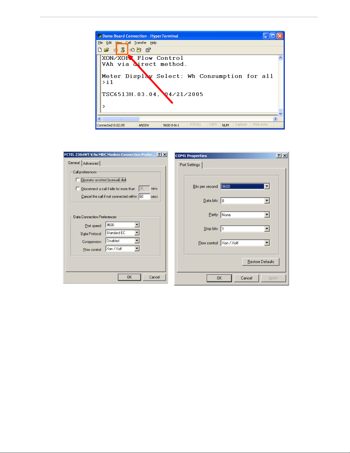
Properties and then clicking on the “Connect Using“ dialog box. If the U S B-to-serial driver is installed (see s ection 1.7.2.1) a port with a number not corresponding to an actual serial port, e.g., COM5, will appear in the dialog box. This port should be selected for the USB connection.
HyperTerminal can be found by selecting Programs Accessories Communicati ons from the Windows
menu. The connection parameters ar e configured by selecting File Properties and then by pressing the Configure button. Port speed and flow control are configured under the General tab (Figure 1-3, left), bit settings are
configured by pressing the Configur e button (Figure 1-3, right), as s hown below. A setup file (file name “Demo
Board Connection.ht”) for Hyper Terminal that can be loaded with Fil e Open is also provided with the to ols
and utilities.
Port parameters can only be adjusted when the connection is not active. The disconnect
button, as shown in Figure 1-2 must be clicked in order to disconnect the port.
start
9 Rev 4.0
Page 10
71M6541 Demo Board REV 3.0 User’s Manual
Figure 1-2: HyperTerminal Sample Window with Disconnect Button (Arr ow)
Figure 1-3: Port Speed and Handshake Setup (left) and Port Bit setup (right)
Once, the connection to the demo board is established, press <CR> and the command prompt,
pear. Type
>? to see the Demo Code help menu. Type >i to ver ify the demo code revision.
>, should ap-
1.8 USING THE DEMO BOARD
The 71M6541 Demo Board is a ready-to-use meter prepared for use with external sh unt resistors.
Demo Code versions for single-phase two-wire operation (EQU 0, with secondary tamper sensor) and for sin-
gle-phase three-wire operation ( A N S I configuration, EQU 1) are provided by Maxim Integrated. Demo Boards in
ANSI configuration are preloaded with Demo Code for EQU 1, Demo Boards in IEC configuration are preloade d
with Demo Code for EQU 0.
Using the Demo Board involves communicating with the Demo Code via the com mand line interface (CLI). The
CLI allows all sorts of manipulations to the metering parameters, ac c ess to the EEPROM, selection of the displayed parameters, changing calibration factors and many more operations.
Before evaluating the 71M6541 on the Demo B oard, users should get familiar with the commands and responses of the CLI. A complete descriptio n of the CLI is provided in section 1.8.1.
10 Rev 4.0
Page 11
1.8.1 SERIAL COMMAND LANGUAGE
The Demo Code residing in the flash memory of the 71M6541 provides a convenie nt way of examining a nd
modifying key meter parameters via its command line interface (CLI).
The tables in this chapter describe the commands in detail.
Commands for CE Data Access:
] CE D ATA ACCESS Comment
Description: Allows user to read from and write to CE data space.
Usage: ] [Starting CE Data Address] [option]…[option]
Command
combinations:
]A$$$ Read consecutive 16-bit words in Hex, starting at address A
]A=n=n Write consecutive memory values, starting at address A
Example: ]40$$$ Reads CE data words 0x40, 0x41 and 0x42.
]7E=1AD2=9A23 Writes two hexadecimal words starting @ 0x7E
]10=+16384 Writes one decimal word starting @ 0x10
All CE data words are in 4-byte (32-bit) format. Typing ]A? will access the 32-bit word located at the b yte address 0x0000 + 4 * A = 0x1028.
]A??? Read consecutive 16-bit words in Decimal, starting at ad-
71M6541 Demo Board REV 3.0 User’s Manual
dress A
Commands for MPU/XDATA Access:
) MPU DATA ACCESS Comment
Description: Allows user to read from and write to MPU data space.
Usage: ) [Starting MPU Data Address] [option]…[option]
Command
combinations:
)A$$$ Read three consecutive 32-bit words in Hex, starting at ad-
)A=n=m Write the values n and m to two consecutive addresses start-
?) Display useful RAM addresses.
Example: )08$$$$ Reads data words 0x08, 0x0C, 0x10, 0x14
)04=FFFFAD2=9A23 Writes two hexadecimal words starting @ 0x04
)04=+1000 Writes decimal 1,000 to address 0x04
)04=-1000 Writes decimal -1,000 to address 0x04
MPU or XDATA space is the address range for the MPU XRAM (0x0000 to 0xFFF). All MPU data words are in 4-byte (32-bit)
format. Typing ]A? will access the 32-bit word located at the byte address 4 * A = 0x28. The energy accumulation registers of
the Demo Code can be accessed by typing two Dollar signs (“$$”), typing question marks will display negative decimal values
if the most significant bit is set.
)A??? Read three consecutive 32-bit words in Decimal, starting at
address A
dress A
ing at address A
11 Rev 4.0
Page 12
71M6541 Demo Board REV 3.0 User’s Manual
Command
Command
combinations:
Command
combinations:
Commands for I/O RAM (Configuration RAM) and SFR Control:
R I/O RAM AND SF R CONTROL Comment
Description: Allows the user to read from and write to DIO RAM and special function registers (SFRs).
Usage: R [option] [register] … [option]
combinations:
Rx… Select internal SFR at address x
Ra???... Read consecutive SFR registers in Decimal, starting at ad-
Ra$$$... Read consecutive registers in Hex, starting at address a
Ra=n=m… Set values of consecutive registers to n and m starting at
Example: RI2$$$ Read DIO RAM registers 2, 3, and 4 in Hex.
The SFRs (special function registers) are located in internal RAM of the 80515 core, starting at address 0x80.
Commands for EEPROM Control:
EE EEPROM CONTROL Comment
Description: Allows user to enable read from and write to EEPROM.
Usage: EE [option] [arguments]
RIx… Select I/O RAM location x (0x2000 offset is automatically
added)
dress a
address a
EECn EEPROM Access (1 Enable, 0 Disable)
EERa.b Read EEPROM at address 'a' for 'b' bytes.
EESabc..xyz Write characters to buffer (sets Write length)
EETa Transmit buffer to EEPROM at address 'a'.
EEWa.b...z Write values to buffer
CLS Saves calibration to EEPROM
Example: EEShello
EET$0210
Due to buffer size restrictions, the maximum number of bytes handled by the EEPROM command is 0x40.
Writes 'hello' to buffer, then transmits buffer to EEPROM starting at address 0x210.
Commands for Flash Memory Control:
F FLASH CONTROL Comment
Description: Allows user to enable read from and write to Flash memory.
Usage: F [option] [arguments]
FRa.b Read Flash at address 'a' for 'b' bytes.
FSabc..xyz Write characters to buffer (sets Write length)
FTa Transmit buffer to Flash memory at address 'a'.
FWa.b...z Write string of bytes to buffer
Example: FShello
FT$FE10
Writes 'hello' to buffer, then transmits buffer to EEPROM starting at address 0xFE10.
12 Rev 4.0
Page 13

71M6541 Demo Board REV 3.0 User’s Manual
Auxiliary Commands:
Typing a comma (“,”) repeats the comman d issued from the previous command line. This is very helpful when
examining the value at a certain addres s over time, such as the CE DRAM addr ess for the temperature (0x40).
The slash (“/”) is useful to separate comments from commands when sending macro text files via the s erial interface. All characters in a line af ter the slash are ignored.
Commands controlling the CE, TMUX and the RTM:
C COMPUTE ENGINE,
Comment
MEMORY, AND CALIBRATION CONTROL
Description: Allows the user to enable and configure the compute engine, store and recall configurations, and
Usage: C [option] [argument]
Command
combinations:
CTn.m Selects the signal for the TMUX output pins (n = 1 for
CREn RTM output control (1 Enable, 0 Disable)
CRSa.b.c.d Selects CE addresses for RTM output
CLS Stores calibration and other settings to EEPROM.
CLR Restores calibration and other settings from EEPROM.
CLD Restores calibration and other settings to defaults.
CLB Start auto-calibration based on voltage (MPU address 0x17,
CLC Apply machine-readable calibration control (Intel Hex-
CPA Start the accumulating periodic pulse counters.
CPC Clear the pulse counters
CPDn Activate pulse counters for n seconds
Example: CE0 Disables CE, (“SYS will stop blinking on the LCD).
CT1.3 Selects the VBIAS signal for the TMUX output pin
initiate calibration.
CEn Compute Engine Enable (1 Enable,
0 Disable)
TMUXOUT, n = 2 for TMUX2OUT). m is interpreted as a dec-
imal number.
current (MPU 0x18), and duration (MPU 0x16) in seconds.
Records).
Commands for Identification and Information:
I INFORMATION MESSAGES Comment
Description: Allows the user to read information messages.
Usage: I Sends complete demo code version information on serial inter-
M0 Displays meter ID on LCD.
The I command is mainly used to identify the revisions of Demo Code and the contained CE code.
face.
13 Rev 4.0
Page 14
71M6541 Demo Board REV 3.0 User’s Manual
Command
combinations:
Commands for Battery Mode Control and Battery Test:
B I NFO RMATION MESSAGES Comment
Description: Allows the user to control battery modes and to test the battery.
Usage: BL Enters LCD mode when in brownout mode (B> prompt).
BS Enters sleep mode when in brownout mode (B> prompt).
BT Starts a battery test – when in mission mode (> prompt).
BWSn Set wake timer to n seconds for automatic return to brownout
mode.
BWMn Set wake timer to n minutes for automatic return to brownout
mode.
Commands for Controlling the RTC:
RT REAL-TIME CLOCK CON-
Comment
TROL
Description: Allows the user to read and set the real time clock.
Usage: RT [option] [value] … [value]
Command
combinations:
RTR Read Real Time Clock.
RTTh.m.s Time of day: (hr, min, sec).
RTAs.t Real Time Adjust: (start, trim). Allows trimming of the RTC.
> Access look-up table for RTC compensation.
Example: RTD05.03.17.5 Programs the RTC to Thursday, 3/17/2005
RTA1.+1234 Speeds up the RTC by 1234 PPB.
>0???? Read the first four bytes in the look-up table.
RTDy.m.d.w: Day of week (year, month, day, weekday [1 = Sunday]). If the weekday is
omitted it is set automatically.
If s > 0, the speed of the clock will be adjusted by ‘t’ parts per
billion (PPB). If the CE is on, the value entered with 't' will be
changing with temperature, based on Y_CAL, Y_CALC and
Y_CALC2.
The “Military Time Format” is used for the RTC, i.e., 15:00 is 3:00 PM.
Commands for Accessing the Trim Control Registers:
T TRIM CONTROL Comment
Description: Allows user to read trim and fuse values.
Usage: T [option]
T4 Read fuse 4 (TRIMM).
T5 Read fuse 5 (TRIMBGA)
T6 Read fuse 6 (TRIMBGB).
Example: T4 Reads the TRIMM fuse.
These commands are only accessible for the 71M6541H (0.1%) parts. When used on a 71M6541 (0.5%) part,
the results will be displayed as zero.
14 Rev 4.0
Page 15
71M6541 Demo Board REV 3.0 User’s Manual
Reset Commands:
W RESET Comment
Description: Watchdog control
Usage: W Halts the Demo Code program, thus suppressing the trigger-
Commands for the 71M6X0X Remote Sensor Interface:
6 71M6X0X Interface Comment
Description: Commands for control of the Re-
mote Sensor Interface IC.
Usage: 6En Remote sensor Enable (1 Enable, 0 Disable)
6Ra.b Read Remote Sensor IC number a with command b.
6Ca.b Write command b to Remote Sensor IC number a.
6Ta.b Send command b to Remote Sensor IC number a in a loop
6T2 Send temp command to 6000 number 2 in a loop forever.
6R1.20 Reads the temperature from Remote Sensor IC number 1.
ing of the hardware watchdog timer. This will cause a reset, if
the watchdog timer is enabled.
forever.
15 Rev 4.0
Page 16

71M6541 Demo Board REV 3.0 User’s Manual
1.04 Whr
04
2.21 VARhr
05
0.95 VARhr
06
07
0.7 hr
08
01:43:59
09
01.01.01
10
1
120
13
14
24.10 A
15
241.27 V
16
3.34 V
17
1
50400 W
19
88.88.88
Commands for Controlling the Metering Values Shown on the LCD Display:
Step
0
1
2
3
4
5
6
7
8
9
Text or Nu-
merical Dis-
play
10000
00
24.5 °C
01
59.9
02
3.27 Whr
03
4.11 VAhr
CLI
command
M0
M1
M2
M3
M4
M5
M6
M7
M8
M9
Displayed Parameter(s)
Meter ID
Temperature difference from calibr ation temperature.
Frequency at the VA_IN input [Hz]
Accumulated imported real energy [Wh]. The default display setting
after power-up or reset.
Accumulated exported real energy [Wh].
Accumulated reactive energy [V ARh].
Accumulated exported reactive energy [VARh].
Accumulated apparent energy [V A h].
Elapsed time since last reset or power up.
Time of day (hh.mm.ss)
10
11
12
13
14
15
16
17
18
19
20
0.62
11
0
48
241.34 W
18
88.88.88
88.88.88
M10
M11.P
M12
M13
M14
M15.P
M16
M17
M18
M19
M20
Date (yy.mm.dd)
Power factor (P = phase)
Not used in the 71M6541
Zero crossings of the mains voltage
Duration of sag or neutral current [s]
RMS current (P = phase)
RMS voltage
Battery voltage
Momentary power in W (P = phase)
Demand
LCD Test
Displays for total consumption wrap around at 999.999Wh (or VARh, VAh) due to the limited number of available display digits. Internal registers (counters) of the Demo Code are 64 bits wide and do not wrap around.
16 Rev 4.0
Page 17

71M6541 Demo Board REV 3.0 User’s Manual
1.8.2 USING THE DEMO BOARD FOR ENERGY MEASUREMENTS
The 71M6541 Demo Board was designed for use with shunt resistors connected directly t o the IAP/IAN pins of
the 71M6541 and via the Remote Sensor I nterface and it is shipped in this configuration.
The Demo Board may immediately be used with a 50 µΩ shunt resistor (ANSI) or a 120 µΩ shunt resistor (IEC).
It is programmed for a kh factor of 1.0 (see Section 1.8.4 for adjusting the Demo Board for shunts with different
resistance).
Once, voltage is applied and load current is flowing, the red LED D5 will f l ash each time an energy sum of 1.0
Wh is collected. The LCD display wil l show the accumulated energy in Wh whe n s et to display mode 3 (com-
>M3 via the serial interface).
mand
Similarly, the red LED D6 will flas h each time an energy sum of 1.0 VARh is collected. The LCD display will
show the accumulated energy in VARh when set to display mode 5 (command
>M5 via the serial interface).
1.8.3 ADJUSTING THE KH FACTOR FOR THE DEMO BOARD
The 71M6541F Demo Board is shipped with a pre-programmed scaling factor Kh of 1.0, i.e., 1.0 Wh per pulse.
In order to be used with a calibrated loa d or a meter calibration system, the boar d should be connected to the
AC power source using the spade terminals on the bottom of the board. The shunt resistor should be connected
to the dual-pin header labeled J3 on the bottom of the board.
The Kh value can be derived by reading the values for IMAX and VMAX (i.e., the RMS current and voltage values that correspond to the 250mV maximum input signal to the IC), and insert i ng them in the following equation
for Kh:
Kh = 109.1587*
See the explanation in section 1.10.4 for an exact definition of the constants and variables involv ed i n the equation above.
VMAX*IMAX / (SUM_SAMPS*WRATE*X),
1.8.4 ADJUSTING THE DEMO BOARDS TO DIFFERENT SHUNT RESISTORS
The Demo Board is prepared for use with 120 µΩ or 50 µΩ (ANSI option) shunt resistors in both current channels. For the Demo Board, a certain current flowing through the 120 µΩ shunt resistor will result in the maximum
voltage drop at the ADC of the 71M6541. This current is defined as IMAX.
IMAX will change when different values are used for the shunt r es i s tor(s) which will require that
be updated as shown in section 1.10.4.
WRATE has to
1.8.5 USING THE PRE-AMPLIFIER
In its default setting, the 71M6541 is applies a gain of 1 to the current input for phase A (IAP/IAN pins). This
gain is controlled with the PRE_E bit in I/O RAM (r efer to the IC data sheet). The command line interface (RI
command) can be used to set or reset this bit. It is recommended to maintain the gain of setting of 1
(RI2704=0x90).
1.8.6 USING CURRENT TRANSFORMERS (CTs)
Phase B of the 71M6541 Demo Board can be equipped with a CT that may be connected at header J8. A burden resistor of 1.7 Ω, or any other value m ay be installed at the R33 and R34 locations. With a 2000:1 ratio CT,
the maximum current fort phase B will be 208 A.
Note: The CT configuration will require a different version of the Demo Code.
Current measurements can be displa ye d for phase B by the demo code, and the corr esponding currents can be
extracted by the MPU from the CE register s for tamper detection when using the Demo Code for EQU 0.
1.8.7 IMPLEMENTING A SINGLE-PHASE 3-WIRE METE R (EQU 1)
This application will require two identical current sensors for eac h phase. The simplest approach is to use identical shunt resistors for each channel .
1.8.8 ADJUSTING THE DEMO BOARDS TO DIFFERENT VOLTAGE-DIVIDERS
The 71M6541 Demo Board comes equipped with its own network of resist or dividers for voltage measurement
mounted on the PCB. The resistor values (for the D6541 REV 3.0 Demo Board) are 2.5 477MΩ (R15-R21, R26R31 combined) and 750Ω (R32), resulti ng in a ratio of 1:3,393.933. Thi s means that
176.78mV*3,393.933 = 600V. A large value for VMAX has been selected in order t o have headroom for
17 Rev 4.0
VMAX equals
Page 18

71M6541 Demo Board REV 3.0 User’s Manual
overvoltages. This choice need not be of concern, since the ADC in the 71M6541 has enough resolution, even
when operating at 120Vrms or 240Vrms.
If a different set of voltage-dividers or an external voltage transformer (potential transformer) is to be used,
scaling techniques should be used.
In the following example we assume that the line voltage is not applied t o the resistor divider for VA formed b y
R15-R21, R26-R31, and R32, but to a volt age transformer with a ratio N of 20:1, followed by a simple resistor
divider. We also assume that we want t o m aintain the value for
voltage excursions.
VMAX at 600V to provide headroom for large
When applying
is scaled by the resistor divider rat i o RR. When the input voltage to the voltage channel of the 71M6541 is the
V
s
desired 177mV, V
VMAX at the primary side of the transformer, the secondary voltage V
= VMAX / N
V
s
is then given by:
s
V
= RR * 177mV
s
Resolving for RR, we get:
= (VMAX / N) / 177mV = (600V / 30) / 177mV = 170.45
R
R
This divider ratio can be implemented, for example, with a combination of one 16.95 kΩ and one 100 Ω resistor.
If potential transformers (PT s ) are used instead of resistor dividers, phase shifts will be introduced that will re-
quire negative phase angle compens ation. Maxim Integrated Demo C ode accepts negative calibration f ac tors
for phase.
1.9 CALIBRATION PARAMETERS
1.9.1 GENERAL CALIBRATION PROCEDURE
Any calibration method can be used with the 71M6541F chips. This Demo Board User’s Manual present s calibration methods with three or fiv e measurements as recommended methods, because they work with most
manual calibration systems based on counting "pulses" (emitted by LEDs on the meter).
Naturally, a meter in mass production will be equipped with special calibration code offering capabilities beyond
those of the 71M6541 Demo Code. It is basically possible to calibrate using voltage and current readings, with
or without pulses involved. For this purpose, the MPU Demo Code can be modif ied to display averaged voltage
and current values (as opposed to momentary values). Also, automate d c al ibration equipment can communicate with the Demo Boards via the serial interface and extract voltage and current readings. This is possible
even with the unmodified Demo Code.
Complete calibration procedur es are given in section 2.3 of this manual.
Regardless of the calibration proc edure used, parameters (calibration factors) will result that will have to be ap-
plied to the 71M6541F chip in order to make the chip apply the modified gains and phase shifts necessary for
accurate operation. Table 1-4 s hows the names of the calibration factors, their function, and their location in the
CE RAM.
Again, the command line interface can be used to store the calibration factors in their respective CE RAM addresses. For example, the command
>]10=+16302
is:
s
stores the decimal value 16302 in the CE RAM location controlling the gain of the current channel (
CAL_IA).
The command
>]11=4005
stores the hexadecimal value 0x4005 (decimal 16389) in the CE RAM loc ation controlling the gain of the voltage channel (
CAL_VA).
The internal power supply generat es a ripple on the supply and ground nets that is 90° phase shifted with respect to the AC supply voltage. This affects the accuracy of the VARh measurements. If optimization of the
VARh accuracy is required, this can be done by writing a value into the QUANT_VAR regist er of the CE (see
section 2.3.7).
18 Rev 4.0
Page 19
Table 1-4: CE RAM Locations for Calibration Constants
CE0 /disable CE
CE1 /enable CE
CE Ad-
Coefficient
CAL_VA
CAL_IA
CAL_IB
PHADJ_A
LCOMP2_B
dress
(hex)
0x11
0x10
0x13
0x12
0x15
Description
Adjusts the gain of the voltage chan nels. +16384 is the typical value. The
gain is directly proportional to the CAL parameter. Allowed range is 0 to
32767. If the gain is 1% slow, CAL should be increased by 1%.
Adjusts the gain of the current chann el s . +16384 is the typical value. The
gain is directly proportional to the CAL parameter. Allowed range is 0 to
32767. If the gain is 1% slow, CAL should be increased by 1%.
This constant controls the phase compensation. No compensation occurs
in a phase when PHADJ_A = 0 or when LCOMP2_n = 16384. As
LCOMP2_n is increased, more compensation is introduced.
CE codes for CT configuration do not use delay adjustment. These codes
use phase adjustment (
1.9.2 CALIBRATION MACRO FILE
The macro file in Figure 1-4 contains a sequence of the serial interface commands. It is a simple text file and
can be created with Notepad or an equivalent ASCII editor program. The file is executed with HyperTerminal’s
Transfer->Send Text File command.
71M6541 Demo Board REV 3.0 User’s Manual
PHADJ_n).
]10=+16022 /CAL_IA (gain=CAL_IA/16384)
]11=+16381 /CAL_VA (gain=CAL_VA/16384)
]12=+115 /PHADJ_A (default 0)
Figure 1-4: Typical Calibration Macro File
It is possible to send the calibration mac ro file to the 71M6541F for “temporary” calibration. This will temporaril y
change the CE data values. Upon power up, these values are refreshed back to the default values stored in
flash memory. Thus, until the flash memory is updated, the macro file must be loaded each time the part is
powered up. The macro file is run by sending it with the transfer
Use the Transfer Send Text File command!
1.9.3 UPDATING THE DEMO CODE (HEX FILE)
The d_merge program updates t he hex file (usually named 6541_1p2b_19jan09.hex or similar) with th e values
contained in the macro file. This pro gram is executed from a DOS command line window. Executing the
d_merge program with no arguments will display the syntax description. To merge macro.txt and
old_6541_demo.hex into new_6541_demo.hex, use the command:
d_merge old_6541_demo.hex macro.txt new_6541_demo.hex
The new hex file can be written to the 71M6541F/71M6541H through the ICE port using the ADM-51 in-circuit
emulator or the TFP-2 flash programmer.
send text file procedure of HyperTerminal.
19 Rev 4.0
Page 20

71M6541 Demo Board REV 3.0 User’s Manual
1.9.4 UPDATING CALIBRATION DATA IN FLASH O R EEPROM
It is possible to make data permanent that had been entered temporarily into the CE RAM. The transfer t o
EEPROM memory is done using the following serial interface command:
>]CLS
Thus, after transferring calibration data with manual serial int er face commands or with a macro file, all that has
to be done is invoking the U command.
Similarly, calibration data can be restored to default values using the CLD command.
After reset, calibration data is cop ied from the EEPROM, if present. Otherwise, calibration
data is copied from the flash memory. Writing 0xFF into the first few bytes of the EEPROM
deactivates any calibration data p r eviously stored to the EEPROM.
1.9.5 LOADING THE CODE FOR THE 71M6541 INTO THE DEM O BOARD
Hardware Interface for Programming: The 71M6541F IC provides an interface for loading code into the inter-
nal flash memory. This interface consi s ts of the following signals:
E_RXTX (data), E_TCLK (clock), E_RST (reset), ICE_E (ICE enable)
These signals, along with V3P3D an d GND are available on the emulator h eaders J14.
Programming of the flash memory requires a specific in-circuit emulator, the ADM-51 by Signum Systems
(www.signum.com) or the Flash Programmer (T FP2) available through Digi-Key (www.digikey.com) or Mouser
Electronics (www.mouser.com).
Chips may also be programmed before t hey are soldered to the board. Gang programmers suitable for highvolume production are availab le from BPM Microsystems (www.bpmmicro.com).
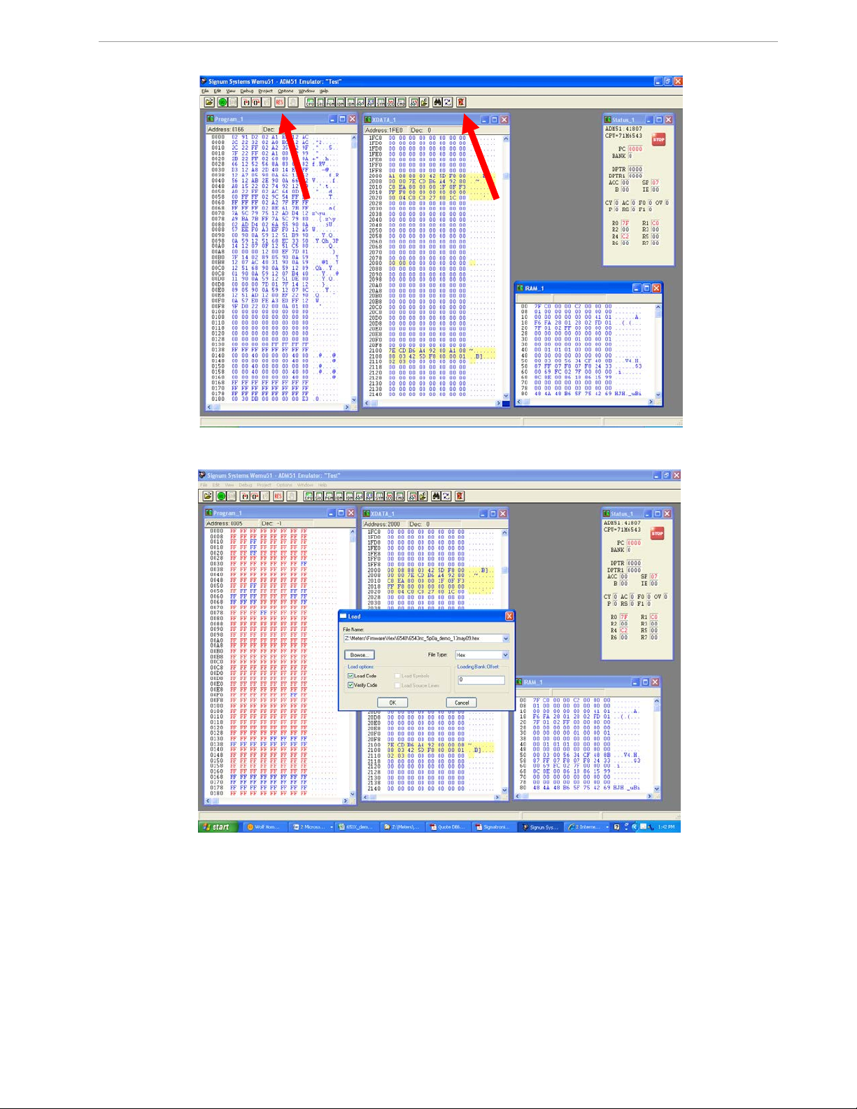
In-Circuit Emulator: If firmware exists in the 71M6541F flash memory; it has t o be erased before loading a new
file into memory. Figure 1-5 and Figure 1-6 show the emulator software active. In order to erase the flash
memory, the RESET button of the emulator software has to be clicked followed by the ERASE button.
To successfully erase the flash memory, the following steps have to be taken :
1) Disable the CE by writing 0x00 to addres s 0x2000
2) Write 0x20 to address 0x2702 (
3) Reset the demo board (RESET button or power cycle)
4) Activate the ERASE button in the WEMU51 user interface
5) Now, new code can be loaded into the flash memory
Once the flash memory is erased, the new file can be loaded using the comm ands File followed by Load. The
dialog box shown in Figure 1-6 will then appear making it possible to select the file to be loaded by clicking the
Browse button. Once the file is sel ec ted, pressing the OK button will loa d the file into the flash memory of t he
71M6541F IC.
At this point, the emulator probe (cab le) can be removed. Once the 71M6541F IC is reset using the reset button
on the Demo Board, the new code starts executing.
FLSH_UNLOCK[ ] register in I/O RAM)
20 Rev 4.0
Page 21
71M6541 Demo Board REV 3.0 User’s Manual
Figure 1-5: Emulator Window Showing Reset and Erase Buttons (see Arrows)
Figure 1-6: Emulator Window Showing Erased Flash Memory and File Load Menu
Flash Programmer Module (TFP-2): The operational firmware of the T FP 2 will have to be upgraded to revision
1.53. Follow the instructions given in the User Manual for the TFP-2.
21 Rev 4.0
Page 22

71M6541 Demo Board REV 3.0 User’s Manual
Signal
Direction
Function
ICE_E
Input to the 71M6541
ICE interface is enabled when ICE _E is
pulled high
E_TCLK
Output from 71M6541
Data clock
E_RXTX
Bi-directional
Data input/output
E_RST
Bi-directional
Flash Downloader Reset (active low)
1.9.6 THE PROGRAMMING INTERFACE OF THE 71M6541
Flash Downloader/ICE Interface Signals
The signals listed in Table 1-5 are neces sary for communication between the Flash Downloader or ICE and the
71M6541.
Table 1-5: Flash Programming Interface Signals
The E_RST signal should only be driven by the Flash Downloader when enabli ng these interface
signals. The Flash Downloader mus t release E_RST at all other times.
22 Rev 4.0
Page 23

1.10 DEMO CODE
1.10.1 DEMO CODE DESCRIPTION
The Demo Board is shipped preloade d with Demo Code in the 71M6541F chip. The code r ev i s i on can easily be
verified by entering the command >i v i a the serial interface (see sectio n 1.8.1). Check with your local Maxim Integrated representative or FAE for the latest revision.
The Demo Code is provided in two diff er ent versions:
• Single-phase two-wire operation (EQU 0, with secondary tamper sensor). Energy measurement and
Wh/VARh pulses are based solely on VA (phase A voltage) and IA (phase A current). Energy and current values for IB (secondary phase) are available as CE outputs to the MPU f or processing of tampering events.
• Single-phase three-wire operation ( ANSI configuration, EQU 1). E ner gy measurements and Wh/VARh
pulses are based on VA (IA – IB) / 2.
71M6541 Demo Board REV 3.0 User’s Manual
Both Demo Code versions use the same CE code, but with different settings of the
The Demo Code offers the following features:
• It provides basic metering functions such as pulse generation, display of accumulated energy, fre-
quency, date/time, and enables the user to evaluate the parameters of the metering IC such as accuracy, harmonic performance, etc .
• It maintains and provides access to basi c household functions such as the real-time clock (RTC).
• It provides access to control and dis pl ay functions via the serial interface, enabling the user to vie w
and modify a variety of meter parameters such as Kh, calibration coefficients, temperature compensation etc.
• It provides libraries for access of low-level IC functions to serve as building blocks for code de-
velopment.
A detailed description of the Demo C ode can be found in the Software User’s G uide (SUG). In addition, the
comments contained in the librar y prov ided with the Demo Kit can serve as usef ul documentation.
The Software User’s Guide contains the following information:
• Design guide
• Design reference for routines
• Tool Installation Guide
• List of library functions
• 80515 MPU Reference (hardware, instruction set, memory, register s)
1.10.2 IMPORTANT MPU ADDRESSES
In the demo code, certain MPU XRAM para m eters have been given addresses in order to permit easy external
access. These variables can be read via the command line interface (if available), with the )n$ com mand and
written with the )n=xx command where n is the word address. Note that accumulat ion variables are 64 bits long
and are accessed with )n$$ (read) and )n=hh=ll (write) in the case of accumulat ion variables.
The first part of the table, the addr esses )00..)1F, contains adjustments, i.e., numbers that may need adjustment in a demonstration meter, and so are par t of the calibration for demo code. In a r eference meter, these
may be in an unchanging table in code space.
The second part, )20..)2F, pertains to calibration, i.e., variables that are likely to need indivi dual adjustments for
quality production meters.
The third part, )30…, pertains to meas ur ements, i.e., variables and regi s ters that may need to be read in a
demonstration meter.
EQU register.
23 Rev 4.0
Page 24

71M6541 Demo Board REV 3.0 User’s Manual
Table 1-6: MPU XRAM Locations
Name Purpose LSB Default )? Signed? Bits
Metering element
enters creep mode
if current is below
this value.
i_min
cfg
v_min
i_max
v_max
i_limit
If 0, creep logic is
disabled. In creep
Same units as CE’s i0sqsum. 0.08A )0 signed 32
mode, on each metering element, Wh,
VARh, i0sqsum,
and other items are
zeroed.
bit0: 1=Display KWh.
bit1: 1=clear accumulators, er-
rors, etc. (e.g., “)1=2”)
bit2: 1=Reset demand. (e.g.,
“)1=4”)
bit3: 1=CE Raw mode. MPU
does not change CE values with
creep or small current calcula-
tions.
bit5: 1= Send a message once
Configure meter
operation on the fly.
per second for IEC 62056-217
Mode D on UART 1, at 2400
BAUD, even parity. The meter’s
serial number and current Wh
display are sent as data. UART
1 is routed to an IR LED if pos-
sible. Mode D data fields are
prefaced with OBIS codes in
legacy format.
7,1
bit6: 1=Auto calibration mode
bit7: 1=Enable Tamper Detect
2,1
error if below. Also
creep.*
Below this, low voltage seconds are
counted. Voltage,
Same units as CE’s v0sqsum. 40V )2 signed 32
Wh, VARh, Frequency, and other
voltage-dependent
items are zeroed.
Scaling Maximum
Amps for standard
0.1A
sensor.
Scaling Maximum
Volts for PCB
0.1V
Error if exceeded. Same units as CE’s i0sqsum.
0
Do nothing special.
1
110.5 for 200
μΩ shunt with
8x preamp.
884.0 A for 200
μΩ shunt,
442.0A for 400
μΩ shunt.
600 V, for the
6541 REV 3.0
Demo Board.
50.9A =
30A*sqrt(2)
*120%
)1 N/A 8
)3 signed 16
)4 signed 16
)5 signed 32
24 Rev 4.0
Page 25

v_limit
wrate_mpu
interval
mains_hz
temp_cal1
mtr_cal1
[0..3]
mtr_cal2
[0..3]
9
9
y_datum
y_cal1 5
y_cal2 5
s_cal 1
v_cal 1
i_cal 1
71M6541 Demo Board REV 3.0 User’s Manual
Error if exceeded.* Same units as CE’s v0sqsum.
CE’s w0sum units per pulse,
Convert from CE
counts to pulses.
The number of
minutes of a demand interval.
Expected number of
cycles per second
of mains. 0 disables
the software RTC
run from mains.
Machine-readable
units per 0.1C
Linear temperature
calibration for meter
elements A..D.
Squared temperature calibration for
meter elements
A..D.
Center temperature
of the crystal.
RTC adjust, linear
by temp.
RTC adjust,
squared by temp.
Accumulation intervals of
Autocalibration
Volts of
Autocalibration
Amps of
Autocalibration
rounded up to next largest CE
count so Wh accumulation and
display is always rounded down.
Count of minutes.
(60/interval)*interval = 60.
Hz 0 )9 unsigned 8
Refer to the IC data sheet.
Temperature is calculated as
temp = (measured_temp –
temp_datum)/temp_cal1 +
temp_cal0
ppm*(T - mtr_datum), in 0.1˚C 150 )B..E signed 16
ppm2*(T - mtr_datum)2, in 0.1˚C -392
0.1C 25C )13 signed 16
10ppb*(T - y_datum), in 0.1˚C 0 )14 signed 16
1ppb*(T - y_datum)2, in 0.1˚C 38 )15 signed 16
Count of accumulation intervals
of calibration.
0.1V rms of AC signal applied to
all elements during calibration.
0.1A rms of AC signal applied to
all elements during calibration.
Power factor of calibration sig nal
must be 1.
407.3V =
240V*sqrt(2)
)6 signed 32
*120%
3.2 Wh for 3phase
1.0 Wh for 1-
)7 signed 32
phase
2 minutes. )8 unsigned 8
Refer to the IC
data sheet.
)A signed 32
)F..1
2
signed 16
accumulation
intervals cover
both chop polar-
)16 signed 16
ities.
2400
240 V is a
standard full-
)17 signed 16
scale setup for
meter test.
300
30 A is a stand-
ard full-scale
)18 signed 16
setup for meter
test.
25 Rev 4.0
Page 26

lcd_idx
lcd_bit
mfr_id 6
Selects LCD’s current display.
Defines sequence
of LCD displays.
Manufacturer’s ID
text string of the
meter
71M6541 Demo Board REV 3.0 User’s Manual
0: Meter identification. (“#”)
1: Display variation from calibra-
tion temperature, 0.1C
2: Display mains Hz, 0.1 Hz
3: mWh, total
4: mWh total exported.
5: mVARh, total.
6: mVARh, total exported.
7:mVAh, total
8: Operating hours.
9: Time of day
10: Calendar date
11: Power factor, total
12: Angle between phase 0 & 1
13: Main edge count, last accu-
mulation.
14: KW, instantaneous total
15: V, instantaneous max of all
phases.
16: A, total
17: V, Battery (“VB”)
18: Seconds, bad power (“BPS”)
19: Seconds, tamper (- = tamper
in progress) (“TS”)
20: LCD Test
Scrolling not standard for these:
111: PF, phase 0
112: Angle, phase 0 & 1
114: KW, phase 0
115: V, phase 0
116: A, phase 0
211: PF, phase 1
212: Angle, phase 0 & 2
214: KW, phase 1
215: V, phase 1
216: A, phase 1
311: PF, phase 2
312: Angle, phase 2.0
314: KW, phase 2
315: V, phase 2
316: A, phase 2
416: A, neutral (measured)
The value is a bit mask that describes a scrolling display sequence. Each set bit permits a
display with an lcd_idx value
from 0..31. Each is displayed for
7 seconds. Ordered by increasing bit number. If value is zero,
display does not change.
3 ASCII bytes, in MSB of 32-bit
number. Least significant byte
should be zero. For AMR
demonstrations, sent as the
manufacturer’s ID of the meter.
3 )19 signed 16
0 )1A unsigned 32
“TSC”,
0x54534300
)1B unsigned 32
26 Rev 4.0
Page 27

71M6541 Demo Board REV 3.0 User’s Manual
Like i_max, except
for the 2nd current
sensor.
i_max2 4
in_limit 3
in_wait 3
Reserved )1F
meter_id 8
temp_datum 8
mtr_datum[0.
.3]8
rtca_adj 8
y_cal0 5,8
v_bat_min 8
cal_cnt
ver_hash
data_ok_cal
Reserved
Currents, Wh etc.
using currents from
the second sensor
are rescaled into the
same units as the
first current sensor.
Maximum valid neutral current.
The time that neutral current can exceed n_max before
the neutral error is
asserted.
Identification number of meter.
Count of temperature sensor at calibration.
Center temperature
of a meter element’s
temperature curve.
Default value for
RTCA_ADJ, the
crystal’s capacitor
adjustment.
RTC offset rate adjust
Minimum valid battery voltage.
Count of calibrations. In demo code,
it also checks adjustments.
Checked to prevent
old calibration data
from being used by
new code. Value
that changes with
the banner text, and
therefore with the
version, date and
time.
Checks calibrations.
In demo code, it
also checks adjustments.
0.1 Amps 208 A (2080) )1C signed 16
Same units as CE’s i3sqsum. 0.1A )1D signed 32
Count of accumulation intervals. 10 secs. )1E signed 16
32 bit unsigned number. For
AMR demonstrations, this is
sent in decimal as the identification number of the meter.
Refer to the IC data sheet.
Temperature is calculated as
temp = (measured_temp –
temp_datum)/temp_cal1 +
temp_cal0
0.1C 22C
Refer to the IC data sheet. Set
from hardware value when
hardware is changed.
100ppb 0 )27 signed 16
Units of hardware’s battery
measurement register.
Counts number of times calibration is saved, to a maximum of
255.
Uses data_ok() to calculate a
value from the string.
Checked by data_ok() of calibr ation value.
100000000 )20 signed 32
n/a )21 signed 32
)22..
25
Hardware default (refer to
the IC data
sheet).
2V on a real
PCB; should be
adjusted for
battery and
chip.
0 )29 unsigned 8
n/a )2A unsigned 8
n/a )2B unsigned 16
)26 unsigned 8
)28 signed 32
)2C.
)2F
signed 16
27 Rev 4.0
Page 28

71M6541 Demo Board REV 3.0 User’s Manual
data_ok_reg
state_bit_ar
y
Status of meter.
Nonvolatile.
Bits:
See table below.
0 = no errors )30 unsigned 32
First 32-bit number is a count of
wh_im
Wh energy register.
Nonvolatile.
pulses, =3.2 Wh in 3-phase meters, or 1 in 1-phase. A fractional
pulse is present in the CE data,
n/a )31 64
but not preserved.
Wh exported energy
wh_ex
register. Nonvola-
Like wh_im n/a )32 64
tile.
varh_im
varh_ex
dmd_max
dmd_max_rtc
VARh register.
Nonvolatile.
VARh exported register. Nonvolatile.
Maximum demand,
W
Time of maximum
demand.
Like wh_im n/a )33 64
Like wh_im n/a )34 64
Units of w0sum n/a )35 signed 32
Standard time and date struc-
ture.
year, month,
date, hour, min
)36..
3A
unsigned 7x8
Battery voltage at
v_bat
last measurement.
Volatile; not saved
0.1V n/a )3B signed 8
on power failure.
Count of accumula-
tion intervals since
reset, or last clear.
acc_cnt
Cleared with )1=2 or
count n/a )3C signed 32
meter read. Volatile;
not saved on power
failure.
Counts seconds
that tamper errors
tamper_sec
were asserted.
Cleared with )1=2 or
This is a tamper measurement. n/a )3D signed 32
meter read. Nonvol-
atile.
Counts seconds
sag_sec
that voltage low
error occurred. or
meter read. Nonvol-
This is a power quality meas-
urement.
n/a )3E signed 32
atile.
Counts seconds
that neutral current
in_sec 3
error was asserted.
Cleared with )1=2 or
This is a power quality meas-
urement.
n/a )3F signed 32
meter read. Nonvolatile.
rtc_copy
save_cnt
Clock time and date
when data was last
read from the RTC.
Number of power
register saves.
Standard time and date struc-
ture. year, month, date, hour,
min, sec
n/a
)40..
45
unsigned 8*7
n/a n/a )46 unsigned 16
Checks data. n/a n/a )47 unsigned 16
1
Valid only when autocalibration is int egrated. Meters with metering equations with differential cur rents or voltages do not
normally support autocalibration.
2
Requires features not in some demo PCBs .
28 Rev 4.0
Page 29

71M6541 Demo Board REV 3.0 User’s Manual
No.
MINIA
0
IA is below IThrshld. Current for this phase is in creep.
MINIB
MINIC
2
IC is below IThrshld. Current for this phase is in creep.
MINVA
3
VA is below VThrshld. Voltage for this phase is in creep.
MINVB
4
VB is below VThrshld. Voltage for this phase is in creep.
MINVC
5
VC is below VThrshld. Voltage f or this phase is in creep.
CREEPV
6
All voltages are below VThrshld.
CREEP
7
There is no combination of current and vo ltage on any phase.
SOFTWARE
8
A software defect was detected. error_software() was called. For example: An impossible value
occurred in a selection, or the tim ers ran out.
NEUTRAL
9
Neutral current was above in_limit for more than in_wait seconds.
SPURIOUS
SAG
11
Voltage was below VThrshld for more than in_wait seconds
DEMAND
12
Demand was too big (too many watts) to be credible.
CALIBRATION
13
Set after reset if the read of the calibrat i on data has a bad checksum, or is from an earlier version of software. The default values should be present.
RTC_UNSET
14
Set when the clock’s current reading is A ) Obtained after a cold start, indic ating that there was
time is preserved, but the clock can’t be trusted.
HARDWARE
15
An impossible hardware condition was detected. For example, the software times out waiting
for RTC_RD to become zero.
BATTERY_BAD
16
Just after midnight, the demo code sets this bit if VBat < VBatMin. The read is infrequent to
read occurs every second, for up to 20 sec onds.
REGISTER_BAD
17
Set after reset when the read of the power register data has a bad longitudi nal r edundancy
check or bad software version in all 5 copies. Unlikely to be an accident.
RTC_TAMPER
18
Clock set to a new value more than two hour s from the previous value.
TAMPER
19
Tamper was detected. Normally this i s a power tamper detected in the creep l ogi c . For example, current detected with no voltage.
3
Three-phase ICs only. Some CE codes calculate neutral current rather than measuring it. Consult the CE documenta-
tion.
4
Only in systems with two current sensors.
5
High accuracy use of this feature may require a calibrated clock.
6
IEC 62056 Manufacturers’ IDs are al located by the FLAG Association Limited. Maxim Integrated does not own or profit
from the FLAG association. Maxim Integrated’s default id may not confor m, and is for demonstration purposes only.
7
Nothing in the document should be interpreted as a guarantee of conformance to a third-party software specification.
Conformance testing is the respons ibility of a meter manufacturer.
8
May require calibration for best accuracy.
9
Calibration item in high-precision “H” series meters (71M6541H only).
Table 1-7: Bits in the MPU Status Word
Bit
Name
Explanation
1 I B i s bel ow IThrshld. Current for this phase is in creep.
10 An unexpected interrupt was detected.
no battery power, and therefore the clock has to be invalid. B) More than a year after the previously saved reading, or C) Earlier than the previously saved reading. In this case, the clock’s
reduce battery loading to very low values. When the battery voltage is being displayed, the
Table 1-8 contains LSB values for the CE registers used in the CE code for E QU 0 and EQU 1. All values are
based on the following settings:
• Gain in amplifier for IAP/IAN pins selected to 1.
• 71M6103 or 71M6113 Remote Sensor Int erface is used.
Note that some of the register contents can be zeroed out by the MPU when it appl ies functions contained in its
creep logic.
29 Rev 4.0
Page 30

1.10.3 LSB VALUES IN CE REGISTERS
Register Name
LSB Value
Comment
1.55124*10
*IMAX*VMAX
The real energy for element 1 (IA, VA), measured in Wh per accum ulation interval
1.55124*10
*IMAX*VMAX
The reactive energy for element 1 (IA, V A), measured in VARh per
accumulation interval
W1SUM_X
1.55124*10
*IMAX*VMAX
lation interval
VAR1SUM_X
1.55124*10
*IMAX*VMAX
The reactive energy for element 2 (IB, VA), measured in VARh per
accumulation interval
I0SQSUM_X
2.55872*10
*IMAX*VMAX
The sum of squared current samples in element 1 (IA). This value is
the basis for the I
RMS
calculation performed in the MPU.
2.5587*10
*IMAX*VMAX
The sum of squared current samples in element 2 (IB). This value is
the basis for the I
RMS
calculation performed in the MPU.
V0SQSUM_X
9.40448*10
-13
*IMAX*VMAX
The sum of squared voltage samples in element 1 (VA).
9.40448*10
*IMAX*VMAX
The sum of squared voltage samples in element 1 (VA). This value is
not used for EQU 0 or EQU 1.
Table 1-8: CE Registers and Associated LSB Values
71M6541 Demo Board REV 3.0 User’s Manual
W0SUM_X
VAR0SUM_X
I1SQSUM_X
V1SQSUM_X
-12
-12
-12
-12
-12
-12
-13
1.10.4 CALCULATING IMAX AND KH
The relationship between the resis tance of the shunt resistors and the s ystem variable IMAX is determined by
the type of Remote Sensor Interfac e us ed, and is as follows:
IMAX = 0.044194 / R
IMAX = 0.012627 / R
Where:
= Shunt resistance in Ω
R
S
Table 1-9 shows
of 71M6X0X Remote Sensor Interface used for the application. All values are for
2704 = 0x90),
as shown in the rightmost column of the table.
IMAX values resulting from possible combinations of the shunt resistance value and the type
PULSE_FAST = 0, and PULSE_SLOW = 0. The CE register at address 0x30 has to be adjust ed
for the 71M6601
S
for the 71M6201
S
The real energy for element 2 (IB, VA), measured in Wh per accum u-
PRE_E = 0 (I/O RAM register
30 Rev 4.0
Page 31

71M6541 Demo Board REV 3.0 User’s Manual
IMAX
0x03
WRATE
VMAX = 600 V
500
88.39
+884
383
2483
400
110.49
+1105
497
2483
300
147.31
+1473
638
2483
250
176.78
+1768
766
2483
200
220.97
+2209
957
2483
160
276.21
+2762
1196
2483
120
368.28
+3683
1595
2483
75
168.4
+1684
729
8691
50
252.6
+2526
1094
8691
25
505.1
+5051
2188
8691
Table 1-9: IMAX for Various Shunt Resi stance Values and Remote Sensor Types
Remote
Sensor
Interface
71M6601 60 62.5
71M6201 200 17.86
The meter constant kh (Wh per pulse) is calculated as follows:
Rated
Current
[A]
Kh = 109.1587*
where
VMAX = RMS voltage at the meter input corresponding to 176.8 mV RMS at the VA pin of the
71M6541. This value is determines b y the divider ratio of the voltage-divider resistors. For the
71M6541 Demo Board, this value is 600.
IMAX = RMS current through one current sensor corresponding to 176.8 mV RMS at the IAP/IAN or
IBP/IBN pins of the 71M6541, as determ ined by the formula above.
Note: For the IBP/IBN pins, no physic al analog voltage exists due to the digital nature of the current measurement via the remote int er face.
SUM_SAMPS = The value in the SUM_SAMPS register in I/O RAM (2520 for this version of the Demo
Code).
WRATE = The value in the pulse rate adjustment register of the CE.
X = The pulse rate adjustment modifier, determined by the
the
CECONFIG register.
A kh of 1 (1.00 Wh per pulse) is achieved by the following combination of system settings:
Max. Voltage
at IAP/IAN
[mV]
Shunt
Resistor
Value [µΩ]
IMAX
[A]
VMAX*IMAX / (SUM_SAMPS*WRATE*X),
En-
try at MPU
for
kH = 1.0 and
CE ad-
dress
0x30
PULSE_FAST and PULSE_SLOW bits in
VMAX = 600 V
IMAX = 368.3 A, based on R
= 120 μΩ
S
SUM_SAMPS = 2520
WRATE = 1595, based on X = 6, and PULSE_FAST = 0 and PULSE_SLOW = 0
1.10.5 DETERMINING THE TYPE OF 71M6X0X
Sometimes it is useful to be able to determine the type of 71M6X0X Remote Sensor Interface that is mounted
on the Demo Board. The CLI can be used to find out which 71M6X0X Remote S ensor Interface is present, using the following steps:
1) Type 6R1.14 at the command prompt (>).
2) The CLI will respond with a two-byte hex value, e.g., E9DB.
3) Write the hex value out as binary sequence, e.g., 1110 1001 1101 1011. Bits 4 and 5 determine the
type of the 71M6X0X Remote Sensor Inter face, as shown in Table 1-10.
31 Rev 4.0
Page 32

71M6541 Demo Board REV 3.0 User’s Manual
Table 1-10: Identification of 71M6X0X Remote Sensor Types
Bit 5/Bit 4 71M6X0X Remote Interface
00 71M6601 or 71M6603 60
01 71M6103 or 71M6113 (Poly-Phase) 100
10 71M6201 or 71M6203 200
11 Invalid --
1.10.6 COMMUNICATING WITH THE 71M6X0X
Some commands are useful to communic ate with the 71M6X0X Remote Sensor Interface for the purpose of
test and diagnosis. Some useful commands are:
1) 6C1.42 – this command causes the 71M6X0X Remote Sensor Interface to output its reference voltage
on the TMUX pin (pin 5).
2) 6R1.20 – this command returns the r eading from the temperature sensor (STEMP) of the 71M6X0X
Remote Sensor Interface in a two-byte hexadecimal format (e.g., FFDF). Negative readings are signaled by the MSB being 1.
T = 22°C + (STEMP*0.337 - (STEMP
Example: For STEMP = 0xFFDF the decimal equivalent is -32. The temperature calculates to 22°C –
10.9°C = 11.1°C.
Note that the IC temperature is averaged and displayed more accurately with the M1 command.
2
)*0.00015)°C
1.10.7 BOOTLOADER FEATURE
Demo Codes 5.4F and later are equipped with a bootloader feature. This feature allows the loading of code vi a
the serial interface (USB connector CN1) when a Signum ADM-51 emulator or the Maxim Integrated TFP2
Flash Loader is not available.
The bootloader functions as follows:
1) Meter code must be modified in order to b e loaded by the bootloader. T he m eter code must start at address
0x0400, and its interrupt vector tabl e m ust also start at 0x400. The bootloader i tself is located at address
0x0000 and must be loaded into the IC by some method if the flash memory of the 7 1M6543 is empty or if
code of a previous revision is loaded. The bootloader is part of Demo Code 5.4F.
2) The bootloader loads Intel hex-86 f i les at 38,400 baud 8 bits, no parity. It will only accept record types 0 , 4
and 1, which are the types produced by Maxim Integrated’s bank_m er ge program or checksum program,
and the Keil compiler (PK51). No records may overlap. (Keil, bank_merge and checksum produce this style
of hex file by default.)
The records from 0x00000 to 0x00400 are ignored, so that the bootloader can't overwrite itself.
3) If the bootloader load process is not i nv oked, the bootloader jumps to address 0x0400 and executes the
code found there.
4) A detailed description of the bootloader can be found in the _readme.txt file contained in the source code
ZIP package.
For a 71M6541-DB containing code with the bootloader, instructions f or l oading new code are as follows:
1) Connect a PC running HyperTerminal or a s i m i lar terminal program to the DB6543. S et the program to
38,400 baud 8 bits, no parity, XON/XO FF flow control.
2) Turn off the power to the 71M6541-DB.
3) Install a jumper from board ground to the VARh pulse output (JP 59, right pin), which is also SEGDIO1. A
low voltage on this pin signals to the bootloader that new code should be loaded via the UART.
4) Apply power to the meter.
5) After a brief delay, the Wh pulse LED (D5) will light up (SEGDIO0). The boot loader should send a ":" on the
UART to the PC. If this occurs, the flash is erased, and the 71M6541-DB is ready to load code.
- If this does not occur, check the jumper, and reset or repower the un i t
- If the Wh LED still does not light up, then the boot code is not installed.
- If the Wh LED lights up, but the ":" does no t appear, debug the RS-232 wiring. Possible issues are that the
baud rate is not 38400 baud, or that the wiring is wrong, (debug using a known-good meter), or that the
terminal program in the PC is not worki ng.
Current
Range [A]
32 Rev 4.0
Page 33

71M6541 Demo Board REV 3.0 User’s Manual
6) Send the Intel hex file built for operation with the bootloader (e.g., 6541eq0_5p4g_07feb12.hex) usi ng the
‘Send Text File’ command of HyperTer m i nal.
7) During the load procedure, the Wh LED will blink. Once the load process i s completed it stops blinking. The
Wh LED should remain on solidly at the completion of the load procedure, which indicates an error-free
load. If the LED turns off at the end, an error must have occurred. In this case the load should be repeated.
The bootloader sends a "1" on the UART if the load succeeded, and "0" if it failed.
8) Check the display of terminal program (e.g., the PC running Hyperterminal). If no checksum error has occurred, the bootloader sends a 1 on the UART. In case of an error, reset the DB6543, or turn it off and on,
and reload the code.
9) Remove the jumper on JP7. This will ca us e the loaded Demo Code to start.
33 Rev 4.0
Page 34

71M6541 Demo Board REV 3.0 User’s Manual
LOAD
LINE
Neutral
Shunt
IAP
LINE
IAN
NEUTRAL
2
2 APPLICATION INFORMATION
2.1 SENSOR CONNECTIONS AND EQUATIONS
The 71M6541 Demo Board supports the following meter configurations and equations:
• Single-phase two-wire (EQU 0)
• Single-phase three-wire (EQU 1)
Note: Support of EQU 2 requires the 71M6542 IC, which will be available on a separate Demo Board.
CAUTION: THE DIAGRAMS S HOWN IN THIS SECTION ARE SYMBO L IC AND DO
NOT REFLECT THE PHYSICAL CONNECTIONS OF THE DEMO BOARD!
THE GROUND OF THE DEMO BOARD IS AT LINE (LIVE) VOLTAGE!
2.1.1 SENSOR WIRING
The Demo Board is referenced to LINE v ol tage. This means that the sensor wires have to be connected as
shown in Figure 2-1.
34 Rev 4.0
Figure 2-1: Shunt Connections
Page 35

2.1.2 SINGLE-PHASE TWO-WIRE (EQU 0)
Distribution
transformer
LOAD
LINE
N
Shunt
71M6541
IAP
V3P3A
VA
IAN
LOAD
LINE
N
Shunt
71M6541
IAP
V3P3A
VA
IAN
Shunt
IBP
IBN
71M6XXX
This is the most basic configurati on for this Demo Board. The current sensor is connected directly to the
IAP/IAN inputs of the 71M6541 (see Figure 2-2). The energy measurement i s based on the following equation:
P = VA * IA
71M6541 Demo Board REV 3.0 User’s Manual
See the explanation below Table 1-8 for the calculation of
A second current sensor can be connected to the IBP/IBP inputs of the 71M6541, for example to detect tamper-
ing (see Figure 2-3). The second current sensor can be another shunt resistor that is isolated using the onboard 71M6X0X Remote Sensor Interface. The Demo Board has provisions for connecting either a shunt or a
CT sensor, but the default configur ation is the shunt sensor connected via on-board 71M6X0X Remote Sensor
Interface. See section 3.1 for detai ls.
Figure 2-2: Single-Phase Two-Wire Meter with Shunt Sensor
IMAX.
When the Demo Code is using equation 0, t he energy calculation and pulse generation is solely based on the
primary shunt (IAP/IAN). The readings from the second shunt can be obtained by the MPU in CE registers and
used for tamper detection. Sinc e the shunt in the second current channel may be different from the shunt used
Figure 2-3: Single-Phase Two-Wire Meter with two Shunt Sensors
35 Rev 4.0
Page 36

in the primary channel, the CE code allows scaling between the two channels so that all energy calculations can
LOAD
A
A
N
Shunt
71M65XX
IAP
V3P3A
VA
Distribution
transformer
B
LOAD
B
LOAD
IBP
Shunt
IAN
IBN
71MXXXX
be based on IMAX.
2.1.3 SINGLE-PHASE THREE-WIRE (EQU 1)
This meter configuration (see Figure 2-4) is used in North America (ANSI market) and parts of South America.
The energy measurement is based on t he following equation:
P = VA/2 * (IA – IB)
Both current sensors can be shunt sensor s . The second current sensor may also be a CT. The Demo Board
has provisions for connecting either sensor type, but the default con figuration for the second current sensor is
the connection via on-board 71M6X0X Remote Sens or Interface.
71M6541 Demo Board REV 3.0 User’s Manual
Figure 2-4: Single-Phase Three-Wire Meter with two Shunt Sensors
By default, the gain of the amplifier for the IAP/IAN inputs is set t o 1. See the explanation below Table 1-8 for
the calculation of
As for the single-phase two-wire configuration, the CE code allows for scaling of differences between the currents in both phases so that all energ y calculations can be based on
IMAX.
IMAX.
36 Rev 4.0
Page 37

2.2 CALIBRATION THEORY
Π
I
V
φ
L
INPUT
−φ
S
A
XI
A
XV
ERRORS
)
cos(
L
IV
IDEAL
φ
=
)
cos(
S L XV XI
A A IV ACTUAL
φ φ
− =
1
−
= − ≡
IDEAL
ACTUAL
IDEAL
IDEAL
ACTUAL
ERROR
W
I
RMS
METER
V
RMS
XI
A I ACTUAL
I
IDEAL
=
=
,
XV
A V ACTUAL
V IDEAL
= =
,
φ
L
is phase lag
φ
S
is phase lead
1+=
VXV
EA
1)cos(1
)0cos(
)0cos(
0
−=−
−
=
SXIXV
SXIXV
AA
IV
AAIV
E
φ
φ
)cos(
1
0
S
XIXV
E
AA
φ
+
=
1
)60cos(
)60cos(
1
)60cos(
)60cos(
60
−
−
=−
−
=
S
XIXV
SXIXV
AA
IV
AAIV
E
φφ
A typical meter has phase and gain errors as shown by φS, AXI, and AXV in Figure 2-5. Following the typical meter convention of current phase being in the lag direction, the small amount of phase lead in a typical current
sensor is represented as -φS. The errors shown in Figure 2-5 repres ent the sum of all gain and phase errors.
They include errors in voltage at tenuators, current sensors, and in ADC gains. In other words, no errors are
made in the ‘input’ or ‘meter’ boxes.
71M6541 Demo Board REV 3.0 User’s Manual
Figure 2-5: Watt Meter with Gain and Phase Errors.
During the calibration phase, we measure errors and then introduce corr ection factors to nullify their effect. With
three unknowns to determine, we must m ake at least three measurements. If we make more measurements, we
can average the results and get better ac curacy.
2.2.1 CALIBRATION WITH THREE MEASUREMENTS
The simplest calibration method is to make three measurements. Typically, a voltage measurement and two
Watt-hour (Wh) measurements are made. A voltage display can be obtained for test purposes via the command
>MR2.1 in the serial interface.
Let’s say the voltage measurement has t he error EV and the two Wh measurements have errors E0 and E60,
where E0 is measured with φL = 0 and E60 is measured with φL = 60. These values should be simple r atios—not
percentage values. They should be zero when the meter is accurate and negative when the meter runs slow.
The fundamental frequency is f
bration factors to nominal: CAL_IA = 16384, CAL_VA = 16384, PHADJA = 0.
Note: In the formulae used in this section, the register /variable name PHADJA is used. The CE code for
the 71M6541 in reality uses a more advanced type of compensation that results in a delay adjust. The
register name for this compensation factor is
names are interchangeable.
From the voltage measurement, we deter mine that
1.
We use the other two measurements to determine φ
. T is equal to 1/fS, where fS is the sample frequency (2560.62Hz ) . Set all cali-
0
DLYADJ_A. For the purpose of the calculation, the two
and AXI.
S
2.
2a.
3.
37 Rev 4.0
Page 38

71M6541 Demo Board REV 3.0 User’s Manual
[ ]
1
)60cos(
)
sin()60sin()cos()60cos(
60
−
+
=
SSXIXV
AA
E
φφ
1)sin()60tan()cos( −+=
SXIXVSXIXV
AAAA
φφ
)tan()60tan()1(
0060 S
EEE
φ
++=
)60tan()1(
)tan(
0
060
+
−
=
E
EE
S
φ
)cos(
1
0
SXV
XI
A
E
A
φ
+
=
XV
NEW
A
VCAL
VCAL__ =
[ ]
[ ]
−−−−
−−−+
=
−−
−−
)2cos()21(1)tan()2sin()21(
)2cos()21(2)21(1)tan(
2
0
9
0
9
0
929
20
TfTf
Tf
PHADJ
S
S
πφπ
πφ
29
0
9
0
92020
)21()2cos()21(21
))2cos()21(222(2
1
1_
_
−−
−−−
−+−−
−−+
+
=
Tf
TfPHADJPHADJ
A
ICAL
ICAL
XI
NEW
π
π
1+=
VXV
EA
1)cos(1
)0cos(
)0cos(
0
−=−
−
=
SXIXV
SXIXV
AA
IV
AAIV
E
φ
φ
1)cos(1
)180cos(
)180cos(
180
−=−
−
=
SXIXV
SXIXV
AA
IV
AAIV
E
φ
φ
2)cos(2
1800
−=+
SXIXV
AAEE
φ
3a.
Combining 2a and 3a:
4.
5.
1
−
6.
and from 2a:
7.
Now that we know the AXV, AXI, and φS errors, we calculate the new calibration voltage gain coefficient from the
previous ones:
=
φ
S
tan
E
−
+
0
EE
060
)60tan()1(
We calculate PHADJ from φS, the desired phase lag:
And we calculate the new calibration current gain coefficient, including compensation for a slight ga i n increase
in the phase calibration circuit.
2.2.2 CALIBRATION WITH FIVE MEASUREMENTS
The five measurement method provides more orthogonality between the gain and phase error derivations . This
method involves measuring E
= 16384, CAL_VA = 16384, PHADJA = 0.
First, calculate A
1.
Calculate A
2.
from EV:
XV
from E0 and E
XI
, E0, E
V
:
180
, E60, and E
180
. Again, set all calibration factors t o nominal, i.e., CAL_IA
300
3.
4.
38 Rev 4.0
Page 39

71M6541 Demo Board REV 3.0 User’s Manual
)cos(2
2
1800
S
XIXV
EE
AA
φ
++
=
)cos(
12)(
1800
SXV
XI
A
EE
A
φ
++
=
1
)60cos(
)60cos(
60
−
−
=
IV
AAIV
E
SXIXV
φ
1)sin()60tan()cos( −+=
SXIXVSXIXV
AAAA
φφ
1
)60cos(
)60cos(
300
−
−
−−
=
IV
AAIV
E
SXIXV
φ
1)sin()60tan()cos( −−=
SXIXVSXIXV
AAAA
φφ
)sin()60tan(2
30060 SXIXV
AAEE
φ
=−
)sin()60tan(
)cos(
2
1800
30060 S
S
EE
EE
φ
φ
++
=−
)tan()60tan()2(
180030060 S
EEEE
φ
++=−
XV
NEW
A
VCAL
VCAL__ =
[ ]
[ ]
−−−−
−−−+
=
−−
−−
)2cos()21(1)tan()2sin()21(
)2cos()21(2)21(1)tan(
2
0
9
0
9
0
929
20
TfTf
Tf
PHADJ
S
S
πφπ
πφ
29
0
9
0
92020
)21()2cos()21(21
))2cos()21(222(2
1
1_
_
−−
−−−
−+−−
−−+
+
=
Tf
TfPHADJPHADJ
A
ICAL
ICAL
XI
NEW
π
π
5.
6.
Use above results along with E60 and E
7.
8.
Subtract 8 from 7
9.
use equation 5:
10.
to calculate φS.
300
11.
1
−
12.
Now that we know the A
previous ones:
We calculate PHADJ from φ
And we calculate the new calibration current gain coefficient, including compensation for a slight ga i n increase
in the phase calibration circuit.
=
φ
S
tan
, AXI, and φS errors, we calculate the new calibration voltage gain coefficient from the
XV
S
−
EE
30060
EE
1800
, the desired phase lag:
)(
++
)2)(60tan(
39 Rev 4.0
Page 40

2.3 CALIBRATION PROCEDURES
Voltage
Current
+60°
Using EnergyGenerating Energy
Current lags
voltage
(inductive
)
Current leads
voltage
(capacitive
)
-60°
Voltage
Positive
direction
2.3.1 CALIBRATION EQUIPMENT
Calibration requires that a calibr ation system is used, i.e., equipment that applies accurate voltage, load current
and load angle to the unit being calibrated, while measuring the response from the unit being calibrated in a r epeatable way. By repeatable we mean t hat the calibration system is sync hronized to the meter being calibrated.
Best results are achieved when the f irst pulse from the meter opens the measurement window of the calibrati on
system. This mode of operation is opp os ed to a calibrator that opens the measurement window at random time
and that therefore may or may not catch c er tain pulses emitted by the meter.
It is essential for a valid meter calib r at ion to have the voltage stabilized a few seconds before the current is applied. This en ables the Demo Code to initialize the 71M6541F and to
stabilize the PLLs and filters in the CE. This method of operation is consistent with meter
applications in the field as well as with metering standards.
During calibration of any phase, a stable mains voltage has to be present on ph ase A. This
enables the CE processing mechanism o f the 71M6541F necessary to obtain a stable calibration.
2.3.2 PHASE-BY-PHASE CALIBRATION
Each meter phase must be calibrated individually. Some calibration systems do not allow selectiv e c ontrol of
currents in each phase. Each phase c an still be individually calibrated using the following sequenc e:
• When calibrating phase A, the calibration coefficient for the current in phase B is set to zero. This way,
the pulses are generated solely based on phase A. The kH factor of the calibrat ion system must be adjusted by -50% to account for the suppression of 50% of the energy.
• When calibrating phase B, the calibration coefficient for the current in phase A is set to zero. This way,
the pulses are generated solely based on phase B. The kH factor of the calibrat ion system must be adjusted by -50% to account for the suppression of 50% of the energy.
• For the final step, both current calibration coefficients are set t o their calibration values and the meter
can be tested at the original kH setting.
71M6541 Demo Board REV 3.0 User’s Manual
2.3.3 DETAILED CALIBRATION PROCEDURES
The procedures below show how to calibrate a meter phase with either three or five measurements. The
PHADJ equations apply only when a c ur rent transformer is used for the phase in question. Note that positive
load angles correspond to lagging c urrent (see Figure 2-6).
Figure 2-6: Phase Angle Definitions
40 Rev 4.0
Page 41

71M6541 Demo Board REV 3.0 User’s Manual
The calibration procedures des cribed below should be followed after interfacing the voltage and current sensors
to the 71M6541F chip. When properly interfaced, the V3P3 power supply is connected to the meter neutral and
is the DC reference for each input. Each voltage and current waveform, as s een by the 71M6541F, is scaled to
be less than 250mV (peak).
2.3.4 CALIBRATION PROCEDURE WITH THREE M EASUREMENTS
Each phase is calibrated individually. The calibration procedure is as follows:
1) The calibration factors for al l phases are reset to their default values, i.e.,
and
PHADJ_n = 0.
2) An RMS voltage V
of the meter is recorded. The voltage reading error Axv is determined as
V
actual
consistent with the meter’s nominal voltage is applied, and the RMS reading
ideal
CAL_In = CAL_Vn = 16384,
Axv = (V
actual - Videal
) / V
ideal
3) Apply the nominal load current at phas e angles 0° and 60°, measure the Wh energy and record the er-
AND E60.
rors E
0
4) Calculate the new calibration fac tors
CAL_In, CAL_Vn, and PHADJ_n, using the formulae presented
in section 2.2.1 or using the spreads heet presented in section 2.3.6.
5) Apply the new calibration factors
CAL_In, CAL_Vn, and PHADJ_n to the meter. T he m emory loca-
tions for these factors are given in section 1.9.1.
6) Test the meter at nominal current and, if desired, at lower and higher curr ents and various phase angles to confirm the desired accurac y.
7) Store the new calibration factors CAL_In, CAL_Vn, and PHADJ_n in the EEPROM or FLASH memory
of the meter. If the calibration is per formed on a Maxim Integrated Demo Board, the methods involving
the command line interface, as s hown in sections 1.9.3 and 1.9.4, can be used.
8) Repeat the steps 1 through 7 for each ph ase.
9) For added temperature compensation, read the value TEMP_RAW (CE RAM) and write it to
TEMP_NOM (CE RAM). If Demo Code 4.6n or later is used, this will automatically calculate the cor-
rection coefficients PPMC and PP M C 2 from the nominal temperature and from the characterization data contained in the on-chip fuses.
Tip: Step 2 and the energy measurement at 0° of step 3 can be combined into one step.
41 Rev 4.0
Page 42

71M6541 Demo Board REV 3.0 User’s Manual
2.3.5 CALIBRATION PROCEDURE WITH FIVE MEASUREMENTS
Each phase is calibrated individually. The calibration procedure is as follows:
1) The calibration factors for all phases are reset to their default values , i.e.,
and
PHADJ_n = 0.
2) An RMS voltage V
of the meter is recorded. The voltage reading error Axv is determined as
V
actual
consistent with the meter’s nominal voltage is applied, and the RMS reading
ideal
CAL_In = CAL_Vn = 16384,
Axv = (V
actual - Videal
) / V
ideal
3) Apply the nominal load current at phas e angles 0°, 60°, 180° and –60° (-300°) . Measure the Wh energy each time and record the errors E
4) Calculate the new calibration fac tors
, E60, E
0
CAL_In, CAL_Vn, and PHADJ_n, using the formulae presented
, and E
180
300
.
in section 2.2.2 or using the spreads heet presented in section 2.3.6.
5) Apply the new calibration factors
CAL_In, CAL_Vn, and PHADJ_n to the meter. The m em ory loca-
tions for these factors are given in section 1.9.1.
6) Test the meter at nominal current and, if desired, at lower and higher curr ents and various phase angles to confirm the desired accuracy.
7) Store the new calibration factors CAL_In, CAL_Vn, and PHADJ_n in the EEPROM or FLASH memory
of the meter. If a Demo Board is calibrated, the methods involving the command line interface shown
in sections 1.9.3 and 1.9.4 can be used.
8) Repeat the steps 1 through 7 for each ph ase.
9) For added temperature compensation, r ead the value
TEMP_RAW (CE RAM) and write it to
TEMP_NOM (CE RAM). If Demo Co de 4.6n or later is used, this will automatically calculate the cor-
rection coefficients PPMC and PP M C 2 from the nominal temperature and from the characterization data contained in the on-chip fuses.
Tip: Step 2 and the energy measurement at 0° of step 3 can be combined into one step.
2.3.6 CALIBRATION SPREADSHEETS
Calibration spreadsheets are available from Maxim Integrated. Figure 2-7 shows the spreadsheet for thr ee
measurements. Figure 2-8 shows the spreadsheet for five measurements with three phases.
Different tabs are to be used for equation 0/2 and equation 1.
For the calibration, data shoul d be entered into the calibration spreadsheets as follows:
1. Calibration is performed one phase at a time.
2. Results fr om measurements are generally ent er ed i n the yellow fields. Intermediat e r esults and calibration factors will show in the green fields.
3. The line frequency used (50 or 60Hz0 is entered in the yellow field labeled AC f r equency.
4. After t he voltage measurement, measured (observed) and expected (actually applied) voltages are entered in the yellow fields labeled “Expected Voltage” and “Measured Voltage”. The error for the voltage
measurement will then show in the gr een field above the two voltage entries.
5. The relat i v e error from the energy measurements at 0° and 60° are entered in the yellow fields labeled
“Energy reading at 0°” and “Energy re ading at 60°”. The corresponding error, expressed as a fraction
will then show in the two green fields to the right of the energy reading fields.
6. The spreads heet will calculate the calibration factors
formation entered so far and display them in the green fields in the column underneath the label “new”.
7. If the cali br ation was performed on a meter with non-default calibration factors, these factors can be
entered in the yellow fields in the c olumn underneath the label “old”. For a meter with default calibration factors, the entries in the column underneath “old” should be at the default value (16384).
CAL_IA, CAL_VA, and PHADJ_A from the in-
42 Rev 4.0
Page 43

71M6541 Demo Board REV 3.0 User’s Manual
Figure 2-7: Calibration Spreadsheet for Three Measurements
43 Rev 4.0
Page 44

71M6541 Demo Board REV 3.0 User’s Manual
Figure 2-8: Calibration Spreadsheet for Five Measurements
44 Rev 4.0
Page 45

2.3.7 COMPENSATING FOR NON-LINEARITIES
LSBIMAXVMAX
IV
error
QUANT
⋅⋅
⋅
−=
100
9230
_
1240
100
5.0
−=
⋅
−=
LSBQUANT
QUANT
0
2
4
6
8
10
12
0.1 1 10 100
I [A]
error [%]
error
Nonlinearity is most noticeabl e at low currents, as shown in Figure 2-9, and can result from input noise and
truncation. Nonlinearities can be eliminated using the QUANT variable.
Figure 2-9: Non-Linearity Caused by Quantification Noise
The error can be seen as the presence of a virtual constant noise current. While 10mA har dly contribute any error at currents of 10A and above, the noise becomes dominant at small curr ents.
71M6541 Demo Board REV 3.0 User’s Manual
The value to be used for QUANT can be de termined by the following formula:
Where error = observed error at a given v oltage (V) and current (I),
VMAX = voltage scaling factor, as des cribed in section 1.8.3,
IMAX = current scaling factor, as descr ibed in section 1.8.3,
LSB = QUANT LSB value = 7.4162*10
Note that different values for the LSB of QUANT apply, depending on whi ch type of code is used. The LSB values are listed in the IC data sheet for standard CE codes.
Example: Assuming an observed error for a meter with local sensors as in Figure 2-9, we determine the error at
1A to be +0.5%. If VMAX is 600V and IMAX = 208A, and if the measurement was taken at 240V, we determine
QUANT as follows:
QUANT LSB = 1.04173*10
-9
VMAX IMAX = 1.3*10-4
-10
W
QUANT is to be written to the CE location given by the IC data sheet. It does not matter which current value is
chosen as long as the corresponding error value is significant (1% er r or at 1.0 A used in the above equation will
produce the same result for
Input noise and truncation can cause similar errors in the VAR calculation that can be eliminated using the
QUANT).
QUANT_VAR variable. QUANT_VAR is determined using the same formula as QUANT.
The internal power supply generat es a ripple on the supply and ground nets that is 90° phase shifted with respect to the AC supply voltage. This affects the accuracy of the VARh measurements. If optimization of the
VARh accuracy is required, this can be done by writing a value into the
QUANT_VAR register of the CE
45 Rev 4.0
Page 46

2.4 TEMPERATURE COMPENSATION
2.4.1 ERROR SOURCES
For a meter to be accurate over temperature, the following major sources of error have to be addressed:
1) The resistance of the shunt sensor(s) over temperature. The temperatur e coefficient (TC) of a shunt
resistor is typically positive (PTC) and can be far higher than the TC of the pure Manganin material
used in the shunt. TCs of several hundred PPM/°C have been observed for certain shunt resistors. A
shunt resistor with +100 PPM/°C will increase its resistance by 60°C * 100*10
when heated up from room temperature t o +85°C, causing a relative error of +0.6% in the current
reading. This makes the shunt the most pronounced influence on the temperature characteristics of
the meter.
Typically, the TC of shunt resist ors is linear over the industrial temperature range and can be compensated granted the shunt resistor is at the same temperature as the on-chip temperature sensors on
the 71M6X0X Remote Sensor Interface IC or the 71M6541.
Generally, the lower the TC of a shunt resistor, the better it can be compensated. Shunts with high
TCs require more accurate temperature measurements than those with low TCs. For example, if a
shunt with 200 PPM/°C is used, and the t emperature sensor available t o the 71M6543 is only accurate
to ±3°C, the compensation can be inac curate by as much as 3°C*200PPM/°C = 600 PPM, or 0.06%.
2) The reference voltage of the 71M6X0X Remote Sensor Interface IC. At the temperature extremes, this
voltage can deviate by a few mV from the room temperature voltage and can theref ore contribute to
some temperature-related error. The TC of the reference voltage has both linear and quadratic components (TC
and since the development of the reference voltage over temperature is predictable to within ±40
PPM/°C, compensation of the current reading is possible to within ±60°C * 40*10-6 PPM/°C, or ±0.24%.
The reference voltage can be approached by the nominal reference voltage:
VNOM(T) = VNOM(22)+(T-22)*TC
Actual values for TC1 and TC2 can be obtained as follows:
TC
= 3.50*10-4 - 6.04*10-6 * TRIMT and TC2 = -8.11*10-7 + 4.19*10-9 * TRIMT
1
TRIMT value can be read from the 71M6X0X Remote Sensor Interface IC.
The
3) The reference voltage of the 71M6541 IC. At the temperature extremes, this v ol tage can deviate by a
few mV from the room temperature voltage and can therefore contribute to some temperature-related
error, both for the current measurement (pins IAP and IAN) of the secondary shunt sensor and for the
voltage measurement (pin VA). A s with the Remote Sensor Interface IC, the TC of the 71M6541 reference voltage has both linear and q uadratic components. The reference voltage of the 71M6541 over
temperature is predictable within ±40 PPM/°C, which means that compensation of the current and
voltage reading is possible to within ±0.24%.
The temperature coefficients of the reference voltage are published in the IC data sheet.
4) The voltage-divider network (r esistor ladder) on the Demo Board will a l s o have a TC. Ideally, all resistors of this network are of the same t ype so that temperature deviations are balanced out. However,
even in the best circumstances, t her e will be a residual TC from these components.
The error sources for a meter are summed u p i n Table 2-1.
and TC2). Since the 71M6X0X Remote Interface IC has an on-chip temperature sensor,
1
+(T-22)2*TC2
1
Table 2-1: Temperature-Related Error Sources
71M6541 Demo Board REV 3.0 User’s Manual
-6
PPM/°C, or +0.6%
Measured Item Error Sources for Current Error Sources for Voltage
Energy reading in direct channel
VA and (IAP/IAN)
Energy Reading in remote channel
VA and (IBP/IBN)
VREF of 71M6XX1 Remote Sensor IC 71M6541 VREF
Shunt resistor at Remote Interfac e IC Voltage-divider for VA
71M6541 VREF 71M6541 VREF
Shunt resistor at IAP/IAN Voltage-divider for VA
46 Rev 4.0
Page 47

71M6541 Demo Board REV 3.0 User’s Manual
2
)
22
)(
624414 XSXVDXSXVD
CCIBCCVACCIACCVA
IBIA
VAP
⋅⋅⋅⋅⋅
−
⋅⋅⋅⋅⋅
=
−
=
⋅⋅⋅⋅⋅
−
⋅⋅⋅⋅
=
2
)
2
624
2
41 XSXVDXSVD
CCIBCCVACCIACVA
P
}{
XSXS
XVD
CCIBCCIA
CC
VAP
6241
4
2
⋅⋅−⋅⋅
⋅
=
23
2
14
2
2_
2
_
16385_
PPMCTDELTAPPMCTDELTA
ADJGAIN
⋅
+
⋅
+=
When analyzing the contribution of thermal errors for power equation 1 for single-phase 3-wire systems, we can
write the equation as follows:
The terms used in the above equation ar e defined as follows:
• VA = voltage applied to the meter
• IA = current applied to the shunt S1 that is connected to the IAP/IAN pins of the 71M6541
• IB = current applied to the shunt S2 that is connected via the Remote Interface IC
• C
• C
• C
• C
• C
The equation can be simplified as follows:
= error contribution from the voltage-divider
VD
= error contribution from the volt age reference of the 71M6541
4X
= error from the shunt resistor that is connected to the IAP/IAN pins of the 71M6541
S1
= error from the shunt resistor that is connected via the Remote Interface IC
S2
= error contribution from the vol tage reference of the Remote Interf ace IC
6X
Or:
2.4.2 SOFTWARE FEATURES FOR TEMPERATURE COMPENSATION
In the default settings for the Demo Code, the CECONFIG register has its EXT_TEMP bit (bit 22) set, which
means that temperature compensation is performed by the MPU by controlling the GAIN_ADJA and
GAIN_ADJB registers. In this context, GAIN_ADJA controls both current and voltage readings for phase A
(i.e., the VA and IAP/IAN pins) whereas GAIN_ADJB controls both current and voltage readings for phase B
(i.e., the VA and the 71M6X0X Remote Sensor Interface IC).
In general, the
and current signals in the data flow of the CE code. A value of 16385 means t hat no adjustment is performed
(unity gain), which means that the output of the gain adjust function is the same as the input. A value of 99% of
16385, or 16222, means that the signal is attenuated by 1%.
The Demo Code bases its adjustment on t he deviation from calibration (ro om ) temperature
coefficients PPMC and PPMC2 to implement the equ ation below:
It can be seen easily that the gain will r em ain at 16385 (0x4001), or unity gain, when DELTA_T is zero.
For complete compensation, the error s ources for each channel have to be combined and curve fit to generate
PPMC and PPMC2 coefficients, as we will see in the following section.
the
GAIN_ADJA and GAIN_ADJB registers offer a way of controlling the magnitude of the voltage
DELTA_T and the
PPMC and PPMC2 coefficients are in the following MPU RAM locations:
The
• Phase A (IAP/IAN pins): PPMCA -- 0x0B, PPMC2A – 0x0F
• Phase B (IBP/IBN pins): PPMCB -- 0x0C, PPMC2B – 0x10
47 Rev 4.0
Page 48

71M6541 Demo Board REV 3.0 User’s Manual
23
2
14
2
2_
2
_
16385_
PPMCTDELTAPPMCTDELTA
ADJGAIN
⋅
+
⋅
+=
2.4.3 CALCULATING PARAMETERS FOR COMPENSATION
2.4.3.1 Shunt Resistors
The TC of the shunt resistors can be charac terized using a temperature cham ber, a calibrated current, and a
voltmeter with filtering capabi lities. A few shunt resistors should be measured and their TC should be compared.
This type of information can also be obtained from the manufacturer. For s ufficient compensation, the TC of the
shunt resistors must be repeatable. If the shunts are the only temperat ure-dependent components in a m eter,
and the accuracy is required to be within 0.5% over the industrial temperature range, the repeatability must be
better than:
R = (5000 PPM/°C) / (60°C) = 83.3 PPM/°C
This means that for a shunt resistor with +200 PPM/°C, the individual samples must be within +116.7 PPM/ ° C
and 283.3 PPM/°C.
Let us assume a shunt resistor of 55 µΩ. T hi s resistor is 10% above the nominal val ue of 50 µΩ, but this is of
minor importance, since this deviation will be compensated by calibration. In a temperature chamber, this resistor generates a voltage drop of 5.4559 mV at -40°C and 5.541 mV at +85°C with 100 A applied. This is equiva-
lent to a resistance deviation of 0.851 µΩ, or 15,473 PPM. With a temperature difference between hottest and
coldest measurement of 125°C, t hi s results in +124 PPM/°C. At high temperatures, this resistor will read the
current 60°C * 124 PPM/°C, or 0.744% too high. This means that the
have to be adjusted by -0.744% at the same temperature to compensate for t he TC of the shunt resistor.
GAIN_ADJA and GAIN_ADJB registers
Let us assume that only linear component s appear in the formula below, i.e.,
We must now find the PPMC value that decreases
is measured in tens of °C). We find
PPMC
= 214 * (16263 – 16385) / 600 = -3331
S
PPMC
to be:
S
2.4.3.2 Remote Sensor Reference Voltage
Above the contribution of the TC from the shunt resistor, we will have to take into account the linear and quadratic deviation of the reference volt age of the Remote Sensor Interface I C.
As mentioned above, we have to read the
with the CLI command >6R1.10.
Let us assume, the command >6R1.10 returns the value 9082 which we can interpret as the binary sequence
1001 – 0000 – 1000 – 0010. The value of TRIMT is contained in the bits 1 through 8, i.e., 0100 – 0001, or 65
decimal.
We can now calculate the TCs of the r eference voltage (VREF) for the Remote Sensor Interface IC:
TC
= 3.50*10-4 - 6.04*10-6 * TRIMT = 3.50*10-4 - 6.04*10-6 * 65 = -42.6 * 10-5
1
= -8.11*10-7 + 4.19*10-9 * TRIMT = -8.11*10-7 + 4.19*10-9 * 65 = - 5.39 * 10
TC
2
These coefficients are in V/°C, som ewhat different from the µV/°C given in other data sheets. Using these coefficients, we obtain 1.19557 V at -40°C and 1.19018 V at +85°C, assuming VREF was trimmed to 1.195 V at
room temperature.
If we had to compensate only for VREF,
Figure 2-10.
TRIMT register of the Remote Sensor Inter face IC. This can be done
GAIN_ADJ would have to follow the curve of VREF that is shown in
PPMC2 is zero.
GAIN_ADJ by 0.744% when DELTA_T is +600 (DELTA_T
-7
48 Rev 4.0
Page 49

Figure 2-10:
16310
16320
16330
16340
16350
16360
16370
16380
16390
16400
16410
-40 -20 0 20 40 60 80
GAIN_ADJ
GAIN_A …
16310
16320
16330
16340
16350
16360
16370
16380
16390
16400
16410
-40
-20
0 20
40
60 80
GAIN_ADJ
GAIN_ADJ'
71M6541 Demo Board REV 3.0 User’s Manual
GAIN_ADJ over Temperature
Some curve-fitting is required to find
PPMC
and PPMC26X coefficients that will generate the desired behavior
6X
of the GAIN_ADJ register. For this case, PPMC6X = -960 and PPMC26X = -610 approach the curve very accurately. The maximum deviation between GAIN_ADJ and the GAIN_ADJ’ synthesized by PPMC and PPMC2
coefficients is 0.00435%. Figure 2-11 shows how both functions almost overlap.
Figure 2-11: GAIN_ADJ and GAIN_ADJ’ over Temperature
49 Rev 4.0
Page 50

2.4.3.3 Reference Voltage of the 71M6541
⋅⋅⋅⋅⋅
−
⋅⋅⋅⋅
=
2
)
2
624
2
41 XSXVDXSVD
CCIBCCVACCIACVA
P
At a later time, it will be shown how the compensation coefficients for t he reference voltage of the 71M6541 can
be derived. For the moment, let us assume that we know these coefficients, and that they are PPMC4X = -820
and PPMC24X = -680.
2.4.3.4 Voltage-Divider
In most cases, especially when identical resistor types are used for all r esistors of the voltage-divider ladder, the
TC of the voltage-divider will be of minor influence on the TC of the meter.
If desired, the voltage-divider can be characterized similar to the shunt resistor as shown above. Let us assum e,
applying 240 Vrms to a meter and recording the RMS voltage displayed b y the meter at -40°C, room temperature, +55°C, and at +85°C, we obtain t he values in the center column of Table 2-2.
Table 2-2: Temperature-Related Error Sources
Temperature [°C] Displayed Voltage Normalized Voltage
-40 246.48 240.458
25 246.01 240.0
55 245.78 239.78
85 245.56 239.57
After normalizing with the factor 240/246.01 to accommodate for t he i nitial error, we obtain the values in the
third column. We determine the voltage deviation between highest and l owest temperature to be -0.88 V, which
is equivalent to -3671 PPM, or -29.4 PPM/°C.
71M6541 Demo Board REV 3.0 User’s Manual
Finally, we obtain a
PPMC
value of 788.
VD
2.4.3.5 Combining the Coefficients for Temperature Compensation
The TC formula for equation 2 is restated below:
After characterizing all major cont ributors to the TC of the meter, we have all components at hand to design the
overall compensation.
For simplification purposes, we have decided to ignore C
following coefficients:
C
: The PPMCS = -3331 determined for the shunt resistor . PPMC2S for the shunt resistor is 0.
S1
CVD: The PPMCVD value of 788 determined for the voltage-divider.
C
: PPMC4X = -820 and PPMC24X = -680
4X
We will find that coefficients can simply be added to combine the effects from several sources of temperature
dependence. Before we do that, we must consider that the equations for temperature compensation are structured in a special way, i.e.,:
• If an error source affects both current and voltage measurements, the original PPMC and PPMC2 coeffi-
cients are used.
• If an error source affects only one measurement, the original
by 2.
. For the control of GAIN_ADJA, we will need the
VD
PPMC and PPMC2 coefficients are divided
Following this procedure, we obtai n the coefficients for
PPMC
•
•
PPMC2A = PPMC2
50 Rev 4.0
= PPMCS/2 + PPMC4X + PPMCVD/2 = -3331/2 - 820 + 788/2 = -2092
A
+ PPMC24X = -680
S
GAIN_ADJA as follows:
Page 51

For the control of GAIN_ADJB, we will need the following coeff icients:
C
: Since we assume that the shunt resisto rs are very similar with respect to their TC, we use the val-
S2
ue found for the shunt connected at phase B (PPMCS = -3331). Again, PPMC2S for the shunt resistor
is 0. Since this coefficient applies to the current measurement only, we will have to apply the ½ factor
mentioned above.
: PPMC4X = -820 and PPMC24X = -680, as already stated above. Since these coefficients apply to
C
4X
the voltage measurement only, we will have to apply the ½ factor mentioned above.
C
: PPMC6X = -960 and PPMC26X = -610. Since these coefficients apply to the current measurement
6X
only, we will have to apply the factor of ½ that was mentioned above.
: The PPMCVD value of 788 determined for the voltage-divider.
C
VD
We obtain the coefficients for
GAIN_ADJB as follows:
• PPMCB = PPMCS/2 + PPMC4X/2 + PPMC6X/2 + PPMCVD/2 = -3331/2 - 820/2 - 960/2 + 788/2 = -2162
•
PPMC2B = PPMC22
/2 + PPMC24X/2 + PPMC6X/2 = 0 - 680/2 -610/2 = -985
S
2.5 TESTING THE DEMO BOARD
This section will explain how the 71M6541F IC and the peripherals can be tested. Hints given in this section will
help evaluating the features of the Demo Board and understanding the IC and its peripherals.
Demo Board. It interfaces to a PC thr ough a 9 pin serial port connector.
It is recommended to set up the demo board with no live AC voltage connected, and to
connect live AC voltages only after the user is familiar with the demo system.
BEFORE CONNECTING THE DEMO BOARD TO A CALIBRATION SYSTE M OR OTHER
HIGH-VOLTAGE SOURCE IT IS RECOMMENDED TO MEASURE THE RESISTANCE BETWEEN THE LINE AND THE NEUTRAL TERMINALS OF THE DEMO BOARD WITH A MULTIMETER. ANY RESISTANCE BELOW THE 1 MΩ RANGE INDICATES A AFAULTY CONNEC-
TION RESULTING INDESTRUCTION OF THE 71M6541.
71M6541 Demo Board REV 3.0 User’s Manual
2.5.1 FUNCTIONAL METER TEST
This is the test that every Demo Board has to pass before being integrated into a Demo Kit. Before going into
the functional meter test, the Demo Bo ar d has already passed a series of benc h-top tests, but the functional
meter test is the first test that appli es realistic high voltages (and current signals from current transf ormers) to
the Demo Board.
Figure 2-12 shows a meter connected t o a typical calibration system. T he calibrator supplies calibrated vol tage
and current signals to the meter. It should be noted that the current flows through the shunts or CTs that are not
part of the Demo Board. The Demo Board rather receives the voltage output si gnals from the current sensor. An
optical pickup senses the pulses emit ted by the meter and reports them to the calibrator. Some calibration systems have electrical pickups. The calibrator measures the time between the pulses and compares it to the expected time, based on the meter Kh and the applied power.
51 Rev 4.0
Page 52

71M6541 Demo Board REV 3.0 User’s Manual
Calibrator
AC Voltage
Current CT
Meter
under
Test
Optical P ickup
for Pulses
Calibrated
Outputs
Pulse
Counter
PC
Figure 2-12: Meter with Calibration System
Figure 2-13 shows the screen on the cont rolling PC for a typical Demo Boar d. The error numbers are given in
percent. This means that for the measured Demo Board, the sum of all errors res ulting from tolerances of PCB
components, current sensors, and 71M6541F tolerances was –3.41%, a range that can easily be compensated
by calibration.
Figure 2-14 shows a load-line obtained with a 71M6541 in differential mode. As can be seen, dynamic ranges of
2,000:1 for current can be achieved with good circuit design, layout, cabling, and, of course, good curre nt sensors.
52 Rev 4.0
Figure 2-13: Calibration System Screen
Page 53

71M6541 Demo Board REV 3.0 User’s Manual
-0.25
-0.20
-0.15
-0.10
-0.05
0.00
0.05
0.10
0.15
0.20
0.25
0.1 1 10 100 1000
Form 2S - Wh Error [%] at 0°, 60° and 300° Phase
Angle, 240 V/60 Hz
60°
300°
0°
Figure 2-14: Wh Load Lines at Room Temperature with 71M6201 and 50 µΩ Shunts
2.6 SENSOR S AND SENSOR PLACEMENT
Both sensor self-heating and sens or placement has to be considered in order to avoid side effects that can affect measurement accuracy. These considerations apply in general to both ANSI meters and IEC meter s.
Both meter variations will be dis cussed below.
2.6.1 SELF-HEATING
The effect of self-heating will be most pr onounced at maximum current and depends on the following parameters:
• Nominal shunt resistance
• Current through the shunt resistor
• Thermal mass
• Heat conduction away from the shunt ( thermal resistance towards the e nv i ronment)
• Temperature coefficient of copper and resistive material.
It is quite obvious that the nominal resistance of the shunt resistor should be kept as low as possible. Table 1-9
shows a few combinations of shunt resis tance and 71M6X0X part number. The parts wit h part numbers corresponding to higher current capacity are designed to work with low shunt resistance. Lowering the shunt resistance below the recommended limi ts decreases accuracy and repeatability.
Good heat conduction can help to maint ain the shunt temperature. Attaching the shunt to solid metallic str uc-
53 Rev 4.0
tures such as meter terminal blocks h elps decreasing the thermal resi s tance. This, of course, applies to meters
where the terminals and other mechani c al parts can be considered heat sinks, i.e., they do not heat up due to
other effects.
The thermal mass will control how long it takes the sensor to reach its ma x i m um temperature. Meters, for which
only short-time maximum currents are applied, can benefit from a large thermal mass, since it will increa s e the
time constant of the temperature rise.
The temperature coefficient (T C ) of the shunt is a very important factor for the self-heating effect. Shunt s with a
TC of just a few PPM/°C can maintain good shunt accuracy even in the pres ence of significant self-heating.
There are several methods that can be applied in the meter code that can minimize the effects of self-heating.
Page 54

The effect of shunt self-heating can be described by the following formul ae. First, the relative output of a shunt
RTH
R
TCRRI
R
TCTR
R
R
V
V
⋅⋅=
⋅∆⋅
=
∆
=
∆
2
resistor is:
ΔV/V = ΔR/R
ΔR is a function of the change in temperat ure, the temperature coefficient , the thermal resistance, and, of
course, the applied power, which is proportional to the square of the curr ent:
Ultimately, it is up to the meter designer to select the best combination of s hunt resistance, TC, shunt geometry
and potential software algorithms for the given application.
2.6.2 PLACEMENT OF SENSORS (ANSI)
The arrangement of the current ter m i nals in an ANSI meter enclosure predeter mines shunt orientation, but it also allows for ample space in bet ween the s ensors, which helps to minimiz e cross-talk between phases.
A good practice is to shape the shunts like blades and to place them upright so their surfaces are parallel. In a
16S meter, the distance between the phase A sensor and the phase B sensor is roughly 1”, which makes these
two phases most critical for cross-talk. For the form 2S meter, which is a very fre quently used single-phase configuration, the distance bet we en the sensors is in the range of 2.75”, which makes this configuration much less
critical. However, even for this case, good sensor placement is essential to avoid cross-talk.
Sensor wires should be tightly twisted to avoid loops that can be penet rated by the magnetic fields of th e sensors or conductors.
71M6541 Demo Board REV 3.0 User’s Manual
54 Rev 4.0
Page 55

2.6.3 PLACEMENT OF SENSORS (IEC)
The arrangement of the current term inal s in a typical IEC meter enclosure pr edetermines the spacing of the
shunts, and usually allows for only for 20 to 22 mm center-to-center spacing between the shunts. This means
that the clearance between adjacent shunts is typically only 10 mm or less. A typical arrangement is s hown in
Figure 2-15, left side. This arrangement is not optimized for suppression of cross-talk.
In order to minimize cross-talk between phases, the shunts should be turned by 90 degrees as shown in Figure
2-15, right side. In this arrangement, the sensitive areas of the shunts are kept away from the adjacent current s.
71M6541 Demo Board REV 3.0 User’s Manual
Figure 2-15: Typical Sensor Ar rangement (left) , Recommended Arrangement (right)
Other arrangements are shown in Figure 2-16. In the left figure, the shunts are shown s wi v eled by 90 degrees
towards the terminals. In the right figure, the shunts are shown stagger ed in height, for example by using spacers.
It is useful to minimize the loop area f or med by the Manganin zone of the shunts an d the wires. As with the ANSI sensors, it is recommended that sensor wires are tightly twisted to avo i d loops that can be penetrated by the
magnetic fields of the sensors or conductors.
Figure 2-16: Improved Sensor Arrangement
55 Rev 4.0
Page 56

71M6541 Demo Board REV 3.0 User’s Manual
Loop
Manganin
Copper
Sensor wires
Optional contact for
voltage
Symmetrical
loops
2.6.4 OTHER TECHNIQUES FOR AVOIDING MAGNETIC CROSSTALK
With very high currents or close distances between shunt sensors, mag netic pickup or cross-talk will sometimes
occur even if good placement practices are followed.
One mechanism for cross-talk is shown in Figure 2-17, where the Manganin zone and the sensor wire act as a
loop that will generate an output voltage similar to that generated by a Rogowski coil.
The effect of this loop can be compensat ed by adding a second loop on the opposite side of the shunt resistors,
as shown in Figure 2-18.
Figure 2-17: Loop Formed by Shunt and Sensor Wire
1
Patent pending
56 Rev 4.0
Figure 2-18: Shunt with Compensation Loop
Since the compensation loop is impract ical, a similar compensation effect can be achieved by attaching the
sensor wires in the center, as shown in Figure 2-19. An economical approac h to this technique is to drill holes in
the center of the shunt resistor for attachment of the sensor wires
Figure 2-19: Shunt with Center Drill Holes
1
.
Page 57

71M6541 Demo Board REV 3.0 User’s Manual
57 Rev 4.0
Page 58

71M6541 Demo Board REV 3.0 User’s Manual
3
3 HARDWARE DESCRIPTION
3.1 71M6541-DB DESCRIPTION: JUMPERS, SWITCHES AND TEST POINTS
The items described in the following tables refer to the flags in Figure 3-1.
Item #
1 TP2 GND GND test point .
2 JP58 WPULSE 2-pin header connected to th e Wh pulse LED
3 D5 Wh Wh pulse LED.
4 D6 VARh VARh pulse LED.
5 JP1 BAT MODE
6 JP44 XPULSE
7 JP45 YPULSE
8 JP53 V3P3D
9 U5 -- The IC 71M6541 soldered to the PCB.
10 TP1
11 BT1 --
12 BT2 --
Reference
Designator
Name Use
TMUXOUT,
TMUX2OUT
Selector for the operation of the IC when main power is removed. A jumper across pins 2-3 (default) indicates that no
external battery is available. The IC will stay in brownout
mode when the system power is down and it will communicate at 9600bd. A jumper across pins 1-2 indicates that an
external battery is available. The IC will be able to transition from brownout mode to sleep and LCD m odes when
the system power is down and it will communicate at
300bd.
3-pin header that connects XPULSE pin to the LCD. The
XPULSE pin should be configured as an LC D pin when a
jumper is placed in the 1-2 position.
3-pin header that connects YPULSE pin to the LCD. The
YPULSE pin should be configured as an LC D pin when a
jumper is placed in the 1-2 position.
2-pin header that connects the V3P3D pin to parts on the
board that use the V3P3D net for their power supply. For
supply current measurements in brownout mode, the
jumper on JP53 may be removed.
Test points for access to the TMUXOUT and TMU2XOUT
pins on the 71M6541.
Location of optional battery for the support of battery
modes. (Located on the bottom)
Location of optional battery for the support of RTC and
non-volatile RAM. BT2 has an alternat e c i r cular footprint at
location BT3.
58 Rev 4.0
Page 59

71M6541 Demo Board REV 3.0 User’s Manual
Item #
13 J21 DEBUG Connector for Deb ug B oard. 2x8 pin male header.
14 SW5 RESET
15 J12 --
16 J13 --
17 BT3 --
18 SW3 PB
19 JP20 5.0 VDC
20 J7 IAP/IAN 2-pin header connected to pins IAP and IAN on the IC.
21 J6 VA 2-pin header connected to pins VA and V3P3A on the IC
22 J3
Reference
Designator
Name Use
IAN_IN, IAP_IN
Chip reset switch: When the switch is pr essed, the RESET
pin of the IC is pulled high which resets t he IC into a known
state.
2-pin header. If a jumper installed, the battery BT1 will be
connected to the V3P3SYS net.
2-pin pin header. If a jumper installed, the battery BT2/BT3
will be connected to the V3P3SYS net.
Alternate footprint for BT2. A circular battery may be
mounted in this location (on the bottom of the board).
Pushbutton connected to the PB pin on the IC. This pushbutton can be used in conjunction with the Demo Code to
wake the IC from sleep mode or LCD mode to brown-out
mode.
Circular connector for supplying t he board with DC power.
Do not exceed 5.0 VDC at this connector!
2-pin header for the connection of the pri m ary (nonisolated) shunt. This header is on the bottom of the board.
Since the board is at line voltage, the sh unt corresponding
to the line side of the meter should be connected here.
Caution: Connecting the shunt corresponding to
the neutral voltage will result in board damage!
23 JP6
A jumper is placed across JP6 to activate the internal AC
power supply.
Caution: High Voltage! Do not touch!
24 J11 NEUTRAL
LINE
25 J4
The NEUTRAL voltage input connected to V3P3. This input
is a spade terminal mounted on the bottom of the board.
LINE is the line voltage input to the board. It has a resistor
divider that leads to the pin on the IC as s ociated with the
voltage input to the ADC. This input is a s pade terminal
mounted on the bottom of the board.
Caution: High Voltage! Do not touch this pin!
26 J10 IBP, IBN 2-pin header connected to pins IBP and IBN on the IC
2-pin header on the bottom of the board for o ptional connection of a CT. When using a CT, the bur den resistor lo-
27 J8 --
28 J5 IBP_IN, IBN_IN
29 JP2 5-pin header for access to OPT_TX and OPT_RX signals.
30 JP3 ICE_E
31 JP7 SEGDIO51
cations R33/R34 have to be populat ed. Also, the resistors
and capacitors for filtering (R26/C25, R57/C12) and for
biasing the IBP/IBN inputs (R86, R 87) must be populated.
2-pin header for the connection of the secondary (remote)
shunt. This header is on the bottom of the board.
The shunt connected here should be the one corresponding to the neutral side of the meter.
3-pin header for the control of the ICE_E signal. A jumper
across pins 1-2 disables the ICE inter face; a jumper across
pins 2-3 enables it.
2-pin header that allows connecting the
59 Rev 4.0
Page 60

71M6541 Demo Board REV 3.0 User’s Manual
Item #
32 J14 EMULATOR I/F
33 JP54 E_RXTX
34 JP8 SEGDIO55
35 J19 SPI 2X5 header providing access to the SPI slave interface.
36
37 CN1 USB PORT
38 U8 LCD
39 JP59 VPULSE 2-pin header connect ed to the VARh pulse LED
40 JP5 UART _RX, RO UT
Reference
Designator
JP9, JP10,
JP11, JP12
Name Use
SPI_DO, SPI_DI,
SPI_CK,
SPI_CSZ
SEGDIO51/OPT_TX pin to the LCD. If the second UART is
used, the jumper should be removed fr om the header.
2x10 emulator connector port for the Signum ICE ADM-51
or for the TFP2 Flash Programmer.
Three 2-pin headers that connects the E_RXTX, E_RXTX,
and E_TCLK pins to the LCD. The emulator pins should be
configured as LCD pins when this jumper is ins erted.
2-pin header that allows connecting the
SEGDIO51/OPT_RX pin to the LCD. If the second UART is
used, the jumper should be removed fr om the header.
Four 2-pin headers that connect t he SPI_DI, SPI_DO,
SPI_CK, and SPI_CSZ pins to the LCD. The SPI pins
should be configured as LCD pins when these jumpers are
inserted
This connector is an isolated USB por t for serial communication with the 71M6541.
3-row LCD with 6 7-segment digits per row and special
metering symbols.
2-pin header for connection of the RX out put of the isolated
USB port to the RX pin of the 71M6541. When the Demo
Board is communicating via the USB por t, a jumper should
be installed on JP5. When the Demo Board is communicating via the Debug Board plugged i nto J21, the jumper
should be removed.
Table 3-1: 71M6541-DB REV 3.0 Description
60 Rev 4.0
Page 61

71M6541 Demo Board REV 3.0 User’s Manual
Figure 3-1: 71M6541-DB REV 3.0 - Board Description
(Default jumper settings are indicated in yellow)
61 Rev 4.0
Page 62

71M6541 Demo Board REV 3.0 User’s Manual
3.2 BOARD HARDWARE SPECIFICATIONS
PCB Dimensions
Width, length 134 mm x 131 mm (5.276” x 5.157”)
Thickness 1.6mm (0.062”)
Height w/ components 40 mm (1.57”)
Environmental
Operating Temperature -40°…+85°C
Storage Temperature -40°C…+100°C
Power Supply
Using internal AC supply 100 V…240 V RMS
DC Input Voltage (powered from DC supply) 5.0 VDC ±0.3 V
Supply Current < 10 mA typical
Input Signal Range
AC Voltage Signal(VA) 0…240 V RMS
AC Current Signals (IA) from Shunt/CT 0…27.8 mV peak for Remote Sensor Input
0…31.5 mV peak for direct input (IAP/IAN)
Interface Connectors
DC Supply (J20) 2.5 mm circular (Switchcraft RAPC712X)
Emulator (J14) 10x2 header, 0.05” pitch
Voltage Input Signals Spade term i nals on PCB bottom
Current Input Signals 0.1” 1X2 headers on PCB bottom
USB port (PC Interface) USB connector
Optional Debug Board (J2) 8x2 header, 0.1” pitch
SPI Interface 5x2 header, 0.1” pitch
Functional Specification
Program Memory 64 KB FLASH memory
NV memory 1Mbit serial EEPROM
Time Base Frequency 32.768kHz, ±20PPM at 25°C
Controls and Displays
RESET Push-button (SW5)
PB Push-button (SW3)
Numeric Display 3X8-digit LCD, 7 segments per digit, plus meter symbols
“Wh” red LED (D5)
“VARh” red LED (D6)
Measurement Range
Voltage 120…600 V rms (resistor division ratio 1:3,398)
Current Dependent on shunt resistance or CT ratio/burden resis-
tor
62 Rev 4.0
Page 63

71M6541 Demo Board REV 3.0 User’s Manual
63 Rev 4.0
Page 64

71M6541 Demo Board REV 3.0 User’s Manual
4
4 APPENDIX
This appendix includes the foll owing documentation, tables, and drawings:
71M6541 Demo Board Description
D6541 REV 3.0 Demo Board Electrical Schematic
D6541 REV 3.0 Demo Board Bill of Materials
D6541 REV 3.0 Demo Board PCB layers (copper, silkscreen, top and bottom side)
71M6541 IC Description
71M6541 Pin Description
71M6541 Pinout
64 Rev 4.0
Page 65

4.1 71M6541-DB ELECTRICA L SCHEMATIC
LINE
LOAD
NEUTRAL_IN
IAP_IN
IAN_IN
Shunt Connection
R141
100
LINE
J4
J3
IA_IN
INP_IN
J5
INN_IN
IN_IN
J11
1
NEUTRAL
12
RV1
VARISTOR
Ferrite Bead 600ohm
1
1
L14
1
1
2
2
1
1
2
2
1
COMBO FOOTPRINT
0.22uF
C8
275V
LINE
JP6
2
2
1
1
IAP_IN
IAN_IN
Ferrite Bead 600ohm
L4
Ferrite Bead 600ohm
L5
Ferrite Bead 600ohm
L12
R13
20K
1N4148WS
Negative Supply 3
Ferrite Bead 600ohm
C16
1000pF
Ferrite Bead 180ohm
L2
L3
Ferrite Bead 180ohm
NEUTRAL_IN
D10
L11
R24
3.4
1206
DNP
R22
0
R55
0
C58
100pF
Ferrite Bead 600ohm
R25
3.4
1206
DNP
Q3
BC X7 0
L8
R88
1K
C17
1000pF
C23
1000pF
R89
1K
Positive Supply
D3
1N4148WS
R18
30K
D7
1N4148WS
R14
6.04K
C13
D11
1N4148WS
100uF/15V
V3P3SYS
D9
UCLAMP3301D
2 1
TP3
TESTPOINT
1
DNP
1
INP
INN
GND_R6000
Isolated Sensor and signal transform er
5
6
7
8
Q2
BC857
Q4
BC X7 0
R66
2M
U15
TMUX
INP
INN
TEST
71M6601
1N4148WS
C26
100uF/15V
R23
750
R84
10K
V3P3A
R85
10K
R56
750
GND
SN
SP
VCC
100uF/15V
C32
D13
R64
270K
0805
Figure 4-1: 71M6541-DB REV 3.0 Demo Board: Electrical Schematic 1/2
Negative Supply 1Negative Supply 2
4
3
2
1
D14
1N4148WS
1N4148WS
R47
270K
0805
C24
1000pF
C67
C10
1000pF
SN
SP
C11
0.47uF
D4
0.1uF
D15
1N4148WS
R39
4.7K
0805
+
C40
470uF
750-11-0056
1 4
2 3
5VDC
1
2
3
JP20
C29
1000uF/6V
Ferrite Bead 600ohm
L13
R32
750
805
V3P3A
C56
0.1uF
C14
1000pF
T1
R27
130
R19
150
C15
100pF
L6
Ferrite Bead 600ohm
Ferrite Bead 600ohm
L7
71M6541 Demo Board REV 3.0 User’s Manual
Note: C29, C32, and C34 have been reversed
on the silk screen. This schematic is
correct!
BOARD_SUPPLY
R20
8.06K
U1
TL431
C34
33uF/6.3V
R21
25.2K
Shunt Regulator
VA
J6
2
2
1
C9
1000pF
1
IAP
J7
2
2
1
1
IA
IAN
J8
2
2
1
1
For Optional CT
Def ault
R34
3.4
1206
Def ault
R33
3.4
1206
R26
0
R86
10K
DNP
V3P3A
R87
10K
DNP
Title
Size Document N um ber Rev
B
Date: Sheet
Power Down Circuit
NEUTRAL_IN
R7
2M
D2
S1J-E3
R6
8.20K
0805
1. Under Normal Conditions, SEGDIO8 is high and
indicates presence of power
2. Under NEUTRAL Cut Conditions, SEGDIO8 is low and
current is greater than 1 Amp
3. Under Power Down Conditions (VA_IN down), SEGDIO8
is low and current is zero
SEGDIO8
C4
0.1uF
Off-Page Connectors
V3P3SYS
VA
SEGDIO8
V3P3A
IAP
IAN
IBN
IBP
C35
1000pF
DNP
C37
1000pF
DNP
IBN
J10
2
2
1
1
IB
IBP
of
1 2Tuesday, May 10, 2011
C25
1000pF
DNP
C68
0.1uF
C12
1000pF
DNP
R570
71M6541 Demo Board REV 3. 0
D6541 3.0
65 Rev 4.0
Page 66

71M6541 Demo Board REV 3.0 User’s Manual
Title
Size Document N um ber Rev
Date: Sheet
of
D6541 3.0
71M6541 Demo Board REV 3. 0
B
2 2Monday, May 09, 2011
JP1
1
2
3
V3P3D
SEGDIO8
SEGDIO20
VREF
SEGDIO21
U5
71M6541
SPI_DI/SEGDIO38
1
SPI_DO/SEGDIO37
2
SPI_CSZ/SEGDIO36
3
COM0
4
COM1
5
COM2
6
COM3
7
SEGDIO27/COM4
8
SEGDIO26/COM5
9
SEGDIO25
10
SEGDIO24
11
SEGDIO23
12
SEGDIO22
13
SEGDIO21
14
SEGDIO20
15
SEGDIO19
16
SEGDIO1417SEGDIO13
18
SEGDIO12
19
SEGDIO1120SEGDIO10
21
SEGDIO922SEGDIO8/DI
23
SEGDIO7/YPULSE
24
SEGDIO6/XPULSE25SEGDIO5
26
SEGDIO427SEGDIO3/SDATA
28
SEGDIO2/SDCK
29
SEGDIO1/VPULSE30SEGDIO0/WPULSE
31
SEGDIO55/OPT_RX
32
SEGDIO51/OPT_TX
33
TX
34
RX
35
SEG50/E_RST
36
SEG49/E_TCLK
37
SEG48/E_RXTX
38
ICE_E
39
VDD
40
V3P3D
41
GNDD
42
IBN
43
IBP
44
V3P3SYS
45
VBAT
46
VBAT_RTC
47
XIN
48
XOUT
49
GNDA
50
TEST
51
VA
52
V3P3A
53
IAN
54
IAP
55
VREF
56
VLCD
57
PB
58
RESET
59
SEG47/TMUXOUT
60
SEG46/TMUX2OUT
61
SEGDIO45
62
SEGDIO44
63
SEGDIO39/SPI_CKI
64
COM4
JP44
123
IAP
JP9
HDR2X1
1
2
C97
1000pF
V3P3SYS
V3P3SYS
UART_TX
SEGDIO21
SEGDIO24
J21
HDR8X2
1 2
3 4
5 6
7 8
9 10
11 12
13 14
15 16
R10 62
USB Interfac e
COM5
R11 62
UART_RX
V3P3D
V3P3A
TMUX2OUT
C55
100pF
TMUXOU T
R9 62
VA
1-2: disabled
2-3: enabled
SEGDIO24
SEGDIO25
SEGDIO6
Note: Place
C1, C2, Y1
close to U5
*
*
*
*
*
*
*
VA
C2
10pF
*
*
*
*
*
*
*
*
Y1
32.768KHz
1
2
* Note: These pins must be assigned as indicated, all
other pins can be swapped for layout purposes, but
PCB linkages must remain intact.
*
*
L16
Ferrite Bead 600ohm
C43
1000pF
C1
15pF
J12
112
2
R5
100K
DNP
VBAT
D1
BAS21
AC
+
BT1
BATTERY
DNP
C19
0.1uF
V3P3SYS
VBAT
JP45
123
SEGDIO36
SEGDIO36
SEGDIO44
SEGDIO25
V3P3SYS
V3P3SYS
IBP
TMUX2OUT
Note: Remove Jumpers Before Us i ng X/Y Pul se
ICE_E
SEGDIO37
IBN
SEGDIO23
SEGDIO44
SEGDIO45
SEGDIO44
V3P3SYS
SPI_CK
V3P3D_BRN
SEGDIO38
JP8 HDR2X1
1 2
SPI_DI
Off-Page Connectors
SEGDIO14
SEGDIO45
GND_USB
ICE_E
SEGDIO45
SEGDIO48
C18
0.1uF
SEGDIO13
C21
0.1uF
R4
100
SW5
R106
1K
V2P5
R1
1K
RESET
R103
10K
SW3
VBAT PB
SEGDIO12
SEGDIO39
+5V_USB
E_ R XTX
SEGDIO51
WPULSE
SEGDIO11
JP54
HDR2X1
1 2
SPI_DO
SEGDIO36
E_TCLK
L1
Ferrite Bead 600ohm
C3
0.1uF
C5
0.01uF
-D_USB
+5V
VPULSE
+D_USB
JP5
HDR2X1
1 2
R2
0
C6
4.7uF
SEGDIO10
SEGDIO55
E_RST
SPI_CSZ
V3P3D
SEGDIO9
COM0
UART_RX
UART_TX
TX_USB UART_RX_ISO
RX_USB
C7
0.1uF
GND_USB
ADUM3201
U3
VDD1
1
VOA
2
VIB
3
GND1
4
VDD2
8
VIA
7
VOB
6
GND2
5
SEGDIO49
COM0
C27
0.1uF
V3P3SYS
SEGDIO39
IAP IAN
+5V_USB
IBNIBP
SEGDIO37
SEGDIO8
UART_TX
JP55
HDR2X1
1 2
SEGDIO7
GND_USB
COM1
YPULSE
OPT_TX
SDCK
COM1
SER EEPROM
SDATA
U4
SER EEPROM
A0
1
A1
2
A2
3
GND4SDA
5
SCL
6
WP
7
VCC
8
COM2
R3
0
XPULSE
XIN
SDATA
R105
10K
R104
10K
SEGDIO48
V3P3D
V3P3D
C20
0.1uF
XOUT
SERIAL EEPROM
SDCK
JP2
1
2
3
4
5
V3P3A
GND_USB
SEGDIO4
J19
HDR5X2
2
4
6
8
10
1
3
5
7
9
Remove jumper on JP1 when using
power-down circui t .
RX_USB
+D_USB
-D_USB
SEGDIO5
COM3
U2
FT232RQ
VCCIO
1
RXD
2
RI#
3
GND
4
NC
5
DSR#
6
DCD#
7
CTS#
8
CBUS49CBUS210CBUS311NC12NC13USBDP14USBDM153V3OUT
16
GND
17
RESET#
18
VCC
19
GND
20
CBUS1
21
CBUS0
22
NC
23
AGND
24
NC
25
TEST
26
OSCI
27
OSCO
28
NC
29
TXD
30
DTR#
31
RTS#
32
SLUG
33
JP59
HDR2X1
1 2
UART_RX_ISO
V3P3SYS
JP57
HDR2X1
1 2
COM2
XPULSE
COM4
V3P3SYS
C60
0.1uF
J13
1
1
2
2
+
BT2
BATTERY
DNP
SEGDIO38
SEGDIO22
V3P3SYS
C61
1000pF
VBAT_RTC
*
*
*
BT3
BATTERY
DNP
COM5
+5V_USB
SEGDIO7
SEGDIO25
SEGDIO6
TXR XLED
OPT_TX
SEGDIO5
SEGDIO39
SEGDIO24
SEGDIO50
C36
1000pF
+
C47
10uF
C51
0.1uF
SEGDIO4
C22
0.1uF
V3P3SYS V3P3A
C52
1000pF
+
C45
10uF
CN1
USB-B
VBUS
1
D-
2
D+
3
GND
4
556
6
SEGDIO37
SEGDIO4
JP10
HDR2X1
1 2
SEGDIO23
SPI Int e r fa ce
SEGDIO9
OPT_RX
SEGDIO49
SEGDIO22
PCB Linkage(LCD):
PIN 5 & PIN 36 PIN 6 & PIN 35 PIN 7 & P IN 33
PIN 8 & PIN 32 PIN 9 & PIN 30 PIN 10 & P IN 53
PIN 11 & PIN 52 PIN 12 & PIN 51 PIN 13 & P IN 50
PIN 14 & PIN 49 PIN 15 & PIN 48 PIN 16 & P IN 47
PIN 17 & PIN 46 PIN 18 & PIN 45 PIN 19 & P IN 44
PIN 20 & PIN 43 PIN 21 & PIN 42 PIN 22 & P IN 41
PIN 23 & PIN 40 PIN 24 & PIN 39 PIN 25 & P IN 38
PIN 27 & PIN 37
Note: Remove
JP60-JP63
before using
SP I header
SEGDIO22
SEGDIO21
SEGDIO10
SEGDIO51
SEGDIO8
SEGDIO55
SEGDIO20
C63
1000pF
C64
0.1uF
TP1
HDR2X1
1
2
TMUXOUT
TMUX2OUT
Note: B atteries not popul ated
TMUXOUT
SEGDIO5
SEGDIO19
SEGDIO11
SEGDIO55
SPI_CK
SEGDIO50
SPI_DO
SEGDIO9
SEGDIO13
TP2
1
SEGDIO10
C33
0.1uF
Debug Connector
Emulator I/F
J14
ICE H eader
12
34
56
7
8
910
1112
1314
1516
1718
1920
C49
1000pF
VARh
Wh
R15
62
VPULSE
WPULSE
PULSE OUTPUTS
C57
1000pF
D5
SSL-LX5093SRC/E
1 2
D6
SSL-LX5093SRC/E
1 2
R76
10K
C31
22pF
SEGDIO12
C30
22pF
R17
62
R74
10K
SEGDIO11
R16
62
R142
1K
SEGDIO38
V3P3D
E_RST
JP3
1
2
3
VBAT_RTC
SEGDIO12
JP11
HDR2X1
1
2
SEGDIO13
SEGDIO7
SEGDIO14
E_ R XTX
JP12
HDR2X1
1 2
JP58
HDR2X1
1 2
U8 LCD VLS-6648
COM3
1
COM4
2
COM5
3
X5,1E,1F,7F,13F,13E
4
FE,13G,13D
5
7D,13A,13C
6
7C,13B,DP13
7
7G,14F,14E
8
7B,14G,14D
9
7A,14A,14C
10
DP7,14B,DP14
11
8F,15F,15E
12
8E,15G,15D
13
8D,15A,15C
14
8C,15B,DP15
15
8G,16F,16E
16
8B,16G,16D
17
8A,16A,16C
18
DP8,16B,DP16
19
9F,17F,17E
20
9E,17G,17D
21
9D,17A,17C
22
9G,17B,DP17
23
9C,18F,18E
24
9A,18G,18D
25
X7,X8,X6,9B,18A,18C
26
DP9,18B,DP18
27
X15,10E,10F,X9,X16,X22
28
DP12,12C,12B,X11,X20,X19
29
12D,12G,12A
30
X14,12E,12F,X12,X21
31
DP11,11C,11B
32
11D,11G,11A
33
X13,11E,11F,X10,X17,X18
34
DP10,10C,10B
35
10D,10G,10A
36
DP6,6C,6B
37
6D,6G,6A
38
X1,6E,6F
39
DP5,5C,5B
40
5D,5G,5A
41
X2,5E,5F
42
DP4,4C,4B
43
4D,4G,4A
44
X3,4E,4F
45
DP3,3C,3B
46
3D,3G,3A
47
X4,3E,3F
48
DP0,2C,2B
49
2D,2G,2A
50
DP2,2E,2F
51
DP1,1C,1B
52
1D,1G,1A
53
COM2
54
COM1
55
COM0
56
SPI_DI
SEGDIO14
IAN
SEGDIO19
R12
100K
Pull jumper JP53 for BRN
current measurements.
C50
1000pF
V3P3SYS
C28
0.1uF
C62
0.1uF
*
JP53
HDR2X1
1
2
COM3
V3P3D
D8
LED
+5V_USB
RESET
R8
1K
SEGDIO19
PB
SEGDIO20
*
*
*
*
*
*
YPULSE
V3P3A
VLCD
OPT_RX
JP7 HDR2X1
1 2
SPI_CSZ
E_TCLK
66 Rev 4.0
Figure 4-2: 71M6541-DB REV 3.0 Demo Board: Electrical Schematic 2/2
Page 67

71M6541 Demo Board REV 3.0 User’s Manual
Item Q Reference Pa rt Footprint Digi-Key P/N Mou se r P/N Manufacture r Manufacturer P/N Tol Rat ing HDR DNP
1 2 BT1 ,BT2 BATTERY
BAT 3 P IN
BARREL
COMBO
DNP
2 1 BT3 BATTERY
BAT CR2032
MAX
DNP
3 1 CN1 USB-B
USBV 609-3657-ND FCI 806-KUSBVX-BS1N-W
4 1 C1 15pF
603 445-1237-1-ND TD K C1005C0G1H150J ±5% 50V
5 1 C2 10pF
603 445-1269-1-ND TD K C1608C0G1H100D ±5 % 50V
6 3 C3,C7 ,C27 0.1uF
805 478-3351-1-ND
AVX Corporatio
08055C104MAT2A
7 15 C4,C18,C19,C20,C21,C22, 0.1uF
603 445-1314-1-ND TD K C1608X7R1H104K ±10% 50V
C28,C33,C51,C56,C60,C62,
C64,C67,C68
8 1 C5 0.01uF
603 478-1383-1-ND
AVX Corporatio
08055C103KAT2A
9 1 C6 4.7uF
805 587-1782-1-ND Ta iyo Yude n TMK212BJ 475KG-T
10 1
C8 0.22uF Block BC1609-ND
594-2222-33820224
Vis hay BFC233820224 ±10% 275V
11 16 C9,C10,C14,C16,C17,C23, 1000pF
603 445-1298-1-ND TD K C1608X7R2A102K ±10% 100V
C24,C36,C43,C49,C50,C52,
C57,C61,C63,C97
12 1 C11 0.47uF
603 445-1314-1-ND TD K C1608X7R1H104K ±10% 50V
13 4 C12,C25,C35,C37 1000pF
603 445-1298-1-ND TD K C1608X7R2A102K ±10% 100V DNP
14 3 C13,C26,C32 100uF/15V
CAP P833-ND P833-ND Panasonic ECE-A1 CKA10 1 ±20% 16V
15 3 C15,C55,C58 100pF
603 445-1281-1-ND TD K C1608C0G1H101J ±5% 100V
16 1 C29 1000uF/6V
CAP P5115-ND P5115-ND Pana sonic ECA-0JM102 ±20% 6.3V
17 2 C30,C31 22pF
603 445-1273-1-ND TD K C1608C0G1H220J ±5% 50V
18 1 C34 33uF/6.3V
A
SIZE_3216_CAP
478-1666-1-ND Pa nasonic TAJ A336K006RNJ ±20% 6.3V
19 1 C40
470uF
CYL/D.400/LS.
200/.034
P963-ND Panas onic ECE-A1 AKS10 1 ±20% 10V
20 2 C45,C47 10uF
SM/CT_3216 478-1672-1-ND AV X TAJB106K010R ±10% 10V
21 1 D1 BAS 21
SOT-23 AC BAS21 FSCT-ND Fairchild BAS2 1
22 1 D2
S1J -E3 SMA/DIODE S1J -E3/61 TGICT-ND
Vishay/Genera
S1J-E3/61T
23 8 D3,D4,D7,D10,D11,D13,D14, 1N4148WS 1N4148WSFSCT-ND Fairchild 1N4148WS
D15
24 2 D5,D6 SSL-LX5093SRC/E
LED6513 67-1612-ND Lumex SSL-LX5093SRC/E
25 1 D8 L ED
805 L62415CT-ND CML CMD17-21UGC/TR8
26 1 D9 UCLAMP3301D
SOD-323 UCLAMP3301DCT-ND Semtech UCLAMP3301D.TCT
27 4 JP1,JP3,JP44,JP45 HDR3X1
BLKCON.100/V
H/TM1SQ/W .1
00/3
S1011E-36-ND Sullins PB C36SAAN 0.1
28 1 JP2 HDR5 X1
BLKCON.100/V
H/TM1SQ/W .1
00/5
S1011E-36-ND Sullins PB C36SAAN 0.2
29 23 TP1,J3,JP5,J5,JP6,J6,JP7, HDR2 X1
BLKCON.100/V
H/TM1SQ/W .1
00/2
S1011E-36-ND Sullins PB C36SAAN 0.1
J7,JP8,J8,JP9,JP10,J10,
JP11,JP12,J12,J13,JP53,
JP54,JP55,JP57,JP58,JP59
30 1 JP20 SWITCH CRAFT
SWI TCHCRAFT SC237-ND
Switchcraft Inc.
RAPC712X
31 2 J4,J11 Spade Terminal
Fas ton A24747CT-ND Ty co/AMP 62395-1
32 1 J14 ICE Hea der
RIBBON6513O
UTLI NE
A33555-ND Tyc o/AMP 5-104068-1
33 1 J19 HDR5X 2
BLKCON.100/V
H/TM2OE/W. 2
00/10
S2011E-36-ND Sullins PB C36D AAN 0.2
34 1 J21 HDR8X 2
BLKCON.100/V
H/TM2OE/W. 2
00/16
S2011E-36-ND Sullins PB C36D AAN 0.3
35 11 L1,L4,L5,L6,L7,L8,L11,
Ferrite Bead 600oh
805 445-1556-1-ND TD K MMZ2012S601A
L12,L13,L14,L16
36 2 L2,L3
Ferrite Bead 180oh
HI2220R181R10
240-2546-1-ND St eward HI2220R181R-10 5A
37 1 Q2 BC857
SOT-23 BCE BC8 57CINCT-ND
Infineon Techno
BC857CE6327
38 2 Q3 ,Q4 BCX70
SOT-23 BCE B CX70 KINCT-N D Infineon BCX70KE6327XT
39 1 RV1 VAR ISTOR
MOV CP S
2381594
594-2381-59455116
AVX 2381 594 55116
40 3 R1,R88,R89 1K
805 541-1.0KACT-ND Vishay/Dale CRCW08051K00JNEA 5%
41 1 R2 0
1206 RHM0 .0ECT-ND
Rohm Semicond
MCR18EZHJ000
42 1 R3 0
603 541-0R0GCT-ND Vishay/Dale CRCW06030000Z0EA 5%
43 1 R4 100
805 541-100KACT-ND Vishay/Dale CRCW08051K00JNEA 5%
44 1 R5 100K
603 P100KGCT-ND Panas onic ERJ-3GEYJ104V 5% DNP
4.2 71M6541-DB BILL OF MATERIAL
Table 4-1: 71M6541-DB REV 3.0: Bill of Material
67 Rev 4.0
Page 68

71M6541 Demo Board REV 3.0 User’s Manual
45 1 R6 8.20K
805 P8.20KCCT-ND Pa nasonic ERJ-6ENF8201V 1% 0.125W
46 2 R7 ,R66 2M
AXL E FLAME
UPRIGHT
CMF2.00MHFCT-ND Vishay/Dale CMF552M0000FHEB 1% 0.5W
47 3 R8,R106,R142 1K
603 P1.00KHCT-ND Vishay/Dale ERJ-3EKF1001V 1%
48 3 R9,R10,R11 62
603 P62 GCT-ND Pa nasonic ERJ-3GEYJ620V 5%
49 1 R1 2 100K
603 P62 GCT-ND Pa nasonic 5%
50 1 R1 3 20K
805 P20.0KCCT-ND Pa nasonic ERJ-6ENF2002V ±1%
51 1 R1 4 6.04K
805 541-6.04KCCT-ND Vishay/Dale CRCW08056K04FKEA ±1%
52 3 R15,R16,R17 62
603 P62 GCT-ND Pa nasonic ERJ-3GEYJ620V 5%
1W, 1/10W
53 1 R1 8 30K
805 311-30KARCT-ND Yage o RC0805JR-0730KL ±5%
54 1 R1 9 150
805 RHM150CCT-ND Ro hm MCR10EZHF1500 ±1 %
55 1 R2 0 8.06K
805 RHM8.06KCCT-ND Rohm MCR10EZHF8061 ±1 %
56 1 R2 1 25.2K
805 P25.5KCCT-ND Pa nasonic ERJ-6ENF2552V ±1%
57 4 R22,R26,R55,R57 0
805 RR12P750DCT-ND Susumu RR1220P-751-D 1%
58 3 R23,R32,R56 750
805 RR12P750DCT-ND Susumu RR1220P-751-D 0.5%
59 4 R24,R25,R33,R34 3.4
1206 541-3.40CCT-ND Vishay/Dale CRCW08053R40FNEA 1% DNP
60 1 R2 7 130
1206 541-130FCT-ND Rohm CRCW1206130RFKEA ±1 % 0.25W
61 1 R3 9 4.7K
805 RG20P4.7KBCT-ND TDK RG2012P-472-B-T5 0%
62 2 R47,R64 270K
805 RG20P270KBCT-ND Susumu RG2012P-274-B-T5 0%
63 5 R74,R76,R103,R104,R105 10K
603 P10.0KHCT-ND Panas onic ERJ-3EKF1002V 1%
64 2 R84,R85 10K
805 541-10KACT-ND Vishay/Dale CRCW080510K0JNEA 5%
65 2 R86,R87 10K
805 541-10KACT-ND Vishay/Dale CRCW080510K0JNEA 5% DNP
66 1 R141 100
AXL E FLAME
UPRIGHT
100W-2-ND Yageo RSF200JB-100R 5% 2W
67 2 SW3 ,SW5 PB
PB P13598SCT-ND Panasonic EVQ-PNF05M
68 1 TP 2 TESTPOI NT
TESTPOI NTSMA
LL
5011K-ND KEYS TONE 5011
69 1 TP 3 TESTPOI NT
BLKCON.100/V
H/TM1SQ/W .1
00/1
5011K-ND KEYS TONE 5011 DNP
70 1 T1 750-11-0056
XFOR M/COMB
O MID
Mid com 750-11-0056
71 1 U1 TL431
SO8-N ARROW 296-1288-5-ND
Texas Instrume
TL431AIDR
72 1 U2 FT232RQ
32QFNW/GND 768-1008-1-ND FTDI FT232RQ R
73 1 U3 ADUM3201
SO8-N ARROW ADUM3201ARZ-ND
Analog Devices
ADUM3201ARZ
74 1 U4 SER EEPROM
SO8-N ARROW AT24C1024BW-SH25-B-ND ATMEL AT24C1024BN-SH25-B
75 1 U5 71M6541
LQFP -64 Teridian
76 1 U8 LCD VLS-6648
LCD VLS-6648 VARITR ONIX VL_6648_V00
77 1 U1 5 71M6601
SOIC -8 Teridian 71M6601
78 1 Y1 32.768KHz
XTAL -ECS-39 XC1658CT-ND EC S ECS-.327-12.5-39-TR
68 Rev 4.0
Page 69

4.3 71M6541-DB PCB LAYOUT
71M6541 Demo Board REV 3.0 User’s Manual
Figure 4-3: 71M6541-DB REV 3.0: Top View
69 Rev 4.0
Page 70

71M6541 Demo Board REV 3.0 User’s Manual
Figure 4-4: 71M6541-DB REV 3.0: Top Copper
70 Rev 4.0
Page 71

71M6541 Demo Board REV 3.0 User’s Manual
Figure 4-5: 71M6541-DB REV 3.0: Bottom View
71 Rev 4.0
Page 72

71M6541 Demo Board REV 3.0 User’s Manual
Figure 4-6: 71M6541-DB REV 3.0: Bottom Copper
72 Rev 4.0
Page 73

71M6541 Demo Board REV 3.0 User’s Manual
pins must be tied to V3P3A.
4.4 71M6541 PINOUT INFORMATION
Power/Ground/NC Pins:
Table 4-2: 71M6541 Pin Description Table 1/3
Name Type Description
GNDA P Analog ground: This pi n should be co nnected di rectly to the ground pl ane.
GNDD P Digital ground: This pin should be connected di rectly to the ground plane.
V3P3A P
V3P3SYS P
V3P3D O
VDD O
VLCD O
VBAT P
VBAT_RTC P
Analog power supply: A 3.3 V power supply should be connected to this pin.
V3P3A must be the same voltage as V3P3SYS.
System 3.3 V supply. This pin should be connected to a 3.3 V power supply.
Auxiliary voltage output of the chip. In m ission mode, this pin is connected to
V3P3SYS by the internal selection switch. In BRN mode, it is internally connected to VBAT. V3P3D is floating in LCD and sleep mode. A bypass capacitor to ground should not exceed 0.1 µF.
The output of the 2.5V regulator. This pin is powered in MSN and BRN
modes. A 0.1 µF bypass capacitor to ground sho ul d be connected to this pin.
The output of the LCD DAC. A 0.1 µF bypass capacit or to ground should be
connected to this pin.
Battery backup pin to support the battery m odes (BRN, LCD). A battery or
super-capacitor is to be connected between V BAT and GNDD. If no battery is
used, connect VBAT to V3P3SYS.
RTC and oscillator power supply. A battery or su per -capacitor is to be connected between VBAT and GNDD. If no battery is used, connect VBAT_RTC
to V3P3SYS.
Analog Pins:
Table 4-3: 71M6541 Pin Descriptio n Table 2/3
Name Type Description
IAP/IAN,
IBP/IBN,
Differential or single-ended Line Current Sense Inputs: These pins are voltage inputs to the internal A/D converter. Typicall y, they are connected to the
outputs of current sensors. Unused pins must be tied to V3P3A.
I
Pins IBP/IBN may be configured for communication with the remote sensor
interface (71M6X0X).
VA
VREF O
XIN
XOUT
O
Line Voltage Sense Input: This pin is a voltage input to the internal A/D converter. Typically, it is connected to the output of a resistor divider. Unused
I
Voltage Reference for the ADC. This pin shoul d be left unconnected (floating).
I
Crystal Inputs: A 32 kHz crystal should b e connected across these pins. Typically, a 15 pF capacitor is also connected from XI N to GNDA and a
10 pF capacitor is connected from XOUT to G NDA. It is important to minimize
the capacitance between these pins. See the cry st al m anufacturer datasheet
for details. If an external clock is used, a 150 m V (p-p) clock signal should be
applied to XIN, and XOUT should be left unconnected.
Pin types: P = Power, O = Output, I = Input, I/O = Input/Output
73 Rev 4.0
Page 74

Digital Pins:
COM3,COM2,
COM1,COM0
LCD Common Outputs: These 4 pins provide the select signals for the
LCD display.
V3P3/GNDD.
SEGDIO39/ SPI_CKI
SEGDIO55/ OPT_RX
alternative function (optical port/UAR T 1)
E_RST/SEG50
I/O
pin should be pulled to GND to disable the emulator port.
TMUX2OUT/ SEG46
segment driver using the I/O RAM registers.
source pulldown. No external reset circuitry is necessary.
or GNDD.
This pin must be grounded in normal operation.
Table 4-4: 71M6541 Pin Descriptio n Table 3/3
Name Type Description
O
Multi-use pins, configurable as either LCD segment driver or DIO. Alternative functions with proper selection of ass ociated I/O RAM regis-
SEGDIO0 …
SEGDIO14,
SEGDIO19 …
SEGDIO25,
SEGDIO44,
SEGDIO45,
ters are:
SEGDIO0 = WPULSE
SEGDIO1 = VPULSE
I/O
SEGDIO2 = SDCK
SEGDIO3 = SDATA
SEGDIO6 = XPULSE
SEGDIO7 = YPULSE
Unused pins must be configured as outputs or terminated to
71M6541 Demo Board REV 3.0 User’s Manual
SEGDIO26/ COM5,
SEGDIO27/ COM4
SEGDIO36/
SPI_CSZ,
SEGDIO37/ SPI_DO,
Multi-use pins, configurable as either LCD segment driver or DIO with
I/O
alternative function (LCD common drivers).
Multi-use pins, configurable as either LCD segment dri ver or DIO with
alternative function (SPI interface).
I/O
SEGDIO38/ SPI_DI,
SEGDIO51/ OPT_TX,
E_RXTX/SEG48 I/O
E_TCLK/SEG49 O
Multi-use pins, configurable as either LCD segment driver or DIO with
I/O
Multi-use pins, configurable as either emulator port pi ns (when ICE_E
pulled high) or LCD segment drivers (when ICE_E tied to GND).
ICE enable. When zero, E_RST, E_TCLK, and E_RXTX become
ICE_E I
TMUXOUT/ SEG47,
SEG50, SEG49, and SEG48 respectively. For production units, this
Multi-use pins, configurable as either multiplexer/clock output or LCD
O
Chip reset: This input pin is used to reset the chip i nto a known state.
RESET I
RX I
For normal operation, this pin is pulled low. To reset the chip, this pin
should be pulled high. This pin has an internal 30 μA (nominal) current
UART input. If this pin is unused it must be terminated to V3P3D
TX O UART output.
TEST I
PB
Enables Production Test.
Push button input. This pin must be at GNDD when not active or unused.
A rising edge sets the IE_PB flag. It also causes the p art to wak e up if it is
I
in SLP or LCD mode. PB does not hav e an inter nal pullup o r pulldown
resistor.
Pin types: P = Power, O = Output, I = Input, I/O = Input/Output,
74 Rev 4.0
Page 75

71M6541 Demo Board REV 3.0 User’s Manual
1
Teridian
71M6541D
71M6541F
2
3
4
5
6
7
8
9
10
11
12
13
14
15
16
31
32
2627282930
171819202122232425
33
34
35
36
37
38
39
40
41
42
43
44
45
46
47
48
646362
61
51
52
53
54
55
56
57
58
59
60
49
50
SPI_DI/SEGDIO38
SPI_CSZ/SEGDIO36
COM1
COM2
COM3
COM0
SEGDIO27/COM4
SPI_DO/SEGDIO37
SEGDIO26/COM5
SEGDIO25
SEGDIO24
SEGDIO23
SEGDIO22
SEGDIO21
SEGDIO20
SEGDIO19
SEGDIO1/VPULSE
SEGDIO3/SDATA
OPT_RX/SEGDIO55
SEGDIO14
SEGDIO13
SEGDIO10
SEGDIO11
SEGDIO12
SEGDIO9
SEGDIO8/DI
SEGDIO7/YPULSE
SEGDIO6/XPULSE
SEGDIO5
SEGDIO4
SEGDIO2/SDCK
SEGDIO0/WPULSE
TX
V3P3D
V3P3SYS
XIN
GNDD
VBAT
ICE_E
OPT_TX/SEGDIO51
VBAT_RTC
E_RXTX/SEG48
E_TCLK/SEG49
E_RST/SEG50
RX
VDD
TMUXOUT/SEG47
SEGDIO45
V3P3A
GNDA
VA
PB
VLCD
TEST
XOUT
IAP
IAN
RESET
TMUX2OUT/SEG46
SEGDIO44
SPI_CKI/SEGDIO39
VREF
IBP
IBN
75 Rev 4.0
Figure 4-7: 71M6541, LQFP64: Pinout (Top View)
Page 76

71M6541 Demo Board REV 3.0 User’s Manual
for a CT configuration.
Corrected equation for QUANT.
Removed text stating that the Demo Co de and documents/tools are delivered on
4.5 REVISION HISTORY
REVISION DATE DESCRIPTION
2.0 1-14-2010 Initial release based on DBUM revision 1.1 for 6541 REV 1.0 Demo Board.
Added Table 1-8 and explanation of scal ing in CE and MPU codes. Added cau-
2.1 1-16-2010
2.2 1-29-2010
tionary notes for connection of Line and Neutral. Updated formulae for WRATE
and kh calculation.
Updated Figures 2-1, 2-2, and 2-3. Updated C LI tables and Bill of Material.
Added chapter on temperature compensation. Removed most text referencing
CTs and added notes stating that differ ent Demo Code versions will be requir ed
2.3 2-16-2010
2.4 3-5-2010
2.5 6-3-2010
2.6 8-16-2010
3.0 5-10-2011
4.0 12/12
Updated Demo Kit contents list. Updated Table 1-9. Added chapters on shu nt
self-heating and shunt placement.
Corrected description of IMAX cal c ulation. Added more information on selfheating.
Added description of test and contr ol c ommands for 71M6X0X Remote Sensor.
Updated Demo Board schematics . Updated Demo Board top-level diagra m (Figure 1.1).
Added Figure 2.1 showing proper shunt connections. Corrected Figure 2.2. Added text in Application Section explaining the change from PHADJ_A to
DLAYADJ_A compensation coefficients. Updated Calibr ation Spreadsheets.
Updated schematics, PCB layout and BOM information to Demo Board Revision
3.0. Removed references to Debug Board. Added information on avoiding crosstalk between shunt resistors.
a CD-ROM in the kit. Added attribute ‘optional’ for all references to the ‘D ebug
Board’. Added USB Interface Module as part of Demo Kit Contents.
Updated sample images of calibration spreadsheets and added text stating that
spreadsheets are available on the M axim Integrated web site.
Corrected part number for remote sensor I C (71M6601).
Added sources for TPF2 Flash Programmer.
Updated company logo. Replaced Teridian Semiconductor with Maxim Integrat ed
where applicable.
76 Rev 4.0
 Loading...