

Page 1

USER GUIDE
A Maxim Integrated Products Brand
6613_PSU_1+1S_URT_v1_00
Firmware Description Document
October 29, 2010
Rev. 1.0
UG_6613_040
Page 2

6613_PSU_1+1S_URT_V1_00 Firmware Description Document UG_6613_040
Maxim cannot assume responsibility for use of any circuitry other than circuitry entirely embodied in a Maxim product. No circuit
patent licenses are implied. Maxim reserves the right to change the circuitry and specifications without notice at any time.
Maxim Integr ated Products, 12 0 San Gabriel Drive, Sun nyvale, CA 94086 408- 737-7600
2010 Maxim Integrated Products Maxim is a registered trademark of Maxim Integrated Products.
Page 3

UG_6613_ 040 6613_PSU_1+1S_URT_V1_00 Firmware Description Document
Table of Contents
1 Introduction ......................................................................................................................................... 5
2 Measurement Description .................................................................................................................. 6
2.1 Basic Measurement Equations ..................................................................................................... 6
2.2 Sample Rate and Accumulation Interval ...................................................................................... 6
3 Serial Communication ........................................................................................................................ 7
4 Auto-reporting Mode .......................................................................................................................... 7
5 Auto-reporting “Toggle” Command .................................................................................................. 7
6 Command Line Interface .................................................................................................................... 8
6.1 Identification and Information Commands .................................................................................... 8
6.2 Reset Commands ......................................................................................................................... 8
6.3 MPU Data Access Command ....................................................................................................... 9
6.3.1 Individual Address Read .................................................................................................. 9
6.3.2 Consecutive Read ........................................................................................................... 9
6.3.3 Block Reads ................................................................................................................... 10
6.3.4 Concatenated Reads ..................................................................................................... 10
6.3.5 U Command ................................................................................................................... 10
6.4 Auxiliary Commands ................................................................................................................... 12
6.4.1 Repeat Command .......................................................................................................... 12
6.5 Calibration Commands ............................................................................................................... 13
6.5.1 Complete Calibration Command (“Single Command Calibration”) ................................ 13
6.5.1.1 CAL Command ................................................................................................ 13
6.5.1.2 CALW Command ............................................................................................ 13
6.5.2 Atomic Calibration Commands ...................................................................................... 14
6.5.2.1 CLV Command ................................................................................................ 14
6.5.2.2 CLI Command ................................................................................................. 14
6.5.2.3 CLP Command ................................................................................................ 14
6.5.2.4 CLT Command ................................................................................................ 15
6.6 CE Data Access Commands ...................................................................................................... 15
6.6.1 Single Register CE Access ............................................................................................ 15
6.6.2 Consecutive CE Reads .................................................................................................. 16
6.6.3 CE Data Write ................................................................................................................ 16
6.6.4 U Command ................................................................................................................... 16
6.7 CE Control Commands ............................................................................................................... 18
6.7.1 Disable CE Command ................................................................................................... 18
6.7.2 Turn On CE Command .................................................................................................. 18
7 MPU Measurement Outputs ............................................................................................................. 19
8 Configuration Parameter Entry........................................................................................................ 23
8.1 MPU Parameters ........................................................................................................................ 23
8.2 CE Parameters ........................................................................................................................... 29
9 Address Content Summary.............................................................................................................. 31
10 Digital IOs .......................................................................................................................................... 34
11 Contact Information .......................................................................................................................... 34
Document Revision History ..................................................................................................................... 35
Rev. 1.0 3
Page 4

6613_PSU_1+1S_URT_V1_00 Firmware Description Document UG_6613_040
Tables
Table 1: Measurement Equations Definitions ............................................................................................... 6
Table 2: MPU Outputs
Table 3: MPU Parameters
Table 4: CE Parameters
Table 5: MPU Output Summary Chart
Table 6: MPU Input Summary Chart
Table 7: CE Input Summary Chart
................................................................................................................................. 19
........................................................................................................................... 23
.............................................................................................................................. 29
........................................................................................................ 31
........................................................................................................... 32
.............................................................................................................. 33
4 Rev. 1.0
Page 5

UG_6613_ 040 6613_PSU_1+1S_URT_V1_00 Firmware Description Document
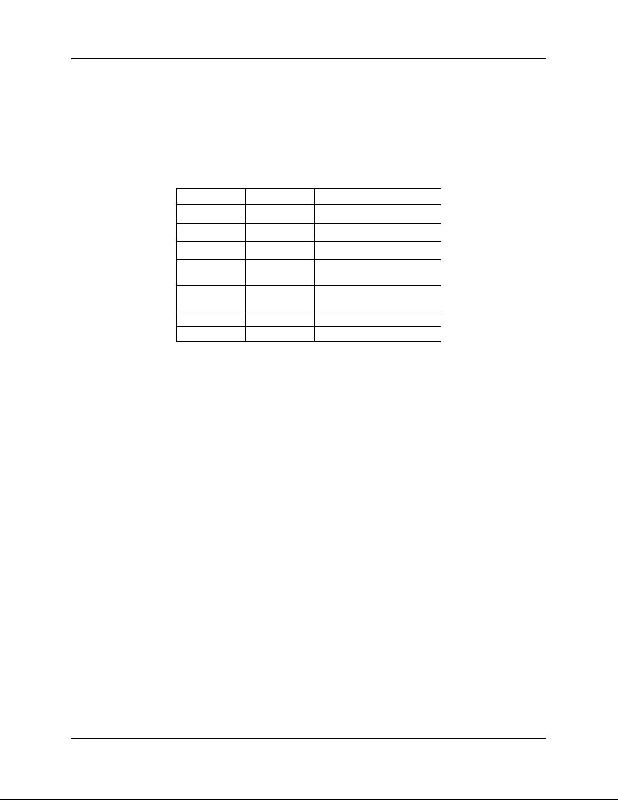
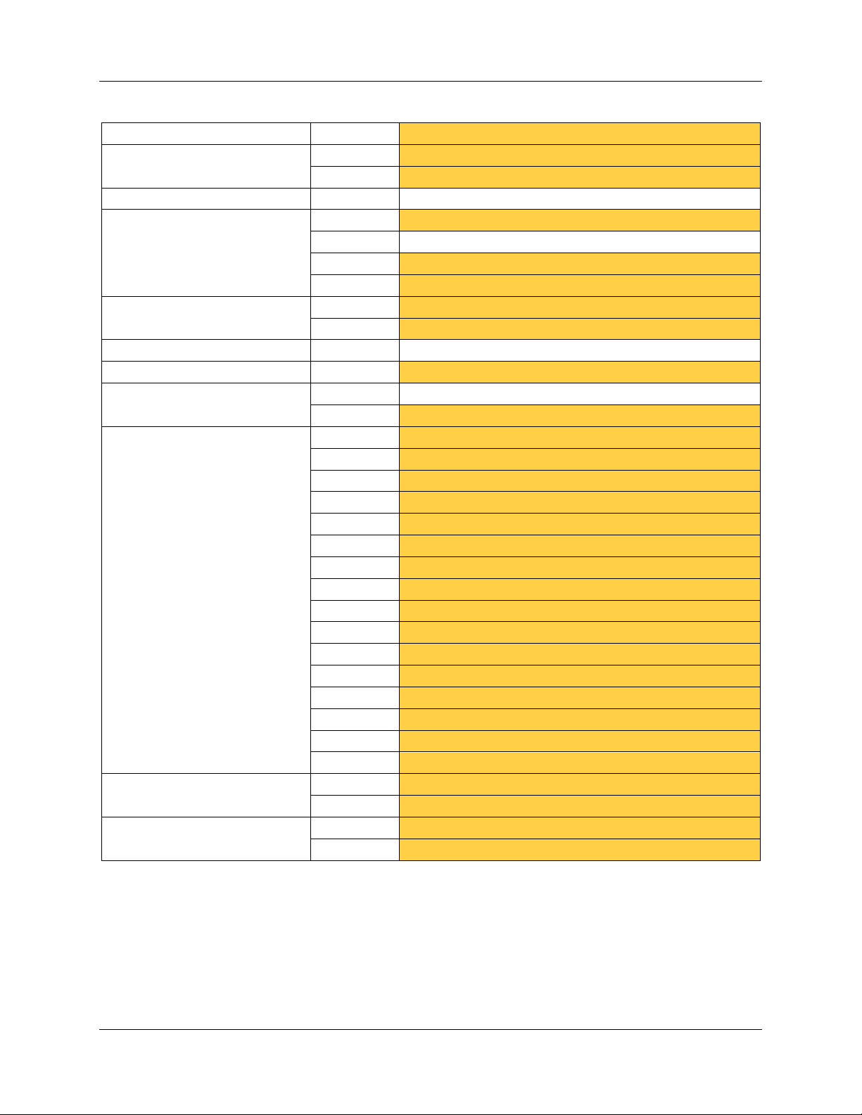
Shunt
NEUTRAL
LINE
A0
A3
750
1M 1M
1000pF
A1
1000pF
A2
LOAD
750
78M6613
V3P3
1
4
3
2
INLET
17
DIO14, 17
SAG, ALARM
6
XIN
XOUT
8
GNDA
GND
V3P3D
V3P3A
23
31
16
32
V3P3
TX
RX
UART_TX14
19
UART_RX
1 Introduction
This document describes the 6613_PSU_1+1S_URT_v1_00 firmware, which is used with the Teridian
78M6613 power and energy measurement IC. This firmware provides simple methods for calibration and
access to measurement data such as Instantaneous Power, Voltage, Current, Power Factor, and Line
Frequency. It is specifically optimized for measurement in single phase AC Power Supplies and
appliances with the following key features:
• Optimized for using current shunt resistors with analog input A0 configured as single-ended Voltage
input and input A1 configured as single-ended Current input. Inputs A2 and A3 unused.
• Phase error calibration routine included for maintaining accuracy over non-ideal power factors
(optional).
• Accumulation or averaging intervals based on fixed number of AC-cycles for compliance with latest
PMBus1.2 recommendations.
• Low-latency SAG status pin for sub-cycle AC fault detection.
• Dual mode host interface (Auto-Reporting or Command Line Interface).
All measurement calculations are computed by the 78M6613 and communicated to the host processor
over a serial interface (UART0) on the TX and RX pins of the 78M6613 device. Digital IOs utilized by this
firmware include:
• DIO17 is a SAG status pin updated every MUX cycle.
• DIO14 is a configurable alarm pin updated every accumulation interval.
Figure 1 shows a simplified connection diagram of the 78M6613 (emulator connections, decoupling
capacitors and 3.3VDC power supply are omitted in this diagram).
Figure 1: 78M6613 Simplified Connection Diagram for 6613_PSU_1+1S_URT_v1_00 Firmware
Rev. 1.0 5
Page 6
6613_PSU_1+1S_URT_V1_00 Firmware Description Document UG_6613_040
2 Measurement Description
2.1 Basic Measurement Equations
The Teridian 78M6613 with firmware 6613_PSU_1+1S_URT_v1_00 provides the user with measurement
data referred to as “Wideband” (WB). Wideband measurements are generally of interest when measuring
non-sinusoidal current/voltage, a typical condition in switched mode power supplies or similar systems.
Table 1: Measurement Equations Definitions
Symbol Parameter Wideband Equation
V RMS Voltage
I RMS Current
P Active Power
Q
S
PF Power Factor P/S
PA Phase Angle ACOS (P/S)
Reactive
Power
Apparent
Power
V = √∑
I = √∑
P = ∑
Q = √(S
S = V * I
The measurement outputs are continuously available to the user. To obtain measurement outputs, the
serial UART interface between the 78M6613 and the host processor must be set up and is described in
Section 3.
2.2 Sample Rate and Accumulation Interval
2
v(t)
2
i(t)
(i(t) * v(t))
2
– P2)
This firmware utilizes an effective sampling rate of 6554 samples per second for each input.
The values described in section 2.1 are calculated over a period commonly referred as accumulation
interval. The registers containing the measurements are updated at the completion of every accumulation
time. In firmware 6613_PSU_1+1S_URT_v1_00, the accumulation interval is based on multiples of the
Input Voltage AC cycle. For example if the accumulation interval is set to 30AC cycles, at 50Hz line
frequency, it will result in 20ms * 30 = 600ms. In this case the RMS values will be calculated over 3932
samples.
Accumulation interval can be changed in CLI mode by the following command (see Secti on 6 for details
of the CLI commands):
> ]18=+30 (Changes accumulation interval to 30 AC cycles)
6 Rev. 1.0
Page 7

UG_6613_ 040 6613_PSU_1+1S_URT_V1_00 Firmware Description Document
3 Serial Communication
The serial communication with the 78M6613 takes place over a UART (UART0) interface. The default
settings for the UART of the 78M6613, as implemented in this firmware, are given below:
Baud Rate: 38400bps
Data Bits: 8
Parity: None
Stop Bits: 1
Flow Control: Xon/Xoff
The firmware allows two types of communication protocols (modes) through UART0: CLI (Command Line
Interface) mode and auto-report mode (default operation).
4 Auto-reporting Mode
Upon application of 3.3VDC power, the 78M6613 will operate in Auto-reporting mode.
Data Packet : Auto-reported AC measurement data packet consisting of Voltage, Current, Watt, Power
Factor and Line Frequency send every accumulation cycle. Measurement data packet is send over
UART in ASCII format followed by line feed and carriage return.
Vrms Irms Watts PF Freq LF + CR
Measurement Parameter: The following table lists the measurement parameters and their respective bit
resolutions (LSB) that is sent over UART in ASCII format.
Measurement Parameter Resolution (LSB)
Voltage (Vrms) mV
Current (Irms) mA
Active Power(Watts) mW
Power Factor(PF) Range between 0 and 1000.
1000 indicative of 1.0 PF
Line Frequency(Freq) 0.01 Hz
5 Auto-reporting “Toggle” Command
To change from Auto-reporting mode to CLI mode (see Section 6 for details of the CLI mode), Ctrl Z
command must be sent from the host to the 78M6613 over the UART interface. A subsequent Ctrl Z
command will cause the 78M6613 to toggle back to Auto-Reporting mode.
Rev. 1.0 7
Page 8
6613_PSU_1+1S_URT_V1_00 Firmware Description Document UG_6613_040
6 Command Line Interfac e
The 6613_PSU_1+1S_URT_v1_00 firmware implements an instruction set called the Command Line
Interface (CLI), which facilitates communication via UART between the 78M6613 and the host processor.
6.1 Identification and Information Commands
The I command is used to identify the revisions of the 6613_PSU_1+1S_URT_v1_00 firmware code and
the embedded CE code. The host sends the I command to the 78M6613 as follows:
><CR>
The 78M6613 will reply the following:
TSC 78M6613 PSU 1+1S URT V1.00,Oct 15 2010(c) 2010 Teridian Semiconductor Corp.
All Rights Reserved
CEVI4ACF0
>
6.2 Reset Commands
A soft reset of the 78M6613 can be performed by using the Z command. The soft reset restarts code
execution at addr 0000 and does not alter flash contents. To issue a soft reset to the 78M6613, the host
sends the following:
>Z<CR>
The W command acts like a hardware reset. The energy accumulators in XRAM will retain their values.
Z Reset
Description: Allows the user to cause soft resets.
Usage: Z Soft reset.
W Simulates watchdog reset.
8 Rev. 1.0
Page 9

UG_6613_ 040 6613_PSU_1+1S_URT_V1_00 Firmware Description Document
6.3 MPU Data Access Command
All the measurement calculations are stored in the MPU data addresses of the 78M6613. The host
requests measurement information using the MPU data access command which is a right parenthesis
)
To request information, the host sends the MPU data access command, the address (in hex) which is
requested, the format in which the data is desired (Hex or Decimal) and a carriage return. The contents
of the addresses that would be requested by the host are contained in Section 7.
6.3.1 Individual Address Read
The host can request the information in hex or decimal format. $ requests information in hex, and ?
requests information in decimal. When requesting information in decimal, the data is preceded by a + or
a -. The exception is )AB? which returns a string (see Table 3, MPU location address 0xAB).
An example of a command requesting the measured power in Watts (located at address 0x08) in decimal
is as follows:
>)08?<CR>
An example of a command requesting the measured power in Watts (located at address 0x08) in hex is
as follows:
>)08$<CR>
6.3.2 Consecutive Read
The host can request information from consecutive addresses by adding additional ? for decimal or
additional $ for hex.
An example of requests for the contents in decimal of ten consecutive addresses starting with 0x12 is:
>)12??????????<CR>
An example of requests for the contents in hex of ten consecutive addresses starting with 0x12 would be:
>)12$$$$$$$$$$<CR>
Note: The number of characters per line is limited to no more than 60.
Rev. 1.0 9
Page 10

6613_PSU_1+1S_URT_V1_00 Firmware Description Document UG_6613_040
6.3.3 Block Reads
The block read command can also be used to read consecutive registers: )saddr:eaddr? For decimal
format or )saddr:eaddr$ for hex format where saddr is the start address and eaddr is the final address.
The following block read command requests the information contained in Table 2 in decimal format:
>)20:3D?<CR>
6.3.4 Concatenated Reads
Multiple commands can also be added on a single line. Requesting information in decimal from two
locations and the block command from above are given below:
>)12?)15?)20:3D?<CR>
Note: The number of characters per line is limited to no more than 60.
6.3.5 U Command
The U command is used for updating default values of the MPU Data permanently in the flash. Before
issuing the U command, CE must first be turned off by the disable CE command. An example of a U
command is as follows:
>)U
Additional examples of MPU Data Access commands are provided in the following table:
) MPU Data Access
Description: Allows user to read from and write to MPU data space.
Usage: ) {Starting MPU Data Address} {option}…{option}<CR>
Command
Combinations:
)saddr? <CR> Read the register in decimal.
)saddr?? <CR> Read two consecutive registers in decimal.
)saddr???<CR> Read three consecutive registers in decimal.
)saddr:eaddr?
Block read command in decimal format. Read
consecutive registers starting with starting
address saddr and ending with addres s eaddr.
Results given in decimal.
)saddr$<CR> Read the register word in h ex.
)saddr$$ <CR> Read two consecutive register words in hex.
)saddr$$$<CR> Read three consecutive register words in hex.
)saddr:eaddr$
Block read command in hex format. Read
consecutive registers starting with starting
address saddr and ending with addres s eaddr.
Results given in hex.
)saddr=n<CR> Write the value n to address saddr in hex format.
)saddr=n=m<CR> Write the values n and m to two consecutive
addresses starting at saddr in hex format.
)saddr=+n<CR> Write the value n to address saddr in decim al
format.
)saddr=+n=+m<CR> Write the values n and m to two consecutive
addresses starting at saddr in decimal format.
10 Rev. 1.0
Page 11

UG_6613_ 040 6613_PSU_1+1S_URT_V1_00 Firmware Description Document
)U<CR>
Updates the default values of the MPU Data
permanently in the flash.
Examples: )08$<CR> Reads data word at MPU address location 0x08
in hex format.
)08$$<CR> Reads data words at MPU address location
0x08, 0x09 in hex format.
)08$$$<CR> Reads data words at MPU address location
0x08, 0x09, 0x0A in hex format.
)28:4D$ Read data words in hex.
)08?<CR> Reads data word at MPU address location 0x08
in decimal format.
)08??<CR> Reads data words at MPU address location
0x08, 0x09 in decimal format.
)08???<CR> Reads data words at MPU address location
0x08, 0x09, 0x0A in decimal format.
)28:4D? Read data words at MPU a ddres s locatio n
starting 0x28 to 0x4D in decimal.
)04=12345678<CR> Writes 0x12345678 to MPU address location
0x04 in the hex format.
)04=12345678=9876ABCD<CR> Writes 0x12345678 to MPU address location
0x04 and 0x9876ABCD at MPU address location
0x05 in the hex format.
)04=+123<CR> Writes 123 to MPU address location 0x04 in the
decimal format.
)04=+123=-334<CR> Writes 123 to MPU address location 0x04 and
-334 to MPU address location 0x05 in the
decimal format.
Rev. 1.0 11
Page 12

6613_PSU_1+1S_URT_V1_00 Firmware Description Document UG_6613_040
6.4 Auxiliary Commands
6.4.1 Repeat Command
The repeat command can be useful for monitoring measurements and is efficient in demands from the
host.
If the host requests line frequency, alarm status, Irms wb overcurrent event count, Vrms SAG event
count, Vrms overvoltage event count, vo lta ge, po wer, and accumulated energy measurements with the
following command string:
>)20????????<CR>
If the host then desires this same request without issuing another command, the repeat command can be
used:
>, (no carriage return needed for the repeat command)
The host only needs to send one character rather than an entire string.
Auxiliary
Description: Various
Commands: , Typing a comma (“,”) repeats the command
issued from the previous command line. This is
very helpful when examining the value at a
certain address over time, such as the CE
DRAM address for the temperature.
/ The slash (“/”) is useful to separate comments
from commands when sending macro text files
via the serial interface. All characters in a line
after the slash are ignored.
12 Rev. 1.0
Page 13

UG_6613_ 040 6613_PSU_1+1S_URT_V1_00 Firmware Description Document
6.5 Calibration Commands
Using the precision source method, the user provides a precision voltage and precision current load to
the device for calibration. The 6613_PSU_1+1S_URT_v1_00 firmware provides commands to calibrate
the measurement units. For linear current sensors, such as current shunt, no phase calibration is
necessary.
There are two types of calibration commands. The first type provides complete calibration. The second
group, called atomic calibration commands, provides calibration for individual portions of the IC.
6.5.1 Complete Calibration Command (“Single Command Calibration”)
There are two calibration commands in this first group: CAL and CALW. Only one of these commands
is needed to calibrate the System/Unit.
To use these commands, a precision voltage source and a precision current source are required for the
calibration routine to use as a reference.
6.5.1.1 CAL Command
To use the CAL command, enter the following:
>CAL<CR>
The response is:
TCal OK
VCal OK:
ICal 0 OK:
>
The device would calibrate the temperature (adjust the Temperature Nominal MPU location 0xA6, saves
to flash and will initiate temperature gain compensation), calibrate the voltage (adjusts CAL VA and CAL
VB registers and saves them to flash), and finally calibrate the current (adjusts CAL IA register and saves
to flash).
6.5.1.2 CALW Command
To use the CALW command, enter the following:
>CALW<CR>
The response is:
TCal OK
VCal OK:
WCal 0 OK:
>
The device will calibrate the temperature, calibrate the voltage, and finally calibrate the power and save
all values to flash.
The commands are summarized in the following table:
CALx Complete Calibration Commands
Description: Allows the user to Calibrate the IC.
Usage: CAL Calibrates temperature, then voltage,
and finally current.
CALW Calibrates temperature, then voltage,
and finally power.
Rev. 1.0 13
Page 14

6613_PSU_1+1S_URT_V1_00 Firmware Description Document UG_6613_040
6.5.2 Atomic Calibration Commands
The atomic calibration commands provide individual calibration of voltage, current, temperature, watts
and a sequence of these results in providing full calibration for the unit.
6.5.2.1 CLV Command
An example of an atomic calibration command would be to calibrate voltage with the CLV command. The
CLV command calibrates voltage to the target value and tolerance and saves the coefficients to flash.
The CLV command example is given below:
>CLV<CR>
The response is:
VCal OK:
>
6.5.2.2 CLI Command
The user can then calibrate the current using the CLI1 command. The CLI1 command calibrates the
current to the target value and tolerance and saves the coefficients to flash. The CLI1 command example
is given below:
>CLI1<CR>
The response is:
ICal 0 OK:
>
6.5.2.3 CLP Command
The user can calibrate for phase added by a current transformer by using the CLP command. The CLP
command calibrates the phase to the target value and tolerance and saves the coefficient to flash. An
example of the procedure is given below.
Apply a controlled precision voltage and current signal at a set phase angle.
1. Enter target phase angle at )C3.
2. Enter phase tolerance at )BF
3. Enter phase calibration command.
>CLP<CR>
The response is
>PCal 1 OK:
14 Rev. 1.0
Page 15
UG_6613_ 040 6613_PSU_1+1S_URT_V1_00 Firmware Description Document
6.5.2.4 CLT Command
The CLT command is used for the temperature calibration. This command adjusts the Temperature
Nominal at MPU location 0xA6, saves to flash and will initiate temperature gain compensation. The CLT
command example is given below:
>CLT<CR>
The response is:
TCal OK
>
A summary of the atomic calibration commands are given in the table below:
CLxx Atomic Calibration
Commands
Description: Allows the user to Calibrate individual sections of the IC.
Usage: CLV Calibrates voltage only.
CLI1 Calibrate current only.
CLW1 Calibrate for power only.
CLP Calibrate for phase only.
CLT Calibrate temperature only.
The commands that follow are mainly for advanced users and are included for reference only.
6.6 CE Data Access Commands
The CE is the main signal processing unit in the 78M6613. The user writes to the CE data space are
mainly for calibration purposes. For the advanced user, details of CE data access commands are
described. The commands similar to the MPU access except that ] is used for the CE data access
command.
The host requests access to information from the CE data space using the CE data access command
which is a right bracket:
]
To request information, the host sends the CE data access command, the address location (in hex), the
format in which the data is desired (hex or decimal) and a carriage return. The contents of the addresses
that would be requested by the host are contained in Section 8.2.
The host can request the information in hex or decimal format. $ requests information in hex and ?
requests information in decimal.
6.6.1 Single Register CE Access
An example of a command requesting the calibration constant for current (located at address 0x08) in
decimal is as follows:
>]08?<CR>
An example of a command requesting the calibration constant for current (located at address 0x08) in hex
is as follows:
>]08$<CR>
Rev. 1.0 15
Page 16

6613_PSU_1+1S_URT_V1_00 Firmware Description Document UG_6613_040
6.6.2 Consecutive CE Reads
The host can request information from consecutive addresses by adding additional ? for decimal or
additional $ for hex.
An example of requests for the contents in decimal of ten consecutive addresses starting with 0x08 would be:
>]08??????????<CR>
An example of requests for the contents in hex of ten consecutive addresses starting with 0x08 would be:
>]08$$$$$$$$$$<CR>
Note: The number of characters per line is limited to 60 characters. Any character beyond the 60
character limit will be ignored by the CLI command interpreter.
6.6.3 CE Data Write
An example of a command writing to calibration constant for current (located at address 0x08) in decimal
is as follows:
>]08 = +16384 <CR>
An example of a command writing to calibration constant for current (located at address 0x08) in hex is as
follows:
>]08=4000 <CR>
6.6.4 U Command
The U command is used for updating default values of the CE Data permanently in the flash. Before
issuing the U command, CE must first be turned off by the disable CE command.
An example of a U command is as follows:
>CE0
>]U
Additional examples of CE Data Access commands are provided in the following table:
] CE Data Access
Description: Allows user to read from and write to CE data space.
Usage: ] {Starting CE Data Address}{option}…{option}<CR>
Command
Combinations:
]saddr?<CR> Read 32-bit word in decimal.
]saddr??<CR> R ead t wo consecutive 32-bit words in decimal.
]saddr???<CR> Read three consecutive 32-bit words in decimal.
]saddr$<CR> Read 32-bit words in hex.
]saddr$$<CR> R ead t wo consecutive 32-bit words in hex.
]saddr$$$<CR> Read thr ee consecutive 32-bit words in hex.
]U<CR> Update default version of CE Data in
FLASH. Important: The CE must be
stopped (CE0) before issuing this
command! Also, remember to restart
by executing the CE1 command prior to
attempting measurements.
16 Rev. 1.0
Page 17

UG_6613_ 040 6613_PSU_1+1S_URT_V1_00 Firmware Description Document
Examples: ]40$<CR> Reads CE data word at address location 0x40 in
the hex format.
]40$$<CR> Reads CE data word at address location 0x40
and 0x41 in the hex format.
]40$$$<CR> Reads CE data word at address location
0x40,0x41 and 0x42 in the hex format.
]40?<CR> Reads CE data word at address location 0x40 in
the decimal format.
]40??<CR> Reads CE data word at address location 0x40
and 0x41 in the decimal format.
]40???<CR> Reads CE data word at address location
0x40,0x42 and 0x43 in the decimal format.
]7E=12345678<CR> Writes 0x12345678 to CE address location 0x7E
in the hex format.
]7E=12345678=9876ABCD<CR> Writes 0x12345678 to CE address location 0x7E
and 0x9876ABCD to CE address location 0x7F
in the hex format.
]7E=+2255<CR> Writes 2255 to CE address location 0x7E in the
decimal format.
]7E=+2255=-456<CR> Writes 2255 to CE address location 0x7E and
-456 to CE address location 0x7F in the decimal
format.
Rev. 1.0 17
Page 18

6613_PSU_1+1S_URT_V1_00 Firmware Description Document UG_6613_040
The commands that follow are included for reference only.
6.7 CE Control Comma nds
The most pertinent command is the CE enable command, CEn. It is mainly used to turn the CE on or off.
The CE is normally enabled but in order to update the CE data entry to flash, the CE must first be turned
off using the CE0 command.
6.7.1 Disable CE Command
The CE can be disabled by using the following command:
>CE0<CR>
6.7.2 Turn On CE Command
The CE can be enabled by following command:
>CE1<CR>
Additional examples of CE Control Commands are provided in the following table:
C Compute Engin e Control
Description: Allows the user to enable and configure the compute engine.
Usage: C {option} {argument}<CR>
Command
Combinations:
Examples: CE0<CR> Disables the CE.
CEn<CR> Compute Engine Enable (1 Enable,
0 Disable)
CTn<CR> Select input n for TMUX output pin. Enter n in hex
notation.
CREn<CR> RTM output control (1 Enable, 0 Disable)
CRSa.b.c.d<CR> Selects CE addresses for RTM output. (maximum
of four).
CE1<CR> Enables the CE.
CT1E<CR> Selects the CE_BUSY signal for the TMUX output
pin.
18 Rev. 1.0
Page 19

UG_6613_ 040 6613_PSU_1+1S_URT_V1_00 Firmware Description Document
(hex)
Temperature difference from 22° C.
7 MPU Measurement Outputs
This section describes the measurement outputs that can be obtained in Manual CLI Mode. Energy
outputs are accumulated numbers. The host accessing the measurement information from the 78M6613
more frequently than the accumulation interval will not result in any update in the information.
Table 2 lists the wideband measurement outputs.
Table 2: MPU Outputs
Output
Delta
Temperature
Line
Frequency
Alarm Status 22
Irms A
Overcurrent
Event Count
Location
20 0.1 °C
21 0.01 Hz Line Frequency
23
LSB Comment Example
Definition for Status Register
Bit 0: Minimum Temperature Alarm.
Bit 1: Maximum Temperature Alarm.
Bit 2: Minimum Frequency Alarm.
Bit 3: Maximum Frequency Alarm.
Bit 4: SAG Voltage Alarm.
Bit 5: MINVA
voltage on VA input.
Bit 6: MAXVA
voltage on VA input.
Bit 7: Reserved.
Bit 8: MAXIA WB
current exceeded.
Bit 9: Reserved.
Bit 10: Reserved.
Bit 11: PFA negative WB - Power
Factor Negative Threshold Alarm.
Only available if )F2 bit 2 is 1.
Bit 12: PFA positive WB
Factor Positive Threshold Alarm.
Bits 13 - 20: Reserved.
Bit 21 – CREEP Alert.
Bit 22 - 31: Reserved.
Counter increments on each edge
– under minimum
– over maximum
– maximum WB
– Power
event.
If external temperature is 32 °C
)20?<CR>
Returns:
+10.0
If the line frequency is 60 Hz:
)21?<CR>
Returns:
+60.00
Alarms become “1” when
thresholds exceeded.
Note: Additional Status Alert is
Located at addr 0xBD (see Table 3)
Note: When AC voltage input is less
than or equal to 10 V
• Only MINVA alarm is active.
• All measurements are forced
to 0 except power factor,
which is forced to 1.
Note: The frequency measurement
is forced to 0 as long as the SAG
voltage alarm is active.
If four over current events have
occurred:
)23?<CR>
Returns: +4
RMS
,
Rev. 1.0 19
Page 20

6613_PSU_1+1S_URT_V1_00 Firmware Description Document UG_6613_040
+120.000
Output
Vrms Under
Voltage
Event Count
Vrms Over
Voltage
Event Count
Vrms A 26 mV Vrms voltage
Watts A 27 mW
Wh A 28 mWh
Total Cost A 29 mUnits Cost of Wh A.
Irms A 2A mA rms current measurement.
VARs A 2B mW
Location
(hex)
24
25
LSB Comment Example
If four under voltage events have
Counter increments on each edge
event.
If four over voltage events have
Counter increments on each edge
event.
If the line voltage is 120 V
If 120 Watts are measured
Active power measurement (per
second).
Active accumulated energy
measurement (per hour).
If the cost is 102.536 units
Reactive power measurement (per
second).
occurred:
)24?<CR>
Returns: +4
occurred:
)25?<CR>
Returns: +4
)26?<CR>
Returns:
+120.000
)27?<CR>
Returns:
+120.000
If 120 Wh are measured
)28?<CR>
Returns:
+120.000
)29?<CR>
+102.536
If current measured
is 12 Amps
)2A?<CR>
Returns:
+12.000
If 120 VARs
are measured
)2B?<CR>
Returns:
If 120 VAs
are measured
)2C?<CR>
Returns:
+120.000
If the power factor
is 0.95
)2D?<CR>
Returns:
+0.950
degrees
)2E?<CR>
Returns:
+60.000
VAs A 2C mW
Power
Factor A
Phase
Angle A
2D
2E
–
–
Apparent power measurement (per
second).
Power factor. The output will be
between -0.950 and 1.000.
Positive power factor is defined as
current lagging voltage (inductive).
Negative power factor is defined as
voltage lagging current
(capacitive).
If the phase angle measured is 60
Phase angle. The output will be
between 180.000 and -180.000.
20 Rev. 1.0
Page 21

UG_6613_ 040 6613_PSU_1+1S_URT_V1_00 Firmware Description Document
Output
Reserved 2F
Vrms A Min 30 mV Minimum Vrms measur e d
Vrms A Max 31 mV Maximum Vrms measured
Watts A Min 32 mW
Watts A Max 33 mW
Irms A Min 34 mArms Minimum rms current measured.
Irms A Max 35 mArms Maximum rms current measured.
VARs A Min 36 mW
VARs A Max 37 mW
VAs A Min 38 mW
Location
(hex)
LSB Comment Example
–
Reserved
If the minimum line voltage
If the maximum line voltage
If the minimum power measured
Minimum active power measured
(per second)
If the maximum power measured
Maximum active power measured
(per second)
If the smallest current measured is
If the largest current measured is
If the largest VARs measured
Minimum reactive power measured
(per second).
If the largest VARs measured
Maximum reactive power
measured (per second).
If the smallest VAs measured
Minimum apparent power
measured (per second).
Reserved
measured was 105 V
)30<CR>
Returns:
+105.000
measured was 130 V
)31<CR>
Returns:
+130.000
is 80 Watts
)32?<CR>
Returns:
+80.000
is 200 Watts
)33?<CR>
Returns:
+200.000
1 Amp
)34?<CR>
Returns:
+1.000
30 Amps
)35?<CR>
Returns:
+30.000
is 80 VARs
)36?<CR>
Returns:
+80.000
is 300 VARs
)37?<CR>
Returns:
+300.000
is 80 VARs
)38?<CR>
Returns:
+80.000
Rev. 1.0 21
Page 22

6613_PSU_1+1S_URT_V1_00 Firmware Description Document UG_6613_040
Output
VAs A Max 39 mW
Power
Factor A Min
Power
Factor A
Max
Phase
Angle A Min
Phase
Angle A Max
Reserved 3E
Reserved 3F
Location
(hex)
3A
3B
3C
3D
LSB Comment Example
If the largest VAs measured
is 300 VARs
)39?<CR>
Returns:
+300.000
is –0.6
)3A?<CR> Returns:
-0.600
is 0.9
)3B?<CR> Returns:
+0.900
measured is 10 degrees
)3C?<CR>
Returns:
+10.000
measured is 70 degrees
)3D?<CR>
Returns:
+70.000
Reserved
Reserved
–
–
–
–
–
–
Maximum apparent power
measured (per second).
Minimum power factor measured.
Minimum is defined as the most
negative or least positive number.
Maximum power factor measured.
Maximum is defined as the most
positive or least negative number.
Minimum phase angle measured.
Maximum phase angle measured.
Reserved
Reserved
If minimum power factor measured
If maximum power factor measured
If the minimum phase angle
If the maximum phase angle
22 Rev. 1.0
Page 23

UG_6613_ 040 6613_PSU_1+1S_URT_V1_00 Firmware Description Document
8 Configuration Paramet e r E ntry
8.1 MPU Parameters
Table 3 lists the MPU parameters configurable by the 6613_PSU_1+1S_URT_v1_00 Firmware.
Table 3: MPU Parameters
MPU
Parameter
VMAX A A0 mVrms +471.500
Starting IA A1 mArms +0.007
IMAX A A2 mArms +52.000
Unused A3 - A5 – – Unused
Temperature
Nominal
Reserved A7 – – Reserved
PPMC A8 ppm/°C -668 ppm per °C.
PPMC2 A9
Location
(hex)
A6 – +0
LSB Default Comment Example
ppm/°C
2
-341
External rms voltage
corresponding to 250 mVpk at the
VA input of the 78M6613. It must
be set high enough to account for
overvoltages. Usually set to
471.500 V (471.500d).
Minimum current value to be
measured on the IA input.
Currents below this value will be
ignored. Also known as CREEP
IA.
External rms current
corresponding to 250 mVpk at the
IA input of the 78M6613.
Temp_raw_x reading at 22 °C.
Needed to enable temperature
compensation.
ADC temperature compensation
ppm per °C2.
If only using a 120V
system, the user can set
VMAX A to about 2x the
maximum voltage for added
resolution. Set VMAX A to
)A0=+270.000<CR>
Default setting is 7 mA. If
start current on channel A
desired is 10 mA:
)A1=+0.010<CR>
The default is set to 52
Amps for overhead. For
added margin, in a system
using current shunts IMA X
could be changed as
IMAX= (Vpk/√2)/R
For a 4 mΩ current shunt
IMAX=44.19 Amps
To set IMAX A:
)A2=+44.190<CR>
Temp _raw_x is obtained
from the CE:
]71?<CR>
This value is then entered
)A6=+value in decimal
Also, the command:
>CLT<CR>
Will do the same as the
steps above.
Do not change the default
Do not change the default
270V:
follows:
here:
setting.
setting.
shunt
Rev. 1.0 23
Page 24

6613_PSU_1+1S_URT_V1_00 Firmware Description Document UG_6613_040
–
MPU
Parameter
Cost/kWh AA mUnits +0.150
Units of Cost AB N/A USD
Reserved A0 - BC – 0 Reserved Reserved
Additional
Status
Unused BE
Tolerance on
Phase
Reserved C0 – 0 Reserved Reserved
Calibration
Voltage
Location
(hex)
BD – 1
BF 0.001° 0.100°
C1 mVrms +120.000
LSB Default Comment Example
Cost per kWh (kilowatt hour) in
milliunits.
4-byte string describing unit of
cost
(e.g. USD, EURO etc.). There
must be 4 characters. If entering
US dollars, USD, there needs to
be a space after the D to make it a
four character string.
Bit 0 – Reserved.
Bit 1 – WPULSE Disable.
Bit 2 – VCal Failure.
Bit 3 – ICal1 Failure.
Bit 4 – WCal1 Failure.
Measured value to fall within this
set tolerance of the target value
(Calibration Current entry) for the
calibration to be complete.
Target line voltage (rms) used for
calibration.
If the cost per kWh is to be
10 units:
)AD=+10.000<CR>
To enter US Dollars:
)AB=”USD “<CR>
To enter Euros:
)AB=”EURO”<CR>
If the tolerance to the target
phase is desired to be more
coarse, to within 0.5°, the
user can enter the
following:
>)BF=+0.500<CR>
If the target line voltage for
calibration is 220V, enter
the following:
>)C1=+220<CR>
24 Rev. 1.0
Page 25

UG_6613_ 040 6613_PSU_1+1S_URT_V1_00 Firmware Description Document
MPU
Parameter
Calibration
Current
Calibration
Phase
Tolerance on
Voltage
Tolerance on
Current
Average
Count for
Voltage
Average
Count for
Current
Max Iteration
for Voltage
Max Iteration
for Current
Location
(hex)
C2 mArms +1.000
C3 0.1° +0
C4 mVrms +0.010
C5 mArms +0.010
C6 1 +3
C7 1 +3
C8 1 +10
C9 1 +10
LSB Default Comment Example
Target load current (rms) used for
calibration.
Target Phase (voltage to current).
Normally set to zero.
Measured value to fall within this
set tolerance of the target value
(Calibration Voltage entry) for t he
calibration to be complete.
Measured value to fall within this
set tolerance of the target value
(Calibration Current entry) for the
calibration to be complete.
Number of voltage measurements
taken and averaged to be
compared to the target value
(Calibration Voltage entry).
Number of current measurements
taken and averaged to be
compared to the target value
(Calibration Current entry).
Number of attempts to reach the
target value (Calibration Voltage
entry) within the programmed
tolerance.
Number of attempts to reach the
target value (Calibration Voltage
entry) within the programmed
tolerance.
If the target load current for
calibration is 2A, enter the
following:
>)C2=+2<CR>
If the tolerance to the target
voltage is desired to be
more coarse, to within
0.1V, the user can enter the
following:
>)C4=+0.100<CR>
If the tolerance to the target
current is desired to be
more coarse, to within
0.1A, the user can enter the
following:
>)C5=+0.100<CR>
If the amount of averaging
for the voltage
measurement is desired to
increase to 10 enter the
following:
>)C6=+10<CR>
If the amount of averaging
for the current
measurement is desired to
increase to 10 enter the
following:
>)C7=+10<CR>
If maximum number of
iterations to be tried for
obtaining the target value of
voltage within the set
tolerance (at C4) is to be
reduced to 5, then enter:
>)C8=+5<CR>
If maximum number of
iterations to be tried for
obtaining the target value of
power within the set
tolerance (at C5) is to be
reduced to 5, then enter:
>)C9=+5<CR>
Rev. 1.0 25
Page 26

6613_PSU_1+1S_URT_V1_00 Firmware Description Document UG_6613_040
MPU
Parameter
Tolerance on
Watts
Average
Count for
Watts
Max Iteration
for Watts
Calibration
WRATE
Calibration
Temperature
Calibration
Watts
Temp Alarm
Min Threshold
Temp Alarm
Max
Threshold
Location
(hex)
CA mW +0.010
CB 1 +3
CC 1 +10
CD 1 +6350
CE 0.1°C +22.0
CF
D0 0.1°C +0.0°C
D1 0.1°C +70°C
LSB Default Comment Example
mW
Measured value to fall within this
set tolerance of the target value
(Calibration Voltage multiplie d by
the calibration current entries) for
the calibration to be complete.
Measured value to fall within this
set tolerance of the target value
(Calibration Voltage multiplie d by
the calibration current entries) for
the calibration to be complete.
Number of attempts to reach the
target value (Calibration Voltage
multiplied by the calibration
current entries) within the
programmed tolerance.
Entry for WRATE during the
calibration step only. After
calibration, WRATE returns to the
value entered in ]0F.
Target nominal temperature for
calibration.
120.000 Target Watts used for calibration.
Minimum Temperature Alarm
Threshold. A temperature below
this threshold will set the alarm
(bit 0 of the Alarm Status
Register).
Maximum Temperature Alarm
Threshold. A temperature above
this threshold will set the alarm
(bit 1 of the Alarm Status
Register).
If the tolerance to the target
power is desired to be more
coarse, to within 0.1W, the
user can enter the
following:
>)CA=+0.100<CR>
If the amount of averaging
for the power measurement
is desired to increase to 10
enter the following:
>)CB=+10<CR>
If maximum number of
iterations to be tried for
obtaining the target value of
power within the set
tolerance (at CA) is to be
reduced to 5, then enter:
>)CC=+5<CR>
If the user desires the
target nominal temperature
to be 25°C, then set as
follows:
>)CE=+25.0<CR>
If the target Watts for
calibration is 240, enter the
following:
>)CF=+240.000<CR>
If the minimum temperature
threshold is to be change to
10°C then set as follows:
>)D0=+10.0
If the maximum
temperature threshold is to
be change to 50°C then set
as follows:
>)D1=+50.0
26 Rev. 1.0
Page 27

UG_6613_ 040 6613_PSU_1+1S_URT_V1_00 Firmware Description Document
If the peak current
MPU
Parameter
Frequency
Minimum
Threshold
Frequency
Maximum
Threshold
SAG Voltage
Alarm
Threshold
Min Voltage
Alarm
Threshold
Peak Voltage
Alarm
Threshold
Unused D7-D8 –
Location
(hex)
D2 0.01Hz +59.00
D3 0.01Hz +61.00
D4 mVpk +80.0
D5 mVrms +100.000
D6 mVrms +140.000
LSB Default Comment Example
Minimum Frequency Alarm
Threshold. A frequency below
this threshold will set the alarm
(bit 2 of the Alarm Status
Register).
Maximum Frequency Alarm
Threshold. A frequency above
this threshold will set the alarm
(bit 3 of the Alarm Status
Register).
Sets an alarm (bit 4 of the Alarm
Status Register) if voltage drops
below the SAG threshold.
Minimum voltage level selected to
flag user (bit 5 of the Alarm Status
Register).
Peak voltage setting that user
wishes to flag (bit 6 of the Alarm
Status Register).
If the minimum frequency
threshold is to be changed
to 59.50 Hz then enter the
following:
>)D2=+59.50
If the maximum frequency
threshold is to be changed
to 60.50 Hz then enter the
following:
>)D2=+60.50
To change the minimum
voltage threshold from the
40 Volt default to 80 Volts:
)D5=+80.000<CR>
To change the peak voltage
threshold from the default
407.3 Volts to 280 Volts:
)D6=+280.000<CR>
Peak IA
Alarm
Threshold
D9 mArms +15.000
Maximum Current measured on
the IA channel above which a flag
must set (bit 8 of the Alarm Status
Register).
threshold is to be changed
from the default value of 15
Amps to 30 Amps then set
as follows:
)D9=+30.000<CR>
Rev. 1.0 27
Page 28

6613_PSU_1+1S_URT_V1_00 Firmware Description Document UG_6613_040
MPU
Parameter
Unused DA - DB –
PFA_ Neg
Threshold
PFA_ Pos
Threshold
Unused DE - DF – – Unused
Unused E0 - E5 – – Unused
Alarm
Mask_Reg
Alarm
Mask_DIO
AC Cycle
Count for CAL
Reserved F0 – 0 Reserved Reserved
Location
(hex)
DC – -0.700
DD – +0.700
E6
E7 – 00201FFF
EF 1 30 Number of AC cycles to average
LSB Default Comment Example
Power Factor Negative Threshold.
A less negative power factor than
this threshold will set an alarm (bit
11 of the Alarm Status Register).
Only available if )F2 bit 2 is set to
1.
Power Factor Positive Threshold.
A positive power factor less than
this threshold will set an alarm (bit
12 of the Alarm Status Register).
Alarm mask for bits in the Alarm
–
00201FFF
Status register. A “0” masks the
alarm from the register bit.
Alarm mask for an alarm pin
(DIO20). A “0” masks the alarm
from DIO20
during calibration
If the negative power factor
threshold is to be changed
from the default to -0.6 then
set as follows:
)DC=-0.600<CR>
If the positive power factor
threshold is to be changed
from the default to +0.6
then set as follows:
)DD=+0.600<CR>
If bits 0 and 1 are to be
masked then set as follows:
>)E6=00801FFC
Alarm mask for an alarm
pin (DIO20). A “0” masks
the alarm from DIO20
Min/Max
Control
Clear Control
and Power
Factor Polarity
F1
F2 – 0
–
BIT1 – 1 Start/Stop MIN/MAX
recording.
1 = Start
0
0 = Stop
BIT0 – 1 Reset MIN/MAX
registers before recording. Bit
autoclears.
Clear Control and Power Factor
Polarity Register:
Bit 2 – Power Factor Polarity
0 = Power Factor is
positive only. Negative alarm
thresholds and alarms are not
enabled.
1 = Power factor can be
positive or negative.
Bit1 – Clears Counts
Bit 0 – Clears Accumulators.
Reset & Start MIN/MAX
Stop MIN/MAX recording
recording.
)F1=3<CR>
)AC=00<CR>
28 Rev. 1.0
Page 29

UG_6613_ 040 6613_PSU_1+1S_URT_V1_00 Firmware Description Document
8.2 CE Parameters
Table 4 lists the CE parameters configurable by the 6613_PSU_1+1S_URT_v1_00 Firmware. The user
does not need to alter any of these parameters.
Table 4: CE Parameters
CE
Parameter
CAL IA 08
Unused 09
CAL VA 0A
Unused 0B
PHASE_
ADJ_IA
Unused 0D
CESTATE 0E 5001h
Location(
hex)
0C
LSB Default Comment Example
16384 is
the default
and is a
gain of 1.
32767 is
max giving
a gain of
2.
16384 is
the default
and is a
gain of 1.
32767 is
max giving
a gain of
2.
-16384 ≤
PHASE_A
DJ_IA ≤
+16384
+13873
+16384
0
Gain constant for IA
Gain constant for
Phase adjustment
PHASE_ADJ_IA *
-14
2
SAG CNT
Bits 15:8 –
determines the
consecutive voltage
samples below
SAG_Threshold
before a sag alarm
is declared. 255 is
the maximum
Pulse gain factor
Bits 1 an d 0
01 – (6/64)x
11 – 1.5x
input.
VA input.
=15 *
(degrees)
value.
00 – 6x
10 – 96x
If current on channel A is low by 1%
scale the nominal number, 16384 by
1/(1-0.01). Number to be entered would
be 16549:
]08=+16549<CR>
If current on channel A is high by 1%
scale the nominal number, 16384 by
1/(1+0.01). Number to be entered would
be 16222:
]08=+16222<CR>
If voltage on channel A is low by 1%
scale the nominal number, 16384 by
1/(1-0.01). Number to be entered would
be 16549:
]0A=+16549<CR>
If current on channel A is high by 1%
scale the nominal number, 16384 by
1/(1+0.01). Number to be entered would
be 16222:
]0A=+16222<CR>
No adjustment should be necessary
when using current shunts.
]0E=5001
Selects at least 80 (50h) c onsecutive
voltage samples below SAG_Threshold
before SAG alarm.
Selects Pulse Gain Factor equal to 6/64
(1h)
Rev. 1.0 29
Page 30

6613_PSU_1+1S_URT_V1_00 Firmware Description Document UG_6613_040
CE
Parameter
WRATE 0F
Reserved 10 Reserved
SAG
Threshold
QUANTA 12
Unused 13-15
QUANT IA 16
Location(
hex)
11
LSB Default Comment Example
Kh =
VMAX A *
IMAX A /
(WRATE *
X)
1.6826E+0
1 WattSec
VMAX A
*4.2551E-
07 (Vpk)
+4860
+168225
Controls the
number of pulses
that are generated
per measured Wh
and VARh
measurements.
The voltage
threshold for SAG
warnings. The
default value is 80
Vpk if VMAX = 600
Kh = 0.32 * Wh / pulse wi th X = 6/64,
]0F=+4860
VMAX =600 V
IMAX = 52 A
]11=+313350
80 Vpk SAG Threshold.
V.
Compensation
VMAX A *
IMAX A *
1.8541E-
10 (Watt)
0
added to the Watt
calculation. Used
for compensation at
low current levels.
Keep below
10000d.
IA input
compensation
added for input
noise and
truncation in the
squaring calculation
2
. Used for
for I
(A
2
*
2
)
(IMAX A)
4.6351E-11
0
compensation at
low current levels.
Keep below
10000d.
and
Unused 17
Number of AC
AC Cycle
Count
18 1 +4
cycles for
accumulation
interval (min=4)
To changes accumulation interval to 10
Note: Set value of AC cycles between 4
and 100/120 (for 50/60Hz respectively).
AC cycles:
]18=+10<CR>
To increase all channels equally by 1%
scale the nominal number, 16384 by
1/(1-0.01). Number to be entered would
be 16549:
]19=+16549<CR>
Gain Adjust 19
16384 is
the default
and is a
gain of 1.
+16384
32767 is max giving
a
gain of 2.
To decrease all channels 1% scale the
nominal number, 16384 by 1/(1+0.01).
Number to be entered would be 16222:
]19=+16222<CR>
Reserved 1A-1B – – Reserved
Reserved
30 Rev. 1.0
Page 31
UG_6613_ 040 6613_PSU_1+1S_URT_V1_00 Firmware Description Document
9 Address Content Summary
Table 5: MPU Output Summary Chart
Address Output
Common Data 20 Delta Temp
21 Line Frequency
22 Alarm Status
23 Over Current Event Count
24 Under Voltage Event Count
25 Over Voltage Event Count
26 Volts
27 Watts (A)
28 Energy (A)
29 Cost (A)
Wideband Data 2A Current (A)
2B VAR (A)
2C VA (A)
2D Power Factor (A)
2E Phase (A)
2F (Reserved for Future)
Min/Max Data 30 Vrms Min
31 Vrms Ma x
32 Watts Min (A)
33 Watts Max (A)
34 Current Min (A)
35 Current Max (A)
36 VAR Min (A)
37 VAR Max (A)
38 VA Min (A)
39 VA Max (A)
3A Power Factor Min (A)
3B Power Factor Max (A)
3C Phase Min (A)
3D Phase Max(A)
3E (Reserved for Future)
3F (Reserved for Future)
Rev. 1.0 31
Page 32
6613_PSU_1+1S_URT_V1_00 Firmware Description Document UG_6613_040
Table 6: MPU Input Summary Chart
Voltage
Current
Unused
Temperature
Cost
Reserved
Misc. Config
Unused
Quick Calibration Parameters
Temperature
Frequency
A0
A1
A2 Imax (A)
A3 - A5 Unused
A6
A7 Reserved
A8 PPMC
A9 PPMC2
AA
AB Cost Unit s tring
AC - BC
BD
BE Unused
BF Tolerance on Phase Calibration
C0
C1 Calibration Voltage (Target)
C2 Calibration Current (Target)
C3 Calibration Phase
C4 Tolerance on Voltage Calibration
C5 Tolerance on Current Calibration
C6 Average Count for Voltage
C7 Average Count for Current
C8 Max Iterations for Voltage
C9 Max Iterations for Current
CA Tolerance on Watts Calibration
CB Average Count for Watts
CC Max Iterations for Watts
CD Calibration WRATE
CE Calibration Temperature
CF Calibration Watts (Target)
D0
D1 Max Temperature Alarm Threshold
D2
D3 Max Frequency Alarm Threshold
Vmax
Imin (Creep A)
TEMPERATURE NOMINAL
Cost per KWh
Reserved
Configuration
Calibration Type
Min Temperature Alarm Threshold
Min Frequency Alarm Threshold
32 Rev. 1.0
Page 33
UG_6613_ 040 6613_PSU_1+1S_URT_V1_00 Firmware Description Document
Voltage
Unused
Current
Power Factor
Unused
Unused
Alarm Mask for Status Regs
Alarm Mask for Alarm DI/O
AC Cycle Count for CAL
Reserved
Min/Max Controls
Clear Control
D4
D5 Min Voltage Alarm Threshold
D6 Max Voltage Alarm Threshold
D7 Unused
D8
D9 Max Current Alarm Threshold
DA
DB
DC Power Factor Alarm - Threshold
DD Power Factor Alarm + Threshold
DE-DF Unused
E0 – E5 Unused
E6
E7
EF AC Cycle Count for Calibration.
F0
F1
F2
SAG Voltage Alarm Threshold
Unused
Unused
Unused
Alarm Mask for Status
Alarm Mask for Alarm DIO
Reserved
Min/Max Controls
Accumulator and Counter Clear. Power Factor Polarity
Table 7: CE Input Summary Chart
Calibration
Phase Compensation
CE Configuration
Pulse Rate
SAG Threshold
Quantization Corrections
Accumulation Interval
Gain Adjust
08
09 Unused
0A Calibration Gain VA
0B Unused
0C
0D Unused
0E
0F
10 Reserved
11
12
13-15 Unused
16 Quantization offset IA
17 Unused
18
19
Calibration Gain IA
Phase Adjust IA
CE State
WRATE
SAG Threshold
Quantization offset Watts
AC Cycle Count for Accumulation Interval
Temperature Gain Adjust
Rev. 1.0 33
Page 34

6613_PSU_1+1S_URT_V1_00 Firmware Description Document UG_6613_040
10 Digital IOs
DIO17 is a dedicated SAG status pin that is set high when SAG Voltage alarm triggers. SAG Voltage
alarm status is checked every MUX cycle for low latency detection of AC fault conditions. Both the
instantaneous voltage alarm threshold and sample count for the SAG alarm are configurable. See CE
STATE and SAG Threshold registers for more information.
DIO14 is a configurable alarm pin that is an ‘OR function’ of several mask-able alarm bits. The alarm
status is checked and updated following an update of the measurement output registers (once every
Accumulation cycle). See registers E6 and E7 for mask settings.
11 Contact Information
For more information about Maxim products or to check the availability of the 78M6613, contact technical
support at www.maxim-ic.com/support.
34 Rev. 1.0
Page 35

UG_6613_ 040 6613_PSU_1+1S_URT_V1_00 Firmware Description Document
Document Revision His t ory
Version Date History
1.0 10/29/2010 First publication.
Rev. 1.0 35
 Loading...