

Page 1
PART TEMP RANGE
MAX TEMPCO
(ppm/°C)
INITIAL ERROR
(mV)
PIN-PACKAGE
PKG
CODE
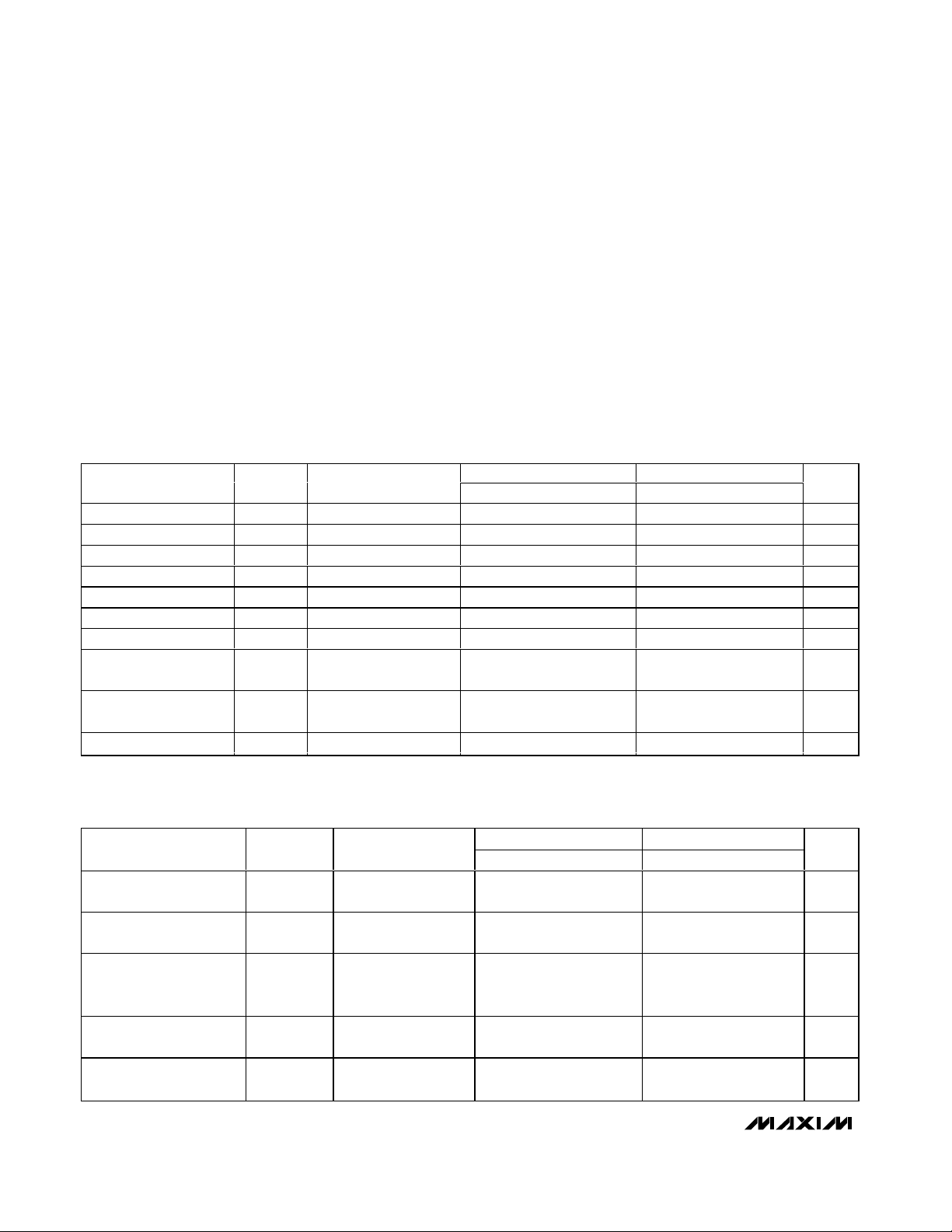
REF01EP 0°C to +70°C 8.5 ±30 8 Plastic DIP P8-2
REF01EP+ 0°C to +70°C 8.5 ±30 8 Plastic DIP P8-2
REF01HP 0°C to +70°C 25 ±50 8 Plastic DIP P8-2
REF01HP+ 0°C to +70°C 25 ±50 8 Plastic DIP P8-2
REF01HSA 0°C to +70°C 25 ±50 8 SO S8-2
REF01HSA+ 0°C to +70°C 25 ±50 8 SO S8-2
REF01CP 0°C to +70°C 65 ±100 8 Plastic DIP P8-2
REF01CP+ 0°C to +70°C 65 ±100 8 Plastic DIP P8-2
REF01CSA 0°C to +70°C 65 ±100 8 SO S8-2
REF01CSA+ 0°C to +70°C 65 ±100 8 SO S8-2
REF01CESA -40°C to +85°C 65 ±100 8 SO S8-2
REF01CESA+ -40°C to +85°C 65 ±100 8 SO S8-2
General Description
The REF01/REF02 are industry-standard precision voltage references. The stable 10V output of the REF01
can be adjusted over a ±6% range with minimal effect
on temperature stability. The 5V output REF02 can also
be adjusted over a ±6% range. The 10V REF01 has a
single-supply operation over an input voltage range of
13V to 33V, while the 5V REF02 has a single-supply
operation over an input voltage range of 7V to 33V.
Both devices offer a low-current drain of 1mA. The
REF02 also provides a TEMP pin whose output voltage
varies linearly with temperature, making this device
suitable for a wide variety of temperature-sensing and
control applications. For new designs, refer to the
MAX6035 or MAX6143 data sheets.
Features
♦ Pretrimmed to +5V, +10V
♦ Excellent Temperature Stability: 3ppm/°C (typ)
♦ Low Noise: 10µV
P-P
(REF02)
♦ Short-Circuit Protected
♦ Linear Temperature Transducer Output (REF02)
REF01/REF02
+5V, +10V Precision
Voltage References
________________________________________________________________ Maxim Integrated Products 1
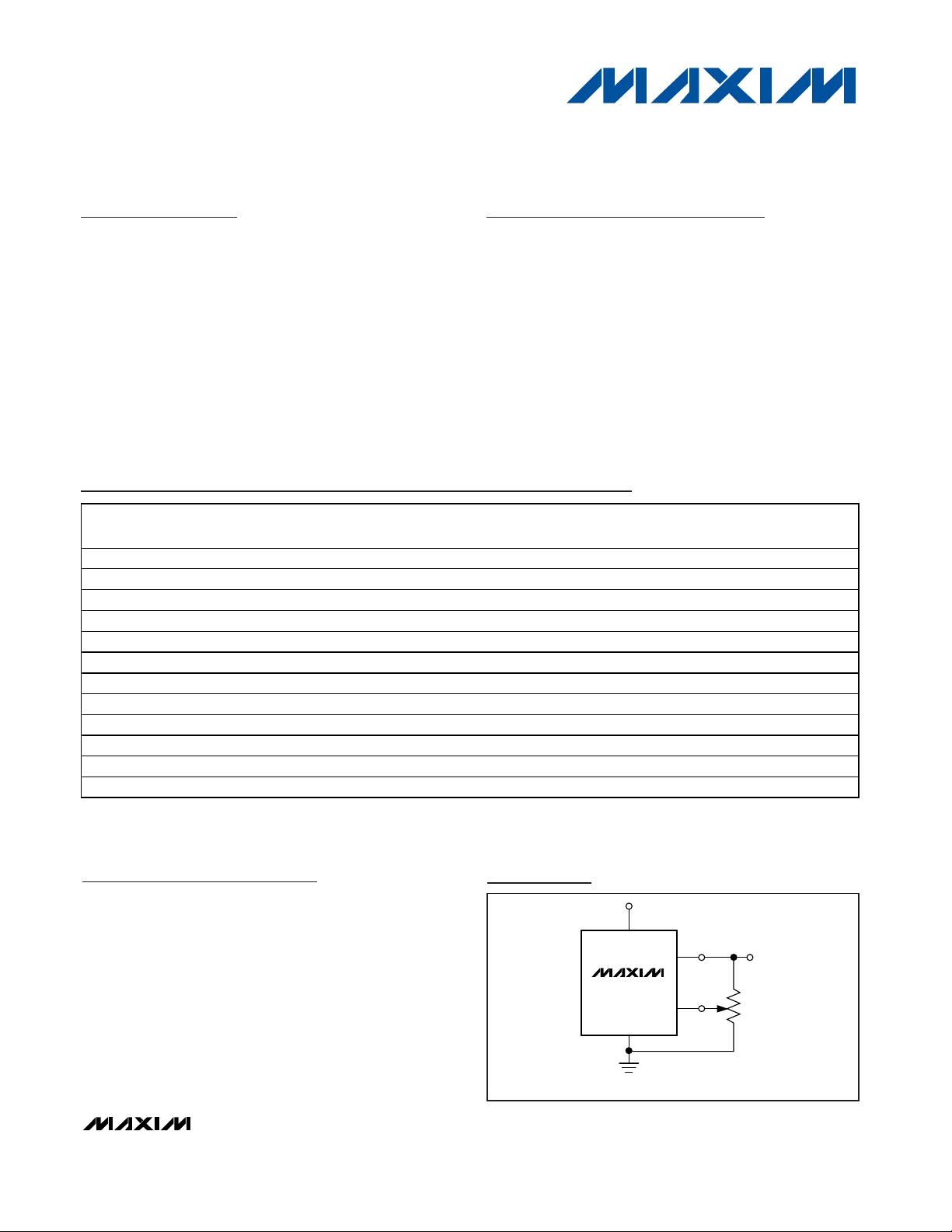
Ordering Information
REF01
REF02
OUTPUT
R
P
10kΩ
6
5
TRIM
V
O
V
IN
+15V
4
GND
REFERENCE WITH TRIMMED OUTPUT.
2
Typical Operating Circuit
19-0887; Rev 7; 4/07
For pricing, delivery, and ordering information, please contact Maxim/Dallas Direct! at
1-888-629-4642, or visit Maxim’s website at www.maxim-ic.com.
Applications
Analog-to-Digitial Converters
Digitial-to-Analog Converters
Digital Voltmeters
Voltage Regulators
Threshold Detectors
+Denotes a lead-free package.
Ordering Information continued at end of data sheet.
Page 2
REF01/REF02
+5V, +10V Precision
Voltage References
2 _______________________________________________________________________________________
ABSOLUTE MAXIMUM RATINGS–REF01
ELECTRICAL CHARACTERISTICS—REF01E/REF01H
(VIN= +15V, TA= +25°C, unless otherwise noted.)
ELECTRICAL CHARACTERISTICS
—REF01E/REF01H
(VIN= +15V, 0°C ≤ TA≤ +70°C for REF01E and REF01H, IL= 0mA, unless otherwise noted.)
Stresses beyond those listed under “Absolute Maximum Ratings” may cause permanent damage to the device. These are stress ratings only, and functional
operation of the device at these or any other conditions beyond those indicated in the operational sections of the specifications is not implied. Exposure to
absolute maximum rating conditions for extended periods may affect device reliability.
Input Voltage
REF01, E, H .........................................................................40V
REF01C ...............................................................................30V
Continuous Power Dissipation
Plastic Dip (P) (derate at 5.6mW/°C above +36°C) .....500mW
Small Outline (S) (derate at 5.0mW/°C above +55°C) ..300mW
Output Short-Circuit Duration
(to ground or V
IN
) .......................................................Indefinite
Storage Temperature Range .............................-65°C to +150°C
Operating Temperature Range
REF01E, REF01H, REF01C
(except REF01CESA)...........................................0°C to +70°C
REF01CESA......................................................-40°C to +85°C
Lead Temperature (soldering, 60s) .................................+300°C
REF01E REF01H
PARAMETER
SYMBOL
CONDITIONS
MIN TYP MAX MIN
UNITS
Output Voltage V
O
IL = 0 9.97
V
Output Adjustment Range
∆V
trim
RP = 10kΩ ±3.0 ±6.0
%
Output Voltage Noise e
nP-P
0.1Hz to 10Hz (Note 1) 20 30 20 30 µV
P-P
Line Regulation
%/V
Load Regulation IL = 0 to 10mA (Note 2)
%/mA
Turn-On Settling Time t
ON
To ±0.1% of final value 400 400 µs
Quiescent Supply Current
I
SY
No load 1.0 1.4 1.0 1.4 mA
Load Current I
L
To specified output
voltage tolerance
10 21 10 21 mA
Sink Current I
S
To specified output
voltage tolerance
0.3 0.5 0.3 0.5 mA
Short-Circuit Current I
SC
VO = 0V 30 30 mA
TYP MAX
10.00 10.03 9.95 10.00 10.05
±3.0 ±6.0
VIN = 13V to 33V (Note 2) 0.006 0.010 0.006 0.010
0.005 0.008 0.006 0.010
PARAMETER SYMBOL CONDITIONS
Output Voltage Change with
Temperature
Output Voltage Temperature
Coefficient
Change in VO Temperature
Coefficient with Output
Adjustment
Line Regulation
(VIN = 13V to 33V)
Load Regulation
(IL = 0 to 8mA)
∆V
OT
TCV
O
REF01E REF01H
MIN TYP MAX MIN TYP MAX
0°C ≤ T
≤ +70°C
A
(Note 3)
(Note 4) 3 8.5 10.0 25.0 ppm/°C
RP = 10kΩ 0.7 0.7 ppm/%
0°C ≤ TA ≤ +70°C
(Note 2)
0°C ≤ TA ≤ +70°C
(Note 2)
0.02 0.06 0.07 0.17 %
0.007 0.012 0.007 0.012 %/V
0.006 0.010 0.007 0.012 %/mA
UNITS
Page 3
Note 1: Guaranteed by design.
Note 2: Line and load regulation specifications include the effect of self heating. 100% production tested at T
A
= +25°C and guaranteed
by design for T
A
= T
MIN
to T
MAX
, as specified.
Note 3: ∆V
OT
is defined as the absolute difference between the maximum output voltage and the minimum output voltage over the
specified temperature range expressed as a percentage of 10V. Guaranteed by design.
Note 4: TCV
O
is defined as ∆VOTdivided by the temperature range. Guaranteed by design.
∆VOT=
⎡
⎣
⎢
⎤
⎦
⎥
×
V-V
10V
100
MAX MIN
REF01/REF02
+5V, +10V Precision
Voltage References
_______________________________________________________________________________________ 3
ELECTRICAL CHARACTERISTICS—REF01C
(VIN= +15V, TA= +25°C, IL= 0mA, unless otherwise noted.)
REF01C
PARAMETER
SYMBOL
CONDITIONS
MIN TYP MAX
UNITS
Output Voltage V
O
IL = 0mA 9.90 10.00 10.10 V
Output Adjustment Range ∆V
trim
RP = 10kΩ ±2.7 ±6.0 %
Output Voltage Noise e
nP-P
0.1Hz to 10Hz (Note 1) 25 35 µV
P-P
Line Regulation VIN = 13V to 30V (Note 2) 0.009 0.015 %/V
IL = 0 to 8mA 0.006 0.015
Load Regulation (Note 2)
IL = 0 to 4mA 0.006 0.015
%/mA
Turn-On Settling Time t
ON
To ±0.1% of final value 400 µs
Quiescent Supply Current I
SY
No load 1.0 1.6 mA
Load Current I
L
To specified output voltage tolerance 8 21 mA
Sink Current I
S
To specified output voltage tolerance 0.2 0.5 mA
Short-Circuit Current I
SC
VO = 0V 30 mA
ELECTRICAL CHARACTERISTICS—REF01C
(VIN= +15V, TA= T
MIN
to T
MAX
, unless otherwise noted.)
REF01C
PARAMETER
SYMBOL
CONDITIONS
MIN TYP MAX
UNITS
Output Voltage Change with
Temperature
∆V
OT
(Note 3) 0.14 0.45 %
Output Voltage Temperature
Coefficient
TCV
O
(Note 4) 20 65 ppm/°C
Change in VO Temperature
Coefficient with Output Adjustment
RP = 10kΩ 0.7 ppm/%
Line Regulation VIN = 13V to 30V (Note 2) 0.011 0.018 %/V
Load Regulation IL = 0 to 5mA (Note 2) 0.008 0.018 %/mA
Output Adjustment
The REF01 trim terminal can be used to adjust the voltage over a 10V ±600mV range. This feature allows the
system designer to trim system errors by setting the reference to a voltage other than 10V, including 10.240V for
binary applications (see the Typical Operating Circuit).
Adjustment of the output does not significantly affect the
temperature performance of the device. The temperature coefficient change is approximately 0.7ppm/°C for
100mV of output adjustment.
Page 4

REF01/REF02
+5V, +10V Precision
Voltage References
4 _______________________________________________________________________________________
ABSOLUTE MAXIMUM RATINGS–REF02
Input Voltage
REF02, E, H .........................................................................40V
REF02C ...............................................................................30V
Continuous Power Dissipation
Plastic Dip (P) (derate at 5.6mW/°C above +36°C) .....500mW
Small Outline (S) (derate at 5.0mW/°C above +55°C) ..300mW
Storage Temperature Range .............................-65°C to +150°C
Operating Temperature Range
REF02E, REF02H .................................................0°C to +70°C
REF02C (except REF02CESA) ............................0°C to +70°C
REF02CESA......................................................-40°C to +85°C
Output Short-Circuit Duration
(to ground or V
IN
) .......................................................Indefinite
Lead Temperature (soldering, 60s) .................................+300°C
ELECTRICAL CHARACTERISTICS—REF02E/REF02H
(VIN= +15V, 0°C ≤ TA≤ +70°C for REF02E and REF02H, IL= 0mA, unless otherwise noted.)
ELECTRICAL CHARACTERISTICS—REF02E/REF02H
(VIN= +15V, TA= +25°C, unless otherwise noted.)
REF02E REF02H
PARAMETER
SYMBOL
CONDITIONS
UNITS
Output Voltage V
O
IL = 0
V
Output Adjustment Range
RP = 10kΩ ±3 ±6 ±3 ±6 %
Output Voltage Noise e
nP-P
0.1Hz to 10Hz (Note 5) 10 15 10 15 µV
P-P
Line Regulation VIN = 8V to 33V (Note 6)
%/V
Load Regulation IL = 0 to 10mA (Note 6)
%/mA
Turn-On Settling Time t
ON
To ±0.1% of final value
µs
Quiescent Supply Current I
SY
No load 1.0 1.4 1.0 1.4 mA
Load Current I
L
10 21 10 21 mA
Sink Current I
S
0.3 0.5 0.3 0.5 mA
Short-Circuit Current I
SC
VO = 0V 30 30 mA
T em p e r a t ur e V ol ta g e Ou tp u t
V
T
(Note 7)
mV
Stresses beyond those listed under “Absolute Maximum Ratings” may cause permanent damage to the device. These are stress ratings only, and functional
operation of the device at these or any other conditions beyond those indicated in the operational sections of the specifications is not implied. Exposure to
absolute maximum rating conditions for extended periods may affect device reliability.
∆V
trim
MIN TYP MAX MIN TYP MAX
4.985 5.000 5.015 4.975 5.000 5.025
0.006 0.010 0.006 0.010
0.005 0.010 0.006 0.010
230 230
To specified output voltage tolerance
To specified output voltage tolerance
PARAMETER SYMBOL CONDITIONS
Output Voltage Change with
Temperature
Output Voltage Temperature
Coefficient
Change in VO Temperature
Coefficient with Output
Adjustment
Line Regulation
(V
= 8V to 33V)
I N
Load Regulation
(IL = 0 to 8mA)
∆V
TCV
0°C ≤ TA ≤ +70°C
OT
(Note 8)
(Note 9) 3 8.5 10 25 ppm/°C
O
RP = 10kΩ 0.7 0.7 ppm/%
0°C ≤ TA ≤ +70°C
(Note 6)
0°C ≤ TA ≤ +70°C
(Note 6)
630 630
REF02E REF02H
MIN TYP MAX MIN TYP MAX
0.02 0.06 0.07 0.17 %
0.007 0.012 0.007 0.012 %/V
0.006 0.010 0.007 0.012 %/mA
UNITS
Page 5

REF01/REF02
+5V, +10V Precision
Voltage References
_______________________________________________________________________________________ 5
ELECTRICAL CHARACTERISTICS—REF02E/REF02H (continued)
(VIN= +15V, 0°C ≤ TA≤ +70°C for REF02E and REF02H, IL= 0mA, unless otherwise noted.)
REF02E REF02H
PARAMETER
SYMBOL
CONDITIONS
MIN TYP
UNITS
Temperature Voltage Output
Temperature Coefficient
TCV
T
(Note 7) 2.1 2.1 mV/°C
ELECTRICAL CHARACTERISTICS—REF02C
(VIN= +15V, TA= +25°C, unless otherwise noted.)
REF02C
PARAMETER
CONDITIONS
UNITS
Output Voltage V
O
IL = 0mA
V
Output Adjustment Range ∆V
trim
RP = 10kΩ
%
Output Voltage Noise e
nP-P
0.1Hz to 10Hz (Note 5) 12 18 µV
P-P
Line Regulation VIN = 8V to 30V (Note 6)
%/V
IL = 0 to 8mA
Load Regulation (Note 6)
IL = 0 to 4mA
%/mA
Turn-On Settling Time t
ON
To ±0.1% of final value 230 µs
Quiescent Supply Current I
SY
No load 1.0 1.6 mA
Load Current I
L
To specified output voltage tolerance 8 21 mA
Sink Current I
S
To specified output voltage tolerance 0.2 0.5 mA
Short-Circuit Current I
SC
VO = 0V 30 mA
Temperature Voltage Output V
T
(Note 7) 630 mV
ELECTRICAL CHARACTERISTICS—REF02C
(VIN= +15V, TA= T
MIN
to T
MAX
, IL= 0mA, unless otherwise noted.)
REF02C
PARAMETER
SYMBOL
CONDITIONS
UNITS
Output Voltage Change with
Temperature
∆V
OT
(Note 8)
%
Output Voltage Temperature
Coefficient
TCV
O
(Note 9) 20 65 ppm/°C
Change in VO Temperature
Coefficient with Output
Adjustment
RP = 10kΩ 0.7 ppm/%
Line Regulation VIN = 8V to 30V (Note 6)
%/V
Load Regulation IL = 0 to 5mA (Note 6)
%/mA
Temperature Voltage Output
Temperature Coefficient
TCV
T
(Note 7) 2.1 mV/°C
MAX MIN TYP MAX
SYMBOL
MIN TYP MAX
4.950 5.000 5.050
±2.7 ±6.0
0.009 0.015
0.006 0.015
MIN TYP MAX
0.14 0.45
0.011 0.018
0.008 0.018
Page 6
REF01/REF02
+5V, +10V Precision
Voltage References
6 _______________________________________________________________________________________
Output Adjustment
The REF02 trim terminal can be used to adjust the output voltage over a 5V ±300mV range. This feature
allows the system designer to trim system errors by setting the reference to a voltage other than 5V (refer to
the Typical Operating Circuit).
Adjustment of the output does not significantly affect
the temperature performance of the device. Typically,
the temperature coefficient change is 0.7ppm/°C for
100mV of output adjustment.
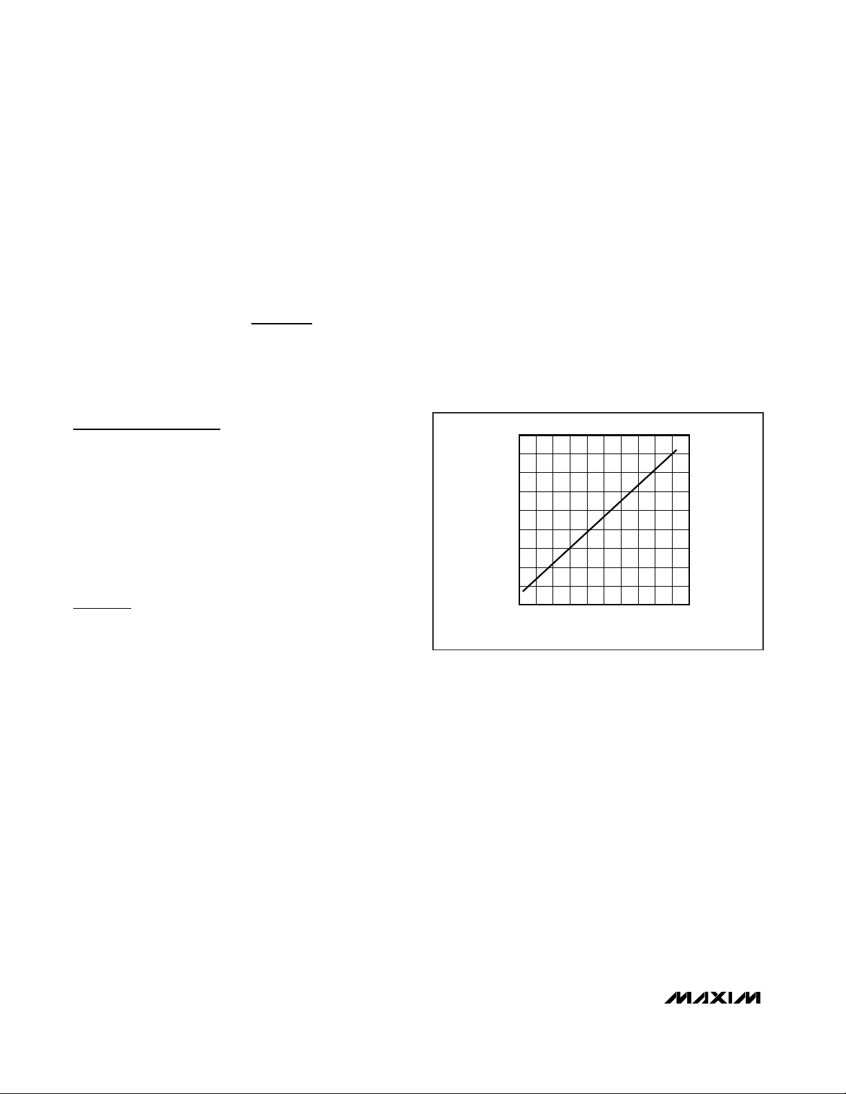
Temperature Voltage Output
The REF02 provides a temperature-dependent output
voltage on the TEMP pin. This voltage is proportional to
the absolute temperature, and has a scale factor of
approximately 2.1mV/°C (Figure 1).
Output Voltage = 2.1(T + 273)mV
where T = Temperature in °C.
430
530
480
630
580
680
730
830
780
880
-60 -40 -20 0 20 40 60 80 100 120 140
TEMPERATURE (°C)
TEMP VOLTAGE OUTPUT (mV)
Figure 1. REF02 Temperature/Voltage Output vs. Temperature
ELECTRICAL CHARACTERISTICS–REF02 (continued)
(VIN= +15V, TA= T
MIN
to T
MAX
, IL= 0mA, unless otherwise noted.)
Note 5: Guaranteed by design.
Note 6: Line and load regulation specifications include the effect of self heating. 100% production tested at T
A
= +25°C and guaranteed
by design for T
A
= T
MIN
to T
MAX
, as specified.
Note 7: Limit current in or out of pin 3 to 50nA and capacitance on pin 3 to 30pF.
Note 8: ∆V
OT
is defined as the absolute difference between the maximum output voltage and the minimum output voltage over the
specified temperature range expressed as a percentage of 5V. Guaranteed by design.
Note 9: TCV
O
is defined as ∆VOTdivided by the temperature range. Guaranteed by design.
∆VOT=
⎡
⎣
⎢
⎤
⎦
⎥
×
V-V
5V
100
MAX MIN
Page 7

REF01/REF02
+5V, +10V Precision
Voltage References
_______________________________________________________________________________________ 7
Typical Operating Characteristics
(TA = +25°C, unless otherwise noted.)
6
26
16
46
36
66
56
76
10 1k100 10k 100k 1M
LINE REGULATION
vs. FREQUENCY
REF01/02 TOC01
FREQUENCY (Hz)
LINE REGULATION (dB)
VIN = 15V
T
A
= +25°C
10
100
1000
10,000
10 1k100 10k 100k 1M
REF01 OUTPUT WIDEBAND
NOISE vs. BANDWIDTH
(0.1Hz TO FREQUENCY INDICATED)
REF01/02 TOC02
FREQUENCY (Hz)
OUTPUT NOISE (µV
P-P
)
VIN = 15V
T
A
= +25°C
10
100
1000
10,000
10 1k100 10k 100k 1M
REF02 OUTPUT WIDEBAND
NOISE vs. BANDWIDTH
(0.1Hz TO FREQUENCY INDICATED)
REF01/02 TOC03
FREQUENCY (Hz)
OUTPUT NOISE (µV
P-P
)
VIN = 15V
T
A
= +25°C
0
15
10
5
25
20
30
35
10 15 20 25 30
MAXIMUM LOAD CURRENT
vs. INPUT VOLTAGE
REF01/02 TOC04
INPUT VOLTAGE (V)
MAXIMUM LOAD CURRENT (mA)
500mW MAXIMUM
DISSIPATION
SHORT-CIRCUIT
PROTECTION
TA = +25°C
0.6
0.8
0.7
1.0
0.9
1.3
1.2
1.1
1.4
-60 200-20-40 60 8040 100 120 140
NORMALIZED LOAD
REGULATION (∆I
L
= 10mA)
vs. TEMPERATURE
REF01/02 TOC05
TEMPERATURE (°C)
LOAD REG (T)/LOAD REG (+25°C)
VIN = 15V
0.6
0.8
0.7
1.0
0.9
1.3
1.2
1.1
1.4
-60 200-20-40 60 8040 100 120 140
NORMALIZED LINE REGULATION
vs. TEMPERATURE
REF01/02 TOC06
TEMPERATURE (°C)
LOAD REG (T)/LOAD REG (+25°C)
0
5
15
10
25
20
30
-60 200-20-40 60 8040 100 120 140
MAXIMUM LOAD CURRENT
vs. TEMPERATURE
REF01/02 TOC07
TEMPERATURE (°C)
MAXIMUM LOAD CURRENT (mA)
VIN = 15V
0.7
0.8
1.0
0.9
1.2
1.1
1.3
-60 200-20-40 60 8040 100 120 140
QUIESCENT CURRENT
vs. TEMPERATURE
REF01/02 TOC08
TEMPERATURE (°C)
QUIESCENT CURRENT (mA)
VIN = 15V
0
0.010
0.005
0.015
0.030
0.025
0.020
0.035
-10 3020100506040
OUTPUT CHANGE DUE TO
THERMAL SHOCK
REF01/02 TOC09
TIME (s)
PERCENT CHANGE OUTPUT VOLTAGE (%)
VIN = 15V
TA =
+25°C
TA =
+75°C
DEVICE IMMERSED
IN +75°C OIL BATH
Page 8

REF01/REF02
+5V, +10V Precision
Voltage References
8 _______________________________________________________________________________________
Typical Applications
100kΩ
6
5
9V
9V
-
+
TRIM
10.000V
V
O
V
IN
1.1mA
4
GND
2
REF01
Figure 2. Precision Calibration Standard Figure 3. ±10V Reference
R
6
53
TRIM
V
O
V
IN
+15V
4
I
OUT
GND
2
I
OUT
= + 1mA
5.0V
R
REF02
Figure 4. Current Source Figure 5. Precision Temperature Transducer with
Remote Sensor
+15V
2
V
IN
6
V
O
+10V
2
V
IN
REF02
TRIM
TEMP
GND
4
*UP TO 10 FEET OF SHIELDED
4-CONDUCTOR CABLE.
REF01
GND
V
O
4
6
5
TRIM
1.5kΩ
±5%
5
5kΩ
10kΩ
10kΩ
+15V
+15V
5.11kΩ
7
4
-15V
-10V
6
V
OUT
(10mV/°C)
OP-07
-15V
9.09kΩ
V
REF
50kΩ
1.5kΩ
*
2
OP-07
3
200kΩ
Page 9

REF01/REF02
+5V, +10V Precision
Voltage References
Maxim cannot assume responsibility for use of any circuitry other than circuitry entirely embodied in a Maxim product. No circuit patent licenses are
implied. Maxim reserves the right to change the circuitry and specifications without notice at any time.
Maxim Integrated Products, 120 San Gabriel Drive, Sunnyvale, CA 94086 408-737-7600 _____________________ 9
© 2007 Maxim Integrated Products is a registered trademark of Maxim Integrated Products, Inc.
TOP VIEW
V
OUT
TRIMGND
1
2
87N.C.
N.C.V
IN
N.C./TEMP*
N.C.
DIP
3
4
6
5
REF01/
REF02
V
OUT
TRIMGDN
1
2
87N.C.
N.C.V
IN
N.C./TEMP*
N.C.
SO
3
4
6
5
REF01/
REF02
Pin Configurations
*NOTE: PIN 3 IS N.C. (NO CONNECTION) ON REF01, TEMP OUTPUT ON REF02.
PART TEMP RANGE
MAX TEMPCO
(ppm/°C)
INITIAL ERROR
(mV)
PIN-PACKAGE
PKG
CODE
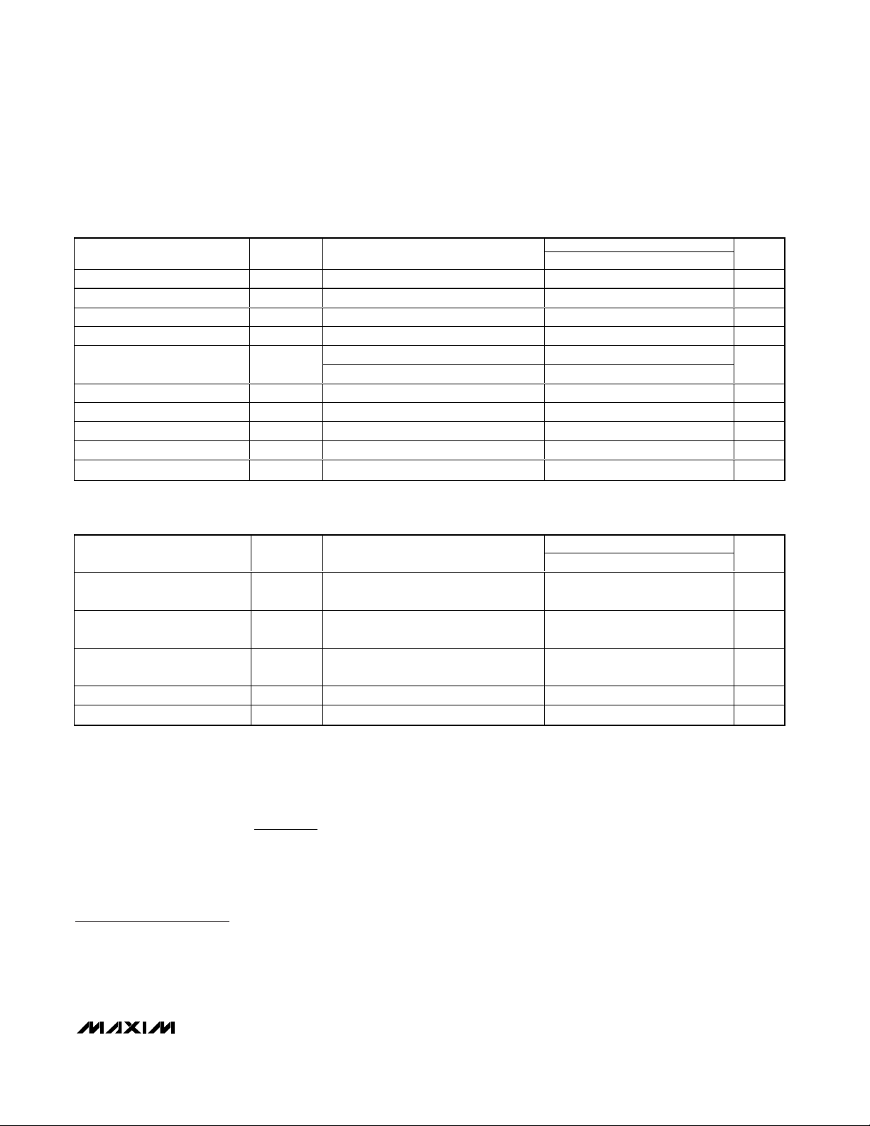
REF02EP 0°C to +70°C 8.5 ±15 8 Plastic DIP P8-2
REF02EP+ 0°C to +70°C 8.5 ±15 8 Plastic DIP P8-2
REF02HP 0°C to +70°C 25 ±25 8 Plastic DIP P8-2
REF02HP+ 0°C to +70°C 25 ±25 8 Plastic DIP P8-2
REF02HSA 0°C to +70°C 25 ±25 8 SO S8-2
REF02HSA+ 0°C to +70°C 25 ±25 8 SO S8-2
REF02CP 0°C to +70°C 65 ±50 8 Plastic DIP P8-2
REF02CP+ 0°C to +70°C 65 ±50 8 Plastic DIP P8-2
REF02CSA 0°C to +70°C 65 ±50 8 SO S8-2
REF02CSA+ 0°C to +70°C 65 ±50 8 SO S8-2
REF02CESA -40°C to +85°C 65 ±50 8 SO S8-2
REF02CESA+ -40°C to +85°C 65 ±50 8 SO S8-2
Ordering Information (continued)
Package Information
For the latest package outline information, go to
www.maxim-ic.com/packages
.
Revision History
Pages changed at Rev 7: 1, 9
+Denotes a lead-free package.
 Loading...