

For free samples & the latest literature: http://www.maxim-ic.com, or phone 1-800-998-8800.
For small orders, phone 1-800-835-8769.
General Description
The MAX6326/MAX6327/MAX6328/MAX6346/MAX6347/
MAX6348 microprocessor (µP) supervisory circuits monitor the power supplies in µP and digital systems. These
devices provide excellent circuit reliability and low cost
by eliminating external components and adjustments
when used with 2.5V, 3V, 3.3V, and 5V powered circuits.
These circuits perform a single function: they assert a
reset signal whenever the VCCsupply voltage declines
below a preset threshold, keeping it asserted for at least
100ms after VCChas risen above the reset threshold.
The only difference between the devices is their output.
The MAX6326/MAX6346 (push-pull) and MAX6328/
MAX6348 (open-drain) have an active-low reset output.
The MAX6327/MAX6347 have an active-high push-pull
reset output. All of these parts are guaranteed to be in
the correct state for VCCdown to 1V. The reset comparator is designed to ignore fast transients on VCC. Reset
thresholds are factory-trimmable between 2.2V and
4.63V, in approximately 100mV increments. Twenty-one
standard versions are available. Contact the factory for
availability of nonstandard versions.
Ultra-low supply currents (1µA max for the MAX6326/
MAX6327/MAX6328) make these parts ideal for use in
portable equipment. All six devices are available in
space-saving SOT23 and SC70 packages.
Applications
Computers Intelligent Instruments
Controllers Automotive
Critical µP and µC Portable/Battery-Powered
Power Monitoring Equipment
Features
♦ Ultra-Low 1µA (max) Supply Current
(MAX6326/MAX6327/MAX6328)
♦ Precision Monitoring of 2.5V, 3V, 3.3V, and 5V
Power-Supply Voltages
♦ Reset Thresholds Available from 2.2V to 4.63V
♦ Fully Specified Over Temperature
♦ 100ms (min) Power-On Reset Pulse Width
♦ Low Cost
♦ Available in Three Versions: Push-Pull RESET,
Push-Pull RESET, and Open-Drain RESET
♦ Power-Supply Transient Immunity
♦ No External Components
♦ 3-Pin SC70/SOT23 Packages
♦ Pin Compatible with MAX803/MAX809/MAX810
MAX6326/MAX6327/MAX6328/MAX6346/MAX6347/MAX6348
3-Pin, Ultra-Low-Power SC70/SOT
µP Reset Circuits
________________________________________________________________ Maxim Integrated Products 1
Pin Configuration
19-1294; Rev 3; 1/00
†The MAX6326/MAX6327/MAX6328/MAX6346/MAX6347/
MAX6348 are available in factory-set V
CC
reset thresholds from
2.2V to 4.63V, in approximately 0.1V increments. Choose the
desired reset-threshold suffix from Table 1 and insert it in the
blank spaces following “R.” There are 21 standard versions with
a required order increment of 2500 pieces. Sample stock is generally held on the standard versions only (see the Selector
Guide). Required order increment is 10,000 pieces for nonstandard versions (Table 2). Contact factory for availability. All
devices available in tape-and-reel only.
Ordering Information
3 SC70-3
3 SC70-3
3 SC70-3-40°C to +85°C
-40°C to +85°C
-40°C to +85°C
MAX6348XR_ _-T
MAX6347XR_ _-T
MAX6346XR_ _-T
3 SC70-3
3 SC70-3
3 SC70-3
PIN-PACKAGETEMP. RANGE
-40°C to +85°C
-40°C to +85°C
-40°C to +85°C
MAX6328XR_ _-T
MAX6327XR_ _-T
MAX6326XR_ _-T
PART
†
3 SOT23-3-40°C to +85°CMAX6326UR_ _-T
3 SOT23-3-40°C to +85°CMAX6327UR_ _-T
3 SOT23-3-40°C to +85°CMAX6328UR_ _-T
3 SOT23-3-40°C to +85°CMAX6346UR_ _-T
3 SOT23-3-40°C to +85°CMAX6347UR_ _-T
3 SOT23-3-40°C to +85°CMAX6348UR_ _-T
Selector Guide appears at end of data sheet.
TOP VIEW
GND
1
MAX6326
MAX6327
(RESET) RESET
MAX6328
MAX6346
MAX6347
MAX6348
2
3 V
CC
SOT23-3/SC70-3
( ) ARE FOR THE MAX6327/MAX6347.
MAX6326/MAX6327/MAX6328/MAX6346/MAX6347/MAX6348
3-Pin, Ultra-Low-Power SC70/SOT
µP Reset Circuits
2 _______________________________________________________________________________________
ABSOLUTE MAXIMUM RATINGS
ELECTRICAL CHARACTERISTICS
(VCC= full range, TA= -40°C to +85°C, unless otherwise noted. Typical values are at TA= +25°C and VCC= 3V.) (Note 1)
Stresses beyond those listed under “Absolute Maximum Ratings” may cause permanent damage to the device. These are stress ratings only, and functional
operation of the device at these or any other conditions beyond those indicated in the operational sections of the specifications is not implied. Exposure to
absolute maximum rating conditions for extended periods may affect device reliability.
Terminal Voltage (with respect to GND)
V
CC
...........................................................................-0.3V to +6V
RESET, RESET (push-pull) .........................-0.3V to (V
CC
+ 0.3V)
RESET (open drain)..................................................-0.3V to +6V
Input Current (V
CC
).............................................................20mA
Output Current (RESET, RESET).........................................20mA
Rate of Rise (V
CC
) ...........................................................100V/µs
Continuous Power Dissipation (T
A
= +70°C)
3-Pin SC70 (derate 2.7mW/°C above +70°C)...............174mW
3-Pin SOT23 (derate 4mW/°C above +70°C)................320mW
Operating Temperature Range ...........................-40°C to +85°C
Storage Temperature Range .............................-65°C to +150°C
Lead Temperature (soldering, 10s) .................................+300°C
Note 1: Overtemperature limits are guaranteed by design and not production tested.
RESET Output Voltage
(MAX6327/MAX6347)
V
OL
0.4I
SINK
= 3.2mA, VCC= V
TH(MAX)
, VTH≥ 4.5V
0.4
I
SINK
= 3.2mA, VCC≥ 4.5V, reset not asserted,
VTH≤ 4.38V
V
V
OH
I
SOURCE
= 50µA, VCC≥ 1.2V, reset asserted
0.3
I
SINK
= 1.2mA, VCC≥ 3.2V, reset not asserted,
MAX6327 only
0.8 · V
CC
0.8 · V
CC
I
SOURCE
= 500µA, VCC≥ 2.1V, reset asserted
1.0 1.75
µA
0.5 1.0
Supply Current I
CC
VCC= 5.5V, no load
Reset Threshold
VTH-
V
TH
VTH+
1.5% 1.5%
VV
TH
VTH-
V
TH
VTH+
2.5% 2.5%
Table 1
TA= +25°C
TA= -40°C to +85°C
1.2 5.5
1.0 5.5
0.8 · V
CC
0.8 · V
CC
0.8 · V
CC
Open-Drain RESET Output
Leakage Current
µA0.1
RESET Threshold
Hysteresis
mV
9.5MAX6346/MAX6347/MAX6348
6.3MAX6326/MAX6327/MAX6328
VCCto Reset Delay 20 µsVCC= VTHto (VTH- 100mV)
PARAMETER SYMBOL MIN TYP MAX UNITS
ms100 185 280
VCCRange V
Reset Threshold Tempco ∆VTH/°C 40 ppm/°C
CONDITIONS
TA= 0°C to +70°C
TA= -40°C to +85°C
V
Reset Active Timeout Period
I
SOURCE
= 800µA, VCC= V
TH(MAX)
, VTH≥ 4.5V
RESET Output Voltage
(MAX6326/MAX6346)
I
SOURCE
= 800µA, VCC= 4.5V, VTH≤ 4.38V
V
OH
I
SOURCE
= 500µA, VCC= 3.2V, MAX6326 only
MAX632_ only, VCC= 3.0V for VTH≤ 2.93V,
VCC= 3.2V for VTH> 2.93V, no load
V
0.3I
SINK
= 1.6mA, VCC> 2.1V, reset asserted
RESET Output Voltage
(MAX6326/MAX6328/
MAX6346/MAX6348)
V
OL
0.4I
SINK
= 100µA, VCC≥ 1.2V, reset asserted
PIN
MAX6326/MAX6327/MAX6328/MAX6346/MAX6347/MAX6348
3-Pin, Ultra-Low-Power SC70/SOT
µP Reset Circuits
_______________________________________________________________________________________ 3
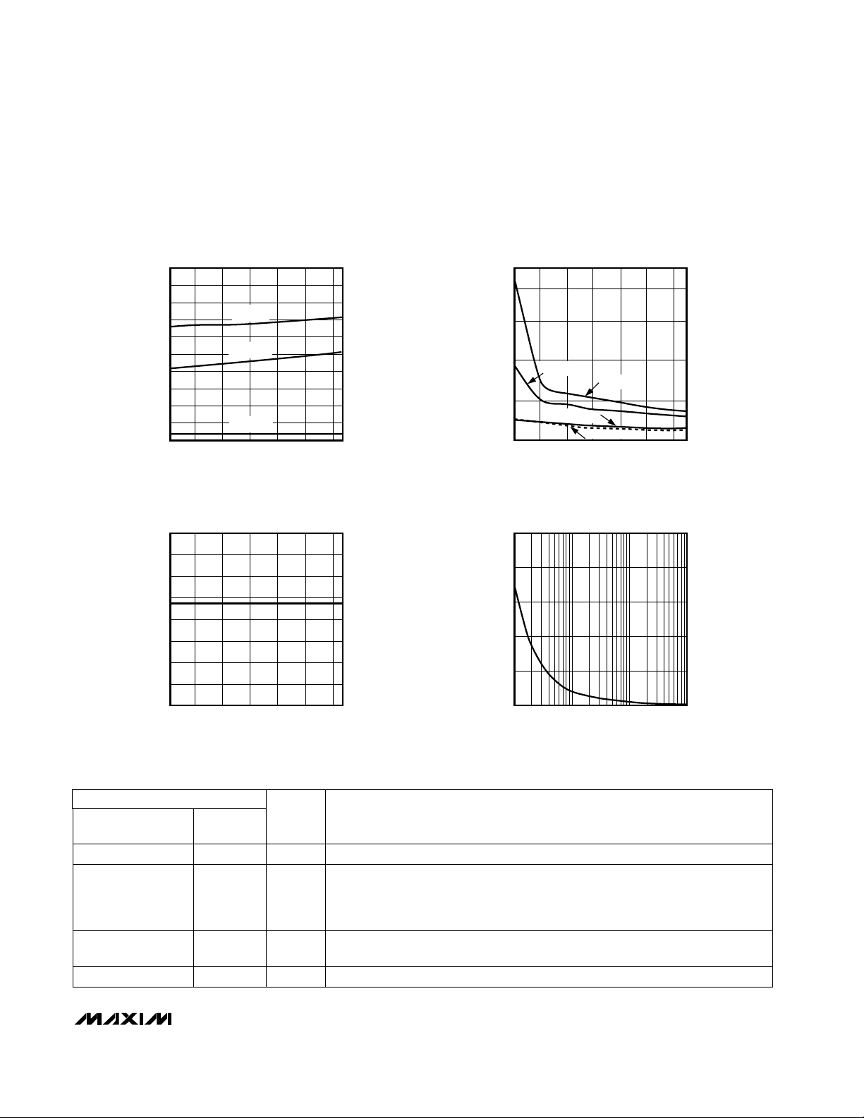
__________________________________________Typical Operating Characteristics
(TA = +25°C, unless otherwise noted.)
______________________________________________________________Pin Description
FUNCTION
1 1 Ground
2 —
Active-Low Reset Output. RESET remains low while VCCis below the reset
threshold and for at least 100ms after V
CC
rises above the reset threshold.
RESET is open-drain on the MAX6328/MAX6348 and push-pull on the
MAX6326/MAX6346.
— 2
Active-High Reset Output. RESET remains high while VCCis below the reset
threshold and for at least 100ms after V
CC
rises above the reset threshold.
3 3 Supply Voltage
NAME
GND
RESET
RESET
V
CC
MAX6327
MAX6347
MAX6326/MAX6346
MAX6328/MAX6348
PIN
SUPPLY CURRENT vs. TEMPERATURE
1.0
0.9
0.8
0.7
0.6
0.5
0.4
0.3
SUPPLY CURRENT (µA)
0.2
0.1
0
-40 0-20 20 40 60 80
VCC = 5V
VCC = 3.3V
VCC = 1.2V
TEMPERATURE (°C)
POWER-UP RESET TIMEOUT
vs. TEMPERATURE
210
200
190
180
170
160
150
POWER-UP RESET TIMEOUT (ms)
140
130
-40 0-20 20 40 60 80
TEMPERATURE (°C)
MAX6326-01
MAX6326-03
200
150
100
RESET DELAY (µs)
50
500
400
300
200
100
MAXIMUM TRANSIENT DURATION (µs)
POWER-DOWN RESET DELAY
vs. TEMPERATURE
VOD = 20mV
VOD = 100mV
0
-40 0-20 20 40 60 80
VOD = 10mV
VOD = 200mV
TEMPERATURE (°C)
MAXIMUM TRANSIENT DURATION
vs. RESET THRESHOLD OVERDRIVE (SC70)
0
1 100 1000
10
RESET THRESHOLD OVERDRIVE,
V
- V
(mV)
TH
CC
MAX6326-02
MAX6326-04

MAX6326/MAX6327/MAX6328/MAX6346/MAX6347/MAX6348
3-Pin, Ultra-Low-Power SC70/SOT
µP Reset Circuits
4 _______________________________________________________________________________________
____________ Applications Information
Interfacing to µPs with
Bidirectional Reset Pins
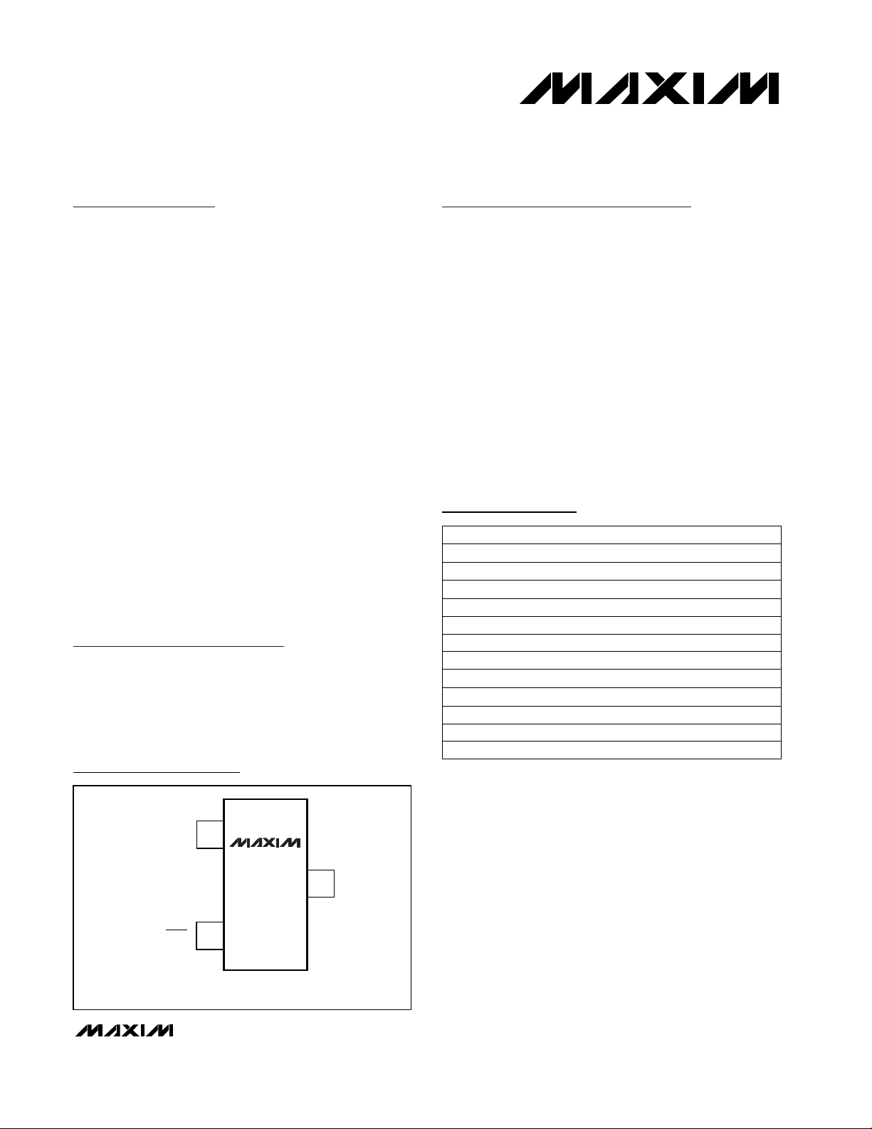
Since the RESET output on the MAX6328/MAX6348 is
open drain, these devices interface easily with microprocessors (µPs) that have bidirectional reset pins,
such as the Motorola 68HC11. Connecting the µP
supervisor’s RESET output directly to the microcontroller’s (µC’s) RESET pin with a single pull-up resistor
allows either device to assert reset (Figure 1).
Negative-Going VCCTransients
In addition to issuing a reset to the µP during power-up,
power-down, and brownout conditions, these devices
are relatively immune to short-duration, negative-going
VCCtransients (glitches).
The Typical Operating Characteristics show the Maxi-
mum Transient Duration vs. Reset Threshold Overdrive
graph, for which reset pulses are not generated. The
graph shows the maximum pulse width that a negativegoing VCCtransient may typically have when issuing a
reset signal. As the amplitude of the transient increases, the maximum allowable pulse width decreases.
Figure 1. Interfacing to µPs with Bidirectional Reset Pins
Table 1. Factory-Trimmed Reset Thresholds
‡
‡
Factory-trimmed reset thresholds are available in approximately 100mV increments with a 1.5% room-temperature variance.
3.800 3.8953.857 3.705
3.700
3.74338
3.7923.755 3.6073.64437
3.600 3.6903.654 3.510
3.500
3.54636
3.5873.552 3.4123.44735
3.400 3.4853.451 3.315
3.300
3.34934
3.3833.350 3.2173.25033
3.080 3.1503.126 3.003
3.000
3.03431
3.0753.045 2.9252.95530
2.930 3.0002.974 2.857
2.800
2.88629
2.8702.842 2.7302.75828
2.700 2.7682.741 2.633
2.630
2.66027
2.6962.669 2.5642.59126
2.500 2.5622.537 2.437
2.400
2.46225
2.4602.436 2.3402.36424
2.320 2.3752.355 2.2622.28523
MIN
TYP
MAXMAX MIN
TA= -40°C to +85°CTA= +25°C
2.250
RESET THRESHOLD VOLTAGE, VTH(V)
2.1452.2332.2002.167
SUFFIX
MAX634_ _R
MAX634_ _R
MAX634_ _R
MAX634_ _R
MAX634_ _R
MAX634_ _R
MAX632_ _R
MAX632_ _R
MAX632_ _R
MAX632_ _R
MAX632_ _R
MAX632_ _R
MAX632_ _R
MAX632_ _R
MAX632_ _R
PART
22MAX632_ _R
V
CC
V
CC
V
CC
MAX6328
MAX6348
RESET
RESET
INPUT
µP
MOTOROLA
68HCXX
GND
GND

MAX6326/MAX6327/MAX6328/MAX6346/MAX6347/MAX6348
3-Pin, Ultra-Low-Power SC70/SOT
µP Reset Circuits
_______________________________________________________________________________________ 5
Table 1. Factory-Trimmed Reset Thresholds‡(continued)
‡
Factory-trimmed reset thresholds are available in approximately 100mV increments with a 1.5% room-temperature variance.
Table 2. Device Marking Codes and Minimum Order Increments
2.5EHAAMAX6326_R22-T
10
2.5
EXAAMAX6326_R24-T
EWAAMAX6326_R23-T
10EYAAMAX6326_R25-T
2.5
10
2.5
FAAAMAX6326_R27-T
EZAAMAX6326_R26-T
10
FCAAMAX6326_R29-T
FBAAMAX6326_R28-T
10
2.5
10
FDAA
MAX6326_R31-T
FEAAMAX6326_R30-T
10
10
FZAWMAX6346_R34-T
FZAVMAX6346_R33-T
10
10
FZAYMAX6346_R36-T
FZAXMAX6346_R35-T
10
FZBAMAX6346_R38-T
FZAZMAX6346_R37-T
10
10
10
FZBCMAX6346_R40-T
FZBBMAX6346_R39-T
10
FZBEMAX6346_R42-T
FZBDMAX6346_R41-T
2.5
10
FZBGMAX6346_R44-T
FZBFMAX6346_R43-T
10FZBHMAX6346_R45-T
ORDER
INCREMENT
(k)
PART
2.5FZBI
MAX6346_R46-T
2.5
2.5
FFAAMAX6327_R23-T
EIAAMAX6327_R22-T
10
10
FHAAMAX6327_R25-T
FGAAMAX6327_R24-T
2.5FIAAMAX6327_R26-T
10
10
10
FKAAMAX6327_R28-T
FJAAMAX6327_R27-T
2.5
FNAAMAX6327_R30-T
FLAAMAX6327_R29-T
10
10
ORDER
INCREMENT
(k)
2.5
FZBJMAX6347_R33-T
PART
FMAA
MAX6327_R31-T
10
10
FZBLMAX6347_R35-T
FZBKMAX6347_R34-T
10
10
FZBNMAX6347_R37-T
FZBMMAX6347_R36-T
10
FZBPMAX6347_R39-T
FZBOMAX6347_R38-T
10
10
10
FZBRMAX6347_R41-T
FZBQMAX6347_R40-T
10
FZBTMAX6347_R43-T
FZBSMAX6347_R42-T
10
2.5
FZBVMAX6347_R45-T
FZBUMAX6347_R44-T
2.5FZBW
MAX6347_R46-T
AAH
–
ACH
–
–
ACI
ACP
–
ACE
–
–
–
–
–
–
–
–
–
–
–
ACK
–
–
TOP MARK
ACO
SOT23 SC70
ACQ
AAI
–
–
ACR
–
–
–
ACS
TOP MARK
–
ACT
–
–
–
–
–
–
–
–
–
–
–
ACL
ACF
SOT23 SC70
SUFFIX
39
3.841
3.8023.958
RESET THRESHOLD VOLTAGE, VTH(V)
3.997
MINMAX MAX
TYPMIN
40 3.940
3.900
3.9004.060 4.1004.000
41 4.038 3.9974.161 4.202
42 4.137
4.100
4.0954.263 4.3054.200
43 4.235 4.1924.364 4.407
44 4.314
4.300
4.2704.446
TA= +25°C
TA= -40°C to +85°C
4.4894.380
45 4.432 4.3874.567 4.612
46 4.560
4.500
4.5144.699 4.7464.630
PART
MAX634_ _R
MAX634_ _R
MAX634_ _R
MAX634_ _R
MAX634_ _R
MAX634_ _R
MAX634_ _R
MAX634_ _R

MAX6326/MAX6327/MAX6328/MAX6346/MAX6347/MAX6348
3-Pin, Ultra-Low-Power SC70/SOT
µP Reset Circuits
6 _______________________________________________________________________________________
___________________Chip Information
TRANSISTOR COUNT: 419
Table 2. Device Marking Codes and Minimum Order Increments (continued)
NOMINAL V
TH
(V)
MAX634_ _R46-T 4.63
MAX634_ _R44-T 4.38
PART
MAX632_ _R31-T 3.08
MAX632_ _R29-T 2.93
MAX632_ _R26-T 2.63
MAX632_ _R23-T 2.32
MAX632_ _R22-T 2.20
Selector Guide
(standard versions*)
*Sample stock is generally held on all standard versions.
SOT23
ORDER
INCREMENT
(k)
PART
10
10
10
FZCAMAX6348_R36-T
FZBZMAX6348_R35-T
10
FZCCMAX6348_R38-T
FZCBMAX6348_R37-T
10
10
10
FZCEMAX6348_R40-T
FZCDMAX6348_R39-T
2.5
10
FZCGMAX6348_R42-T
FZCFMAX6348_R41-T
2.5
10
FZCIMAX6348_R44-T
FZCHMAX6348_R43-T
10
FZCK
MAX6348_R46-T
FZCJMAX6348_R45-T
SC70
–
–
–
–
–
–
–
–
ACM
–
ACN
–
TOP MARK
2.5EJAAMAX6328_R22-T
10
2.5
FPAAMAX6328_R24-T
FOAAMAX6328_R23-T
10FQAAMAX6328_R25-T
2.5
10
2.5
FSAAMAX6328_R27-T
FRAAMAX6328_R26-T
10
FUAAMAX6328_R29-T
FTAAMAX6328_R28-T
10
2.5
TOP MARK
ORDER
INCREMENT
(k)
10
FVAA
MAX6328_R31-T
PART
FWAAMAX6328_R30-T
10
FZBYMAX6348_R34-T
FZBXMAX6348_R33-T
AAJ
–
ACU
–
–
ACJ
ACV
–
ACW
–
–
–
SOT23 SC70

MAX6326/MAX6327/MAX6328/MAX6346/MAX6347/MAX6348
3-Pin, Ultra-Low-Power SC70/SOT
µP Reset Circuits
_______________________________________________________________________________________ 7
________________________________________________________Package Information
SOTPO3L.EPS

MAX6326/MAX6327/MAX6328/MAX6346/MAX6347/MAX6348
3-Pin, Ultra-Low-Power SC70/SOT
µP Reset Circuits
Maxim cannot assume responsibility for use of any circuitry other than circuitry entirely embodied in a Maxim product. No circuit patent licenses are
implied. Maxim reserves the right to change the circuitry and specifications without notice at any time.
8 _____________________Maxim Integrated Products, 120 San Gabriel Drive, Sunnyvale, CA 94086 408-737-7600
© 2000 Maxim Integrated Products Printed USA is a registered trademark of Maxim Integrated Products.
Package Information (continued)
SC70, 3L.EPS

WWW.ALLDATASHEET.COM
Copyright © Each Manufacturing Company.
All Datasheets cannot be modified without permission.
This datasheet has been download from :
www.AllDataSheet.com
100% Free DataSheet Search Site.
Free Download.
No Register.
Fast Search System.
www.AllDataSheet.com
 Loading...