

19-3880; Rev 2; 1/10
భᄋຶৰۇ
᎖ೡࣞMFEདࣅࡼ
ಭሣါĂED.ED!QXN఼ᒜ
``````````````````````````````````` গၤ
NBY27912B0C0NBY27913B0Cဵೡࣞ)IC* MFEདࣅ఼
ᒜJDLjดݝ۞೫ଐጙৈၒྜྷᆍMFEདࣅჅኊࡼ
ཝݝ࢟വLjးᄰᑍීመာ።ăNBY27912ޟး
ᄰၒྜྷ)96WBDᒗ376WBDᑳഗ࢟ኹၒྜྷ*! MFEདࣅLj
NBY27913း᎖ࢅၒྜྷ࢟ኹ)21/9WEDᒗ35WED*!MFEད
ࣅă
ኊገறමࢯஂMFE࢟ഗဟLjభಽຢࡼᇙތࡍጲૺ
றࣞᆐ2&ࡼᓰăᄰࢅຫQXNೡࣞࢯஂభဣሚ୷ࡼ
ೡࣞࢯஂᆍă
NBY279120NBY27913ᎌၒྜྷ་ኹჄࢾ)VWMP*ᄂቶLjభ
ᒙၒྜྷࣅ࢟ኹLj݀భཀྵۣᏴ࢟Ꮞࢰൢဟᑵޟᔫă
NBY27912ᎌ୷ᒣૄ࢟ኹࡼดݝᔈ་ኹჄࢾ࢟വLj
଼࠭છ೫ಭሣါMFEདࣅࡼଐăNBY27913ดݝ
ᎌᑚৈᔈ࢟വLjభᒇᎅ,23W࢟ኹᄋມᒙ࢟Ꮞă
ดݝᆈࢯࡼ373lI{ৼࢾఎຫൈᏤᎁછኡᐋࠟቶᏄୈ
݆ᏄୈLj࠭ဣሚஜĂቶଥ܈ࡼMFEདࣅă
NBY27912B0NBY27913Bࡼᔢࡍᐴహ܈ᆐ61&LjNBY27912C0
NBY27913Cࡼᔢࡍᐴహ܈ᆐ86&ăᑚቋୈݧ9୭
®
μNBY
ᓤLjభᔫᏴ.51°Dᒗ,96°Dᆨࣞᆍă
``````````````````````````````````` ።
ಭሣါED.ED! MFEདࣅ
SHC۳Lj᎖MDE!UW
ପ၁
μ
NBYဵNbyjn! Joufhsbufe! Qspevdut-!Jod/ࡼᓖݿܪă
ጓᎧጓᑍී
ᓤြᎧᓔᑍී
``````````````````````````````````` ᄂቶ
♦ းcvdlĂcpptuĂgmzcbdlĂTFQJDᅠແ
♦ ࡉ61Xৎࡼၒ߲ൈ
♦ ᄰಭሣၒྜྷ࢟ኹᆍǖ
ᑳഗઁࡼ96WBDᒗ376WBD! )NBY27912*
♦ JO୭ᒇᎅ21/9WEDᒗ35WEDၒྜྷདࣅ)NBY27913*
♦ ดݝࡒᎌᇙތࡍ2&றࣞࡼᓰLjభဣሚறමࡼ
MFE࢟ഗࢯஂ
♦ QXNሣቶೡࣞࢯஂ
♦ 373lI{ ±23&ࡼৼࢾఎຫൈ
♦ ེࣥ
♦ ၫᔊྟࣅ
♦ భܠ߈ၒྜྷࣅ࢟ኹ
♦ ᎌ୷ᒣૄ࢟ኹࡼดݝᔈVWMP! )NBY27912*
♦ 56μB!)࢜ቯᒋ*ࣅ࢟Ꮞ࢟ഗLj2/5nB! )࢜ቯᒋ*
ᔫ࢟Ꮞ࢟ഗ
♦ 61&!)NBY27912B0NBY27913B*86&
)NBY27912C0NBY27913C*ᔢࡍᐴహ܈
♦ ݧᆈቯ9୭μNBYᓤ
``````````````````````````````` ࢾ৪ቧᇦ
PART
MAX16801AEUA+ -40°C to +85°C 8 μMAX
MAX16801BEUA+ -40°C to +85°C 8 μMAX
MAX16802AEUA+ -40°C to +85°C 8 μMAX
MAX16802BEUA+ -40°C to +85°C 8 μMAX
,
ܭာᇄᓤă
TEMP
RANGE
PINPACKAGE
NBY27912B0C0NBY27913B0C
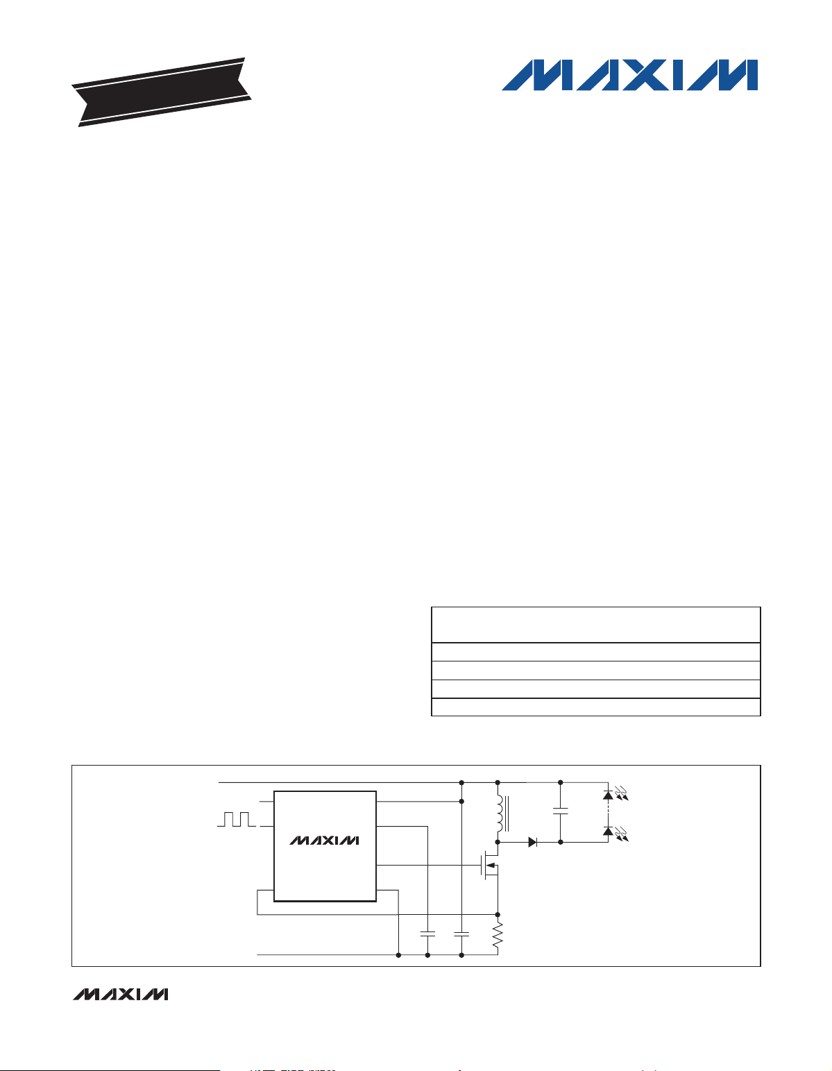
`````````````````````````````````````````````````````````````````````` ࢜ቯᔫ࢟വ
10.8VDC TO 24VDC
ENABLE
PWM
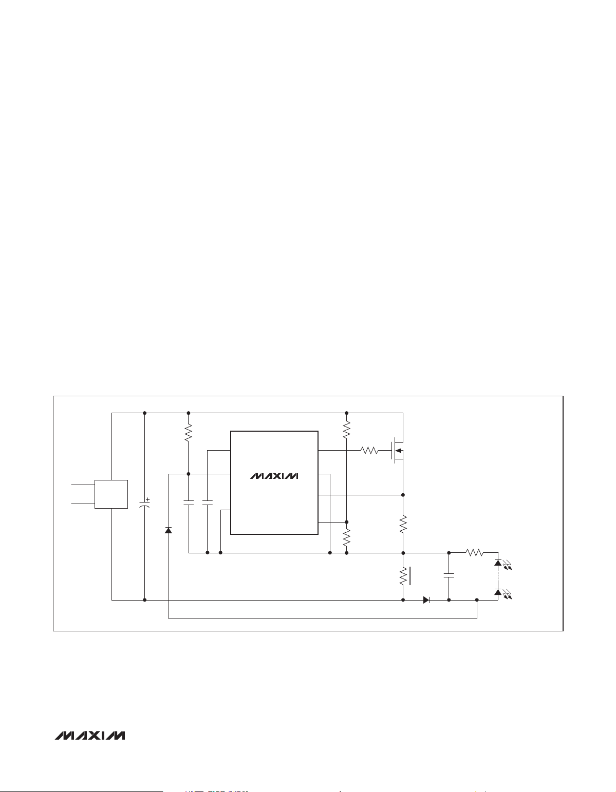
வসǖNBY279120NBY27913ଐᔫ᎖ኹሆLjᓖፀቃቦݷᔫă
________________________________________________________________ Maxim Integrated Products 1
۾ᆪဵ፞ᆪၫᓾ೯ࡼፉᆪLjᆪᒦభถࡀᏴፉࡼݙᓰཀྵࡇᇙăྙኊጙݛཀྵཱྀLj༿Ᏼิࡼଐᒦݬఠ፞ᆪᓾ೯ă
ᎌଥৃĂૡૺࢿ৪ቧᇦLj༿ೊNbyjnᒴሾ၉ᒦቦǖ21911!963!235:!)۱ᒦཌ*Lj21911!263!235:!)ฉᒦཌ*Lj
ᆰNbyjnࡼᒦᆪᆀᐶǖdijob/nbyjn.jd/dpnă
UVLO/EN IN
DIM/FB
MAX16802B
COMP
CS
GND
V
NDRV
GND
LEDs
L1
CC
Q1
C1 R1
C2
C3
D1
᎖ೡࣞMFEདࣅࡼ
ಭሣါĂED.ED!QXN఼ᒜ
ABSOLUTE MAXIMUM RATINGS
IN to GND
V
CC
..........................................................................
to GND
......................................................................
-0.3V to +30V
-0.3V to +13V
DIM/FB, COMP, UVLO/EN, CS to GND....................-0.3V to +6V
NDRV to GND.............................................-0.3V to (V
Continuous Power Dissipation (T
= +70°C)
A
CC
+ 0.3V)
8-Pin μMAX (derate 4.5mW/°C above +70°C) ..............362mW
Stresses beyond those listed under “Absolute Maximum Ratings” may cause permanent damage to the device. These are stress ratings only, and functional
operation of the device at these or any other conditions beyond those indicated in the operational sections of the specifications is not implied. Exposure to
absolute maximum rating conditions for extended periods may affect device reliability.
ELECTRICAL CHARACTERISTICS
(VIN= +12V (MAX16801: VINmust first be brought up to +23.6V for startup), 10nF bypass capacitors at IN and VCC, C
V
UVLO/EN
are at T
UNDERVOLTAGE LOCKOUT/STARTUP
Bootstrap UVLO Wake-Up Level V
Bootstrap UVLO Shutdown Level V
UVLO/EN Wake-Up Threshold V
UVLO/EN Shutdown Threshold V
NBY27912B0C0NBY27913B0C
UVLO/EN Input Current I
UVLO/EN Hysteresis 50 mV
IN Supply Current In
Undervoltage Lockout
IN Voltage Range V
UVLO/EN Propagation Delay
Bootstrap UVLO Propagation
Delay
INTERNAL SUPPLY
VCC Regulator Set Point V
IN Supply Current After Startup I
Shutdown Supply Current UVLO/EN = low 90 μA
GATE DRIVER
Driver Output Impedance
Driver Peak Sink Current 1A
Driver Peak Source Current 0.65 A
PWM COMPARATOR
Comparator Offset Voltage VO
CS Input Bias Current I
Comparator Propagation Delay t
Minimum On-Time t
= +1.4V, V
= +25°C.) (Note 1)
A
PARAMETER SYMBOL CONDITIONS MIN TYP MAX UNITS
= +1.0V, COMP = unconnected, VCS= 0V, TA= -40°C to +85°C, unless otherwise noted. Typical values
DIM/FB
SUVR
SUVF
ULR2
ULF2
UVLO
I
START
t
EXTR
t
EXTF
t
BUVR
t
BUVF
CCSP
IN
R
ON(LOW)
R
ON(HIGH)
PWMVCOMP
CS
PWM
ON(MIN)
VIN rising (MAX16801 only) 19.68 21.6 23.60 V
VIN falling (MAX16801 only) 9.05 9.74 10.43 V
UVLO/EN rising 1.188 1.28 1.371 V
UVLO/EN falling 1.168 1.23 1.291 V
TJ = +125°C 25 nA
VIN = +19V, for MAX16801 only when in
bootstrap UVLO
IN
UVLO/EN steps up from +1.1V to +1.4V 12
UVLO/EN steps down from +1.4V to +1.1V 1.8
VIN steps up from +9V to +24V 5
VIN steps down from +24V to +9V 1
VIN = +10.8V to +24V, sinking 1μA to 20mA
from V
CC
VIN = +24V 1.4 2.5 mA
Measured at NDRV sinking, 100mA 2 4
Measured at NDRV sourcing, 20mA 4 12
- V
CS
VCS = 0V -2 +2 μA
VCS = +0.1V 60 ns
Operating Temperature Range ...........................-40°C to +85°C
Storage Temperature Range ............................-65°C to +150°C
Junction Temperature......................................................+150°C
Lead Temperature (soldering, 10s) .................................+300°C
= 0μF,
NDRV
45 90 μA
10.8 24 V
μs
μs
7 10.5 V
Ω
1.15 1.38 1.70 V
150 ns
2 _______________________________________________________________________________________
᎖ೡࣞMFEདࣅࡼ
ಭሣါĂED.ED!QXN఼ᒜ
ELECTRICAL CHARACTERISTICS (continued)
(VIN= +12V (MAX16801: VINmust first be brought up to +23.6V for startup), 10nF bypass capacitors at IN and VCC, C
V
UVLO/EN
are at T
CURRENT-SENSE COMPARATOR
Current-Sense Trip Threshold V
CS Input Bias Current I
Propagation Delay From
Comparator Input to NDRV
Switching Frequency f
Maximum Duty Cycle D
IN CLAMP VOLTAGE
IN Clamp Voltage V
ERROR AMPLIFIER
Voltage Gain R
Unity-Gain Bandwidth R
Phase Margin R
DIM/FB Input Offset Voltage 3mV
COMP Clamp Voltage
Source Current 0.5 mA
Sink Current 0.5 mA
Reference Voltage V
Input Bias Current 50 nA
COMP Short-Circuit Current 8mA
THERMAL SHUTDOWN
Thermal-Shutdown Temperature 130 °C
Thermal Hysteresis 25 °C
DIGITAL SOFT-START
Soft-Start Duration 15,872
Reference Voltage Steps During
Soft-Start
Reference Voltage Step 40 mV
Note 1: All devices are 100% tested at TA= +85°C. All limits over temperature are guaranteed by characterization.
Note 2: V
Note 3: The MAX16801 is intended for use in universal input offline drivers. The internal clamp circuit is used to prevent the boot-
= +1.4V, V
= +25°C.) (Note 1)
A
PARAMETER SYMBOL CONDITIONS MIN TYP MAX UNITS
is measured with DIM/FB connected to the COMP pin (see the Functional Diagram).
REF
strap capacitor (C1 in Figure 5) from charging to a voltage beyond the absolute maximum rating of the device when
UVLO/EN is low. The maximum current to IN (hence to clamp) when UVLO/EN is low (device in shutdown), must be externally limited to 2mA (max). Clamp currents higher than 2mA may result in clamp voltage higher than +30V, thus exceeding
the absolute maximum rating for IN. For the MAX16802, do not exceed the +24V maximum operating voltage of the device.
= +1.0V, COMP = unconnected, VCS= 0V, TA= -40°C to +85°C, unless otherwise noted. Typical values
DIM/FB
262 291 320 mV
230 262 290 kHz
31 Steps
CS
t
PWM
SW
MAX
INC
REF
CS
VCS = 0V -2 +2 μA
50mV overdrive 60 ns
MAX1680_A 50 50.5
MAX1680_B 75 76
2mA sink current, MAX16801 only (Note 3) 24.1 26.1 29.0 V
= 100kΩ 80 dB
LOAD
= 100kΩ, C
LOAD
= 100kΩ, C
LOAD
High 2.2 3.5
Low 0.4 1.1
(Note 2) 1.218 1.230 1.242 V
= 200pF 2 MHz
LOAD
= 200pF 65 D eg r ees
LOAD
NDRV
= 0μF,
%
V
Clock
cycles
NBY27912B0C0NBY27913B0C
_______________________________________________________________________________________ 3
᎖ೡࣞMFEདࣅࡼ
ಭሣါĂED.ED!QXN఼ᒜ
`````````````````````````````````````````````````````````````````````` ࢜ቯᔫᄂቶ
(V
UVLO/EN
= +1.4V, V
= +1V, COMP = unconnected, VCS= 0V, TA= +25°C, unless otherwise noted.)
DIM/FB
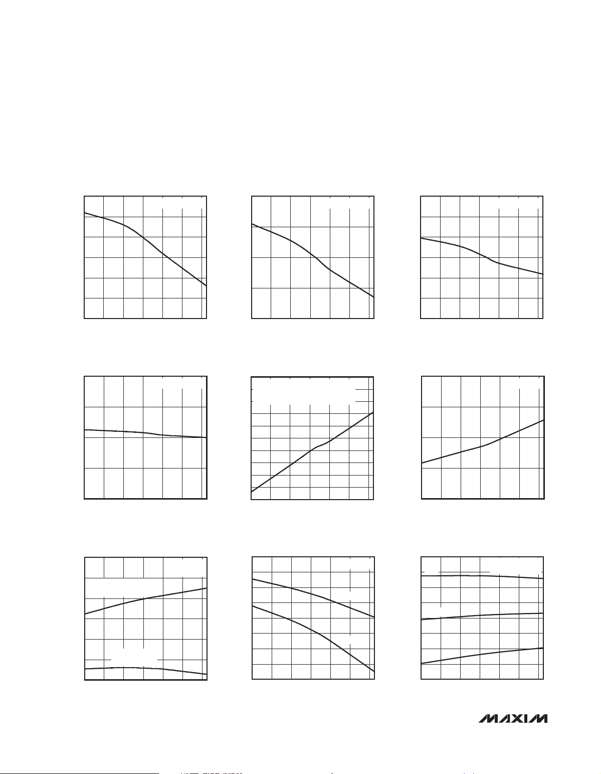
BOOTSTRAP UVLO WAKE-UP LEVEL
vs. TEMPERATURE
21.60
21.55
21.50
(V)
21.45
IN
V
21.40
21.35
21.30
-40 80
MAX16801 VIN RISING
MAX16801 toc01
6040200-20
TEMPERATURE (°C)
UVLO/EN SHUTDOWN THRESHOLD
vs. TEMPERATURE
1.30
NBY27912B0C0NBY27913B0C
1.25
1.20
UVLO/EN (V)
1.15
1.10
-40 80
TEMPERATURE (°C)
UVLO/EN FALLING
MAX16801 toc04
6040200-20
BOOTSTRAP UVLO SHUTDOWN LEVEL
vs. TEMPERATURE
10.1
10.0
(V)
9.9
IN
V
9.8
9.7
-40 80
TEMPERATURE (°C)
VIN SUPPLY CURRENT IN UNDERVOLTAGE
LOCKOUT vs. TEMPERATURE
52
VIN = 19V
51
MAX16801 WHEN IN BOOTSTRAP UVLO
MAX16802 WHEN UVLO/EN IS LOW
50
49
48
(μA)
47
START
I
46
45
44
43
42
-40 80
TEMPERATURE (°C)
MAX16801 VIN FALLING
6040200-20
6040200-20
MAX16801 toc02
MAX16801 toc05
UVLO/EN WAKE-UP THRESHOLD
vs. TEMPERATURE
1.280
1.275
1.270
1.265
UVLO/EN (V)
1.260
1.255
1.250
-40 80
TEMPERATURE (°C)
VIN SUPPLY CURRENT AFTER STARTUP
vs. TEMPERATURE
1.5
1.4
(mA)
1.3
IN
I
1.2
1.1
-40 80
TEMPERATURE (°C)
UVLO/EN RISING
MAX16801 toc03
6040200-20
VIN = 24V
MAX16801 toc06
6040200-20
VCC REGULATOR SET POINT
vs. TEMPERATURE
9.8
9.7
NDRV OUTPUT IS NOT
SWITCHING, V
9.6
(V)
9.5
CC
V
9.4
9.3
9.2
-40 80
NDRV OUTPUT IS
SWITCHING
= 1.5V
DIM/FB
TEMPERATURE (°C)
VIN = 19V
NO LOAD
6040200-20
MAX16801 toc07
(V)
V
VCC REGULATOR SET POINT
vs. TEMPERATURE
8.9
8.8
8.7
8.6
8.5
CC
8.4
8.3
8.2
8.1
-40 80
TEMPERATURE (°C)
VIN = 10.8V
10mA LOAD
20mA LOAD
6040200-20
310
305
MAX116801 toc08
300
295
290
285
280
CURRENT-SENSE THRESHOLD (mV)
275
270
CURRENT-SENSE THRESHOLD
vs. TEMPERATURE
+3σ
MEAN
-3σ
-40 80
TEMPERATURE (°C)
4 _______________________________________________________________________________________
TOTAL NUMBER OF
DEVICES = 100
6040200-20
MAX16801 toc09
᎖ೡࣞMFEདࣅࡼ
ಭሣါĂED.ED!QXN఼ᒜ
``````````````````````````````````````````````````````````````````````````` ࢜ቯᔫᄂቶ)ኚ*
(V
UVLO/EN
PERCENTAGE OF UNITS (%)
(ns)
PWM
t
= +1.4V, V
= +1V, COMP = unconnected, VCS= 0V, TA= +25°C, unless otherwise noted.)
DIM/FB
CURRENT-SENSE THRESHOLD
30
25
20
15
10
5
0
260 320
CURRENT-SENSE THRESHOLD (mV)
TOTAL NUMBER OF
DEVICES = 200
310300290280270
PROPAGATION DELAY FROM
CURRENT-SENSE COMPARATOR INPUT
TO NDRV vs. TEMPERATURE
75
70
65
60
55
50
-40 80
TEMPERATURE (°C)
6040200-20
280
+3σ
275
MAX16801 toc10
270
265
MEAN
260
255
250
SWITCHING FREQUENCY (kHz)
MAX16801 toc13
-3σ
245
240
-40 80
14
13
12
11
10
9
8
7
6
5
4
3
2
UNDERVOLTAGE LOCKOUT DELAY (μs)
1
0
-40 80
SWITCHING FREQUENCY
vs. TEMPERATURE
TOTAL NUMBER OF
DEVICES = 100
6040200-20
TEMPERATURE (°C)
UVLO/EN PROPAGATION DELAY
vs. TEMPERATURE
UVLO/EN RISING
UVLO/EN FALLING
6040200-20
TEMPERATURE (°C)
30
25
MAX16801 toc11
20
15
10
PERCENTAGE OF UNITS (%)
5
0
230 290
1.230
VIN = 12V
1.229
MAX16801 toc14
1.228
1.227
REFERENCE VOLTAGE (V)
1.226
1.225
-40 80
SWITCHING FREQUENCY
TOTAL NUMBER OF
DEVICES = 200
SWITCHING FREQUENCY (kHz)
REFERENCE VOLTAGE
vs. TEMPERATURE
TEMPERATURE (°C)
280270260250240
6040200-20
NBY27912B0C0NBY27913B0C
MAX16801 toc12
MAX16801 toc15
INPUT CURRENT
vs. INPUT VOLTAGE
10
9
8
7
6
5
4
INPUT CURRENT (mA)
3
2
1
0
10.0 30.0
INPUT VOLTAGE (V)
_______________________________________________________________________________________ 5
INPUT CLAMP VOLTAGE
vs. TEMPERATURE
27.0
26.8
MAX16801 toc16
26.6
26.4
26.2
26.0
25.8
25.6
INPUT CLAMP VOLTAGE (V)
25.4
25.2
27.525.020.0 22.515.0 17.512.5
25.0
-40 80
TEMPERATURE (°C)
IIN = 2mA
6040200-20
MAX16801 toc17
2.2
2.1
2.0
1.9
1.8
(Ω)
1.7
ON
R
1.6
1.5
1.4
1.3
1.2
NDRV OUTPUT IMPEDANCE
vs. TEMPERATURE
VIN = 24V
SINKING 100mA
-40 80
TEMPERATURE (°C)
6040200-20
MAX16801 toc18
᎖ೡࣞMFEདࣅࡼ
ಭሣါĂED.ED!QXN఼ᒜ
```````````````````````````````````````````````````````````````````````````` ࢜ቯᔫᄂቶ)ኚ*
(V
UVLO/EN
= +1.4V, V
= +1V, COMP = unconnected, VCS= 0V, TA= +25°C, unless otherwise noted.)
DIM/FB
NDRV OUTPUT IMPEDANCE
5.0
4.8
4.6
4.4
4.2
(Ω)
4.0
ON
R
3.8
3.6
3.4
3.2
3.0
-40 80
vs. TEMPERATURE
VIN = 24V
SOURCING 20mA
TEMPERATURE (°C)
MAX16801 toc19
6040200-20
ERROR-AMPLIFIER OPEN-LOOP GAIN
120
100
GAIN (dB)
-20
-40
-60
-80
-100
AND PHASE vs. FREQUENCY
80
60
40
20
0 -70
0.1 100M
GAIN
PHASE
FREQUENCY (Hz)
MAX16801 toc20
50
30
10
-10
-30
-50
-90
PHASE (DEGREES)
-110
-130
-150
-170
10M1M10k1k 100k10 1001
`````````````````````````````````````````````````````````````````````````` ୭ႁී
୭
NBY27912B0C0NBY27913B0C
1 UVLO/EN
2 DIM/FB
3 COMP
߂ ถ
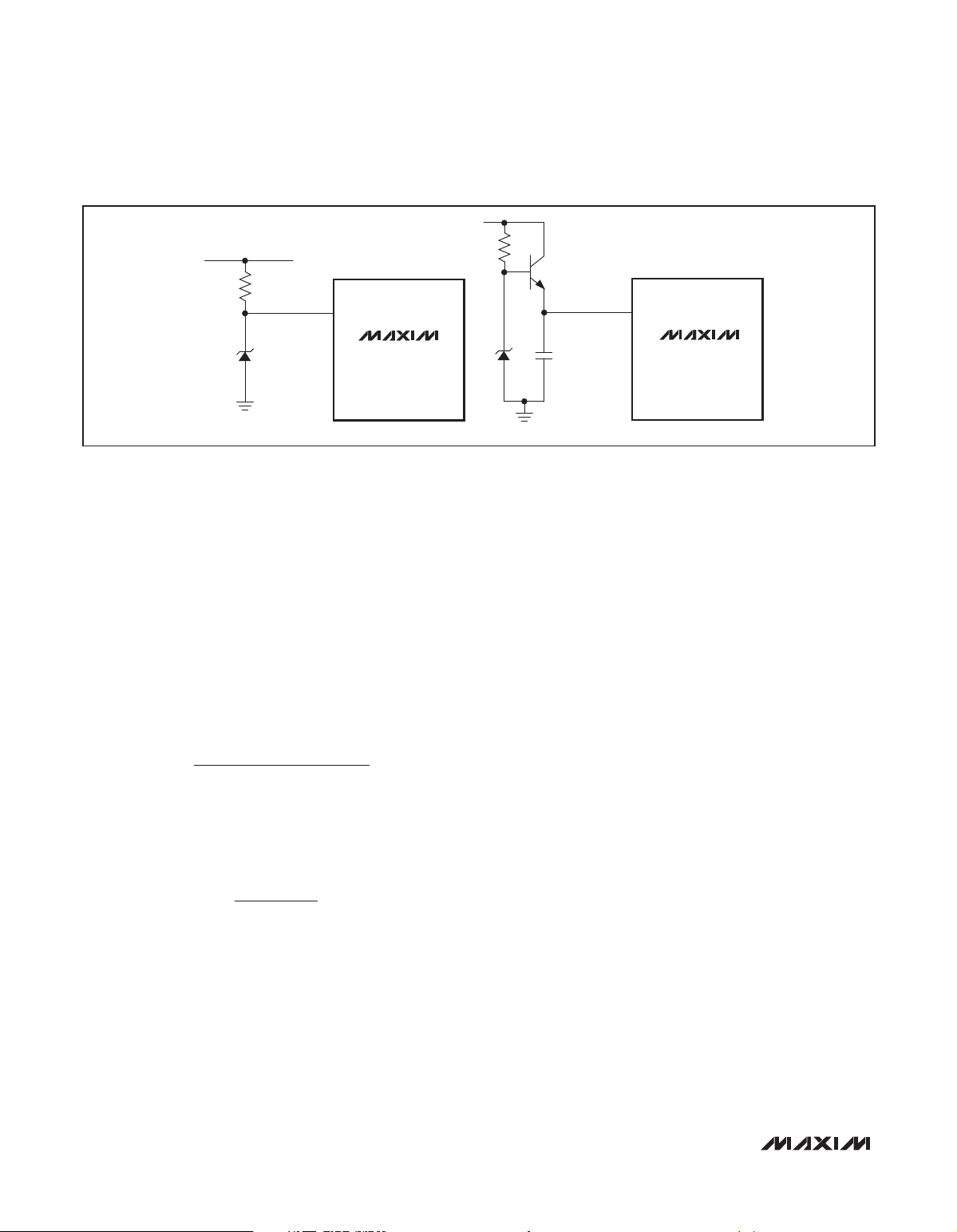
ᅪݝభܠ߈་ኹჄࢾăVWMPᒙၒྜྷࣅ࢟ኹăVWMPೌᒗHOEభணᒏୈᔫă
ࢅຫQXNೡࣞࢯஂၒྜྷ0ᇙތࡍሤၒྜྷ࣡ă
ᇙތࡍၒ߲ăᏴறࣞMFE࢟ഗࢯஂ።ᒦLjݗޡᏄୈೌᏴEJN0GCDPNQᒄମă
4CS
5 GND
6 NDRV
7V
CC
࢟ഗঢ።ቧೌ࣡Lj᎖࢟ഗࢯஂăᒗଶഗ࢟ᔜ࣡ăభጲSD݆߹བྷ༄ዘࡼඇࠦă
࢟Ꮞă
ᅪݝoࡸNPTGFUᐜೌ࣡ă
ᐜདࣅ࢟ᏎăดݝᎅJOଢ଼ኹࡻࡵăW
ᎧHOEମጙᒑ21oGྏᒋৎࡼབྷẮ࢟ྏă
DD
JD࢟ᏎăJOᎧHOEମጙᒑ21oGྏᒋৎࡼབྷẮ࢟ྏăᔈᔫෝါ)NBY27912*ሆLjభᏴၒྜྷ࢟Ꮞ
8IN
JOᒄମጙৈࣅ࢟ᔜăມᒙླྀᔝ࢟Ꮞೌᒗক࢛)ݬᅄ6*ă࣪᎖NBY27913LjJOᒇ,21/9Wᒗ,35W
࢟Ꮞă
``````````````````````````````` ሮᇼႁී
NBY279120NBY27913ᇹୈ᎖ೡࣞ)IC*! MFEࡼ
ഗདࣅLjးᄰᑍීመာ።ăকᇹୈᓜᆐ
ಭಭ࢟വᅠແଐLjྙcvdlĂcpptuĂgmzcbdl
TFQJDࢀLjᔫᏴೌኚೌኚෝါăఎຫൈᏴดݝᆈ
ࢯᆐ373lI{ৼࢾᒋLjభဣሚ࢟ഗෝါ఼ᒜăᎌ୷ᒣ
ૄ࢟ኹ)22/:W*ࡼᔈVWMP࢟വĂިࢅࣅ࢟ഗጲૺࢅ
ᔫ࢟ഗᄂቶLjభဣሚࡼᄰၒྜྷMFEདࣅăকᇹ
ୈ߹ดᒙᔈVWMPᅪLjથถᄰVWMP0FO୭࣪ၒྜྷ
ࣅ࢟ኹቲܠ߈ᒙăNBY27912ޟးᄰୣഗၒ
ྜྷ)96WBDᒗ376WBDᑳഗ࢟ኹၒྜྷ* དࣅăNBY27913
ޟးࢅၒྜྷ࢟ኹ)21/9WEDᒗ35WED*።ă
NBY279120NBY27913ᓆᒲ໐ପ၁ഗᅪݝNPTGFUࡼ࢟
ഗLj࠭ဣሚ࣪MFE࢟ഗࡼࢯஂă
6 _______________________________________________________________________________________
᎖ೡࣞMFEདࣅࡼ
ಭሣါĂED.ED!QXN఼ᒜ
ࡩᔫᏴࡒᎌܤኹࡼᔈෝါဟ)ᅄ6*Ljক࢟വથభᄋ
ࡍࣶၫവ৺ᑇۣઐăࡩ߲ሚവ৺ᑇဟLjྯླྀᔝ
࢟ኹଢ଼ᒗ,21WጲሆLjᒘဧVWMP࢟വܕᅪݝ
NPTGFUࡼᐜདࣅቧăᑚ્ᒮቤ߿ጙࠨྟࣅ߈ă
ྦኊገறමࢯஂMFE࢟ഗLjభಽຢᇙތࡍጲૺற
ࣞᆐ2&ࡼᓰ)ᅄ:*ăᑚጙᅪౣభࡍࡍଢ଼ࢅᎅ᎖ᇄᏎ
ᏄୈܤછມތჅޘညࡼ፬ሰLj݀༦ᒑኊᔢࡼᅪᆍᏄ
ୈ૾భဣሚă
ࢅຫQXNೡࣞࢯஂቧᒇౣྜྷEJN0GC୭భဣሚ
ᆍࡼೡࣞࢯஂă
᎖NBY27912ଐࡼMFEདࣅ࢟വݧጙৈᒋࣅ࢟
ᔜS2ᆐถ࢟ྏD2ߠ࢟)ᅄ6ᅄ:*ăᏴ߱ဪࣤLjߠ࢟
࢟ኹࢅ᎖ดݝᔈVWMPඡሢ࢟ኹLjୈሿࡼஸზ࢟ഗ
ஞᆐ56μB )࢜ቯᒋ*ăࢅࣅ࢟ഗ୷ᒣૄ࢟ኹࡼᔈ
VWMPభࡍࡍଢ଼ࢅS2ࡼLj૾ܣဵᏴᄰୣഗၒྜྷ࢟ኹ
ᆡ᎖࣡ဟጐቃă
ࡩበຢஉᆨި,241°D )࢜ቯᒋ*ဟLjดᒙࡼࣥ࢟വభ
ࣅۣઐถă
ೡࣞࢯஂ
ሣቶೡࣞࢯஂဵᄰᏴDTࡼጙৈཇஂ࢛ဣሚࡼLj
ྙᅄ7ᅄ8Ⴥာă
ࢅຫQXN )࢟ഗᐮ݆*ೡࣞࢯஂᐌᄰᏴୈࡼEJN0GC
୭ဗଝጙৈሤ൝QXNቧဣሚ)ᅄ9*ăᑚᒬ
࣪᎖กቋገཇࢯஂೡࣞဟዏৃۣߒໍݙܤࡼ።ޝ
ጐ્ဵ၅ኡښăဵᄰ࣪ࢾࣞࡼMFE࢟ഗቲ
ᐮ݆ဣሚࢯࡼă
NBY279120NBY27913ࡼມᒙ
ࡩܤኹࡀᏴဟLjᎅܤኹဣሚᔈ)ᅄ6*ăݧಭ
ါᅠແဟጐభᒇᎅMFEޘညມᒙ)ᅄ2*ă
NBY27912B0C0NBY27913B0C
R1
V
CC
IN GND
AC
IN
BRIDGE
RECTIFIER
COMP
C1
C2 C3
DIM/FB
ᅄ2/! ᏴಭቯgmzcbdlདࣅᒦಽMFEᆐJDᄋມᒙ
MAX16801B
NDRV
UVLO/EN
R5
R2
CS
R6
Q1
R3
R4
L1
C4
D3
TOTAL LED VOLTAGE:
11V TO 23V
_______________________________________________________________________________________ 7
᎖ೡࣞMFEདࣅࡼ
ಭሣါĂED.ED!QXN఼ᒜ
VDC
VDC
R
IN
D
(a)
ᅄ3/! )b*࢟ᔜ.ฃ)c*ᄏ.ฃ.࢟ᔜມᒙ࢟വ
MAX16802A
NBY27913భᒇᎅ21/9WEDᒗ35WEDၒྜྷ࢟ኹቲມᒙă
ಽ࢟ᔜ.ฃ)ᅄ3b*ᄏ.ฃ.࢟ᔜ
ມᒙ࢟വ)ᅄ3c*LjNBY27913ጐభᏴৎᒇഗၒྜྷ࢟
ኹࡼޝă
NBY279120NBY27913་ኹჄࢾ
NBY27912B0C0NBY27913B0C
NBY279120NBY27913ᎌጙৈၒྜྷ࢟ኹVWMP0FO୭ă
VWMPඡሢ࢟ኹᆐ,2/39WăᒑᎌᏴক୭࢟ኹࡍ᎖,2/39W
ઁ࢟വݣఎဪᔫăVWMP࢟വభဧDQXN܈୷ĂJMJN
܈୷Ăᑩጲૺၒ߲དࣅࠀ᎖ࣥᓨზLjጲି
࢟ഗሿ)ݬ
ࣅ࢟ኹăኹ࢟ᔜS3S4 )ᅄ6*ᔜᒋࡼଐႯါྙሆǖ
ถౖᅄ
*ăಽকVWMPถభᒙၒྜྷ
R
Q
IN
DC
(b)
MAX16802A
NBY27912ᔈ་ኹჄࢾ
߹೫NBY279120NBY27913ᎌࡼᅪݝభܠ߈VWMPᅪLj
NBY27912થดᒙጙৈᅪࡼᔈVWMPLjᏴଐኹ
MFEདࣅဟޟᎌ)ݬ
߱ဪ࢟ဟᔈቲࣅăࡩW
,34/7WဟLjNBY27912ఎဪࣅăࣅ໐ମLjVWMP࢟വ
ۣߒDQXN܈୷ĂJMJN܈୷Ăᑩጲૺၒ߲དࣅ
ࠀ᎖ࣥᓨზLjጲିቃ࢟ഗሿăጙࡡW
VWMP࢟വࣅDQXN܈୷ĂJMJN܈୷ᑩLj݀
Ꮴၒ߲དࣅఎဪఎݷᔫăྙW
VWMP࢟വᐌࣥDQXN܈୷ĂJMJN܈୷Ăᑩጲ
ૺၒ߲དࣅLj࠭ဧNBY27912ૄᒗࣅෝါă
ถౖᅄ
JO
*ăᑚዹᏤୈᏴ
᎖ᔈVWMPඡሢ࢟ኹ
ࡉࡵ,34/7WLj
JO
ଢ଼ᒗ,:/8WጲሆLj
JO
VV
R
3
≅
500
ULR IN
IVV
×
UVLO IN ULR
ኡᐋS4ᔜᒋဟLj።ဧVWMP0FOၒྜྷມᒙ࢟ഗᏴS3ࡼኹ
ଢ଼ჅޘညࡼᇙތᔢࢅăW
)ᔢࡍᒋ*LjW
ဵ࢟Ꮞࣅဟࡼၒྜྷ࢟Ꮞ࢟ኹᒋă
JO
VV
IN ULR
R
23
=×
×
2
−
()
> ,2/39WLjJ
VMS3
−
2
V
ULR
2
2
> 61oB
VWMP
R
NBY27912ࣅᔫෝါ
ᏴಭါMFEདࣅ።ᒦLjWJOནᔈܤኹࡼྯླྀᔝă
Ljࣅဟܤኹᒦᎌ࢟ถᄋăፐࠥLjኊገᄂࢾ
ࡼᔈ߈ăᅄ4ჅာᆐࣅဟJOW
ఎဪLjW
JOWDD
S2D2ߠᒗ෭ৈᒦମ࢟ኹăࠥဟLjดݝᆮኹఎဪሶD3
ߠ࢟ )ݬᅄ6*ăᏴᎅS2ᄋࡼ࢟ഗࡩᒦLjNBY27912ஞ
56μBLjၒྜྷ࢟ഗᐌᆐD2D3ߠ࢟ăࡩW
ᆐ1Wăဗଝ࢟Ꮞ࢟ኹᒄઁLjࣅ࢟ᔜ
႒ᆐ,:/6WဟLjᄫᒏ࣪D3ߠ࢟LjD2ೝ࣡ࡼ࢟ኹଖኚဍLj
ᒦJ
ဵVWMP0FO୭ࡼၒྜྷ࢟ഗLjW
VWMP
ဵVWMP0FO
VMS3
ታඡሢă
8 _______________________________________________________________________________________
ᒇࡵক࢟ྏࡼ࢟ኹࡉࡵታ࢟ኹ,34/7WᆐᒏăጙࡡW
ࡍ᎖ᔈVWMPඡሢ࢟ኹLjOESWఎဪఎNPTGFULj݀
୭ࡼ࢟ኹă
DD
࢟ኹத
DD
JO
᎖ೡࣞMFEདࣅࡼ
ಭሣါĂED.ED!QXN఼ᒜ
V
CC
2V/div
MAX16801
PIN
V
IN
5V/div
0
100ms/div
ᅄ4/! ࡩNBY27912ࠀ᎖ᔈෝါሆLjࣅဟࡼWJOW
DD
ሶླྀᔝྯླྀᔝࠅၒ࢟ถăྙྯླྀᔝၒ߲
ೂ࢟ኹ᎖,:/8W )ᔈVWMPࢅ࣡ඡሢ*Ljᐌࣅ߈ᅲ
߅Ljఎဪೌኚᔫă
ྙᏴࣅᅲ߅ᒄ༄W
ଢ଼ᒗ,:/8WጲሆLjᐌୈૄᒗ
JO
ࢅ࢟ഗVWMPᓨზăᑚᒬ༽ౚሆLjభᐐࡍD2ࡀᔗ৫ࡼ
࢟ถLjጲܣྯླྀᔝೂᔗ৫ࡼ࢟ኹă
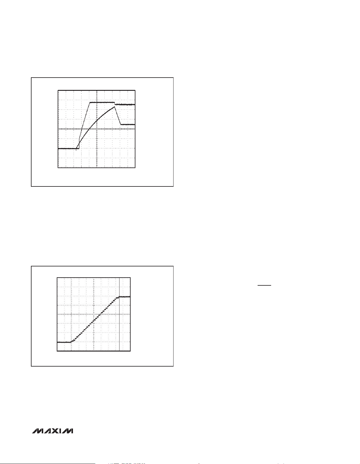
````````````````````````````````` ྟࣅ
NBY279120NBY27913ࡼྟࣅᄂቶభဧMFE࢟ഗᏴ၊఼
ෝါሆዘቓຸဍăࡩᅙಭVWMPᓨზઁఎဪྟࣅ߈ă
ଝᒗࡍᄴሤஂ࢛ࡼ࢟ኹᏴ71ntࡼྟࣅဟମด࠭1ᒇ
ሣဍᒗ,2/34Wăᅄ5መာ೫1/6Bࡼ࢜ቯၒ߲࢟ഗᏴࣅ
߈ᒦࡼܤછ༽ౚăభᓖፀࡵMFE࢟ഗጲᄇါဍă
ᑚဵᎅ᎖ݧ೫ၫᔊྟࣅଆၣăᎧୈݙᄴࡼဵLj
ดᒙࡍࡼᓰ࢟ኹဵྟࣅࡼăᑚᒬถ୷
఼ᒜMFE࢟ഗă
oࡸNPTGFUఎདࣅ
OESW୭ถདࣅᅪݝoࡸNPTGFUăOESWၒ߲ᎅดݝ
ᆮኹ)W
࣪᎖ᄰၒྜྷ࢟ኹࡒᎌܤኹࡼ።ዔLjჅݧࡼ
NPTGFUܘኍถߌ၊࢟Ꮞ࢟ኹᔢဟࡼᒇഗ࢟ຳᎧܤኹ
߱ࡼ࢟ኹᒄă࣪᎖ࡍࣶၫݧೌኚgmzcbdlᅠແ
ࡼಭሣါ።ዔLjኊገࢾ࢟ኹᆐ711WࡼNPTGFUă
OESWถᏎ߲0ᇢྜྷި761nB02111nBᒋ࢟ഗăჅኡᐋ
ࡼNPTGFUޘညࡼࡴᄰႼఎႼܘኍᏴభ၊ࡼ
ᆍดă
NBY279120NBY27913۞౪ጙৈดݝᇙތࡍLjభ
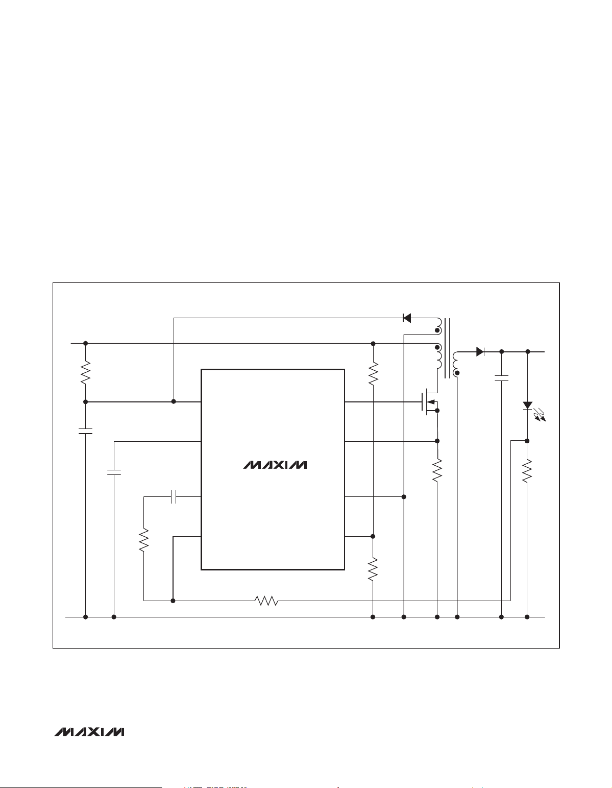
ޟறཀྵࢯஂMFE࢟ഗăಿྙLjᅄ6Ⴥာࡼಭါ࢟
ᏎăMFE࢟ഗࡼଐႯါྙሆǖ
*࢟LjকดݝᆮኹᏴดݝᒙᆐᏖ,:/6Wă
DD
ดݝᇙތࡍ
NBY27912B0C0NBY27913B0C
0
10ms/div
ᅄ5/! ߱ဪࣅဟࡼ࢜ቯྟࣅ࢟ഗ
_______________________________________________________________________________________ 9
100mA/div
V
REF
=
R
7
ᒦW
I
LED
> ,2/34Wăࡍࡼᄴሤၒྜྷ࣡ᎅดݝೌᒗ
SFG
ၫᔊྟࣅ࢟വLjཀྵۣࣅ߈ᒦᓰ࢟ኹદൻဍLj
݀কᓰ࢟ኹဗଝᒗক୭ăᑚዹభ༓ᒜMFE࢟ഗᏴჅ
ᎌᓨზሆ࣒ږᑍᎾࢾࡼါᎌኔဍă

᎖ೡࣞMFEདࣅࡼ
ಭሣါĂED.ED!QXN఼ᒜ
``````````````````````````````` ።ቧᇦ
NBY27912᎖ೡࣞMFEདࣅ
ࡼࣅဟମఠ
JOവ࢟ྏD2᎖Ᏼ࢟വধধታဟኸႥᄋᔫ࢟ഗ
)ᅄ6*ăD2ࡼߛࡁྯླྀᔝࡼೌါࢾ೫భ᎖
ࣅࡼᒲ໐ၫăࡍྏᒋD2ዓޠ೫ࣅဟମLjࡣถᏴ߱ဪ
ࣅࣤᄋৎࣶ࢟ጲᑽߒৎࣶࡼఎᒲ໐ăྙD2ࡼ
ྏᒋვቃLjกඐOESWᎌᔗ৫ࡼဟମఎNPTGFULj
࠭ݙถᏴྯླྀᔝೂᔗ৫ࡼ࢟ኹᆐୈᄋ࢟ᏎLj
ᒘဧW
D2D3ኊݧࢅቛധ࢟ྏă
ଣࢾᏴࢅ࢟Ꮞ࢟ኹᓨზሆ )96WBDၒྜྷࡼᄰಭሣါ።*
ಭሣါMFEདࣅ྆ገᆒߒቃ᎖611ntࡼࣅဟମLjࣅ
࢟ᔜS2።ถᄴဟᄋୈჅኊࡼᔢࡍࣅມᒙ࢟ഗ)ᔢތ
ᓨზሆ:1μ B*ᆐD2ĂD3ߠ࢟Ⴥኊࡼ࢟ഗăᏴᎾ໐ࡼ
611ntࣅဟମดLjവ࢟ྏD3ܘኍۻߠ࢟ࡵ,:/6WLj
D2ܘኍߠ࢟ࡵ,35Wă
ᎅ᎖NBY27912ดݝᎌ71ntࡼྟࣅဟମLjD2ܘኍࡀᔗ
NBY27912B0C0NBY27913B0C
৫ࡼ࢟LjጲܣᒗᏴᑚࣤဟମดሶୈ።࢟ഗă
ጲሆါத႒ଐႯჅኊࡼ࢟ྏᒋǖ
ᒦJ
ဵR2ࡼᔐᐜ࢟LjgTXဵNBY27912ࡼఎຫൈ)373lI{*Lj
W
ମ)71nt*ă
ಿྙǖ
ଢ଼ᒗ,:/8WጲሆăୈૄVWMPᓨზݙถࣅă
JO
IQ f
=×
g gtot SW
C
=
1
ဵࣅઁNBY27912ࡼดݝ࢟Ꮞ࢟ഗ)2/5nB*LjR
JO
ဵᔈVWMPᒣૄ࢟ኹ)22/:W*LjuTTဵดݝྟࣅဟ
IZTU
8 262 2 1
Ig nC kHz mA
()( ) .
=× =
14 21 60
mA mA ms
..
()
1
C
=
IIt
+
()
IN g SS
+
()
V
HYST
×
()
12
V
()
=μ
17 5
.
hupu
F
ଣ D2 ? D3LjᐌږጲሆါଐႯS2ǖ
×
VC
SUVR
=
I
C
1
500
()
VV
IN MIN SUVR
1
=
R
ᒦW
VWMPታ࢟ຳ)ᔢࡍᒋ,34/7W*LjJ
Ꮞ࢟ഗ)ᔢࡍᒋ:1μB*ă
ಿྙLjୣഗၒྜྷ࢟ኹནᔢቃᒋ96WဟLjᎌǖ
࢟ᔜནܪᓰᒋ231lΩă
ྙᏤৎޠࡼࣅဟମLjᐌS2ᔜᒋభኡནࡻ܈ၤଐ
ႯᒋৎࡍጙቋLjᑚዹభጲଢ଼ࢅক࢟ᔜࡼă
ၤࣅښభ᎖ಢ႒᎖ᅄ6ࡼ࢟വăক࢟വᒦྯླྀ
ᔝᎧၒ߲ླྀᔝᄴሤăፐྀဟମྯླྀᔝࡼ࢟ኹᎧၒ
߲࢟ኹᔐ߅ᑵ܈Lj݀ၒ߲࢟ኹள಼ሤᄴࡼྟࣅ߈ă
D2࠭,33W࢟ᒗ,21Wࡼᔢ࢟ဟମܘኍࡍ᎖71ntࡼྟ
ࣅဟମă
ဣሚᔈࡼጙৈဵᏴࢯஂၒ߲࢟ኹࡼླྀᔝᒄᅪݧ
ጙৈࣖೂࡼມᒙླྀᔝLj݀ဧມᒙླྀᔝᎧNPTGFUࡴᄰဟ
ମᄴሤ)ݬᅄ:*ăᏴࠥ༽ౚሆLjჅኊࡼ࢟ྏᒋቃࣶ೫ă
LjᏴᑚᒬါሆLjၒྜྷ࢟ኹᆍܘኍቃ᎖3;2ăᏴ
ࢾມᒙླྀᔝဵᎧၒ߲ᄴሤဟLjથᎌጙৈኊገఠࡼ
ᆰᄌăྙᄴሤLjᐌMFEདࣅ࢟വ્Ᏼၒ߲വᓨზሆࡌ
ᡅྟࣅăࡣဵLjྙມᒙླྀᔝᎧNPTGFUࡴᄰဟମᄴ
ሤLjݙᎌকᄂቶă
ဵ።ᒦࡼᔢቃၒྜྷ࢟ኹLjW
JO)NJO*
24 15
×
VμF
()
I
=
C1
1
R
500
()
120
=
V
072 90
mA A
.()+μ
()
1
ms
−
()
+
II
C START
1
TUBSU
()
ms
−
224
072
=
.
V
=Ω
ဵᔈ
TVWS
ဵࣅဟJOࡼ࢟
mA
119
k
࢟ྏᒋནܪᓰᒋ26μGă
10 ______________________________________________________________________________________
᎖ೡࣞMFEདࣅࡼ
ಭሣါĂED.ED!QXN఼ᒜ
።࢟വ
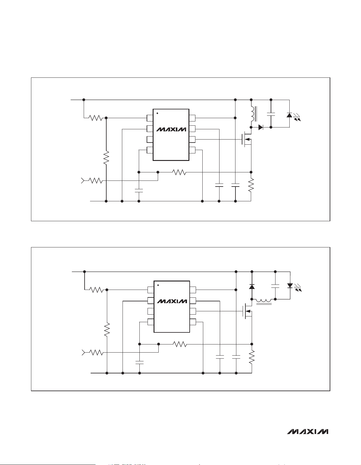
ᅄ6߲೫ጙৈ᎖NBY27912ࡼಭሣါIC! MFEདࣅ።
࢟വăܤኹU2భࡍࡍᄋଐࡼഉቶăดݝᇙތ
ࡍభဣሚޟறཀྵࡼMFE࢟ഗ఼ᒜă
ᅄ7߲೫ጙৈᎌሣቶೡࣞࢯஂถࡼೌኚgmzcbdl
MFEདࣅăMFEᔐ࢟ኹభࢅ᎖᎖ၒྜྷ࢟ኹă
V
SUPPLY
R1
IN
ᅄ8߲೫ጙৈೌኚࡴᄰෝါࡼIC! MFE! cvdlདࣅLj
ᎌሣቶࢯLjᒑኊࡼᅪݝᏄୈă
ᅄ9߲೫ጙৈ᎖NBY27912ĂݧࢅຫQXNါࢯ
ࡼಭሣါಭgmzcbdl IC MFEདࣅăQXNቧኊገሤ
)ݬ
ถౖᅄ
*ăܤኹU2ᄋڔཝಭLjᔫ᎖ᄰୣ
ഗ࢟Ꮞ)96WBDᒗ376WBD*ă
D1
R2
NDRV
T1
D2
C4
Q1
V
OUT
LEDs
NBY27912B0C0NBY27913B0C
C1
V
CC
C2
C3
COMP GND
R6
GND
ᅄ6/! ಭሣါĂಭĂgmzcbdl!MFEདࣅLjᎌభܠ߈ၒྜྷࣅ࢟ኹ
DIM/FB UVLO/EN
MAX16801
R5
CS
R7R4
R3
______________________________________________________________________________________ 11
᎖ೡࣞMFEདࣅࡼ
ಭሣါĂED.ED!QXN఼ᒜ
V
IN
10.8V TO 24V
R1
R2
DIMMING
ᅄ7/! ᎌೡࣞࢯஂถࡼNBY27913! gmzcbdl!IC! MFEདࣅLjၒྜྷ࢟ኹᆍ21/9Wᒗ35W
NBY27912B0C0NBY27913B0C
10.8V TO 24V
R3
GND
V
IN
R1
R2
UVLO/EN
DIM/FB
COMP
UVLO/EN
DIM/FB
COMP
1
2
MAX16802B
3
CS
4
R4
C1
1
2
MAX16802B
3
CS
4
IN
8
V
CC
7
NDRV
6
GND
5
IN
8
V
CC
7
NDRV
6
GND
5
C2 C3
L1
C4
D1
Q1
R5
D1
C4
L1
Q1
LED(s)
LED(s)
R3
DIMMING
C1
GND
R4
C2 C3
R5
ᅄ8/! ᎌೡࣞࢯஂถࡼNBY27913! cvdl!IC! MFEདࣅLjၒྜྷ࢟ኹᆍ21/9Wᒗ35W
12 ______________________________________________________________________________________
᎖ೡࣞMFEདࣅࡼ
ಭሣါĂED.ED!QXN఼ᒜ
UNIVERSAL
AC INPUT
BRIDGE
RECTIFIER
OPTIONAL ONLY WHEN PWM DIMMING IS USED
C4
R1
C3
V
CC
IN
MAX16801B
C1
*PWM
*WARNING: PWM DIMMING SIGNAL IS SHOWN AT THE PRIMARY SIDE.
USE AN OPTOCOUPLER FOR SAFETY ISOLATION OF THE PWM SIGNAL.
C2
DIM/FB UVLO/EN
NDRV
GND
NBY27912B0C0NBY27913B0C
D1D3
R2
CS
R3
T1
D2
Q1
LEDs
C6
R4
C5
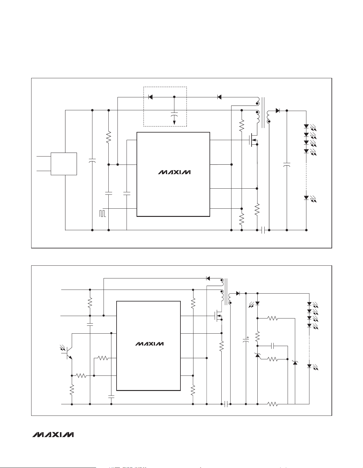
ᅄ9/! ᄰୣഗၒྜྷĂಭሣါĂಭቯgmzcbdl! IC!MFEདࣅLjݧࢅຫQXNࢯ
D1
+V
IN
U2
OPTO TRANS
GND
R1
IN
C1
V
CC
R7
COMP GND
R5
R6
DIM/FB UVLO/EN
C2
MAX16801
R2
NDRV
CS
R3
ᅄ:/! ᄰၒྜྷĂಭሣါĂಭቯgmzcbdl! IC!MFEདࣅLjᎌறࣞ࢟ഗࢯஂᄂቶ
T1
D3
Q1
C4
R4
C5
V
OUT
OPTO LED
R11
U3
TLV431
U2
R8
C3
R9
R10
Z1
______________________________________________________________________________________ 13
᎖ೡࣞMFEདࣅࡼ
ಭሣါĂED.ED!QXN఼ᒜ
`````````````````````````````````````````````````````````````````````````` ถౖᅄ
V
CC
UVLO/EN
COMP
IN
IN
CLAMP
26.1V
BOOTSTRAP UVLO**
DIGITAL
SOFT-START
REFERENCE
1.23V
21.6V
9.74V
1.28V
1.23V
UVLO
IN
REGULATOR
REG_OK
V
CC
V
L
(INTERNAL 5.25V SUPPLY)
DIM/FB
ERROR
AMP
CPWM
LIM
*OSCILLATOR
262kHz
MAX16801
V
0.3V
1.38V
CS
V
OPWM
NBY27912B0C0NBY27913B0C
CS
MAX16802
``````````````````````````````` ኡቯᒎฉ
STARTUP
VOLTAGE
(V)
PART
BOOTSTRAP
UVLO
MAX16801A Yes 22 50
MAX16801B Yes 22 75
MAX16802A No 10.8* 50
MAX16802B No 10.8* 75
*
NBY27913ᎌดݝᔈVWMPă
୭࢟ኹ᎖,8W )JO୭࢟ኹᆐ,21/9Wဟࡼۣᑺၒ߲*Lj
W
DD
݀༦VWMP0FO୭ᆐ࢟ຳဟNBY27913ఎဪᔫă
MAX DUTY
CYCLE (%)
DRIVER
S
Q
R
THERMAL
SHUTDOWN
*MAX16801A/MAX16802A: 50% MAXIMUM DUTY CYCLE
MAX16801B/MAX16802B: 75% MAXIMUM DUTY CYCLE
**MAX16801 ONLY
NDRV
GND
``````````````````````````````` ୭ᒙ
TOP VIEW
UVLO/EN
DIM/FB
COMP
1
2
MAX16801
3
MAX16802
CS
4
μMAX
IN
8
V
7
CC
6
NDRV
GND
5
14 ______________________________________________________________________________________

᎖ೡࣞMFEདࣅࡼ
ಭሣါĂED.ED!QXN఼ᒜ
```````````````````````````````````````````````````````````````````````````` ᓤቧᇦ
ྙኊᔢதࡼᓤᅪተቧᇦݚLj༿އኯ china.maxim-ic.com/packagesă༿ᓖፀLjᓤܠ൩ᒦࡼĐ,đĂĐ$đĐ.đஞܭာSpITᓨზă
ᓤᅄᒦభถ۞ݙᄴࡼᆘᓮᔊLjࡣᓤᅄᒑᎧᓤᎌLjᎧSpITᓨზᇄă
ᓤಢቯ
8 μMAX — 21-0036
ᓤܠ൩
ᆪܠ
NBY27912B0C0NBY27913B0C
______________________________________________________________________________________ 15

᎖ೡࣞMFEདࣅࡼ
ಭሣါĂED.ED!QXN఼ᒜ
```````````````````````````````````````````````````````````````````````````` ኀࢿ಼ဥ
ኀࢿ ኀࢿ྇໐ ႁී ኀখ
0 10/05 —
1 1/06 1
2 1/10 1, 2, 3, 6–15
ᔢ߱ۈ۾ă
ᐐଝ೫NBY27913BFVB,ୈă
ৎᑵ೫ଐႯါLjৎቤ೫ሆܪLj݀࿎߹೫ᓤᅄă
NBY27912B0C0NBY27913B0C
Nbyjn۱யێူࠀ
۱ய 9439ቧረ ᎆᑶܠ൩211194
࢟જǖ911!921!1421
࢟જǖ121.7322 62::
ࠅᑞǖ121.7322 63::
Nbyjnݙ࣪Nbyjnޘອጲᅪࡼྀ࢟വဧঌᐊLjጐݙᄋᓜಽభăNbyjnۣഔᏴྀဟମĂᎌྀᄰۨࡼ༄ᄋሆኀখޘອᓾ೯ৃࡼཚಽă
16 ____________________Maxim Integrated Products, 120 San Gabriel Drive, Sunnyvale, CA 94086 408-737-7600
© 2010 Maxim Integrated Products
NbyjnဵNbyjn!Joufhsbufe!Qspevdut-!Jod/
ࡼᓖݿܪă

MAX16801, MAX16801A, MAX16801B, MAX16802, MAX16802A, MAX16802B 离线式、DC-DC PWM控制器,用于高亮度LED驱动器 - 概述
ENGLISH • 简体中文 • 日本語 • 한국어
Login | Register
请输入关键词或器件型号
最新内容 产品 方案 设计 应用 技术支持 销售联络 公司简介 我的Maxim
Maxim > 产品 > 汽车电子产品 > MAX16801, MAX16801A, ...
Maxim > 产品 > 电源和电池管理 > MAX16801, MAX16801A, ...
MAX16801, MAX16801A, MAX16801B, MAX16802, MAX16802A, MAX16802B
离线式、DC-DC PWM 控制器,用于高亮度LED驱动器
具有宽工作范围、高电流精度的LED驱动方案
概述 技术文档 定购信息 用户说明 (0) 所有内容
状况
状况:生产中。
概述
MAX16801A/B/MAX16802A/B高亮度(HB) LED驱动控制器IC含有设计宽输入电压范围LED驱动
器所需的全部电路,适用于通用照明和显示器应用。MAX16801非常适用于通用输
入(85VAC至265VAC整流电压输入) LED驱动器,MAX16802适用于低输入电
压(10.8VDC至24VDC) LED驱动器。
需要精密调节LED电流时,可利用板上误差放大器以及精度为1%的基准。通过低频PWM亮度调
节可实现较宽的亮度调节范围。
完整的数据资料
英文
中文
下载
下载
Rev. 2 (PDF, 212kB)
Rev. 2 (PDF, 700kB)
MAX16801/MAX16802具有输入欠压锁定(UVLO)特性,可设置输入启动电压,并可确保在电源跌落时正常工作。MAX16801具有大滞
回的内部自举欠压锁定电路,从而简化了离线LED驱动器的设计。MAX16802没有这个内部自举电路,可直接由+12V电压偏置。
内部微调的262kHz固定开关频率允许优化选择磁性元件和滤波元件,从而实现紧凑、高性价比的LED驱动
器。MAX16801A/MAX16802A的最大占空比为50%,MAX16801B/MAX16802B的最大占空比为75%。这些器件均采用8引脚µMAX®封
装,可工作在-40°C至+85°C温度范围内。
现备有评估板:MAX16802BEVKIT
关键特性 应用/使用
适合buck、boost、flyback、SEPIC和其它拓扑
高达50W或更高的输出功率
通用离线输入电压范围:85VAC至265VAC整流电压(MAX16801)
IN引脚直接由10.8V至24V直流输入驱动(MAX16802)
商用与工业照明
装饰灯与建筑照明
离线式DC-DC LED驱动器
RGB背光,用于LCD TV 和监视器
内部带有误差放大器和1%精度的基准,可实现精密的LED电流调节
PWM或线性亮度调节
262kHz ±12%固定开关频率
热关断
数字软启动
可编程输入启动电压
大滞回内部自举UVLO (MAX16801)
45µA ( 典型值)启动电源电流,1.4mA (典型值)工作电源电流
50% (MAX16801A/MAX16802A)或75% (MAX16801B/MAX16802B) 最大占空比
采用微型8引脚µMAX封装
Key Specifications: High Brightness LED Drivers
Device
Part
http://china.maxim-ic.com/datasheet/index.mvp/id/5001[2010-8-12 8:16:37]
Topology
V
(V)
IN
Device
V
IN
(V)
Application
V
IN
(V)
LED
per
I
LED
Channel
(A)
LED
String
Volt.
Internal
Pwr.
Freq.
(kHz)
PWM
Dimming
Freq.
PWM
Dimming
Ratio
EV
Price

MAX16801, MAX16801A, MAX16801B, MAX16802, MAX16802A, MAX16802B 离线式、DC-DC PWM控制器,用于高亮度LED驱动器 - 概述
(V)
(kHz)
Number Channels
max min max max max max max max
MAX16801
MAX16802
Boost/SEPIC
Flyback
Boost/SEPIC
Buck
Flyback
24 10.8
400
1
24 Yes
1
查看所有High Brightness LED Drivers (23)
图表
MOSFETs
3 250 No 262 2 3000
Kit
No
See
Notes
$0.66
@1k
$0.66
@1k
典型工作电路
相关产品
MAX16802BEVKIT MAX16802B评估板
类似产品:浏览其它类似产品线
查看所有High Brightness LED Drivers (25产品)
更多信息
新品发布 [ 2005-11-14 ]
没有找到你需要的产品吗?
应用工程师帮助选型,下个工作日回复
参数搜索
应用帮助
概述 技术文档 定购信息
概述
关键特性
应用/使用
关键指标
图表
注释、注解
相关产品
数据资料
应用笔记
评估板
设计指南
可靠性报告
软件/模型
价格与供货
样品
在线订购
封装信息
无铅信息
参考文献: 19-3880 Rev. 2; 2010-04-01
本页最后一次更新: 2010-04-01
联络我们:信息反馈、提出问题 • 对该网页的评价 • 发送本网页 • 隐私权政策 • 法律声明
© 2010 Maxim Integrated Products 版权所有
http://china.maxim-ic.com/datasheet/index.mvp/id/5001[2010-8-12 8:16:37]

``````````````````````````````````` গၤ
NBY27913Cຶৰۇ)FW lju*ዝာ᎖NBY27913Cࡼ࢟
ഗ఼ᒜĂࡍ࢟ഗၒ߲MFEདࣅăຶৰۇభᄋᆮࢾࡼ
861nBၒ߲࢟ഗLjᔫᏴ21/9W ᒗ41W࢟Ꮞ࢟ኹᒄମLj
ᔫᆨࣞᆍᆐ.51°Dᒗ,96°Dă
NBY27913Cຶৰۇᎌೝᒬݙᄴಢቯࡼೡ఼ࣞᒜါǖ
ಽෝผၒྜྷ࢟ኹQXNၒྜྷቧ఼ᒜ MFEೡࣞăকຶ
ৰۇથᎌVWMPถLjᏴၒྜྷ࢟Ꮞ࢟ኹࢅဟܕຶৰ
ۇLj݀༦భጲᏴMFEఎവဟᆐຶৰۇᄋኹۣઐă
NBY27913Cຶৰۇဵᅲཝڔᓤ݀ளހ၂ࡼ࢟വۇă
வসǖࡩ߲ሚዏᒮ৺ᑇပᓨზဟLj۾ຶৰۇభถሿ
ࡍถLjᐆ߅ᏄୈᏄୈႵຢࡼႥă༿டဇ
ݷᔫ۾ຶৰۇLjጲܜభถࡼཽă
``````````````````````````````````` ᄂቶ
♦ 21/9Wᒗ41W࢟Ꮞ࢟ኹᆍ
♦ ࢟ഗ఼ᒜၒ߲
♦ 23Wၒ߲ဟ࢟ഗభࡉ861nB
♦ ሣቶQXNೡ఼ࣞᒜ
♦ ൸Ᏺဟൈࡉ91&
♦ ࢟Ꮞ࢟ኹ་ኹჄࢾ
♦ ၒ߲ኹۣઐ
ຶৰۇǖNBY27913C
NBY27913Cຶৰۇ
________________________________________________________________ Maxim Integrated Products 1
19-0560; Rev 0; 5/06
`````````````````````````````````````````````````````````````````````````` Ꮔୈܭ
``````````````````````````````` ࢾ৪ቧᇦ
μ
NBYဵ Nbyjn! Joufhsbufe! Qspevdut-! Jod/ࡼᓖݿܪă
۾ᆪဵNbyjn ᑵါ፞ᆪᓾ೯ࡼፉᆪLjNbyjnݙ࣪ፉᒦࡀᏴࡼތፊᎅࠥޘညࡼࡇᇙঌᐊă༿ᓖፀፉᆪᒦభถࡀᏴᆪᔊᔝᒅ
ፉࡇᇙLjྙኊཀྵཱྀྀࠤᎫࡼᓰཀྵቶLj༿ݬఠ Nbyjnᄋࡼ፞ᆪۈᓾ೯ă
Ⴣནዹອᔢቤۈࡼၫᓾ೯Lj༿ᆰNbyjnࡼᓍǖxxx/nbyjn.jd/dpn/doă
PART TEMP RANGE IC PACKAGE
MAX16802BEVKIT -40°C to +85°C 8 μMAX
®
DESIGNATION QTY DESCRIPTION
C1, C2, C5, C6 4
C3, C4, C7 3
C8 1
C9 1
D1 1
D2 1
D3 1
J1, J2 2
4.7μF, 50V X7R ceramic capacitors
Murata GRM32ER71H475KA88L
0.1μF, 50V X7R SMD ceramic
capacitors
Murata GRM188R71H104KA93D or
TDK C1608X7R1H104K
470pF, 50V X7R ceramic capacitor
Murata GRM188R71H471KA01D or
TDK C1608X7R1H471K
1nF, 50V X7R ceramic capacitor
Murata GRM188R71H102KA01D or
TDK C1608X7R1H102K
22V, 1.5W zener diode
Vishay SMZG3797B
60V, 1A Schottky diode
Central Semiconductor CMSH1-60M
or Diodes Inc. B160
20V, small-signal Schottky diode
Vishay SD103CWS or
Diodes Inc. SD103CWS
0.1in, 2-pin hole headers
(through hole)
DESIGNATION QTY DESCRIPTION
L1 1
Q1 1
R1 1 392kΩ ±1%, 1/8W resistor (0603)
R2 1 11kΩ ±1%, 1/8W resistor (0603)
R3 1 499kΩ ±1%, 1/8W resistor (0603)
R4 1 73.2kΩ ±1%, 1/8W resistor (0603)
R5, R7 2 1kΩ ±1%, 1/8W resistors (0603)
R6 1 330Ω ±1%, 1/4W resistor (1206)
R8 1 220Ω ±1%, 1/8W resistor (0603)
R9 1
R10 1 1Ω ±5%, 1/8W resistor (0603)
U1 1 MAX16802B (8-pin μMAX)
VIN, VLED,
PWM_IN,
LIN_IN
— 1 MAX16802B PC board
4.7μH, 4.2A peak SMD inductor
Coilcraft DO3308P-472ML
60V, 3.2A n-channel MOSFET
Vishay Si3458DV
0.10Ω ±1%, 1/2W resistor (1206)
Susumu RL1632R-R100-F
0.1in, 2-pin male connectors
4
(through hole)

ຶৰۇǖNBY27913C
NBY27913Cຶৰۇ
2 _______________________________________________________________________________________
``````````````````````````````` Ⴅྜྷඡ
NBY27913Cຶৰۇဵᅲཝᓤ݀ளހ၂ࡼ࢟വۇăږ
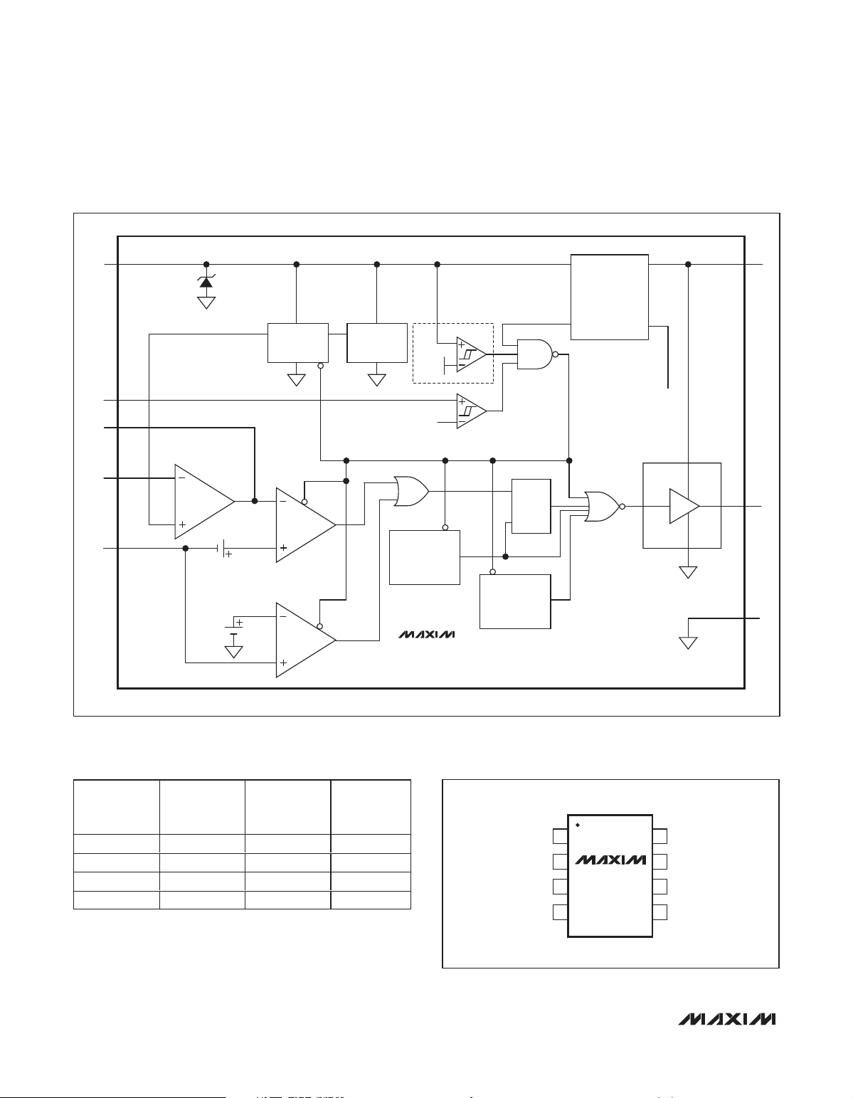
ᑍሆݛᒾዩᑺᔫ༽ౚăᏴᅲ߅Ⴥᎌೌᒄ༄Ljݙ
ገᄰ࢟Ꮞă
2* ᒇഗ࢟Ꮞ)1ᒗ41WৎLj2B*ೌᒗ,WJOHOEă
3* ࢟ኹܭာ݆MFEᑫ)ࠈቲೌLj861nBᑵሶ
࢟ഗሆኹଢ଼Ꮦᆐ23W*ೌᒗ,WMFE .WMFE࣡Ǘዴ
,WMFELjፓ.WMFEă
4* ᄰᄢሣK2K3ጲணᒏೡࣞࢯஂă
5* ࡌఎ࢟ᏎLj݀ၒྜྷ࢟ኹᐐଝࡵ21/9Wጲăၒ߲࢟ኹ
ᐐࡍࡵMFEᑫᑵሶມᒙ࢟ኹLj݀ᄋࡍᏖ 861nB
ᆮࢾࡼMFEຳ࢟ഗăၒྜྷ࢟ኹᐐᒗ 41WLjຳၒ߲
࢟ഗᏴᑳৈ࢟Ꮞ࢟ኹᆍดۣߒᆮࢾă
6* ࣥఎവK2Lj݀ᏴQXN`JOଝᏲQXNቧ)ຫൈᆐ
311I{-!ࣞᆐ1ᒗ3W*ă࠭1ᒗ211&খܤᐴహ܈LjMFE
ೡࣞႲᒄܤછLjሤ።࠭211&ܤછᒗ1&ăࡩ QXNቧ
ᐴహ܈ᆐ1&ဟLjMFEೡࣞᆐ 211&ă
7* ᄰK2݀ࣥఎK3ăೌጙৈభܤ࢟ኹᏎᒗMJO`JOLj
Ᏼ1ᒗ 2/7Wᒄମࢯஂ࢟ኹăMFEೡࣞᏴ211&Ꭷ1&ᒄ
ମܤછăၒྜྷMJO`JO࢟ኹᆐ 1WဟLjMFEೡࣞᆐ211&ă
வসǖݙঌᏲဟ༿ᇖຶৰۇ࢟ă
``````````````````````````````` ሮᇼႁී
NBY27913Cຶৰۇ)FW lju*ဵ࢟ഗ఼ᒜቯĂࡍ࢟ഗၒ߲
MFEདࣅLjభᄋࡉ861nB ࡼᆮࢾ࢟ഗLj༦ݙ၊࢟Ꮞ
࢟ኹܤછ፬ሰă
কຶৰۇ᎖ᔫᏴ373lI{Ăೌኚ࢟ഗෝါ)EDN*ࡼ
cvdl.cpptuᓞધLjඛৈᒲ໐ᆐၒ߲ᄋጙࢾถLjᄏࡼ
ถᒋᓍገན᎖࢟ঢઓభܠ߈ࡼᒋ࢟ঢ࢟ഗLjᎧ
ၒྜྷ࢟ኹᇄăږᑍᑚጙᒙLjຶৰۇࡼၒ߲࢟ኹᏴ
ࢾMFEᔫ࢟ኹሆ MFEࡼၒ߲࢟ഗᎧ࢟Ꮞ࢟ኹᇄă
কຶৰۇଐ᎖དࣅMFEঌᏲLj23W ᔫ࢟ኹሆభᄋ
ࡉ861nBࡼᔢࡍ࢟ഗăྙ MFEࡼᔫ࢟ኹ୷ࢅLjกඐ
ᔢࡍၒ߲࢟ഗږ܈ಿᐐଝLjభۣߒᆮࢾࡼၒ߲ൈă
ᆐདࣅݙᄴᔫ࢟ኹࡼMFEᑫLjኊገখܤଶഗ࢟ᔜăሆ
ෂ߲೫ݙᄴᔫ࢟ኹሆଶഗ࢟ᔜଐႯࡼሮᇼႁීă
ၒྜྷ࢟ᏎVWMP
ၒྜྷ࢟ᏎVWMP࢟വᎅ S4ĂS5ᔝ߅ࡼ࢟ᔜᆀဣሚăক
࢟ᔜᆀଶހၒྜྷ࢟Ꮞ࢟ኹLj݀Ᏼၒྜྷ࢟ኹ᎖21/9Wဟ
ᄰFO୭ࣅ࢟വăࡩ FO୭ࡼ࢟ኹဍဟLjታ
࢟ኹඡሢᆐ2/34WLjᎌ61nW ᒣૄăୈጙࡡఎဪᔫLj
ᒑᏴၒྜྷ࢟Ꮞ࢟ኹࢅ᎖21/5W )ఠࡵᒣૄ࢟ኹ*ဟݣ્
ࣥă
VWMPඡሢభږᑍሆါᄰ࢟ᔜS2 S3ቲࢯஂǖ
ᒦLjW
VWMP
ᆐჅገཇࡼVWMPඡሢăᆐۣߒඡሢறࣞLj
S5።ቃ᎖211lΩă
```````````````````````````````````````````````````````````````````````` Ꮔୈ።
ᓖǖᎧၤᏄୈ።ೊᇹဟLj༿ႁීิᑵᏴဧࡼဵNBY27913Că
V
⎛
R
UVLO
3
⎜
⎝
123
.
⎞
R
14=−
×
⎟
⎠
SUPPLIER PHONE FAX WEBSITE
Central Semiconductor 631-435-1110 631-435-3388 www.centralsemi.com
Coilcraft 847-639-6400 847-639-1469 www.coilcraft.com
Diodes Inc. 805-446-4800 805-446-4850 www.diodes.com
Murata 770-436-1300 770-436-3030 www.murata.com
Susumu Co Ltd. 208-328-0307 208-328-0308 www.susumu-usa.com
TDK 847-390-4373 847-390-4428 www.component.tdk.com
Vishay 402-563-6866 402-563-6296 www.vishay.com

ၒ߲ኹۣઐ
WMFEᑵ୭ሤ࣪᎖HOE ࡼᔢࡍ࢟ኹᎅS2ĂS3ᔝ߅ࡼ
ౣᆀሢᒜᏴ56WLjকᆀೌᒗNBY27913C ࡼGC
୭ăྙຶৰۇᏴᎌঌᏲဟఎMFEఎവLjᐌ
WMFEᑵ࢟ኹభถ્ဍࡵݙڔཝࡼ࢟ኹăดݝᇙތ
ࡍ્ଶހᑚᒬ༽ౚLj࠭ଢ଼ࢅ࢟ঢࡼᒋ࢟ഗLj
WMFEᑵ୭ࡼ࢟ኹሢᒜᏴ56W ጲดă૾ܣဧ೫ᑚᒬ
ۣઐLj྆ፇᏴຶৰۇ࢟ᒄ༄ᒎࢾࡼঌᏲă
QXNೡࣞࢯஂ
ᄰࢯஂೌᏴQXO`JOၒྜྷ࣡ࡼ QXNቧᐴహ܈఼
ᒜMFEೡࣞăQXN`JO ၒྜྷᆐ࢟ຳဟࣥMFE࢟ഗǗၒ
ྜྷᆐࢅ࢟ຳဟఎMFE࢟ഗăቧᒋᏴ 2/6Wᒗ6/1WĂຫ
ൈᆐ211I{ᒗ 2111I{Ljᄰখܤᐴహ܈ࢯஂMFEೡࣞăຫ
ൈࢅ᎖211I{ࡼቧభถ્ࡴᒘၒ߲࿑ႄăᐐࡍᐴహ܈ဟLj
MFEೡࣞିྦྷLjᒄጾăQXNᐴహ܈ᆐ 1&ဟLjMFEೡ
ࣞࡉࡵ211&ă
ሣቶೡࣞࢯஂ
ሣቶೡࣞࢯஂဵᄰখܤMJO`JOၒྜྷ࢟ኹࡼ఼ࣞᒜ
MFEೡࣞăMJO`JOၒྜྷࢯᒜଶഗቧLjᏴݙᄴࡼ࢟ഗሆ
߿NPTGFUăᑚጙ߈્ጙݛ఼ᒜၒ߲࢟ഗLj࠭ࡉ
ࡵ఼ᒜMFEೡࣞࡼࡼăፐᆐᏴྀೡࣞࢀ MFEဪᒫۣ
ߒࡴᄰᓨზLjሣቶೡࣞࢯஂݙ્ޘည࿑ႄሚሷăᏴ1ᒗ
2/7WᆍดࢯஂMJO`JO ࢟ኹLjభဧMFEೡࣞᏴ211&ᒗ1&
ମܤછăMJO`JO࢟ኹᐐࡍဟLjMFEೡࣞିྦྷLjᒄጾă
MJO`JO࢟ኹᆐ1W ဟLjMFEೡࣞᆐ211&ă
ࢯஂၒ߲ൈ
োሆါࢯஂଶഗ࢟ᔜS:Ljభጲখܤຶৰۇࡼᔢࡍ
ၒ߲ൈǖ23WĂ861nBăᓖፀǖຶৰۇᔢࡍၒ߲࢟ഗሢ
ᒜᏴ861nBĂᔢࡍၒ߲࢟ኹሢᒜᏴ26WLj༦ᔢࡍၒ߲ൈ
ሢᒜᏴ9/36Xă
၅ሌଐႯᔢቃၒྜྷ࢟ኹሆࡼᔢଛࡴᄰᐴహ܈ǖ
ᒦLjW
JONJO
ᆐᔢቃၒྜྷ࢟ኹLjW
MFE
ᆐMFEᔫ࢟ኹLj
J
MFE
ᆐჅገཇࡼMFE࢟ഗLjWEᆐE3ࡼᑵሶ࢟ኹă
ଐႯჅገཇࡼᒋ࢟ঢ࢟ഗǖ
ᒦLjl
g
ᆐĐኀᑵፐᔇđ)ஏᇹၫ*Ljক࢟വᒦ
ᒙᆐ2/2ă
ଐႯჅኊࡼ࢟ঢᒋLj݀ኡᐋᔢதܪᓰᒋࡣቃ᎖ଐႯᒋ
ࡼ࢟ঢǖ
ᒦLjMᆐ࢟ঢM2ࡼ࢟ঢᒋǗgTXᆐఎຫൈLjࢀ᎖373lI{ă
ᄰ૮ෝါᄋၒ߲࢟വࡼൈᆐǖ
ၒ߲࢟വሿࡼൈᆐǖ
োถ၆ࢾേLjၤೝৈࢀါሤࢀLj࠭ཇ߲ጙৈ
ৎறཀྵࡼᒋ࢟ঢ࢟ഗǖ
োཇࡻࡼJ
QFBL
LjಽሆါଐႯଶഗ࢟ᔜS:ǖ
ᒦLj1/3:3Wᆐଶഗඡሢ࢟ኹăS8ĂS9ᔝ߅ጙৈ࢟ᔜ
ኹLjถ৫Ᏼୈଶഗ୭ᒄ༄ږ܈ಿଢ଼ࢅଶഗ࢟ᔜ
ࡼኹଢ଼ă
ᄢሣኡᐋ
ݙဧQXNೡࣞࢯஂဟᄢሣ K2ᄰǗݙဧሣቶೡࣞ
ࢯஂဟᄢሣK3ᄰă
ຶৰۇǖNBY27913C
NBY27913Cຶৰۇ
_______________________________________________________________________________________ 3
VV
+
D
=
ON
LED D
VVV
++
INMIN LED D
kI
××
f LED
I
=
P
D
−21
ON
DV
×
ON INMIN
L
=
fI
×
SW P
1
PLIf
=×× ×
IN P SW
2
2
PVIVI
=×+×
OUT LED LED D LED
×+×
⎛
2( )VVI
IP=
R
LED D LED
⎜
⎝
0 292 8 7
.( )
9
=
×
fL
SW
RR
×+
IR
×
PEAK
7
⎞
⎟
⎠
ຶৰۇǖNBY27913C
NBY27913Cຶৰۇ
4 _______________________________________________________________________________________
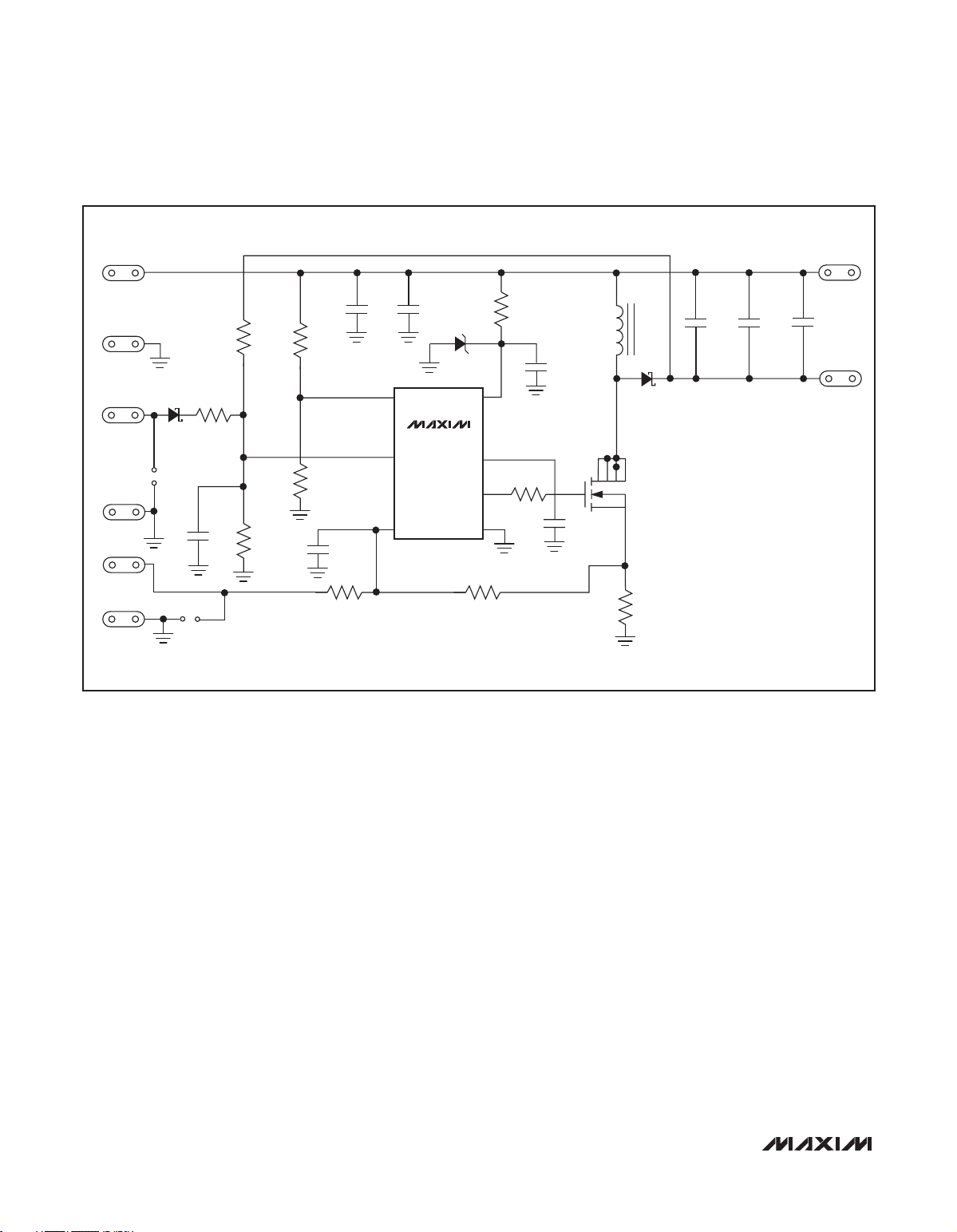
ᅄ2/! NBY27913CຶৰۇᏇಯᅄ
+VIN
1%
R1
392kΩ
1%
R5
C9
R2
1nF
11kΩ
50V
1%
GND
D3
SD103CWS
J2
1kΩ
PWM_IN
J1
PWM_GND
LIN_IN
LIN_GND
R3
499kΩ
1%
R4
73.2kΩ
1%
C8
470pF
50V
R7
1kΩ
1%
C1
4.7μF
50V
1
2
3
4
UVLO/EN
MAX16802B
DIM/FB
COMP
CS
C2
4.7μF
50V
-VLED
R6
330Ω
D1
1%
22V
C3
0.1μF
R10
1Ω
50V
3
C7
0.1μF
50V
8
IN
U1
7
V
CC
6
NDRV
5
GND
R8
220Ω
1%
12
56
L1
4.7μH
CMSH1-60M
Q1
Si3458DV
4
R9
0.10Ω
1%
C4
0.1μF
50V
D2
C5
4.7μF
50V
C6
4.7μF
50V
+VLED

ຶৰۇǖNBY27913C
NBY27913Cຶৰۇ
ᅄ3/! NBY27913CຶৰۇᏄୈݚ—Ꮔୈށ ᅄ4/! NBY27913CຶৰۇQDCݚ—Ꮔୈށ
ᅄ5/! NBY27913CຶৰۇQDCݚ—ށ
Nbyjnݙ࣪ Nbyjnޘອጲᅪࡼྀ࢟വဧঌᐊLjጐݙᄋᓜಽభăNbyjnۣഔᏴྀဟମĂᎌྀᄰۨࡼ༄ᄋሆኀখޘອᓾ೯ৃࡼཚಽă
Maxim Integrated Products, 120 San Gabriel Drive, Sunnyvale, CA 94086 408-737-7600 ______________________5
© 2006 Maxim Integrated Products Printed USA
ဵ
Nbyjn!Joufhsbufe!Qspevdut-!Jod/
ࡼᓖݿܪă

MAX16802BEVKIT MAX16802B评估板 - 概述
ENGLISH • 简体中文 • 日本語 • 한국어
Login | Register
请输入关键词或器件型号
最新内容 产品 方案 设计 应用 技术支持 销售联络 公司简介 我的Maxim
Maxim > 产品 > 电源和电池管理 > MAX16802BEVKIT
MAX16802BEVKIT
MAX16802B评估板
概述 技术文档 定购信息 用户说明 (0) 所有内容
状况
状况:生产中。
概述
MAX16802B评估板(EV kit) 用来演示基于MAX16802B的电流控制型、大电
流LED驱动器。该评估板具备高达750mA的稳定电流供给能力,并可运行
在10.8V至30V电源电压之间,工作温度范围为-40°C至+85°C。
MAX16802B评估板具有两种不同类型的亮度控制方式:使用模拟输入电压
或PWM输入信号来控制LED亮度。该评估板还具有UVLO功能,可以在输入电源
电压过低时关闭评估板,并且可以在LED开路时为评估板提供过压保
护。MAX16802B评估板是一块经过完全安装与测试的电路板。
完整的数据资料
英文
中文
下载
下载
Rev. 0 (PDF, 132kB)
Rev. 0 (PDF, 640kB)
警告:当出现严重故障或失效状态时,本评估板有巨大能量耗散,可能会造成元件或元件碎片的高速溅射。请小心操作本
评估板,以避免可能的人身伤害。
关键特性 应用/使用
10.8V至30V电源电压范围
电流控制型输出
12V输出时,电流可高达750mA
线性或PWM亮度控制
满载时效率高达80%
商用与工业照明
装饰灯与建筑照明
离线式DC- DC LED驱动器
RGB背光,用于LCD TV和监视
器
电源电压欠压锁定
输出过压保护
相关产品
MAX16801,
离线式、DC- DC PWM 控制器,用于高亮度LED驱动器
MAX16801A,
MAX16801B,
MAX16802,
MAX16802A,
MAX16802B
没有找到你需要的产品吗?
应用工程师帮助选型,下个工作日回复
参数搜索
应用帮助
概述 技术文档 定购信息
概述 数据资料 价格与供货
http://china.maxim-ic.com/datasheet/index.mvp/id/5209[2010-8-12 8:16:14]

MAX16802BEVKIT MAX16802B评估板 - 概述
关键特性
应用/使用
关键指标
图表
注释、注解
相关产品
联络我们:信息反馈、提出问题 • 对该网页的评价 • 发送本网页 • 隐私权政策 • 法律声明
© 2010 Maxim Integrated Products 版权所有
应用笔记
评估板
设计指南
可靠性报告
软件/模型
参考文献: 19-0560 Rev. 0; 2006-05-30
本页最后一次更新: 2006-07-20
样品
在线订购
封装信息
无铅信息
http://china.maxim-ic.com/datasheet/index.mvp/id/5209[2010-8-12 8:16:14]

General Description
The MAX16802B evaluation kit (EV kit) demonstrates a
current-controlled, high-output-current LED driver
based on the MAX16802B. This EV kit is capable of
supplying stable output currents of up to 750mA, can
run at supply voltages between 10.8V and 30V, and can
operate at temperatures ranging from -40°C to +85°C.
The MAX16802B EV kit features two different types of
dimming controls using either a linear input voltage or a
PWM input signal to control the LED brightness. This EV
kit also has a UVLO feature to turn off the EV kit operation during low input supply voltage and an overvoltage
protection to protect the EV kit under an open-LED condition. The MAX16802B EV kit is a fully assembled and
tested board.
Warning: Under severe fault or failure conditions, this
EV kit may dissipate large amounts of power, which
could result in the mechanical ejection of a component
or of component debris at high velocity. Operate this
EV kit with care to avoid possible personal injury.
Features
♦ 10.8V to 30V Wide Supply Voltage Range
♦ Current-Controlled Output
♦ Up to 750mA LED Current at 12V Output
♦ Linear and PWM Dimming Control
♦ Over 80% Efficiency at Full Load
♦ Supply Undervoltage Lockout
♦ Output Overvoltage Protection
Evaluates: MAX16802B
MAX16802B Evaluation Kit
________________________________________________________________ Maxim Integrated Products 1
19-0560; Rev 0; 5/06
Component List
For pricing, delivery, and ordering information, please contact Maxim/Dallas Direct! at
1-888-629-4642, or visit Maxim’s website at www.maxim-ic.com.
Ordering Information
µMAX is a registered trademark of Maxim Integrated Products, Inc.
DESIGNATION QTY DESCRIPTION
C1, C2, C5, C6 4
C3, C4, C7 3
C8 1
C9 1
D1 1
D2 1
D3 1
J1, J2 2
4.7µF, 50V X7R ceramic capacitors
Murata GRM32ER71H475KA88L
0.1µF, 50V X7R SMD ceramic
capacitors
Murata GRM188R71H104KA93D or
TDK C1608X7R1H104K
470pF, 50V X7R ceramic capacitor
Murata GRM188R71H471KA01D or
TDK C1608X7R1H471K
1nF, 50V X7R ceramic capacitor
Murata GRM188R71H102KA01D or
TDK C1608X7R1H102K
22V, 1.5W zener diode
Vishay SMZG3797B
60V, 1A Schottky diode
Central Semiconductor CMSH1-60M
or Diodes Inc. B160
20V, small-signal Schottky diode
Vishay SD103CWS or
Diodes Inc. SD103CWS
0.1in, 2-pin hole headers
(through hole)
PART TEMP RANGE IC PACKAGE
MAX16802BEVKIT -40°C to +85°C 8 µMAX
®
DESIGNATION QTY DESCRIPTION
L1 1
Q1 1
R1 1 392kΩ ±1%, 1/8W resistor (0603)
R2 1 11kΩ ±1%, 1/8W resistor (0603)
R3 1 499kΩ ±1%, 1/8W resistor (0603)
R4 1 73.2kΩ ±1%, 1/8W resistor (0603)
R5, R7 2 1kΩ ±1%, 1/8W resistors (0603)
R6 1 330Ω ±1%, 1/4W resistor (1206)
R8 1 220Ω ±1%, 1/8W resistor (0603)
R9 1
R10 1 1Ω ±5%, 1/8W resistor (0603)
U1 1 MAX16802B (8-pin µMAX)
VIN, VLED,
PWM_IN,
LIN_IN
— 1 MAX16802B PC board
4.7µH, 4.2A peak SMD inductor
Coilcraft DO3308P-472ML
60V, 3.2A n-channel MOSFET
Vishay Si3458DV
0.10Ω ±1%, 1/2W resistor (1206)
Susumu RL1632R-R100-F
0.1in, 2-pin male connectors
4
(through hole)

Evaluates: MAX16802B
MAX16802B Evaluation Kit
2 _______________________________________________________________________________________
Quick Start
The MAX16802B EV kit is fully assembled and tested.
Follow these steps to verify operation. Do not turn on
the power supply until all connections are completed.
1) Connect a DC power supply (0 to 30V or above, 1A)
to +VIN and GND.
2) Connect a voltmeter or oscilloscope and the LED
array (connected in series to drop about 12V at
750mA forward current) to +VLED and -VLED with
anode connected to +VLED and cathode to -VLED.
3) Close the jumpers J1 and J2 to disable dimming.
4) Turn on the power supply and increase the input
voltage to above 10.8V. The output voltage increases to forward bias the LED array and delivers
approximately 750mA regulated average LED current. Increase the supply further up to 30V and the
output average current will be regulated throughout
the range.
5) Open shunt J1 and apply a PWM signal to PWM_IN
with a frequency of 200Hz and 0 to 2V amplitude.
Vary the duty cycle from 0 to 100% and the LED
brightness varies from 100% to 0%. When the PWM
duty cycle is 0%, the LED brightness is 100%.
6) Close J1, and then open J2. Connect a variable voltage source to LIN_IN and vary the voltage between
0 and 1.6V. The LED brightness varies from 100% to
0%. When the voltage input at LIN_IN is 0V, the LED
brightness is 100%.
Caution: Avoid powering up the EV kit without connecting load.
Detailed Description
The MAX16802B evaluation kit is a current-controlled,
high-output-current LED driver capable of supplying
constant currents up to 750mA, irrespective of supply
voltage variations.
This EV kit is based on a discontinuous current mode
(DCM) buck-boost converter operating at 262kHz to
deliver a finite amount of energy to the output every
cycle. The amount of this energy depends primarily on
the value of the inductor and the user-programmable
peak inductor current and does not depend on the supply voltage. Due to this configuration, the power output
of the EV kit, and thus the output current supplied to the
LED at a given LED operating voltage, becomes independent of the supply voltage.
This EV kit is designed to drive LED loads capable of
taking up to 750mA of maximum current at a 12V operating voltage. If an LED load with lower operating voltage
is used, then the maximum output current will increase
by the same ratio to maintain the output power constant.
To drive an LED array with a different operating voltage,
the value of the current-sense resistor needs to be
adjusted. Calculation of the current-sense resistor for a
different output operating voltage is explained in later
sections.
Input Supply UVLO
Input supply UVLO is implemented by using a resistor
network that combines R3 and R4, which senses the
input supply voltage and uses the EN pin to turn on the
circuit when the input supply voltage goes above
10.8V. The wake-up threshold of EN is 1.23V when the
voltage at EN is rising, and it has a hysteresis of 50mV.
Once the device is turned on, due to the hysteresis, the
device turns off only if the input supply voltage goes
below 10.4V.
The UVLO threshold can be adjusted by varying R1 or
R2 using the equation below:
where V
UVLO
is the desired UVLO threshold. To main-
tain threshold accuracy, keep the value of R4 less than
100kΩ.
Component Suppliers
Note: Indicate you are using the MAX16802B when contacting these manufacturers.
V
⎛
R
UVLO
3
⎜
⎝
123
.
⎞
R
14=−
×
⎟
⎠
SUPPLIER PHONE FAX WEBSITE
Central Semiconductor 631-435-1110 631-435-3388 www.centralsemi.com
Coilcraft 847-639-6400 847-639-1469 www.coilcraft.com
Diodes Inc. 805-446-4800 805-446-4850 www.diodes.com
Murata 770-436-1300 770-436-3030 www.murata.com
Susumu Co Ltd. 208-328-0307 208-328-0308 www.susumu-usa.com
TDK 847-390-4373 847-390-4428 www.component.tdk.com
Vishay 402-563-6866 402-563-6296 www.vishay.com

Output Overvoltage Protection
The maximum voltage at the positive pin of VLED with
respect to GND is limited to 45V by a feedback network
formed by R1 and R2, which is connected to the FB pin
of the MAX16802B. If the EV kit is turned on with no load
or if the LED connection opens, the voltage at the positive pin of VLED may rise to unsafe levels. This condition
is sensed by the internal error amplifier, which reduces
the peak inductor current to limit the voltage at the positive pin of VLED to 45V. Even if this protection is present,
it is recommended to connect the specified load before
powering up the EV kit.
PWM Dimming
The PWM dimming is for controlling the LED brightness
by adjusting the duty cycle of the PWM input signal
connected to the PWM_IN input. A HIGH at PWM_IN
input turns off the LED current and LOW turns on the
LED current. Connect a signal with peak amplitude
between 1.5V to 5.0V and with frequency between
100Hz to 1000Hz and vary the duty cycle to adjust the
LED brightness. Frequencies lower than 100Hz can
introduce flickering in the light output. LED brightness
reduces when duty cycle is increased and vice-versa.
When the PWM duty cycle is 0%, the LED brightness
will be 100%.
Linear Dimming
The linear dimming is for controlling the LED brightness
by varying the amplitude of the voltage connected to
the LIN_IN input. The voltage at the LIN_IN input modulates the current-sense signal and makes the MOSFET
trip at a different current level. This process, in turn,
changes the output current and thus controls the LED
brightness. Since the LED is continuously on at all
brightness levels, flickering effect is not present with
linear dimming. Vary the LIN_IN voltage between 0 and
1.6V to adjust LED brightness from 100% to 0%. LED
brightness reduces when the voltage at LIN_IN is
increased and vice-versa. When the voltage at LIN_IN
is 0V the LED brightness is 100%.
Adjusting the Output Power
To change the maximum output power of the EV kit
from 12V at 750mA to a different level, adjust the value
of the current-sense resistor, R9, using the following
equations. Note that the maximum output current of the
EV kit is limited to 750mA, the maximum output voltage
is limited to 15V, and the maximum output power is limited to 8.25W.
Initially calculate the approximate optimum ON duty
cycle required at the minimum input voltage:
where V
INMIN
is the minimum input supply voltage,
V
LED
is the LED operating voltage, I
LED
is the desired
LED current and VDis the forward voltage of D2.
Calculate the approximate required peak inductor current:
where kfis a noncritical “fudge factor” set equal to 1.1
for this circuit.
Calculate the approximate required inductor value and
choose the closest standard value smaller than the calculated value:
where L is the inductance value of inductor L1, and f
SW
is the switching frequency equal to 262kHz.
Power transferred to the output circuit by the flyback
process is:
Power consumed by the output circuit is:
Conservation of power requires that the above two
equations can be equated and solved for a more precise value of the required peak inductor current.
Set the value of the current-sense resistor, R9, based
on the I
PEAK
value using the following equation:
where 0.292V is the current-sense trip threshold voltage. R7 and R8 form a voltage-divider, which scales
down the voltage across the current-sense resistor
before reaching the current-sense pin of the device.
Jumper Selection
Keep jumper J1 closed when PWM dimming is not
used. Keep jumper J2 closed when linear dimming is
not used.
Evaluates: MAX16802B
MAX16802B Evaluation Kit
_______________________________________________________________________________________ 3
VV
+
D
=
ON
LED D
VVV
++
INMIN LED D
kI
××
f LED
I
=
P
D
−21
ON
DV
×
ON INMIN
L
=
fI
×
SW P
1
PLIf
=×× ×
IN P SW
2
2
PVIVI
=×+×
OUT LED LED D LED
×+×
⎛
2( )VVI
IP=
LED D LED
⎜
⎝
×
fL
SW
⎞
⎟
⎠
0 292 8 7
R
9
=
RR
×+
.( )
IR
PEAK
7
×

Evaluates: MAX16802B
MAX16802B Evaluation Kit
4 _______________________________________________________________________________________
Figure 1. MAX16802B EV Kit Schematic
+VIN
1
2
3
4
UVLO/EN
MAX16802B
DIM/FB
COMP
CS
C2
4.7µF
50V
C1
4.7µF
C8
470pF
50V
R7
1kΩ
1%
50V
R5
1%
C9
1nF
50V
R1
392kΩ
1%
R2
11kΩ
1%
GND
D3
SD103CWS
J2
1kΩ
PWM_IN
J1
PWM_GND
LIN_IN
LIN_GND
R3
499kΩ
1%
R4
73.2kΩ
1%
-VLED
R6
330Ω
D1
1%
22V
C3
0.1µF
R10
1Ω
50V
3
C7
0.1µF
50V
8
IN
U1
7
V
CC
6
NDRV
5
GND
R8
220Ω
1%
12
56
L1
4.7µH
CMSH1-60M
Q1
Si3458DV
4
R9
0.10Ω
1%
C4
0.1µF
50V
D2
C5
4.7µF
50V
C6
4.7µF
50V
+VLED

Maxim cannot assume responsibility for use of any circuitry other than circuitry entirely embodied in a Maxim product. No circuit patent licenses are
implied. Maxim reserves the right to change the circuitry and specifications without notice at any time.
Maxim Integrated Products, 120 San Gabriel Drive, Sunnyvale, CA 94086 408-737-7600 _____________________ 5
© 2006 Maxim Integrated Products Printed USA is a registered trademark of Maxim Integrated Products, Inc.
Evaluates: MAX16802B
MAX16802B Evaluation Kit
Boblet
Figure 2. MAX16802B EV Kit Component Placement Guide—
Component Side
Figure 3. MAX16802B EV Kit PC Board Layout—Component
Side
Figure 4. MAX16802B EV Kit PC Board Layout—Solder Side

For pricing, delivery, and ordering information, please contact Maxim Direct at 1-888-629-4642,
or visit Maxim’s website at www.maxim-ic.com.
General Description
The MAX16801A/B/MAX16802A/B high-brightness (HB)
LED driver-control ICs contain all the circuitry required
for the design of wide-input-voltage-range LED drivers
for general lighting and display applications. The
MAX16801 is well suited for universal input (rectified
85VAC to 265VAC) LED drivers, while the MAX16802 is
intended for low-input-voltage (10.8VDC to 24VDC) LED
drivers.
When the LED current needs to be tightly regulated, an
additional on-board error amplifier with 1% accurate reference can be utilized. A wide dimming range can be
implemented by using low-frequency PWM dimming.
The MAX16801/MAX16802 feature an input undervoltage
lockout (UVLO) for programming the input-supply start
voltage, and to ensure proper operation during brownout
conditions. The MAX16801 has an internal-bootstrap
undervoltage lockout circuit with a large hysteresis that
simplifies offline LED driver designs. The MAX16802 does
not have this internal bootstrap circuit and can be biased
directly from a +12V rail.
The 262kHz fixed switching frequency is internally
trimmed, allowing for optimization of the magnetic and filter components, resulting in a compact, cost-effective
LED driver. The MAX16801A/MAX16802A are offered with
50% maximum duty cycle. The MAX16801B/MAX16802B
are offered with 75% maximum duty cycle. These devices
are available in an 8-pin µMAX
®
package and operate
over the -40°C to +85°C temperature range.
Applications
Features
♦ Suitable for Buck, Boost, Flyback, SEPIC, and
Other Topologies
♦ Up to 50W or Higher Output Power
♦ Universal Offline Input Voltage Range: Rectified
85VAC to 265VAC (MAX16801)
♦ IN Pin Directly Driven From 10.8VDC to 24VDC
Input (MAX16802)
♦ Internal Error Amplifier with 1% Accurate
Reference for Precise LED Current Regulation
♦ PWM or Linear Dimming
♦ Fixed Switching Frequency of 262kHz ±12%
♦ Thermal Shutdown
♦ Digital Soft-Start
♦ Programmable Input Startup Voltage
♦ Internal Bootstrap UVLO with Large Hysteresis
(MAX16801)
♦ 45µA (typ) Startup Supply Current, 1.4mA (typ)
Operating Supply Current
♦ 50% (MAX16801A/MAX16802A) or 75%
(MAX16801B/MAX16802B) Maximum Duty Cycle
♦ Available in a Tiny 8-Pin µMAX Package
MAX16801A/B/MAX16802A/B
Offline and DC-DC PWM Controllers for
High-Brightness LED Drivers
________________________________________________________________ Maxim Integrated Products 1
Ordering Information
19-3880; Rev 2; 1/10
PART
TEMP
RANGE
PINPACKAGE
MAX16801AEUA+ -40°C to +85°C 8 µMAX
MAX16801BEUA+ -40°C to +85°C 8 µMAX
MAX16802AEUA+ -40°C to +85°C 8 µMAX
MAX16802BEUA+ -40°C to +85°C 8 µMAX
+Denotes lead-free package.
Offline and DC-DC LED
Drivers
RGB Back Light for LCD
TVs and Monitors
Commercial and
Industrial Lighting
Decorative and
Architectural Lighting
EVALUATION KIT
AVAILABLE
Q1
MAX16802B
10.8VDC TO 24VDC
PWM
GND
C1 R1
L1
D1
C2
C3
LEDs
CS
COMP
DIM/FB
UVLO/EN IN
V
CC
NDRV
GND
ENABLE
Typical Operating Circuit
Warning: The MAX16801/MAX16802 are designed to work with high voltages. Exercise caution.
µMAX is a registered trademark of Maxim Integrated Products, Inc.

MAX16801A/B/MAX16802A/B
Offline and DC-DC PWM Controllers for
High-Brightness LED Drivers
2 _______________________________________________________________________________________
ABSOLUTE MAXIMUM RATINGS
ELECTRICAL CHARACTERISTICS
(VIN= +12V (MAX16801: VINmust first be brought up to +23.6V for startup), 10nF bypass capacitors at IN and VCC, C
NDRV
= 0µF,
V
UVLO
= +1.4V, V
DIM/FB
= +1.0V, COMP = unconnected, VCS= 0V, TA= -40°C to +85°C, unless otherwise noted. Typical values are
at T
A
= +25°C.) (Note 1)
Stresses beyond those listed under “Absolute Maximum Ratings” may cause permanent damage to the device. These are stress ratings only, and functional
operation of the device at these or any other conditions beyond those indicated in the operational sections of the specifications is not implied. Exposure to
absolute maximum rating conditions for extended periods may affect device reliability.
IN to GND
..........................................................................
-0.3V to +30V
V
CC
to GND
......................................................................
-0.3V to +13V
DIM/FB, COMP, UVLO, CS to GND..........................-0.3V to +6V
NDRV to GND.............................................-0.3V to (V
CC
+ 0.3V)
Continuous Power Dissipation (TA = +70°C)
8-Pin µMAX (derate 4.5mW/°C above +70°C) ..............362mW
Operating Temperature Range ...........................-40°C to +85°C
Storage Temperature Range ............................-65°C to +150°C
Junction Temperature......................................................+150°C
Lead Temperature (soldering, 10s) .................................+300°C
PARAMETER
CONDITIONS
UNDERVOLTAGE LOCKOUT/STARTUP
Bootstrap UVLO Wake-Up Level
V
SUVR
VIN rising (MAX16801 only)
V
Bootstrap UVLO Shutdown Level
V
SUVF
VIN falling (MAX16801 only)
V
UVLO/EN Wake-Up Threshold V
ULR2
UVLO/EN rising
V
UVLO/EN Shutdown Threshold V
ULF2
UVLO/EN falling
V
UVLO/EN Input Current I
UVLO
TJ = +125°C 25 nA
UVLO/EN Hysteresis 50 mV
IN Supply Current In
Undervoltage Lockout
I
START
VIN = +19V, for MAX16801 only when in
bootstrap UVLO
45 90 µA
IN Voltage Range V
IN
24 V
t
EXTR
UVLO/EN steps up from +1.1V to +1.4V 12
UVLO/EN Propagation Delay
t
EXTF
UVLO/EN steps down from +1.4V to +1.1V 1.8
µs
t
BUVR
VIN steps up from +9V to +24V 5
Bootstrap UVLO Propagation
Delay
t
BUVF
VIN steps down from +24V to +9V 1
µs
INTERNAL SUPPLY
VCC Regulator Set Point V
CCSP
VIN = +10.8V to +24V, sinking 1µA to 20mA
from V
CC
7
V
IN Supply Current After Startup I
IN
VIN = +24V 1.4 2.5 mA
Shutdown Supply Current UVLO/EN = low 90 µA
GATE DRIVER
)
Measured at NDRV sinking, 100mA 2 4
Driver Output Impedance
)
Measured at NDRV sourcing, 20mA 4 12
Ω
Driver Peak Sink Current 1A
Driver Peak Source Current
A
PWM COMPARATOR
Comparator Offset Voltage
V
COMP
- V
CS
V
CS Input Bias Current I
CS
VCS = 0V -2 +2 µA
Comparator Propagation Delay t
PWM
VCS = +0.1V 60 ns
Minimum On-Time
)
ns
SYMBOL
MIN TYP MAX UNITS
19.68 21.6 23.60
9.05 9.74 10.43
1.188 1.28 1.371
1.168 1.23 1.291
10.8
R
ON(LOW
R
ON(HIGH
VO
PWM
1.15 1.38 1.70
t
ON(MIN
0.65
150
10.5

MAX16801A/B/MAX16802A/B
Offline and DC-DC PWM Controllers for
High-Brightness LED Drivers
_______________________________________________________________________________________ 3
Note 1: All devices are 100% tested at TA= +85°C. All limits over temperature are guaranteed by characterization.
Note 2: V
REF
is measured with DIM/FB connected to the COMP pin (see the Functional Diagram).
Note 3: The MAX16801 is intended for use in universal input offline drivers. The internal clamp circuit is used to prevent the boot-
strap capacitor (C1 in Figure 5) from charging to a voltage beyond the absolute maximum rating of the device when
EN/UVLO is low. The maximum current to IN (hence to clamp) when UVLO is low (device in shutdown), must be externally
limited to 2mA (max). Clamp currents higher than 2mA may result in clamp voltage higher than +30V, thus exceeding the
absolute maximum rating for IN. For the MAX16802, do not exceed the +24V maximum operating voltage of the device.
ELECTRICAL CHARACTERISTICS (continued)
(VIN= +12V (MAX16801: VINmust first be brought up to +23.6V for startup), 10nF bypass capacitors at IN and VCC, C
NDRV
= 0µF,
V
UVLO
= +1.4V, V
DIM/FB
= +1.0V, COMP = unconnected, VCS= 0V, TA= -40°C to +85°C, unless otherwise noted. Typical values are
at T
A
= +25°C.) (Note 1)
PARAMETER
CONDITIONS
CURRENT-SENSE COMPARATOR
Current-Sense Trip Threshold V
CS
320 mV
CS Input Bias Current I
CS
VCS = 0V -2 +2 µA
Propagation Delay From
Comparator Input to NDRV
t
PWM
50mV overdrive 60 ns
Switching Frequency f
SW
290 kHz
MAX1680_A 50
Maximum Duty Cycle D
MAX
MAX1680_B 75 76
%
IN CLAMP VOLTAGE
IN Clamp Voltage V
INC
2mA sink current, MAX16801 only (Note 3)
V
ERROR AMPLIFIER
Voltage Gain R
LOAD
= 100kΩ 80 dB
Unity-Gain Bandwidth R
LOAD
= 100kΩ, C
LOAD
= 200pF 2
Phase Margin R
LOAD
= 100kΩ, C
LOAD
= 200pF 65
DIM/FB Input Offset Voltage 3mV
High 2.2 3.5
COMP Clamp Voltage
Low 0.4 1.1
V
Source Current 0.5 mA
Sink Current 0.5 mA
Reference Voltage V
REF
(Note 2)
V
Input Bias Current 50 nA
COMP Short-Circuit Current 8mA
THERMAL SHUTDOWN
Thermal-Shutdown Temperature
°C
Thermal Hysteresis 25 °C
DIGITAL SOFT-START
Soft-Start Duration
Clock
Reference Voltage Steps During
Soft-Start
31
Reference Voltage Step 40 mV
SYMBOL
MIN TYP MAX UNITS
262 291
230 262
24.1 26.1 29.0
1.218 1.230 1.242
130
15,872
50.5
MHz
D eg r ees
cycles
Steps

MAX16801A/B/MAX16802A/B
Offline and DC-DC PWM Controllers for
High-Brightness LED Drivers
4 _______________________________________________________________________________________
Typical Operating Characteristics
(V
UVLO/EN
= +1.4V, VFB= +1V, COMP = unconnected, VCS= 0V, TA= +25°C, unless otherwise noted.)
BOOTSTRAP UVLO WAKE-UP LEVEL
vs. TEMPERATURE
MAX16801 toc01
TEMPERATURE (°C)
V
IN
(V)
6040200-20
21.35
21.40
21.45
21.50
21.55
21.60
21.30
-40 80
MAX16801 VIN RISING
BOOTSTRAP UVLO SHUTDOWN LEVEL
vs. TEMPERATURE
MAX16801 toc02
TEMPERATURE (°C)
V
IN
(V)
6040200-20
9.8
9.9
10.0
10.1
9.7
-40 80
MAX16801 VIN FALLING
UVLO/EN WAKE-UP THRESHOLD
vs. TEMPERATURE
MAX16801 toc03
TEMPERATURE (°C)
UVLO/EN (V)
6040200-20
1.255
1.260
1.265
1.270
1.275
1.280
1.250
-40 80
UVLO/EN RISING
UVLO/EN SHUTDOWN THRESHOLD
vs. TEMPERATURE
MAX16801 toc04
TEMPERATURE (°C)
UVLO/EN (V)
6040200-20
1.15
1.20
1.25
1.30
1.10
-40 80
UVLO/EN FALLING
VIN SUPPLY CURRENT IN UNDERVOLTAGE
LOCKOUT vs. TEMPERATURE
MAX16801 toc05
TEMPERATURE (°C)
I
START
(µA)
6040200-20
43
44
45
46
47
48
49
50
51
52
42
-40 80
VIN = 19V
MAX16801 WHEN IN BOOTSTRAP UVLO
MAX16802 WHEN UVLO/EN IS LOW
VIN SUPPLY CURRENT AFTER STARTUP
vs. TEMPERATURE
MAX16801 toc06
TEMPERATURE (°C)
I
IN
(mA)
6040200-20
1.2
1.3
1.4
1.5
1.1
-40 80
VIN = 24V
VCC REGULATOR SET POINT
vs. TEMPERATURE
MAX16801 toc07
TEMPERATURE (°C)
V
CC
(V)
6040200-20
9.3
9.5
9.4
9.7
9.6
9.8
9.2
-40 80
VIN = 19V
NO LOAD
NDRV OUTPUT IS NOT
SWITCHING, V
FB
= 1.5V
NDRV OUTPUT IS
SWITCHING
VCC REGULATOR SET POINT
vs. TEMPERATURE
MAX116801 toc08
TEMPERATURE (°C)
V
CC
(V)
6040200-20
8.2
8.5
8.6
8.4
8.3
8.8
8.7
8.9
8.1
-40 80
VIN = 10.8V
10mA LOAD
20mA LOAD
CURRENT-SENSE THRESHOLD
vs. TEMPERATURE
MAX16801 toc09
TEMPERATURE (°C)
CURRENT-SENSE THRESHOLD (µV)
6040200-20
275
290
295
285
280
305
300
310
270
-40 80
+3σ
-3σ
MEAN
TOTAL NUMBER OF
DEVICES = 100

MAX16801A/B/MAX16802A/B
Offline and DC-DC PWM Controllers for
High-Brightness LED Drivers
_______________________________________________________________________________________ 5
CURRENT-SENSE THRESHOLD
MAX16801 toc10
CURRENT-SENSE THRESHOLD (mV)
PERCENTAGE OF UNITS (%)
310300290280270
5
10
15
20
25
30
0
260 320
TOTAL NUMBER OF
DEVICES = 200
SWITCHING FREQUENCY
vs. TEMPERATURE
MAX16801 toc11
TEMPERATURE (°C)
SWITCHING FREQUENCY (kHz)
6040200-20
245
260
265
255
250
275
270
280
240
-40 80
+3σ
-3σ
MEAN
TOTAL NUMBER OF
DEVICES = 100
SWITCHING FREQUENCY
MAX16801 toc12
SWITCHING FREQUENCY (kHz)
PERCENTAGE OF UNITS (%)
280270260250240
5
10
15
20
25
30
0
230 290
TOTAL NUMBER OF
DEVICES = 200
PROPAGATION DELAY FROM
CURRENT-SENSE COMPARATOR INPUT
TO NDRV vs. TEMPERATURE
MAX16801 toc13
TEMPERATURE (°C)
t
PWM
(ns)
6040200-20
55
60
65
70
75
50
-40 80
UVLO/EN PROPAGATION DELAY
vs. TEMPERATURE
MAX16801 toc14
TEMPERATURE (°C)
UNDERVOLTAGE LOCKOUT DELAY (µs)
6040200-20
4
3
2
1
7
6
5
13
12
11
10
9
8
14
0
-40 80
UVLO/EN RISING
UVLO/EN FALLING
REFERENCE VOLTAGE
vs. TEMPERATURE
MAX16801 toc15
TEMPERATURE (°C)
REFERENCE VOLTAGE (V)
6040200-20
1.226
1.227
1.228
1.229
1.230
1.225
-40 80
VIN = 12V
INPUT CURRENT
vs. INPUT CLAMP VOLTAGE
MAX16801 toc16
INPUT VOLTAGE (V)
INPUT CURRENT (mA)
27.525.020.0 22.515.0 17.512.5
1
2
3
4
5
6
7
8
9
10
0
10.0 30.0
INPUT CLAMP VOLTAGE
vs. TEMPERATURE
MAX16801 toc17
TEMPERATURE (°C)
INPUT CLAMP VOLTAGE (V)
6040200-20
25.2
25.4
25.6
25.8
26.0
26.2
26.4
26.6
26.8
27.0
25.0
-40 80
IIN = 2mA
NDRV OUTPUT IMPEDANCE
vs. TEMPERATURE
MAX16801 toc18
TEMPERATURE (°C)
R
ON
(Ω)
6040200-20
1.3
1.4
1.5
1.6
1.7
1.8
1.9
2.0
2.1
2.2
1.2
-40 80
VIN = 24V
SINKING 100mA
Typical Operating Characteristics (continued)
(V
UVLO/EN
= +1.4V, VFB= +1V, COMP = unconnected, VCS= 0V, TA= +25°C, unless otherwise noted.)

MAX16801A/B/MAX16802A/B
Detailed Description
The MAX16801/MAX16802 family of devices is intended for constant current drive of high-brightness (HB)
LEDs used in general lighting and display applications.
They are specifically designed for use in isolated and
nonisolated circuit topologies such as buck, boost, flyback, and SEPIC, operating in continuous or discontinuous mode. Current mode control is implemented with
an internally trimmed, fixed 262kHz switching frequency. A bootstrap UVLO with a large hysteresis (11.9V),
very low startup current, and low operating current
result in an efficient universal-input LED driver. In addition to the internal bootstrap UVLO, these devices also
offer programmable input startup voltage programmed
through the UVLO/EN pin. The MAX16801 is well suited
for universal AC input (rectified 85VAC to 265VAC) drivers. The MAX16802 is well suited for low input voltage
(10.8VDC to 24VDC) applications.
The MAX16801/MAX16802 regulate the LED current by
monitoring current through the external MOSFET cycle
by cycle.
Offline and DC-DC PWM Controllers for
High-Brightness LED Drivers
6 _______________________________________________________________________________________
Pin Description
NDRV OUTPUT IMPEDANCE
vs. TEMPERATURE
MAX16801 toc19
TEMPERATURE (°C)
R
ON
(Ω)
6040200-20
3.2
3.4
3.6
3.8
4.0
4.2
4.4
4.6
4.8
5.0
3.0
-40 80
VIN = 24V
SOURCING 20mA
ERROR-AMPLIFIER OPEN-LOOP GAIN
AND PHASE vs. FREQUENCY
MAX16801 toc20
FREQUENCY (Hz)
GAIN (dB)
10M1M10k1k 100k10 1001
-80
-60
-20
-40
0 -70
20
60
40
80
100
120
-100
PHASE (DEGREES)
-150
-130
-90
-110
-50
-10
-30
10
30
50
-170
0.1 100M
GAIN
PHASE
Typical Operating Characteristics (continued)
(V
UVLO/EN
= +1.4V, VFB= +1V, COMP = unconnected, VCS= 0V, TA= +25°C, unless otherwise noted.)
PIN NAME FUNCTION
1 UVLO/EN
Externally Programmable Undervoltage Lockout. UVLO programs the input start voltage. Connect
UVLO to GND to disable the device.
2 DIM/FB Low-Frequency PWM Dimming Input/Error-Amplifier Inverting Input
3 COMP
Error-Amplifier Output. Connect the compensation components between DIM/FB and COMP in highaccuracy LED current regulation.
4CS
Current-Sense Connection for Current Regulation. Connect to high side of sense resistor. An RC filter
may be necessary to eliminate leading-edge spikes.
5 GND Power-Supply Ground
6 NDRV External n-Channel MOSFET Gate Connection
7V
CC
Gate-Drive Supply. Internally regulated down from IN. Decouple with a 10nF or larger capacitor to GND.
8IN
IC Supply. Decouple with a 10nF or larger capacitor to GND. For bootstrapped operation (MAX16801),
connect a startup resistor from the input supply line to IN. Connect the bias winding supply to this point
(see Figure 5). For the MAX16802, connect IN directly to a +10.8V to +24V supply.

When in the bootstrapped mode with a transformer
(Figure 5), the circuit is protected against most output
short-circuit faults when the tertiary voltage drops
below +10V, causing the UVLO to turn off the gate
drive of the external MOSFET. This re-initiates a startup
sequence with soft-start.
When the LED current needs to be tightly regulated, an
internal error amplifier with 1% accurate reference can
be used (Figure 9). This additional feedback minimizes
the impact of passive circuit component variations and
tolerances, and can be implemented with a minimum
number of additional external components.
A wide dimming range can be implemented using a
low-frequency PWM dimming signal fed directly to the
DIM/FB pin.
LED driver circuits designed with the MAX16801 use a
high-value startup resistor R1 that charges a reservoir
capacitor C1 (Figure 5 or Figure 9). During this initial
period, while the voltage is less than the internal bootstrap UVLO threshold, the device typically consumes
only 45µA of quiescent current. This low startup current
and the large bootstrap UVLO hysteresis help minimize
the power dissipation across R1, even at the high end
of the universal AC input voltage.
An internal shutdown circuit protects the device whenever the junction temperature exceeds +130°C (typ).
Dimming
Linear dimming can be implemented by creating a
summing node at CS, as shown in Figures 6 and 7.
Low-frequency PWM (chopped-current) dimming is
possible by applying an inverted-logic PWM signal to
the DIM/FB pin of the IC (Figure 8). This might be a preferred way of dimming in situations where it is critical to
retain the light spectrum unchanged. It is accomplished by keeping constant the amplitude of the
chopped LED current.
MAX16801/MAX16802 Biasing
Implement bootstrapping from the transformer when it
is present (Figure 5). Biasing can also be realized
directly from the LEDs in non-isolated topologies
(Figure 1).
Bias the MAX16802 directly from the input voltage of
10.8VDC to 24VDC. The MAX16802 can also be used
MAX16801A/B/MAX16802A/B
Offline and DC-DC PWM Controllers for
High-Brightness LED Drivers
_______________________________________________________________________________________ 7
MAX16801B
AC
IN
BRIDGE
RECTIFIER
C1
R1
R5
R6
R2
Q1
R3
R4
C4
D3
L1
V
CC
NDRV
COMP
DIM/FB
UVLO/EN
IN GND
C2 C3
CS
TOTAL LED VOLTAGE:
11V TO 23V
Figure 1. Biasing the IC using LEDs in Nonisolated Flyback Driver

in applications with higher input DC voltages by implementing resistor-Zener bias (Figure 2a) or transistorZener-resistor bias (Figure 2b).
MAX16801/MAX16802 Undervoltage
Lockout
The MAX16801/MAX16802 have an input voltage
UVLO/EN pin. The threshold of this UVLO is +1.28V.
Before any operation can commence, the voltage on
this pin has to exceed +1.28V. The UVLO circuit keeps
the CPWM comparator, ILIM comparator, oscillator,
and output driver in shutdown to reduce current consumption (see the Functional Diagram). Use this UVLO
function to program the input start voltage. Calculate
the divider resistor values, R2 and R3 (Figure 5), by
using the following formulas:
The value of R3 is calculated to minimize the voltagedrop error across R2 as a result of the input bias current of the UVLO/EN pin. V
ULR2
= +1.28V, I
UVLO
=
50nA (max), VINis the value of the input-supply voltage
where the power supply must start.
where I
UVLO
is the UVLO/EN pin input current, and
V
ULR2
is the UVLO/EN wake-up threshold.
MAX16801 Bootstrap Undervoltage
Lockout
In addition to the externally programmable UVLO function offered in both the MAX16801/MAX16802, the
MAX16801 has an additional internal bootstrap UVLO
that is very useful when designing high-voltage LED
drivers (see the Functional Diagram). This allows the
device to bootstrap itself during initial power-up. The
MAX16801 attempts to start when VINexceeds the
bootstrap UVLO threshold of +23.6V. During startup,
the UVLO circuit keeps the CPWM comparator, ILIM
comparator, oscillator, and output driver shut down to
reduce current consumption. Once VINreaches
+23.6V, the UVLO circuit turns on both the CPWM and
ILIM comparators, as well as the oscillator, and allows
the output driver to switch. If VINdrops below +9.7V,
the UVLO circuit will shut down the CPWM comparator,
ILIM comparator, oscillator, and output driver thereby
returning the MAX16801 to the startup mode.
MAX16801 Startup Operation
In isolated LED driver applications, VINcan be derived
from a tertiary winding of a transformer. However, at
startup there is no energy delivered through the transformer. Therefore, a special bootstrap sequence is
required. Figure 3 shows the voltages on IN and V
CC
during startup. Initially, both VINand VCCare 0V. After
the line voltage is applied, C1 charges through the
startup resistor R1 to an intermediate voltage. At this
point, the internal regulator begins charging C2 (see
Figure 5). The MAX16801 uses only 45µA of the current
supplied by R1, and the remaining input current
charges C1 and C2. The charging of C2 stops when
the VCCvoltage reaches approximately +9.5V, while
the voltage across C1 continues rising until it reaches
R
VV
V
R
IN ULR
ULR
23
2
2
=×
−
R
VV
IVV
ULR IN
UVLO IN ULR
3
500
2
2
≅
×
×
()
−
MAX16801A/B/MAX16802A/B
Offline and DC-DC PWM Controllers for
High-Brightness LED Drivers
8 _______________________________________________________________________________________
IN
VDC
R
D
(a)
MAX16802A
IN
VDC
Q
R
DC
(b)
MAX16802A
Figure 2. (a) Resistor-Zener and (b) Transistor-Zener-Resistor Bias Arrangements

the wake-up level of +23.6V. Once VINexceeds the
bootstrap UVLO threshold, NDRV begins switching the
MOSFET and transfers energy to the secondary and
tertiary outputs. If the voltage on the tertiary output
builds to a value higher than +9.7V (the bootstrap
UVLO lower threshold), then startup has been accomplished and sustained operation commences.
If VINdrops below +9.7V before startup is complete,
the device goes back to low-current UVLO. In this
case, increase C1 in order to store enough energy to
allow for the voltage at the tertiary winding to build up.
Soft-Start
The MAX16801/MAX16802 soft-start feature allows the
LED current to ramp up in a controlled manner. Softstart begins after UVLO deasserts. The voltage applied
to the noninverting node of the amplifier ramps from 0
to +1.23V over a 60ms soft-start timeout period. Figure
4 shows a typical 0.5A output current during startup.
Note the staircase increase of the LED current. This is a
result of the digital soft-starting technique used. Unlike
other devices, the reference voltage to the internal
amplifier is soft-started. This method results in superior
control of the LED current.
n-Channel MOSFET Switch Driver
The NDRV pin drives an external n-channel MOSFET.
The NDRV output is supplied by the internal regulator
(VCC), which is internally set to approximately +9.5V.
For the universal input voltage and applications with a
transformer, the MOSFET used must be able to withstand the DC level of the high-line input voltage plus
the reflected voltage at the primary of the transformer.
For most offline applications that use the discontinuous
flyback topology, this requires a MOSFET rated at
600V. NDRV can source/sink in excess of the
650mA/1000mA peak current. Select a MOSFET that
yields acceptable conduction and switching losses.
Internal Error Amplifier
The MAX16801/MAX16802 include an internal error
amplifier that can be used to regulate the LED current
very accurately. For example, see the nonisolated
power supply in Figure 5. Calculate the LED current
using the following equation:
where V
REF
= +1.23V. The amplifier’s noninverting
input is internally connected to a digital soft-start circuit
that gradually increases the reference voltage during
startup and is applied to this pin. This forces the LED
current to come up in an orderly and well-defined manner under all conditions.
I
V
R
LED
REF
=
7
MAX16801A/B/MAX16802A/B
Offline and DC-DC PWM Controllers for
High-Brightness LED Drivers
_______________________________________________________________________________________ 9
100ms/div
MAX16801
V
IN
PIN
V
CC
2V/div
0
5V/div
Figure 3. VINand VCCDuring Startup when Using the
MAX16801 in Bootstrapped Mode
10ms/div
100mA/div
0
Figure 4. Typical Current Soft-Start During Initial Startup

MAX16801A/B/MAX16802A/B
Offline and DC-DC PWM Controllers for
High-Brightness LED Drivers
10 ______________________________________________________________________________________
Applications Information
Startup Time Considerations for High-
Brightness LED Drivers Using MAX16801
The IN bypass capacitor C1 supplies current immediately after wake-up (Figure 5). The size of C1 and the
connection configuration of the tertiary winding determine the number of cycles available for startup. Large
values of C1 increase the startup time but also supply
gate charge for more cycles during initial startup. If the
value of C1 is too small, VINdrops below +9.7V
because NDRV does not have enough time to switch
and build up sufficient voltage across the tertiary winding that powers the device. The device goes back into
UVLO and does not start. Use low-leakage capacitors
for C1 and C2.
Assuming that offline LED drivers keep typical startup
times to less than 500ms even in low-line conditions
(85VAC input for universal offline applications), size the
startup resistor R1 to supply both the maximum startup
bias of the device (90µA, worst case) and the charging
current for C1 and C2. The bypass capacitor C2 must
charge to +9.5V and C1 to +24V, all within the desired
time period of 500ms.
Because of the internal 60ms soft-start time of the
MAX16801, C1 must store enough charge to deliver
current to the device for at least this much time. To calculate the approximate amount of capacitance
required, use the following formula:
where IINis the MAX16801’s internal supply current
after startup (1.4mA), Q
gtot
is the total gate charge for
Q1, fSWis the MAX16801’s switching frequency
(262kHz), V
HYST
is the bootstrap UVLO hysteresis
(11.9V) and tSSis the internal soft-start time (60ms).
For example:
Choose the 15µF standard value.
Assuming C1 > C2, calculate the value of R1 as follows:
where V
IN(MIN)
is the minimum input supply voltage for
the application, V
SUVR
is the bootstrap UVLO wake-up
level (+23.6V, max), and I
START
is the IN supply current
at startup (90µA, max).
For example, for the minimum AC input of 85V:
Choose the 120kΩ standard value.
Choose a higher value for R1 than the one calculated
above if longer startup time can be tolerated in order to
minimize power loss on this resistor.
The above startup method is applicable to a circuit similar to the one shown in Figure 5. In this circuit, the tertiary winding has the same phase as the output
windings. Thus, the voltage on the tertiary winding at
any given time is proportional to the output voltage and
goes through the same soft-start period as the output
voltage. The minimum discharge voltage of C1 from
+22V to +10V must be greater than the soft-start time of
60ms.
Another method of bootstrapping the circuit is to have a
separate bias winding than the one used for regulating
the output voltage and to connect the bias winding so
that it is in phase with the MOSFET ON time (see Figure
9). In this case, the amount of capacitance required is
much smaller.
However, in this mode, the input voltage range has to
be less than 2:1. Another consideration is whether the
bias winding is in phase with the output. If so, the LED
driver circuit hiccups and soft-starts under output shortcircuit conditions. However, this property is lost if the
bias winding is in phase with the MOSFET ON time.
I
VµF
ms
mA
R
V
C1
24 15
500
072
1
120
=
()
×
()
()
=
=
−
.
224
072 90
119
V
mA A
k
.()+µ
()
= Ω
I
VC
ms
R
VV
II
C
SUVR
IN MIN SUVR
C START
1
1
1
500
1
=
×
()
=
−
+
()
Ig nC kHz mA
C
mA mA ms
V
F
()( ) .
..
.
=× =
=
+
()
×
()
()
=µ
8 262 2 1
1
14 21 60
12
17 5
IQ f
C
IIt
V
g gtot SW
IN g SS
HYST
=×
=
+
()
()
1

MAX16801A/B/MAX16802A/B
Offline and DC-DC PWM Controllers for
High-Brightness LED Drivers
______________________________________________________________________________________ 11
MAX16801
V
SUPPLY
IN
V
OUT
V
CC
R1
R6
R5
C1
C2
C3
C4
LEDs
Q1
D1
T1
R7R4
R3
D2
R2
CS
NDRV
COMP GND
DIM/FB UVLO/EN
GND
Figure 5. Offline, Nonisolated, Flyback LED Driver with Programmable Input-Supply Start Voltage
Application Circuits
Figure 5 shows an offline application of an HB LED driver using the MAX16801. The use of transformer T1
allows significant design flexibility. Use the internal
error amplifier for a very accurate LED current control.
Figure 6 shows a discontinuous flyback LED driver with
linear dimming capability. The total LED voltage can be
lower or higher than the input voltage.
Figure 7 shows a continuous-conduction-mode HB LED
buck driver with linear dimming and just a few external
components.
Figure 8 shows an offline isolated flyback HB LED driver with low-frequency PWM using MAX16801. The
PWM signal needs to be inverted (see the Functional
Diagram). Transformer T1 provides full safety isolation
and operation from universal AC line (85VAC to
265VAC).

MAX16801A/B/MAX16802A/B
Offline and DC-DC PWM Controllers for
High-Brightness LED Drivers
12 ______________________________________________________________________________________
NDRV
GND
GND
CS
C1
C2 C3
C4
LED(s)
R1
R3
R2
R5
Q1
L1
1
2
8
7
IN
V
IN
10.8V TO 24V
DIMMING
V
CC
DIM/FB
COMP
UVLO/EN
3
4
6
5
MAX16802B
R4
D1
Figure 6. MAX16802 Flyback HB LED Driver with Dimming Capability, 10.8V to 24V Input Voltage Range
NDRV
GND
GND
CS
C1
C2 C3
C4
LED(s)
R1
R3
R2
R4
R5
Q1
D1
L1
1
2
8
7
IN
V
IN
10.8V TO 24V
DIMMING
V
CC
DIM/FB
COMP
UVLO/EN
3
4
6
5
MAX16802B
Figure 7. MAX16802 Buck HB LED Driver with Dimming Capability, 10.8V to 24V Input Voltage Range

MAX16801A/B/MAX16802A/B
Offline and DC-DC PWM Controllers for
High-Brightness LED Drivers
______________________________________________________________________________________ 13
MAX16801B
IN
V
CC
R1
OPTIONAL ONLY WHEN PWM DIMMING IS USED
C1
*PWM
C2
C5
Q1
D1D3
T1
R4
R3
D2
LEDs
R2
CS
NDRV
GND
DIM/FB UVLO/EN
C3
C4
C6
BRIDGE
RECTIFIER
UNIVERSAL
AC INPUT
*WARNING: PWM DIMMING SIGNAL IS SHOWN AT THE PRIMARY SIDE.
USE AN OPTOCOUPLER FOR SAFETY ISOLATION OF THE PWM SIGNAL.
Figure 8. Universal AC Input, Offline, Isolated Flyback HB LED Driver with Low-Frequency PWM Dimming
MAX16801
+V
IN
IN
V
OUT
V
CC
R1
R6
R5
R7
C1
C2
C5
R10
R9
R8
R11
C3
Z1
C4
Q1
D1
T1
R4
U3
TLV431
R3
D3
R2
CS
NDRV
COMP GND
DIM/FB UVLO/EN
U2
OPTO TRANS
U2
OPTO LED
GND
Figure 9. Universal Input, Offline, High-Accuracy Current Regulation in an Isolated Flyback HB LED Driver

MAX16801A/B/MAX16802A/B
Offline and DC-DC PWM Controllers for
High-Brightness LED Drivers
14 ______________________________________________________________________________________
Functional Diagram
IN
UVLO
COMP
FB
S
IN
REG_OK
V
CC
V
CC
V
L
Q
R
CS
DIGITAL
SOFT-START
ERROR
AMP
REFERENCE
1.23V
IN
CLAMP
26.1V
CPWM
*OSCILLATOR
264kHz
THERMAL
SHUTDOWN
LIM
1.38V
V
CS
0.3V
21.6V
9.74V
1.28V
1.23V
BOOTSTRAP UVLO**
(INTERNAL 5.25V SUPPLY)
REGULATOR
DRIVER
UVLO
NDRV
GND
*MAX16801A/MAX16802A: 50% MAXIMUM DUTY CYCLE
MAX16801B/MAX16802B: 75% MAXIMUM DUTY CYCLE
**MAX16801 ONLY
MAX16801
MAX16802
V
OPWM
*The MAX16802 does not have an internal bootstrap UVLO.
The MAX16802 starts operation as long as the V
CC
pin is higher than +7V, (the guaranteed output with an IN pin voltage of
+10.8V), and the UVLO/EN pin is high.
1
2
8
7
3
4
6
5
MAX16801
MAX16802
UVLO/EN
TOP VIEW
IN
V
CC
NDRV
GND
DIM/FB
COMP
CS
µMAX
Pin Configuration
Selector Guide
PART
BOOTSTRAP
UVLO
MAX16801A Yes 22 50
MAX16801B Yes 22 75
MAX16802A No 10.8* 50
MAX16802B No 10.8* 75
STARTUP
VOLTAGE
(V)
MAX DUTY
CYCLE (%)
MAX16801A/B/MAX16802A/B
Offline and DC-DC PWM Controllers for
High-Brightness LED Drivers
______________________________________________________________________________________ 15
Package Information
For the latest package outline information and land patterns, go to www.maxim-ic.com/packages. Note that a “+”, “#”, or “-” in the
package code indicates RoHS status only. Package drawings may show a different suffix character, but the drawing pertains to the
package regardless of RoHS status.
PACKAGE TYPE PACKAGE CODE DOCUMENT NO.
8 µMAX — 21-0036

MAX16801A/B/MAX16802A/B
Offline and DC-DC PWM Controllers for
High-Brightness LED Drivers
Maxim cannot assume responsibility for use of any circuitry other than circuitry entirely embodied in a Maxim product. No circuit patent licenses are
implied. Maxim reserves the right to change the circuitry and specifications without notice at any time.
16 ____________________Maxim Integrated Products, 120 San Gabriel Drive, Sunnyvale, CA 94086 408-737-7600
© 2010 Maxim Integrated Products Maxim is a registered trademark of Maxim Integrated Products, Inc.
Revision History
DATE
DESCRIPTION
PAGES
CHANGED
0 10/05 Initial release —
1 1/06 MAX16802AEUA+ parts are available 1
2 1/10 Corrected formulas, updated subscripts, and removed package outline 1, 2, 3, 6–14
REVISION
NUMBER
REVISION
 Loading...