

Page 1
General Description
The MXL1544/MAX3175 are four-driver/four-receiver
multiprotocol transceivers that operate from a single
+5V supply in conjunction with the MXL1543. The
MXL1544/MAX3175, along with the MXL1543 and
MXL1344A, form a complete software-selectable data
terminal equipment (DTE) or data communication
equipment (DCE) interface port that supports the V.28
(RS-232), V.10/V.11 (RS-449/V.36, EIA-530, EIA-530A,
X.21, RS-423), and V.35 protocols. The MXL1544/
MAX3175 transceivers carry serial interface control signaling, while the MXL1543 carries the high-speed clock
and data signals. Typically, the MXL1543 is terminated
using the MXL1344A. The MAX3175 is identical to the
MXL1544 except for the addition of a 10µs (typ) glitch
rejection circuit at the receiver inputs. The MXL1544/
MAX3175 are available in 28-pin SSOP packages.
Applications
Data Networking
CSU and DSU
Data Routers
Switches
PCI Cards
Telecommunication Equipment
Features
♦ MXL1544/MAX3175, MXL1543, MXL1344A Chipset
Is Pin Compatible with LTC1544, LTC1543,
LTC1344A Chipset
♦ Chipset Operates from a Single +5V Supply
♦ Software-Selectable DCE/DTE
♦ Supports V.28 (RS-232), V.10/V.11 (RS-449/V.36,
EIA-530, EIA-530A, X.21, RS-423) Protocols
♦ Flow-Through Pin Configuration
♦ True Fail-Safe Operation
♦ Low 0.5µA Shutdown Current (No-Cable Mode)
♦ 10µs Receiver Input Deglitching (MAX3175 Only)
♦ TUV-Certified NET1/NET2 and TBR1/TBR2
Compliant
MXL1544/MAX3175
+5V Multiprotocol, Software-Selectable
Control Transceivers
________________________________________________________________ Maxim Integrated Products 1
Ordering Information
19-1992; Rev 0; 4/01
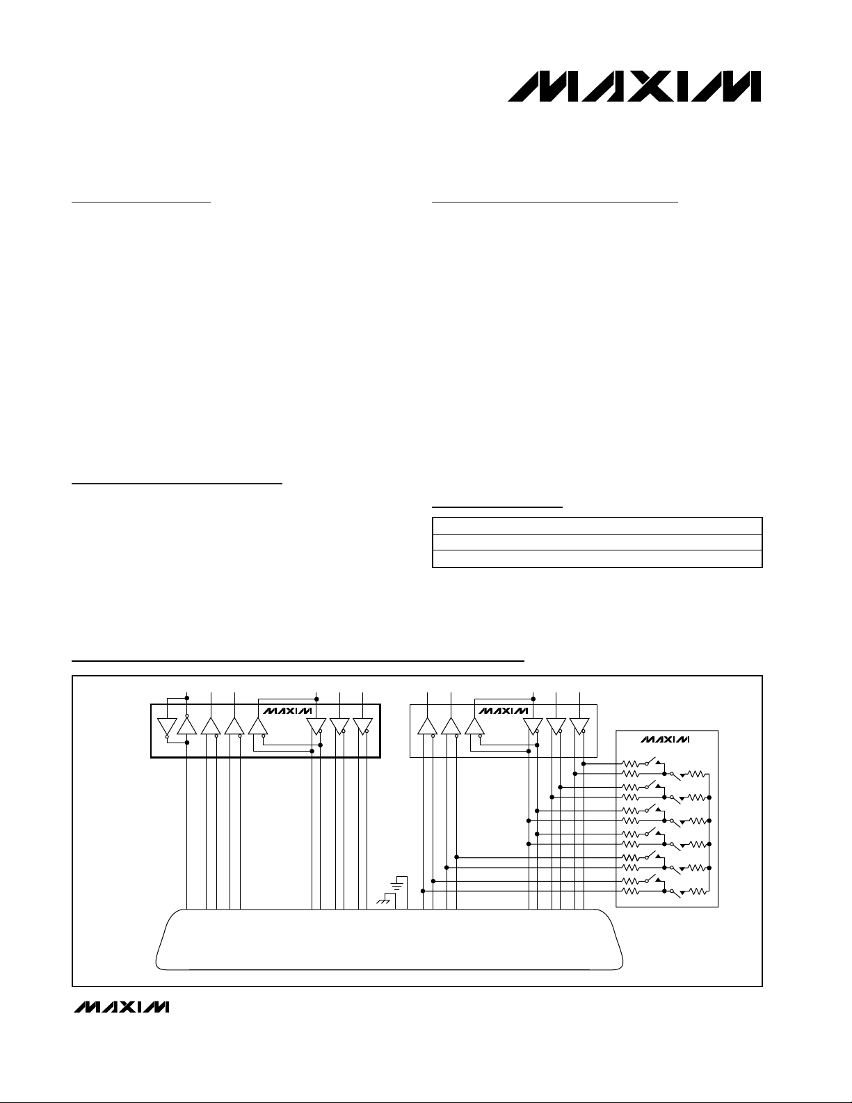
Typical Operating Circuit
Pin Configuration appears at end of data sheet.
For pricing, delivery, and ordering information, please contact Maxim/Dallas Direct! at
1-888-629-4642, or visit Maxim’s website at www.maxim-ic.com.
PART TEMP. RANGE PIN-PACKAGE
MXL1544CAI 0°C to +70°C 28 SSOP
MAX3175CAI 0°C to +70°C 28 SSOP
LL
CTS DSR RTSDTRDCD
MXL1544
MAX3175
D3
DCD B
R1
13
CTS A (106)
CTS B
R2R3
DSR A (109)
DSR B
R4
18 5 10 8 22 6 23 20 19 4 1 7 16 3 9 17 12 15 11 24 14 2
LL A (141)
DTR A (108)
DTR B
DCD A (107)
D1D2
RTS A (105)
RTS B
DB-25 CONNECTOR
RXD RXC TXDTXC SCTE
MXL1543
R1
R2R3
RXC B
RXD A (104)
RXD B
SG (102)
SHIELD (101)
RXC A (115)
D3D4
TXC A (114)
TXC B
SCTE A (113)
SCTE B
D1D2
TXD B
TXD A (103)
MXL1344A
Page 2
MXL1544/MAX3175
+5V Multiprotocol, Software-Selectable
Control Transceivers
2 _______________________________________________________________________________________
ABSOLUTE MAXIMUM RATINGS
ELECTRICAL CHARACTERISTICS
(VCC= +5V, VDD= +6.8V, VEE= -5.6V, TA= T
MIN
to T
MAX
, unless otherwise noted. Typical values are at TA= +25°C.) (Note 2)
Stresses beyond those listed under “Absolute Maximum Ratings” may cause permanent damage to the device. These are stress ratings only, and functional
operation of the device at these or any other conditions beyond those indicated in the operational sections of the specifications is not implied. Exposure to
absolute maximum rating conditions for extended periods may affect device reliability.
All Voltages to GND Unless Otherwise Noted
Supply Voltages
V
CC
.......................................................................-0.3V to +6V
V
DD
....................................................................-0.3V to +7.2V
V
EE
........................................................................+0.3V to -7V
V
DD
to VEE(Note 1)............................................................13V
Logic Input Voltage
M0, M1, M2, DCE/DTE, INVERT, T_IN..................-0.3V to +6V
Logic Output Voltage
R_OUT....................................................-0.3V to (V
CC
+ 0.3V)
Transmitter Outputs
T_OUT_, T_OUT_/R_IN........................................-15V to +15V
Short-Circuit Duration.............................................Continuous
Receiver Inputs
R_IN_, T_OUT_/R_IN_ .........................................-15V to +15V
Continuous Power Dissipation (T
A
= +70°C)
28-Pin SSOP (derate 11.1mW/°C above +70°C) .........889mW
Operating Temperature Range...............................0°C to +70°C
Junction Temperature......................................................+150°C
Storage Temperature Range .............................-65°C to +150°C
Lead Temperature (soldering, 10s) .................................+300°C
Note 1: VDDand VEE- can have maximum magnitude of 7.2V and 7V, respectively, but their difference cannot exceed 13V.
PARAMETER SYMBOL CONDITIONS MIN TYP MAX UNITS
POWER SUPPLIES
V
S up p l y C ur r ent ( D C E
C C
M od e) ( D i g i tal Inp uts = G N D or
V
) ( Tr ansm i tter s O utp uts
C C
S tati c)
VEE Supply Current (DCE
Mode) (Digital Inputs = GND
or V
) (Transmitters Outputs
CC
Static)
V
S up p l y C ur r ent ( D C E
D D
M od e) ( D i g i tal Inp uts = G N D or
V
) ( Tr ansm i tter s O utp uts
C C
S tati c)
Internal Power Dissipation
(DCE Mode)
LOGIC INPUTS (M0, M1, M2, DCE/DTE, INVERT, T1IN, T2IN, T3IN, T4IN)
Input High Voltage V
Input Low Voltage V
Logic Input Current I
I
CC
I
EE
I
DD
P
D
IH
IL
IN
RS-530, RS-530A, X.21, no load 2.7
RS-530, RS-530A, X.21, full load 95 120
V.28, no load 1 2
V.28, full load 1 2
No-cable mode, Invert = V
RS-530, RS-530A, X.21, no load 2.1
RS-530, X.21, full load 14
RS-530A, full load 25
V.28, no load 1
V.28, full load 12
No-cable mode 0.5 µA
RS-530, RS-530A, X.21, no load 0.6
RS-530, RS-530A, X.21, full load 1
V.28, no load 1
V.28, full load 12
No-cable mode 0.5 µA
RS-530, RS-530A, X.21, full load 300
V.28, full load 54
T1IN, T2IN, T3IN, T4IN ±10
M0, M1, M2, DCE/DTE, INVERT =
GND
M0, M1, M2, DCE/DTE, INVERT =
V
CC
C C
2.0 V
-100 -50 -30
0.5 10 µA
0.8 V
±10
mA
mA
mA
mW
µA
Page 3
MXL1544/MAX3175
+5V Multiprotocol, Software-Selectable
Control Transceivers
_______________________________________________________________________________________ 3
ELECTRICAL CHARACTERISTICS (continued)
(VCC= +5V, VDD= +6.8V, VEE= -5.6V, TA= T
MIN
to T
MAX
, unless otherwise noted. Typical values are at TA= +25°C.) (Note 2)
PARAMETER SYMBOL CONDITIONS MIN TYP MAX UNITS
LOGIC OUTPUTS (R1OUT, R2OUT, R3OUT, R4OUT)
Output High Voltage V
Output Low Voltage V
Output Short-Circuit Current I
Output Pullup Current I
OH
OL
SC
L
RECEIVER INPUTS
Receiver Glitch Rejection MAX3175 only 5 10 15 µs
V.11 TRANSMITTER
Open-Circuit Differential Output
Voltage
Loaded Differential Output
Voltage
Change in Magnitude of Output
Differential Voltage
Common-Mode Output Voltage V
Change in Magnitude of Output
Common-Mode Voltage
Short-Circuit Current I
Output Leakage Current I
V
V
∆V
∆V
ODO
ODL
OD
OC
OC
SC
Z
Rise or Fall Time tr, t
t
|t
PHL
t
PLH
PHL
t
PLH
Transmitter Input to Output
Data Skew
Output-to-Output Skew (Figures 2, 5) 3 ns
V.11 RECEIVER
Differential Input Voltage V
Input Hysteresis ∆V
Receiver Input Current I
Receiver Input Resistance R
TH
TH
IN
IN
Rise or Fall Time tr, t
t
|t
PHL
t
PLH
PHL
t
PLH
Receiver Input to Output
Data Skew
I
SOURCE
I
SINK
0 ≤ V
V
= 4mA 3 4.5 V
= 4mA 0.3 0.8 V
≤ V
OUT
CC
= 0, no-cable mode 70 µA
OUT
-50 50 mA
Op en ci r cui t, R = 1.95kΩ ( Fi g ur e 1) ±5V
R = 50Ω (Figure 1), TA = +25°C
0.5
V
✕
ODO
0.67
V
ODO
✕
R = 50Ω (Figure 1) ±2
R = 50Ω (Figure 1) 0.2 V
R = 50Ω (Figure 1) 3 V
R = 50Ω (Figure 1) 0.2 V
V
= GND 150 mA
OUT
-0.25V < V
cable mode
R = 50Ω (Figures 2, 5) 2 15 25 ns
f
,
R = 50Ω (Figures 2, 5) 50 75 ns
(Figures 2, 5) 3 12 ns
|
< +0.25V, power-off or no-
OUT
±1 ±100 µA
-7V ≤ VCM ≤ 7V -200 200 mV
-7V ≤ VCM ≤ 7V 15 40 mV
-10V ≤V
-10V ≤ V
(Figures 2, 6) 15 ns
f
,
(Figures 2, 6)
(Figures 2, 6)
|
≤ 10V ±0.66 mA
A,B
≤ 10V 15 30 kΩ
A,B
MXL1544 50 80 ns
MAX3175 10 µs
MXL1544 4 16 ns
MAX3175 1 µs
V
Page 4
MXL1544/MAX3175
+5V Multiprotocol, Software-Selectable
Control Transceivers
4 _______________________________________________________________________________________
ELECTRICAL CHARACTERISTICS (continued)
(VCC= +5V, VDD= +6.8V, VEE= -5.6V, TA= T
MIN
to T
MAX
, unless otherwise noted. Typical values are at TA= +25°C.) (Note 2)
PARAMETER SYMBOL CONDITIONS MIN TYP MAX UNITS
V.10 TRANSMITTER
Open-Circuit Output Voltage
Swing
Output Voltage Swing V
Short-Circuit Current I
Output Leakage Current I
Rise or Fall Time tr, t
Transmitter Input to Output
V.10 RECEIVER
Differential Threshold Voltage V
Input Hysteresis ∆V
Receiver Input Current I
Receiver Input Impedance R
Rise or Fall Time tr, t
V
t
PHL
t
PLH
t
PLH
O
T
SC
Z
f
TH
TH
IN
IN
f
Receiver Input to Output
t
PHL
|t
Data Skew
PHL
t
PLH
V.28 TRANSMITTER
Output Voltage Swing V
Short-Circuit Current I
Output Leakage Current I
O
SC
Z
Output Slew Rate SR RL = 3kΩ, CL = 2500pF (Figures 3, 7) 4 30 V/µs
t
Transmitter Input to Output
PHL
t
PLH
V.28 RECEIVER
Input Low Voltage V
Input High Voltage V
Input Hysteresis V
Input Resistance R
Rise or Fall Time tr, t
IL
IH
HYS
IN
f
RL = 3.9kΩ (Figure 3) ±4 ±6V
RL = 450Ω (Figure 3) ±3.6
RL = 450Ω (Figure 3), TA = +25°C
0.9 x
V
O
VO = GND, TA = +25°C ±150 mA
-0.25V < V
or no-cable mode
RL = 450Ω, C
,
RL = 450Ω, C
< +0.25V, power-off
OUT
= 100pF (Figures 3, 7) 2 µs
L
= 100pF (Figures 3, 7) 1 µs
L
±1 ±100 µA
-250 250 mV
25 50 mV
-10V ≤ VA ≤ 10V ±0.66 mA
-10V ≤ VA ≤ 10V 15 30 kΩ
(Figures 4, 8) 15 ns
MXL1544 55 ns
( Fi g ur es 4, 8)
MAX3175 10 µs
MXL1544 109 ns
MAX3175 10 µs
|
( Fi g ur es 4, 8)
MXL1544 60 ns
MAX3175 1 µs
Open circuit (Figure 3) ±7V
RL = 3kΩ (Figure 3) ±5 ±6V
VO = GND ±150 mA
-0.25V ≤ V
no-cable mode
RL = 3kΩ, C
≤ +0.25V, power-off or
OUT
= 2500pF (Figures 3, 7)
L
±1 ±100 µA
1.5 2.5
1.5 3
1.3 0.8 V
2.0 1.3 V
0.05 0.3 V
-15V < VIN < +15V 3 5 7 kΩ
(Figures 4, 8) 15 ns
V
µs
Page 5
MXL1544/MAX3175
+5V Multiprotocol, Software-Selectable
Control Transceivers
_______________________________________________________________________________________ 5
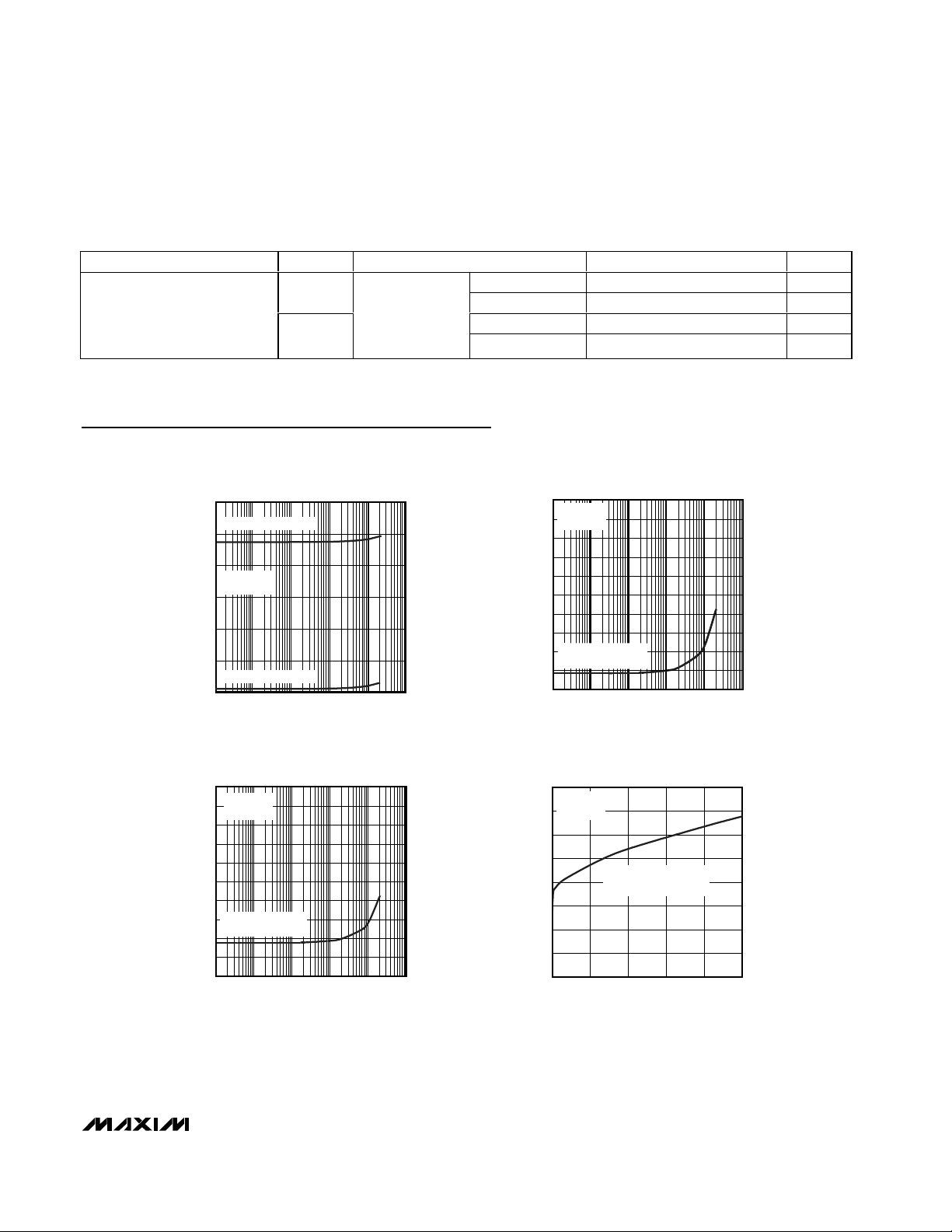
Typical Operating Characteristics
(TA = +25°C, unless otherwise noted.)
ELECTRICAL CHARACTERISTICS (continued)
(VCC= +5V, VDD= +6.8V, VEE= -5.6V, TA= T
MIN
to T
MAX
, unless otherwise noted. Typical values are at TA= +25°C.) (Note 2)
Note 2: MXL1544/MAX3175 are designed to operate with VDDand VEEsupplied by the MXL1543 charge pump.
0.65
0.66
0.67
0.68
0.69
0.70
0.71
0.72
0.73
0 50 100 150 200 250
V.28 MODE SUPPLY CURRENT (ICC)
vs. DATA RATE
MXL1544/MAX3175 toc04
DATA RATE (kbps)
I
CC
(mA)
DCE MODE
INVERT = 0
FULL LOAD (RL = 3kΩ,
C
L
= 2500) AND NO LOAD
PARAMETER SYMBOL CONDITIONS MIN TYP MAX UNITS
t
PLH
Receiver Input to Output
t
PHL
(Figures 4, 8)
MXL1544 60 100 ns
MAX3175 10 µs
MXL1544 70 450 ns
MAX3175 10 µs
V.11 MODE SUPPLY CURRENT (ICC)
vs. DATA RATE
120
FULL LOAD, R = 50Ω
100
80
DCE MODE
INVERT = 1
(mA)
60
CC
I
40
20
NO LOAD, R = 1.95kΩ
0
0.1 1 10 100 1000 10,000
DATA RATE (kbps)
MXL1544/MAX3175 toc01
(mA)
DD
I
V.11 MODE SUPPLY CURRENT (IDD)
vs. DATA RATE
10
DCE MODE
9
INVERT = 1
8
7
6
5
4
3
FULL, R = 50Ω
2
NO LOAD, R = 1.95kΩ
1
0
0.1 1 10 100 1000 10,000
DATA RATE (kbps)
MXL1544/MAX3175 toc02
(mA)
EE
I
V.11 MODE SUPPLY CURRENT (IEE)
vs. DATA RATE
10
DCE MODE
9
INVERT = 1
8
7
6
5
4
FULL, R = 50Ω
3
NO LOAD, R = 1.95kΩ
2
1
0
0.1 1 10 100 1000 10,000
DATA RATE (kbps)
MXL1544/MAX3175 toc03
Page 6
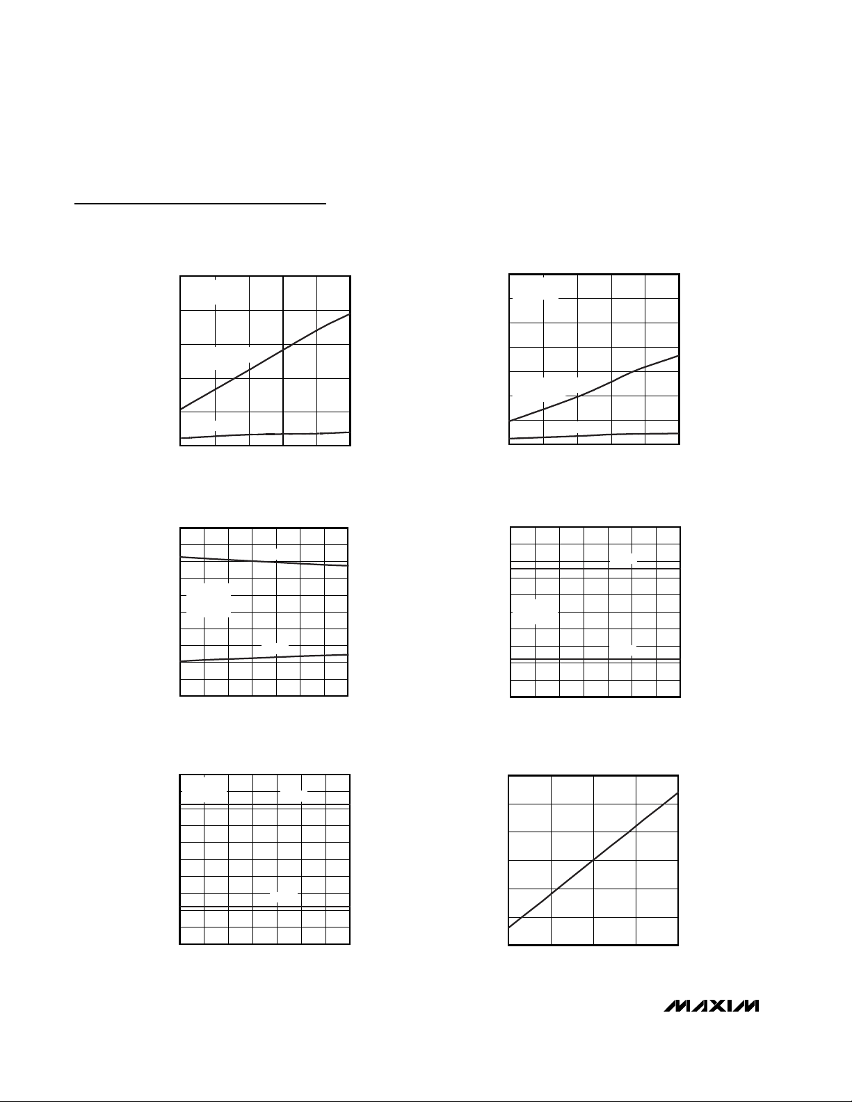
-300
-100
-200
100
0
200
300
-10 0-5 5 10
V.11 RECEIVER INPUT CURRENT
vs. INPUT VOLTAGE
MXL1544/MAX3175 toc10
INPUT VOLTAGE (V)
INPUT CURRENT (µA)
MXL1544/MAX3175
+5V Multiprotocol, Software-Selectable
Control Transceivers
6 _______________________________________________________________________________________
Typical Operating Characteristics (continued)
(TA = +25°C, unless otherwise noted.)
V.28 MODE SUPPLY CURRENT (IDD)
vs. DATA RATE
MXL1544/MAX3175 toc05
DATA RATE (kbps)
I
DD
(mA)
0
5
15
10
20
25
010050 150 200 250
DCE MODE
INVERT = 0
NO LOAD
FULL LOAD, RL = 3k
Ω,
CL = 2500pF
0
10
5
20
15
30
25
35
010050 150 200 250
V.28 MODE SUPPLY CURRENT (IEE)
vs. DATA RATE
MXL1544/MAX3175 toc06
DATA RATE (kbps)
I
EE
(mA)
DCE MODE
INVERT = 0
FULL LOAD, RL = 3kΩ,
C
L
= 2500pF
NO LOAD
-5
-2
-3
-4
0
-1
4
3
2
1
5
0 10203040506070
V.11 LOADED DIFFERENTIAL OUTPUT
VOLTAGE vs. TEMPERATURE
MXL1544/MAX3175 toc07
TEMPERATURE (°C)
DIFFERENTIAL OUTPUT VOLTAGE (V)
DCE MODE
INVERT = 1
R
L
= 50Ω
V
OUT+
V
OUT-
-10
-4
-6
-8
0
-2
8
6
4
2
10
0 10203040506070
V.28 LOADED OUTPUT VOLTAGE
vs. TEMPERATURE
MXL1544/MAX3175 toc09
TEMPERATURE (°C)
OUTPUT VOLTAGE (V)
DCE MODE
R
L
= 3kΩ
V
OUT-
V
OUT+
-10
-4
-6
-8
0
-2
8
6
4
2
10
0 10203040506070
V.10 LOADED OUTPUT VOLTAGE
vs. TEMPERATURE
MXL1544/MAX3175 toc08
TEMPERATURE (°C)
OUTPUT VOLTAGE (V)
V
OUT+
V
OUT-
DCE MODE
R
L
= 450Ω
Page 7

MXL1544/MAX3175
+5V Multiprotocol, Software-Selectable
Control Transceivers
_______________________________________________________________________________________ 7
Typical Operating Characteristics (continued)
(TA = +25°C, unless otherwise noted.)
V.28 RECEIVER INPUT CURRENT
vs. INPUT VOLTAGE
5
4
3
2
1
0
-1
INPUT CURRENT (mA)
-2
-3
-4
-5
-15 -5-10 0 5 10 15
INPUT VOLTAGE (V)
V.10 TRANSMITTER RISE AND FALL TIME
vs. LOAD CAPACITANCE
3.5
3.0
2.5
2.0
1.5
RISE/FALL TIME (µs)
1.0
0.5
RISE
FALL
V.28 SLEW RATE vs. LOAD CAPACITANCE
18
16
14
MXL1544/MAX3175 toc11
MXL1544/MAX3175 toc13
12
10
8
SLEW RATE (V/µs)
6
4
2
0
020001000 3000 4000 5000
SLEW+
SLEW-
CAPACITANCE (pF)
MXL1544 LOOPBACK SCOPE PHOTO
V.11 MODE (UNLOADED)
T
IN
T
/
OUT
R
IN
R
OUT
MXL1544/MAX3175 toc14
MXL1544/MAX3175 toc12
5V/div
5V/div
5V/div
0
0 1000 1500500 2000 2500 3000
CAPACITANCE (pF)
MXL1544 LOOPBACK SCOPE PHOTO
V.28 MODE (LOADED)
T
IN
T
/
OUT
R
IN
R
OUT
MXL1544/MAX3175 toc15
4µs/div
5V/div
5V/div
5V/div
MXL1544 LOOPBACK SCOPE PHOTO
T
IN
T
/
OUT
R
IN
R
OUT
4µs/div
V.10 MODE (LOADED)
MXL1544/MAX3175 toc16
4µs/div
5V/div
5V/div
5V/div
Page 8

MXL1544/MAX3175
+5V Multiprotocol, Software-Selectable
Control Transceivers
8 _______________________________________________________________________________________
Pin Description
PIN NAME FUNCTION
1VCC+5V Supply Voltage (±5%). Bypass with a 1µF capacitor to ground.
2VDDPositive Supply Generated by MXL1543. Bypass with a 1µF capacitor to ground.
3 T1IN Transmitter 1 TTL-Compatible Input
4 T2IN Transmitter 2 TTL-Compatible Input
5 T3IN Transmitter 3 TTL-Compatible Input
6 R1OUT Receiver 1 CMOS Output
7 R2OUT Receiver 2 CMOS Output
8 R3OUT Receiver 3 CMOS Output
9 T4IN Transmitter 4 TTL-Compatible Input
10 R4OUT Receiver 4 CMOS Output
11 M0 TTL-Compatible Mode Select Pin with Internal Pullup to V
12 M1 TTL-Compatible Mode Select Pin with Internal Pullup to V
13 M2 TTL-Compatible Mode Select Pin with Internal Pullup to V
14 DCE/DTE TTL-Compatible Input with Internal Pullup to VCC. Logic level high selects DCE interface.
15 INVERT TTL Inp ut w i th Inter nal P ul l up to V
16 T4OUTA/R4INA Transmitter Output/Inverting Receiver Input
17 R3INB Noninverting Receiver Input
18 R3INA Inverting Receiver Input
19 R2INB Noninverting Receiver Input
20 R2INA Inverting Receiver Input
21 T3OUTB/R1INB Noninverting Transmitter Output/Noninverting Receiver Input
22 T3OUTA/R1INA Inverting Transmitter Output/Inverting Receiver Input
23 T2OUTB Noninverting Transmitter Output
24 T2OUTA Inverting Transmitter Output
25 T1OUTB Noninverting Transmitter Output
26 T1OUTA Inverting Transmitter Output
27 GND Ground
28 V
EE
Negative Supply Generated by MXL1543. Bypass with a 1µF capacitor to ground.
CC
CC
CC
. IN V E RT = H IGH r ever ses acti on of D C E /DTE for C hannel 4.
C C
Page 9

MXL1544/MAX3175
+5V Multiprotocol, Software-Selectable
Control Transceivers
_______________________________________________________________________________________ 9
Detailed Description
The MXL1544/MAX3175 are four-driver/four-receiver
multiprotocol transceivers that operate from a single
+5V supply and the charge pump from the MXL1543.
The MXL1544/MAX3175, along with the MXL1543 and
MXL1344A, form a complete software-selectable DTE
or DCE interface port that supports the V.28 (RS-232),
V.10/V.11 (RS-449, V.36, EIA-530, EIA-530A, X.21, RS-
423), and V.35 protocols. The MXL1544 or MAX3175
usually carries the control signals. The MXL1543 carries the high-speed clock and data signals, and the
MXL1344A provides termination for the clock and data
signals.
The MXL1544/MAX3175 feature a 0.5µA no-cable
mode, true fail-safe operation, and thermal shutdown
circuitry. Thermal shutdown protects the drivers against
excessive power dissipation. When activated, the thermal shutdown circuitry places the driver outputs into a
high-impedance state. The MAX3175 deglitching feature reduces errors in unterminated equipment.
The state of the mode-select pins M0, M1, and M2
determines which serial-interface protocol is selected
(Table 1). The state of the DCE/DTE input determines
whether the transceivers will be configured as a DTE
serial port or a DCE serial port. When the DCE/DTE
input is logic HIGH, driver T3 is activated and receiver
R1 is disabled. When the DCE/DTE input is logic LOW,
driver T3 is disabled and receiver R1 is activated. The
INVERT pin state changes the DCE/DTE functionality
regarding T4 and R4 only. M0, M1, M2, INVERT, and
DCE/DTE are internally pulled up to V
CC
to ensure logic
HIGH if left unconnected.
Figure 1. V.11 DC Test Circuit
Figure 3. V.10/V.28 Driver Test Circuit
Figure 2. V.11 AC Test Circuit
Figure 4. V.10/V.28 Receiver Test Circuit
Test Circuits
V
OD
B
D
A
100Ω
100pF
R
V
R
B
A
OC
R
15pF
DA
V
C
O
L
DAR
R
L
15pF
100pF
Page 10

MXL1544/MAX3175
+5V Multiprotocol, Software-Selectable
Control Transceivers
10 ______________________________________________________________________________________
Figure 5. V.11, V.35 Driver Propagation Delays
Figure 6. V.11, V.35 Receiver Propagation Delays
Figure 7. V.10, V.28 Driver Propagation Delays
Figure 8. V.10, V.28 Receiver Propagation Delays
Switching Time Waveforms
5V
B-A
D
0
V
0
-V
0
A
B
V
1.5V
t
PLH
50%
0
90%
10%
t
r
t
SKEW
V
0D2
-V
0D2
V
0H
R
V
0L
B-A
0
t
PLH
1.5V
3V
D
0
V
0
A
-V
0
1.5V
t
PHL
3V
0
t
f
f = 1MHz: tr ≤ 10ns: tf ≤ 10ns
V
DIFF
1/2 V
0
f = 1MHz: tr ≤ 10ns: tf ≤ 10ns
-3V
= V(B) - V(A)
INPUT
OUTPUT
1.5V
0
t
PHL
90%
t
PLH
-3V
50%
10%
t
f
t
SKEW
0
t
PHL
1.5V
3V
0
t
r
V
IH
A
V
IL
V
0H
R
V
0L
1.3V
t
PHL
0.8V
1.7V
t
PLH
2.4V
Page 11

MXL1544/MAX3175
+5V Multiprotocol, Software-Selectable
Control Transceivers
______________________________________________________________________________________ 11
The MXL1544/MAX3175s’ mode can be selected
through software control of the M0, M1, M2, INVERT,
and DCE/DTE inputs. Alternatively, the mode can be
selected by shorting the appropriate combination of
mode control inputs to GND (the inputs left floating will
be internally pulled up to VCC- logic HIGH). If the M0,
M1, and M2 mode inputs are all unconnected, the
MXL1544/MAX3175 will enter no-cable mode.
Fail-Safe
The MXL1544/MAX3175 guarantee a logic HIGH
receiver output when the receiver inputs are shorted or
open, or when they are connected to a terminated
transmission line with all drivers disabled. The V.11
receiver threshold is set between -200mV and 0mV to
guarantee fail-safe operation. If the differential receiver
input voltage (B - A) is ≥ 0mV, ROUT is logic HIGH. In
the case of a terminated bus with all transmitters disabled, the receiver’s differential input voltage is pulled
to 0 by the termination. With the receiver thresholds of
the MXL1544/MAX3175, this results in ROUT logic
HIGH.
The V.10 receiver threshold is set between -250mV and
0mV. If the V.10 receiver input voltage is less than or
equal to -250mV, ROUT is logic HIGH. The V.28 receiver threshold is set between 0.8V and 2.0V. If the receiver input voltage is less than or equal to 0.8V, ROUT is
logic HIGH. In the case of a terminated bus with transmitters disabled, the receiver’s input voltage is pulled
to 0 by the termination.
Applications Information
Cable-Selectable Mode
A cable-selectable, multiprotocol DTE/DCE interface is
shown in Figure 9. The mode control lines M0, M1, and
DCE/DTE are wired to the DB-25 connector. To select
the serial interface mode, the appropriate combination
of M0, M1, M2, and DCE/DTE are grounded within the
cable wiring. The control lines that are not grounded
are pulled high by the internal pullups on the MXL1543.
The serial interface protocol of the MXL1544/MAX3175
is now selected based on the cable that is connected
to the DB-25 interface.
V.10 (RS-423) Interface
The V.10 interface (Figure 10) is an unbalanced singleended interface capable of driving a 450Ω load. The
V.10 driver generates a minimum VOvoltage of ±4V
across A’ and C’ when unloaded and a minimum voltage of 0.9 ✕VOwhen loaded with 450Ω. The V.10
receiver has a single-ended input and does not reject
common-mode differences between C and C’. The V.10
receiver input trip threshold is defined between
+250mV and -250mV with input impedance characteristic shown in Figure 11.
The MXL1544/MAX3175 V.10 mode receiver has a differential threshold between -250mV and +250mV. To
ensure that the receiver has proper fail-safe operation
see the Fail-Safe section. To aid in rejecting system
noise, the MXL1544/MAX3175 V.10 receiver has a typical hysteresis of 25mV. Switch S3 in Figure 12 is open
in V.10 mode to disable the V.28 5kΩ termination at the
receiver input. Switch S4 is closed and switch S5 is
open to internally ground the receiver B input.
V.11 (RS-422) Interface
As shown in Figure 13, the V.11 protocol is a fully balanced differential interface. The V.11 driver generates a
minimum of ±2V between nodes A and B when 100Ω
minimum resistance is presented at the load. The V.11
receiver is sensitive to differential signals of ±200mV at
receiver inputs A’ and B’. The V.11 receiver input must
comply with the impedance curve of Figure 11 and
reject common-mode signals developed across the
cable (referenced from C to C’ in Figure 13) of up to
±7V.
The MXL1544/MAX3175 V.11 mode receiver has a differential threshold between -200mV and +200mV. To
ensure that the receiver has proper fail-safe operation;
see the Fail-Safe section. To aid in rejecting system
noise, the MXL1544/MAX3175 V.11 receiver has a typical hysteresis of 15mV. Switch S3 in Figure 14 is open
in V.11 mode to disable the V.28 5kΩ termination at the
inverting receiver input. Because the control signals are
slow (60kbps), 100Ω termination resistance is generally
not required for the MXL1544/MAX3175. The receiver
inputs must also be compliant with the impedance
curve shown in Figure 11.
V.28 (RS-232) Interface
The V.28 interface is an unbalanced single-ended interface (Figure 10). The V.28 generator provides a minimum of ±5V across the 3kΩ load impedance between
A’ and C’. The V.28 receiver has single-ended input.
The MXL1544/MAX3175 V.28 mode receiver has a
threshold between +0.8V and +2.0V. To aid in rejecting
system noise, the MXL1544/MAX3175 V.28 receiver
has a typical hysteresis of 50mV. Switch S3 in Figure 15
is closed in V.28 mode to enable the 5kΩ V.28 termination at the receiver inputs.
No-Cable Mode
The MXL1544/MAX3175 will enter no-cable mode when
the mode-select pins are left unconnected or connected HIGH (M0 = M1 = M2 = 1). In this mode, the multiprotocol drivers and receivers are disabled and the
Page 12

MXL1544/MAX3175
+5V Multiprotocol, Software-Selectable
Control Transceivers
12 ______________________________________________________________________________________
Figure 9. Cable-Selectable Multiprotocol DCE/DTE Port with DB-25 Connector
C6
100pFC7100pFC8100pF
3
8111213
V
CC
5V
1µF
C1
C4
1µF
NC
V
NC
10
11
12
13
14
CC
10
11
12
13
14
3
1
CHARGE
2
PUMP
4
5
D1
6
D2
7
D3
8
R1
9
R2
R3
MXL1543
M0
M1
M2
DCE/DTE
1
V
CC
2
V
DD
3
D1
4
D2
5
D3
6
R1
7
R2
8
R3
R4
9
D4
MXL1544
M0
MAX3175
M1
M2
DCE/DTE INVERT
C3
4.7µF
DTE_TXD/DCE_RXD
DTE_SCTE/DCE_RXC
DTE_TXC/DCE_TXC
DTE_RXC/DCE_SCTE
DTE_RXD/DCE_TXD
C10
1µF
DTE_RTS/DCE_CTS
DTE_DTR/DCE_DSR
DTE_DCD/DCE_DCD
DTE_DSR/DCE_DTR
DTE_CTS/DCE_RTS
1µF
C9
GND
14
V
C13
C2
1µF
C5
4.7µF
1µF
MODE
V.35
RS-449. V.36
RS-232
28
27
26
25
24
23
22
21
20
19
18
17
16
15
28
V
EE
27
26
25
24
23
22
21
20
19
18
17
16
15
CC
2
V
EE
C12
1µF
C11
1µF
CABLE WIRING FOR
MODE SELECTION
PIN 18
PIN 7
N.C.
PIN 7
4 6 7 9 10 16 15 18 17 19 20 22 23 24 15
PIN 21
PIN 7
PIN 7
N.C.
CABLE WIRING FOR
DTE/DCE SELECTION
PIN 25
MODE
PIN 7
DTE
N.C.
DCE
MXL1344A
DCE/DTE
M2
V
CC
LATCH
M1
21
M0
DCE
DTE
2
RXD A
TXD A
14
RXD B
TXD B
24
RXC A
SCTE A
11
RXC B
SCTE B
15
TXC A
TXC A
12
TXC B
TXC B
17
SCTE A
RXC A
9
SCTE B
RXC B
3
TXD A
RXD A
16
TXD B
RXD B
7
SG
1
SHIELD
DB-25
CONNECTOR
25
DCE/DTE
21
M1
18
M0
4
CTS A
RTS A
19
RTS B
20
23
10
22
13
CTS B
DSR A
DTR A
DTR B
DSR B
8
DCD A
DCD A
DCD B
DCD B
6
DTR A
DSR A
DTR B
DSR B
5
RTS A
CTS A
RTS B
CTS B
Page 13

MXL1544/MAX3175
+5V Multiprotocol, Software-Selectable
Control Transceivers
______________________________________________________________________________________ 13
supply current is less than 10µA. The receiver outputs
enter a high-impedance state in no-cable mode, which
allows these output lines to be shared with other receiver outputs (the receiver outputs have an internal pullup
resistor to pull the outputs HIGH if not driven). Also, in
no-cable mode, the transmitter outputs enter a highimpedance state, so these output lines can be shared
with other devices.
Receiver Glitch Rejection
To improve operation in an unterminated or otherwise
noisy system, the MAX3175 features 10µs of receiver
input glitch rejection. The glitch-rejection circuitry
blocks the reception of high-frequency noise (tB< 5µs)
while receiving a low-frequency signal (t
B
>15µs) allowing glitch-free operation in unterminated systems at up
to 60kbps. The MXL1544 does not have this feature
and can be operated at frequencies greater than
60kbps if properly terminated.
Figure 10. Typical V.10/V.28 Interface
Figure 11. Receiver Input Impedance Curve
Figure 12. V.10 Internal Resistance Network
Figure 13. Typical V.11 Interface
GENERATOR
I
Z
-10V
-3.25mA
-3V
+3V
A
C
UNBALANCED
INTERCONNECTING
CABLE
3.25mA
V
Z
+10V
LOAD
CABLE
TERMINATION
A′
C′
BALANCED
GENERATOR
INTERCONNECTING
A
B
C
CABLE
RECEIVER
TERMINATION
A′
B′
C′
CABLE
100Ω
MIN
LOAD
RECEIVER
A′
A
R5
30kΩ
R8
5kΩ
S3
R4
GND
30kΩ
S4
B′
B
C′
10kΩ
10kΩ
S5
R6
R7
MXL1544
MAX3175
RECEIVER
Page 14

MXL1544/MAX3175
+5V Multiprotocol, Software-Selectable
Control Transceivers
14 ______________________________________________________________________________________
DTE vs. DCE Operation
Figure 16 shows a port with one DB-25 connector that
can be configured for either DTE or DCE operation. The
configuration requires separate cables for proper signal routing in DTE or DCE operation. Figure 16 illustrates a DCE or DTE controller-selectable interface. The
DCE/DTE and INVERT inputs switch the port’s mode of
operation (Table 1).
The MXL1543 and MXL1544/MAX3175 can be connected for either DTE or DCE operation in one of two ways:
a dedicated DTE or DCE port with an appropriate gender connector or a port with a connector that can be
configured for DTE or DCE operation by rerouting the
signals to the MXL1543 and MXL1544/MAX3175 using
a dedicated DTE cable or dedicated DCE cable. The
interface mode is selected by logic outputs from the
controller or from jumpers to either VCCor GND on the
mode select pins. A dedicated DCE port using a DB-25
female connector is shown in Figure 17. Figure 18 illustrates a dedicated DTE port using a DB-25 male connector.
Figure 15. V.28 Termination and Internal Resistance NetworkFigure 14. V.11 Internal Resistance Networks
A′
A
R5
30kΩ
R8
5kΩ
10kΩ
R6
MXL1544
MAX3175
RECEIVER
A′
A
R5
30kΩ
R8
5kΩ
10kΩ
R6
MXL1544
MAX3175
RECEIVER
S3
R7
R4
B
B′
C′
30kΩ
GND
10kΩ
S3
R7
10kΩ
R4
B′
B
C′
GND
30kΩ
Page 15

MXL1544/MAX3175
+5V Multiprotocol, Software-Selectable
Control Transceivers
______________________________________________________________________________________ 15
Table 1. Mode Select Table
PROTOCOL M2 M1 M0
Not Used
(Default V.11)
RS-530A 0 0 1 0 0 V.11 V.10 Z V.11 V.10 V.11 Z V.10
RS-530 0 1 0 0 0 V.11 V.11 Z V.11 V.11 V.11 Z V.10
X.21 0 1 1 0 0 V.11 V.11 Z V.11 V.11 V.11 Z V.10
V.35 1 0 0 0 0 V.28 V.28 Z V.28 V.28 V.28 Z V.28
RS-449/V.36 1 0 1 0 0 V.11 V.11 Z V.11 V.11 V.11 Z V.10
V.28/RS-232 1 1 0 0 0 V.28 V.28 Z V.28 V.28 V.28 Z V.28
No Cable 1 1 1 0 0 Z Z Z Z Z Z Z Z
Not Used
(Default V.11)
RS-530A 0 0 1 0 1 V.11 V.10 Z V.11 V.10 V.11 V.10 Z
RS-530 0 1 0 0 1 V.11 V.11 Z V.11 V.11 V.11 V.10 Z
X.21 0 1 1 0 1 V.11 V.11 Z V.11 V.11 V.11 V.10 Z
V.35 1 0 0 0 1 V.28 V.28 Z V.28 V.28 V.28 V.28 Z
RS-449/V.36 1 0 1 0 1 V.11 V.11 Z V.11 V.11 V.11 V.10 Z
V.28/RS-232 1 1 0 0 1 V.28 V.28 Z V.28 V.28 V.28 V.28 Z
No Cable 1 1 1 0 1 Z Z Z Z Z Z Z Z
Not Used
(Default V.11)
RS-530A 0 0 1 1 0 V.11 V.10 V.11 Z V.10 V.11 V.10 Z
RS-530 0 1 0 1 0 V.11 V.11 V.11 Z V.11 V.11 V.10 Z
X.21 0 1 1 1 0 V.11 V.11 V.11 Z V.11 V.11 V.10 Z
V.35 1 0 0 1 0 V.28 V.28 V.28 Z V.28 V.28 V.28 Z
RS-449/V.36 1 0 1 1 0 V.11 V.11 V.11 Z V.11 V.11 V.10 Z
V.28/RS-232 1 1 0 1 0 V.28 V.28 V.28 Z V.28 V.28 V.28 Z
No Cable 1 1 1 1 0 Z Z Z Z Z Z Z Z
Not Used
(Default V.11)
RS-530A 0 0 1 1 1 V.11 V.10 V.11 Z V.10 V.11 Z V.10
RS-530 0 1 0 1 1 V.11 V.11 V.11 Z V.11 V.11 Z V.10
X.21 0 1 1 1 1 V.11 V.11 V.11 Z V.11 V.11 Z V.10
V.35 1 0 0 1 1 V.28 V.28 V.28 Z V.28 V.28 Z V.28
RS-449/V.36 1 0 1 1 1 V.11 V.11 V.11 Z V.11 V.11 Z V.10
V.28/RS-232 1 1 0 1 1 V.28 V.28 V.28 Z V.28 V.28 Z V.28
No Cable 1 1 1 1 1 Z Z Z Z Z Z Z Z
0 0 0 0 0 V.11 V.11 Z V.11 V.11 V.11 Z V.10
0 0 0 0 1 V.11 V.11 Z V.11 V.11 V.11 V.10 Z
0 0 0 1 0 V.11 V.11 V.11 Z V.11 V.11 V.10 Z
0 0 0 1 1 V.11 V.11 V.11 Z V.11 V.11 Z V.10
DCE/
DTE
INVERT T1 T2 T3 R1 R2 R3 T4 R4
Page 16

MXL1544/MAX3175
+5V Multiprotocol, Software-Selectable
Control Transceivers
16 ______________________________________________________________________________________
Figure 16. Controller-Selectable Multiprotocol DCE/DTE Port with DB-25 Connector
C6
100pFC7100pFC8100pF
3
8111213
V
CC
5V
1µF
3
1
C1
C4
1µF
10
11
12
13
14
2
4
5
6
7
8
9
CHARGE
D1
D2
D3
MXL1543
M0
M1
M2
DCE/DTE
PUMP
R1
R2
R3
C3
4.7µF
DTE_TXD/DCE_RXD
DTE_SCTE/DCE_RXC
DTE_TXC/DCE_TXC
DTE_RXC/DCE_SCTE
DTE_RXD/DCE_TXD
14
V
C12
1µF
CC
2
V
EE
4 6 7 9 10 16 15 18 17 19 20 22 23 24 15
C13
C2
1µF
C5
4.7µF
1µF
28
27
26
25
24
23
22
21
20
19
18
17
16
15
MXL1344A
DCE/DTE
21
LATCH
M2
M1
M0
DCE
DTE
2
RXD A
TXD A
14
RXD B
TXD B
24
RXC A
SCTE A
11
RXC B
SCTE B
15
TXC A
TXC A
12
TXC B
TXC B
17
SCTE A
RXC A
9
SCTE B
RXC B
3
TXD A
RXD A
16
TXD B
RXD B
7
SG
1
SHIELD
C10
1µF
DTE_RTS/DCE_CTS
DTE_DTR/DCE_DSR
DTE_DCD/DCE_DCD
DTE_DSR/DCE_DTR
DTE_CTS/DCE_RTS
DTE_LL/DCE_LL
INVERT
DCE/DTE
DB-25
4
19
20
23
8
10
6
22
5
13
18
CONNECTOR
RTS A
RTS B
DTR A
DTR B
DCD A
DCD B
DSR A
DSR B
CTS A
CTS B
LL A
CTS A
CTS B
DSR A
DSR B
DCD A
DCD B
DTR A
DTR B
RTS A
RTS B
LL A
C9
V
CC
1µF
M2
M1
M0
10
11
12
13
14
1
2
3
4
5
6
7
8
9
V
CC
V
DD
MXL1544
M0
MAX3175
M1
M2
DCE/DTE
28
V
EE
27
GND
26
D1
25
24
D2
23
D3
22
21
R1
20
R2
19
18
R3
17
16
R4
D4
15
INVERT
C11
1µF
Page 17

MXL1544/MAX3175
+5V Multiprotocol, Software-Selectable
Control Transceivers
______________________________________________________________________________________ 17
Figure 17. Controller-Selectable DCE Port with DB-25 Connector
C10
1µF
RXD
RXC
TXC
SCTE
TXD
CTS
DSR
DCD
DTR
RTS
INVERT
C6
100pFC7100pFC8100pF
3
8111213
V
CC
5V
1µF
3
1
C1
2
4
C4
1µF
5
6
7
8
9
10
11
MXL1543
M0
12
M1
13
M2
14
NC
DCE/DTE
V
CC
1
V
CC
2
V
DD
3
4
5
6
7
8
10
9
MXL1544
11
M0
MAX3175
12
M1
13
M2
14
NC
DCE/DTE
C3
4.7µF
C9
1µF
LL
M2
M1
M0
CHARGE
PUMP
D1
D2
D3
R1
R2
R3
D1
D2
D3
R1
R2
R3
R4
D4
GND
INVERT
28
C2
1µF
27
26
C5
4.7µF
25
24
23
22
21
20
19
18
17
16
15
28
V
EE
27
26
25
24
23
22
21
20
19
18
17
16
15
1µF
C13
C11
1µF
14
C12
1µF
V
CC
2
V
EE
4 6 7 9 10 16 15 18 17 19 20 22 23 24 15
V
CC
DCE/DTE
MXL1344A
M2
LATCH
M1
21
M0
3
RXD A (104)
16
RXD B
17
RXC A (115)
9
RXC B
15
TXC A (114)
12
TXC B
24
SCTE A (113)
11
SCTE B
2
TXD A (103)
14
TXD B
7
SGND (102)
1
SHIELD (101)
DB-25
FEMALE
CONNECTOR
5
CTS A (106)
13
CTS B
6
DSR A (107)
22
DSR B
8
DCD A (109)
10
DCD B
20
DTR A (108)
23
DTR B
4
RTS A (105)
19
RTS B
18
LL A (141)
Page 18

MXL1544/MAX3175
+5V Multiprotocol, Software-Selectable
Control Transceivers
18 ______________________________________________________________________________________
Figure 18. Controller-Selectable Multiprotocol DTE Port with DB-25 Connector
C6
100pFC7100pFC8100pF
3
8111213
V
CC
5V
1µF
3
1
C1
C4
1µF
10
11
12
13
14
2
4
5
6
7
8
9
CHARGE
D1
D2
D3
MXL1543
M0
M1
M2
DCE/DTE
PUMP
R1
R2
R3
C3
4.7µF
TXD
SCTE
TXC
RXC
RXD
14
V
C12
1µF
CC
2
V
EE
4 6 7 9 10 16 15 18 17 19 20 22 23 24 15
C13
C2
1µF
C5
4.7µF
1µF
28
27
26
25
24
23
22
21
20
19
18
17
16
15
MXL1344A
DCE/DTE
M2
LATCH
M1
21
M0
2
TXD A (103)
14
TXD B
24
SCTE A (113)
11
SCTE B
15
TXC A (114)
12
TXC B
17
RXC A (115)
9
RXC B
3
RXD A (104)
16
RXD B
7
SG
1
SHIELD
C9
V
CC
C10
1µF
RTS
DTR
DCD
DSR
CTS
INVERT
1µF
LL
M2
M1
M0
10
11
12
13
14
1
2
3
4
5
6
7
8
9
V
CC
V
DD
MXL1544
M0
MAX3175
M1
M2
DCE/DTE
28
V
EE
27
GND
26
D1
25
24
D2
23
D3
22
21
R1
20
R2
19
18
R3
17
16
R4
D4
15
INVERT
C11
1µF
4
19
20
23
8
10
6
22
5
13
18
DB-25 MALE
CONNECTOR
RTS A (105)
RTS B
DTR A (108)
DTR B
DCD A (109)
DCD B
DSR A (107)
DSR B
CTS A (106)
CTS B
LL A (141)
Page 19

MXL1544/MAX3175
+5V Multiprotocol, Software-Selectable
Control Transceivers
______________________________________________________________________________________ 19
Pin Configuration
Chip Information
TRANSISTOR COUNT: 2348
PROCESS: BiCMOS
TOP VIEW
V
V
T1IN
T2IN
T3IN
R1OUT
R2OUT
R3OUT
T4IN
R4OUT
DCE/DTE
M0
M1
M2
1
CC
2
DD
3
4
5
MXL1544
6
MAX3175
7
8
9
10
11
12
13
14
28
V
EE
27
GND
26
T1OUTA
25
T1OUTB
24
T2OUTA
23
T2OUTB
22
T3OUTA/R1INA
21
T3OUTB/R1INB
20
R2INA
19
R2INB
18
R3INA
17
R3INB
16
T4OUTA/R4INA
15
INVERT
SSOP
Page 20

MXL1544/MAX3175
+5V Multiprotocol, Software-Selectable
Control Transceivers
Maxim cannot assume responsibility for use of any circuitry other than circuitry entirely embodied in a Maxim product. No circuit patent licenses are
implied. Maxim reserves the right to change the circuitry and specifications without notice at any time.
20 ____________________Maxim Integrated Products, 120 San Gabriel Drive, Sunnyvale, CA 94086 408-737-7600
© 2001 Maxim Integrated Products Printed USA is a registered trademark of Maxim Integrated Products.
Package Information
SSOP.EPS
 Loading...