

Page 1
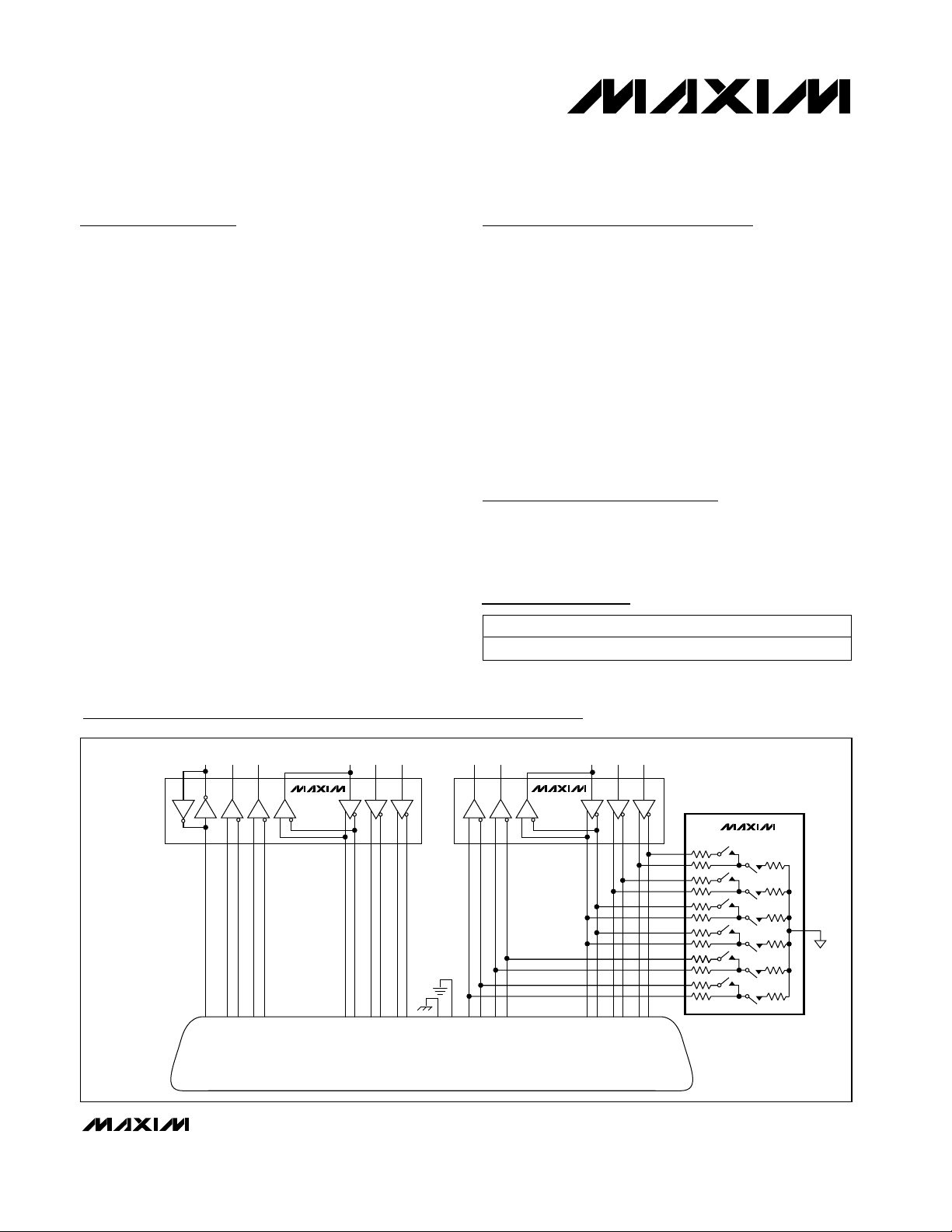
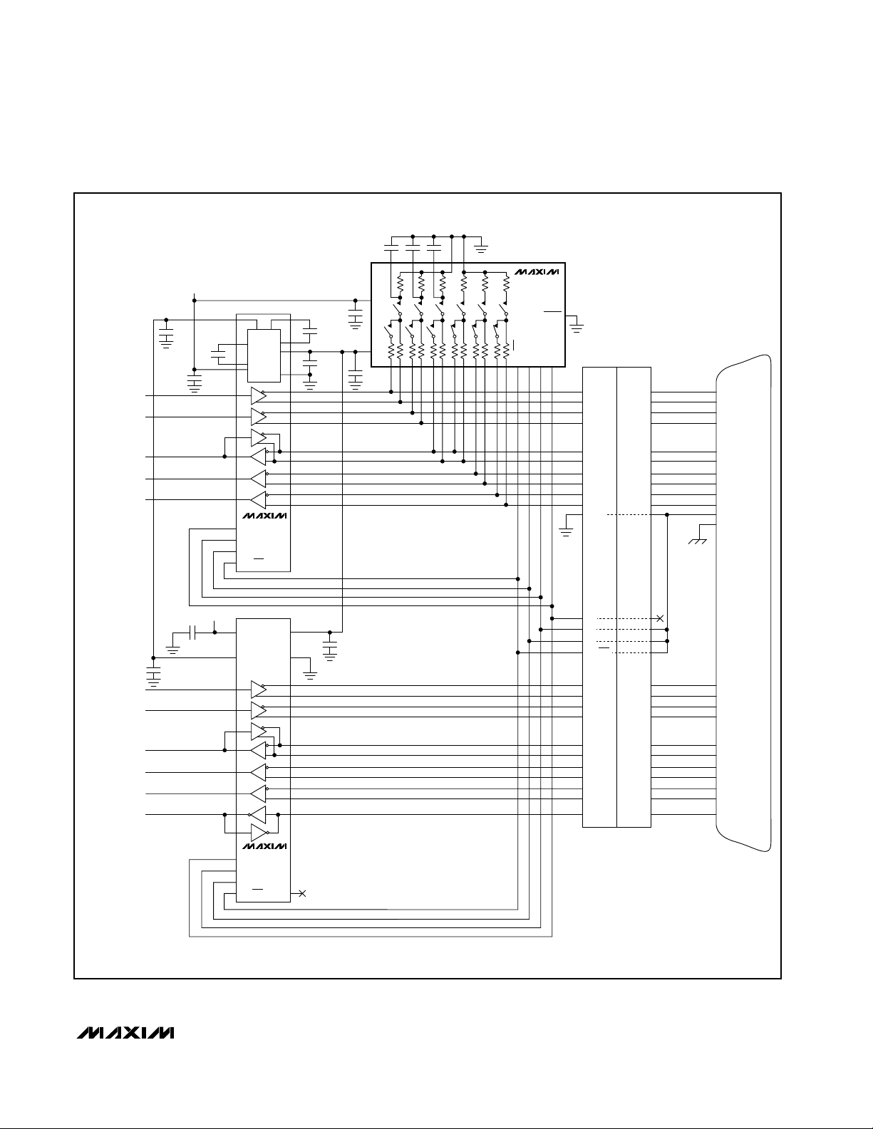
Typical Operating Circuit
For price, delivery, and to place orders, please contact Maxim Distribution at 1-888-629-4642,
or visit Maxim’s website at www.maxim-ic.com.
General Description
The MXL1344A contains six software-selectable, multiprotocol cable termination networks. Each network is
capable of terminating V.11 (RS-422, RS-530, RS-530A,
RS-449, V.36 and X.21) with a 100Ω differential load,
V.35 with a T-network load, or V.28 (RS-232) and V.10
(RS-423) with an open-circuit load for use with transceivers having on-chip termination. The termination protocol can be selected by the serial interface cable
wiring or by software control. The MXL1344A replaces
discrete resistor termination networks and expensive
relays required for multiprotocol termination, saving
space and cost.
The MXL1344A terminator is designed to form a complete +5V cable- or software-selectable multiprotocol
DCE/DTE interface port when used with the MXL1543
and MXL1544/MAX3175 transceiver ICs. The MXL1344A
terminator can use the VEEpower generated by the
MXL1543 charge pump, simplifying system design. The
MXL1344A, MXL1543, and MXL1544/MAX3175 are pinfor-pin compatible with the LTC1344A, LTC1543, and
LTC1544, but for proper operation the entire Maxim
chipset must be used without substituting other manufacturer's parts on a chip-by-chip basis.
The MXL1344A is available in a 24-pin SSOP package
and is specified for the 0°C to +70°C commercial temperature range.
Features
♦ Certified TBR-1 and TBR-2-Compliant Chipset
(NET1 and NET2)—Pending Completion of
Testing
♦ Supports V.10 (RS-423), V.11 (RS-422, RS-530,
RS-530A, RS-449, V.36, and X.21), V.28 (RS-232)
and V.35 Termination
♦ Cable- or Software-Selectable Termination
♦ Cable- or Software-Selectable DTE/DCE
♦ Replaces Discrete Resistor Termination Networks
and Expensive Relays
♦ Available in Small 24-Pin SSOP Package
Applications
Data Networking PCI Cards
CSU and DSU Telecommunication Equipment
Data Routers Data Switches
MXL1344A
+5V Multiprotocol, Software-Selectable
Cable Terminator
________________________________________________________________ Maxim Integrated Products 1
19-1775; Rev 0; 2/01
Ordering Information
Pin Configuration appears at end of data sheet.
PART TEMP. RANGE PIN-PACKAGE
MXL1344ACAG
0°C to +70°C
24 SSOP
LL
CTS DSR RTSDTRDCD
MXL1544/
MAX3175
D3
DCD B
R1
13
CTS A (106)
CTS B
R2R3
DSR A (109)
DSR B
R4
18 5 10 8 22 6 23 20 19 4 1 7 16 3 9 17 12 15 11 24 14 2
LL A (141)
DTR A (108)
DTR B
DCD A (107)
D1D2
RTS A (105)
RTS B
DB-25 CONNECTOR
RXD RXC TXDTXC SCTE
MXL1543
R1
R2R3
RXC B
RXD A (104)
RXD B
SG (102)
SHIELD (101)
RXC A (115)
D3D4
TXC A (114)
TXC B
SCTE A (113)
SCTE B
D1D2
TXD B
TXD A (103)
MXL1344A
Page 2
MXL1344A
+5V Multiprotocol, Software-Selectable
Cable Terminator
2 _______________________________________________________________________________________
ABSOLUTE MAXIMUM RATINGS
Stresses beyond those listed under “Absolute Maximum Ratings” may cause permanent damage to the device. These are stress ratings only, and functional
operation of the device at these or any other conditions beyond those indicated in the operational sections of the specifications is not implied. Exposure to
absolute maximum rating conditions for extended periods may affect device reliability.
All Voltages to GND Unless Otherwise Noted
Supply Voltages
V
CC
........................................................................-0.3V to +6V
V
EE
.........................................................................+0.3V to -7V
Logic Input Voltages
M0, M1, M2, DCE/DTE, LATCH.............................-0.3V to +6V
Termination Network Inputs
R_A, R_B ..............................................................-15V to +15V
R_A to R_B........................................................................±15V
Continuous Power Dissipation (T
A
= +70°C)
24-Pin SSOP (derate 8mW/°C above +70°C) ...............640mW
Operating Temperature Range...............................0°C to +70°C
Die Temperature ..............................................................+150°C
Storage Temperature Range .............................-65°C to +150°C
Lead Temperature (soldering, 10s) .................................+300°C
ELECTRICAL CHARACTERISTICS
(VCC= +5V ±5%, VEE= -5V ±5%, TA= 0°C to 70°C, unless otherwise noted. Typical values are at TA= +25°C, VCC= +5V, VEE= -5V,
unless otherwise noted.)
DC CHARACTERISTICS
V
TERMINATOR PINS
Differential-Mode Impedance
V.35 Mode
Common-Mode Impedance
V.35 Mode
Differential-Mode Impedance
V.11 Mode
High-Impedance Leakage
Current
LOGIC INPUTS (M0, M1, M2, LATCH, DCE/DTE)
Input High Voltage V
Input Low Voltage V
Logic Input Current I
PARAMETER SYMBOL CONDITIONS MIN TYP MAX UNITS
Supply Current I
CC
CC
-2V ≤ V
-2V ≤ V
I
IH
All logic inputs = GND or V
≤ +2V, all loads, Figure 1 90 104 110 Ω
CM
≤ +2V, all loads, Figure 2 135 153 165 Ω
CM
V
= 0V, all loads 100 104 110
CM
-7V ≤ VCM ≤ +7V, all loads, TA = +25°C 100 104
-7V ≤ V
Z
2.0 V
IH
0.8 V
IL
, I
V
IL
IN
≤+7V, all loads -50 50 µA
CM
= VCC or GND ±10 µA
CC
0.4 1.0 mA
Ω
Page 3
MXL1344A
+5V Multiprotocol, Software-Selectable
Cable Terminator
_______________________________________________________________________________________ 3
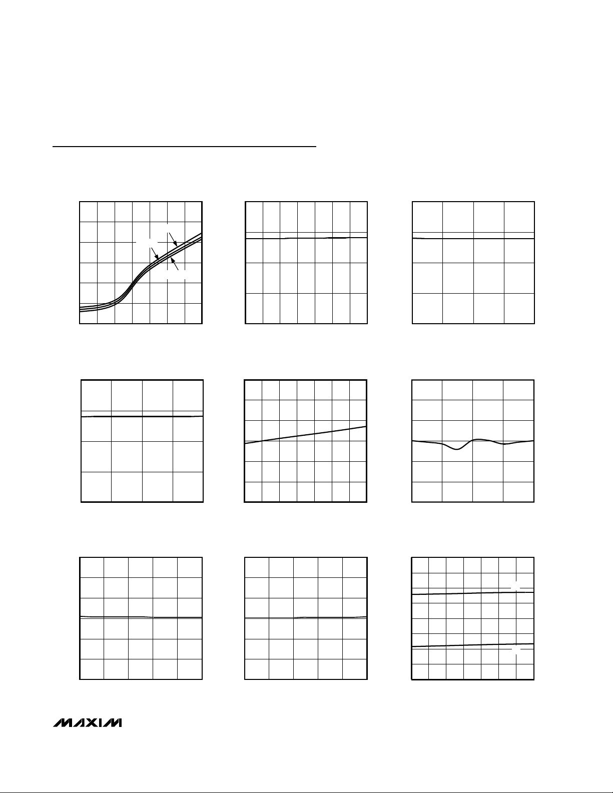
Typical Operating Characteristics
(VCC= +5V, VEE= -5V, TA = +25°C, unless otherwise noted.)
V.11 OR V.35 DIFFERENTIAL-MODE
IMPEDANCE vs. TEMPERATURE
106.0
105.5
105.0
104.5
IMPEDANCE (Ω)
104.0
103.5
103.0
0304010 20 50 60 70
TEMPERATURE (°C)
VCM = -7V
VCM = 0
V.11 OR V.35 DIFFERENTIAL-MODE
IMPEDANCE vs. SUPPLY VOLTAGE (V
110
105
VCM = +7V
EE
MXL1344A toc01
)
MXL1344A toc04
V.11 OR V.35 DIFFERENTIAL-MODE
IMPEDANCE vs. COMMON MODE VOLTAGE
110
105
100
IMPEDANCE (Ω)
95
90
-7 -1 1-5 -3 3 5 7
V.35 COMMON-MODE IMPEDANCE
165
160
155
VCM (V)
vs. TEMPERATURE
MXL1344A toc02
MXL1344A toc05
V.11 OR V.35 DIFFERENTIAL-MODE
IMPEDANCE vs. SUPPLY VOLTAGE (V
110
105
100
IMPEDANCE (Ω)
95
90
4.50 5.004.75 5.25 5.50
VCC (V)
V.35 COMMON-MODE IMPEDANCE
vs. COMMON-MODE VOLTAGE (V
165
160
155
CM
CC
)
)
MXL1344A toc03
MXL1344A toc06
100
IMPEDANCE (Ω)
95
90
-5.50 -5.00-5.25 -4.75 -4.50
VEE (V)
V.35 COMMON-MODE IMPEDANCE
vs. SUPPLY VOLTAGE (V
165
160
155
150
IMPEDANCE (Ω)
145
140
135
4.5 4.94.7 5.1 5.3 5.5
VCC (V)
CC
150
IMPEDANCE (Ω)
145
140
135
0304010 20 50 60 70
TEMPERATURE (°C)
150
IMPEDANCE (Ω)
145
140
135
-2 0-1 1 2
VCM (V)
V.35 COMMON-MODE IMPEDANCE
)
165
160
MXL1344A toc07
155
150
IMPEDANCE (Ω)
145
140
135
vs. SUPPLY VOLTAGE (V
-5.5 -5.1-5.3 -4.9 -4.7 -4.5
VEE (V)
)
EE
MXL1344A toc08
SUPPLY CURRENT vs. TEMPERATURE
500
450
400
350
300
250
SUPPLY CURRENT (µA)
200
150
100
0203010
40
TEMPERATURE (°C)
I
EE
I
CC
50 60 70
MXL1344A toc09
Page 4
Detailed Description
The MXL1344A contains six software-selectable multiprotocol cable termination networks (Figure 3). Each
network is capable of terminating V.11 (RS-422, RS530, RS-530A, RS-449, V.36 and X.21) with a 100Ω differential load, V.35 with a T-network load, or V.28
(RS-232) and V.10 (RS-423) with an open-circuit load
for use with transceivers having on-chip termination.
The termination protocol can be selected by the serial
interface cable wiring or by software control. The
MXL1344A replaces discrete resistor termination net-
works and expensive relays required for multiprotocol
termination, saving space and cost.
The MXL1344A terminator is designed to form a complete +5V cable- or software-selectable multiprotocol
DTE/DCE interface port when used with the MXL1543
and MXL1544/MAX3175 transceivers. The MXL1344A
terminator can use the VEEpower generated by the
MXL1543 charge pump, simplifying system design. The
MXL1344A, MXL1543, and MXL1544/MAX3175 are pinfor-pin compatible with the LTC1344A, LTC1543, and
LTC1544, but for proper operation, the entire Maxim
MXL1344A
+5V Multiprotocol, Software-Selectable
Cable Terminator
4 _______________________________________________________________________________________
Pin Description
*V
EE
is typically supplied by the charge pump of the MXL1543. The VEEinput level varies with the mode of chipset operation
as follows:
V.35/V.28 Modes: -6.50V ≤ V
EE
≤ -5.45V, in typical operation VEE= -5.80V
V.10/V.11 Modes: -4.60V ≤ V
EE
≤ -3.80V, in typical operation VEE= -4.20V
PIN NAME FUNCTION
1 M0 Mode-Select Pin (Table 1)
2V
3 R1C Load 1, Center Tap
4 R1B Load 1, Node B
5 R1A Load 1, Node A
6 R2A Load 2, Node A
7 R2B Load 2, Node B
8 R2C Load 2, Center Tap
9 R3A Load 3, Node A
10 R3B Load 3, Node B
11 R3C Load 3, Center Tap
12, 13 GND Ground
14 V
15 R4B Load 4, Node B
16 R4A Load 4, Node A
17 R5B Load 5, Node B
18 R5A Load 5, Node A
19 R6A Load 6, Node A
20 R6B Load 6, Node B
21 LATCH
22 DCE/ DTE Logic Level HIGH selects DCE interface, (Table 1)
23 M2 Mode-Select Pin (Table 1)
24 M1 Mode-Select Pin (Table 1)
EE
CC
Negative Supply Voltage (typically connected to VEE of MXL1543*). Bypass to GND with a 0.1µF
capacitor.
+5V Supply Voltage. Bypass to GND with a 0.1µF capacitor.
Latch Signal Input. When LATCH is LOW, the input latches are transparent. When LATCH is high, the
data at the mode-select inputs are latched.
Page 5

MXL1344A
+5V Multiprotocol, Software-Selectable
Cable Terminator
_______________________________________________________________________________________ 5
Figure 1. V.11 or V.35 Differential Impedance Measurement
Figure 3. Block Diagram
Figure 2. V.35 Common-Mode Impedance Measurement
chipset must be used without substituting other manufacturer's parts on a chip-by-chip basis.
Termination Modes
The termination networks in the MXL1344A can be set
to one of three modes, V.11, V.35, or high impedance
(high-Z). As shown in Figure 4, in V.11 mode, switch S1
is closed and switch S2 is open, presenting 104Ω
across terminals A and B. In V.35 mode, switches S1
and S2 are both closed, presenting a T-network with
104Ω differential impedance and 153Ω common-mode
impedance. In high-Z mode, switches S1 and S2 are
both open, presenting a high impedance across terminals A and B suitable for V.28 and V.10 modes.
A
I
AMMETER
= ±2V
V
DM
R1 = 52Ω
S1 ON
R2 = 52Ω
B
VCM = ±7V OR ±2V
V
DM
R
=
DM
I
R3 = 127Ω
S2 OFF
A
R1 = 52Ω
S1 ON
R3 = 127Ω
S2 ON
VCM = ±2V
AMMETER
R
CM
I
R2 = 52Ω
V
CM
=
I
B
3 8 11 12 13
1
M0
M1
M2
DCE/DTE
LATCH
V
CCVEE
MXL1344A
12 34 56
52
4 6 7 9 10 16 15 18 1714 19 20
24
23
22
21
Page 6

MXL1344A
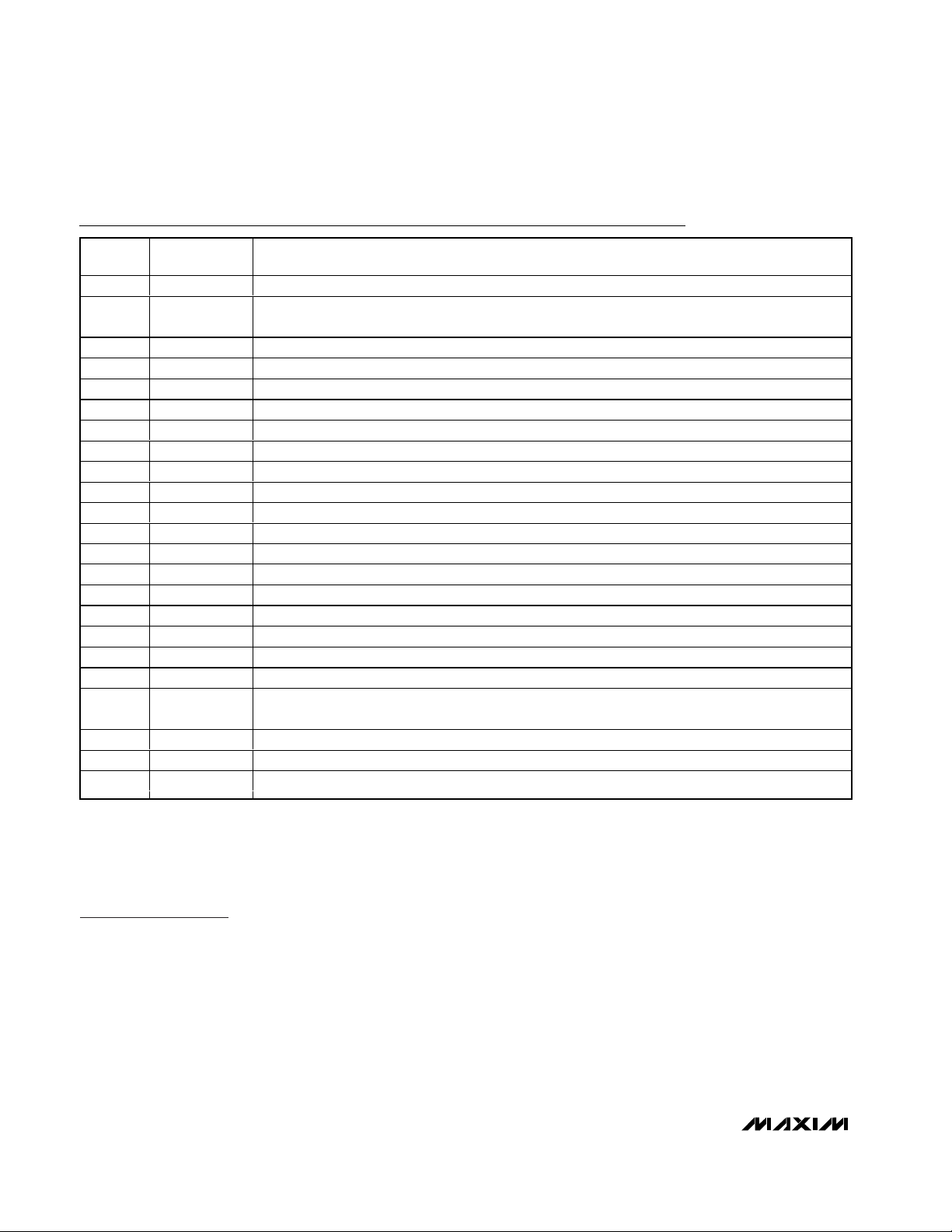
The state of the MXL1344A’s mode-select pins, M0,
M1, M2, and DCE/DTE determines the mode of each of
the six termination networks. Table 1 shows a cross-ref-
erence of termination mode and select pin state for
each of the six termination networks within the
MXL1344A.
+5V Multiprotocol, Software-Selectable
Cable Terminator
6 _______________________________________________________________________________________
Table 1. Termination Mode Select Table
Note: Z Indicates high impedance, 1 = high and 0 = low. Z, V.11, and V.35 refer to termination modes (Figure 4.)
Figure 4. Termination Modes
A
MXL1344A
R1
52Ω
S1
CLOSED
A
MXL1344A MXL1344A
R1
52Ω
S1
CLOSED
C
A
R1
52Ω
S1
OPEN
CC
S2
OPEN
R2
52Ω
B
R3
127Ω
B
(a) V.11 (b) V.35 (c) Z
PROTOCOL DCE/ DTE M2 M1 M0 R1 R2 R3 R4 R5 R6
V.10/RS-423 0 0 0 0 Z Z Z Z Z Z
RS-530A 0 0 0 1 Z Z Z V.11 V.11 V.11
RS-530 0 0 1 0 Z Z Z V.11 V.11 V.11
X.21 0 0 1 1 Z Z Z V.11 V.11 V.11
V.35 0 1 0 0 V.35 V.35 Z V.35 V.35 V.35
RS-449/V.36 0 1 0 1 Z Z Z V.11 V.11 V.11
V.28/RS-232 0 1 1 0 Z Z Z Z Z Z
No Cable 0 1 1 1 V.11 V.11 V.11 V.11 V.11 V.11
V.10/RS-423 1 0 0 0 Z Z Z Z Z Z
RS-530A 1 0 0 1 Z Z Z Z V.11 V.11
RS-530 1 0 1 0 Z Z Z Z V.11 V.11
X.21 1 0 1 1 Z Z Z Z V.11 V.11
V.35 1 1 0 0 V.35 V.35 V.35 Z V.35 V.35
RS-449/V.36 1 1 0 1 Z Z Z Z V.11 V.11
V.28/RS-232 1 1 1 0 Z Z Z Z Z Z
No Cable 1 1 1 1 V.11 V.11 V.11 V.11 V.11 V.11
S2
CLOSED
R2
52Ω
R3
127Ω
S2
OPEN
R2
52Ω
B
R3
127Ω
Page 7
MXL1344A
+5V Multiprotocol, Software-Selectable
Cable Terminator
_______________________________________________________________________________________ 7
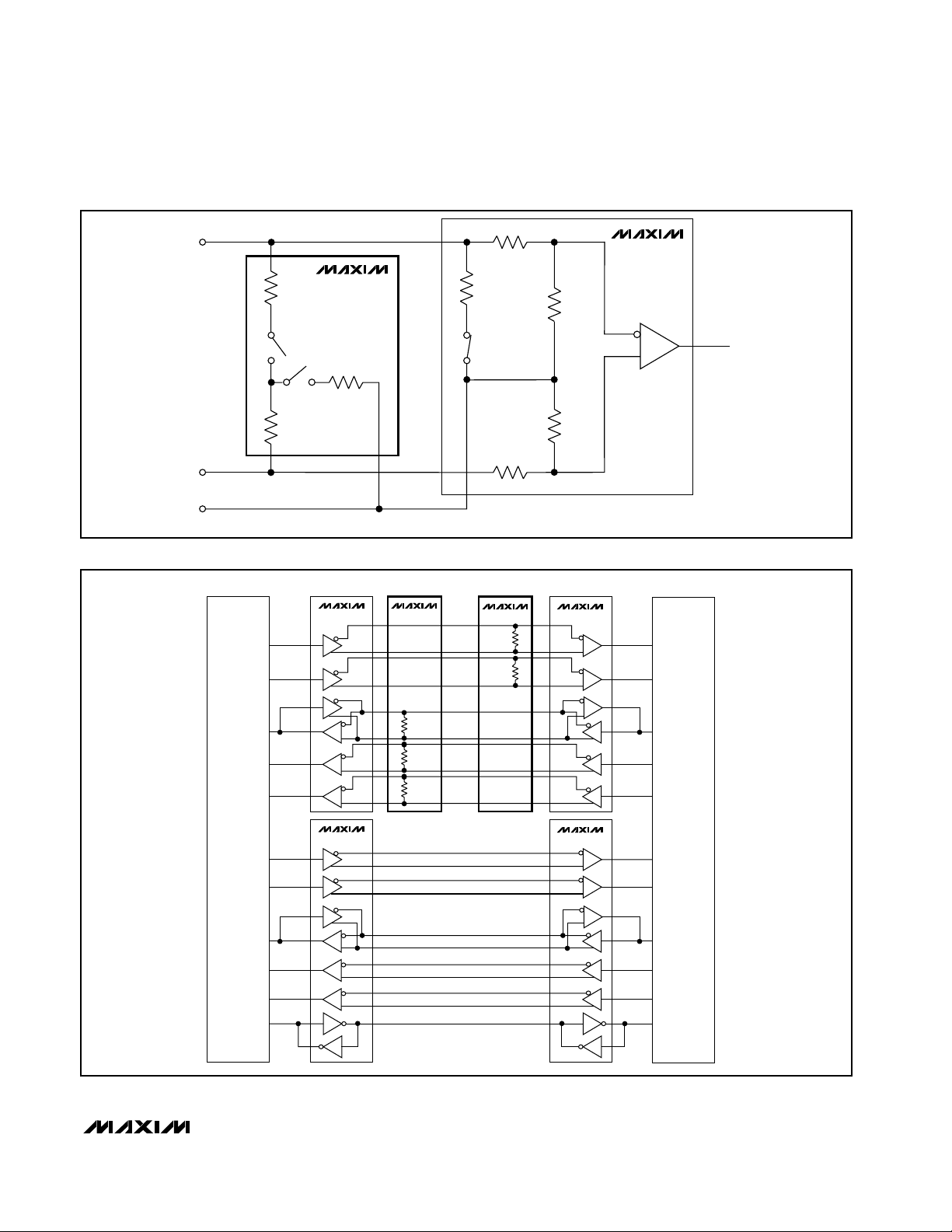
Figure 5. Cable-Selectable Multiprotocol DCE/DTE Serial Interface (Configured in RS-530A DTE Mode)
DTE_TXD/DCE_RXD
DTE_SCTE/DCE_RXC
DTE_TXC/DCE_TXC
DTE_RXC/DCE_SCTE
DTE_RXD/DCE_TXD
100pF 100pF100pF
3 8 11 12 13
V
4.7µF
CC
5V
CHARGE
PUMP
D1
D2
D3
R1
R2
R3
MXL1543
28
1µF
27
26
4.7µF
25
24
23
22
21
20
19
18
17
16
15
3
1
1µF
2
1µF
5
6
7
8
9
10
11
M0
12
M1
13
M2
14
DCE/DTE
0.1µF
14
2
54 67 910161518171920 2223241
0.1µF
MXL1344A
DCE/DTE
M2
LATCH
M1
21
SYSTEM
PROPRIETARY
S GND
CONNECTOR
INTERCONNECT
CABLE
2
14
24
11
15
12
17
9
3
16
7
1
TXD A
TXD B
SCTE A
SCTE B
TXC A
TXC B
RXC A
RXC B
RXD A
RXD B
SIGNAL GND
SHIELD
M0
DB-25
CONNECTOR
DTE
RXD A
RXD B
RXC A
RXC B
SCTE A
SCTE B
DCE
TXC A
TXC B
TXD A
TXD B
V
DTE_RTS/DCE_CTS
DTE_DTR/DCE_DSR
DTE_DCD/DCE_DCD
DTE_DSR/DCE_DTR
DTE_CTS/DCE_RTS
LOCAL_LOOP_BACK
CC
0.1µF
1µF
1
V
CC
2
V
DD
3
4
5
6
7
8
10
9
11
M0
12
M1
13
M2
14
DCE/DTE INVERT
D1
D2
D3
R1
R2
R3
R4
D4
MXL1544/
MAX3175
GND
28
V
EE
27
26
25
24
23
22
21
20
19
18
17
16
15
0.1µF
M0
M1
M2
DCE/DTE
4
CTS A
RTS A
19
RTS B
CTS B
20
DSR A
DTR A
23
DTR B
DSR B
8
DCD A
DCD A
10
DCD B
DCD B
6
DTR A
DSR A
22
DTR B
DSR B
5
RTS A
CTS A
13
RTS B
CTS B
18
LL
Page 8

MXL1344A
+5V Multiprotocol, Software-Selectable
Cable Terminator
8 _______________________________________________________________________________________
No-Cable Mode
The MXL1344A enters no-cable mode when the mode
select inputs, M0, M1, and M2 are connected HIGH or
left unconnected. In no-cable mode, all six termination
networks are placed in V.11 mode, with S1 closed and
S2 open (Figure 4).
Applications Information
Older multiprotocol interface termination circuits have
been constructed using expensive relays with discrete
resistors, custom cables with built-in termination, or
complex circuit-board configurations to route signals to
the correct termination. The MXL1344A provides a simple solution to this termination problem. All required termination configurations are easily cable- or softwareselectable using the four mode-control input pins M0,
M1, M2, and DCE/DTE.
Using the MXL1344A in a Multiprotocol
Serial Interface
The MXL1344A terminator is designed to form a complete +5V cable- or software-selectable multiprotocol
DCE/DTE interface port when used with the MXL1543
and MXL1544/MAX3175 differential driver/receivers.
The MXL1344A terminator is designed to use the V
EE
power generated by the MXL1543’s charge pump and
will meet all data sheet specifications when connected
as illustrated in Figure 5. The mode-selection tables of
all three devices are identical, allowing the M0, M1, M2,
and DCE/DTE pins of each device to be connected to a
single 4-wire control bus. The MXL1543 and MXL1544/
MAX3175 provide internal pullups for the four lines,
forcing them to the logic high state if they are not
grounded. This allows interface-mode configuration by
simply strapping the appropriate pins to ground in the
interconnect cable.
In Figure 5, M1, M2 and DCE/DTE are shorted to the
cable ground, forcing logic LOW on these control lines.
Input M0 is left floating and will be pulled HIGH by
internal pullups on the MXL1543 and MXL1544/
Figure 6. Typical V.11 Interface
Figure 7. V.11 Termination and Internal Resistance Networks
BALANCED
INTERCONNECTING
GENERATOR
CABLE
TERMINATION
A
B
C
A′
B′
C′
LOAD
CABLE
RECEIVER
100Ω
MIN
A′
R1
52Ω
S1
R2
52Ω
B′
C′
MXL1344A
R3
127Ω
S2
A
R5
30kΩ
R8
5kΩ
S3
B
GND
R6
10kΩ
R7
10kΩ
R4
30kΩ
MXL1543
RECEIVER
Page 9

MAX3175. With this cable wiring, the multiprotocol serial port is set in RS-530A DTE mode (Table 1).
V.11 Termination
A standard V.11 interface is shown in Figure 6. For
high-speed data transmission, the V.11 specification
recommends terminating the cable at the receiver with
a 100Ω (min) resistor. The resistor, although not
required, prevents reflections from corrupting transmitted data.
In Figure 7, the MXL1344A is used to terminate the V.11
receiver on the MXL1543. Internal to the MXL1344A, S1
is closed and S2 is open to present a 104Ω typical differential resistance and high-Z common-mode impedance. The MXL1543's internal V.28 termination is
disabled by opening S3.
The V.11 specification allows for signals with commonmode variations of ±7V and differential signal amplitudes from 2V to 6V with data rates as high as 10Mbps.
The MXL1344A maintains termination impedance
between 100Ω and 110Ω over these conditions.
V.35 Termination
Figure 8 shows a standard V.35 interface. The generator and the load must both present a 100Ω ±10Ω differ-
ential impedance and a 150Ω ±15Ω common-mode
impedance. The V.35 driver generates a current output
(±11mA typ) that develops an output voltage between
440mV and 660mV across the load termination networks.
In Figure 9, the MXL1344A is used to implement the
resistive T-network that is needed to properly terminate
MXL1344A
+5V Multiprotocol, Software-Selectable
Cable Terminator
_______________________________________________________________________________________ 9
Figure 8. Typical V.35 Interface
Figure 9. V.35 Termination and Internal Resistance Networks
A′
B′
GENERATOR
50Ω
50Ω
S1
R1
52Ω
R2
52Ω
125Ω
S2
MXL1344A
R3
127Ω
A
B
C
BALANCED
INTERCONNECTING
CABLE
A
R8
5kΩ
S3
B
R5
30kΩ
R4
30kΩ
A′
B′
C′
10kΩ
10kΩ
R6
R7
CABLE
TERMINATION
125Ω
LOAD
RECEIVER
50Ω
50Ω
MXL1543
RECEIVER
C′
GND
Page 10

MXL1344A
the V.35 receiver. Internal to the MXL1344A, S1 and S2
are closed to connect the T-network resistors to the circuit.
The V.35 specification allows for ±4V of ground difference
between the V.35 generator and V.35 load, with data
rates as high as 10Mbps. The MXL1344A maintains correct termination impedance over these conditions.
V.35 EMI reduction
For applications where EMI reduction is especially
important, the MXL1344A termination networks provide
a pin for shunting common-mode driver currents to
GND. Mismatches between the driver A and B output
propagation delays can create a common-mode disturbance on the cable. This common-mode energy can be
shunted to GND by placing a 100pF capacitor to GND
from the center tap of the T-network termination (R1C,
R2C and R3C as shown in Figure 5).
V.28 Termination
Most industry-standard V.28 receivers (including the
MXL1543) do not require external termination because
the receiver includes an internal 5kΩ termination resistor. When the MXL1344A is placed in V.28 mode, all six
of the termination networks are placed in a high-Z
mode. In high-Z mode, the MXL1344A termination networks will not interfere with the MXL1543's internal 5kΩ
termination.
In Figure 10, the MXL1344A and MXL1543 are placed
in V.28 mode. Switches S1 and S2 are opened on the
MXL1344A to place the network in high-Z mode. Switch
S3 is closed on the MXL1543 to enable the 5kΩ termi-
nating resistor.
A Complete X.21 Interface
A complete DTE-to-DCE interface operating in X.21
mode is shown in Figure 11. The MXL1344A terminates
the V.11 clock and data signals. The MXL1543 carries
the clock and data signals, and the MXL1544/MAX3175
carries the control signals. The control signals generally
do not require external termination.
Compliance Testing
A European Standard EN 45001 test report for the
MXL1543, MXL1544/MAX3175, and MXL1344A chipset
will be available from Maxim upon completion of testing. Contact Maxim Quality Assurance for a copy of the
report.
Chip Information
TRANSISTOR COUNT: 1,054
PROCESS TECHNOLOGY: BiCMOS
+5V Multiprotocol, Software-Selectable
Cable Terminator
10 ______________________________________________________________________________________
Pin Configuration
TOP VIEW
M0
V
R1C
R1B
R1A
R2A
R2B
R3A
R3B
R3C
GND
1
2
EE
3
4
MAX1344A
5
6
7
8
9
10
11
12
24 SSOP
24
23
22
21
20
19
18
17
16
15
14
13
M1
M2
DCE/DTE
LATCH
R6B
R6A
R5A
R5BR2C
R4A
R4B
V
CC
GND
Page 11
MXL1344A
+5V Multiprotocol, Software-Selectable
Cable Terminator
______________________________________________________________________________________ 11
Figure 10. V.28 Termination and Internal Resistance Networks
Figure 11. DTE-to-DCE X.21 Interface
A′
R1
52Ω
S1
MXL1344A
R3
127Ω
S2
R2
52Ω
B′
C′
DTE
SERIAL
CONTROLLER
SCTE
TXD
D1
D2
MXL1344AMXL1543
A
MXL1543
RECEIVER
R8
5kΩ
R5
30kΩ
10kΩ
R6
S3
R7
10kΩ
R4
B
30kΩ
GND
DCE
SERIAL
CONTROLLER
TXD
SCTE
TXD
SCTE
104Ω
104Ω
MXL1543MXL1344A
R3
R2
TXC
RXC
RXD
RTS
DTR
DCD
DSR
CTS
LL
D3
R1
R2
R3
MXL1544/MAX3175
D1
D2
D3
R1
R2
R3
D4
R4
104Ω
104Ω
104Ω
TXC
RXC
RXD
RTS
DTR
DCD
DSR
CTS
R1
D3
D2
D1
MXL1544/MAX3175
R3
R2
R1
D3
D2
D1
LL
R4
D4
TXC
RXC
RXD
RTS
DTR
DCD
DSR
CTS
LL
Page 12

MXL1344A
+5V Multiprotocol, Software-Selectable
Cable Terminator
Maxim cannot assume responsibility for use of any circuitry other than circuitry entirely embodied in a Maxim product. No circuit patent licenses are
implied. Maxim reserves the right to change the circuitry and specifications without notice at any time.
12 ____________________Maxim Integrated Products, 120 San Gabriel Drive, Sunnyvale, CA 94086 408-737-7600
© 2001 Maxim Integrated Products Printed USA is a registered trademark of Maxim Integrated Products.
Package Information
SSOP.EPS
 Loading...