

Maxim MXD1013C-D040, MXD1013C-D045, MXD1013C-D050, MXD1013C-D060, MXD1013C-D070 Datasheet
...
_______________General Description
The MXD1013 contains three independent, monolithic,
logic-buffered delay lines with delays ranging from
10ns to 200ns. Nominal accuracy is ±2ns for a 10ns to
60ns delay, ±3% for a 70ns to 100ns delay, and ±5%
for a 150ns to 200ns delay. Relative to hybrid solutions,
these devices offer enhanced performance and higher
reliability, and reduce overall cost. Each output can
drive up to ten standard 74LS loads.
The MXD1013 is available in multiple versions, each
offering a different combination of delay times. It comes
in the space-saving 8-pin µMAX package, as well as a
standard 8-pin SO and DIP. It is also offered in industry-standard 16-pin SO and 14-pin DIP packaging,
allowing full compatibility with the DS1013 and other
delay-line products.
________________________Applications
Clock Synchronization
Digital Systems
____________________________Features
♦ Improved Second Source to DS1013
♦ Available in Space-Saving 8-Pin µMAX Package
♦ 20mA Supply Current (vs. Dallas’ 40mA)
♦ Low Cost
♦ Three Separate Buffered Delays
♦ Delay Tolerance of ±2ns for MXD1013__010
through MXD1013__060
♦ TTL/CMOS-Compatible Logic
♦ Leading- and Trailing-Edge Accuracy
♦ Custom Delays Available
MXD1013
3-in-1 Silicon Delay Line
________________________________________________________________
Maxim Integrated Products
1
OUT2
OUT3GND
1
2
87V
CC
OUT1IN2
IN3
IN1
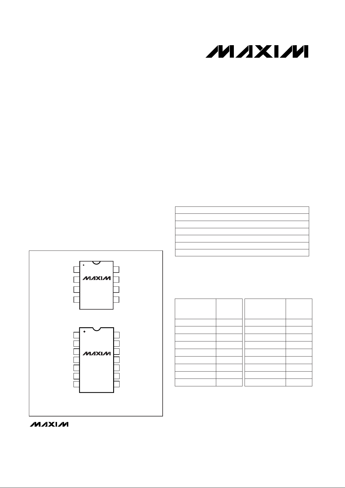
DIP/SO/µMAX
TOP VIEW
3
4
6
5
MXD1013
14
13
12
11
10
9
8
1
2
3
4
5
6
7
V
CC
N.C.
OUT1
N.C.N.C.
IN2
N.C.
IN
MXD1013
OUT2
N.C.
OUT3GND
N.C.
IN3
DIP
_________________Pin Configurations
19-0394; Rev 0; 12/97
*
Dice are tested at TA= +25°C.
Note: To complete the ordering information, fill in the blank with
the part number extension from the Part Numbers and Delay
Times table to indicate the desired delay per output.
For free samples & the latest literature: http://www.maxim-ic.com, or phone 1-800-998-8800.
For small orders, phone 408-737-7600 ext. 3468.
PART
MXD1013C/D___
MXD1013PA___
MXD1013PD___ -40°C to +85°C
-40°C to +85°C
0°C to +70°C
TEMP. RANGE PIN-PACKAGE
Dice*
8 Plastic DIP
14 Plastic DIP
MXD1013SA___
MXD1013SE___
MXD1013UA___ -40°C to +85°C
-40°C to +85°C
-40°C to +85°C 8 SO
16 Narrow SO
8 µMAX
______________Ordering Information
___Part Numbers and Delay Times
Pin Configurations continued at end of data sheet.
Functional Diagram appears at end of data sheet.
OUTPUT
DELAY
(ns)
070
050 50
70
080
075 75
80
100
090 90
100
PART NUMBER
EXTENSION
(MXD1013___)
150 150
012
OUTPUT
DELAY
(ns)
010 10
12
020
015 15
20
030
025 25
30
040
035 35
40
PART NUMBER
EXTENSION
(MXD1013___)
045 45
200 200
060 60
MXD1013
3-in-1 Silicon Delay Line
2 _______________________________________________________________________________________
ABSOLUTE MAXIMUM RATINGS
ELECTRICAL CHARACTERISTICS
(VCC= +5.0V ±5%, TA= -40°C to +85°C, unless otherwise noted. Typical values are at TA= +25°C.)(Note 1)
TIMING CHARACTERISTICS
(VCC= +5.0V ±5%, TA= +25°C, unless otherwise noted.)
Stresses beyond those listed under “Absolute Maximum Ratings” may cause permanent damage to the device. These are stress ratings only, and functional
operation of the device at these or any other conditions beyond those indicated in the operational sections of the specifications is not implied. Exposure to
absolute maximum rating conditions for extended periods may affect device reliability.
Note 1: Specifications to -40°C are guaranteed by design, not production tested.
Note 2: All voltages referenced to GND.
Note 3: Measured with outputs open.
Note 4: Guaranteed by design.
Note 5: Pulse width and/or period specifications may be exceeded, but accuracy is application sensitive (i.e., layout, decoupling, etc.).
Note 6: V
CC
= +5V at +25°C. Typical delays are accurate on both rising and falling edges within ±2ns for delays from 10ns to
60ns, within ±3% for delays from 70ns to 100ns, and within ±5% for delays from 150ns to 200ns.
Note 7: The
Part Number and Delay Times
table provides typical delays at +25°C with VCC= +5V. The delays may shift with temperature and supply variations. The combination of temperature (from +25°C to 0°C, or +25°C to +70°C) and supply variation (from 5V to 4.75V, or 5V to 5.25V) could produce an additional typical delay of ±1.5ns or ±3%, whichever is greater.
Note 8: All output delays tend to vary unidirectionally with temperature or supply voltage variations (i.e., if OUT1 slows down, all
other outputs also slow down).
V
CC
to GND..............................................................-0.5V to +6V
All Other Pins..............................................-0.5V to (V
CC
+ 0.5V)
Short-Circuit Output Current (1sec)....................................50mA
Continuous Power Dissipation (T
A
= +70°C)
8-Pin Plastic DIP (derate 9.1mW/°C above +70°C) .......727mW
14-Pin Plastic DIP (derate 10.0mW/°C above +70°C) ...800mW
8-Pin SO (derate 5.9mW/°C above +70°C)....................471mW
16-Pin Narrow SO (derate 8.7mW/°C above +70°C).....696mW
8-Pin µMAX (derate 4.1mW/°C above +70°C)...............330mW
Operating Temperature Range ...........................-40°C to +85°C
Storage Temperature Range.............................-65°C to +160°C
Lead Temperature (soldering, 10sec).............................+300°C
(Note 2)
(Note 2)
(Note 2)
TA= +25°C (Note 4)
0V ≤ VIN≤ V
CC
VCC= 5.25V, period = minimum (Note 3)
VCC= 4.75V, VOH= 4.0V
VCC= 4.75V, VOL= 0.5V
CONDITIONS
V0.8V
IL
Input Voltage Low
V2.2V
IH
V4.75 5.00 5.25V
CC
Supply Voltage
Input Voltage High
pF5 10C
IN
Input Capacitance
µA-1 1I
L
Input Leakage Current
mA20 70I
CC
Active Current
mA-1I
OH
Output Current High
mA12I
OL
Output Current Low
UNITSMIN TYP MAXSYMBOLPARAMETER
(Notes 6, 7, 8)
(Notes 6, 7, 8)
(Note 5)
(Note 5)
CONDITIONS
ns
See Part Number and
Delay Times table
t
PHL
Input-to-Output Delay
(trailing edge)
ns
See Part Number and
Delay Times table
t
PLH
ns100% of t
PLH
t
WI
Input Pulse Width
Input-to-Output Delay
(leading edge)
ms100t
PU
Power-Up Time
ns3(tWI)Period
UNITSMIN TYP MAXSYMBOLPARAMETER

MXD1013
3-in-1 Silicon Delay Line
_______________________________________________________________________________________
3
__________________________________________Typical Operating Characteristics
(VCC= +5V, TA= +25°C, unless otherwise noted.)
11.0
10.5
6.0
0.0001 0.1 1 100.010.001 100
ACTIVE CURRENT
vs. INPUT FREQUENCY
7.0
6.5
MXD1013 TOC01
INPUT FREQUENCY (MHz)
ACTIVE CURRENT (mA)
8.0
7.5
9.0
8.5
10.0
9.5
ALL INPUTS CONNECTED TOGETHER
0V–3V INPUT
NO LOAD
MXD1013_ _030
MXD1013_ _075
-2.0
-1.0
-1.5
0
-0.5
1.5
1.0
0.5
2.0
-40 0-20 20 40 60 80 100
MXD1013_ _100
PERCENT CHANGE IN DELAY
vs. TEMPERATURE (OUT1)
MXD1013 TOC2
TEMPERATURE (°C)
% CHANGE IN DELAY
t
PHL
t
PHL
t
PLH
t
PLH
-2.0
-1.0
-1.5
0
-0.5
1.5
1.0
0.5
2.0
-40 0-20 20 40 60 80 100
MXD1013_ _100
PERCENT CHANGE IN DELAY
vs. TEMPERATURE (OUT2)
MXD1013 TOC3
TEMPERATURE (°C)
% CHANGE IN DELAY
t
PHL
t
PHL
t
PLH
t
PLH
-2.0
-1.0
-1.5
0
-0.5
1.5
1.0
0.5
2.0
-40 0-20 20 40 60 80 100
MXD1013_ _00
PERCENT CHANGE IN DELAY
vs. TEMPERATURE (OUT3)
MXD1013 TOC4
TEMPERATURE (°C)
% CHANGE IN DELAY
t
PHL
t
PHL
t
PHL
t
PLH
t
PLH
t
PLH

_______________Definitions of Terms
Period: The time elapsed between the first pulse’s
leading edge and the following pulse’s leading edge.
Pulse Width (tWI): The time elapsed on the pulse
between the 1.5V level on the leading edge and the
1.5V level on the trailing edge, or vice versa.
Input Rise Time (t
RISE
): The elapsed time between
the 20% and 80% points on the input pulse’s leading
edge.
Input Fall Time (t
FALL
): The time elapsed between
the 80% and 20% points on the input pulse’s trailing
edge.
Time Delay, Rising (t
PLH
): The time elapsed between
the 1.5V level on the input pulse’s leading edge and the
corresponding output pulse’s leading edge.
Time Delay, Falling (t
PHL
): The time elapsed between
the 1.5V level on the input pulse’s trailing edge and the
corresponding output pulse’s trailing edge.
____________________Test Conditions
Ambient Temperature: +25°C
Supply Voltage (VCC): 5.0V ±0.1V
Input Pulse: High = 3.0V ±0.1V
Low = 0.0V ±0.1V
Source Impedance: 50Ω max
Rise and Fall Times: 3.0ns max
Pulse Width: 500ns max
Period: 1µs
Each output is loaded with a 74F04 input gate. Delay is
measured at the 1.5V level on the rising and falling
edges. The time delay due to the 74F04 is subtracted
from the measured delay.
MXD1013
3-in-1 Silicon Delay Line
4 _______________________________________________________________________________________
______________________________________________________________Pin Description
1 1 First Independent Input
14-PIN DIP
FUNCTION
8-PIN
DIP/SO/µMAX
NAME
16-PIN SO
2 3 Second Independent Input4
1 IN1
IN2
3
PIN
5 Third Independent Input
4 7 Device Ground8
6 IN3
GND
5 8 Third Delayed Output
6 10 Second Delayed Output11
9 OUT3
OUT2
7 12 First Delayed Output
8 14 Power-Supply Input16
13 OUT1
V
CC
—
2, 4, 6, 9, 11,
13
Not Connected
2, 3, 5, 7, 10,
12, 14, 15
N.C.

__________ Applications Information
Supply and Temperature
Effects on Delay
Over the specified range, the MXD1013’s delays are
typically 2% accurate. Variations in supply voltage may
affect the MXD1013’s fixed output delays. Supply voltages beyond the specified range may result with larger
variations. Although there might be a slight variance in
delays over temperature, the MXD1013 is internally
compensated to maintain its nominal values.
Loading Effect on Delay Lines
Capacitive loads increase delay times as they increase
the rise and fall times of the delay lines. Other logic
devices increase the capacitance at the output of the
delays, which can affect device performance.
Board Layout Considerations
Bypass the MXD1013 with a 0.1µF capacitor to minimize the impact of high-speed switching on the power
supply. The power supply must be able to deliver the
required switching currents for proper operation.
It is advisable to minimize trace lengths in order to
reduce board capacitance as well as the traveling distance between devices. Sockets and wire-wrapped
boards increase capacitance and should be avoided.
MXD1013
3-in-1 Silicon Delay Line
_______________________________________________________________________________________ 5
Figure 1. Timing Diagram
MXD1013
TD
74F04
50Ω
50Ω
50Ω
74F04
74F04
PULSE
GENERATOR
TD
PULSE
GENERATOR
TD
PULSE
GENERATOR
EACH OUTPUT IS LOADED WITH THE EQUIVALENT OF ONE 74F04.
THE DELAY OF THE 74F04 IS SUBTRACTED FROM THE MEASURED DELAY.
TIME
INTERVAL
COUNTER
Figure 2. Test Circuit
V
IL
V
IH
PERIOD
t
RISE
IN
OUT
0.6V
0.6V
2.4V
2.4V
1.5V
1.5V 1.5V
1.5V
1.5V
t
FALL
t
WI
t
PLH
t
PHL
___________________Chip Information
TRANSISTOR COUNT: 824

Maxim cannot assume responsibility for use of any circuitry other than circuitry entirely embodied in a Maxim product. No circuit patent licenses are
implied. Maxim reserves the right to change the circuitry and specifications without notice at any time.
6
_____________________Maxim Integrated Products, 120 San Gabriel Drive, Sunnyvale, CA 94086 408-737-7600
© 1997 Maxim Integrated Products Printed USA is a registered trademark of Maxim Integrated Products.
MXD1013
3-in-1 Silicon Delay Line
MXD1013
TD OUT1
TD
OUT2
TD
OUT3
IN1
IN2
IN3
________________Functional Diagram
________________________________________________________Package Information
8LUMAXD.EPS
TOP VIEW
16
15
14
13
12
11
10
9
1
2
3
4
5
6
7
8
IN V
CC
N.C.
N.C.
OUT1
N.C.
OUT2
N.C.
OUT3
MXD1013
SO
N.C.
N.C.
IN3
IN2
N.C.
N.C.
GND
____Pin Configurations (continued)
 Loading...