19-0255; Rev 2; 4/94
CMOS, High-Speed, 8-Bit ADCs
with Multiplexer
_______________General Description
The MAX154/MAX158 and MX7824/MX7828 are highspeed, multi-channel analog-to-digital converters
(ADCs). The MAX154 and MX7824 have four analog
input channels, while the MAX158 and MX7828 have
eight channels. Conversion time for all devices is 2.5µs.
The MAX154/MAX158 also feature a 2.5V on-chip reference, forming a complete high-speed data acquisition
system.
All four converters include a built-in track/hold, eliminating the need for an external track/hold with many input
signals. The analog input range is 0V to +5V, although
the ADC operates from a single +5V supply.
Microprocessor interfaces are simplified by the ADC’s
ability to appear as a memory location or I/O port without
the need for external logic. The data outputs use latched,
three-state buffer circuitry to allow direct connection to a
microprocessor data bus or system input port.
The MX7824 and MX7828 are pin compatible with
Analog Devices’ AD7824 and AD7828. The MAX154
and MAX158, which feature internal references, are also
compatible with these products.
________________________Applications
Digital Signal Processing
High-Speed Data Acquisition
Telecommunications
High-Speed Servo Control
Audio Instrumentation
____________________________Features
♦ One-Chip Data Acquisition System
♦ Four or Eight Analog Input Channels
♦ 2.5µs per Channel Conversion Time
♦ Internal 2.5V Reference (MAX154/MAX158 only)
♦ Built-In Track/Hold Function
1
LSB Error Specification
/
♦
2
♦ Single +5V Supply Operation
♦ No External Clock
♦ New Space-Saving SSOP Package
______________Ordering Information
PART
MX7824LN
MX7824KN
MX7824LCWG 0°C to +70°C
MX7824KCWG
MX7824LCAG
MX7824KCAG 0°C to +70°C
TEMP. RANGE PIN-PACKAGE
0°C to +70°C
0°C to +70°C
24 Narrow
Plastic DIP
24 Narrow
Plastic DIP
24 Wide SO
0°C to +70°C 24 Wide SO
0°C to +70°C
24 SSOP
24 SSOP
Ordering Information continued on last page.
ERROR
(LSB)
1
±
/
±1
1
±
/
±1
1
/
±
±1
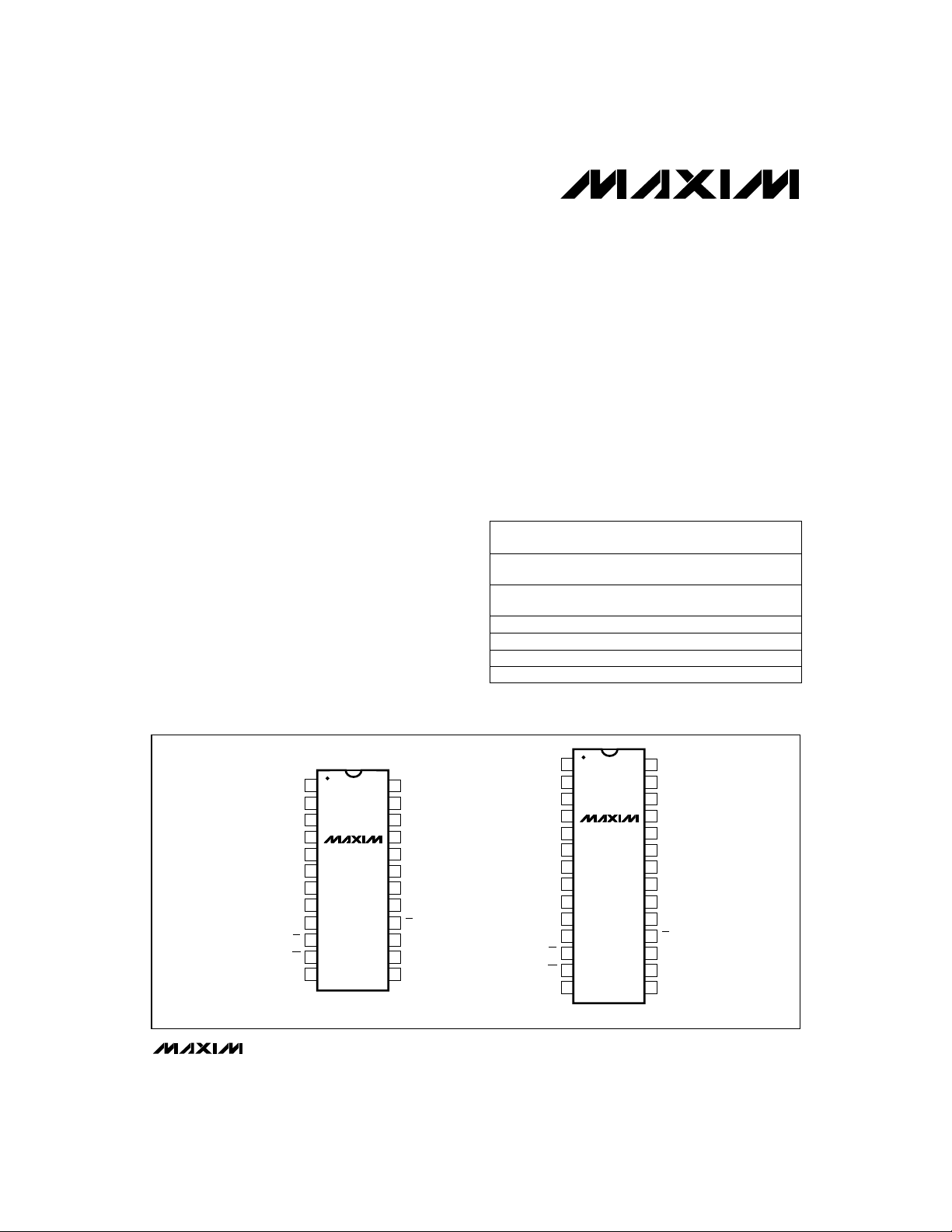
__________________________________________________________Pin Configurations
MX7824/MX7828
2
2
2
TOP VIEW
AIN4
1
AIN3
2
AIN2
3
AIN1
4
TP (REF OUT)
DB0
DB1
DB2
DB3
GND
( ) ARE FOR MAX154/MAX158 ONLY.
5
6
7
8
9
RD
10
INT
11
12
MAX154
MX7824
DIP/SO/SSOP
V
DD
24
NC
23
A0
22
A1
21
DB7
20
DB6
19
DB5
18
DB4
17
CS
16
RDY
15
+
V
14
REF
V
-
13
REF
________________________________________________________________
AIN6
AIN5
AIN4
AIN3
AIN2
AIN1
TP (REF OUT)
DB0
DB1
DB2
DB3
GND
1
2
3
4
5
6
7
8
9
10
11
RD
12
INT
13
14
MAX158
MX7828
DIP/SO/SSOP
Maxim Integrated Products
Call toll free 1-800-998-8800 for free samples or literature.
AIN7
28
AIN8
27
V
26
DD
A0
25
A1
24
A2
23
DB7
22
DB6
21
DB5
20
DB4
19
CS
18
RDY
17
V
+
16
REF
V
-
15
REF
1

CMOS, High-Speed, 8-Bit ADCs
with Multiplexer
ABSOLUTE MAXIMUM RATINGS
Supply Voltage, VDD to GND........................................0V, +10V
Voltage at Any Other Pins......................GND - 0.3V, V
Output Current (REF OUT)..................................................30mA
Power Dissipation (any package) to +75°C ....................450mW
Derate above +25°C by..............................................6mW/°C
Stresses beyond those listed under “Absolute Maximum Ratings” may cause permanent damage to the device. These are stress ratings only, and functional
operation of the device at these or any other conditions beyond those indicated in the operational sections of the specifications is not implied. Exposure to
absolute maximum rating conditions for extended periods may affect device reliability.
DD
+ 0.3V
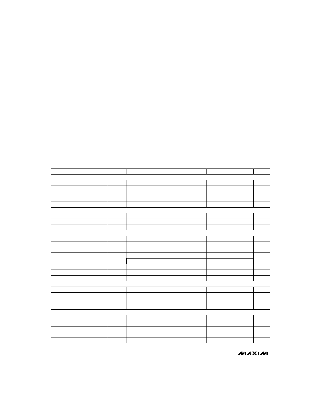
ELECTRICAL CHARACTERISTICS
(VDD= +5V, V
MX7824/MX7828
ACCURACY
Resolution 8 Bits
Total Unadjusted Error (Note 1)
No Missing Codes Resolution 8 Bits
Channel to Channel Mismatch ±1/4 LSB
REFERENCE INPUT
Reference Resistance 14kΩ
V
+ Input Voltage Range V
REF
V
- Input Voltage Range GND V
REF
REFERENCE OUTPUT—MAX154/MAX158 Only (Note 2)
Output Voltage REF OUT 2.47 2.50 2.53 V
Load Regulation -6 -10 mV
Power-Supply Sensitivity ±1 ±3 mV
Output Noise e
Capacitive Load 0.01 µF
ANALOG INPUT
Analog Input Voltage Range A
Analog Input Capacitance C
Analog Input Current I
Slew Rate, Tracking SR 0.7 0.157 V/µs
LOGIC INPUTS (–R—D–, –C—S–, A0, A1, A2)
Input High Voltage V
Input Low Voltage V
Input High Current I
Input Low Current I
Input Capacitance (Note 4) C
+ = +5V, V
REF
PARAMETER SYMBOL MIN TYP MAX UNITS
- = GND, Mode 0, TA= T
REF
N
INR
AIN
AIN
INH
INL
INH
INL
IN
MIN
MAX15_A, MX782_L/C/U
TA= +25°C
IL= 0mA to 10mA, TA= +25°C
VDD±5%, TA= +25°C
MAX15_C
MAX15_E
MAX15_M
Any channel, AIN = 0V to 5V
Operating Temperature Ranges
MX7824, MX7828
KN/LN/KCW_/LCW_............................................0°C to +70°C
BQ/CQ .............................................................-40°C to +85°C
TQ/UQ............................................................-55°C to +125°C
Storage Temperature Range.............................-65°C to +160°C
Lead Temperature (soldering, 10sec).............................+300°C
to T
, unless otherwise noted.)
MAX
CONDITIONS
-VDDV
REF
40 70
40 70Temperature Drift (Note 3)
60 100
200 µV/rms
V
-V
REF
2.4 V
45 pF
58pF
±1/2
±1MAX15_B, MX782_K/B/T
+ V
REF
ppm/°C
+ V
REF
±3 µA
0.8 V
1 µA
-1 µA
LSB
2 _______________________________________________________________________________________

CMOS, High-Speed, 8-Bit ADCs
with Multiplexer
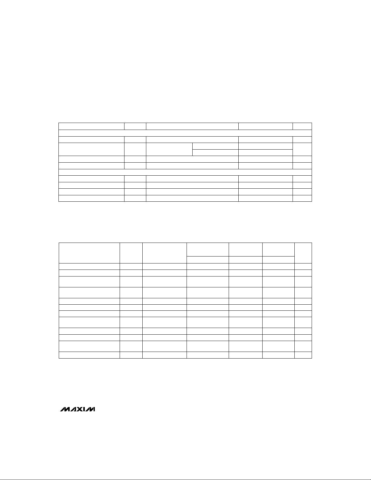
ELECTRICAL CHARACTERISTICS
(VDD= +5V, V
LOGIC OUTPUTS
Output High Voltage
Output Low Voltage
Output Capacitance (Note 4)
POWER SUPPLY
Supply Voltage
Supply Current
Note 1: Total unadjusted error includes offset, full-scale, and linearity errors.
Note 2: Specified with no external load unless otherwise noted.
Note 3: Temperature drift is defined as change in output voltage from +25°C to T
Note 4: Guaranteed by design.
+ = +5V, V
REF
- = GND, Mode 0, TA= T
REF
DB0–DB7, –I—N—T–; I
OH
DB0–DB7, –I—N—T–; RDY
V
OL
DB0–DB7, RDY; V
OUT
5V ±5% for specified performance
DD
–C—S–= –R—D–
DD
VDD= ±5%
MIN
= 2.4V
to T
, unless otherwise noted.)
MAX
CONDITIONS
= -360µA
OUT
I
= 1.6mA
OUT
I
= 2.6mA
OUT
= 0V to V
OUT
DD
MIN
or T
MAX
divided by (25 - T
MIN
TIMING CHARACTERISTICS (Note 5)
(VDD= +5V, V
–C—S–
to –R—D–Setup Time
–C—S–
to –R—D–Hold Time
Multiplexer Address
Setup Time
Multiplexer Address
Hold Time
–C—S–
to RDY Delay
Conversion Time (Mode 0)
Data Access Time After –R—D
Data Access Time
After –I—N—T–, Mode 0
–R—D–
to –I—N—T–Delay (Mode 1)
Data Hold Time
Delay Time
Between Conversions
–R—D–
Pulse Width (Mode 1)
Note 5: All input control signals are specified with t
Note 6: Measured with load circuits of Figure 1 and defined as the time required for an output to cross 0.8V or 2.4V.
Note 7: Defined as the time required for the data lines to change 0.5V when loaded with the circuits of Figure 2.
+ = +5V, V
REF
- = GND, Mode 0, TA= T
REF
SYMBOLPARAMETER
t
CSS
t
CSH
t
AS
t
AH
t
t
–
t
ACC1
t
ACC2
t
CL= 50pF, RL= 5kΩ
RDY
CRD
(Note 6)
(Note 6)
CL= 50pF
INTH
(Note 7)
t
DH
t
P
t
RD
to T
MIN
CONDITIONS
, unless otherwise noted.)
MAX
TA= +25°C
MAX15_ _C/E
MX782_K/L/B/C
MAX15_ _M
MX782_T/U
MIN MAX MIN MAXMIN TYP MAX
0
0
0
30
30 40
1.6 2.0
20 50
40 75
500
60 600
= tF= 20ns (10% to 90% of +5V) and timed from a 1.6V voltage level.
R
0
0
0
35
60
2.4
85
110
60
100
60
70
500
80 500 80 400
0
0
0
40
600
0.4
0.4
) or (T
60
2.8
120
70
100
70
MAX
MX7824/MX7828
UNITSMIN TYP MAXSYMBOLPARAMETER
V4.0V
V
µA±3Three-State Output Current
pF58C
V4.75 5.25V
mA15I
mW25 75Power Dissipation
LSB±1/16 ±1/4PSSPower-Supply Sensitivity
- 25).
UNITS
ns
ns
ns
ns
ns
µs
ns
ns
ns
ns
ns
ns
_______________________________________________________________________________________ 3

CMOS, High-Speed, 8-Bit ADCs
with Multiplexer
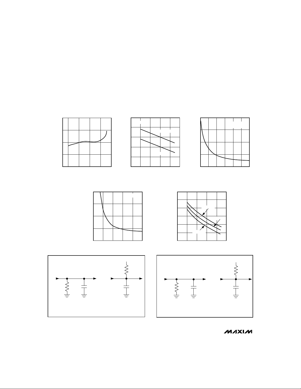
__________________________________________Typical Operating Characteristics
(TA = +25°C, unless otherwise noted.)
REFERENCE TEMPERATURE
DRIFT (MAX154/MAX158 ONLY)
2.520
2.510
2.500
REF OUT VOLTAGE (V)
2.490
MX7824/MX7828
2.480
-50 150
050
AMBIENT TEMPERATURE (°C)
LINEARITY ERROR (LSB)
100
ACCURACY vs. V
(V
2.0
1.5
1.0
0.5
0
REF
05
OUTPUT CURRENT
20
MX7824/28-1
16
12
8
OUTPUT CURRENT (mA)
4
0
= V
REF
+ - V
REF
REF
3412
V
(V)
REF
vs. TEMPERATURE
VDD = 5V
I
I
SINK VOUT
-100 150
-50 0 50
AMBIENT TEMPERATURE (°C)
-)
V
= 5V
DD
MX7824/28-4
SOURCE VOUT
= 0.4V
ACCURACY vs. DELAY BETWEEN
2.0
MX7824/28-2
= 2.4V
100
POWER-SUPPLY CURRENT vs. TEMPERATURE
(NOT INCLUDING REFERENCE LADDER)
8
7
6
5
4
– SUPPLY CURRENT (mA)
DD
I
3
2
-100 150
1.5
1.0
LINEARITY ERROR (LSB)
0.5
0
V
= 4.75V
DD
AMBIENT TEMPERATURE (°C)
CONVERSIONS (tp)
300 900
V
= 5.25V
DD
V
50 100-50 0
V
= 5V
DD
V
REF
700 800400 500 600
tp (ns)
MX7824/28-5
= 5V
DD
= 5V
MX7824/28-3
+5V
3k
DBN
3k
100pF
DGND
a. High-Z to V
Figure 1. Load Circuits for Data-Access Time Test
OH
DBN
100pF
b. High-Z to V
DGND
DBN
3k
10pF
DBN
DGND
OL
a. V
High-Z b. V
OH to
Figure 2. Load Circuits for Data-Hold Time Test
4 _______________________________________________________________________________________
+5V
OL to
3k
10pF
DGND
High-Z
 Loading...