For free samples & the latest literature: http://www.maxim-ic.com, or phone 1-800-998-8800
_______________General Description
Maxim’s MX7575/MX7576 are high-speed (5µs/10µs),
microprocessor (µP) compatible, 8-bit analog-to-digital
converters (ADCs). The MX7575 provides an on-chip
track/hold function that allows full-scale signals up to
50kHz (386mV/µs slew rate) to be acquired and digitized accurately. Both ADCs use a successive-approximation technique to achieve their fast conversions and
low power dissipation. The MX7575/MX7576 operate
with a +5V supply and a 1.23V external reference. They
accept input voltages ranging from 0V to 2V
REF
.
The MX7575/MX7576 are easily interfaced to all popular 8-bit µPs through standard CS and RD control signals. These signals control conversion start and data
access. A BUSY signal indicates the beginning and
end of a conversion. Since all the data outputs are
latched and three-state buffered, the MX7575/MX7576
can be directly tied to a µP data bus or system l/O port.
Maxim also makes the MAX165, a plug-in replacement
for the MX7575 with an internal 1.23V reference. For
applications that require a differential analog input and
an internal reference, the MAX166 is recommended.
________________________Applications
Digital Signal Processing
High-Speed Data Acquisition
Telecommunications
Audio Systems
High-Speed Servo Loops
Low-Power Data Loggers
____________________________Features
♦ Fast Conversion Time: 5µs (MX7575)
10µs (MX7576)
♦ Built-In Track/Hold Function (MX7575)
♦ Low Total Unadjusted Error (±1LSB max)
♦ 50kHz Full-Power Signal Bandwidth (MX7575)
♦ Single +5V Supply Operation
♦ 8-Bit µP Interface
♦ 100ns Data-Access Time
♦ Low Power: 15mW
♦ Small-Footprint Packages
MX7575/MX7576
CMOS, µP-Compatible, 5µs/10µs, 8-Bit ADCs
________________________________________________________________
Maxim Integrated Products
1
DAC
COMP
LATCH AND
THREE-STATE
OUTPUT DRIVERS
SAR
TRACK/
HOLD
CLOCK
OSCILLATOR
CONTROL
LOGIC
AIN
AGND
REF
CLK
CS
RD
V
DD
BUSY DGND
TP
16
18
49
6
14
D7
.
.
D0
15
17
5
1
2
3
MX7575
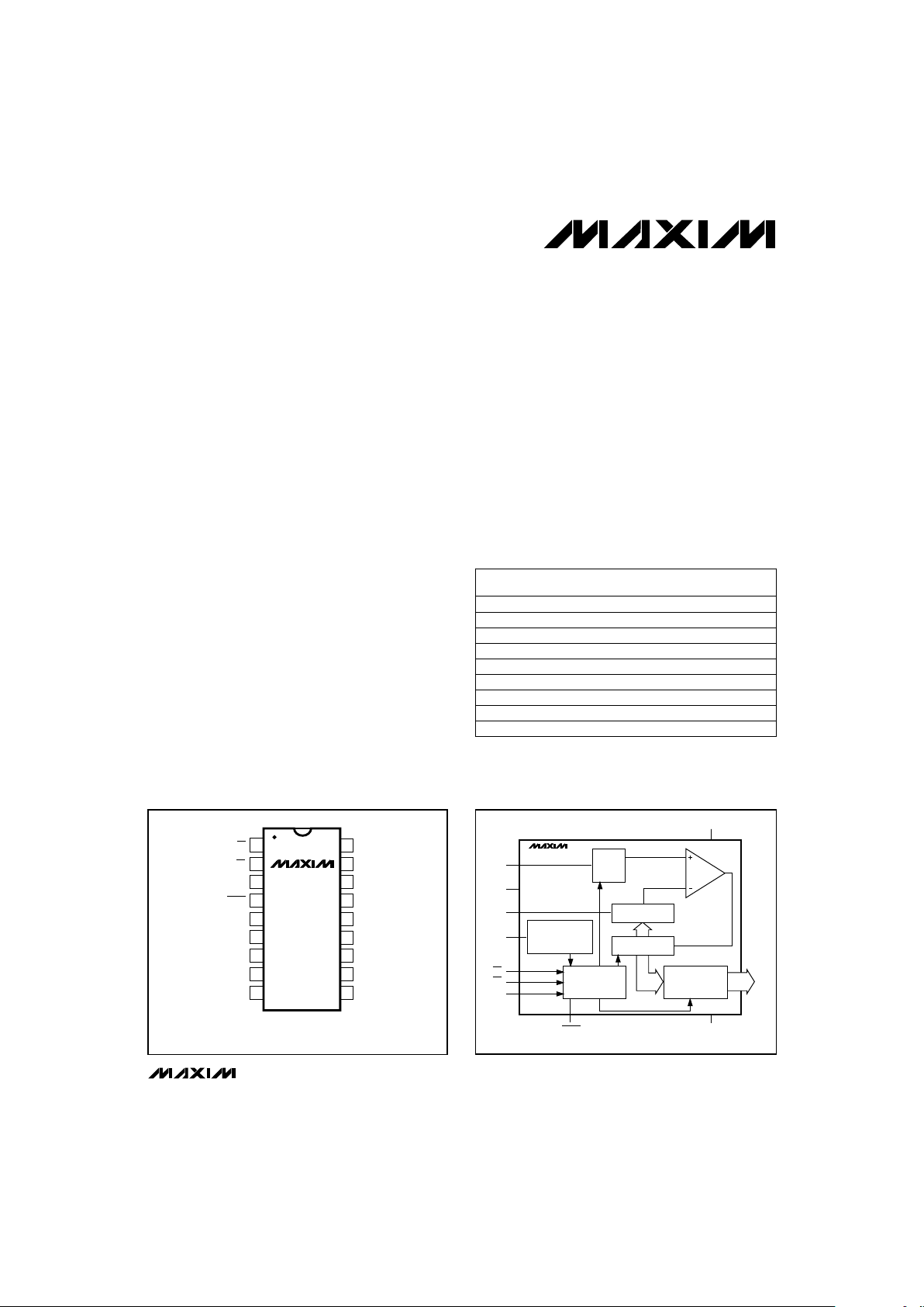
Functional Diagrams continued at end of data sheet.
_______________Functional Diagrams
18
17
16
15
14
13
12
11
1
2
3
4
5
6
7
8
V
DD
REF
AIN
AGND
D0 (LSB)
D1
D2
D3
D4
CS
RD
TP (MODE)
BUSY
CLK
D7 (MSB)
D6
D5
DGND
TOP VIEW
10
9
DIP/SO
MX7575
MX7576
( ) ARE FOR MX7576 ONLY.
Pin Configurations continued at end of data sheet.
_________________Pin Configurations
19-0876; Rev 1; 5/96
PART
MX7575JN
MX7575KN
MX7575JCWN 0°C to +70°C
0°C to +70°C
0°C to +70°C
TEMP. RANGE PIN-PACKAGE
18 Plastic DIP
18 Plastic DIP
18 Wide SO
______________Ordering Information
Ordering Information continued at end of data sheet.
* Contact factory for dice specifications.
** Contact factory for availability.
MX7575KCWN 0°C to +70°C 18 Wide SO
MX7575JP 0°C to +70°C 20 PLCC
MX7575KP 0°C to +70°C 20 PLCC
INL
(LSB)
±1
±1/2
±1
±1/2
±1
±1/2
MX7575J/D 0°C to +70°C Dice* ±1
MX7575AQ -25°C to +85°C 18 CERDIP**
MX7575BQ -25°C to +85°C 18 CERDIP**±1±1/2

MX7575/MX7576
CMOS, µP-Compatible, 5µs/10µs, 8-Bit ADCs
2 _______________________________________________________________________________________
ABSOLUTE MAXIMUM RATINGS
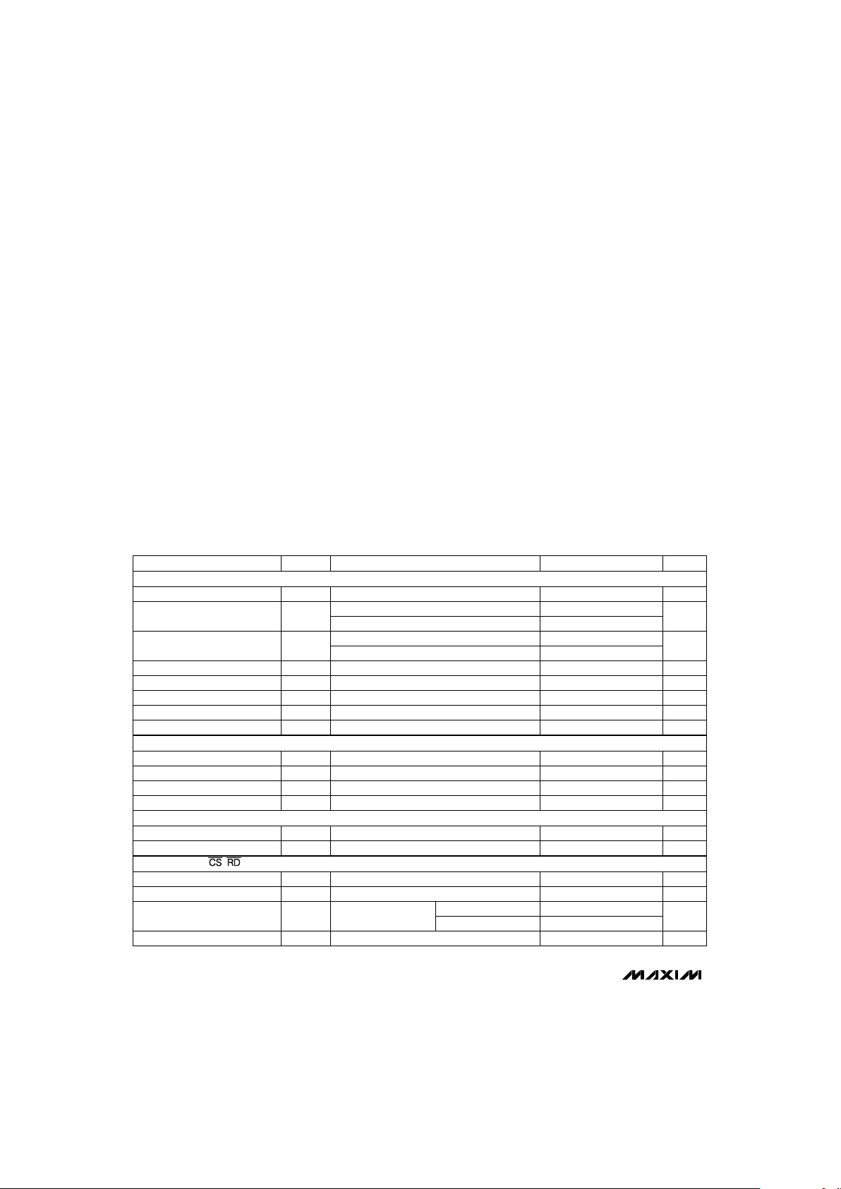
ELECTRICAL CHARACTERISTICS
(VDD= +5V; V
REF
= 1.23V; AGND = DGND = 0V; f
CLK
= 4MHz external for MX7575; f
CLK
= 2MHz external for MX7576;
T
A
= T
MIN
to T
MAX
, unless otherwise noted.)
Stresses beyond those listed under “Absolute Maximum Ratings” may cause permanent damage to the device. These are stress ratings only, and functional
operation of the device at these or any other conditions beyond those indicated in the operational sections of the specifications is not implied. Exposure to
absolute maximum rating conditions for extended periods may affect device reliability.
VDDto AGND...............................................................-0.3V, +7V
V
DD
to DGND ..............................................................-0.3V, +7V
AGND to DGND...............................................-0.3V, V
DD
+ 0.3V
Digital Input Voltage to DGND
(CS, RD, TP, MODE)......................................-0.3V, V
DD
+ 0.3V
Digital Output Voltage to DGND
(BUSY, D0–D7)..............................................-0.3V, V
DD
+ 0.3V
CLK Input Voltage to DGND............................-0.3V, V
DD
+ 0.3V
REF to AGND...................................................-0.3V, V
DD
+ 0.3V
AIN to AGND....................................................-0.3V, V
DD
+ 0.3V
Continuous Power Dissipation (T
A
= +70°C)
Plastic DIP (derate 11.11mW/°C above +70°C)...............889mW
Wide SO (derate 9.52mW/°C above +70°C)..................762mW
CERDIP (derate 10.53mW/°C above +70°C).................842mW
PLCC (derate 10.00mW/°C above +70°C) ....................800mW
Operating Temperature Ranges
MX757_J/K............................................................0°C to +70°C
MX757_A/B........................................................-25°C to +85°C
MX757_JE/KE ....................................................-40°C to +85°C
MX757_S/T.......................................................-55°C to +125°C
Storage Temperature Range.............................-65°C to +160°C
Lead Temperature (soldering,10sec)..............................+300°C
V
IN
= 0V or V
DD
±10
I
IN
Input Current µA
±1
V2.4V
INH
Input High Voltage
V0.8V
INL
Input Low Voltage
µA500I
REF
Reference Current
V1.23V
REF
Reference Voltage
dB45SNRSignal-to-Noise Ratio (Note 2)
V/µs0.386Slew Rate, Tracking
MΩ10DC Input Impedance
V02V
REF
Voltage Range
±1
Bits8Resolution
ppm/°C±5Offset Tempco
LSB±1/2Offset Error (Note 1)
ppm/°C±5Full-Scale Tempco
LSB±1Full-Scale Error
LSB
±2
TUETotal Unadjusted Error
±1/2
LSB
±1
INLRelative Accuracy
Bits8No-Missing-Codes Resolution
UNITSMIN TYP MAXSYMBOLPARAMETER
TA= T
MIN
to T
MAX
TA= +25°C
MX757_K/B/T
±5% variation for specified performance
MX7575, VIN= 2.46V
p-p
at 10kHz, Figure 13
MX7575
MX757_J/A/S
MX757_K/B/T
MX757_J/A/S
1LSB = 2V
REF
/256
CONDITIONS
pF10C
IN
Input Capacitance (Note 2)
ACCURACY
ANALOG INPUT
REFERENCE INPUT
LOGIC INPUTS CS, RD, MODE

MX7575/MX7576
CMOS, µP-Compatible, 5µs/10µs, 8-Bit ADCs
_______________________________________________________________________________________ 3
Note 1: Offset Error is measured with respect to an ideal first-code transition that occurs at 1/2LSB.
Note 2: Sample tested at +25°C to ensure compliance.
Note 3: Accuracy may degrade at conversion times other than those specified.
Note 4: Power-supply current is measured when MX7575/MX7576 are inactive, i.e.:
For MX7575 CS = RD = BUSY = high;
For MX7576 CS = RD = BUSY = MODE = high.
Using recommended
clock components:
R
CLK
= 100kΩ,
C
CLK
= 100pF;
T
A
= +25°C
V
OUT
= 0V to VDD, D0–D7
VIN= 0V
VIN= V
DD
4.75V < VDD< 5.25V LSB±1/4Power-Supply Rejection
mW15Power Dissipation
mA
7
I
DD
Supply Current
36
V5V
DD
Supply Voltage
µs
10 30
Conversion Time with
Internal Clock
515
µs
10
Conversion Time with
External Clock
5
pF10
Floating State Output
Capacitance (Note 2)
µA
±10
Floating State Leakage Current
V2.4V
INH
Input High Voltage
V0.8V
INL
Input Low Voltage
±1
V4.0V
OH
Output High Voltage
V0.4V
OL
Output Low Voltage
700
I
INL
µA
800
Input Low Current
700
I
INH
µA
800
Input High Current
UNITSMIN TYP MAXSYMBOLPARAMETER
MX757_S/T
MX757_J/A/K/B
±5% for specified performance
MX7576
MX7575
MX7576: f
CLK
= 2MHz
TA= +25°C
I
SOURCE
= 40µA
MX7575: f
CLK
= 4MHz
I
SINK
= 1.6mA
MX757_J/A/K/B
MX757_S/T
MX757_J/A/K/B
D0–D7
MX757_S/T
TA= T
MIN
to T
MAX
CONDITIONS
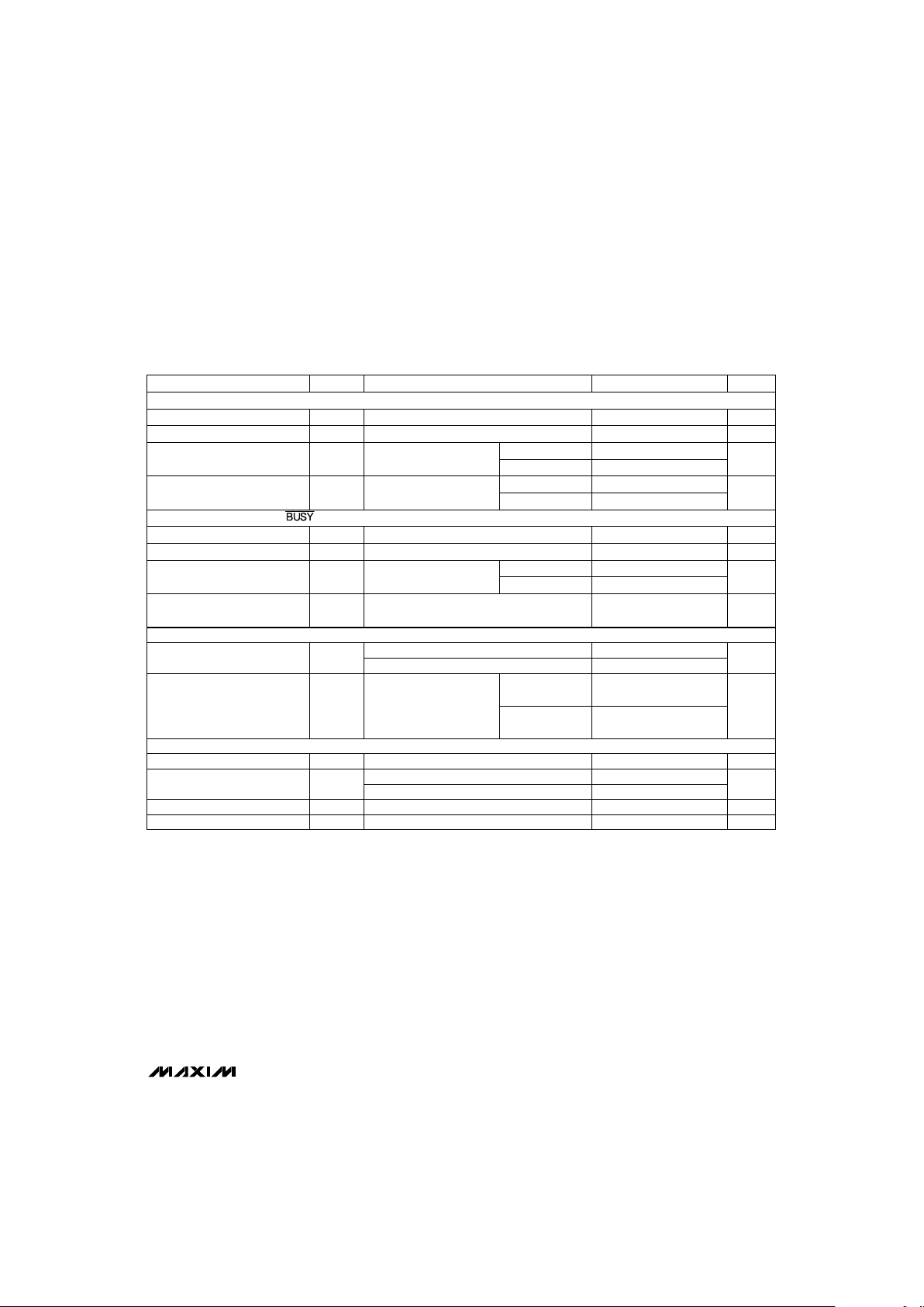
ELECTRICAL CHARACTERISTICS (continued)
(VDD= +5V; V
REF
= 1.23V; AGND = DGND = 0V; f
CLK
= 4MHz external for MX7575; f
CLK
= 2MHz external for MX7576;
T
A
= T
MIN
to T
MAX
, unless otherwise noted.)
CLOCK
LOGIC OUTPUTS (D0–D7,
BUSY
)
CONVERSION TIME (Note 3)
POWER REQUIREMENTS (Note 4)

MX7575/MX7576
CMOS, µP-Compatible, 5µs/10µs, 8-Bit ADCs
4 _______________________________________________________________________________________
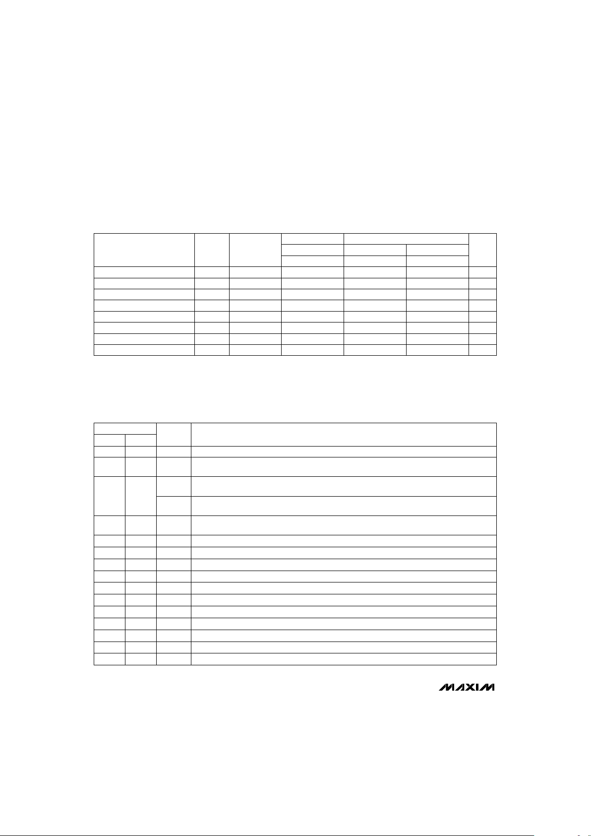
______________________________________________________________Pin Description
DIP/SO
NAME FUNCTION
1
CS Chip Select Input. CS must be low for the device to be selected or to recognize the RD input.
PIN
2
RD
Read Input. RD must be low to access data. RD is also used to start conversions. See the
Microprocessor Interface
section.
TP
(MX7575)
Test Point. Connect to VDD.
7, 8 D6, D5 Three-State Data Outputs, bits 6 and 5
6 D7 Three-State Data Output, bit 7 (MSB)
5 CLK External Clock Input/Internal Oscillator Pin for frequency setting RC components.
4
BUSY
BUSY Output. BUSY going low indicates the start of a conversion. BUSY going high indicates the
end of a conversion.
9 DGND Digital Ground
TA= +25°C TA= T
MIN
to T
MAX
ALL J/K/A/B S/T
PARAMETER SYMBOL CONDITIONS
MIN MAX MIN MAX MIN MAX
UNITS
CS to RD Setup Time
t
1
0 0 0 ns
RD to BUSY Propagation Time
t
2
100 100 120 ns
Data-Access Time after RD
t
3
(Note 6) 100 100 120 ns
RD Pulse Width
t
4
100 100 120 ns
CS to RD Hold Time
t
5
0 0 0 ns
Data-Access Time after BUSY
t
6
(Note 6) 80 80 100 ns
Data-Hold Time t
7
(Note 7) 10 80 10 80 10 100 ns
BUSY to CS Delay
t
8
0 0 0 ns
TIMING CHARACTERISTICS (Note 5)
(VDD= +5V, V
REF
= 1.23V, AGND = DGND = 0V.)
Note 5: Timing specifications are sample tested at +25°C to ensure compliance. All input control signals are specified with
t
r
= tf= 20ns (10% to 90% of +5V) and timed from a voltage level of 1.6V.
Note 6: t3and t6are measured with the load circuits of Figure 1 and defined as the time required for an output to cross 0.8V or 2.4V.
Note 7: t
7
is defined as the time required for the data lines to change 0.5V when loaded with the circuits of Figure 2.
PLCC
2
3
4
8, 9
7
6
5
10
3
MODE
(MX7576)
Mode Input. MODE = low puts the ADC into its asynchronous conversion mode. MODE has to be
tied high for the synchronous conversion mode and the ROM interface mode.
14 D0 Three-State Data Output, bit 0 (LSB)
10–13 D4–D1 Three-State Data Outputs, bits 4–1
15 AGND Analog Ground
16
12–15
17
18 V
DD
Power-Supply Voltage. +5V nominal.
17 REF Reference Input. +1.23V nominal.
— N.C. No Connect
20
19
1, 11
16 AIN Analog Input. 0V to 2V
REF
input range.18
 Loading...