

Page 1
19-0876; Rev 1; 5/96
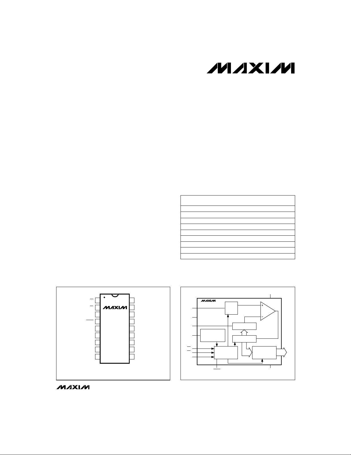
CMOS, µP-Compatible, 5µs/10µs, 8-Bit ADCs
_______________General Description
Maxim’s MX7575/MX7576 are high-speed (5µs/10µs),
microprocessor (µP) compatible, 8-bit analog-to-digital
converters (ADCs). The MX7575 provides an on-chip
track/hold function that allows full-scale signals up to
50kHz (386mV/µs slew rate) to be acquired and digitized accurately. Both ADCs use a successive-approximation technique to achieve their fast conversions and
low power dissipation. The MX7575/MX7576 operate
with a +5V supply and a 1.23V external reference. They
accept input voltages ranging from 0V to 2V
REF
.
The MX7575/MX7576 are easily interfaced to all popular 8-bit µPs through standard CS and RD control signals. These signals control conversion start and data
access. A BUSY signal indicates the beginning and
end of a conversion. Since all the data outputs are
latched and three-state buffered, the MX7575/MX7576
can be directly tied to a µP data bus or system l/O port.
Maxim also makes the MAX165, a plug-in replacement
for the MX7575 with an internal 1.23V reference. For
applications that require a differential analog input and
an internal reference, the MAX166 is recommended.
________________________Applications
Digital Signal Processing
High-Speed Data Acquisition
Telecommunications
Audio Systems
High-Speed Servo Loops
Low-Power Data Loggers
_________________Pin Configurations
____________________________Features
♦ Fast Conversion Time: 5µs (MX7575)
10µs (MX7576)
♦ Built-In Track/Hold Function (MX7575)
♦ Low Total Unadjusted Error (±1LSB max)
♦ 50kHz Full-Power Signal Bandwidth (MX7575)
♦ Single +5V Supply Operation
♦ 8-Bit µP Interface
♦ 100ns Data-Access Time
♦ Low Power: 15mW
♦ Small-Footprint Packages
______________Ordering Information
PART
MX7575JN
MX7575KN
MX7575JCWN 0°C to +70°C
MX7575KCWN 0°C to +70°C 18 Wide SO
MX7575JP 0°C to +70°C 20 PLCC
MX7575KP 0°C to +70°C 20 PLCC
MX7575J/D 0°C to +70°C Dice* ±1
MX7575AQ -25°C to +85°C 18 CERDIP**
MX7575BQ -25°C to +85°C 18 CERDIP**±1±1/2
TEMP. RANGE PIN-PACKAGE
0°C to +70°C
0°C to +70°C
18 Plastic DIP
18 Plastic DIP
18 Wide SO
Ordering Information continued at end of data sheet.
* Contact factory for dice specifications.
** Contact factory for availability.
INL
(LSB)
±1
±1/2
±1
±1/2
±1
±1/2
_______________Functional Diagrams
MX7575/MX7576
V
TOP VIEW
1
CS
2
RD
TP (MODE)
BUSY
CLK
D7 (MSB)
D6
D5
DGND
( ) ARE FOR MX7576 ONLY.
Pin Configurations continued at end of data sheet.
MX7575
3
MX7576
4
5
6
7
8
9
DIP/SO
________________________________________________________________
18
17
16
15
14
13
12
11
10
V
DD
REF
AIN
AGND
D0 (LSB)
D1
D2
D3
D4
MX7575
16
AIN
15
AGND
17
REF
CLOCK
5
CLK
Functional Diagrams continued at end of data sheet.
OSCILLATOR
1
CS
2
RD
3
TP
TRACK/
HOLD
CONTROL
LOGIC
49
BUSY DGND
Maxim Integrated Products
DAC
SAR
DD
18
COMP
LATCH AND
THREE-STATE
OUTPUT DRIVERS
6
D7
.
.
D0
14
1
For free samples & the latest literature: http://www.maxim-ic.com, or phone 1-800-998-8800
Page 2
CMOS, µP-Compatible, 5µs/10µs, 8-Bit ADCs
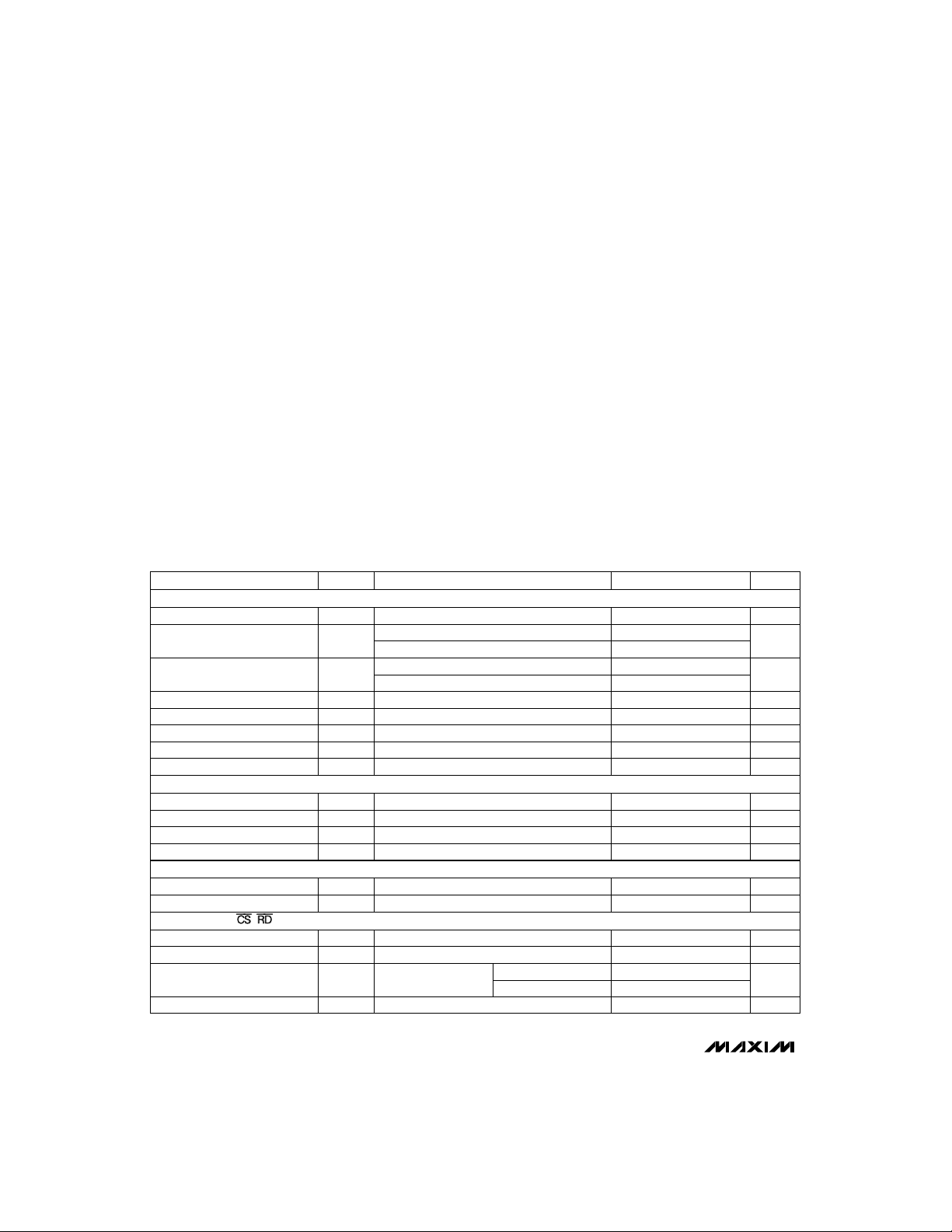
ABSOLUTE MAXIMUM RATINGS
VDDto AGND...............................................................-0.3V, +7V
to DGND ..............................................................-0.3V, +7V
V
DD
AGND to DGND...............................................-0.3V, V
Digital Input Voltage to DGND
(CS, RD, TP, MODE)......................................-0.3V, V
Digital Output Voltage to DGND
(BUSY, D0–D7)..............................................-0.3V, V
CLK Input Voltage to DGND............................-0.3V, V
REF to AGND...................................................-0.3V, V
AIN to AGND....................................................-0.3V, V
Stresses beyond those listed under “Absolute Maximum Ratings” may cause permanent damage to the device. These are stress ratings only, and functional
operation of the device at these or any other conditions beyond those indicated in the operational sections of the specifications is not implied. Exposure to
absolute maximum rating conditions for extended periods may affect device reliability.
DD
DD
DD
DD
DD
DD
+ 0.3V
+ 0.3V
+ 0.3V
+ 0.3V
+ 0.3V
+ 0.3V
Continuous Power Dissipation (T
Plastic DIP (derate 11.11mW/°C above +70°C)...............889mW
= +70°C)
A
Wide SO (derate 9.52mW/°C above +70°C)..................762mW
CERDIP (derate 10.53mW/°C above +70°C).................842mW
PLCC (derate 10.00mW/°C above +70°C) ....................800mW
Operating Temperature Ranges
MX757_J/K............................................................0°C to +70°C
MX757_A/B........................................................-25°C to +85°C
MX757_JE/KE ....................................................-40°C to +85°C
MX757_S/T.......................................................-55°C to +125°C
Storage Temperature Range.............................-65°C to +160°C
Lead Temperature (soldering,10sec)..............................+300°C
MX7575/MX7576
ELECTRICAL CHARACTERISTICS
(VDD= +5V; V
= T
T
to T
A
MIN
ACCURACY
ANALOG INPUT
Voltage Range
REFERENCE INPUT
Reference Voltage
Reference Current
LOGIC INPUTS CS, RD, MODE
Input Low Voltage
Input High Voltage
Input Current µA
Input Capacitance (Note 2)
= 1.23V; AGND = DGND = 0V; f
REF
, unless otherwise noted.)
MAX
TUETotal Unadjusted Error
INLRelative Accuracy
REF
REF
INL
INH
I
IN
IN
= 4MHz external for MX7575; f
CLK
CONDITIONS
MX757_K/B/T
MX757_J/A/S
MX757_K/B/T
MX757_J/A/S
1LSB = 2V
REF
/256
MX7575
MX7575, VIN= 2.46V
at 10kHz, Figure 13
p-p
±5% variation for specified performance
V
IN
= 0V or V
DD
TA= +25°C
TA= T
MIN
to T
MAX
= 2MHz external for MX7576;
CLK
±1
±2
±1/2
±1
REF
±1
±10
UNITSMIN TYP MAXSYMBOLPARAMETER
ppm/°C±5Full-Scale Tempco
ppm/°C±5Offset Tempco
Bits8Resolution
LSB
LSB
Bits8No-Missing-Codes Resolution
LSB±1Full-Scale Error
LSB±1/2Offset Error (Note 1)
V02V
MΩ10DC Input Impedance
V/µs0.386Slew Rate, Tracking
dB45SNRSignal-to-Noise Ratio (Note 2)
V1.23V
µA500I
V0.8V
V2.4V
pF10C
2 _______________________________________________________________________________________
Page 3
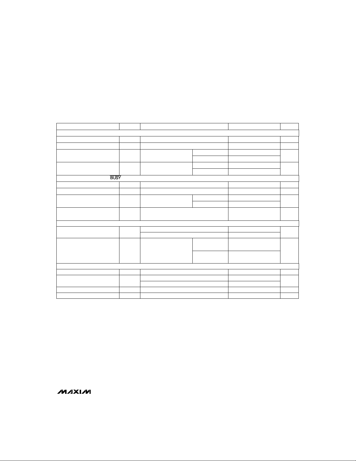
CMOS, µP-Compatible, 5µs/10µs, 8-Bit ADCs
BUSY
ELECTRICAL CHARACTERISTICS (continued)
(VDD= +5V; V
= T
T
to T
A
MIN
CLOCK
Input Low Voltage
Input High Voltage
Input Low Current
Input High Current
LOGIC OUTPUTS (D0–D7,
Output Low Voltage
Output High Voltage
Floating State Leakage Current
Floating State Output
Capacitance (Note 2)
CONVERSION TIME (Note 3)
Conversion Time with
External Clock
Conversion Time with
Internal Clock
POWER REQUIREMENTS (Note 4)
Supply Voltage
Supply Current
Note 1: Offset Error is measured with respect to an ideal first-code transition that occurs at 1/2LSB.
Note 2: Sample tested at +25°C to ensure compliance.
Note 3: Accuracy may degrade at conversion times other than those specified.
Note 4: Power-supply current is measured when MX7575/MX7576 are inactive, i.e.:
For MX7575 CS = RD = BUSY = high;
For MX7576 CS = RD = BUSY = MODE = high.
= 1.23V; AGND = DGND = 0V; f
REF
, unless otherwise noted.)
MAX
INL
INH
I
INL
I
INH
)
OL
OH
DD
I
DD
= 4MHz external for MX7575; f
CLK
CONDITIONS
VIN= 0V
VIN= V
DD
I
= 1.6mA
SINK
I
= 40µA
SOURCE
V
= 0V to VDD, D0–D7
OUT
MX757_J/A/K/B
MX757_S/T
MX757_J/A/K/B
MX757_S/T
TA= +25°C
TA= T
D0–D7
MX7575: f
MX7576: f
CLK
CLK
= 4MHz
= 2MHz
Using recommended
clock components:
= 100kΩ,
R
CLK
= 100pF;
C
CLK
= +25°C
T
A
±5% for specified performance
MX757_J/A/K/B
MX757_S/T
4.75V < VDD< 5.25V LSB±1/4Power-Supply Rejection
MIN
MX7575
MX7576
to T
CLK
MAX
= 2MHz external for MX7576;
UNITSMIN TYP MAXSYMBOLPARAMETER
V0.8V
V2.4V
700
800
700
800
µA
µA
V0.4V
V4.0V
±1
±10
µA
pF10
5
10
µs
515
µs
10 30
V5V
36
mA
7
mW15Power Dissipation
MX7575/MX7576
_______________________________________________________________________________________ 3
Page 4
CMOS, µP-Compatible, 5µs/10µs, 8-Bit ADCs
TIMING CHARACTERISTICS (Note 5)
(VDD= +5V, V
CS to RD Setup Time
RD to BUSY Propagation Time
Data-Access Time after RD
RD Pulse Width
CS to RD Hold Time
Data-Access Time after BUSY
Data-Hold Time t
MX7575/MX7576
BUSY to CS Delay
Note 5: Timing specifications are sample tested at +25°C to ensure compliance. All input control signals are specified with
Note 6: t3and t6are measured with the load circuits of Figure 1 and defined as the time required for an output to cross 0.8V or 2.4V.
Note 7: t
______________________________________________________________Pin Description
= 1.23V, AGND = DGND = 0V.)
REF
TA= +25°C TA= T
PARAMETER SYMBOL CONDITIONS
t
1
t
2
t
(Note 6) 100 100 120 ns
3
t
4
t
5
t
(Note 6) 80 80 100 ns
6
(Note 7) 10 80 10 80 10 100 ns
7
t
8
t
= tf= 20ns (10% to 90% of +5V) and timed from a voltage level of 1.6V.
r
is defined as the time required for the data lines to change 0.5V when loaded with the circuits of Figure 2.
7
ALL J/K/A/B S/T
MIN MAX MIN MAX MIN MAX
0 0 0 ns
100 100 120 ns
100 100 120 ns
0 0 0 ns
0 0 0 ns
MIN
to T
MAX
UNITS
PIN
DIP/SO
10–13 D4–D1 Three-State Data Outputs, bits 4–1
4 _______________________________________________________________________________________
PLCC
1
2
3
4
5 CLK External Clock Input/Internal Oscillator Pin for frequency setting RC components.
6 D7 Three-State Data Output, bit 7 (MSB)
7, 8 D6, D5 Three-State Data Outputs, bits 6 and 5
9 DGND Digital Ground
12–15
14 D0 Three-State Data Output, bit 0 (LSB)
15 AGND Analog Ground
16 AIN Analog Input. 0V to 2V
17 REF Reference Input. +1.23V nominal.
18 V
— N.C. No Connect
1, 11
NAME FUNCTION
2
3
4
5
6
7
8, 9
10
16
17
19
20
CS Chip Select Input. CS must be low for the device to be selected or to recognize the RD input.
Read Input. RD must be low to access data. RD is also used to start conversions. See the
RD
TP
(MX7575)
MODE
(MX7576)
BUSY
DD
Microprocessor Interface
Test Point. Connect to VDD.
Mode Input. MODE = low puts the ADC into its asynchronous conversion mode. MODE has to be
tied high for the synchronous conversion mode and the ROM interface mode.
BUSY Output. BUSY going low indicates the start of a conversion. BUSY going high indicates the
end of a conversion.
Power-Supply Voltage. +5V nominal.
REF
section.
input range.18
Page 5

CMOS, µP-Compatible, 5µs/10µs, 8-Bit ADCs
+5V
3k
D_ D_
100pF
DGND DGND
a) HIGH-Z TO V
NOTE: D_ REPRESENTS ANY OF THE DATA OUTPUTS
Figure 1. Load Circuits for Data-Access Time Test
OH
b) HIGH-Z TO V
100pF3k
OL
_______________Detailed Description
The MX7575 and MX7576 use the successive-approximation technique to convert an unknown analog input
voltage to an 8-bit digital output code (see
Diagrams
). The MX7575 samples the input voltage on
an internal capacitor once (at the beginning of the conversion), while the MX7576 samples the input signal
eight times during the conversion (see
Track/Hold
and
MX7576 Analog Input
internal DAC is initially set to half scale, and the comparator determines whether the input signal is larger
than or smaller than half scale. If it is larger than half
scale, the DAC MSB is kept. But if it is smaller, the MSB
is dropped. At the end of each comparison phase, the
SAR (successive-approximation register) stores the
results of the previous decision and determines the
next trial bit. This information is then loaded into the
DAC after each decision. As the conversion proceeds,
the analog input is approximated more closely by comparing it to the combination of the previous DAC bits
and a new DAC trial bit. After eight comparison cycles,
the eight bits stored in the SAR are latched into the output latches. At the end of the conversion, the BUSY signal goes high, and the data in the output latches is
ready for microprocessor (µP) access. Furthermore, the
DAC is reset to half scale in preparation for the next
conversion.
The CS and RD logic inputs are used to initiate conversions and to access data from the devices. The MX7575
and MX7576 have two common interface modes: slowmemory interface mode and ROM interface mode. In
addition, the MX7576 has an asynchronous conversion
mode (MODE pin = low) where continuous conversions
Converter Operation
Functional
MX7575
sections). The
Microprocessor Interface
+5V
3k
D_ D_
10pF
DGND DGND
a) VOH TO HIGH-Z b) VOL TO HIGH-Z
NOTE: D_ REPRESENTS ANY OF THE DATA OUTPUTS
Figure 2. Load Circuits for Data-Hold Time Test
10pF3k
are performed. In the slow-memory interface mode, CS
and RD are taken low to start a conversion and they
remain low until the conversion ends, at which time the
conversion result is latched. This mode is designed for
µPs that can be forced into a wait state. In the ROM
interface mode, however, the µP is not forced into a wait
state. A conversion is started by taking CS and RD low,
and data from the previous conversion is read. At the
end of the most recent conversion, the µP executes a
read instruction and starts another conversion.
For the MX7575, TP should be hard-wired to V
DD
ensure proper operation of the device. Spurious signals
may occur on TP, or excessive currents may be drawn
from VDDif TP is left open or tied to a voltage other than
VDD.
Slow-Memory Mode
Figure 3 shows the timing diagram for slow-memory
interface mode. This is used with µPs that have a waitstate capability of at least 10µs (such as the 8085A),
where a read instruction is extended to accommodate
slow-memory devices. A conversion is started by executing a memory read to the device (taking CS and RD
low). The BUSY signal (which is connected to the µP
READY input) then goes low and forces the µP into a
wait state. The MX7575 track/hold, which had been
tracking the analog input signal, holds the signal on the
third falling clock edge after RD goes low (Figure 12).
The MX7576, however, samples the analog input eight
times during a conversion (once before each comparator decision). At the end of the conversion, BUSY
returns high, the output latches and buffers are updated with the new conversion result, and the µP completes the memory read by acquiring this new data.
The fast conversion time of the MX7575/MX7576
ensures that the µP is not forced into a wait state for an
excessive amount of time. Faster versions of many µPs,
MX7575/MX7576
to
_______________________________________________________________________________________ 5
Page 6

CMOS, µP-Compatible, 5µs/10µs, 8-Bit ADCs
BUSY
DATA
CS
RD
HIGH-
IMPEDANCE
BUS
t
1
t
2
t
CONV
t
3
OLD DATA
t
6
NEW
DATA
t
7
t
5
IMPEDANCE
Figure 3. Slow-Memory Interface Timing Diagram
A8–A15
MX7575/MX7576
8085A-2
S0 RD
ALE
AD0–AD7
READY
* SOME CIRCUITRY OMITTED FOR CLARITY
S0 IS LOW FOR READ CYCLES
ADDRESS
LATCH
ADDRESS BUS
ADDRESS
DECODE
DATA BUS
+5V
TP/MODE
CS
MX7576
BUSY
D0–D7
MX7575*
Figure 4. MX7575/MX7576 to 8085A-2 Slow-Memory Interface
including the 8085A-2, test the status of the READY
input immediately after the start of an instruction cycle.
Therefore, if the MX7575/MX7576 are to be effective in
placing the µP in a wait state, their BUSY output should
go low very early in the cycle. When using the 8085A-2,
the earliest possible indication of an upcoming read
operation is provided by the S0 status signal. Thus, S0,
which is low for a read cycle, should be connected to
the RD input of the MX7575/MX7576. Figure 4 shows
the connection diagram for the 8085A-2 to the
MX7575/MX7576 in slow-memory interface mode.
ROM Interface Mode
Figure 5 shows the timing diagram for ROM interface
mode. In this mode, the µP does not need to be placed
in a wait state. A conversion is started with a read
instruction (RD and CS go low), and old data is
accessed. The BUSY signal then goes low to indicate
the start of a conversion. As before, the MX7575
track/hold acquires the signal on the third falling clock
edge after RD goes low, while the MX7576 samples it
eight times during a conversion. At the end of a conversion (BUSY going high), another read instruction always
accesses the new data and normally starts a second
conversion. However, if RD and CS go low within one
HIGH-
BUS
CS
BUSY
DATA
RD
IMPEDANCE
t
1
HIGH-
BUS
t
2
t
3
t
4
OLD
DATA
t
5
t
8
t
7
HIGH-IMPEDANCE BUS
t
3
NEW
DATA
t
7
IMPEDANCE
HIGH-
BUS
Figure 5. ROM Interface Timing Diagram
A0–A15
6502-6809
R/W
Φ2 OR E
D0–D7
* SOME CIRCUITRY OMITTED FOR CLARITY
ADDRESS BUS
ADDRESS
EN
DECODE
DATA BUS
+5V
TP/MODE
CS
RD
D0–D7
MX7575*
MX7576
Figure 6. MX7575/MX7576 to 6502/6809 ROM Interface
external clock period of BUSY going high, then the second conversion is not started. Furthermore, for correct
operation in this mode, RD and CS should not go low
before BUSY returns high.
Figures 6 and 7 show the connection diagrams for
interfacing the MX7575/MX7576 in the ROM interface
mode. Figure 6 shows the connection diagram for the
6502/6809 µPs, and Figure 7 shows the connections for
the Z-80.
Due to their fast interface timing, the MX7575/MX7576
will interface to the TMS32010 running at up to 18MHz.
Figure 8 shows the connection diagram for the
TMS32010. In this example, the MX7575/MX7576 are
mapped as a port address. A conversion is initiated by
using an IN A and a PA instruction, and the conversion
result is placed in the TMS32010 accumulator.
Asynchronous Conversion Mode (MX7576)
Tying the MODE pin low places the MX7576 into a continuous conversion mode. The RD and CS inputs are
only used for reading data from the converter. Figure 9
shows the timing diagram for this mode of operation,
and Figure 10 shows the connection diagram for the
8085A. In this mode, the MX7576 looks like a ROM to
6 _______________________________________________________________________________________
Page 7

CMOS, µP-Compatible, 5µs/10µs, 8-Bit ADCs
Z-80
MREQ
RD
DB7
DB0
* SOME CIRCUITRY OMITTED FOR CLARITY
Figure 7. MX7575/MX7576 to Z-80 ROM Interface
ADDRESS BUS
ADDRESS
EN
DECODE
DATA BUS
+5V
TP/MODE
CS
RD
D7
D0
MX7575*
MX7576
BUSY
DATA
CS
RD
t
1
t
3
HIGH-
IMPEDANCE
BUS
t
4
VALID
DATA
UPDATE
LATCH
t
5
t
7
HIGH-IMPEDANCE BUS
VALID
DATA
DEFER
UPDATING
HIGH-
IMPEDANCE
BUS
Figure 9. MX7576 Asynchronous Conversion Mode Timing
Diagram
MX7575/MX7576
PA2
PA0
TMS32010
MEN
DEN
DB7
DB0
* SOME CIRCUITRY OMITTED FOR CLARITY
ADDRESS BUS
ADDRESS
EN
DECODE
DATA BUS
+5V
TP/MODE
CS
RD
D7
D0
MX7575*
MX7576
Figure 8. MX7575/MX7576 to TMS32010 ROM Interface
the µP, in that data can be accessed independently of
the clock. The output latches are normally updated on
the rising edge of BUSY. But if CS and RD are low
when BUSY goes high, the data latches are not updated until one of these inputs returns high. Additionally,
the MX7576 stops converting and BUSY stays high until
RD or CS goes high. This mode of operation allows a
simple interface to the µP.
Processor Interface for Signal Acquisition (MX7575)
In many applications, it is necessary to sample the
input signal at exactly equal intervals to minimize errors
due to sampling uncertainty or jitter. In order to achieve
this objective with the previously discussed interfaces,
the user must match software delays or count the number of elapsed clock cycles. This becomes difficult in
interrupt-driven systems where the uncertainty in interrupt servicing delays is another complicating factor.
The solution is to use a real-time clock to control the
start of a conversion. This should be synchronous with
ADDRESS
LATCH
ADDRESS BUS
ADDRESS
ENCODE
DATA BUS
MODE
CS
D0–D7
MX7576*
A0–A15
8085A
RD RD
ALE
AD0–AD7
* SOME CIRCUITRY OMITTED FOR CLARITY
Figure 10. MX7576 to 8085A Asynchronous Conversion Mode
Interface
the CLK input to the ADC (both should be derived from
the same source), because the sampling instants occur
three clock cycles after CS and RD go low. Therefore,
the sampling instants occur at exactly equal intervals if
the conversions are started at equal intervals. In this
scheme, the output data is fed into a FIFO latch, which
allows the µP to access data at its own rate. This guarantees that data is not read from the ADC in the middle
of a conversion. If data is read from the ADC during a
conversion, the conversion in progress may be disturbed, but the accessed data that belonged to the previous conversion will be correct.
The track/hold starts holding the input on the third
falling edge of the clock after CS and RD go low. If CS
and RD go low within 20ns of a falling clock edge, the
ADC may or may not consider this falling edge as the
first of the three edges that determine the sampling
instant. Therefore, the CS and RD should not be
allowed to go low within this period when sampling
accuracy is required.
_______________________________________________________________________________________ 7
Page 8

CMOS, µP-Compatible, 5µs/10µs, 8-Bit ADCs
The track/hold consists of a sampling capacitor and a
MX7575 Track/Hold
switch to capture the input signal. The simplified diagram of this block is shown in Figure 11. At the beginning of the conversion, switch S1 is closed, and the
input signal is tracked. The input signal is held (switch
S1 opens) on the third falling edge of clock after CS
and RD go low (Figure 12). This allows a minimum of
two clock cycles for the input capacitor to be charged
to the input voltage through the switch resistance. The
time required for the hold capacitor to settle to ±1/4LSB
is typically 7ns. Therefore, the input signal is allowed
ample time to settle before it is acquired by the
track/hold. When a conversion ends, switch S1 closes,
and the input signal is tracked.
The track/hold is capable of acquiring signals with slew
MX7575/MX7576
rates of up to 386mV/µs (or equivalently a 50kHz sine
wave with 2.46Vp-p amplitude). Figure 13 shows the
signal-to-noise ratio (SNR) versus input frequency for
the ADC. The SNR plot is generated at a sampling rate
of 200kHz using sinusoidal inputs with a peak-to-peak
amplitude of 2.46V. The reconstructed sine wave is
passed through a 50kHz 8th-order Chebychev filter.
The improvement in SNR at high frequencies is due to
the filter cutoff.
The switching nature of the analog input results in transient currents that charge the input capacitance of the
track/hold. Keep the driving source impedance low
(below 2kΩ), so that the settling characteristics of the
track/hold are not degraded. A low driving impedance
also minimizes undesirable noise pickup and reduces
DC errors caused by transient currents at the analog
input. As with any ADC, it is important to keep external
sources of noise to a minimum during a conversion.
Therefore, keep the data bus as quiet as possible during a conversion, especially when the track/hold is
making the transition to the hold mode.
For conversion times that are significantly longer than
5µs, the device’s accuracy may degrade slightly, as
shown in Figure 14. This degradation is due to the
charge that is lost from the hold capacitor in the presence of small on-chip leakage currents.
R
ON
S1
CH
2pF
V
IN
Figure 11. Equivalent Input Circuit
CS
0.5pF
500Ω
The MX7576 analog input can also be modeled with the
MX7576 Analog Input
switch and capacitor as shown in Figure 11. However,
unlike the MX7575, the MX7576 samples the input voltage eight times during a conversion (once before each
comparator decision). Therefore, the precautions that
apply to the MX7575 also apply to the MX7576. These
include minimizing the analog source impedance and
reducing noise coupling from the digital circuitry during
a conversion, especially near a sampling instant.
Reference Input
The high speed of this ADC can be partially attributed to
the “inverted voltage output” topology of the DAC that it
uses. This topology provides low offset and gain errors
and fast settling times. The input current to the DAC,
however, is not constant. During a conversion, as different DAC codes are tried, the DC impedance of the DAC
can vary between 6kΩ and 18kΩ. Furthermore, when
the DAC codes change, small amounts of transient current are drawn from the reference input. These characteristics require a low DC and AC driving impedance for
the reference circuitry to minimize conversion errors.
Figure 15 shows the reference circuitry recommended
to drive the reference input of the MX7575/MX7576.
CS
RD
BUSY
EXTERNAL
CLOCK
a) WITH EXTERNAL CLOCK
CS
RD
BUSY
INTERNAL
CLOCK
b) WITH INTERNAL CLOCK
Figure 12. MX7575 Track/Hold (Slow-Memory Interface)
Timing Diagrams
INPUT SIGNAL HELD HERE
INPUT SIGNAL HELD HERE
8 _______________________________________________________________________________________
Page 9

CMOS, µP-Compatible, 5µs/10µs, 8-Bit ADCs
40
TA = +25°C
42
44
46
48
SNR (dB)
50
52
54
100 1k 100k
INPUT FREQUENCY (Hz)
Figure 13. MX7575 SNR vs. Input Frequency
2.5
A: TA = +125°C
= +85°C
B: T
A
= +25°C
C: T
A
2.0
1.5
1.0
RELATIVE ACCURACY (LSB)
0.5
0
10 100 10000
CONVERSION TIME (µs)
Figure 14. MX7575 Accuracy vs. Conversion Time
+5V
3.3k
ICL8069
Figure 15. External Reference Circuit
+
_
1.23V
+
10k
A B C
1000
0.1µF47µF
MX7575/6 FIG13
MX7575/6 FIG14
REF
The decoupling capacitors are necessary to provide a
low AC source impedance.
Internal/External Clock
The MX7575/MX7576 can be run with either an externally applied clock or their internal clock. In either case,
the signal appearing at the clock pin is internally divided by two to provide an internal clock signal that is relatively insensitive to the input clock duty cycle.
Therefore, a single conversion takes 20 input clock
cycles, which corresponds to 10 internal clock cycles.
Internal Clock
The internal oscillator frequency is set by an external
capacitor, C
, and an external resistor, R
CLK
CLK
, which
are connected as shown in Figure 16a. During a conversion, a sawtooth waveform is generated on the CLK
pin by charging C
CLK
through R
and discharging it
CLK
through an internal switch. At the end of a conversion,
the internal oscillator is shut down by clamping the CLK
pin to VDDthrough an internal switch. The circuit for the
internal oscillator can easily be overdriven with an
external clock source.
The internal oscillator provides a convenient clock
source for the MX7575. Figure 17 shows typical conversion times versus temperature for the recommended
R
and C
CLK
tions, the oscillation frequency for this R
combination. Due to process varia-
CLK
CLK/CCLK
combination may vary by as much as ±50% from the
nominal value shown in Figure 17. Therefore, an external clock should be used in the following situations:
1) Applications that require the conversion time to be
within 50% of the minimum conversion time for the
specified accuracy (5µs MX7575/10µs MX7576).
2) Applications in which time-related software con-
straints cannot accommodate conversion-time differences that may occur from unit to unit or over
temperature for a given device.
External Clock
The CLK input of the MX7575/MX7576 may be driven
directly by a 74HC or 4000B series buffer (e g., 4049),
or by an LS TTL output with a 5.6kΩ pull-up resistor. At
the end of a conversion, the device ignores the clock
input and disables its internal clock signal. Therefore,
the external clock may continue to run between conversions without being disabled. The duty cycle of the
external clock may vary from 30% to 70%. As discussed previously, in order to maintain accuracy, clock
rates significantly lower than the data sheet limits
(4MHz for MX7575 and 2MHz for MX7576) should not
be used.
MX7575/MX7576
_______________________________________________________________________________________ 9
Page 10

CMOS, µP-Compatible, 5µs/10µs, 8-Bit ADCs
+5V
47µF
+5V
3.3k
+
47µF
-
MX7575/MX7576
2.46V(max)
+1.23V
0.1µF
0.1µF
18
V
DD
16
17
15
AIN
REF
AGND
MX7575
MX7576
CLK
BUSY
CS
RD
TP/
MODE
9
+5V
5
4
1
2
3
R
CLK
100k, 2%
C
CLK
100pF, 1%
CONTROL INPUTS
D7–D0
DATA OUT
OUTPUT
CODE
1111 1111
1111 1110
1111 1101
0000 0011
0000 0010
0000 0001
0000 0000
1LSB
3LSBs0
2LSBs
AIN, INPUT VOLTAGE (IN TERMS OF LSBs)
FULL-SCALE
TRANSITION
(FS - 3/2LSB)
FS = 2V
REF
2FS
1LSB = –––
256
FS - 1LSB
Figure 16a. Unipolar Configuration Figure 16b. Nominal Transfer Characteristic for Unipolar
Operation
______________ Typical Applications
Unipolar Operation
Figure 16a shows the analog circuit connections for
unipolar operation, and Figure 16b shows the nominal
accurate enough that calibration will not be necessary. If
calibration is not needed, resistors R1–R7 should have a
0.1% tolerance, with R4 and R5 replaced by one 10kΩ
resistor, and R2 and R3 with one 1kΩ resistor. If calibra-
tion is required, follow the steps in the sections below.
transfer characteristic for unipolar operation. Since the
offset and full-scale errors of the MX7575/MX7576 are
very small, it is not necessary to null these errors in
most cases. If calibration is required, follow the steps in
the sections below.
Offset Adjust
The offset error can be adjusted by using the offset trim
capability of an op amp (when it is used as a voltage follower) to drive the analog input, AIN. The op amp should
have a common-mode input range that includes 0V. Set
its initial input to 4.8mV (1/2LSB), while varying its offset
until the ADC output code flickers between 0000 0000
and 0000 0001.
Full-Scale Adjustment
Make the full-scale adjustment by forcing the analog
input, AIN, to 2.445V (FS - 3/2LSB). Then vary the reference input voltage until the ADC output code flickers
between 1111 1110 and 1111 1111.
Bipolar Operation
Figure 18a shows an example of the circuit connection
for bipolar operation, and Figure 18b shows the nominal
transfer characteristic for bipolar operation. The output
code provided by the MX7575 is offset binary. The analog input range for this circuit is ±2.46V (1LSB =
19.22mV), even though the voltage appearing at AIN is
in the 0V to 2.46V range. In most cases, the MX7575 is
Adjust the offset error by applying an analog input volt-
age of 2.43V (+FS - 3/2LSB). Then adjust resistor R5
until the output code flickers between 1111 1110 and
1111 1111.
Full-Scale Adjust
Null the full-scale error by applying an analog input
voltage of -2.45V (-FS + 1/2LSB). Then adjust resistor
R3 until the output code flickers between 0000 0000
and 0000 0001.
14
13
12
11
10
CONVERSION TIME (µs)
Figure 17. Typical Conversion Times vs. Temperature Using
Internal Clock
MX7576
9
8
7
-55 -25 25 75
0 12510050
AMBIENT TEMPERATURE (°C)
MX7575
R
C
CLK
CLK
= 100kΩ
= 100pF
Offset Adjust
10 ______________________________________________________________________________________
Page 11

CMOS, µP-Compatible, 5µs/10µs, 8-Bit ADCs
+5V
47µF
+5V
TLC271
R5
5k
R4
8.2k
R7
10k
0.1µF
47µF
+
+5V
R6
3.3k
ICL8069
1.2V
REFERENCE
Figure 18a. MX7575 Bipolar Configuration
0.1µF
17
R1
1k
16
R2
820Ω
R3
500Ω
INPUT VOLTAGE
18
V
DD
REF
MX7575
AIN
AGND DGND
15
MX7575/MX7576
+5V
R
CLK
5
CLK
9
C
100pF
2%
D7–D0
DATA OUT
L
Figure 18b. Nominal Transfer Characteristic for Bipolar
Operation
111...111
111...110
100...010
100...001
100...000
011...111
011...110
000...001
000...000
OUTPUT
CODE
-FS
-1/2LSB
2
1/2LSB
FS
2
FS = 2V
1LSB =
-1LSB
REF
2FS
256
AIN
__________Applications Information
Noise
To minimize noise coupling, keep both the input signal
lead to AIN and the signal return lead from AGND as
short as possible. If this is not possible, a shielded
cable or a twisted-pair transmission line is recommended. Additionally, potential differences between the ADC
ground and the signal-source ground should be minimized, since these voltage differences appear as
errors superimposed on the input signal. To minimize
system noise pickup, keep the driving source resistance below 2kΩ.
Proper Layout
For PC board layouts, take care to keep digital lines
well separated from any analog lines. Establish a single-point, analog ground (separate from the digital system ground) near the MX7575/MX7576. This analog
ground point should be connected to the digital system
ground through a single-track connection only. Any
supply or reference bypass capacitors, analog input filter capacitors, or input signal shielding should be
returned to the analog ground point.
__Functional Diagrams (continued)
V
DD
18
16
AIN
AGND
REF
CLK
MODE
MX7576
15
17
CLOCK
5
OSCILLATOR
1
CS
2
RD
3
CONTROL
LOGIC
49
BUSY DGND
DAC
SAR
COMP
LATCH AND
THREE-STATE
OUTPUT DRIVERS
6
D7
.
.
D0
14
______________________________________________________________________________________ 11
Page 12

CMOS, µP-Compatible, 5µs/10µs, 8-Bit ADCs
____Pin Configurations (continued)
TOP VIEW
TP (MODE)
D7 (MSB)
BUSY
CLK
RD
3
2 1
4
5
6
7
D6
8
CS
MX7575
MX7576
N.C.
DD
V
20 19
REF
18
17
16
15
14
MX7575/MX7576
9
10
11
12
13
( ) ARE FOR MX7576 ONLY.
D5
DGND
PLCC
N.C.
D4
D3
AIN
AGND
D0 (LSB)
D1
D2
_Ordering Information (continued)
PART
MX7575JEWN
MX7575KEWN
MX7575JEQP -40°C to +85°C
MX7575KEQP -40°C to +85°C 20 PLCC
MX7575SQ -55°C to +125°C 18 CERDIP**
MX7575TQ -55°C to +125°C 18 CERDIP**
MX7576JN
MX7576KN
MX7576JCWN 0°C to +70°C
MX7576KCWN 0°C to +70°C 18 Wide SO
MX7576JP 0°C to +70°C 20 PLCC
MX7576KP 0°C to +70°C 20 PLCC
MX7576J/D 0°C to +70°C Dice* ±1
MX7576AQ -25°C to +85°C 18 CERDIP**
MX7576BQ -25°C to +85°C 18 CERDIP**±1±1/2
MX7576JEWN
MX7576KEWN
MX7576JEQP -40°C to +85°C
TEMP. RANGE PIN-PACKAGE
-40°C to +85°C
-40°C to +85°C
18 Wide SO
18 Wide SO
20 PLCC
0°C to +70°C 18 Plastic DIP
0°C to +70°C
18 Plastic DIP
18 Wide SO
-40°C to +85°C 18 Wide SO
-40°C to +85°C
18 Wide SO
20 PLCC
MX7576KEQP -40°C to +85°C 20 PLCC
MX7576SQ -55°C to +125°C 18 CERDIP**
MX7576TQ -55°C to +125°C 18 CERDIP**
* Contact factory for dice specifications.
** Contact factory for availability.
__________________________________________________________Chip Topographies
INL
(LSB)
±1
±1/2
±1
±1/2
±1
±1/2
±1
±1/2
±1
±1/2
±1
±1/2
±1
±1/2
±1
±1/2
±1
±1/2
MX7575
D7
D6
D5
DGND
D4
0.081"
(2.057mm)
D3
D2 D1
*The two AGND pads must both be used (bonded together).
TRANSISTOR COUNT: 768
SUBSTRATE CONNECTED TO V
Maxim cannot assume responsibility for use of any circuitry other than circuitry entirely embodied in a Maxim product. No circuit patent licenses are
implied. Maxim reserves the right to change the circuitry and specifications without notice at any time.
12
__________________Maxim Integrated Products, 120 San Gabriel Drive, Sunnyvale, CA 94086 (408) 737-7600
CLK
BUSY
D0 AGND* AGND*
0.130"
(3.302mm)
DD
N.C.
D5
TP
RD
CS
V
DD
REF
AIN
DGND
D4
0.081"
(2.057mm)
D3
*The two AGND pads must both be used (bonded together).
TRANSISTOR COUNT: 768
SUBSTRATE CONNECTED TO VDD
D6
D2 D1
MX7576
D7
(MSB)
D0
(LSB)
0.130"
(3.302mm)
CLK
MODE
BUSY
AGND* AGND*
N.C.
RD
CS
V
DD
REF
AIN
© 1996 Maxim Integrated Products Printed USA is a registered trademark of Maxim Integrated Products.
 Loading...