

General Description
The MX536A and MX636 are true RMS-to-DC converters. They feature low power and are designed to accept
low-level input signals from 0 to 7V
RMS
for the MX536A
and 0 to 200mV
RMS
for the MX636. Both devices accept
complex input waveforms containing AC and DC components. They can be operated from either a single supply or dual supplies. Both devices draw less than 1mA
of quiescent supply current, making them ideal for battery-powered applications.
Input and output offset, positive and negative waveform
symmetry (DC reversal), and full-scale accuracy are
laser trimmed, so that no external trims are required to
achieve full rated accuracy.
________________________Applications
Digital Multimeters
Battery-Powered Instruments
Panel Meters
Process Control
____________________________Features
♦ True RMS-to-DC Conversion
♦ Computes RMS of AC and DC Signals
♦ Wide Response:
2MHz Bandwidth for V
RMS
> 1V (MX536A)
1MHz Bandwidth for V
RMS
> 100mV (MX636)
♦ Auxiliary dB Output: 60dB Range (MX536A)
50dB Range (MX636)
♦ Single- or Dual-Supply Operation
♦ Low Power: 1.2mA typ (MX536A)
800µA typ (MX636)
MX536A/MX636
True RMS-to-DC Converters
________________________________________________________________
Maxim Integrated Products
1
14
13
12
11
10
9
8
1
2
3
4
5
6
7
+V
S
N.C.
N.C.
N.C.
COMMON
R
L
I
OUT
V
IN
N.C.
-V
S
C
AV
dB
BUF OUT
BUF IN
MX536A
MX636
DIP
TOP VIEW
MX536A
MX636B
TO-100
8
9
10
1
2
3
4
5
6
7
BUF IN
BUF OUT
dB
C
AV
-V
S
+V
S
I
OUT
R
L
COMMON
V
IN
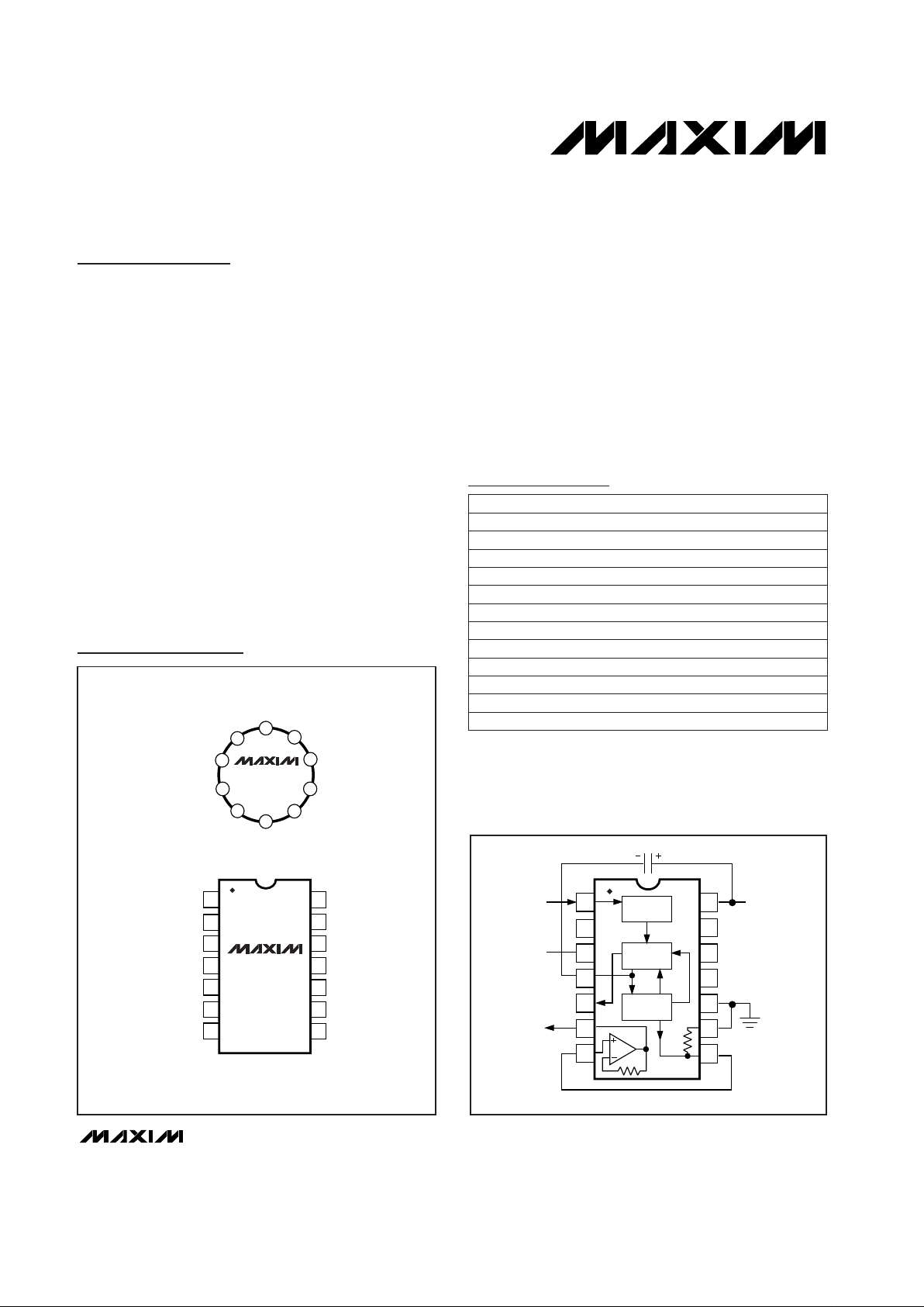
Pin Configurations
14
13
12
11
10
9
8
1
2
3
4
5
6
7
ABSOLUTE
VALUE
SQUARER
DIVIDER
CURRENT
MIRROR
BUF
V
IN
-V
S
+V
S
V
OUT
C
AV
_________Typical Operating Circuits
19-0824; Rev 2; 3/96
PART
MX536AJC/D
MX536AJCWE
MX536AJD 0°C to +70°C
0°C to +70°C
0°C to +70°C
TEMP. RANGE PIN-PACKAGE
Dice**
16 Wide SO
14 Ceramic
Ordering Information
Ordering Information continued at end of data sheet.
*
Maxim reserves the right to ship ceramic packages in lieu of
CERDIP packages.
**
Dice are specified at TA= +25°C.
MX536AJH
MX536AJN 0°C to +70°C
0°C to +70°C 10 TO-100
14 Plastic DIP
MX536AJQ*
MX536AKCWE 0°C to +70°C
0°C to +70°C 14 CERDIP
16 Wide SO
MX536AKD
MX536AKH 0°C to +70°C
0°C to +70°C 14 Ceramic
10 TO-100
MX536AKN 0°C to +70°C 14 Plastic DIP
Pin Configurations continued at end of data sheet.
Typical Operating Circuits continued at end of data sheet.
MX536AKQ* 0°C to +70°C 14 CERDIP
MX536ASD -55°C to +125°C 14 Ceramic
For free samples & the latest literature: http://www.maxim-ic.com, or phone 1-800-998-8800.
For small orders, phone 408-737-7600 ext. 3468.
MX536A/MX636
True RMS-to-DC Converters
2 _______________________________________________________________________________________
ABSOLUTE MAXIMUM RATINGS
ELECTRICAL CHARACTERISTICS—MX536A
(TA= +25°C, +VS= +15V, -VS= -15V, unless otherwise noted.)
Stresses beyond those listed under “Absolute Maximum Ratings” may cause permanent damage to the device. These are stress ratings only, and functional
operation of the device at these or any other conditions beyond those indicated in the operational sections of the specifications is not implied. Exposure to
absolute maximum rating conditions for extended periods may affect device reliability.
Supply Voltage: Dual Supplies (MX536A)............................±18V
(MX636) .............................±12V
Single Supply (MX536A)...........................+36V
(MX636) .............................+24V
Input Voltage (MX536A).......................................................±25V
(MX636).........................................................±12V
Power Dissipation (Package)
Plastic DIP (derate 12mW/°C above +75°C) ...............450mW
Small Outline (derate 10mW/°C above +75°C)............400mW
Ceramic (derate 10mW/°C above +75°C) ...................500mW
TO-100 metal can (derate 7mW/°C above +75°C)......450mW
Output Short-Circuit Duration........................................Indefinite
Operating Temperature Ranges
Commercial (J, K)...............................................0°C to +70°C
Military (S)......................................................-55°C to +125°C
Storage Temperature Range.............................-55°C to +150°C
Lead Temperature (soldering, 10sec)................................300°C
MX536AJ, AS
T
MIN
to +70°C
+70°C to +125°C
MHz2.3
±3dB Bandwidth
450
kHz
90
120
Bandwidth for 1%
Additional Error (0.09dB)
45 kHz
5
-1.0
Additional Error -0.1
% of
Reading
Specified Accuracy
±2 ±0.1
Total Error, External Trim
(Note 1)
mV ±% of
Reading
±3 ±0.3
±2 ±0.2
Total Error, Internal Trim (Note 1)
mV ±% of
Reading
±5 ±0.5
V
OUT
= [avg. (VIN)2] 1/
2
Transfer Equation
±0.1
Total Error vs. DC Reversal
% of
Reading
±0.2
mV ±% of
Reading/V
±0.1 ±0.01Total Error vs. Supply
Total Error vs. Temperature
mV ±% of
Reading/°C
±0.1 ±0.01
±0.05 ±0.005
±0.1 ±0.005
±0.03 ±0.005
UNITS
MIN TYP MAX
PARAMETER
VIN= 1V
VIN= 100mV
VIN= 10mV
MX536AK
VIN= 1V
VIN= 100mV
MX536AJ, AS
VIN= 10mV
Crest Factor = 7
Crest Factor = 3
Crest Factor 1 to 2
MX536AJ
MX536AK
MX536AS
MX536AK
MX536AS
MX536AJ, AS
CONDITIONS
MX536AK
Figure 3 ms/µF C
AV
25Averaging Time Constant
CONVERSION ACCURACY
ERROR vs. CREST FACTOR (Note 2)
FREQUENCY RESPONSE (Note 3)
MX536A/MX636
True RMS-to-DC Converters
_______________________________________________________________________________________ 3
UNITS
MIN TYP MAX
CONDITIONSPARAMETER
V
RMS
0 to 7
±15V Supplies
Continuous RMS Peak Transient
±20 V
PK
0 to 2 V
RMS
Input Signal Range
±5V Supplies
Continuous RMS Peak Transient
±7 V
PK
Safe Input All Supplies ±25 V
PK
Input Resistance 13.33 16.7 20.00 kΩ
MX536AJ, AS 0.8 ±2
mVInput Offset Voltage
MX536AK 0.5 ±1
MX536AJ ±1 ±2
MX536AK ±0.5 ±1TA= +25°C
MX536AS ±2
mV
MX536AJ, AK ±0.1
TA= T
MIN
to T
MAX
MX536AS ±0.2
mV/°C
MX536AJ, AK ±0.1
Offset Voltage
Supply Voltage
MX536AS ±0.2
mV/V
±15V Supplies 0 to 11 12.5
Output Voltage Swing
±5V Supplies 0 to 2
V
Source 5 mA
Output Current
Sink -130 µA
Short Circuit Current 20 mA
Output Resistance 0.5 Ω
MX536AJ ±0.4 ±0.6
dBMX536AK ±0.2 ±0.3Error
VIN= 7mV to 7V
RMS
,
0dB = 1V
RMS
MX536AS ±0.5 ±0.6
Scale Factor -3 mV/dB
Scale Factor TC (Uncompensated) 0.33
% of
Reading/°C
ELECTRICAL CHARACTERISTICS—MX536A (continued)
(TA= +25°C, +VS= +15V, -VS= -15V, unless otherwise noted.)
I
REF
0dB = 1V
RMS
5 20 80 µA
I
REF
Range 1 100 µA
I
OUT
Scale Factor 40 µA/V
RMS
I
OUT
Scale Factor Tolerance ±10 ±20 %
Output Resistance 20 25 30 kΩ
Voltage Compliance
-VSto
(+V
S
- 2.5)
V
INPUT CHARACTERISTICS
OUTPUT CHARACTERISTICS
dB OUTPUT
I
OUT
TERMINAL
MX536A/MX636
True RMS-to-DC Converters
4 _______________________________________________________________________________________
Input Bias Current 20 300 nA
Input Resistance 10
8
Ω
Output Current
Source +5 mA
Sink -130 µA
Short-Circuit Current 20 mA
UNITS
MIN TYP MAX
CONDITIONSPARAMETER
Input and Output Voltage Range
-VSto
(+V
S
- 2.5)
V
Input Offset Voltage RS= 25kΩ
Small-Signal Bandwidth
±0.5 ±4 mV
1 MHz
Slew Rate (Note 4) 5 V/µs
ELECTRICAL CHARACTERISTICS—MX536A (continued)
(TA= +25°C, +VS= +15V, -VS= -15V, unless otherwise noted.)
ELECTRICAL CHARACTERISTICS—MX636
(TA= +25°C, +VS= +3V, -VS= -5V, unless otherwise noted.)
VIN= 200mV
MHz1.5VIN= 200mV
±3dB Bandwidth
900VIN= 100mV
kHz
100VIN= 10mV
130
MX636K
Bandwidth for 1%
Additional Error (0.09dB)
90
VIN= 200mV
kHz
14
VIN= 100mV
MX636J
-0.5
VIN= 10mV
Additional Error -0.2
±% of
Reading
Specified Accuracy
Crest Factor = 6
±0.1 ±0.1
Crest Factor = 3
Total Error, External Trim
(Note 5)
mV ±% of
Reading
±0.3 ±0.1
MX636K
±0.2 ±0.5
MX636J
Total Error, Internal Trim
(Notes 5, 6)
mV ±% of
Reading
±0.5 ±1.0
Crest Factor 1 to 2
V
OUT
= [avg. (VIN)2]
1/2
Transfer Equation
±0.1
Total Error vs. DC Reversal
±% of
Reading
±0.2
mV ±% of
Reading/V
±0.1 ±0.01
MX636J
Total Error vs. Supply
MX636K
Total Error vs. Temperature
(0°C to +70°C)
mV ±% of
Reading/°C
±0.1 ±0.01
±0.1 ±0.005
MX636K
MX636J
UNITSMIN TYP MAXCONDITIONSPARAMETER
BUFFER AMPLIFIER
Figure 3 ms/µF C
AV
25Averaging Time Constant
CONVERSION ACCURACY
ERROR vs. CREST FACTOR (Note 3)
FREQUENCY RESPONSE (Notes 6, 8)

MX536A/MX636
True RMS-to-DC Converters
_______________________________________________________________________________________ 5
ELECTRICAL CHARACTERISTICS—MX636 (continued)
(TA= +25°C, +VS= +3V, -VS= -5V, unless otherwise noted.)
I
REF
±2.8
2 4 8
±2
Input Signal Range
µA
Peak Transient
±5
V
PK
Safe Input
I
REF
Range
±12 V
PK
Input Resistance 5.33 6.7 8.00 kΩ
1 50
MX636J ±0.5
mVInput Offset Voltage
MX636K ±0.2
µA
MX636J ±0.5
TA= +25°C
MX636K ±0.2
mV
I
OUT
Scale Factor
TA= T
MIN
to T
MAX
±10
With Supply Voltage ±0.1
µV/°C
100
Offset Voltage
µA/V
RMS
I
OUT
Scale Factor Tolerance
+3V, -5V Supplies 0 to 1
Output Voltage Swing
±5V to ±16.5V Supplies 0 to 1 1.4
V
-20 ±10 +20 %
Output Resistance 8 10 12 kΩ
UNITSMIN TYP MAXCONDITIONSPARAMETER
MX636J ±0.3 ±0.5
Error 7mV ≤ VIN≤ 300mV
MX636K ±0.1 ±0.2
Scale Factor -3 mV/dB
Scale Factor Tempco
Output Resistance
0 to 200
+0.33 %/°C
8 10 12 kΩ
Voltage Compliance
-VSto
(+V
S
- 2.0)
V
Continuous RMS, All Supplies
All Supplies
±5V Supplies
±2.5V Supplies
+3V, -5V Supplies
mV
RMS
Input and Output Voltage Range
-VSto
(+V
S
- 2)
V
RS= 10kΩ
±0.8 ±2
mVInput Offset Voltage
±0.5 ±1
Input Current 100 300 nA
Input Resistance 10
8
Ω
Source +5 mA
Output Current
Sink -130 µA
Short-Circuit Current 20 mA
Small-Signal Bandwidth 1 MHz
Slew Rate (Note 9) 5 V/µs
0dB = 1V
RMS
MX636J
MX636K
-0.033 dB/°C
mV/V
dB
INPUT CHARACTERISTICS
OUTPUT CHARACTERISTICS (Note 5)
dB OUTPUT
I
OUT
TERMINAL
BUFFER AMPLIFIER

MX536A/MX636
_______________Detailed Description
The MX536A/MX636 uses an implicit method of RMS
computation that overcomes the dynamic range as well
as other limitations inherent in a straightforward computation of the RMS. The actual computation performed
by the MX536A/MX636 follows the equation:
V
RMS
= Avg. [V
IN
2
/V
RMS
]
The input voltage, V
IN
, applied to the MX536A/MX636 is
processed by an absolute-value/voltage to current converter that produces a unipolar current I1(Figure 1).
This current drives one input of a squarer/divider that
produces a current I4that has a transfer function:
I
4
=
I
1
2
I
3
The current I4drives the internal current mirror through
a lowpass filter formed by R1 and an external capacitor, CAV. As long as the time constant of this filter is
greater than the longest period of the input signal, I4is
averaged. The current mirror returns a current, I3, to the
square/divider to complete the circuit. The current I4is
then a function of the average of (I
1
2
/I4), which is equal
to I
1
RMS
.
The current mirror also produces a 2 · I
4
output current,
I
OUT
, that can be used directly or converted to a voltage using resistor R2 and the internal buffer to provide
a low-impedance voltage output. The transfer function
for the MX536A/MX636 is:
V
OUT
= 2 · R2 · I
RMS
= V
IN
The dB output is obtained by the voltage at the emitter
of Q3, which is proportional to the -log VIN. The emitter
follower Q5 buffers and level shifts this voltage so that
the dB output is zero when the externally set emitter
current for Q5 approximates I3.
Standard Connection
(Figure 2)
The standard RMS connection requires only one external component, CAV. In this configuration the
MX536A/MX636 measures the RMS of the AC and DC
levels present at the input, but shows an error for lowfrequency inputs as a function of the CAVfilter capacitor. Figure 3 gives practical values of CAVfor various
values of averaging error over frequency for the standard RMS connections (no post filtering). If a 3µF
capacitor is chosen, the additional error at 100Hz will
be 1%. If the DC error can be rejected, a capacitor
should be connected in series with the input, as would
typically be the case in single-supply operation.
The input and output signal ranges are a function of the
supply voltages. Refer to the electrical characteristics for
guaranteed performance. The buffer amplifier can be
used either for lowering the output impedance of the circuit, or for other applications such as buffering highimpedance input signals. The MX536A/MX636 can be
used in current output mode by disconnecting the internal load resistor, R
L
, from ground. The current output is
available at pin 8 (pin 10 on the “H” package) with a
nominal scale of 40µA/V
RMS
input for the MX536A and
100µA/V
RMS
input for the MX636. The output is positive.
True RMS-to-DC Converters
6 _______________________________________________________________________________________
ELECTRICAL CHARACTERISTICS—MX636 (continued)
(TA= +25°C, +VS= +3V, -VS= -5V, unless otherwise noted.)
Rated Performance +3/-5 V
Dual Supplies +2/-2.5 ±16.5 V
Single Supply +5 +24 V
UNITS
MIN TYP MAX
CONDITIONSPARAMETER
Quiescent Current (Note 10) 0.8 1 mA
Note 1: Accuracy is specified for 0 to 7V
RMS
, DC or 1kHz sine-wave input with the MX536A connected as in Figure 2.
Note 2: Error vs. crest factor is specified as an additional error for 1V
RMS
rectangular pulse stream, pulse width = 200µs.
Note 3: Input voltages are expressed in volts RMS, and error as % of reading.
Note 4: With 2kΩ external pull-down resistor.
Note 5: Accuracy is specified for 0 to 200mV, DC or 1kHz sine-wave input. Accuracy is degraded at higher RMS signal levels.
Note 6: Measured at pin 8 of DIP and SO (I
OUT
), with pin 9 tied to COMMON.
Note 7: Error vs. crest factor is specified as an additional error for 200mV
RMS
rectangular pulse input, pulse width = 200µs.
Note 8: Input voltages are expressed in volts RMS.
Note 9: With 10kΩ external pull-down resistor from pin 6 (BUF OUT) to -V
S
.
Note 10: With BUF input tied to COMMON.
POWER SUPPLY

MX536A/MX636
True RMS-to-DC Converters
_______________________________________________________________________________________ 7
R3
25k
R4
50k
12k
R2
25k
12k
A1
A4
A2
V
IN
R
-1
I1
I3
I4
I
REF
Q1
Q2
Q3
A3
Q4
Q5
14
10
9
8
1
3
4
5
6
7
V
IN
-V
S
I
OUT
0.2mA
F.S.
0.4mA
F.S.
+V
S
COM
dB
OUT
BUFF
OUT
BUFF
IN
R
L
C
AV
R1
25k
BUFFER
25k
ABSOLUTE VALUE/
VOLTAGE-CURRENT
CONVERTER
ONE-QUADRANT
SQUARER/DIVIDER
CURRENT MIRROR
MX536A
Figure 1. MX536A Simplified Schematic
14
13
12
11
10
9
8
1
2
3
4
5
6
7
8
V
OUT
9
10
1
2
3
4
5
6
7
ABSOLUTE
VALUE
SQUARER
DIVIDER
CURRENT
MIRROR
BUF
ABSOLUTE
VALUE
SQUARER
DIVIDER
CURRENT
MIRROR
BUF
V
IN
V
IN
-V
S
+V
S
+V
S
-V
S
V
OUT
C
AV
C
AV
MX536A
MX636
Figure 2. MX536A/MX636 Standard RMS Connection

MX536A/MX636
High-Accuracy Adjustments
The accuracy of the MX536A/MX636 can be improved
by the addition of external trims as shown in Figure 4.
R4 trims the offset. The input should be grounded and
R4 adjusted to give zero volts output from pin 6. R1 is
trimmed to give the correct value for either a calibrated
DC input or a calibrated AC signal. For example: 200mV
DC input should give 200mV DC output; a ±200mV
peak-to-peak sine-wave should give 141mV DC output.
Single-Supply Operation
Both the MX536A and the MX636 can be used with a
single supply down to +5V (Figure 5). The major limitation of this connection is that only AC signals can be
measured, since the differential input stage must be
biased off ground for proper operation. The load resistor is necessary to provide output sink current. The
input signal is coupled through C2 and the value chosen so that the desired low-frequency break point is
obtained with the input resistance of 16.7kΩ for the
MX536A and 6.7kΩ for the MX636.
Figure 5 shows how to bias pin 10 within the range of
the supply voltage (pin 2 on “H” packages). It is critical
that no extraneous signals are coupled into this pin. A
capacitor connected between pin 10 and ground is
recommended. The common pin requires less than 5µA
of input current, and if the current flowing through resistors R1 and R2 is chosen to be approximately 10 times
the common pin current, or 50µA, the resistor values
can easily be calculated.
Choosing the Averaging Time Constant
Both the MX536A and MX636 compute the RMS value
of AC and DC signals. At low frequencies and DC, the
output tracks the input exactly; at higher frequencies,
the average output approaches the RMS value of the
input signal. The actual output differs from the ideal by
an average (or DC) error plus some amount of ripple.
The DC error term is a function of the value of C
AV
and
the input signal frequency. The output ripple is inverse-
True RMS-to-DC Converters
8 _______________________________________________________________________________________
100
0.1
0.22
0.65
1 100 1k
1
10
10
0.01
0.1
1
FREQUENCY (Hz)
EXTERNAL AVERAGING CAP, C
AV
(µF)
10 60
OUTPUT SETTLING TIME TO COMPLETE
99% OF STEP_ (seconds)
1%
0.1%
Figure 3. Lower Frequency for Stated % of Reading Error and
Settling Time for Circuit shown in Figure 2
14
13
12
11
10
9
8
1
2
3
4
5
6
7
ABSOLUTE
VALUE
SQUARER
DIVIDER
CURRENT
MIRROR
BUF
V
IN
-V
S
R1
+V
S
V
OUT
C
AV
R2
R3
R4
-V
S
+V
S
MX536A
500Ω
365Ω
750kΩ
50kΩ
MX636
200Ω
154Ω
470kΩ
500kΩ
R1
R2
R3
R4
MX536A
MX636
Figure 4. Optional External Gain and Output Offset Trims
14
13
12
11
10
9
8
1
2
3
4
5
6
7
ABSOLUTE
VALUE
SQUARER
DIVIDER
CURRENT
MIRROR
BUF
V
IN
+V
S
R
L
V
OUT
C
AV
R1
R2
MX536A
20kΩ
10kΩ
1
µ
F
MX636
20kΩ
39kΩ
3.3
µ
F
R1
R2
C2
10k TO 1k
0.1µF
0.1µF
C2
MX536A
MX636
Figure 5. Single-Supply Operation

ly proportional to the value of CAV. Waveforms with high
crest factors, such as a pulse train with low duty cycle,
should have an average time constant chosen to be at
least ten times the signal period.
Using a large value of CAVto remove the output ripple
increases the settling time for a step change in the input
signal level. Figure 3 shows the relationship between
CAVand settling time, where 115ms settling equals 1µF
of CAV. The settling time, or time for the RMS converter to
settle to within a given percent of the change in RMS
level, is set by the averaging time constant, which varies
approximately 2:1 between increasing and decreasing
input signals. For example, increasing input signals
require 2.3 time constants to settle to within 1%, and 4.6
time constants for decreasing signals levels.
In addition, the settling time also varies with input signal
levels, increasing as the input signal is reduced, and
decreasing as the input is increased as shown in
Figures 6a and 6b.
Using Post Filters
A post filter allows a smaller value of CAV, and reduces
ripple and improves the overall settling time. The value
of CAVshould be just large enough to give the maximum DC error at the lowest frequency of interest. The
post filter is used to remove excess output ripple.
Figures 7, 8, and 9 give recommended filter connections and values for both the MX536A and MX636.
Table 1 lists the number of time constants required for
the RMS section to settle to within different percentages
of the final value for a step change in the input signal.
Decibel Output (dB)
The dB output of the MX536A/MX636 originates in the
squarer/divider section and works well over a 60dB
range. The connection for dB measurements is shown
in Figure 10. The dB output has a temperature drift of
0.03dB/°C, and in some applications may need to be
compensated. Figure 10 shows a compensation
scheme. The amplifier can be used to scale the output
for a particular application. The values used in Figure
10 give an output of +100mV/dB.
MX536A/MX636
True RMS-to-DC Converters
_______________________________________________________________________________________ 9
10
0
1
2.5
1m 100m 101
5
7.5
RMS INPUT LEVEL (V)
SETTLING TIME
RELATIVE TO 1V
RMS
INPUT SETTLING TIME
10m
MX536A
Figure 6a. MX536A Settling Time vs. Input Level
10
0
1
2.5
1m 100m 1
5
7.5
RMS INPUT LEVEL (V)
SETTLING TIME
RELATIVE TO 200mV
RMS
INPUT SETTLING TIME
10m
MX636
Figure 6b. MX636 Settling Time vs. Input Level
Settling Time
to Within
Stated % of
New RMS
Level
1%
0.1%
0.01%
4.6τ/4.6τ
6.9τ/6.9τ
9.2τ/9.2τ
Table 1. Number of RC Time Constants
(τ) Required for MX536A/MX636 RMS
Converters to Settle to Within Stated % of
Final Value
FOR
DECREASING
AMPLITUDES
Basic Formulas
PARAMETERS
Note:(τ
) Settling Times for Linear RC Filter
4.6τ/2.0τ
6.9τ/3.1τ
9.2τ/4.2τ
FOR
INCREASING
AMPLITUDES
∆V 1 - e
-T/RC
∆V e
-T/RC

MX536A/MX636
Frequency Response
The MX536A/MX636 utilizes a logarithmic circuit in performing the RMS computation of the input signal. The
bandwidth of the RMS converters is proportional to signal level. Figures 11 and 12 represent the frequency
response of the converters from 10mV to 7V
RMS
for the
MX536A and 1mV to 1V for the MX636, respectively.
The dashed lines indicate the upper frequency limits for
1%, 10%, and ±3dB of reading additional error.
Caution must be used when designing RMS measuring
systems so that overload does not occur. The input
clipping level for the MX636 is ±12V, and for the
MX536A it is ±20V. A 7V
RMS
signal with a crest factor
of 3 has a peak input of 21V.
Application in a Low-Cost DVM
A low-cost digital voltmeter (DVM) using just two integrated circuits plus supporting circuitry and LCD display is shown in Figure 13. The MAX130 is a 3 1/2 digit
integrating A/D converter with precision bandgap reference. The 10MΩ input attenuator is AC coupled to pin
6 of the MX636 buffer amplifier. The output from the
MX636 is connected to the MAX130 to give a direct
reading to the LCD display.
True RMS-to-DC Converters
10 ______________________________________________________________________________________
14
13
12
11
10
9
8
1
2
3
4
5
6
7
ABSOLUTE
VALUE
SQUARER
DIVIDER
CURRENT
MIRROR
BUF
V
IN
-V
S
+V
S
+V
S
V
RMS
OUT
C
AV
I
OUT
R
L
COMMON
N.C.
N.C.
N.C.
dB
N.C.
C2
MX536A
MX636
Figure 7. MX536A/MX636 with a One-Pole Output Filter
14
13
12
11
10
9
8
1
2
3
4
5
6
7
ABSOLUTE
VALUE
SQUARER
DIVIDER
CURRENT
MIRROR
BUF
V
IN
-V
S
+V
S
V
RMS
OUT
C
AV
C3
C2
RX*
* MX536A = 25kΩ
MX636 = 10kΩ
MX536A
MX636
Figure 8. MX536A/MX636 with a Two-Pole Output Filter
0.1
10 1k 10k
1
10
FREQUENCY (Hz)
EDC ERROR OR RIPPLE (% OF READING)
100
PK-PK RIPPLE
RX = 0
PK-PK RIPPLE
(ONE POLE)
C2 = 4.7µF
PK-PK RIPPLE
(TWO POLE)
C2 = C3 = 4.7µF
DC ERROR
(ALL FILTERS)
MX536A
2.2µF
1µF
2.2µF
2.2µF
1µF
MX636
4.7µF
1µF
4.7µF
4.7µF
1µF
ONE-POLE FILTER
C2
C
AV
TWO-POLE FILTER
C2
C3
C
AF
Figure 9. Performance Features of Various Filter Types for
MX536A/MX636

MX536A/MX636
True RMS-to-DC Converters
______________________________________________________________________________________ 11
14
13
12
11
10
9
8
1
2
3
4
5
6
7
ABSOLUTE
VALUE
SQUARER
DIVIDER
CURRENT
MIRROR
BUF
V
IN
+V
S
-V
S
+V
S
4.5V TO 15V
+V
S
V
IN
V
OUT
2.5V
dB OUT
-3mV/dB
C1
C2
ZERO dB
0.1µF
LINEAR
RMS
OUTPUT
R1
R2
500Ω
GAIN
R3
1k*
R4
36k
R5
GROUND
COMPENSATED
dB OUT
+0.1V/dB
*SPECIAL TC COMP RESISTOR: +3500PPM, 1k, 1%
MX580J
MX536A
MX636
MAX400
Figure 10. dB Connection
1
1m
100µ
1k 100k 10M1M
10m
30m
200m
100m
FREQUENCY (Hz)
V
OUT
(V)
10k
1V
RMS
INPUT
200mV
RMS
INPUT
100mV
RMS
INPUT
10mV
RMS
INPUT
30mV
RMS
INPUT
1V
RMS
INPUT
1%
10%
±3dB
Figure 12. MX636 High-Frequency Response
10
0.01
1k 100k 10M1M
0.1
1
FREQUENCY (Hz)
V
OUT
(V)
10k
7V
RMS
INPUT
1%
10%
±3dB
1V
RMS
INPUT
100mV
RMS
INPUT
10mV
RMS
INPUT
Figure 11. MX536A High-Frequency Response

*
Maxim reserves the right to ship ceramic packages in lieu of CERDIP packages.
**
Dice are specified at TA= +25°C.
MX536A/MX636
True RMS-to-DC Converters
PART
MX536ASH -55°C to +125°C
TEMP. RANGE PIN-PACKAGE
10 TO-100
MX536ASQ* -55°C to +125°C 14 CERDIP
MX636JC/D
MX636JCWE
MX636JD 0°C to +70°C
0°C to +70°C
0°C to +70°C Dice**
16 Wide SO
14 Ceramic
MX636JH 0°C to +70°C 10 TO-100
Pin Configurations (continued)
16
15
14
13
12
11
10
9
1
2
3
4
5
6
7
8
TOP VIEW
MX536A
MX636
SO
+V
S
N.C.
N.C.
N.C.
COMMON
R
L
I
OUT
N.C.
V
IN
N.C.
-V
S
C
AV
dB
BUF OUT
BUF IN
N.C.
14
13
12
11
10
9
8
1
2
3
4
5
6
7
ABSOLUTE
VALUE
SQUARER
DIVIDER
CURRENT
MIRROR
BUF
V
IN
R9
500k
0dB SET
R13
500Ω
LIN
SCALEdBSCALE
R15
1M
R14
50k
R12
1k
R11
26k
R10
20k
MAX130
C4
2.2µF
C3
0.02µF
6.8µF
R6
1M
R5
47k
1W
10%
R7
20k
D2
IN4148
D1
IN4148
2V
20V
200V
R1
9M
R2
900k
R3
90k
R4
10k
COM
200mV
C7
6.8µF
LIN
LIN
dB
LIN
1N4148
dB
dB
D3
D4
D5
C6
0.01µF
+V
DD
+V
S
REF HI
COM
REF LO
IN HI
IN LO
31⁄
2
DIGIT
LCD
DISPLAY
3
1
⁄2 DIGIT
ADC
V-
V+
9V
BATTERY
MX636
10k
10k
Figure 13. Portable High-Z Input RMS DPM and dB Meter
Typical Operating
________________Circuits (continued)
8
9
10
1
2
3
4
5
6
7
ABSOLUTE
VALUE
SQUARER
DIVIDER
CURRENT
MIRROR
BUF
V
IN
+V
S
-V
S
V
OUT
C
AV
___________________________________________Ordering Information (continued)
PART TEMP. RANGE PIN-PACKAGE
MX636JQ*
MX636KCWE 0°C to +70°C
0°C to +70°C 14 CERDIP
16 Wide SO
MX636KD
MX636KH 0°C to +70°C
0°C to +70°C 14 Ceramic
10 TO-100
MX636KN 0°C to +70°C 14 Plastic DIP
MX636KQ* 0°C to +70°C 14 CERDIP
MX636JN 0°C to +70°C 14 Plastic DIP
Maxim cannot assume responsibility for use of any circuitry other than circuitry entirely embodied in a Maxim product. No circuit patent licenses are
implied. Maxim reserves the right to change the circuitry and specifications without notice at any time.
12
____________________Maxim Integrated Products, 120 San Gabriel Drive, Sunnyvale, CA 94086 408-737-7600
© 1998 Maxim Integrated Products Printed USA is a registered trademark of Maxim Integrated Products.
 Loading...