Maxim MX536AJC-D, MX536AJCWE, MX536AJD, MX536AJH, MX536AJN Datasheet
...
General Description
The MX536A and MX636 are true RMS-to-DC converters. They feature low power and are designed to accept
low-level input signals from 0 to 7V
RMS
for the MX536A
and 0 to 200mV
RMS
for the MX636. Both devices accept
complex input waveforms containing AC and DC components. They can be operated from either a single supply or dual supplies. Both devices draw less than 1mA
of quiescent supply current, making them ideal for battery-powered applications.
Input and output offset, positive and negative waveform
symmetry (DC reversal), and full-scale accuracy are
laser trimmed, so that no external trims are required to
achieve full rated accuracy.
________________________Applications
Digital Multimeters
Battery-Powered Instruments
Panel Meters
Process Control
____________________________Features
♦ True RMS-to-DC Conversion
♦ Computes RMS of AC and DC Signals
♦ Wide Response:
2MHz Bandwidth for V
RMS
> 1V (MX536A)
1MHz Bandwidth for V
RMS
> 100mV (MX636)
♦ Auxiliary dB Output: 60dB Range (MX536A)
50dB Range (MX636)
♦ Single- or Dual-Supply Operation
♦ Low Power: 1.2mA typ (MX536A)
800µA typ (MX636)
MX536A/MX636
True RMS-to-DC Converters
________________________________________________________________
Maxim Integrated Products
1
14
13
12
11
10
9
8
1
2
3
4
5
6
7
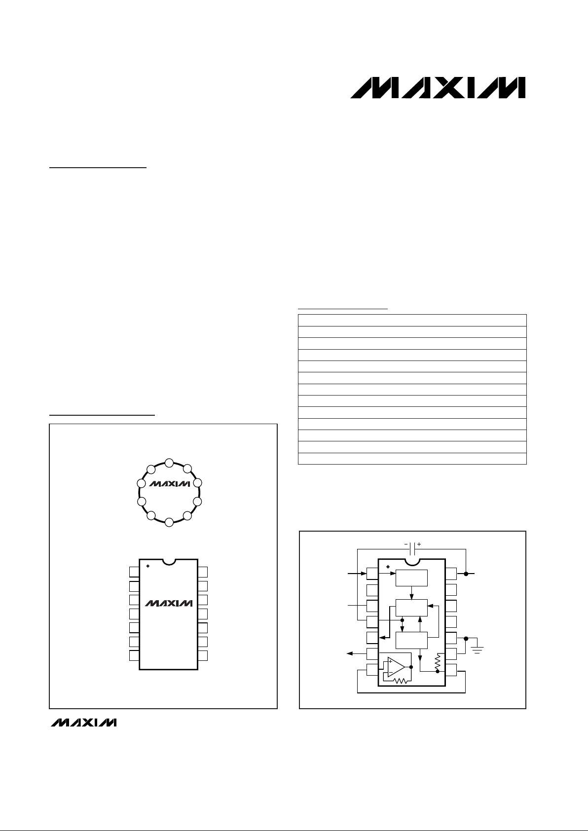
+V
S
N.C.
N.C.
N.C.
COMMON
R
L
I
OUT
V
IN
N.C.
-V
S
C
AV
dB
BUF OUT
BUF IN
MX536A
MX636
DIP
TOP VIEW
MX536A
MX636B
TO-100
8
9
10
1
2
3
4
5
6
7
BUF IN
BUF OUT
dB
C
AV
-V
S
+V
S
I
OUT
R
L
COMMON
V
IN
Pin Configurations
14
13
12
11
10
9
8
1
2
3
4
5
6
7
ABSOLUTE
VALUE
SQUARER
DIVIDER
CURRENT
MIRROR
BUF
V
IN
-V
S
+V
S
V
OUT
C
AV
_________Typical Operating Circuits
19-0824; Rev 2; 3/96
PART
MX536AJC/D
MX536AJCWE
MX536AJD 0°C to +70°C
0°C to +70°C
0°C to +70°C
TEMP. RANGE PIN-PACKAGE
Dice**
16 Wide SO
14 Ceramic
Ordering Information
Ordering Information continued at end of data sheet.
*
Maxim reserves the right to ship ceramic packages in lieu of
CERDIP packages.
**
Dice are specified at TA= +25°C.
MX536AJH
MX536AJN 0°C to +70°C
0°C to +70°C 10 TO-100
14 Plastic DIP
MX536AJQ*
MX536AKCWE 0°C to +70°C
0°C to +70°C 14 CERDIP
16 Wide SO
MX536AKD
MX536AKH 0°C to +70°C
0°C to +70°C 14 Ceramic
10 TO-100
MX536AKN 0°C to +70°C 14 Plastic DIP
Pin Configurations continued at end of data sheet.
Typical Operating Circuits continued at end of data sheet.
MX536AKQ* 0°C to +70°C 14 CERDIP
MX536ASD -55°C to +125°C 14 Ceramic
For free samples & the latest literature: http://www.maxim-ic.com, or phone 1-800-998-8800.
For small orders, phone 408-737-7600 ext. 3468.

MX536A/MX636
True RMS-to-DC Converters
2 _______________________________________________________________________________________
ABSOLUTE MAXIMUM RATINGS
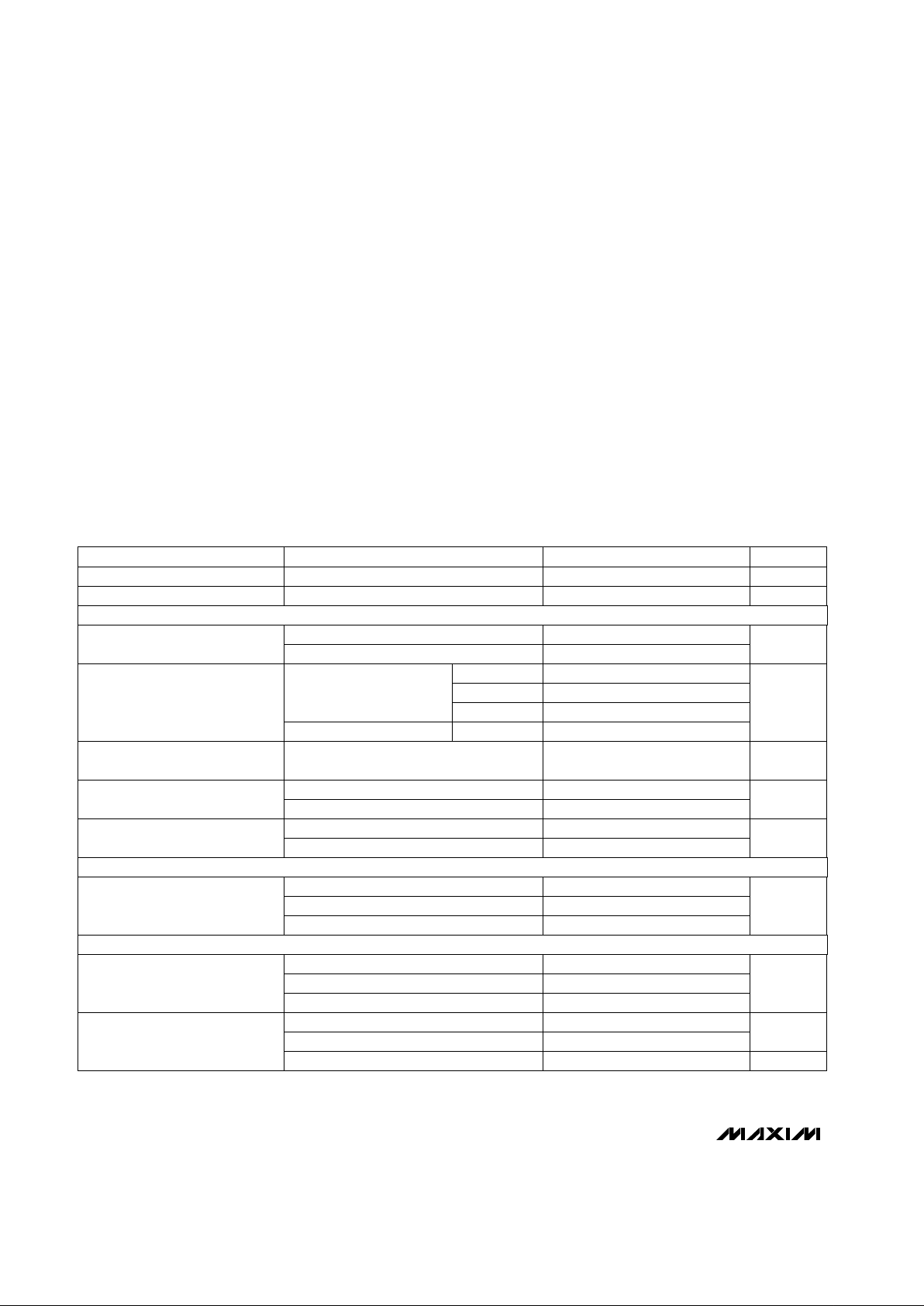
ELECTRICAL CHARACTERISTICS—MX536A
(TA= +25°C, +VS= +15V, -VS= -15V, unless otherwise noted.)
Stresses beyond those listed under “Absolute Maximum Ratings” may cause permanent damage to the device. These are stress ratings only, and functional
operation of the device at these or any other conditions beyond those indicated in the operational sections of the specifications is not implied. Exposure to
absolute maximum rating conditions for extended periods may affect device reliability.
Supply Voltage: Dual Supplies (MX536A)............................±18V
(MX636) .............................±12V
Single Supply (MX536A)...........................+36V
(MX636) .............................+24V
Input Voltage (MX536A).......................................................±25V
(MX636).........................................................±12V
Power Dissipation (Package)
Plastic DIP (derate 12mW/°C above +75°C) ...............450mW
Small Outline (derate 10mW/°C above +75°C)............400mW
Ceramic (derate 10mW/°C above +75°C) ...................500mW
TO-100 metal can (derate 7mW/°C above +75°C)......450mW
Output Short-Circuit Duration........................................Indefinite
Operating Temperature Ranges
Commercial (J, K)...............................................0°C to +70°C
Military (S)......................................................-55°C to +125°C
Storage Temperature Range.............................-55°C to +150°C
Lead Temperature (soldering, 10sec)................................300°C
MX536AJ, AS
T
MIN
to +70°C
+70°C to +125°C
MHz2.3
±3dB Bandwidth
450
kHz
90
120
Bandwidth for 1%
Additional Error (0.09dB)
45 kHz
5
-1.0
Additional Error -0.1
% of
Reading
Specified Accuracy
±2 ±0.1
Total Error, External Trim
(Note 1)
mV ±% of
Reading
±3 ±0.3
±2 ±0.2
Total Error, Internal Trim (Note 1)
mV ±% of
Reading
±5 ±0.5
V
OUT
= [avg. (VIN)2] 1/
2
Transfer Equation
±0.1
Total Error vs. DC Reversal
% of
Reading
±0.2
mV ±% of
Reading/V
±0.1 ±0.01Total Error vs. Supply
Total Error vs. Temperature
mV ±% of
Reading/°C
±0.1 ±0.01
±0.05 ±0.005
±0.1 ±0.005
±0.03 ±0.005
UNITS
MIN TYP MAX
PARAMETER
VIN= 1V
VIN= 100mV
VIN= 10mV
MX536AK
VIN= 1V
VIN= 100mV
MX536AJ, AS
VIN= 10mV
Crest Factor = 7
Crest Factor = 3
Crest Factor 1 to 2
MX536AJ
MX536AK
MX536AS
MX536AK
MX536AS
MX536AJ, AS
CONDITIONS
MX536AK
Figure 3 ms/µF C
AV
25Averaging Time Constant
CONVERSION ACCURACY
ERROR vs. CREST FACTOR (Note 2)
FREQUENCY RESPONSE (Note 3)

MX536A/MX636
True RMS-to-DC Converters
_______________________________________________________________________________________ 3
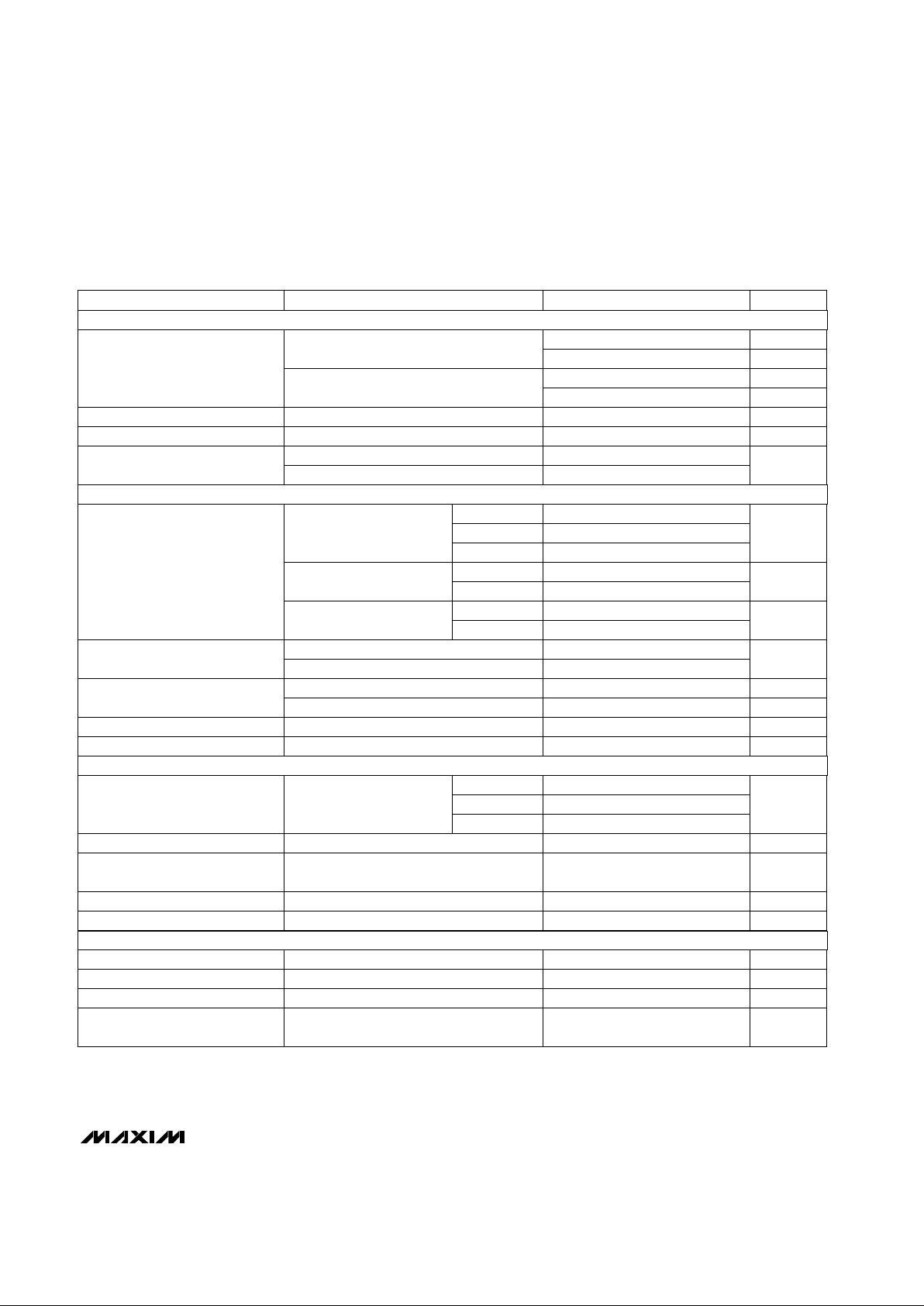
UNITS
MIN TYP MAX
CONDITIONSPARAMETER
V
RMS
0 to 7
±15V Supplies
Continuous RMS Peak Transient
±20 V
PK
0 to 2 V
RMS
Input Signal Range
±5V Supplies
Continuous RMS Peak Transient
±7 V
PK
Safe Input All Supplies ±25 V
PK
Input Resistance 13.33 16.7 20.00 kΩ
MX536AJ, AS 0.8 ±2
mVInput Offset Voltage
MX536AK 0.5 ±1
MX536AJ ±1 ±2
MX536AK ±0.5 ±1TA= +25°C
MX536AS ±2
mV
MX536AJ, AK ±0.1
TA= T
MIN
to T
MAX
MX536AS ±0.2
mV/°C
MX536AJ, AK ±0.1
Offset Voltage
Supply Voltage
MX536AS ±0.2
mV/V
±15V Supplies 0 to 11 12.5
Output Voltage Swing
±5V Supplies 0 to 2
V
Source 5 mA
Output Current
Sink -130 µA
Short Circuit Current 20 mA
Output Resistance 0.5 Ω
MX536AJ ±0.4 ±0.6
dBMX536AK ±0.2 ±0.3Error
VIN= 7mV to 7V
RMS
,
0dB = 1V
RMS
MX536AS ±0.5 ±0.6
Scale Factor -3 mV/dB
Scale Factor TC (Uncompensated) 0.33
% of
Reading/°C
ELECTRICAL CHARACTERISTICS—MX536A (continued)
(TA= +25°C, +VS= +15V, -VS= -15V, unless otherwise noted.)
I
REF
0dB = 1V
RMS
5 20 80 µA
I
REF
Range 1 100 µA
I
OUT
Scale Factor 40 µA/V
RMS
I
OUT
Scale Factor Tolerance ±10 ±20 %
Output Resistance 20 25 30 kΩ
Voltage Compliance
-VSto
(+V
S
- 2.5)
V
INPUT CHARACTERISTICS
OUTPUT CHARACTERISTICS
dB OUTPUT
I
OUT
TERMINAL

MX536A/MX636
True RMS-to-DC Converters
4 _______________________________________________________________________________________
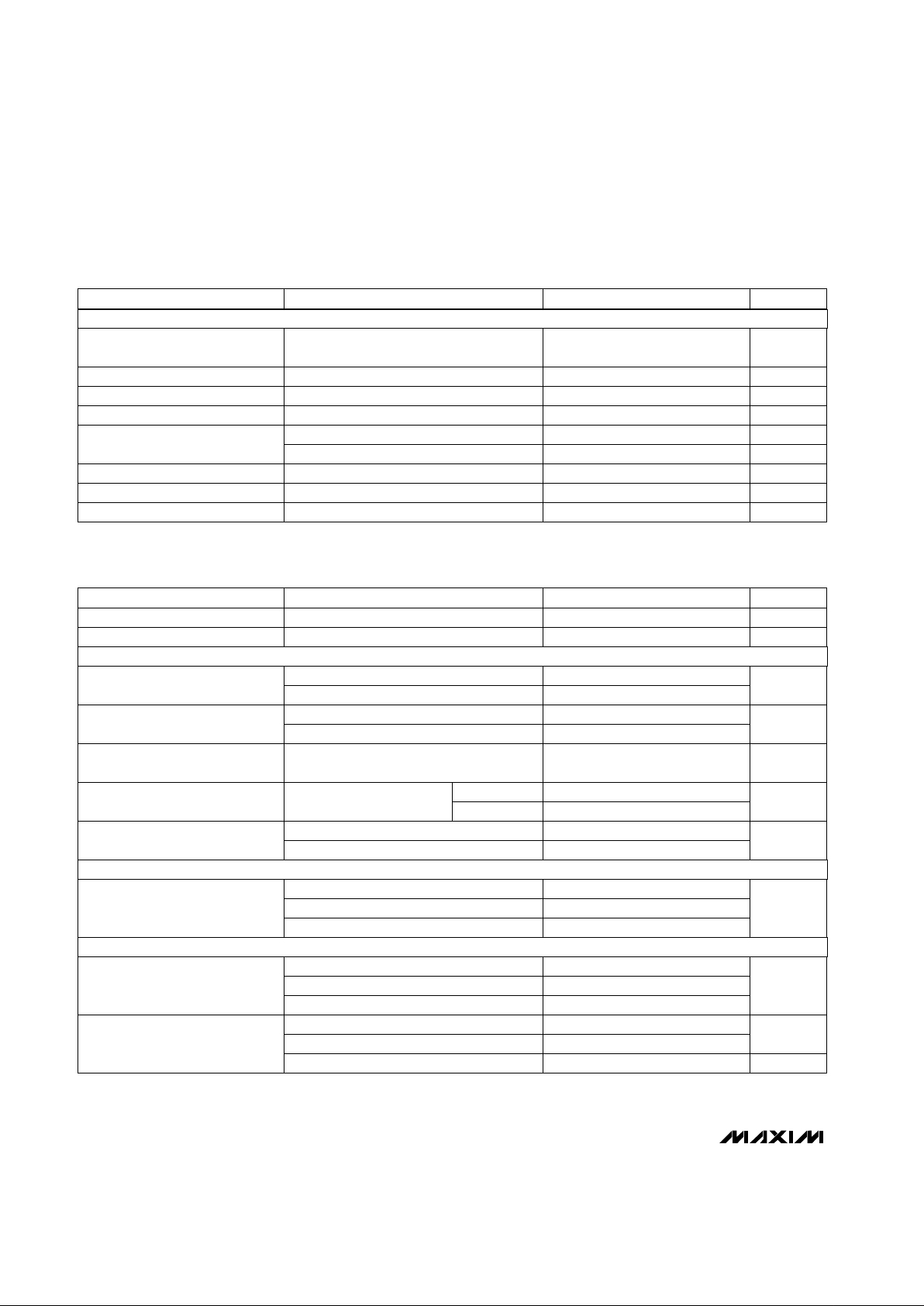
Input Bias Current 20 300 nA
Input Resistance 10
8
Ω
Output Current
Source +5 mA
Sink -130 µA
Short-Circuit Current 20 mA
UNITS
MIN TYP MAX
CONDITIONSPARAMETER
Input and Output Voltage Range
-VSto
(+V
S
- 2.5)
V
Input Offset Voltage RS= 25kΩ
Small-Signal Bandwidth
±0.5 ±4 mV
1 MHz
Slew Rate (Note 4) 5 V/µs
ELECTRICAL CHARACTERISTICS—MX536A (continued)
(TA= +25°C, +VS= +15V, -VS= -15V, unless otherwise noted.)
ELECTRICAL CHARACTERISTICS—MX636
(TA= +25°C, +VS= +3V, -VS= -5V, unless otherwise noted.)
VIN= 200mV
MHz1.5VIN= 200mV
±3dB Bandwidth
900VIN= 100mV
kHz
100VIN= 10mV
130
MX636K
Bandwidth for 1%
Additional Error (0.09dB)
90
VIN= 200mV
kHz
14
VIN= 100mV
MX636J
-0.5
VIN= 10mV
Additional Error -0.2
±% of
Reading
Specified Accuracy
Crest Factor = 6
±0.1 ±0.1
Crest Factor = 3
Total Error, External Trim
(Note 5)
mV ±% of
Reading
±0.3 ±0.1
MX636K
±0.2 ±0.5
MX636J
Total Error, Internal Trim
(Notes 5, 6)
mV ±% of
Reading
±0.5 ±1.0
Crest Factor 1 to 2
V
OUT
= [avg. (VIN)2]
1/2
Transfer Equation
±0.1
Total Error vs. DC Reversal
±% of
Reading
±0.2
mV ±% of
Reading/V
±0.1 ±0.01
MX636J
Total Error vs. Supply
MX636K
Total Error vs. Temperature
(0°C to +70°C)
mV ±% of
Reading/°C
±0.1 ±0.01
±0.1 ±0.005
MX636K
MX636J
UNITSMIN TYP MAXCONDITIONSPARAMETER
BUFFER AMPLIFIER
Figure 3 ms/µF C
AV
25Averaging Time Constant
CONVERSION ACCURACY
ERROR vs. CREST FACTOR (Note 3)
FREQUENCY RESPONSE (Notes 6, 8)
 Loading...