


July 23, 2010
MG3500/MG2580 HD H.264 CODEC
Advance Information
DATA SHEET
For pricing, delivery, and ordering information, please contact Maxim Direct at
1-888-629-4642 or visit Maxim’s website at www.maxim-ic.com.
Document Release 1.4
Document Number: PN1100
Maxim Integrated Products
120 San Gabriel Drive
Sunnyvale, CA 94086
United States
408-737-7600
http://www.maxim-ic.com/support

Copyright © 2010 Maxim Integrated Products
This document contains advanced information and is subject to change without prior notice.
Maxim cannot assume responsibility for use of any circuitry other than circuitry entirely embodied in a
Maxim product. Maxim retains the right to make changes to its products or specifications to improve
performance, reliability or manufactur-ability. All information in this document, including descriptions of
features, functions, performance, technical specifications and availability, is subject to change without notice
at any time. While the information furnished herein is held to be accurate and reliable, no responsibility will
be assumed by Maxim for its use. Furthermore, the information contained herein does not convey to the
purchaser of microelectronic devices any license under the patent right of any manufacturer.
Maxim products are not intended for use in life support products where failure of a Maxim product could
reasonably be expected to result in death or personal injury. Anyone using a Maxim product in such an
application without express written consent of an officer of Maxim does so at their own risk, and agrees to
fully indemnify Maxim for any damages that may result from such use or sale.
is a registered trademark of Maxim Integrated Products, Inc.
All other products or service names used in this publication are for identification purposes only, and may be
trademarks or registered
trademarks of their respective companies. All other trademarks or registered trademarks mentioned herein
are the property of their
respective holders.

1.0: Description 13
1.1: Hardware Overview 14
1.2: Support Tools 18
2.0: Device Overview, Pin Assignments 21
2.1: Naming Conventions 21
2.2: Pinout Diagrams 22
2.3: Pin Descriptions (by Interface) 27
2.4: Power and Ground Pins 52
2.5: Pin List by Power Group 55
2.6: Hookup Recommendations when Interfaces Are
Unused 57
3.0: Device Configuration 67
3.1: Reset 67
3.2: Boot modes for the MMEs and the ARM 67
3.3: Firmware Loader 68
3.4: API Configuration 68
3.5: Pin Multiplexing, GPIOs, etc. 68
3.6: Debug Mode 68
3.7: JTAG ID Register 68
4.0: Device Operating Conditions 71
4.1: Absolute Maximum Ratings 71
4.2: Recommended Operation Conditions 71
4.3: Essential Characteristics 72
4.4: Power Supply Currents for the Different Power
Domains73
4.5: AC Timing 73
5.0: Block Level Operation 97
5.1: Detailed Block Diagram 97
5.2: Reset Logic 98
5.3: Clocks and PLLs 99
5.4: Video Interfaces 103
5.5: Video Scaling 111
5.6: Audio Interfaces 118
5.7: Host Interfaces 120
5.8: Configuration and Status Register (CSR) Defini-
tion 132
5.9: DMA Engine Register Definition 136
5.10: Bitstream Write Register Definition 144
5.11: Special Registers 145
5.12: Memory Interfaces 152
5.13: Serial Interfaces 167
5.14: USB 2.0 On-the-Go Interface 178
5.15: Ethernet Media Access Controller 184
5.16: High-Speed Bitstreams 188
6.0: System Design and Applications 193
6.1: Power Supply Design and Recommendations 193
6.2: Power Supply Sequencing 193
6.3: Reset timing Diagrams 193
6.4: Oscillator Connections, Values and Formulas194
7.0: Ordering Information 197
7.1: Product Information 197
7.2: MG3500 Family Reflow Profile 198
8.0: Packaging Information 201
8.1: Package Diagram 201
8.2: Thermal Data 202
9.0: Marking 203
Maxim Integrated Products Advance Information | 3

Maxim Integrated Products Advance Information | 4
MG3500/MG2580 HD H.264 Codec SoC Data Sheet
Change Log
This section of the data sheet lists the changes that have occurred since the last release. Customers
should be aware that not all releases are public, and therefore they might see gaps in the release
numbering system.
Change Log
Revision Page Section Change
0.18
0.19
0.20 Throughout Made minor changes throughout the book.
0.21 Throughout Valid value for EWait of EM1Config is 1; EM1Cmd register set to 0x00; removal of several reg-
1.0 14 1.1.2 The heading title and description has been changed.
71 4.1 The Core power supply current was changed from 1000 mA. typical to 1000 mA. maximum.
195 6.4.3 A new section was added describing use when only an external clock is used.
43 2.3.8 Specified the resistance of the external USB Bias Current resistor.
43 2.3.9 Modified the timing specification for the SD and MMC Interface.
46 2.3.14 Specified the resistance of the internal pull-up and pull-down resistors
89 4.5.6 Added a new section showing the bitstream timing.
99 5.3 This entire section was re-written to clarify the clock structure.
111 5.5 The definition of the VOUT register was altered.
145 5.11 The specification for the ChipID register was added.
152 5.12 The SDRAM Requirements for Various Profiles table was updated.
184 5.15 Added note regarding the use of an external switch.
190 5.16.5 Updated the Bitstream Register section.
120 5.7.1 Added timing diagrams showing Master Host Interface (MHIF) access timing.
isters, Slave Host Interface; Valid value for EM1 is 0; Corrections to S/PDIF and I2S I/Os; BFifostatus changed to EM1fifostatus.
15 1.1.2 Figure 1-2, only one independent video output is supported.
16 1.1.3 The maximum pixel rate that VIP can process corresponds to the video input of resolution
Throughout Made editorial changes, added definitions, made updates and corrections to several diagrams
1920x1080i at 30 frames per seconds.
and tables throughout the book.
Maxim Integrated Products Advance Information | 5
MG3500/MG2580 HD H.264 Codec SoC Data Sheet
Change Log
Revision Page Section Change
1.1 71 4.1 The core supply voltage has been changed to 1.05v ± 5%.
71 4.2 The minimum, typical, and maximum ranges of the core supply voltage have been re-adjusted.
78 4.5.2 Modified the Video Interface Timing Diagram to incorporate the new t
78 4.5.2 Modified Table 4-7 to indicate that VIDOUT_DATA is an output delay from VID_CLK for the
78 4.5.2 Modified Table 4-8 to indicate that VIDOUT_DATA is an output delay from VID_CLK for the
78 4.5.2 Modified Table 4-9 to indicate that VIDOUT_DATA is an output delay from VID_CLK for the
144 5.10 Made corrections to the bit settings of the BiFiStatus and BiFiConfig registers.
188 5.16.1 Changed the description for the bitstream interface.
190 5.16.5 Removed the old section “High-Speed Bitstream” since it is not supported.
189 5.16.4 Modified Figure 5-39 to show signal BS-DATA is 8 bits long.
189 5.16.4 Changed the definition for Cycle 7 of the waveform diagram.
190 5.16.5 In Bitstream Control 2, removed the unsupported value 1 for BSClkEnMode, BSStopCond,
190 5.16.5 Bitstream Interface Control registers 8, A, and C have been removed.
193 6.2 The second half of the RESETn signal in Figure 6-1has been removed.
201 8.0 Added a new Ordering Information section.
1.2 14 1.1 Added Hardware Description section back.
78 4.5.2 Corrected the note below Table 4-7 to say the clock should be supplied by MG3500.
78 4.5.2 Re-adjusted the t
78 4.5.2 Re-adjusted the t
81 4.5.3 Inverted the AUD_LRCK signal in Figure 4-6.
81 4.5.3 Re-adjusted the shaded area for ETH_RXDV and ETH_RXER signals in Figure 4-10.
81 4.5.3 Modified the description for Figure 4-7.
81 4.5.2 Completely re-drew Figure 4-7.
84 4.5.4 The ETH_TXD signal was corrected to ETH_RXD in Table 4-12.
84 4.5.4 Changed the description for t
86 4.5.4 Changed signals ETH_RXDV and ETH_RXER in Table 4-14.
86 4.5.4 Changed the description for t
88 4.5.4 Changed signals ETH_RXDV and ETH_RXER in Table 4-16.
88 4.5.4 Changed the ETH_RXDV signal in Table 4-16.
81 4.5.3 Re-adjusted the shaded area for ETH_RXDV and ETH_RXER signals in Figure 4-14.
203 9.0 Removed the approval table from the Marking section.
197 7.1.3 Changed the maximum height.
standard definition video interface AC timing values. It also specifies the minimum and maximum timing value in ns.
high definition video interface AC timing values. It also specifies the minimum and maximum
timing value in ns.
high-speed video interface AC timing values. It also specifies the minimum and maximum timing value in ns.
Changed the definition for Cycle 7 of the waveform diagram.
and BSStrobeModeEn signals.
parameter in Figure 4-5.
VCQ
parameter in Figure 4-5.
VIH
to indicate a clock High time in Table 4-12.
ETH
to indicate a clock High time in Table 4-14.
ETH
parameter.
VCQ
6 | Advance Information Maxim Integrated Products

MG3500/MG2580 HD H.264 Codec SoC Data Sheet
Change Log
Revision Page Section Change
1.3 11 “SoC Features” Separated Definitions of output ports for Audio Codecs and Decoders.
11 “SoC Features” Changed SDRAM voltage for DDR_VDD.
13 1.0 Changed the description to provide a summary of both MG3500 and MG2580.
13 1.0 Changed Table 1-1 to specify the features of both MG3500 and MG2580.
13 1.0 Added the slave mode support for MG2580 in Table 1-1.
14 1.1.1 Added the total number of macroblocks required for the H.264 Codec.
14 1.1.2 Changed the description for video processors and interfaces for clarity.
15 1.1.2 Added a note following the text describing Figure 1-2 to indicate that video composition fea-
15 1.1.2 Added a column to Table 1-2 that shows video modes for the video composition.
16 1.1.4 Added a note to indicate the supported formats for video output processor.
16 1.1.7 Modified the description for valid input and outputs for audio interfaces.
17 1.1.12 Removed IDE from the list of external devices that can communicate with the host interface.
18 1.2 Removed the evaluation applications and demonstration product applications supplied by Mo-
19 1.2 Changed the middle box at the bottom of Figure 1-4 to say Mobilygen Software.
31 2.3.3 Added pin descriptions for MG2580 to Table 2-4.
46 2.3.14 Indicated in Table 2-17 that GPIO_2-12, -13, and -15 are not applicable for MG2580.
57 2.6 Indicated in Table 2-24 that VID23_MISO, _MOSI, and _MSS are not available for MG2580
57 2.6 Removed the descriptions for the USB and Ethernet pin names in Table 2-24.
57 2.6 Specified that USB_ADD is recommended for USB_REXT in Table 2-24.
57 2.6 Added a footnote to Table 2-24 that recommends a two-step procedure on how to connect the
71 4.0 Changed the range for the DDR_VDD IO voltage in Table 4-2.
71 4.0 Changed the operating conditions range for DDR_VREF in Table 4-2.
86 4.5.4 Changed ETH_RXER[3:0] to ETH_RXD[3:0] in Figure 4-12.
88 4.5.4 Changed ETH_RXER[1:0] to ETH_RXD[1:0] in Figure 4-14.
125 5.7.1 Specified the bit range for AddrInc and WEn in the “DevConfigAn Register” table.
126 5.7.1 Specified the bit range for RHold in the “DevConfigBn Register” table.
168 5.13.3 Added a new section to describe TWI on MG2580. This includes description as well as a new
169 5.13.2 Changed Figure 5-33 to show that VID23_SDA is not applicable to MG2580.
170 5.13.4 Indicated that this section is about SPI on MG3500. Added a note to imply that V23 SPI port
171 5.13.5 Changed Figure 5-35 to show that VID23_MSS, VID23_MCLK, VID23_MOSI, and
171 5.13.5 Added a new section for SPI on MG2580. This includes descriptions as well as a modified di-
173 5.13.8 Indicated in the Serial I/O Control table that V23_MCLK_AltSeL and V23_MOSI_AltSeL are
173 5.13.8 Indicated in the GPIO 2 Sel that table GPIO_2_12, GPIO_2_13, and GPIO_2_15 fields will
173 5.13.8 Indicated in the GPIO 2 Pull-up Enable table GPIO_2_12, GPIO_2_13, and GPIO_2_15 fields
173 5.13.8 Indicated in the GPIO 2 Pull-up Enable table GPIO_2_12, GPIO_2_13, and GPIO_2_15 fields
197 7.1.3 Removed the part number to order MG2580A2 since this part will no longer be built.
tures are not available when two VIPs are used as inputs.
bilygen.
for VIDEO_PORT 2/3.
USB pins when the USB block is not used on MG3500.
diagram, Figure 5-33.
is not available on MG2580.
VID23_MISO are not applicable to MG2580.
agram, Figure 5-35.
not available on MG2580.
have no effect on MG2580 since GPIO pins are not connected.
will have no effect on MG2580 since GPIO pins are not connected.
will have no effect on MG2580 since GPIO pins are not connected.
Maxim Integrated Products Advance Information | 7
MG3500/MG2580 HD H.264 Codec SoC Data Sheet
Change Log
Revision Page Section Change
1.4 29/30 2.3.2 Changed VID0_PIXCLK and VID1_PIXCLK to IO
40 2.3.6 Added a note for DDR_DQ[31:16] and DDR_DQM[3:] pins are not connected in 16-bit mode
46 2.3.14 Removed alternate functionality for GPIO_6 and GPIO_7
56 2.5 Removed signal USB_VBUS from 3.3V Power Group
71 4.2 Updated ETH_VDD 3.3V +/- 5%
78 4.5.2 Included tVH(min) and tVH(max) in Table 4-7, Table 4-8 and Table 4-9
Added HSYNC, VSYNC, and FRAME signals to the timing diagram. Clarified Setup and Hold
time description with reference to VID_CLK for VID_DATA and VIDOUT_DATA.
81 4.5.3 Updated figure 4-6 as it was not readable in v1.3
87/88 4.5.4 Updated RMII Transmit/Receive Timing Diagram in Figure 4-13 by replacing TXCLK with RX-
103/
104
165 5.12.5 Removed 512 byte page size under NAND flash bulleted item
166 5.12.5 Updated NAND/NOR Flash Interface connected to NOR Flash Memory Figure 5-30
5.4 Included separate block diagrams for MG3500 and MG2580 video paths
CLK. Updated Tables 4-15 accordingly by removing transmit and replacing it with receive
clock.. Changed Min. and Max. values in Table 4-16 for ECYC-ETH_CLK, ETL- Low and ETHHigh Time signal.
8 | Advance Information Maxim Integrated Products
MG3500/MG2580 HD H.264 Codec SoC Data Sheet
Table 1 Pin Name Changes
Old Name New Name Old Name New Name Old Name New Name
ENET_COL ETH_COL HOST_A08 HOST_A8 DDR_D27 DDR_DQ27
ENET_RXD1 ETH_RXD1 HOST_A05 HOST_A5 DDR_D31 DDR_DQ31
ENET_RXERR ETH_RXERR HOST_A06 HOST_A6 DDR_D29 DDR_DQ29
ENET_RXDV ETH_RXDV CF_WAITn CF_WAITn DDR_D30 DDR_DQ30
ENET_CRS ETH_CRS HOST_A02 HOST_A2 DDR_D28 DDR_DQ28
ENET_RXCLK ETH_RXCLK HOST_A09 HOST_A9 DDR_D24 DDR_DQ24
ENET_RXD0 ETH_RXD0 HOST_A07 HOST_A7 DDR_D26 DDR_DQ26
ENET_RXD2 ETH_RXD2 HOST_A03 HOST_A3 DDR_D23 DDR_DQ23
ENET_RXD7 ETH_RXD7 HOST_A04 HOST_A4 DDR_D21 DDR_DQ21
ENET_MDCLK ETH_MDCLK HOST_A01 HOST_A1 DDR_D22 DDR_DQ22
ENET_RXD3 ETH_RXD3 DDR_A03 DDR_A3 DDR_D19 DDR_DQ19
ENET_MDIO ETH_MDIO DDR_A02 DDR_A2 DDR_D20 DDR_DQ20
ENET_RXD6 ETH_RXD6 DDR_A01 DDR_A1 DDR_D16 DDR_DQ16
ENET_RXD4 ETH_RXD4 DDR_A00 DDR_A0 DDR_D17 DDR_DQ17
ENET_TXD0 ETH_TXD0 DDR_A08 DDR_A8 DDR_D18 DDR_DQ18
ENET_RXD5 ETH_RXD5 DDR_A04 DDR_A4 JTAG_TEST TEST
ENET_TXD2 ETH_TXD2 DDR_A07 DDR_A7 RESETn RESETn
ENET_TXD4 ETH_TXD4 DDR_A06 DDR_A6 JTAG_T_SELL JTAG_TAP_SEL
ENET_TXEN ETH_TXEN DDR_A09 DDR_A9 VID1_OCLK VID1_OUTCLK
ENET_TXD3 ETH_TXD3 DDR_D05 DDR_DQ5 VID1_PXCLK VID1_PIXCLK
ENET_TXD5 ETH_TXD5 DDR_D00 DDR_DQ0 VID0_OCLK VID0_OUTCLK
ENET_TXERR ETH_TXER DDR_D07 DDR_DQ7 VID0_PXCLK VID0_PIXCLK
ENET_TXCLK ETH_TXCLK DDR_D04 DDR_DQ4 USB_VDD_D USB_DVDD
ENET_TXD1 ETH_TXD1 DDR_D01 DDR_DQ1 USB_VDDA USB_AVDD
ENET_TXD6 ETH_TXD6 DDR_D06 DDR_DQ6 USB_GNDA USB_AGND
ENET_TXD7 ETH_TXD7 DDR_D02 DDR_DQ2 USB_GNDA USB_AGND
HOST_D08 HOST_D8 DDR_D03 DDR_DQ3 USB_GNDA USB_AGND
HOST_D09 HOST_D9 DDR_D14 DDR_DQ14 USB_VDDA USB_AVDD
HOST_D04 HOST_D4 DDR_D08 DDR_DQ8 USB_VDDAC USB_ACVDD
HOST_D05 HOST_D5 DDR_D15 DDR_DQ15 USB_GNDAC USB_ACGND
HOST_D06 HOST_D6 DDR_DQ9 DDR_DQ9 USB_A_TST USB_ANA_TEST
HOST_D02 HOST_D2 DDR_D10 DDR_DQ10 VID3_FIELD VID23_GPIO
HOST_D03 HOST_D3 DDR_VREF1 DDR_VREF VID3_VSYNC VID_DATA_16
HOST_D07 HOST_D7 DDR_D13 DDR_DQ13 USB_VBUSD USB_D_VBUS
HOST_D01 HOST_D1 DDR_D12 DDR_DQ12 VID3_HSYNC VID_DATA_17
HOST_D00 HOST_D0 DDR_D11 DDR_DQ11 VID2_PXClK VID2_PIXCLK
CF_IACKn CF_INPACKn DDR_D25 DDR_DQ25
Maxim Integrated Products Advance Information | 9

MG3500/MG2580 HD H.264 Codec SoC Data Sheet
10 | Advance Information Maxim Integrated Products
MG3500/MG2580 HD H.264 Codec SoC Data Sheet
SoC Features
HD H.264 Codec
• Dual-Stream High-Definition (HD) or Standard-Definition (SD) H.264 Codecs
• Full-duplex HD or SD operation
• Dual Encode HD or SD or
• Dual Decode HD or SD
• H.264 Codec supports High, Main, and Baseline
profiles
• H.264 Codec up to level 4.1
• H.264 Encoding or decoding up to 1920x1080i
• Programmable resolutions and frame rates
• Multi-stream SD encode or decode
• Video bit rates: 64 kbps – 62.5 Mbps
• Macro-Block Level Adaptive Frame/Field
(MBAFF) support
MPEG-2 Decoder
• HD and SD decoder
• Enables real-time HD MPEG-2 to HD H.264
transcoding
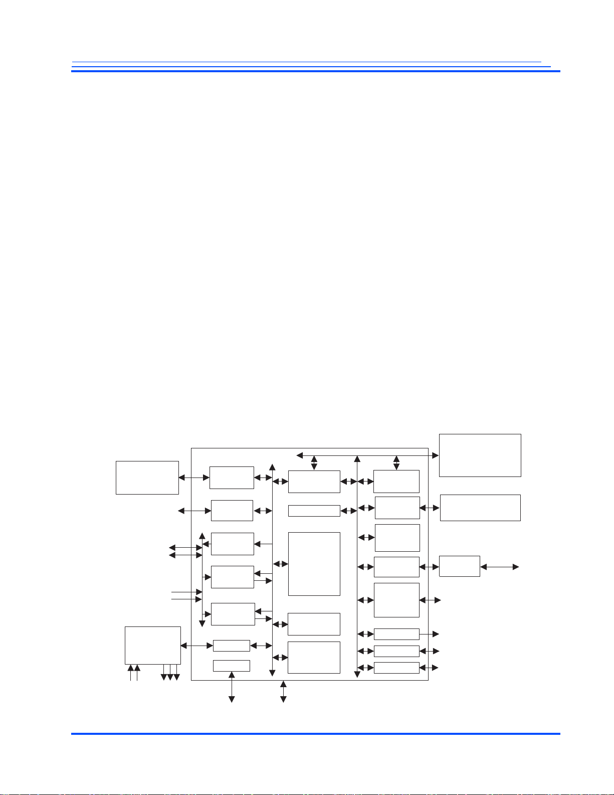
Block Diagram
• Multi-stream SD MPEG-2 decoding
JPEG Codec
• JPEG Encoder and Decoder
• HD or SD MJPEG Support
• Exchangeable Image File Format (EXIF) Support
Audio Codecs & Decoders
• High-fidelity, 2-channel AAC-LC codec
• MPEG-1/2 Audio Layer II codec (MP2)
• MPEG-1/2 Audio Layer I and III decoder (MP1
and MP3)
• Dolby Digital 5.1 decode and down mix
•G.711 Codec
• Flexible bit rates and sample rates
• Additional codecs planned
• One S/PDIF output port
•Two I
2
S Audio input ports and three I2S Audio
output ports
DDR2 SDRAM
(1 or 2 Chips)
High-Speed
Bitstream
Video I/O
ITU-R BT.1120 or
ITU-R BT.656 (2X)
Video Input
ITU-R BT.1120 or
ITU-R BT.656 (2X)
Audio
Codec(s)
Two
Stereo
Inputs
Stereo
Outputs
Three
SDRAM
Controller
Bitstream
I/F
VOP
HD/SD
VIP1
HD/SD
VIP2
HD/SD
I2S
Clocks
XTAL
JTAG
Slave Host/
Bridge
AES/SHA
HD H.264
Codec
HD MPEG2
Decoder
HD JPEG
Codec
Video MME
Audio/
System
MME
Master
Host
SD/MMC
Controller
ARM926
Processor
Ethernet
MAC
USB
Including
a PHY
PWM
Serial I/O
Serial I/O
Master/ Slave Host
I/F/ NAND/NOR/
CF/IDE
16 Data, 23 Address
SDIO/MMC/
CE_ATA
Ethernet
Ethernet
USB 2.0
PWM (3X)
UART (2X)
TWI/SPI (2X)
10/100/GigE
PHY
Maxim Integrated Products Advance Information | 11

MG3500/MG2580 HD H.264 Codec SoC Data Sheet
Video Input Processors (VIPs)
• Flexible direct video inputs
• Two ITU-R BT.1120 parallel interfaces
• Four ITU-R BT.656 parallel interfaces
• Two advanced Video Input Processors (VIPs)
• Digital Image Stabilization
• Smooth Digital Zoom
Video Output Processor (VOP)
• HD or SD output support via ITU-R BT.1120 or
ITU-R BT.656
• Multi-stream decode supports scaled PIP and
multi-channel compositing on video output
• LCD Interface, 16-Bit, 18-bit or 8-bit RGB
• High-quality Video output video scaling
• Two overlay planes with alpha blending and
cursor
• Generates optional external sync signals
Integrated ARM926-EJ Processor
• 240 MHz general purpose processor
• 16 kByte Data Cache
• 16 kByte Instruction Cache
• 16 kByte Scratch Pad Memory
• Three Pulse Width Modulators
• Up to 72 GPIO, 8 dedicated
System
• Core Voltage: 1.05V ± 5%
• SDRAM Voltage: 1.8V ±0.1V
• I/O Voltages: 1.8V, 2.5V, 3.3V ±10%
• On-Chip A/V PLLs driven from single crystal
Power Consumption (MG3500+SDRAM)
• H.264 HD 30fps + AAC Encode 750 mW
Packaging
• 376-ball FPBGA, 18x18mm, 0.8mm pitch,
RoHS compliant
System Connectivity
• 10/100/GigE Ethernet MAC
1
• USB 2.0 On-The-Go (OTG) ports including the
physical layer
• High Speed Bit-stream I/O
• AES and SHA hardware acceleration
Peripheral Interfaces
• Secure Digital (SD), Secure Digital Input/
Output (SDIO), Multi-Media Card (MMC), and
Consumer Electronics AT Attachment (CEATA)
• Compact FLASH, IDE
General Purpose Interfaces
• Two SPI or Two Wire Interface ports
• Three UARTs
1. When both 10/100 and GigE need to be enabled, an
external switch must be installed to select the clock.
Maxim Integrated Products Advance Information | 12

1.0 Description
The Maxim High-Profile H.264 Codecs currently comprises two devices: MG3500 HD H.264 Codec
SoC and MG2580 720p30 H.264 Codec SoC. The MG3500 HD H.264 Codec SoC is a full HD 1080p30
H.264 Codec. It is the ideal choice for any 1080p30 H.264 application as well as multi-channel D1
applications as found in the security surveillance space. Similarly , the MG2580 SoC is the cost-reduced
version of the High-Profile H.264 Codecs that performs 720p30 H.264 and MJPEG encoding
operations. The MG2580 is particularly adapted for both IP camera a nd H.264 webcam designs. Both
chips encompass an ARM926-EJ processor as well as a complete set of System-On-a-Chip (SoC)
features.
Table 1-1 shows the features for each of the devices. Specific information for both of these devices are
covered in this datasheet.
All references to MG3500 throughout this manual also apply to the MG2580 as well unless stated
otherwise.
Table 1-1 MG3000 Family of High-Definition H.264 Codecs
Standard Definition Codec
High Definition H.264 Codec 1080p30 720p30
MPEG-2 Decoder
JPEG Codec
Video Input Ports Supported (8-bit or 16-bit) 2 1
Frame Multiplexed Video Inputs 4 –
Video Input Processors 2 2
Video Output Ports Supported (8-bit or 16-bit)
Video Output Prcessors 1 1
Audio Input Ports 2 1
Audio Codecs and Decoders
High-Speed Bitstream I/O –
Embedded ARM926-EJ Processor
Master Mode Operation
Slave Mode Operation
Embedded 10/100/GigE Ethernet MAC
USB On-The-Go including Physical Layer
SD, SDIO, MMC, CE-ATA Peripheral Interface
Compact Flash
32-Bit SDRAM Interface
SPI or Two-Wire Interface 3 2
UARTs 3 3
Pulse Width Modulators 3 3
GPIO, Shared 64 61
GPIO, Dedicated 8 8
1.The MG2580 supports 8-bit output only. MG3500 can support an 8-bit or 16-bit output.
MG3500/MG2580 HD H.264 Codec SoC Data Sheet
Feature MG3500 MG2580
1
11
Maxim Integrated Products Advance Information | 13

MG3500/MG2580 HD H.264 Codec SoC Data Sheet
1.1 Hardware Overview
This section provides an overview of each of the blocks in the MG3500 SoC. See “Block Diagram” on
page 11.
1.1.1 Video Codecs
The MG3500 SoC includes efficient hardware implementations of two HD encoders and three HD
decoders:
• H.264 Encoder/Decoder
•MPEG2 Decoder
• JPEG/MJPEG Encoder/Decoder
As shown in Figure 1-2, the H.264 Codec, MPEG2 Decoder and JPEG/MJPEG Codec are implemented
as separate elements in order to support real time trans-coding from one format to another.
The H.264 Codec hardware pipeline allows the highest processing power at the lowest power
consumption to support all of the H.264 tools for the High, Main, and Baseline profiles. The processing
power that enables HD Encoding or Decoding can also be applied to Encoding or Decoding multiple
reduced resolution or SD streams.
The H.264 Codec is capable of encoding or decoding up to 1920 pixels per line (horizontal) and up to
2000 lines (vertical) as long as the total number of 16x16 macroblocks does not exceed 8192 and the
macroblocks per second does not exceed 244800.
The HD MPEG2 Decoder is also capable of decoding up to a maximum of 1920 pixels per line
(horizontal) and 2000 lines (vertical). It does not have encoding capabilities.
The JPEG/MJPEG Codec is also capable of decoding up to a maximum of 1920 pixels per line
(horizontal) and 2000 lines (vertical) for real time video, but in addition, it can encode or decode up to
8k by 8k still images that reside in the memory.
1.1.2 Video Processors and Interfaces
As shown in Figure 1-2, the MG3500 SoC video path has two Video Input Processors (VIP: VIP1 and
VIP2) and one Video Output Processor (VOP).
The Codec has two 8-bit video inputs (VID0 and VID1) that can be used either as two individual 8-bit
ITU-R BT 656 video inputs or a single 16-bit ITU-R BT 1 120 video input fo r HD inputs from an HDMI
receiver or other HD input.
Additionally, the Codec provides two bi-directional ports (VID2 and VID3) that can be used either as
an HD input or as an output (one 8-bit or one 16-bit output).
These bi-directional ports can be clocked at higher frequency to support non-standard video interfaces.
These two 8-bit interfaces can be combined to create a single 16-bit HD ITU-R BT 1120 interface.
The bi-directional video ports can also be used to drive an LCD display in one of two modes. As an
standard output, it can drive an 8-bit RGB LCD interface or it can be used as a 16-bit HD output. Two
additional bits are available to drive an 18-bit RGB LCD interface.
Each video input supports independent clocks and synchronization signals. The clock frequency can be
driven over 100 MHz in order to support non-standard video inputs including HD sensors with 8- bit
interfaces.
14 | Advance Information Maxim Integrated Products
Memory
Controller
VIP2
180 MHz
VIP1
180 MHz
VOP
125 MHz
Two 8-Bit
Video I/Os
125 MHz
Maximum
Memory
Two 8-Bit
Video Inputs
125 MHz
Maximum
Video Portion of the MG3500 and MG3264 Codec
From Memory
RGB or
YUV 4:2:2
Video
Codecs
High Definition
H.264 Codec
High Definition
MPEG2 Decoder
High Definition
JPEG Codec
VID0_D[7:0]
VID1_D[7:0]
VID2_D[7:0]
VID3_D[7:0]
32-bit Data
MG3500/MG2580 HD H.264 Codec SoC Data Sheet
Figure 1-2 Block Diagram of the Video Input Section
The two VIPs and one VOP provide the capability of processing two independent video inputs and one
independent video output. Together with the flexible Video Interfaces described above, the modes
shown in Table 1-2 are supported.
Note: Video composition features, such as memory-based scaling or merging multiple videos into one
screen are not available when two VIPs are both used as inputs.
Table 1-2 Video Modes
Video Mode Video Inputs Video Outputs Video Composition
11 HD 1 HD Yes
2 1 HD 1 SD Yes
3 2 HD None Not Available
4 2 SD 1 HD Not Available
5 1 SD + 1 HD 1 SD Not Available
6 2 SD 1 SD Not Available
Note: The HD output can be used as an 18-bit LCD interface and an SD output can be used as an 8-bit
LCD interface.
Maxim Integrated Products Advance Information | 15
MG3500/MG2580 HD H.264 Codec SoC Data Sheet
1.1.3 Video Input Processor
There are two identical Video Input Processors (VIPs) that perform high quality scaling, chroma and
gamma adjustment, filtering, and the extraction of video analytics. The maximum pixel rate that the VIP
can process corresponds to video input of resolution 1920x1080i at 30 frames per seconds.
1.1.4 Video Output Processor
The Video Output Processor (VOP) performs high quality scaling of un-compressed video, overlays it
with two graphic planes, performs gamma and chroma adjustment, overlays a hardware cursor, and
outputs the combined video to a video port. Each graphic plane can be from 1 to 32 bits. Graphic planes
using less than eight bits use a Look-Up Table (LUT).
Note: Some formats may not be possible depending on the output resolution and available system memory
bandwidth. For example 32 bits/pixel modes are not possible for 1080i60 resolution output.
Table 1-3 Video Output Modes
Mode Bits/Pixel Format Mode Bits/Pixel Format
0 1 Indexed 16 16 RGB 4:4:4
1 1 Grayscale 17 16 RGB 4:4:4:4
2 2 Indexed 18 16 RGB 5:5:5
3 2 Grayscale 19 16 RGB 5:5:5:1
4 4 Indexed 20 16 RGB 5:6:5
5 4 Grayscale 21 16 RGB 5:6:4:1
6 8 Indexed 24 32 RGB 8:8:8
7 8 Grayscale 25 32 RGB 8:8:8:8
The video output can be either be YCbCr via an 8-bit ITU-R BT 656 interface, YCbCr via a 16-bit
ITU-R BT 1120 interface, RGB via an 8-bit interface, or RGB via an 18-bit interface. In some of the
output modes, the MG3500/MG2580 HD H.264 Codec SoC is also capable of generating optional
external sync signals.
1.1.5 Video Multi-Media Engine
The V ideo Multi-Media Engine (MME) is a proprietary Reduced Instruction Set Computer (RISC) that
has been optimized for single cycle context switching and low power. The Video MME controls all
aspects of the VIPs, Video Cores, and the VOP (see the MG3500/MG2580 HD H.264 Codec SoC Block
Diagram on page 3 for more information).
1.1.6 Audio Multi-Media Engine
The Audio MME implements all audio Codecs in firmware.
1.1.7 Audio Interfaces
There are two I2S inputs, three I2S outputs, and one S/PDIF output. One of the two I2S inputs is
associated with one of the audio clocks. The other audio input, the three audio outputs, and the S/PDIF
output must share a common clock and sample rate. The three I
2
S outputs and the S/PDIF output must
also share a common format.
16 | Advance Information Maxim Integrated Products

MG3500/MG2580 HD H.264 Codec SoC Data Sheet
1.1.8 SDRAM
The MG3500/MG2580 HD H.264 Codec SoC has a high performance memory subsystem that uses
either a 16- or 32-bit wide external SDRAM. The SDRAM is DDR2, and runs up to 264 MHz.
1.1.9 ARM926-EJ
The MG3500/MG2580 HD H.264 Codec SoC has an embedded ARM926-EJ processor that runs at
speeds up to 240 MHz. This processor is not used for Audio or Video Codec functions, so it is
completely available to implement any required system level functions. Mobilygen provides Codec and
Data Streaming APIs under Linux 2.6.20.
1.1.10 Ethernet Media Access Controller
The Ethernet MAC supports 10/100/1000 Mbps Ethernet interfaces.1 This is typically connected to an
external Physical Layer (Phy) device but can also be connected directly to Ethernet switches that
support Reverse MII interfaces.
1.1.11 USB 2.0
The USB interface is USB 2.0, High-Speed with the ability to operate as Device, Host, or On-The-Go
(OTG) at speeds of up to 480 MHz. The USB interface includes the Physical Layer.
1.1.12 FLASH, IDE and Host Interface
The host interface can be used to communicate to external devices including NOR FLASH, NAND
FLASH, and COMPACT FLASH, as well as other devices.
1.1.13 SD/MMC Interface
The SD/MMC interface is designed to support Secure Digital (SD), Secure Digital Input/Output
(SDIO), Multi-Media Card (MMC), and Consumer Electronics A T Attachment (CE-AT A) devices. This
four-bit wide interface supports up to a 25 MHz clock rate (100 Mbits/sec. transfer rate).
1.1.14 AES and SHA Hardware Acceleration
The MG3500 SoC design includes hardware acceleration for the Advanced Encryption Standard (AES)
and Secure Hashing Algorithm (SHA). The AES accelerator supports CBC, CTR, ECB, and CCM
modes with 128, 192, and 256 bit keys for secure data storage and transmission. The SHA accelerator
supports the creation of 128, 224, and 256 bit digests for Digital Signatures and Digital Time Stamps.
1.1.15 Serial and Misc. IO
The MG3500 SoC has several UARTs for communication, Pulse Width Modulators (PWMs) for
control, I
2
C-compatible T wo W ire Interfaces (TWIs) for device control, and Serial Peripheral Interfaces
(SPIs) for device control.
The MG3500 SoC also has eight dedicated General Purpose Input/O utput (GPIO) pins and up to 64
shared GPIO pins that can be used for system control. The shared GPIO pins are multiplexed with other
functions and are only available when the primary function for the pin is not being used. For example,
if your design does not require a SPI interface (see “SPI/Bitstream Interface Timing” on page 89), the
four pins dedicated to that interface can be used as GPIO pins.
1. When both 10/100 and GigE need to be enabled, an external switch must be installed to select the clock.
Maxim Integrated Products Advance Information | 17
MG3500/MG2580 HD H.264 Codec SoC Data Sheet
Customer Production
Applications or Mobilygen
Demonstrations, Web-
based Applications,
Command Line Shell
Applications, and Plug-ins
APPLICATION SOFTWARE
Built on Mobilygen's Demonstration Product Applications,
Web-based, Command Line Shell, and Plug-in Modules
Mobilygen Software can
run on an Embedded
ARM926 or an External
Processor
Mobilygen CODECs
and Silicon
SUPPORT SOFTWARE
Production Ready Drivers and APIs
CODECs and SILICON
Production Ready Firmware and Silicon
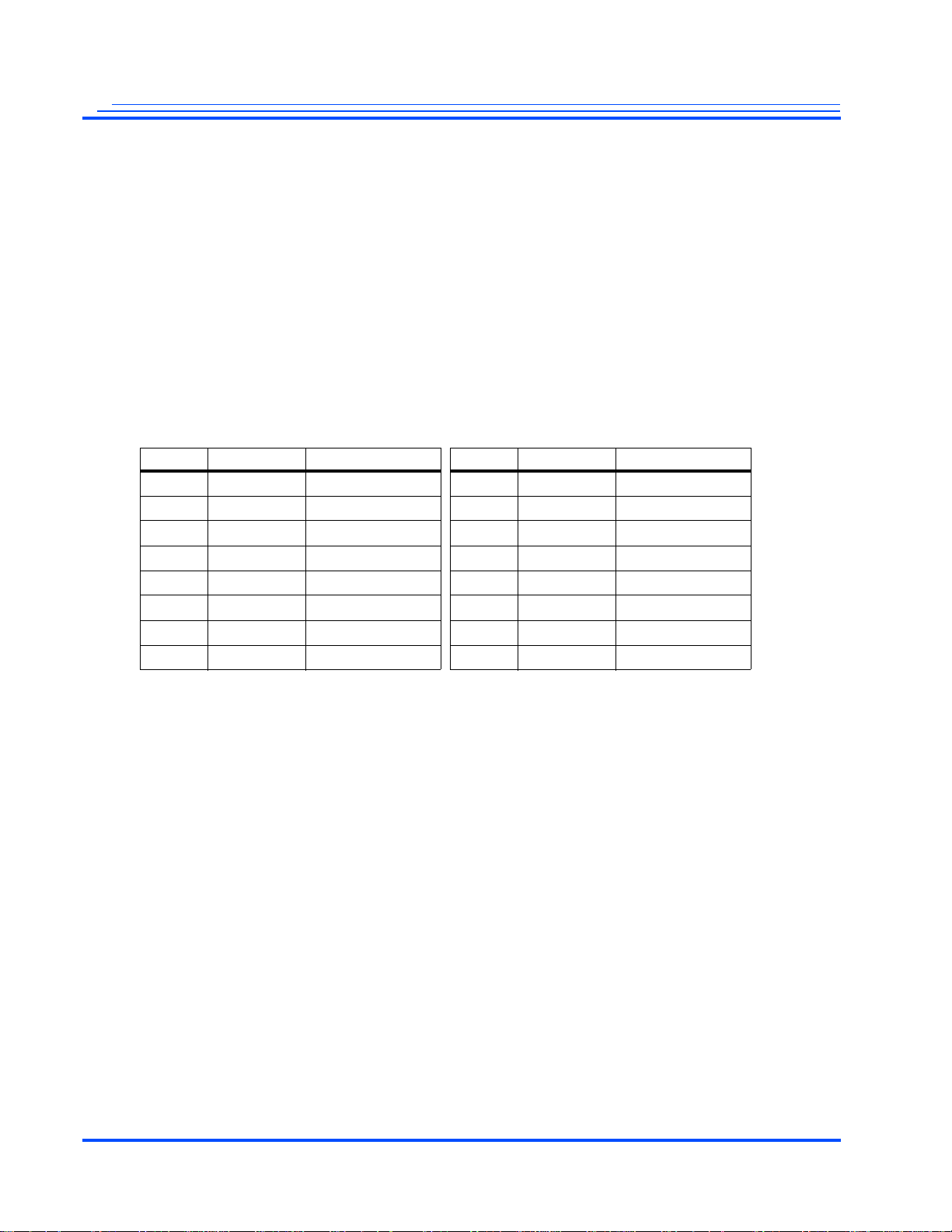
1.2 Support Tools
This section provides an overview of the software and hardware development tools that are available to
support the part.
Figure 1-3 Software Architecture
The Mobilygen-developed MG3500 SoC software is developed for Linux 2.6.20. Mobilygen supplies
these APIs and Drivers:
•Codec API
• qHAL Hardware Abstraction Layer
• Data Streaming API
• On-Chip Device Drivers
Figure 1-4 shows an expanded version of Figure 1-3 that has all of the elements of the system software
included. In this figure:
• Blue boxes are applications, firmware, drivers, and silicon supplied by Mobilygen.
• Green boxes are applications that are available from third-party vendors (public domain or Linux
vendors)
• White boxes are customer-written applications
18 | Advance Information Maxim Integrated Products
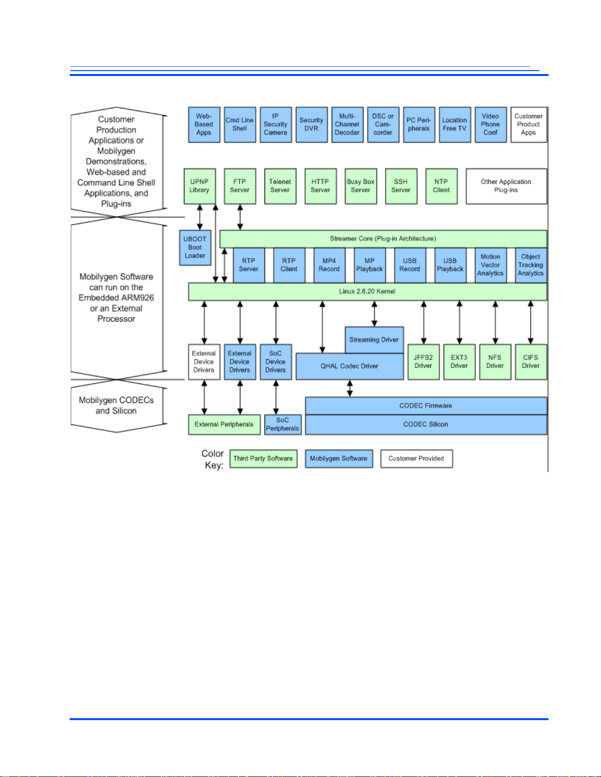
MG3500/MG2580 HD H.264 Codec SoC Data Sheet
Figure 1-4 Software Elements
Note: As shown in Figure 1-4, the Mobilygen supplied drivers and higher-level functions (the lower
two-thirds of Figure 1-4) are production ready and fully supported by Mobilygen. The Customer
Production Applications and Mobilygen Demonstration programs (the upper third of Figure 1-4) are
available for customers to use as an advanced starting point, but are not production ready.
Maxim Integrated Products Advance Information | 19

MG3500/MG2580 HD H.264 Codec SoC Data Sheet
20 | Advance Information Maxim Integrated Products

2.0 Device Overview, Pin Assignments
2.1 Naming Conventions
The MG3500 SoC has both signal and power connections. Each signal has a unique name. Power
connections do not necessarily have unique names.
The signals are organized by signal groups. The signal names typically have two parts separated by an
underscore. When that is the case the first part represents the name of the signal group a nd the second
part defines the function within that group. The signal gr oup names do not have an underscore in them,
so the first underscore separates the signal group name from the function name. The function name may
have an underscore in it. Signals that are active low end with a lower case ‘n’.
Power connection names also have two parts separated by an underscore. The first part represents the
power domain, and the second part represents the power type.
All pins have a Primary function, and the name that is assigned to the pin reflects that primary function.
Many of the pins have an Alternate (ALT) function that can be used if the primary function is not used.
Some pins are capable of being used as General Purpose I/O pins (GPIO) is neither their primary or their
secondary functions are being used. These pins are available for customer-assigned uses.
MG3500/MG2580 HD H.264 Codec SoC Data Sheet
The pinout diagrams and tables in this section list the pins by their Primary name. The pinout tables also
show the Alternate and GPIO capabilities of the pins if any are assigned to them.
Maxim Integrated Products Advance Information | 21
MG3500/MG2580 HD H.264 Codec SoC Data Sheet
RESET Group
AUDIO Power
1234567891011
A
B
C
D
E
F
G
H
J
K
L
12 13 14 15 16 17 18 19 20 21 22
M
N
P
R
T
U
V
W
Y
AA
AB
12345678910111213141516171819202122
A
B
C
D
E
F
G
H
J
K
L
M
N
P
R
T
U
V
W
Y
AA
AB
JTAG Group
AUDIO Power
AUDIOGroup
AUDIO Power
DDR Group
DDR Power
CF Group
HOST Power
HOST Group
HOST Power
HOST Group
HOST Power
PWM Group
HOST Power
UART Group
HOST Power
TWI Group
HOST Power
DDR Group
DDR Power
VID01 Group
VID01 Power
VID23 Group
VID23 Power
USB Group
USB Power
CONFIG Group
VID01 Power
ETH Group
ETH Power
SPI Group
HOST Power
SDMMC Group
HOST Power
GPIO Group
HOST Power
HOST
CS0n
HOST
CS5n
GPIO3GPIO2GPIO
1
GPIO7GPIO6GPIO
5
GPIO
0
GPIO
4
UART0
RTS
UART0
TXD
UART1
RXD
UART0
CTS
UART0
RXD
UARTD
TXD
UARTD
RXD
UART1
TXD
TWI0
SDA
PWM2PWM1PWM
0
HOST
D12
HOST
D13
HOST
D14
HOSTD8HOSTD9HOST
D10
HOSTD4HOSTD5HOST
D6
HOSTD2HOSTD3HOST
WEn
HOSTD1HOST
D_EN
HOST
WAIT
HOST
D15
HOST
D11
HOST
D7
CF
INPACKn
HOST
A12
HOST
ALEnCFIORDnCFBVD2
HOST
INTnCFIOWRnCFCD1
HOST
A11
HOST
A10
HOST
A8
CF
RESETCFREGn
HOST
A6
CFWPHOSTA5HOST
A2
HOST
A7
HOST
A3
HOSTD0HOST
REn
HOST
DMARQ
HOSTWPCF
BVD1CFCD2CFWAITn
HOSTA4HOST
A1
HOST
A22
HOST
A21
HOST
VDD
HOST
A20
HOST
A19
CORE
VDD
HOST
A18
HOST
VDD
HOST
A17
HOST
A16
HOST
VDD
HOST
VDD
HOST
VDD
HOST
A15
HOST
A14
HOST
A13
HOST
VDD
HOST
A9
CORE
GND
HOST
GND
HOST
GND
HOST
GND
HOST
GND
HOST
GND
HOST
GND
HOST
GND
HOST
CS4n
HOST
CS3n
HOST
CS2n
HOST
CS1n
CLK
IN
SDMMCCDSDMMC
D1
SDMMCWPSDMMC
D0
SDMMCD3SDMMC
CLK
DDR
BA0
DDR
WEn
DDRA1DDR
BA1
DDR
CASn
DDRA2DDR
A10
DDR
RASn
DDR
CKE
DDR
DQ5
DDR
DQ7
DDR
A12
DDRA6DDR
DQ0
DDRA8DDRA7DDR
A9
DDR
DQS0n
DDR
DQS0
DDR
DQ1
DDR
DQ3
DDR
DQ4
DDR
DQ2
SDMMCD2SDMMC
CMD
DDRA3DDRA0DDR
CSn
DDRA5DDRA4DDR
A11
DDR
VREF
DDR
DQ6
DDR
VDD
DDR
VDD
DDR
VDD
DDR
VDD
DDR
PADHI
DDR
DQ31
DDR
PADLO
DDR
DQ25
DDR
VDD
DDR
DQS1n
DDR
DQM1
DDR
DQ9
DDR
DQS1
DDR
DQ30
DDR
DQ28
DDR
DQ27
DDR
DQ29
DDR
CLK1
DDR
CLK1n
DDR
CLK0
DDR
CLK0n
HOST
VDD
CORE
VDD
PLL
VDD
CORE
VDD
CLK
SEL
CORE
VDD
DDR
VDD
CORE
VDD
DDR
VDD
DDR
VDD
DDR
DQ14
DDR
DQ15
DDR
DQM0
DDR
DQ8
DDR
DQ13
DDR
DQ11
DDR
DQ10
DDR
DQ12
CORE
GND
CORE
GND
CORE
GND
CORE
GND
DDR
GND
DDR
GND
DDR
GND
DDR
GND
DDR
GND
DDR
GND
DDR
GND
CLK Grp
HOST Pwr
JTAG
TDO
TEST
JTAG
TAP_SEL
JTAG
TDI
JTAG
TRSTn
JTAG
TCK
JTAG
TMS
CFG
HOST1
CFG
HOST0
VID0
FIELD
VID0
OUTCLK
VID0
PIXCLK
VID0
VSYNC
VID0
HSYNC
VID0
D0
VID0D1VID0D5VID1
PIXCLK
VID0D2VID0
D6
VID1
OUTCLK
VID0D3VID0D7VID1
VSYNC
VID0D4VID1
FIELD
VID1
HSYNC
VID1D0VID1D4VID1
D7
VID1D1VID1D5VID01
MOSI
VID1D2VID1D6VID01
MCLK
VID1D3VID01
MSS
VID01
MISO
RESETn
CFG
0
VID01
VDD
AUD1
MCLK
AUD1
BCK
AUD1
LRCK
AUD1
IDAT
CORE
VDD
VID01
VDD
VID01
VDD
CORE
VDD
AUD
VDD
CORE
VDD
DDR
VDD
DDR
VDD
AUD
VDD
AUD0
ODAT1
AUD0
ODAT2
AUD0
MCLK
AUD0
BCK
DDR
VDD
DDR
DQ18
DDR
DQM2
DDR
DQ19
DDR
DQ20
DDR
DQM3
DDR
DQ23
AUD0
IDAT
AUD0
SPDIF
AUD0
LRCK
AUD0
ODAT0
DDR
DQS2n
DDR
DQS2
DDR
DQ17
DDR
DQ16
DDR
DQ21
DDR
DQ22
DDR
VDD
DDR
DQ26
DDR
DQ24
DDR
DQS3n
DDR
DQS3
CORE
GND
DDR
GND
DDR
GND
DDR
GND
CORE
GND
CORE
GND
VID01
GND
AUD
GND
AUD
GND
DDR
GND
DDR
GND
VID01
GND
CFG
3
CFG
2
VID23
MCLK
VID2D0VID2D1VID2D4VID2D6VID2
PIXCLK
ETH
RXERR
VID23
MISO
VID2D2VID2D5VID2D7VID2
FIELD
ETH
RXCLK
ETH
RXDV
VID23
MOSI
VID2D3VID2
VSYNC
VID23
D16
ETH
RXD7
ETH
RXD2
ETH
RXD1
VID23
MSS
VID2
HSYNC
VID3
D1
VID3D2VID3D6USB
XIN
USBDMUSB
DP
VID3D3VID3D7USBXOUSB
VBUS
USB
ID
VID3D0VID3
D4
USB
D_VBUS
USB
REXT
VID3D5VID23
D17
VID23
GPIO
USB
ANA_TST
ETH
RXD6
ETH
RXD3
ETH
RXD0
ETH
COL
ETH
RXD5
ETH
RXD4
ETH
MDCLK
ETH
CRS
ETH
TXEN
ETH
TXD4
ETH
TXD0
ETH
MDIO
ETH
TXERR
ETH
TXD5
ETH
TXD3
ETH
TXD2
ETH
TXD7
ETH
TXD6
ETH
TXCLK
ETH
TXD1
TWI0
SCL
SPI
MOSI
SPI
MCLK
SPI
MSS1
VID23
VDD
VID23
VDD
ETH
VDD
ETH
VDD
USB
AGND
USB
AGND
USB
AGND
USB
ACGND
CFG
1
VID23
VDD
USB
AVDD
USB
AVDD
USB
ACVDD
USB
DVDD
SPI
MISO
CORE
VDD
SPI
MSS0
ETH
GND
ETH
GND
VID23
GND
VID23
GND
CORE
GND
CORE
GND
USB
DGND
VID23
GND
VID01
GND
CORE
VDD
2.2 Pinout Diagrams
Figure 2-1 shows a map of all the signal positions.
22 | Advance Information Maxim Integrated Products
Figure 2-1 Map of all the MG3500 SoC Signal Positions (Top View)
MG3500/MG2580 HD H.264 Codec SoC Data Sheet
1234567891011
A
B
C
D
E
F
G
H
J
K
L
CFG
3
CFG
2
VID23
MCLK
VID2D0VID2D1VID2D4VID2D6VID2
PIXCLK
ETH
RXERR
VID23
MISO
VID2D2VID2D5VID2D7VID2
FIELD
ETH
RXCLK
ETH
RXDV
VID23
MOSI
VID2D3VID2
VSYNC
VID23
D16
ETH
RXD7
ETH
RXD2
ETH
RXD1
VID23
MSS
VID2
HSYNC
VID3
D1
VID3D2VID3D6USB
XIN
USBDMUSB
DP
VID3D3VID3D7USBXOUSB
VBUS
USB
ID
VID3D0VID3
D4
USB
D_VBUS
USB
REXT
VID3D5VID23
D17
VID23
GPIO
USB
ANA_TST
ETH
RXD6
ETH
RXD3
ETH
RXD0
ETH
COL
ETH
RXD5
ETH
RXD4
ETH
MDCLK
ETH
CRS
ETH
TXEN
ETH
TXD4
ETH
TXD0
ETH
MDIO
ETH
TXERR
ETH
TXD5
ETH
TXD3
ETH
TXD2
ETH
TXD7
ETH
TXD6
ETH
TXCLK
ETH
TXD1
TWI0
SCL
SPI
MOSI
SPI
MCLK
SPI
MSS1
VID23
VDD
VID23
VDD
ETH
VDD
ETH
VDD
USB
AGND
USB
AGND
USB
AGND
USB
ACGND
CFG
1
VID23
VDD
USB
AVDD
USB
AVDD
USB
ACVDD
USB
DVDD
SPI
MISO
CORE
VDD
SPI
MSS0
ETH
GND
ETH
GND
VID23
GND
VID23
GND
CORE
GND
CORE
GND
USB
DGND
VID23
GND
VID01
GND
1234567891011
A
B
C
D
E
F
G
H
J
K
L
CFG
3
CFG
2
VID23
MCLK
VID2D0VID2D1VID2D4VID2D6VID2
PIXCLK
ETH
RXERR
VID23
MISO
VID2D2VID2D5VID2D7VID2
FIELD
ETH
RXCLK
ETH
RXDV
VID23
MOSI
VID2D3VID2
VSYNC
VID23
D16
ETH
RXD7
ETH
RXD2
ETH
RXD1
VID23
MSS
VID2
HSYNC
VID3
D1
VID3D2VID3D6USB
XIN
USBDMUSB
DP
VID3D3VID3D7USBXOUSB
VBUS
USB
ID
VID3D0VID3
D4
USB
D_VBUS
USB
REXT
VID3D5VID23
D17
VID23
GPIO
USB
ANA_TST
ETH
RXD6
ETH
RXD3
ETH
RXD0
ETH
COL
ETH
RXD5
ETH
RXD4
ETH
MDCLK
ETH
CRS
ETH
TXEN
ETH
TXD4
ETH
TXD0
ETH
MDIO
ETH
TXERR
ETH
TXD5
ETH
TXD3
ETH
TXD2
ETH
TXD7
ETH
TXD6
ETH
TXCLK
ETH
TXD1
TWI0
SCL
SPI
MOSI
SPI
MCLK
SPI
MSSI
VID23
VDD
VID23
VDD
ETH
VDD
ENET
VDD
USB
AGND
USB
AGND
USB
AGND
USB
ACGND
CFG
1
VID23
VDD
USB
AVDD
USB
AVDD
USB
ACVDD
USB
DVDD
SPI
MISO
CORE
VDD
SPI
MSSO
ETH
GND
ETH
GND
VID23
GND
VID23
GND
CORE
GND
CORE
GND
USB
DGND
VID23
GND
VID01
GND
12 13 14 15 16 17 18 19 20 21 22
A
B
C
D
E
F
G
H
J
K
L
JTAG
TDO
TEST
JTAG
TAP_SEL
JTAG
TDI
JTAG
TRSTn
JTAG
TCK
JTAG
TMS
CFG
HOST1
CFG
HOST0
VID0
FIELD
VID0
OCLK
VID0
PIXCLK
VID0
VSYNC
VID0
HSYNC
VID0
D0
VID0D1VID0D5VID1
PIXCLK
VID0D2VID0D6VID1
OCLK
VID0D3VID0D7VID1
VSYNC
VID0D4VID1
FIELD
VID1
HSYNC
VID1D0VID1D4VID1
D7
VID1D1VID1D5VID01
MOSI
VID1D2VID1D6VID01
MCLK
VID1D3VID01
MSS
VID01
MISO
RESETn
CFG0CORE
VDD
VID01
VDD
AUD1
MCLK
AUD1
BCK
AUD1
LRCK
AUD1
IDAT
CORE
VDD
VID01
VDD
VID01
VDD
CORE
VDD
AUD
VDD
CORE
VDD
DDR
VDD
DDR
VDD
AUD
VDD
AUD0
ODAT1
AUD0
ODAT2
AUD0
MCLK
AUD0
BCK
DDR
VDD
DDR
DQ18
DDR
DQM2
DDR
DQ19
DDR
DQ20
DDR
DQM3
DDR
DQ23
AUD0
IDAT
AUD0
SPDIF
AUD0
LRCK
AUD0
ODAT0
DDR
DQS2n
DDR
DQS2
DDR
DQ17
DDR
DQ16
DDR
DQ21
DDR
DQ22
DDR
VDD
DDR
DQ26
DDR
DQ24
DDR
DQS3n
DDR
DQS3
CORE
GND
DDR
GND
DDR
GND
DDR
GND
CORE
GND
CORE
GND
VID01
GND
AUD
GND
AUD
GND
DDR
GND
DDR
GND
VID01
GND
12 13 14 15 16 17 18 19 20 21 22
W
Y
AA
AB
M
N
P
R
T
U
V
HOST
CS4n
HOST
CS3n
HOST
CS2n
HOST
CS1n
CLKINSDMMCCDSDMMC
D1
SDMMCWPSDMMC
D0
SDMMCD3SDMMC
CLK
DDR
BA0
DDR
WEn
DDRA1DDR
BA1
DDR
CASn
DDRA2DDR
A10
DDR
RASn
DDR
CKE
DDR
DQ5
DDR
DQ7
DDR
A12
DDRA6DDR
DQ0
DDRA8DDRA7DDR
A9
DDR
DQS0n
DDR
DQS0
DDR
DQ1
DDR
DQ3
DDR
DQ4
DDR
DQ2
SDMMCD2SDMMC
CMD
DDRA3DDRA0DDR
CSn
DDRA5DDRA4DDR
A11
DDR
VREF
DDR
DQ6
DDR
VDD
DDR
VDD
DDR
VDD
DDR
VDD
DDR
PADHI
DDR
DQ31
DDR
PADLO
DDR
DQ25
DDR
VDD
DDR
DQS1n
DDR
DQM1
DDR
DQ9
DDR
DQS1
DDR
DQ30
DDR
DQ28
DDR
DQ27
DDR
DQ29
DDR
CLK1
DDR
CLK1n
DDR
CLK0
DDR
CLK0n
HOST
VDD
CORE
VDD
PLL
VDD
CORE
VDD
CLK
SEL
CORE
VDD
DDR
VDD
CORE
VDD
DDR
VDD
DDR
VDD
DDR
DQ14
DDR
DQ15
DDR
DQM0
DDR
DQ8
DDR
DQ13
DDR
DQ11
DDR
DQ10
DDR
DQ12
CORE
GND
CORE
GND
CORE
GND
CORE
GND
DDR
GND
DDR
GND
DDR
GND
DDR
GND
DDR
GND
DDR
GND
DDR
GND
M
N
P
R
T
U
V
W
Y
AA
AB
1234567891011
HOST
CS0n
HOST
CS5n
GPIO3GPIO2GPIO
1
GPIO7GPIO6GPIO
5
GPIO
0
GPIO
4
UART0
RTS
UART0
TXD
UART1
RXD
UART0
CTS
UART0
RXD
UARTD
TXD
UARTD
RXD
UART1
TXD
TWI0
SDA
PWM2PWM1PWM
0
HOST
D12
HOST
D13
HOST
D14
HOSTD8HOSTD9HOST
D10
HOSTD4HOSTD5HOST
D6
HOSTD2HOSTD3HOST
WEn
HOSTD1HOST
D_EN
HOST
WAIT
HOST
D15
HOST
D11
HOST
D7
CF
INPACKn
HOST
A12
HOST
ALEnCFIORDnCFBVD2
HOST
INTnCFIOWRnCFCD1
HOST
A11
HOST
A10
HOST
A8
CF
RESETCFREGn
HOST
A6
CFWPHOSTA5HOST
A2
HOST
A7
HOST
A3
HOSTD0HOST
REn
HOST
DMARQ
HOSTWPCF
BVD1CFCD2CFWAITn
HOSTA4HOST
A1
HOST
A22
HOST
A21
HOST
VDD
HOST
A20
HOST
A19
CORE
VDD
HOST
A18
HOST
VDD
HOST
A17
HOST
A16
HOST
VDD
HOST
VDD
HOST
VDD
HOST
A15
HOST
A14
HOST
A13
HOST
VDD
HOST
A9
CORE
GND
HOST
GND
HOST
GND
HOST
GND
HOST
GND
HOST
GND
HOST
GND
HOST
GND
Figure 2-2 is a map of the upper-left quadrant.
Figure 2-2 Map of the Upper-left Quadrant (Top View)
Maxim Integrated Products Advance Information | 23
MG3500/MG2580 HD H.264 Codec SoC Data Sheet
12 13 14 15 16 17 18 19 20 21 22
A
B
C
D
E
F
G
H
J
K
L
JTAG
TDO
TEST
JTAG
TAP_SEL
JTAG
TDI
JTAG
TRSTn
JTAG
TCK
JTAG
TMS
CFG
HOST1
CFG
HOST0
VID0
FIELD
VID0
OUTCLK
VID0
PIXCLK
VID0
VSYNC
VID0
HSYNC
VID0
D0
VID0D1VID0D5VID1
PIXCLK
VID0D2VID0
D6
VID1
OUTCLK
VID0D3VID0D7VID1
VSYNC
VID0D4VID1
FIELD
VID1
HSYNC
VID1D0VID1D4VID1
D7
VID1D1VID1D5VID01
MOSI
VID1D2VID1D6VID01
MCLK
VID1D3VID01
MSS
VID01
MISO
RESETn
CFG0CORE
VDD
VID01
VDD
AUD1
MCLK
AUD1
BCK
AUD1
LRCK
AUD1
IDAT
CORE
VDD
VID01
VDD
VID01
VDD
CORE
VDD
AUD
VDD
CORE
VDD
DDR
VDD
DDR
VDD
AUD
VDD
AUD0
ODAT1
AUD0
ODAT2
AUD0
MCLK
AUD0
BCK
DDR
VDD
DDR
DQ18
DDR
DQM2
DDR
DQ19
DDR
DQ20
DDR
DQM3
DDR
DQ23
AUD0
IDAT
AUD0
SPDIF
AUD0
LRCK
AUD0
ODAT0
DDR
DQS2n
DDR
DQS2
DDR
DQ17
DDR
DQ16
DDR
DQ21
DDR
DQ22
DDR
VDD
DDR
DQ26
DDR
DQ24
DDR
DQS3n
DDR
DQS3
CORE
GND
DDR
GND
DDR
GND
DDR
GND
CORE
GND
CORE
GND
VID01
GND
AUD
GND
AUD
GND
DDR
GND
DDR
GND
VID01
GND
1234567891011
A
B
C
D
E
F
G
H
J
K
L
CFG
3
CFG
2
VID23
MCLK
VID2D0VID2D1VID2D4VID2D6VID2
PIXCLK
ETH
RXERR
VID23
MISO
VID2D2VID2D5VID2D7VID2
FIELD
ETH
RXCLK
ETH
RXDV
VID23
MOSI
VID2D3VID2
VSYNC
VID23
D16
ETH
RXD7
ETH
RXD2
ETH
RXD1
VID23
MSS
VID2
HSYNC
VID3
D1
VID3D2VID3D6USB
XIN
USBDMUSB
DP
VID3D3VID3D7USBXOUSB
VBUS
USB
ID
VID3D0VID3
D4
USB
D_VBUS
USB
REXT
VID3D5VID23
D17
VID23
GPIO
USB
ANA_TST
ETH
RXD6
ETH
RXD3
ETH
RXD0
ETH
COL
ETH
RXD5
ETH
RXD4
ETH
MDCLK
ETH
CRS
ETH
TXEN
ETH
TXD4
ETH
TXD0
ETH
MDIO
ETH
TXERR
ETH
TXD5
ETH
TXD3
ETH
TXD2
ETH
TXD7
ETH
TXD6
ETH
TXCLK
ETH
TXD1
TWI0
SCL
SPI
MOSI
SPI
MCLK
SPI
MSSI
VID23
VDD
VID23
VDD
ETH
VDD
ENET
VDD
USB
AGND
USB
AGND
USB
AGND
USB
ACGND
CFG
1
VID23
VDD
USB
AVDD
USB
AVDD
USB
ACVDD
USB
DVDD
SPI
MISO
CORE
VDD
SPI
MSSO
ETH
GND
ETH
GND
VID23
GND
VID23
GND
CORE
GND
CORE
GND
USB
DGND
VID23
GND
VID01
GND
12 13 14 15 16 17 18 19 20 21 22
A
B
C
D
E
F
G
H
J
K
L
JTAG
TDO
TEST
JTAG
TAP_SEL
JTAG
TDI
JTAG
TRSTn
JTAG
TCK
JTAG
TMS
CFG
HOST1
CFG
HOST0
VID0
FIELD
VID0
OCLK
VID0
PIXCLK
VID0
VSYNC
VID0
HSYNC
VID0
D0
VID0D1VID0D5VID1
PIXCLK
VID0D2VID0D6VID1
OCLK
VID0D3VID0D7VID1
VSYNC
VID0D4VID1
FIELD
VID1
HSYNC
VID1D0VID1D4VID1
D7
VID1D1VID1D5VID01
MOSI
VID1D2VID1D6VID01
MCLK
VID1D3VID01
MSS
VID01
MISO
RESETn
CFG0CORE
VDD
VID01
VDD
AUD1
MCLK
AUD1
BCK
AUD1
LRCK
AUD1
IDAT
CORE
VDD
VID01
VDD
VID01
VDD
CORE
VDD
AUD
VDD
CORE
VDD
DDR
VDD
DDR
VDD
AUD
VDD
AUD0
ODAT1
AUD0
ODAT2
AUD0
MCLK
AUD0
BCK
DDR
VDD
DDR
DQ18
DDR
DQM2
DDR
DQ19
DDR
DQ20
DDR
DQM3
DDR
DQ23
AUD0
IDAT
AUD0
SPDIF
AUD0
LRCK
AUD0
ODAT0
DDR
DQS2n
DDR
DQS2
DDR
DQ17
DDR
DQ16
DDR
DQ21
DDR
DQ22
DDR
VDD
DDR
DQ26
DDR
DQ24
DDR
DQS3n
DDR
DQS3
CORE
GND
DDR
GND
DDR
GND
DDR
GND
CORE
GND
CORE
GND
VID01
GND
AUD
GND
AUD
GND
DDR
GND
DDR
GND
VID01
GND
12 13 14 15 16 17 18 19 20 21 22
W
Y
AA
AB
M
N
P
R
T
U
V
HOST
CS4n
HOST
CS3n
HOST
CS2n
HOST
CS1n
CLKINSDMMCCDSDMMC
D1
SDMMCWPSDMMC
D0
SDMMCD3SDMMC
CLK
DDR
BA0
DDR
WEn
DDRA1DDR
BA1
DDR
CASn
DDRA2DDR
A10
DDR
RASn
DDR
CKE
DDR
DQ5
DDR
DQ7
DDR
A12
DDRA6DDR
DQ0
DDRA8DDRA7DDR
A9
DDR
DQS0n
DDR
DQS0
DDR
DQ1
DDR
DQ3
DDR
DQ4
DDR
DQ2
SDMMCD2SDMMC
CMD
DDRA3DDRA0DDR
CSn
DDRA5DDRA4DDR
A11
DDR
VREF
DDR
DQ6
DDR
VDD
DDR
VDD
DDR
VDD
DDR
VDD
DDR
PADHI
DDR
DQ31
DDR
PADLO
DDR
DQ25
DDR
VDD
DDR
DQS1n
DDR
DQM1
DDR
DQ9
DDR
DQS1
DDR
DQ30
DDR
DQ28
DDR
DQ27
DDR
DQ29
DDR
CLK1
DDR
CLK1n
DDR
CLK0
DDR
CLK0n
HOST
VDD
CORE
VDD
PLL
VDD
CORE
VDD
CLK
SEL
CORE
VDD
DDR
VDD
CORE
VDD
DDR
VDD
DDR
VDD
DDR
DQ14
DDR
DQ15
DDR
DQM0
DDR
DQ8
DDR
DQ13
DDR
DQ11
DDR
DQ10
DDR
DQ12
CORE
GND
CORE
GND
CORE
GND
CORE
GND
DDR
GND
DDR
GND
DDR
GND
DDR
GND
DDR
GND
DDR
GND
DDR
GND
M
N
P
R
T
U
V
W
Y
AA
AB
1234567891011
HOST
CS0n
HOST
CS5n
GPIO3GPIO2GPIO
1
GPIO7GPIO6GPIO
5
GPIO
0
GPIO
4
UART0
RTS
UART0
TXD
UART1
RXD
UART0
CTS
UART0
RXD
UARTD
TXD
UARTD
RXD
UART1
TXD
TWI0
SDA
PWM2PWM1PWM
0
HOST
D12
HOST
D13
HOST
D14
HOSTD8HOSTD9HOST
D10
HOSTD4HOSTD5HOST
D6
HOSTD2HOSTD3HOST
WEn
HOSTD1HOST
D_EN
HOST
WAIT
HOST
D15
HOST
D11
HOST
D7
CF
INPACKn
HOST
A12
HOST
ALEnCFIORDnCFBVD2
HOST
INTnCFIOWRnCFCD1
HOST
A11
HOST
A10
HOST
A8
CF
RESETCFREGn
HOST
A6
CFWPHOSTA5HOST
A2
HOST
A7
HOST
A3
HOSTD0HOST
REn
HOST
DMARQ
HOSTWPCF
BVD1CFCD2CFWAITn
HOSTA4HOST
A1
HOST
A22
HOST
A21
HOST
VDD
HOST
A20
HOST
A19
CORE
VDD
HOST
A18
HOST
VDD
HOST
A17
HOST
A16
HOST
VDD
HOST
VDD
HOST
VDD
HOST
A15
HOST
A14
HOST
A13
HOST
VDD
HOST
A9
CORE
GND
HOST
GND
HOST
GND
HOST
GND
HOST
GND
HOST
GND
HOST
GND
HOST
GND
Figure 2-3 is a map of the upper-right quadrant.
24 | Advance Information Maxim Integrated Products
Figure 2-3 Map of the Upper-Right Quadrant (Top View)
MG3500/MG2580 HD H.264 Codec SoC Data Sheet
12 13 14 15 16 17 18 19 20 21 22
W
Y
AA
AB
M
N
P
R
T
U
V
HOST
CS4n
HOST
CS3n
HOST
CS2n
HOST
CS1n
CLK
IN
SDMMCCDSDMMC
D1
SDMMCWPSDMMC
D0
SDMMCD3SDMMC
CLK
DDR
BA0
DDR
WEn
DDRA1DDR
BA1
DDR
CASn
DDRA2DDR
A10
DDR
RASn
DDR
CKE
DDR
DQ5
DDR
DQ7
DDR
A12
DDRA6DDR
DQ0
DDRA8DDRA7DDR
A9
DDR
DQS0n
DDR
DQS0
DDR
DQ1
DDR
DQ3
DDR
DQ4
DDR
DQ2
SDMMCD2SDMMC
CMD
DDRA3DDRA0DDR
CSn
DDRA5DDRA4DDR
A11
DDR
VREF
DDR
DQ6
DDR
VDD
DDR
VDD
DDR
VDD
DDR
VDD
DDR
PADHI
DDR
DQ31
DDR
PADLO
DDR
DQ25
DDR
VDD
DDR
DQS1n
DDR
DQM1
DDR
DQ9
DDR
DQS1
DDR
DQ30
DDR
DQ28
DDR
DQ27
DDR
DQ29
DDR
CLK1
DDR
CLK1n
DDR
CLK0
DDR
CLK0n
HOST
VDD
CORE
VDD
PLL
VDD
CORE
VDD
CLK
SEL
CORE
VDD
DDR
VDD
CORE
VDD
DDR
VDD
DDR
VDD
DDR
DQ14
DDR
DQ15
DDR
DQM0
DDR
DQ8
DDR
DQ13
DDR
DQ11
DDR
DQ10
DDR
DQ12
CORE
GND
CORE
GND
CORE
GND
CORE
GND
DDR
GND
DDR
GND
DDR
GND
DDR
GND
DDR
GND
DDR
GND
DDR
GND
1234567891011
A
B
C
D
E
F
G
H
J
K
L
CFG
3
CFG
2
VID23
MCLK
VID2D0VID2D1VID2D4VID2D6VID2
PIXCLK
ETH
RXERR
VID23
MISO
VID2D2VID2D5VID2D7VID2
FIELD
ETH
RXCLK
ETH
RXDV
VID23
MOSI
VID2D3VID2
VSYNC
VID23
D16
ETH
RXD7
ETH
RXD2
ETH
RXD1
VID23
MSS
VID2
HSYNC
VID3
D1
VID3D2VID3D6USB
XIN
USBDMUSB
DP
VID3D3VID3D7USBXOUSB
VBUS
USB
ID
VID3D0VID3
D4
USB
D_VBUS
USB
REXT
VID3D5VID23
D17
VID23
GPIO
USB
ANA_TST
ETH
RXD6
ETH
RXD3
ETH
RXD0
ETH
COL
ETH
RXD5
ETH
RXD4
ETH
MDCLK
ETH
CRS
ETH
TXEN
ETH
TXD4
ETH
TXD0
ETH
MDIO
ETH
TXERR
ETH
TXD5
ETH
TXD3
ETH
TXD2
ETH
TXD7
ETH
TXD6
ETH
TXCLK
ETH
TXD1
TWI0
SCL
SPI
MOSI
SPI
MCLK
SPI
MSSI
VID23
VDD
VID23
VDD
ETH
VDD
ENET
VDD
USB
AGND
USB
AGND
USB
AGND
USB
ACGND
CFG
1
VID23
VDD
USB
AVDD
USB
AVDD
USB
ACVDD
USB
DVDD
SPI
MISO
CORE
VDD
SPI
MSSO
ETH
GND
ETH
GND
VID23
GND
VID23
GND
CORE
GND
CORE
GND
USB
DGND
VID23
GND
VID01
GND
12 13 14 15 16 17 18 19 20 21 22
A
B
C
D
E
F
G
H
J
K
L
JTAG
TDO
TEST
JTAG
TAP_SEL
JTAG
TDI
JTAG
TRSTn
JTAG
TCK
JTAG
TMS
CFG
HOST1
CFG
HOST0
VID0
FIELD
VID0
OCLK
VID0
PIXCLK
VID0
VSYNC
VID0
HSYNC
VID0
D0
VID0D1VID0D5VID1
PIXCLK
VID0D2VID0D6VID1
OCLK
VID0D3VID0D7VID1
VSYNC
VID0D4VID1
FIELD
VID1
HSYNC
VID1D0VID1D4VID1
D7
VID1D1VID1D5VID01
MOSI
VID1D2VID1D6VID01
MCLK
VID1D3VID01
MSS
VID01
MISO
RESETn
CFG0CORE
VDD
VID01
VDD
AUD1
MCLK
AUD1
BCK
AUD1
LRCK
AUD1
IDAT
CORE
VDD
VID01
VDD
VID01
VDD
CORE
VDD
AUD
VDD
CORE
VDD
DDR
VDD
DDR
VDD
AUD
VDD
AUD0
ODAT1
AUD0
ODAT2
AUD0
MCLK
AUD0
BCK
DDR
VDD
DDR
DQ18
DDR
DQM2
DDR
DQ19
DDR
DQ20
DDR
DQM3
DDR
DQ23
AUD0
IDAT
AUD0
SPDIF
AUD0
LRCK
AUD0
ODAT0
DDR
DQS2n
DDR
DQS2
DDR
DQ17
DDR
DQ16
DDR
DQ21
DDR
DQ22
DDR
VDD
DDR
DQ26
DDR
DQ24
DDR
DQS3n
DDR
DQS3
CORE
GND
DDR
GND
DDR
GND
DDR
GND
CORE
GND
CORE
GND
VID01
GND
AUD
GND
AUD
GND
DDR
GND
DDR
GND
VID01
GND
12 13 14 15 16 17 18 19 20 21 22
W
Y
AA
AB
M
N
P
R
T
U
V
HOST
CS4n
HOST
CS3n
HOST
CS2n
HOST
CS1n
CLKINSDMMCCDSDMMC
D1
SDMMCWPSDMMC
D0
SDMMCD3SDMMC
CLK
DDR
BA0
DDR
WEn
DDRA1DDR
BA1
DDR
CASn
DDRA2DDR
A10
DDR
RASn
DDR
CKE
DDR
DQ5
DDR
DQ7
DDR
A12
DDRA6DDR
DQ0
DDRA8DDRA7DDR
A9
DDR
DQS0n
DDR
DQS0
DDR
DQ1
DDR
DQ3
DDR
DQ4
DDR
DQ2
SDMMCD2SDMMC
CMD
DDRA3DDRA0DDR
CSn
DDRA5DDRA4DDR
A11
DDR
VREF
DDR
DQ6
DDR
VDD
DDR
VDD
DDR
VDD
DDR
VDD
DDR
PADHI
DDR
DQ31
DDR
PADLO
DDR
DQ25
DDR
VDD
DDR
DQS1n
DDR
DQM1
DDR
DQ9
DDR
DQS1
DDR
DQ30
DDR
DQ28
DDR
DQ27
DDR
DQ29
DDR
CLK1
DDR
CLK1n
DDR
CLK0
DDR
CLK0n
HOST
VDD
CORE
VDD
PLL
VDD
CORE
VDD
CLK
SEL
CORE
VDD
DDR
VDD
CORE
VDD
DDR
VDD
DDR
VDD
DDR
DQ14
DDR
DQ15
DDR
DQM0
DDR
DQ8
DDR
DQ13
DDR
DQ11
DDR
DQ10
DDR
DQ12
CORE
GND
CORE
GND
CORE
GND
CORE
GND
DDR
GND
DDR
GND
DDR
GND
DDR
GND
DDR
GND
DDR
GND
DDR
GND
M
N
P
R
T
U
V
W
Y
AA
AB
1234567891011
HOST
CS0n
HOST
CS5n
GPIO3GPIO2GPIO
1
GPIO7GPIO6GPIO
5
GPIO
0
GPIO
4
UART0
RTS
UART0
TXD
UART1
RXD
UART0
CTS
UART0
RXD
UARTD
TXD
UARTD
RXD
UART1
TXD
TWI0
SDA
PWM2PWM1PWM
0
HOST
D12
HOST
D13
HOST
D14
HOSTD8HOSTD9HOST
D10
HOSTD4HOSTD5HOST
D6
HOSTD2HOSTD3HOST
WEn
HOSTD1HOST
D_EN
HOST
WAIT
HOST
D15
HOST
D11
HOST
D7
CF
INPACKn
HOST
A12
HOST
ALEnCFIORDnCFBVD2
HOST
INTnCFIOWRnCFCD1
HOST
A11
HOST
A10
HOST
A8
CF
RESETCFREGn
HOST
A6
CFWPHOSTA5HOST
A2
HOST
A7
HOST
A3
HOSTD0HOST
REn
HOST
DMARQ
HOSTWPCF
BVD1CFCD2CFWAITn
HOSTA4HOST
A1
HOST
A22
HOST
A21
HOST
VDD
HOST
A20
HOST
A19
CORE
VDD
HOST
A18
HOST
VDD
HOST
A17
HOST
A16
HOST
VDD
HOST
VDD
HOST
VDD
HOST
A15
HOST
A14
HOST
A13
HOST
VDD
HOST
A9
CORE
GND
HOST
GND
HOST
GND
HOST
GND
HOST
GND
HOST
GND
HOST
GND
HOST
GND
Figure 2-4 is a map of the lower-right quadrant.
Figure 2-4 Map of the Lower-Right Quadrant (Top View)
Maxim Integrated Products Advance Information | 25
MG3500/MG2580 HD H.264 Codec SoC Data Sheet
M
N
P
R
T
U
V
W
Y
AA
AB
1234567891011
HOST
CS0n
HOST
CS5n
GPIO3GPIO2GPIO
1
GPIO7GPIO6GPIO
5
GPIO
0
GPIO
4
UART0
RTS
UART0
TXD
UART1
RXD
UART0
CTS
UART0
RXD
UARTD
TXD
UARTD
RXD
UART1
TXD
TWI0
SDA
PWM2PWM1PWM
0
HOST
D12
HOST
D13
HOST
D14
HOSTD8HOSTD9HOST
D10
HOSTD4HOSTD5HOST
D6
HOSTD2HOSTD3HOST
WEn
HOSTD1HOST
D_EN
HOST
WAIT
HOST
D15
HOST
D11
HOST
D7
CF
INPACKn
HOST
A12
HOST
ALEnCFIORDnCFBVD2
HOST
INTnCFIOWRnCFCD1
HOST
A11
HOST
A10
HOST
A8
CF
RESETCFREGn
HOST
A6
CFWPHOSTA5HOST
A2
HOST
A7
HOST
A3
HOSTD0HOST
REn
HOST
DMARQ
HOSTWPCF
BVD1CFCD2CFWAITn
HOSTA4HOST
A1
HOST
A22
HOST
A21
HOST
VDD
HOST
A20
HOST
A19
CORE
VDD
HOST
A18
HOST
VDD
HOST
A17
HOST
A16
HOST
VDD
HOST
VDD
HOST
VDD
HOST
A15
HOST
A14
HOST
A13
HOST
VDD
HOST
A9
CORE
GND
HOST
GND
HOST
GND
HOST
GND
HOST
GND
HOST
GND
HOST
GND
HOST
GND
1234567891011
A
B
C
D
E
F
G
H
J
K
L
CFG
3
CFG
2
VID23
MCLK
VID2D0VID2D1VID2D4VID2D6VID2
PIXCLK
ETH
RXERR
VID23
MISO
VID2D2VID2D5VID2D7VID2
FIELD
ETH
RXCLK
ETH
RXDV
VID23
MOSI
VID2D3VID2
VSYNC
VID23
D16
ETH
RXD7
ETH
RXD2
ETH
RXD1
VID23
MSS
VID2
HSYNC
VID3
D1
VID3D2VID3D6USB
XIN
USBDMUSB
DP
VID3D3VID3D7USBXOUSB
VBUS
USB
ID
VID3D0VID3
D4
USB
D_VBUS
USB
REXT
VID3D5VID23
D17
VID23
GPIO
USB
ANA_TST
ETH
RXD6
ETH
RXD3
ETH
RXD0
ETH
COL
ETH
RXD5
ETH
RXD4
ETH
MDCLK
ETH
CRS
ETH
TXEN
ETH
TXD4
ETH
TXD0
ETH
MDIO
ETH
TXERR
ETH
TXD5
ETH
TXD3
ETH
TXD2
ETH
TXD7
ETH
TXD6
ETH
TXCLK
ETH
TXD1
TWI0
SCL
SPI
MOSI
SPI
MCLK
SPI
MSSI
VID23
VDD
VID23
VDD
ETH
VDD
ENET
VDD
USB
AGND
USB
AGND
USB
AGND
USB
ACGND
CFG
1
VID23
VDD
USB
AVDD
USB
AVDD
USB
ACVDD
USB
DVDD
SPI
MISO
CORE
VDD
SPI
MSSO
ETH
GND
ETH
GND
VID23
GND
VID23
GND
CORE
GND
CORE
GND
USB
DGND
VID23
GND
VID01
GND
12 13 14 15 16 17 18 19 20 21 22
A
B
C
D
E
F
G
H
J
K
L
JTAG
TDO
TEST
JTAG
TAP_SEL
JTAG
TDI
JTAG
TRSTn
JTAG
TCK
JTAG
TMS
CFG
HOST1
CFG
HOST0
VID0
FIELD
VID0
OCLK
VID0
PIXCLK
VID0
VSYNC
VID0
HSYNC
VID0
D0
VID0D1VID0D5VID1
PIXCLK
VID0D2VID0D6VID1
OCLK
VID0D3VID0D7VID1
VSYNC
VID0D4VID1
FIELD
VID1
HSYNC
VID1D0VID1D4VID1
D7
VID1D1VID1D5VID01
MOSI
VID1D2VID1D6VID01
MCLK
VID1D3VID01
MSS
VID01
MISO
RESETn
CFG0CORE
VDD
VID01
VDD
AUD1
MCLK
AUD1
BCK
AUD1
LRCK
AUD1
IDAT
CORE
VDD
VID01
VDD
VID01
VDD
CORE
VDD
AUD
VDD
CORE
VDD
DDR
VDD
DDR
VDD
AUD
VDD
AUD0
ODAT1
AUD0
ODAT2
AUD0
MCLK
AUD0
BCK
DDR
VDD
DDR
DQ18
DDR
DQM2
DDR
DQ19
DDR
DQ20
DDR
DQM3
DDR
DQ23
AUD0
IDAT
AUD0
SPDIF
AUD0
LRCK
AUD0
ODAT0
DDR
DQS2n
DDR
DQS2
DDR
DQ17
DDR
DQ16
DDR
DQ21
DDR
DQ22
DDR
VDD
DDR
DQ26
DDR
DQ24
DDR
DQS3n
DDR
DQS3
CORE
GND
DDR
GND
DDR
GND
DDR
GND
CORE
GND
CORE
GND
VID01
GND
AUD
GND
AUD
GND
DDR
GND
DDR
GND
VID01
GND
12 13 14 15 16 17 18 19 20 21 22
W
Y
AA
AB
M
N
P
R
T
U
V
HOST
CS4n
HOST
CS3n
HOST
CS2n
HOST
CS1n
CLKINSDMMCCDSDMMC
D1
SDMMCWPSDMMC
D0
SDMMCD3SDMMC
CLK
DDR
BA0
DDR
WEn
DDRA1DDR
BA1
DDR
CASn
DDRA2DDR
A10
DDR
RASn
DDR
CKE
DDR
DQ5
DDR
DQ7
DDR
A12
DDRA6DDR
DQ0
DDRA8DDRA7DDR
A9
DDR
DQS0n
DDR
DQS0
DDR
DQ1
DDR
DQ3
DDR
DQ4
DDR
DQ2
SDMMCD2SDMMC
CMD
DDRA3DDRA0DDR
CSn
DDRA5DDRA4DDR
A11
DDR
VREF
DDR
DQ6
DDR
VDD
DDR
VDD
DDR
VDD
DDR
VDD
DDR
PADHI
DDR
DQ31
DDR
PADLO
DDR
DQ25
DDR
VDD
DDR
DQS1n
DDR
DQM1
DDR
DQ9
DDR
DQS1
DDR
DQ30
DDR
DQ28
DDR
DQ27
DDR
DQ29
DDR
CLK1
DDR
CLK1n
DDR
CLK0
DDR
CLK0n
HOST
VDD
CORE
VDD
PLL
VDD
CORE
VDD
CLK
SEL
CORE
VDD
DDR
VDD
CORE
VDD
DDR
VDD
DDR
VDD
DDR
DQ14
DDR
DQ15
DDR
DQM0
DDR
DQ8
DDR
DQ13
DDR
DQ11
DDR
DQ10
DDR
DQ12
CORE
GND
CORE
GND
CORE
GND
CORE
GND
DDR
GND
DDR
GND
DDR
GND
DDR
GND
DDR
GND
DDR
GND
DDR
GND
M
N
P
R
T
U
V
W
Y
AA
AB
1234567891011
HOST
CS0n
HOST
CS5n
GPIO3GPIO2GPIO
1
GPIO7GPIO6GPIO
5
GPIO
0
GPIO
4
UART0
RTS
UART0
TXD
UART1
RXD
UART0
CTS
UART0
RXD
UARTD
TXD
UARTD
RXD
UART1
TXD
TWI0
SDA
PWM2PWM1PWM
0
HOST
D12
HOST
D13
HOST
D14
HOSTD8HOSTD9HOST
D10
HOSTD4HOSTD5HOST
D6
HOSTD2HOSTD3HOST
WEn
HOSTD1HOST
D_EN
HOST
WAIT
HOST
D15
HOST
D11
HOST
D7
CF
INPACKn
HOST
A12
HOST
ALEnCFIORDnCFBVD2
HOST
INTnCFIOWRnCFCD1
HOST
A11
HOST
A10
HOST
A8
CF
RESETCFREGn
HOST
A6
CFWPHOSTA5HOST
A2
HOST
A7
HOST
A3
HOSTD0HOST
REn
HOST
DMARQ
HOSTWPCF
BVD1CFCD2CFWAITn
HOSTA4HOST
A1
HOST
A22
HOST
A21
HOST
VDD
HOST
A20
HOST
A19
CORE
VDD
HOST
A18
HOST
VDD
HOST
A17
HOST
A16
HOST
VDD
HOST
VDD
HOST
VDD
HOST
A15
HOST
A14
HOST
A13
HOST
VDD
HOST
A9
CORE
GND
HOST
GND
HOST
GND
HOST
GND
HOST
GND
HOST
GND
HOST
GND
HOST
GND
Figure 2-5 is a map of the lower-left quadrant.
Figure 2-5 Map of the Lower-left Quadrant (Top View)
26 | Advance Information Maxim Integrated Products

MG3500/MG2580 HD H.264 Codec SoC Data Sheet
2.3 Pin Descriptions (by Interface)
This section provides a summary of the interfaces and corresponding signals of the MG3500 SoC. The
376 signals of the MG3500 SoC are divided into signal groups as shown in Table 2-1.
Table 2-1 Signal Group Names
Voltage
Signal Group Group Name Power Domain
Core CORE CORE 1.0 0
Audio AUDx AUD 1.8, 2.5, 3.3 12
Video Ports 0 and 1 VID01, VIDx VID01 1.8, 2.5, 3.3 30
Video Ports 2 and 3 VID23, VIDx VID23 1.8, 2.5, 3.3 27
Host HOST HOST 1.8, 2.5, 3.3 52
Compact Flash CF HOST 1.8, 2.5, 3.3 11
DDR SDRAM DDR DDR 1.8 71
Ethernet ETH ETH 3.3 26
USB USB USB 3.3 9
SD/MMC SD HOST 1.8, 2.5, 3.3 8
UART UART HOST 1.8, 2.5, 3.3 8
SPI SPI HOST 1.8, 2.5, 3.3 5
TWI TWI HOST 1.8, 2.5, 3.3 2
PWM PWM HOST 1.8, 2.5, 3.3 3
GPIO GPIO HOST 1.8, 2.5, 3.3 8
Configuration CFG VID01 1.8, 2.5, 3.3 6
Clock CLK HOST 1.8, 2.5, 3.3 2
Reset RESET AUD 1.8, 2.5, 3.3 1
JTAG JTAG AUD 1.8, 2.5, 3.3 7
Total Signals 288
Power Connections 88
Total Balls 376
Requirement Signals
In each group the signals are listed alphabetically by Primary signal name. The tables also include
alternate functions for each signal that has either a secondary function (ALT column) or can be used as
a GPIO (GPIO column). There is a column indicating the signal type: Input (I), Input/Output (I/O),
Input/Open Drain output (IOD), or Analog (A).
The MG3500 SoC has independent power domains for various functions and the power domain for each
Signal Group is also listed. The possible power domains are CORE, AUD, ETH, HOST, DDR, USB,
VID01, and VID23.
Maxim Integrated Products Advance Information | 27
MG3500/MG2580 HD H.264 Codec SoC Data Sheet
2.3.1 Audio Signal Group
The Audio Signal Group has 12 signals as shown in Table 2-2. It consists of two independent audio
2
interfaces. Audio Group 0 contains one I
Audio Group 1 contains one I
2
S input with independent clocking . These signals are all in the AUD
S input and three I2S outputs that share common clocking.
power domain.
Table 2-2 Audio Signals
Primary Signal
ALT GPIO Ball DescriptionName Type
AUD0_BCK IO – – G20 Audio Port 0 I2S bit clock clocks input or output
data
AUD0_IDAT I – – F21 Audio Port 0 I
AUD0_LRCK I/O – – G21 Audio Port 0 I
data is for the left or right channel
AUD0_MCLK I/O – – G19 Audio Port 0 I
sampling clock)
AUD0_ODAT0 O – – G22 Audio Port 0 I
AUD0_ODAT1 O – – F19 Audio Port 0 I
AUD0_ODAT2 O – GPIO_1_20 F20 Audio Port 0 I
AUD0_SPDIF O – GPIO_1_21 F22 Audio Port 0 Sony/Philips digital interface
AUD1_BCK I/O – GPIO_1_22 E20 Audio Port 1 I
data
AUD1_IDAT I – GPIO_1_24 E22 Audio Port 1 I
AUD1_LRCK I/O – GPIO_1_23 E21 Audio Port 1 I
the data is for the left or right channel
AUD1_MCLK I/O – – E19 Audio Port 1 I
sampling clock)
2
S input data
2
S left right clock indicates whether
2
S Master clock (256 times the
2
S output data
2
S output data
2
S output data
2
S bit clock clocks input or output
2
S input data
2
S left right clock indicates whether
2
S Master clock (256 times the
28 | Advance Information Maxim Integrated Products
MG3500/MG2580 HD H.264 Codec SoC Data Sheet
2.3.2 Video Ports 0 and 1 Signal Group
Video Ports 0 and 1 Signal Group include 30 signals to support two 8-bit video input ports or a single
16-bit video input port (see Table 2-3). The Signal Group also includes a serial control interface that can
be used for configuring external video decoders, sensors, or other video interface devices. These signals
are all in the VID01 power domain.
Table 2-3 Video Ports 0 and 1 Signals
Primary Signal
ALT GPIO Ball DescriptionName Type
VID01_MCLK O VID01_SCL GPIO_1_26 C20 Video Ports 0 and 1 Master Clock Video;
Ports 0 and 1 serial clock
VID01_MISO I – GPIO_1_28 A21 Video Ports 0 and 1 Master Input / Slave
VID01_MOSI O VID01_SDA GPIO_1_27 B20 Video Ports 0 and 1 Master Out pu t / Slave
VID01_MSS O – GPIO_1_25 D19 Video Ports 0 and 1 Slave Select
VID0_D7 I – – C16 Video Port 0 Data [7:0]
VID0_D6 I – – B16
VID0_D5 I – – A16
VID0_D4 I – – D15
VID0_D3 I – – C15
VID0_D2 I – – B15
VID0_D1 I – – A15
VID0_D0 I – – D14
VID0_FIELD I – GPIO_1_19 A13 Video Port 0 Field
VID0_HSYNC I – GPIO_2_00 C14 Video Port 0 Hsync
VID0_OUTCLK O – – A14 Video Port 0 Output Clock
VID0_PIXCLK IO – – B13 Video Port 0 Pixel Clock
VID0_VSYNC I – GPIO_2_01 B14 Video Port 0 Vsync
VID1_D7 I – – A20 Video Port 1 Data [7:0]
VID1_D6 I – – C19
VID1_D5 I – – B19
VID1_D4 I – – A19
VID1_D3 I – – D18
VID1_D2 I – – C18
VID1_D1 I – – B18
VID1_D0 I – – A18
VID1_FIELD I – GPIO_1_31 D16 Video Port 1 Field
VID1_HSYNC I – GPIO_1_29 D17 Video Port 1 Hsync
VID1_OUTCLK O – - B17 Video Port 1 Output Clock
Output
Input;
Video Ports 0 and 1 Serial Data
Maxim Integrated Products Advance Information | 29

MG3500/MG2580 HD H.264 Codec SoC Data Sheet
Table 2-3 Video Ports 0 and 1 Signals
Primary Signal
ALT GPIO Ball DescriptionName Type
VID1_PIXCLK IO – - A17 Video Port 1 Pixel Clock
VID1_VSYNC I – GPIO_1_30 C17 Video Port 1 Vsync
30 | Advance Information Maxim Integrated Products

MG3500/MG2580 HD H.264 Codec SoC Data Sheet
2.3.3 Video Ports 2 and 3 Signal Group
The V ideo Ports 2 and 3 Signal Group inclu des 27 signals to support two 8-bit video input/output port s,
or a single 16-bit video input/output port (see Table 2-4). They can also be combined to create an 18-bit
wide RGB port to drive an LCD.
The signal group also includes a serial control interface that can be used for configuring external video
decoders, sensors or other video interface devices. These signals are all in the VID23 power domain.
Table 2-4 Video Ports 2 and 3 Signals
Primary Signal
ALT GPIO Ball DescriptionName Type
VID23_MCLK O VID23_SCL GPIO_2_14 A1 Video Ports 2 and 3 Master Clock;
Video Ports 2 and 3 Serial Clock
VID23_MISO
(for MG3500)
VID23_MOSI
(for MG3500)
VID23_MSS
(for MG3500)
VID23_MISO
(for MG2580)
VID23_MOSI
(for MG2580)
VID23_MSS
(for MG2580)
VID2_D7 I/O – – B5 Video Port 2 Data [7:0]
VID2_D6 I/O – – A5
VID2_D5 I/O – – B4
VID2_D4 I/O – – A4
VID2_D3 I/O – – C4
VID2_D2 I/O – – B3
VID2_D1 I/O – – A3
VID2_D0 I/O – – A2
VID2_FIELD I/O – GPIO_2_09 B6 Video Port 2 Field
VID2_HSYNC I/O – GPIO_2_10 D5 Video Port 2 Hsync
VID2_PIXCLK I/O – – A6 Video Port 2 Pixel Clock
VID2_VSYNC I/O – GPIO_2_11 C5 Video Port 2 Vsync
I – GPIO_2_12 B2 Video Ports 2 and 3 Master Input /
Slave Output
O VID23_SDA GPIO_2_15 C3 Video Ports 2 and 3 Master Output / Slave
Input;
Video Ports 2 and 3 Serial Data
O – GPIO_2_13 D4 Video Ports 2 and 3 Slave Sync
– – – B2 No connection
– – – C3 No connection
– – – D4 No connection
Maxim Integrated Products Advance Information | 31

MG3500/MG2580 HD H.264 Codec SoC Data Sheet
Table 2-4 Video Ports 2 and 3 Signals
Primary Signal
ALT GPIO Ball DescriptionName Type
VID3_D7 I/O – – B8 Video Port 3 Data [7:0]
VID3_D6 I/O – – A8
VID3_D5 I/O – – D7
VID3_D4 I/O – – C7
VID3_D3 I/O – – B7
VID3_D2 I/O – – A7
VID3_D1 I/O – – D6
VID3_D0 I/O – – C6
VID23_D17 I/O – GPIO_2_07 D8 Video Data [17] (for LCD with video Ports 2
VID23_D16 I/O – GPIO_2_08 C8 Video data [16] (for LCD with video Ports 2
VID23_GPIO I/O – GPIO_2_06 D9 Video Port 2/3 GPIO
and 3 data)
and 3 data)
32 | Advance Information Maxim Integrated Products

MG3500/MG2580 HD H.264 Codec SoC Data Sheet
Master
Host Interface
HOST_DMARQ
HOST_REn
HOST_WEn
HOST_WAITn
HOST_INTn
HOST_D[15:0]
HOST_D_EN
HOST_A[6:1]
HOST_A[22:7]
HOST_ALEn
HOST_CS0n
HOST_CS[5:1]n
HOST_WPn
Host Chip Select 0
Host Read Enable
Host Write Enable
Host Wait
Host Interrupt
Host Data[15:0]
Host Address[6:1]
Host Address[22:7]
Host Address Latch Enable
Host Chip Select[5:1]
Host Data Enable
Host DMA Request
Host Write Protect
2.3.4 Host Signal Group
The MG3500 HD H.264 Codec SoC Host Signal Group has 58 signals as shown in Table 2-5. When the
MG3500 HD H.264 Codec SoC is in Master mode, the host bus is used to access external devices or
memory including NAND Flash, NOR Flash, Compact Flash, or IDE drives. The use of Compact Flash
or IDE also requires the use of the signals in the Compact Flash Signal Group (see page 38). When the
MG3500 HD H.264 Codec SoC is in Slave mode, these signals are used to allow external processors to
access resources inside the MG3500 HD H.264 Codec SoC. These signals are all in the HOST power
domain.
In addition to the parallel host interface, the MG3500 HD H.264 Codec SoC can be accessed using a
serial host interface that uses an interface similar to the Serial Peripheral Interface (SPI) with CPHA=1
and CPOL=1. The Host interface is described in detail in “Host Interfaces” .
The MG3500 SoC Host Interface connections in Master mode are shown in Figure 2-6.
Maxim Integrated Products Advance Information | 33
Figure 2-6 Host Interface Master Mode Connections Diagram
Figure 2-7 shows the connections when using the MG3500 SoC in Slave Host Interface mode.

MG3500/MG2580 HD H.264 Codec SoC Data Sheet
Slave
Host Interface
HOST_DMARQ
HOST_REn
HOST_WEn
HOST_WAITn
HOST_INTn
HOST_D[15:0]
HOST_A[6:1]
HOST_CS0n
Host Chip Select 0
Host Read Enable
Host Write Enable
Host Wait
Host Interrupt
Host Data[15:0]
Host DMA Request
Host Address[6:1]
Serial
Host Interface
SH_MSS
SH_MOSI
SH_MISO
SH_SOEN
SH_MCLK
SH_DMARQ
SH_INT
Serial Data input
Serial Data Output
Serial Data Output Enable
Serial Clock
Serial Chip Select
DMA Request
Interrupt
Figure 2-7 Slave Host Connections
Figure 2-8 shows the MG3500 SoC in Serial Host Interface mode.
34 | Advance Information Maxim Integrated Products
Figure 2-8 Serial Host Connections

As shown in Table 2-5, the signal type “IOD” refers to Input/Output open drain po rts.
Table 2-5 Host Signals
MG3500/MG2580 HD H.264 Codec SoC Data Sheet
Primary Signal
ALT GPIO
Serial
Host Ball DescriptionName Type
HOST_A6 I/O SH_A6 – Y9 Host Address Bits [6:1] /
HOST_A5 I/O SH_A5 – AA8
Slave Host Address Bits [6:1]
HOST_A4 I/O SH_A4 – AB8
HOST_A3 I/O SH_A3 – Y10
HOST_A2 I/O SH_A2 – AA9
HOST_A1 I/O SH_A1 – AB9
HOST_A22 O – – M5 Host address bits [22:7] /
HOST_A21 O – – N5
Slave host address bits [22:7]
HOST_A20 O – – P5
HOST_A19 O – – R5
HOST_A18 O – – T5
HOST_A17 O – – U5
HOST_A16 O – – V6
HOST_A15 O – – V7
HOST_A14 O – – V8
HOST_A13 O – – V9
HOST_A12 O – – W6
HOST_A11 O – – W7
HOST_A10 O – – W8
HOST_A9 O – – V10
HOST_A8 O – – W9
HOST_A7 O – – W10
HOST_ALEn O – – Y4 Host Address Latch Enab le
HOST_CS5n O – AB10 Host Chip Select/
HOST_CS4n O – W12
HOST_CS3n O – Y12
HOST_CS2n O – AA12
Slave Host Chip Select [5:0]
In Serial Host Mode, the HOST_CS0 pin
acts as SH_MSS (Serial Host Chip Select).
HOST_CS1n O – – AB12
HOST_CS0n I/O SH_CS0n – SH_
AA10
MSS
Maxim Integrated Products Advance Information | 35

MG3500/MG2580 HD H.264 Codec SoC Data Sheet
Table 2-5 Host Signals
Primary Signal
ALT GPIO
Serial
Host Ball DescriptionName Type
HOST_D15 I/O SH_D15 – U4 Host data bits [15:0] /
HOST_D14 I/O SH_D14 – U3
HOST_D13 I/O SH_D13 – U2
HOST_D12 I/O SH_D12 – U1
Slave host data bits [15:0]
In Serial Host mode, HOST_D1 acts as
the serial data input, and HOST_D0 acts
as the serial data output.
HOST_D11 I/O SH_D11 – V4
HOST_D10 I/O SH_D10 – V3
HOST_D9 I/O SH_D9 – V2
HOST_D8 I/O SH_D8 – V1
HOST_D7 I/O SH_D7 – W4
HOST_D6 I/O SH_D6 – W3
HOST_D5 I/O SH_D5 – W2
HOST_D4 I/O SH_D4 – W1
HOST_D3 I/O SH_D3 – Y2
HOST_D2 I/O SH_D2 – Y1
HOST_D1 I/O SH_D1 – SH_
AA1
MOSI
HOST_D0 I/O SH_D0 – SH_
AB1
MISO
HOST_D_EN O – – SH_
SOEN
HOST_DMARQ I/O SH_DMARQ – SH_
DMARQ
AA2 Host Data Enable
Serial Host Output Data Enable
AB3 Host DMA Request /
Slave Host DMA Request
Serial Host DMA Request
HOST_INTn IOD SH_INTn GPIO_1_00 SH_INT AA4 Host Interrupt /
Slave Host Interrupt
Serial Host Interrupt
GPIO_1_0
In Host Slave mode, this signal is an
open-collector output and requires a
1 kOhm pull-up resistor.
HOST_REn I/O SH_REn – AB2 Host Read Enable /
Slave Host Read Enable
HOST_WAITn IOD SH_WAITn – AA3 Host Wait / Slave Host Wait: This signal
is always active low in Slave mode, but
the polarity is programmable in Host
mode.
In Host Slave mode, this signal is an
open-collector output and requires a
1 KOhm pull-up resistor.
HOST_WEn I/O SH_WEn – SH_
MCLK
Y3 Host Write Enable /
Slave Host Write Enable
Serial Host MCLK
36 | Advance Information Maxim Integrated Products

Table 2-5 Host Signals
MG3500/MG2580 HD H.264 Codec SoC Data Sheet
Primary Signal
ALT GPIO
Serial
Host Ball DescriptionName Type
HOST_WPn O – – AB4 Host Write Protect. Used with Flash
memory.
Maxim Integrated Products Advance Information | 37

MG3500/MG2580 HD H.264 Codec SoC Data Sheet
2.3.5 Compact Flash Signal Group
The MG3500 SoC Compact Flash (CF) Signal Group has 11 signals as shown in Table 2-6. These
signals are used in conjunction with the signals of the Host Signal Group to interface to Compact Flash
or IDE devices. These signals are all in the HOST power domain.
Table 2-6 CF Signals
Primary Signal
ALT GPIO Ball DescriptionName Type
CF_BVD1 I/O – GPIO_1_04 AB5 Battery Voltage Detect 1
CF_BVD2 I/O – GPIO_1_05 Y6 Battery Voltage Detect 2
CF_CD1 I – GPIO_1_06 AA6 Card Detect 1
CF_CD2 I – GPIO_1_07 AB6 Card Detect 2
CF_INPACKn I – GPIO_1_01 W5 Input acknowledge
CF_IORDn O – GPIO_1_02 Y5 I/O read strobe
CF_IOWRn O – GPIO_1_03 AA5 I/O write strobe
CF_REGn O – GPIO_1_11 Y8 Register select
CF_RESET O – GPIO_1_08 Y7 Reset
CF_WAITn I – GPIO_1_10 AB7 Wait
CF_WP I – GPIO_1_09 AA7 Write Protect
38 | Advance Information Maxim Integrated Products

MG3500/MG2580 HD H.264 Codec SoC Data Sheet
2.3.6 SDRAM Signal Group
The MG3500 HD H.264 Codec SoC SDRAM Signal Group has 71 signals as shown in Table 2-7. The
MG3500 HD H.264 Codec SoC supports both 1 x16 DDR2 SDRAM and 2 x16 DDR2 SDRAM
configurations. These signals are all in the SDRAM power domain.
Table 2-7 SDRAM Signals
Primary Signal
ALT GPIO Ball DescriptionName Type
DDR_PADHI A – – N19 Driver compensation for DDR2
DDR_PADLO A – – P19 Driver compensation for DDR2
DDR_A12 O – – Y18 SDRAM Address Bits [12:0]
DDR_A11 O – – AB20
DDR_A10 O – – AA16
DDR_A9 O – – AA20
DDR_A8 O – – AA18
DDR_A7 O – – AA19
DDR_A6 O – – Y19
DDR_A5 O – – AB18
DDR_A4 O – – AB19
DDR_A3 O – – AB15
DDR_A2 O – – AA15
DDR_A1 O – – Y15
DDR_A0 O – – AB16
DDR_BA0 O – – W16 Bank address bit [0]
DDR_BA1 O – – Y16 Ban k addr e ss bit [1 ]
DDR_CASn O – – Y17 Column access strobe
DDR_CKE O – – W18 Clock enable
DDR_CLK0 I/O – – T21 Prim ary clo ck
DDR_CLK0n O – – T22 Primary clock complement
DDR_CLK1 I/O – – R21 Secondary clock
DDR_CLK1n O – – R22 Secondary clock complement
DDR_CSn O – – AB17 Chip select
Maxim Integrated Products Advance Information | 39

MG3500/MG2580 HD H.264 Codec SoC Data Sheet
Table 2-7 SDRAM Signals
Primary Signal
ALT GPIO Ball DescriptionName Type
DDR_DQ31 I/O – – N20 SDRAM Data bits [31:0]
DDR_DQ30 I/O – – N21
DDR_DQ29 I/O – – P22
DDR_DQ28 I/O – – N22
DDR_DQ27 I/O – – P21
DDR_DQ26 I/O – – L19
DDR_DQ25 I/O – – P20
DDR_DQ24 I/O – – L20
DDR_DQ23 I/O – – K20
DDR_DQ22 I/O – – K22
DDR_DQ21 I/O – – K21
DDR_DQ20 I/O – – J20
DDR_DQ19 I/O – – J19
DDR_DQ18 I/O – – H19
DDR_DQ17 I/O – – J21
DDR_DQ16 I/O – – J22
DDR_DQ15 I/O – – U20
DDR_DQ14 I/O – – U19
DDR_DQ13 I/O – – U21
DDR_DQ12 I/O – – V22
DDR_DQ11 I/O – – U22
DDR_DQ10 I/O – – V21
DDR_DQ9 I/O – – T19
DDR_DQ8 I/O – – V20
DDR_DQ7 I/O – – W20
DDR_DQ6 I/O – – AB22
DDR_DQ5 I/O – – W19
DDR_DQ4 I/O – – AA21
DDR_DQ3 I/O – – Y22
DDR_DQ2 I/O – – AA22
DDR_DQ1 I/O – – Y21
DDR_DQ0 I/O – – Y20
DDR_DQM3 O – – K19 Data masks for byte lanes 3:0
DDR_DQM2 O – – H20
DDR_DQM1 O – – R20
DDR_DQM0 O – – V19
In 16-bit mode, DDR_DQ[31:16] and DDR_DQM[3:2]
are not connected.
In 16-bit mode, DDR_DQ[31:16] and DDR_DQM[3:2]
are not connected.
40 | Advance Information Maxim Integrated Products

MG3500/MG2580 HD H.264 Codec SoC Data Sheet
Table 2-7 SDRAM Signals
Primary Signal
ALT GPIO Ball DescriptionName Type
DDR_DQS3 I/O – – L22 Data strobes for byte lanes 3:0
DDR_DQS2 I/O – – H22
DDR_DQS1 I/O – – T20
DDR_DQS0 I/O – – W22
DDR_DQS3n I/O – – L21 Data strobe complements for byte lanes 3:0
DDR_DQS2n I/O – – H21
DDR_DQS1n I/O – – R19
DDR_DQS0n I/O – – W21
DDR_RASn O – – AA17 Row access strobe
DDR_VREF A – – AB21 This pin should be set to ½ of VDD (0.9v) for DDR2
DDR_WEn O – – W17 Write enable
Maxim Integrated Products Advance Information | 41

MG3500/MG2580 HD H.264 Codec SoC Data Sheet
2.3.7 Ethernet Signal Group
The MG3500 HD H.264 Codec SoC Ethernet Signal Group has 26 signals as shown in Table 2-8. They
support 10, 100, and GigaBit Ethernet connections via a Media Independent Interface (MII), Reduced
Media Independent Interface (RMII), or a GigaBit Media Independent Interface (GMII) to an external
Ethernet physical layer chip. The MG3500 HD H.264 Codec SoC may also be connected to an Ethernet
switch chip if the switch supports the Reverse Media Independent Interface (RevMII). These signals are
all in the ETH power domain.
Table 2-8 Ethernet Signals
Primary Signal
ALT GPIO Ball DescriptionName Type
ETH_COL I – – E4 Collision detect input
ETH_CRS I – – F4 Carrier sense input
ETH_MDCLK O – – F3 Management data clock
ETH_MDIO I/O – – G4 Management data I/O
ETH_RXCLK I – – C1 Receive clock input
ETH_RXD7 I – – D1 Receive data input bits [7:0]
ETH_RXD6 I – – E1
ETH_RXD5 I – – F1
ETH_RXD4 I – – F2
ETH_RXD3 I – – E2
ETH_RXD2 I – – D2
ETH_RXD1 I – – D3
ETH_RXD0 I – – E3
ETH_RXDV I – – C2 Receive data valid input
ETH_RXER I – – B1 Receive error input
ETH_TXCLK I – – J3 Transmit clock input
ETH_TXD7 O – – J1 Transmit data output bits [7:0]
ETH_TXD6 O – – J2
ETH_TXD5 O – – H2
ETH_TXD4 O – – G2
ETH_TXD3 O – – H3
ETH_TXD2 O – – H4
ETH_TXD1 O – – J4
ETH_TXD0 O – – G3
ETH_TXEN O – – G1 Transmit enable output
ETH_TXER O – – H1 Transmit error output
42 | Advance Information Maxim Integrated Products

MG3500/MG2580 HD H.264 Codec SoC Data Sheet
2.3.8 USB Signal Group
The USB Signal group consists of 17 signals to support a USB 2.0 High-Speed On-The-Go (OTG), and
a Host or Device interface (Table 2-9). These signals are all in the USB power domain.
Table 2-9 USB Signals
Primary Signal
ALT GPIO Ball DescriptionName Type
USB_ANA_TST A – – D10 Connect this signal to GND. Test mode signal for
the USB analog sections.
USB_DM A – – A10 USB D- signal
USB_DP A – – A11 USB D+ signal
USB_D_VBUS A – – C9 USB VBUS Drive signal. This active high signal is
USB_ID A – – B11 This signal differentiates a Mini-A from a Mini-B
USB_REXT A – – C10 External 3.4 KOhm ±1% resistor connection that
USB_VBUS A – – B10 Separate 5.0V supply for USB
USB_XIN A – – A9 Crystal Oscillator XI pin. Connects a 12 MHz oscil-
USB_XO A – – B9 Crystal Oscillator XO pin. Connects a 12 MHz os-
used to enable an external charge pump for
USB_VBUS.
plug. The ID Detector senses the ID line’s state to
indicate which type of plug is connected. The ID
Detector can differentiate the following conditions:
• ID pin floating (> 100 kilohms) = The connected
plug is a mini-B plug.
• ID pin shorted to ground (< 10 ohm s) = The connected plug is a mini-A plug.
sets the bias current for the USB PHY.
lator
cillator
Maxim Integrated Products Advance Information | 43

MG3500/MG2580 HD H.264 Codec SoC Data Sheet
2.3.9 SD and MMC Signal Group
The SD/MMC interface is designed to support Secure Digital (SD), Secure Digital Input/Output
(SDIO), Multi-Media Card (MMC), and Consumer Electronics A T Attachment (CE-AT A) devices. This
four-bit wide interface supports up to a 25 MHz clock rate (100 Mbits/sec. transfer rate). The SD/MMC
Signal Group consists of eight signals as shown in Table 2-10. These signals are all in the HOST power
domain.
Table 2-10 SD and MMC Signals
Primary Signal
ALT GPIO Ball DescriptionName Type
SDMMC_CDn I – GPIO_1_12 W13 Card detect
SDMMC_CLK O – – AA14 Clock
SDMMC_CMD I/O – GPIO_1_18 AB14 Command or response
SDMMC_D3 I/O – GPIO_1_14 AA13 Data bit [3]
SDMMC_D2 I/O – GPIO_1_15 AB13 Data bit [2]
SDMMC_D1 I/O – GPIO_1_16 W14 Data bit [1]
SDMMC_D0 I/O – GPIO_1_17 Y14 Data bit [0]
SDMMC_WP I – GPIO_1_13 Y13 Write Protect
Note: Use an SD card connector that includes the SD_WP and SD_CD signals or you will be limited to
1-bit mode.
2.3.10 UART Signal Group
Table 2-11 shows the Universal Asynchronous Receiver Transmitter (UART) Signal Group. These
signals are all in the HOST power domain.
Table 2-11 UART Signals
Primary Signal
ALT GPIO Ball DescriptionName Type
UARTD_RXD I MME_RXD
UARTD_TXD O MME_TXD
1
1
– N4 Debug UART received data
– M4 Debug UART transmitted data
UART0_CTS I – GPIO_2_26 N2 UART0 clear to send
UART0_RTS O – GPIO_2_24 M2 UART0 request to send
UART0_RXD I – GPIO_2_25 N3 UART0 received data
UART0_TXD O – GPIO_2_23 M3 UART0 transmitted data
UART1_RXD I – GPIO_2_27 N1 UART1 received data
UART1_TXD O – GPIO_2_28 P4 UART1 transmitted data
1. The alternate functions MME_RXD and MME_TXD are selected using the DBGUARTSel bit in the Serial I/O Control register.
See “Serial Registers” for more information.
2. The Debug UART port is very useful in debugging the system and should always be connected.
2
44 | Advance Information Maxim Integrated Products

MG3500/MG2580 HD H.264 Codec SoC Data Sheet
2.3.11 SPI/Bitstream Signal Group
Table 2-12 shows the Serial Peripheral Interface/Bitstream (BS) Signal Group. These signals are all in
the HOST power domain.
Table 2-12 Serial Peripheral Interface/Bitstream Interface Signals
Primary Signal
ALT GPIO Ball DescriptionName Type
SPI_MCLK I/O BS_CLK
SPI_MISO I/O GPIO_2_16 J5 SPI Master In/ Slave Out
SPI_MOSI I/O BS_DATA GPIO_2_20 K2 SPI Master Out / Slave In
SPI_MSS0 I/O BS_EN GPIO_2_17 K5 SPI Master / Slave Select 0
SPI_MSS1 IO BS_REQ GPIO_2_18 K4 SPI Master / Slave Select 1
1. The alternate function BS_CLK, BS_DAT A, BS_EN, and BSREQ are selected using bits in the Serial I/O Control register . See
“Serial Registers” for more information.
1
GPIO_2_19 K3 SPI Master Clock
Bitstream Clock
Bitstream Data
Bitstream Data Enable
Bitstream Data Request
2.3.12 TWI Signal Group
T able 2-13 shows the I2C-Compatible T wo-W ire Interface (TWI) Signal Group. These signals are all in
the HOST power domain.
Table 2-13 Two-Wire Interface Signals
Primary Signal
ALT GPIO Ball DescriptionName Type
TWI0_SCL IOD TWI1_SCL
TWI0_SDA IOD TWI1_SDA GPIO_2_22 M1 TWI serial data
1. The alternate functions TWI1_SCL and TWI1_SDA are selected using the TWI1Cfg bit in the Serial I/O Control register. See
“Serial Registers” for more information.
1
GPIO_2_21 K1 TWI serial clock
Maxim Integrated Products Advance Information | 45

MG3500/MG2580 HD H.264 Codec SoC Data Sheet
2.3.13 PWM Signal Group
T a ble 2-14 shows the Pulse-Width Modulator (PWM) Signal Group. These signals are all in the HOST
power domain.
Table 2-14 Pulse Width Modulator Signals
Primary Signal
ALT GPIO Ball DescriptionName Type
PWM_0 O – GPIO_2_29 P3 PMI Output 0
PWM_1 O – GPIO_2_30 P2 PMI Output 1
PWM_2 O – GPIO_2_31 P1 PMI Output 2
2.3.14 GPIO Signal Group
The GPIO Signal Group has eight signals as shown in Table 2-15. They are dedicated General Pu rpose
Input/Output (GPIO) signals. These dedicated GPIO signals are all in the HOST power domain.
The I/O pins in the GPIO Signal Group have programmable 15 KOhm ±20% pull-up and pull-down
resistors. The pull-up resistors are enabled by default, and can be disabled using the associated bit in the
GPIO 0 Pull-up Enable register. The pull-down resistors are disabled by default, and can be enabled
using the GPIO 0 Pull-down Enable register. See “Serial Registers” for more information.
Table 2-15 GPIO Signals
Primary Signal
ALT GPIO Ball DescriptionName Type
GPIO_0 I/O – G PIO _0_00 R4 GP IO bit [0]
GPIO_1 I/O – G PIO _0_01 R3 GP IO bit [1]
GPIO_2 I/O – G PIO _0_02 R2 GP IO bit [2]
GPIO_3 I/O – G PIO _0_03 R1 GP IO bit [3]
GPIO_4 I/O – G PIO _0_04 T4 GPIO bit [4]
GPIO_5 I/O – G PIO _0_05 T3 GPIO bit [5]
GPIO_6 I/O – G PIO _0_06 T2 GPIO bit [6]
GPIO_7 I/O – G PIO _0_07 T1 GPIO bit [7]
There are 64 other GPIO signals that are multiplexed with other signals. These pins can be used as
GPIOs if neither their Primary function or their Alternate function (ALT) are not being used. These
additional GPIO signals are broken into the two groups as shown in T able 2-16 and Table 2-17, and are
not necessarily in the HOST power domain. Refer to the primary signal (listed under SIGNAL NAME)
to check the power domain.
The multiplexed signals associated with GPIO_1 are disabled by default, and enabled using the
associated bits in the GPIO 1 Sel register (see “Serial Registers” ). When enabled, the I/O function has
priority over both the Primary and the Alternate function (ALT). The I/O pins in the GPIO1 Signal
Group have programmable 15 KOhm ±20% pull-up an d pull-down resistors. Th e pull-up resistors are
enabled by default, and can be disabled using the associated bit in the GPIO 1 Pull-up Enable re gister.
46 | Advance Information Maxim Integrated Products

MG3500/MG2580 HD H.264 Codec SoC Data Sheet
The pull-down resistors are disabled by default, and can be enabled using the GPIO 1 Pull-down Enable
register.
Table 2-16 GPIO Signals
GPIO
Primary Signal
ALT Ball
Power
Domain
Voltage
Tolerance
See
PageName Type
GPIO_1_00 HOST_INTn I/O – AA4 HOST 1.8, 2.5, 3.3 33
GPIO_1_01 CF_INPACKn I – W5 HOST 1.8, 2.5, 3.3 38
GPIO_1_02 CF_IORDn O – Y5 HOST 1.8, 2.5, 3.3 38
GPIO_1_03 CF_IOWRn O – AA5 HOST 1.8, 2.5, 3.3 38
GPIO_1_04 CF_BVD1 I/O – AB5 HOST 1.8, 2.5, 3.3 38
GPIO_1_05 CF_BVD2 I/O – Y6 HOST 1.8, 2.5, 3.3 38
GPIO_1_06 CF_CD1 I – AA6 HOST 1.8, 2.5, 3.3 38
GPIO_1_07 CF_CD2 I – AB6 HOST 1.8, 2.5, 3.3 38
GPIO_1_08 CF_RESET O – Y7 HOST 1.8, 2.5, 3.3 38
GPIO_1_09 CF_WP I – AA7 HOST 1.8, 2.5, 3.3 38
GPIO_1_10 CF_WAITn I – AB7 HOST 1.8, 2.5, 3.3 38
GPIO_1_11 CF_REGn O – Y8 HOST 1.8, 2.5, 3.3 38
GPIO_1_12 SDMMC_CDn I – W13 HOST 1.8, 2.5, 3.3 44
GPIO_1_13 SDMMC_WP I – Y13 HOST 1.8, 2.5, 3.3 44
GPIO_1_14 SDMMC_D3 I/O – AA13 HOST 1.8, 2.5, 3.3 44
GPIO_1_15 SDMMC_D2 I/O – AB13 HOST 1.8, 2.5, 3.3 44
GPIO_1_16 SDMMC_D1 I/O – W14 HOST 1.8, 2.5, 3.3 44
GPIO_1_17 SDMMC_D0 I/O – Y14 HOST 1.8, 2.5, 3.3 44
GPIO_1_18 SDMMC_CMD I/O – AB14 HOST 1.8, 2.5, 3.3 44
GPIO_1_19 VID0_FIELD O – A13 VID01 1.8, 2.5, 3.3 28
GPIO_1_20 AUD0_ODAT2 O – F20 AUD 1.8, 2.5, 3.3 28
GPIO_1_21 AUD0_SPDIF O – F22 AUD 1.8, 2.5, 3.3 28
GPIO_1_22 AUD1_BCK I/O – E20 AUD 1.8, 2.5, 3.3 28
GPIO_1_23 AUD1_LRCK I/O – E21 AUD 1.8, 2.5, 3.3 28
GPIO_1_24 AUD1_IDAT I – E22 AUD 1.8, 2.5, 3.3 28
GPIO_1_25 VID01_MSS O – D19 VID01 1.8, 2.5, 3.3 29
GPIO_1_26 VID01_MCLK O VID01_SCL C20 VID01 1.8, 2.5, 3.3 29
GPIO_1_27 VID01_MOSI O VID01_SDA B20 VID01 1.8, 2.5, 3.3 29
GPIO_1_28 VID01_MISO I – A21 VID01 1.8, 2.5, 3.3 29
GPIO_1_29 VID1_HSYNC I – D17 VID01 1.8, 2.5, 3.3 29
GPIO_1_30 VID1_VSYNC I – C17 VID01 1.8, 2.5, 3.3 29
GPIO_1_31 VID1_FIELD I – D16 VID01 1.8, 2.5, 3.3 29
Maxim Integrated Products Advance Information | 47

MG3500/MG2580 HD H.264 Codec SoC Data Sheet
The multiplexed signals associated with GPIO_2 are enabled using the associated bits in the GPIO 2 Sel
register (see “Serial Registers” ). The GPIO_2_31 to GPIO_2_21 and GPIO_2_15 to GPIO_2_0 pins
are disabled by default (the Primary/ALT function is active). GPIO_2_20 to GPIO_2_ are enabled by
default, which forces the signals to be an input after reset.
When enabled, the I/O function has priority over both the Primary and the Alternate function (ALT).
The I/O pins in the GPIO2 Signal Group have programmable 15 KOhm ±20% pull-up and pull-down
resistors. The pull-up resistors are enabled by default, and can be disabled using the associated bit in the
GPIO 2 Pull-up Enable register. The pull-down resistors are disabled by default, and can be enabled
using the GPIO 2 Pull-down Enable register.
48 | Advance Information Maxim Integrated Products

Table 2-17 Additional GPIO Signals
MG3500/MG2580 HD H.264 Codec SoC Data Sheet
GPIO
Primary Signal
ALT Ball
Power
Domain
Voltage
Tolerance
GPIO_2_00 VID0_HSYNC I – C14 VID01 1.8, 2.5, 3.3 29
GPIO_2_01 VID0_VSYNC I – B14 VID01 1.8, 2.5, 3.3 29
GPIO_2_02 CFG_0 I – E13 VID01 1.8, 2.5, 3.3 29
GPIO_2_03 CFG_1 I – E11 VID01 1.8, 2.5, 3.3 50
GPIO_2_04 CFG_2 I – D11 VID01 1.8, 2.5, 3.3 50
GPIO_2_05 CFG_3 I – C11 VID01 1.8, 2.5, 3.3 50
GPIO_2_06 VID23_GPIO I/O – D9 VID23 1.8, 2.5, 3.3 31
GPIO_2_07 VID_DATA_17 I/O – D8 VID23 1.8, 2.5, 3.3 31
GPIO_2_08 VID_DATA_16 I/O – C8 VID23 1.8, 2.5, 3.3 31
GPIO_2_09 VID2_FIELD I/O – B6 VID23 1.8, 2.5, 3.3 31
GPIO_2_10 VID2_HSYNC I/O – D5 VID23 1.8, 2.5, 3.3 31
GPIO_2_11 VID2_VSYNC I/O – C5 VID23 1.8, 2.5, 3.3 31
GPIO_2_12
GPIO_2_13
1
VID23_MISO I – B2 VID23 1.8, 2.5, 3.3 31
2
VID23_MSS O – D4 VID23 1.8, 2.5, 3.3 31
GPIO_2_14 VID23_MCLK O V ID23_SCL A1 VID23 1.8, 2.5, 3.3 31
GPIO_2_15
3
VID23_MOSI O VID23 _S DA C3 VID2 3 1.8, 2.5, 3.3 31
GPIO_2_16 SPI_MISO IO – J5 HOST 1.8, 2.5, 3.3 45
GPIO_2_17 SPI_MSS0 IO BS_ENABLE K5 HOST 1.8 , 2. 5, 3.3 45
GPIO_2_18 SPI_MSS1 IO BS_REQ K4 HOST 1.8, 2.5, 3.3 45
GPIO_2_19 SPI_MCLK IO BS_CLK K3 HOST 1.8, 2.5, 3.3 45
GPIO_2_20 SPI_MOSI IO BS_DATA K2 HOST 1.8, 2.5, 3.3 45
GPIO_2_21 TWI0_SCL IOD TWI1_SCL K1 HOST 1.8, 2.5, 3.3 45
GPIO_2_22 TWI0_SDA IOD TWI1_SDA M1 HOST 1.8, 2.5, 3.3 45
GPIO_2_23 UART0_TXD O – M3 HOST 1.8, 2.5, 3.3 44
GPIO_2_24 UART0_RTS O – M2 HOST 1.8, 2.5, 3.3 44
GPIO_2_25 UART0_RXD I – N3 HOST 1.8, 2.5, 3.3 44
GPIO_2_26 UART0_CTS I – N2 HOST 1.8, 2.5, 3.3 44
GPIO_2_27 UART1_RXD I – N1 HOST 1.8, 2.5, 3.3 44
GPIO_2_28 UART1_TXD O – P4 HOST 1.8, 2.5, 3.3 44
GPIO_2_29 PWM_0 O – P3 HO S T 1.8, 2.5, 3.3 46
GPIO_2_30 PWM_1 O – P2 HO S T 1.8, 2.5, 3.3 46
GPIO_2_31 PWM_2 O – P1 HO S T 1.8, 2.5, 3.3 46
1. This pin does not apply to MG2580. See Table 2-4 for more information about MG2580 pin descriptions.
2. The same as above.
3. The same as above.
See
PageName Type
Maxim Integrated Products Advance Information | 49

MG3500/MG2580 HD H.264 Codec SoC Data Sheet
2.3.15 JTAG Signal Group
The JTAG Signal Group has seven signals as shown in Table 2-18. These signals are all in the AUD
power domain.
Table 2-18 JTAG Signals
Primary Signal
ALT GPIO Ball DescriptionName Type
JTAG_TAP_SEL I – – B22 This signal is used to select between the ARM tap
TEST I – – B21 When set to 1, the chip is placed in test mode.
JTAG_TCK I – – D21 JTAG test clock.
JTAG_TDI I – – C21 JTAG test data input.
JTAG_TDO O – – D20 JTAG test data output.
JTAG_TMS I – – D22 JTAG test mode select.
JTAG_TRSTn I – – C22 JTAG test reset active Low.
controller and the test mode tap controller:
0:ARM Debugger
1: Boundary Scan
2.3.16 Configuration
The Configuration Signal Group has six signals as shown in Table 2-19. These signals are all in the
VID01 power domain. The configuration mode is determined at boot-up by the state of the CFG_[3:0]
pins. See “Boot modes for the MMEs and the ARM” for more information. When the MG3500 SoC
powers up in Serial Slave mode (CFG_HOST[1:0]=11), the CFG_[3:0] pins are not used and can be
used as GPIO pins.
Table 2-19 Configuration Signals
Primary Signal
ALT GPIO Ball DescriptionName Type
CFG_0 I/O – GPIO_2_02 E13 General Purpose Configuration (GPC) input
CFG_1 I/O – GPIO_2_03 E11 GPC input
CFG_2 I/O – GPIO_2_04 D11 GPC input
CFG_3 I/O – GPIO_2_05 C11 GPC input
CFG_HOST0 I/O – – D13 00: Parallel Slave
CFG_HOST1 I/O – – C13
01: Master
10: Reserved
11: Serial Slave
50 | Advance Information Maxim Integrated Products
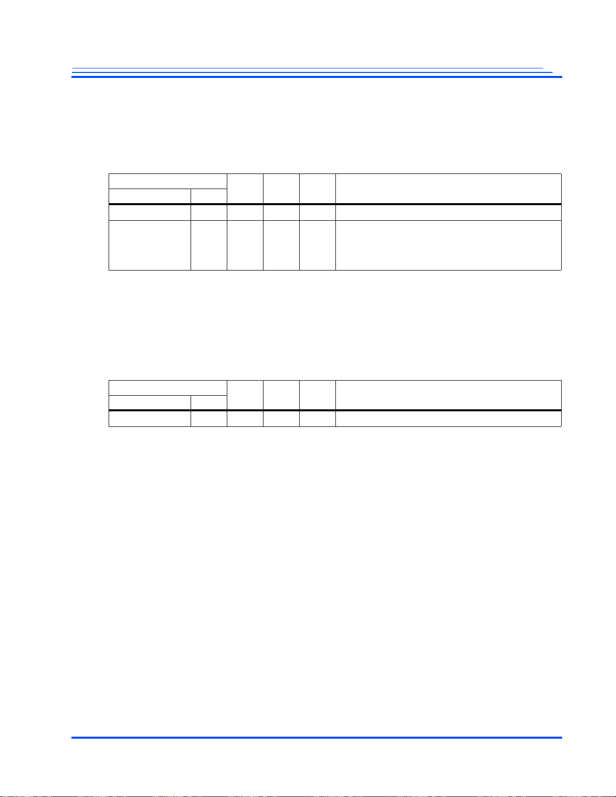
MG3500/MG2580 HD H.264 Codec SoC Data Sheet
2.3.17 Clock
The Clock Signal Group has two signals as shown in Table 2-20. These signals are all in the HOST
power domain. See “Clock and PLL inputs” on page 99.
Table 2-20 Clock Signals
Primary Signal
ALT GPIO Ball DescriptionName Type
CLK_IN I – – W15 Clock input
CLK_SEL I – – V14 Selects the source clock for the PLLs to come
2.3.18 Reset
from either the USB oscillator or CLK_IN.
0 = USB Oscillator
1 = External CLK_IN
The Reset Signal Group has one signal as shown in Table 2-21. This signal is in the AUD power domain.
Table 2-21 Reset Signals
Primary Signal
ALT GPIO Ball DescriptionName Type
RESETn I – – A22 Active Low chip reset
Maxim Integrated Products Advance Information | 51

MG3500/MG2580 HD H.264 Codec SoC Data Sheet
2.4 Power and Ground Pins
Table 2-22 Power Pins
Signal Name Ball Description Voltage
AUD_VDD F18 Power for the Audio Circuitry 1.8, 2.5, 3.3
AUD_VDD G17
AUD_GND E18 Ground for the Audio Circuitry –
AUD_GND F17
CORE_VDD E14 Power for the Core Logic 1.05 Volts
CORE_VDD F13
CORE_VDD F16
CORE_VDD H17
CORE_VDD J6
CORE_VDD R6
CORE_VDD U13
CORE_VDD U15
CORE_VDD V12
CORE_VDD V15
CORE_GND E17 Ground for the Core Logic –
CORE_GND G18
CORE_GND K6
CORE_GND L11
CORE_GND L12
CORE_GND M12
CORE_GND N12
CORE_GND N13
CORE_GND P6
CORE_GND V13
Volts
52 | Advance Information Maxim Integrated Products

MG3500/MG2580 HD H.264 Codec SoC Data Sheet
Table 2-22 Power Pins
Signal Name Ball Description Voltage
DDR_VDD H18 Power for the DDR Memory Controller 1.8 Volts
DDR_VDD J17
DDR_VDD K17
DDR_VDD L17
DDR_VDD N17
DDR_VDD P17
DDR_VDD R17
DDR_VDD R18
DDR_VDD T17
DDR_VDD U16
DDR_VDD U18
DDR_VDD V17
DDR_GND J18 Ground for the DDR Memory Controller –
DDR_GND K13
DDR_GND K18
DDR_GND L13
DDR_GND L18
DDR_GND M13
DDR_GND N18
DDR_GND P18
DDR_GND T18
DDR_GND U17
DDR_GND V16
DDR_GND V18
ETH_VDD G6 Power for the Ethernet circuitry 3.3 Volts
ETH_VDD H6
ETH_GND G5 Ground for the Ethernet circuitry –
ETH_GND H5
HOST_VDD T6 Power for the Host Processor 1.8, 2.5, 3.3
HOST_VDD U10
HOST_VDD U12
HOST_VDD U7
HOST_VDD U8
HOST_VDD U9
HOST_VDD N6
Volts
Maxim Integrated Products Advance Information | 53

MG3500/MG2580 HD H.264 Codec SoC Data Sheet
Table 2-22 Power Pins
Signal Name Ball Description Voltage
HOST_GND M6 Ground for the Host Processor –
HOST_GND M10
HOST_GND M11
HOST_GND N10
HOST_GND N11
HOST_GND U6
HOST_GND V5
PLL_VDD U14 Power for the Phase Lock Loop 1.05 Volts
USB_DVDD F11 Digital Power for the USB Port 1.05 Volts
USB_AVDD F10 Power for the USB Port 3.3 Volts
USB_AVDD F9 Power for the USB Port
USB_ACVDD F8 Power for the USB Port
USB_AGND E8 Analog Ground for the USB Port –
USB_AGND E9 Analog Ground for the USB Port
USB_AGND E10 Analog Ground for the USB Port
USB_ACGND E7 Analog Ground for the USB Port
USB_DGND K10 Digital Ground for the USB Port
VID01_VDD E15 Power for Video Ports 0 and 1 1.8, 2.5, 3.3
VID01_VDD F14
VID01_VDD F15
VID01_GND E16 Ground for Video Ports 0 and 1 –
VID01_GND K11
VID01_GND K12
VID23_VDD E6 Power for Video Ports 2 and 3 1.8, 2.5, 3.3
VID23_VDD F5
VID23_VDD F7
VID23_GND E5 Ground for Video Ports 2 and 3 –
VID23_GND F6
VID23_GND L10
Volts
Volts
54 | Advance Information Maxim Integrated Products

MG3500/MG2580 HD H.264 Codec SoC Data Sheet
2.5 Pin List by Power Group
Table 2-23 shows the signals associated with each of the power domains.
Table 2-23 Signal Group Names
Power
Domain
Voltage
Requirement
Group
Name Signals
HOST 1.8 , 2. 5, 3.3 HOST HOST_ A[6 :1], HOST_A[22:7], HOST_ALEn,
HOST_CS[5:0]n, HOST_D[15:0], HOST_D_EN,
HOST_DMARQ, HOST_INTn, HOST_REn, HOST_WAITn,
HOST_WEn, HOST_WP
CF CF_BVD1, CF_BVD2, CF_CD1, CF_CD2, CF_INPACKn,
CF_IORDn, CF_IOWRn, CF_REGn, CF_RESET,
CF_WAITn, CF_WP
SD SDMMC_CD, SDMMC_CLK, SDMMC_CMD, SDMMC_D3,
SDMMC_D2, SDMMC_D1, SDMMC_D0, SDMMC_WP
UART UARTD_RXD, UARTD_TXD, UART0_CTS, UART0_RTS,
UART0_RXD, UART0_TXD, UART1_RXD, UART1_TXD
SPI/BS SPI_MCLK, SPI_MISO, SPI_MOSI, SPI_MSS0, SPI_MSS1
TWI TWI0_SCL, TWI0_SDA
PWM PWM_0, PWM_1, PWM_2
GPIO GPIO_0_[0:7]
1
GPIO_1_00, GPIO_1_01, GPIO_1_02, GPIO_1_03,
GPIO_1_04, GPIO_1_05, GPIO_1_06, GPIO_1_07,
GPIO_1_08, GPIO_1_09, GPIO_1_10, GPIO_1_11,
GPIO_1_12, GPIO_1_13, GPIO_1_14, GPIO_1_15, GPIO_1_16, GPIO_1_17, GPIO_1_18,
GPIO_2_16, GPIO_2_17, GPIO_2_18, GPIO_2_19,
GPIO_2_20, GPIO_2_21, GPIO_2_22, GPIO_2_23,
GPIO_2_24, GPIO_2_25, GPIO_2_26, GPIO_2_27,
GPIO_2_28, GPIO_2_29, GPIO_2_30, GPIO_2_31
CLK CLK_IN, CLK_SEL
AUD 1.8, 2.5, 3.3 AUDx AUD0_BCK, AUD0_IDAT, AUD0_LRCK, AUD0_MCLK,
AUD0_ODAT0, AUD0_ODAT1, AUD0_ODAT2,
AUD0_SPDIF, AUD1_BCK, AUD1_IDAT, AUD1_LRCK,
AUD1_MCLK
RESET RESETn
JTAG JTAG_TAP_SEL, TEST, JTAG_TCK, JTAG_TDI,
JTAG_TDO, JTAG_TMS, JTAG_TRSTn
GPIO GPIO_1_20, GPIO_1_21, GPIO_1_22, GPIO_1_23,
GPIO_1_24
CORE 1.05 CORE No core signals are brought out directly to the I/O pins.
DDR 1.8 DDR DDR_PADHI, DDR_PADLO, DDR_A[12:0],
DDR_BA0, DDR_BA1, DDR_CASn, DDR_CKE,
DDR_CLK0, DDR_CLK0n, DDR_CLK1, DDR_CLK1n,
DDR_CSn, DDR_DQ[31:0],
DDR_DQM[3:0], DDR_DQS[3:0], DDR_DQS[3:0]n,
DDR_RASn, DDR_VREF, DDR_WEn
Maxim Integrated Products Advance Information | 55

MG3500/MG2580 HD H.264 Codec SoC Data Sheet
Table 2-23 Signal Group Names
Power
Domain
Voltage
Requirement
Group
Name Signals
ETH 3.3 ETH ETH_COL, ETH_CRS,
ETH_MDCLK, ETH_MDIO, ETH_RXCLK,
ETH_RXD[7:0], ETH_RXDV, ETH_RXER,
ETH_TXCLK, ETH_TXD[7:0], ETH_TXEN,
ETH_TXER
USB 3.3 USB USB_ANA_TST, USB_DM, USB_DP, USB_D_VBUS,
USB_ID, USB_REXT, USB_XIN, USB_XO
5.0 USB_VBUS
VID01 1.8 , 2. 5, 3. 3 VID01 , VIDx VID01_MCLK, VID01_MISO, VID01_MOSI, VID01_MSS
VID0_D[7:0], VID0_FIELD, VID0_HSYNC, VID0_OUTCLK,
VID0_PIXCLK, VID0_VSYNC,
VID1_D[7:0], VID1_FIELD, VID1_HSYNC, VID1_OUTCLK,
VID1_PIXCLK, VID1_VSYNC
CFG CFG_0, CFG_1, CFG_2, CFG_3, CFG_HOST0,
CFG_HOST1
GPIO GPIO_1_19, GPIO_1_25, GPIO_1_26, GPIO_1_27,
GPIO_1_28, GPIO_1_29, GPIO_1_30, GPIO_1_31;
GPIO_2_0, GPIO_2_1, GPIO_2_2, GPIO_2_3, GPIO_2_4,
GPIO_2_5
VID23 1.8 , 2. 5, 3. 3 VID23 , VIDx VID23_MCLK, VID23_MISO, VID23_MOSI, VID23_MSS,
VID2_D[7:0], VID2_FIELD, VID2_HSYNC, VID2_PIXCLK,
VID2_VSYNC,
VID3_D[7:0], VID23_D17, VID23_D16, VID3_GPIO
GPIO GPIO_2_6, GPIO_2_7, GPIO_2_8, GPIO_2_9, GPIO_2_10,
GPIO_2_11;
GPIO_2_12, GPIO_2_13, GPIO_2_14, GPIO_2_15
1. Only GPIO_0_[0:7] are the dedicated GPIOs; All other GPIO signals are multiplexed with other signals listed in Table 2-23.
For example, the primary function of GPIO_1_00 is a “host interrupt.” See Table 2-16 and Table 2-17 for detailed description.
56 | Advance Information Maxim Integrated Products

MG3500/MG2580 HD H.264 Codec SoC Data Sheet
2.6 Hookup Recommendations when Interfaces Are Unused
Table 2-24 shows the hookup recommendations when some of the interfaces are unused. The pull-up/
pull-down column indicates:
• UP: The pin has the internal pull-up enabled at power-on/reset.
• DOWN: The pin has the internal pull-down enabled at power-on/reset.
• DIS: The pin has pull-up/pull-down control, but they are disabled at power-on/reset.
• NONE: The pin has no control over pull-up/pull-down at all.
The Default column indicates the state the pin is in at reset:
• 0: The pin is driven to 0.
• 1: The pin is driven to 1.
• 0(p): The pin is pulled by a resistor to a 0 value.
• 1(p): The pin is pulled by resistor to a 1 value.
• Hi-Z: The pin is not driven.
• —: The pin is an Input Only, and must be driven.
• NC: The pin is a no connect (leave it unconnected).
Note: SDRAM and power pins are not included in this list since they must always be connected for the
device to operate correctly. This also applies when the USB block is not used on MG3500.
Internal pull-up and pull-down values are 15 KOhm ± 20%.
Table 2-24 Hookup Recommendations when Interfaces Are Unused
Pull-up/
Pin Name Dir Pad Type
VIDEO_PORT 0/1
VID01_MCLK O IO GPIO UP 0 NC
VID01_MISO I IO GPIO UP 1(p) NC, pulled up by default
VID01_MOSI O IO GPIO UP 1(p) NC, pulled up by default
VID01_MSS O IO GPIO UP 1 NC
VID0_D0 I I input_only NONE — GND
VID0_D1 I I input_only NONE — GND
VID0_D2 I I input_only NONE — GND
VID0_D3 I I input_only NONE — GND
VID0_D4 I I input_only NONE — GND
VID0_D5 I I input_only NONE — GND
Pull-down Default
Recommendation if the
Interface is Not Used
VID0_D6 I I input_only NONE — GND
VID0_D7 I I input_only NONE — GND
VID0_PIXCLK IO IO NONE Hi–Z GND
VID0_FIELD I IO GPIO UP 1(p) NC, pulled up by default
Maxim Integrated Products Advance Information | 57

MG3500/MG2580 HD H.264 Codec SoC Data Sheet
Table 2-24 Hookup Recommendations when Interfaces Are Unused
Pin Name Dir Pad Type
Pull-up/
Pull-down Default
Recommendation if the
Interface is Not Used
VID0_HSYNC I IO GPIO UP 1(p) NC, pulled up by default
VID0_VSYNC I IO GPIO UP 1(p) NC, pulled up by default
VID0_OUTCLK O O output_only NONE Hi–Z NC
VID1_D0 I I input_only NONE — GND
VID1_D1 I I input_only NONE — GND
VID1_D I I input_only NONE — GND
VID1_D3 I I input_only NONE — GND
VID1_D4 I I input_only NONE — GND
VID1_D5 I I input_only NONE — GND
VID1_D6 I I input_only NONE — GND
VID1_D7 I I input_only NONE — GND
VID1_PIXCLK IO IO NONE Hi–Z GND
VID1_FIELD I IO GPIO UP 1(p) NC, pulled up by default
VID1_HSYNC I IO GPIO UP 1(p) NC, pulled up by default
VID1_VSYNC I IO GPIO UP 1(p) NC, pulled up by default
VID1_OUTCLK O O output_only NONE Hi–Z NC
VIDEO_PORT 2/3
VID23_MCLK O IO GPIO UP 0 NC
VID23_MISO
VID23_MOSI
VID23_MSS
1
I IO GPIO UP 1(p) NC, pulled up by default
2
O IO GPIO UP 1(p) NC, pulled up by default
3
OIO GPIO UP 1 NC
VID2_D0 IO IO NONE Hi–Z NC, configure as output after reset
VID2_D1 IO IO NONE Hi–Z NC, configure as output after reset
VID2_D2 IO IO NONE Hi–Z NC, configure as output after reset
VID2_D3 IO IO NONE Hi–Z NC, configure as output after reset
VID2_D4 IO IO NONE Hi–Z NC, configure as output after reset
VID2_D5 IO IO NONE Hi–Z NC, configure as output after reset
VID2_D6 IO IO NONE Hi–Z NC, configure as output after reset
VID2_D7 IO IO NONE Hi–Z NC, Configure as output after reset
VID2_PIXCLK IO IO NONE Hi–Z NC, Configure as output after reset
VID2_FIELD IO IO GPIO UP 1(p) NC, pulled up by default
VID2_HSYNC IO IO GPIO UP 1(p) NC, pulled up by default
58 | Advance Information Maxim Integrated Products

MG3500/MG2580 HD H.264 Codec SoC Data Sheet
Table 2-24 Hookup Recommendations when Interfaces Are Unused
Pull-up/
Pin Name Dir Pad Type
VID2_VSYNC IO IO GPIO UP 1(p) NC, pulled up by default
VID3_D0 IO IO NONE Hi–Z NC, configure as output after reset
VID3_D1 IO IO NONE Hi–Z NC, configure as output after reset
VID3_D2 IO IO NONE Hi–Z NC, configure as output after reset
VID3_D3 IO IO NONE Hi–Z NC, configure as output after reset
VID3_D4 IO IO NONE Hi–Z NC, configure as output after reset
VID3_D5 IO IO NONE Hi–Z NC, configure as output after reset
VID3_D6 IO IO NONE Hi–Z NC, configure as output after reset
VID3_D7 IO IO NONE Hi–Z NC, configure as output after reset
VID23_D17 IO IO GPIO UP 1(p) NC, pulled up by default
VID23_D16 IO IO GPIO UP 1(p) NC, pulled up by default
VID23_GPIO IO IO GPIO UP 1(p) NC, pulled up by default
Pull-down Default
Recommendation if the
Interface is Not Used
Maxim Integrated Products Advance Information | 59

MG3500/MG2580 HD H.264 Codec SoC Data Sheet
Table 2-24 Hookup Recommendations when Interfaces Are Unused
Pin Name Dir Pad Type
4
USB
Pull-up/
Pull-down Default
Recommendation if the
Interface is Not Used
USB_D_VBUS A IO NC
USB_VBUS A IO NC
USB_DP A IO NC
USB_DM A IO NC
USB_ID A IO NC
USB_ANA_TST A IO NC
USB_REXT A IO USB_AVDD
USB_XIN A IO NC
USB_XO A IO NC
Ethernet
ETH_MDIO IO IO NONE Hi–Z 0 NC
ETH_MDCLK O IO NONE 0 1 NC
ETH_TXCLK I I NONE — — GND
ETH_TXD0 O IO NONE 0 1 NC
ETH_TXD1 O IO NONE 0 1 NC
ETH_TXD2 O IO NONE 0 1 NC
ETH_TXD3 O IO NONE 0 1 NC
ETH_TXD4 O IO NONE 0 1 NC
ETH_TXD5 O IO NONE 0 1 NC
ETH_TXD6 O IO NONE 0 1 NC
ETH_TXD7 O IO NONE 0 1 NC
ETH_TXEN O IO NONE 0 1 NC
ETH_TXER O IO NONE 0 1 NC
ETH_RXCLK I I NONE — — G ND
ETH_RXD0 I I NONE — — GND
ETH_RXD1 I I NONE — — GND
ETH_RXD2 I I NONE — — GND
ETH_RXD3 I I NONE — — GND
ETH_RXD4 I I NONE — — GND
ETH_RXD5 I I NONE — — GND
ETH_RXD6 I I NONE — — GND
60 | Advance Information Maxim Integrated Products

MG3500/MG2580 HD H.264 Codec SoC Data Sheet
Table 2-24 Hookup Recommendations when Interfaces Are Unused
Pin Name Dir Pad Type
Pull-up/
Pull-down Default
Recommendation if the
Interface is Not Used
ETH_RXD7 I I NONE — — GND
ETH_RXER I I NONE — — GND
ETH_RXDV I I NONE — — GND
ETH_COL I I NONE — — GND
ETH_CRS I I NONE — — GND
AUDIO
AUD0_BCK IO IO NONE Hi–Z N C, configure as output after reset
AUD0_IDAT I I GPIO
NONE Hi–Z GND
(input_only)
AUD0_LRCK IO IO NONE Hi–Z NC, configure as output after reset
AUD0_MCLK IO IO NONE Hi–Z NC, configure as output after reset
AUD0_ODAT0 O O output_only NONE 0 NC
AUD0_ODAT1 O O output_only NONE 0 NC
AUD0_ODAT2 O IO GPIO UP 0 NC
AUD0_SPDIF O IO GPIO UP 0 NC
AUD1_BCK IO IO GPIO UP 1(p) NC, pulled up by default
AUD1_IDAT I IO GPIO UP 1(p) NC, pulled up by default
AUD1_LRCK IO IO GPIO UP 1(p) NC, pulled up by default
AUD1_MCLK IO IO NONE Hi–Z NC, configure as output after reset
PWM
PWM_0 O IO GPIO UP 1 NC
PWM_1 O IO GPIO UP 1 NC
PWM_2 O IO GPIO UP 1 NC
SDMMC
SDMMC_CD I IO GPIO UP 1(p) NC, pulled up by default
SDMMC_CLK O O output_only NONE 0 NC
SDMMC_D0 O IO GPIO UP 1(p) NC, pulled up by default
SDMMC_D1 O IO GPIO UP 1(p) NC, pulled up by default
SDMMC_D2 O IO GPIO UP 1(p) NC, pulled up by default
SDMMC_D3 O IO GPIO UP 1(p) NC, pulled up by default
SDMMC_CMD IO IO GPIO UP 1(p) NC, pulled up by default
SDMMC_WP I IO GPIO UP 1(p) NC, pulled up by default
Maxim Integrated Products Advance Information | 61

MG3500/MG2580 HD H.264 Codec SoC Data Sheet
Table 2-24 Hookup Recommendations when Interfaces Are Unused
Pin Name Dir Pad Type
GPIO
Pull-up/
Pull-down Default
Recommendation if the
Interface is Not Used
GPIO_0 IO IO GPIO UP 1(p) NC
GPIO_1 IO IO GPIO UP 1(p) NC
GPIO_2 IO IO GPIO UP 1(p) NC
GPIO_3 IO IO GPIO UP 1(p) NC
GPIO_4 IO IO GPIO UP 1(p) NC
GPIO_5 IO IO GPIO UP 1(p) NC
GPIO_6 IO IO GPIO UP 1(p) NC
GPIO_7 IO IO GPIO UP 1(p) NC
TWI
TWI0_SCL IO IO GPIO UP 1(p) NC, pulled up by default
TWI0_SDA IO IO GPIO UP 1(p) NC, pulled up by default
SPI
SPI_MCLK IO IO GPIO UP 1(p) NC, pulled up by default
SPI_MISO IO IO GPIO UP 1(p) NC, pulled up by default
SPI_MOSI IO IO GPIO UP 1(p) NC, pulled up by default
SPI_MSS0 IO IO GPIO UP 1(p) NC, pulled up by default
SPI_MSS1 IO IO GPIO UP 1(p) NC, pulled up by default
UART
UARTD_RXD I I input_only NONE — Hook up to DBG_TXD
UARTD_TXD O O output_only NONE 1 Hook up to DBG_RXD
UART0_CTS I IO GPIO UP 1(p) NC, pulled up by default
UART0_RTS O IO GPIO UP 1 NC
UART0_RXD I IO GPIO UP 1(p) NC, pulled up by default
UART0_TXD O IO GPIO UP 1 NC
UART1_RXD I IO GPIO UP 1(p) NC, pulled up by default
UART1_TXD O IO GPIO UP 1 NC
62 | Advance Information Maxim Integrated Products

MG3500/MG2580 HD H.264 Codec SoC Data Sheet
Table 2-24 Hookup Recommendations when Interfaces Are Unused
Pin Name Dir Pad Type
HOST
Pull-up/
Pull-down Default
Recommendation if the
Interface is Not Used
HOST_A1 O IO NONE Hi–Z GND
HOST_A2 O IO NONE Hi–Z GND
HOST_A3 O IO NONE Hi–Z GND
HOST_A4 O IO NONE Hi–Z GND
HOST_A5 O IO NONE Hi–Z GND
HOST_A6 O IO NONE Hi–Z GND
HOST_A7 O O output_only NONE 0 NC
HOST_A8 O O output_only NONE 0 NC
HOST_A9 O O output_only NONE 0 NC
HOST_A10 O O output_only NONE 0 NC
HOST_A11 O O output_only NONE 0 NC
HOST_A12 O O output_only NONE 0 NC
HOST_A13 O O output_only NONE 0 NC
HOST_A14 O O output_only NONE 0 NC
HOST_A15 O O output_only NONE 0 NC
HOST_A16 O O output_only NONE 0 NC
HOST_A17 O O output_only NONE 0 NC
HOST_A18 O O output_only NONE 0 NC
HOST_A19 O O output_only NONE 0 NC
HOST_A20 O O output_only NONE 0 NC
HOST_A21 O O output_only NONE 0 NC
HOST_A22 O O output_only NONE 0 NC
HOST_ALEn O O output_only NONE 1 NC
HOST_CS_5n O O output_only NONE 1 NC
HOST_CS_4n O O output_only NONE 1 NC
HOST_CS_3n O O output_only NONE 1 NC
HOST_CS_2n O O output_only NONE 1 NC
HOST_CS_1n O IO NONE 1 NC
HOST_CS_0n O IO NONE 1 NC
HOST_D0 IO IO NONE Hi–Z GND
HOST_D1 IO IO NONE Hi–Z GND
Maxim Integrated Products Advance Information | 63

MG3500/MG2580 HD H.264 Codec SoC Data Sheet
Table 2-24 Hookup Recommendations when Interfaces Are Unused
Pull-up/
Pin Name Dir Pad Type
HOST_D2 IO IO NONE Hi–Z GND
HOST_D3 IO IO NONE Hi–Z GND
HOST_D4 IO IO NONE Hi–Z GND
HOST_D5 IO IO NONE Hi–Z GND
HOST_D6 IO IO NONE Hi–Z GND
HOST_D7 IO IO NONE Hi–Z GND
HOST_D8 IO IO NONE Hi–Z GND
HOST_D9 IO IO NONE Hi–Z GND
HOST_D10 IO IO NONE Hi–Z GND
HOST_D11 IO IO NONE Hi–Z GND
HOST_D12 IO IO NONE Hi–Z GND
HOST_D13 IO IO NONE Hi–Z GND
HOST_D14 IO IO NONE Hi–Z GND
HOST_D15 IO IO NONE Hi–Z GND
HOST_WPn O O output_only NONE 0 NC
Pull-down Default
Recommendation if the
Interface is Not Used
HOST_WAITn I IO NONE Hi–Z GND
HOST_INTn I IO UP 1(p) GND
HOST_REn O IO NONE 1 NC
HOST_WEn O IO NONE 1 NC
HOST_DMARQ I IO NONE 0 GND
HOST_D_EN O O output_only NONE 0 NC
CFG_HOST0 I I input_only NONE 0 GND
CFG_HOST1 I I input_only NONE 0 GND
CFG_0 I IO GPIO UP 1(p) NC, pulled up by default
CFG_1 I IO GPIO UP 1(p) NC, pulled up by default
CFG_2 I IO GPIO UP 1(p) NC, pulled up by default
CFG_3 I IO GPIO UP 1(p) NC, pulled up by default
64 | Advance Information Maxim Integrated Products
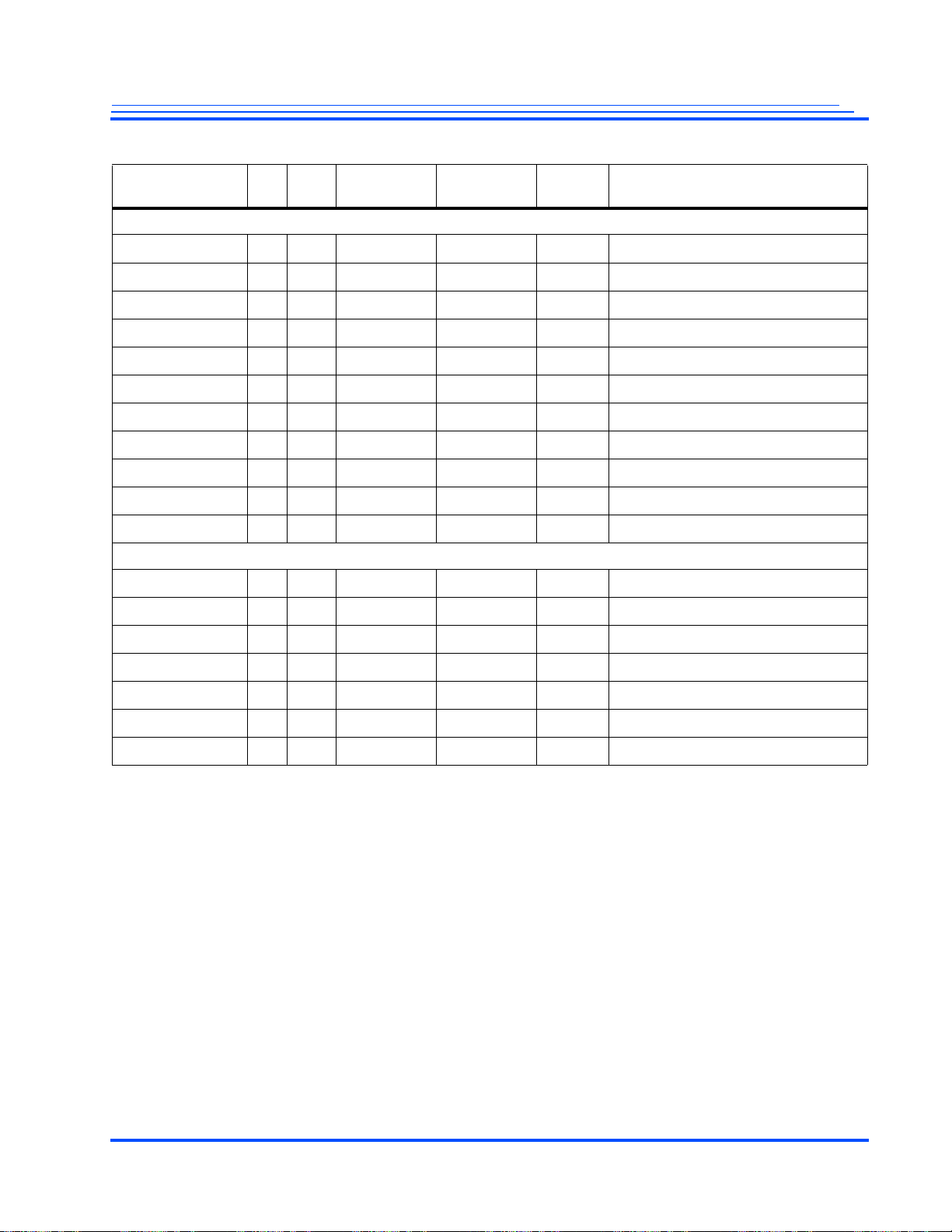
MG3500/MG2580 HD H.264 Codec SoC Data Sheet
Table 2-24 Hookup Recommendations when Interfaces Are Unused
Pin Name Dir Pad Type
CF
Pull-up/
Pull-down Default
Recommendation if the
Interface is Not Used
CF_WP I IO GPIO UP 1(p) NC, pulled up by default
CF_WAITn I IO GPIO UP 1(p) NC, pulled up by default
CF_IORDn O IO GPIO UP 1 NC
CF_IOWRn O IO GPIO UP 1 NC
CF_REGn O IO GPIO UP 1 NC
CF_RESET O IO GPIO UP 1 NC
CF_BVD1 I IO GPIO UP 1(p) NC, pulled up by default
CF_BVD2 I IO GPIO UP 1(p) NC, pulled up by default
CF_CD1 I IO GPIO UP 1(p) NC, pulled up by default
CF_CD2 I IO GPIO UP 1(p) NC, pulled up by default
CF_INPACKn I IO GPIO DOWN 0(p) NC, pulled down by default
JTAG
JTAG_TAP_SEL I I input_only NONE 1 GND
TEST I I input_only NONE 0 GND
JTAG_TCK I I input_only UP 1(p) GND
JTAG_TDI I I input_only UP 1(p) Hook up to TEST_TDO
JTAG_TDO O O output-only UP 1(p) Hook up to TEST_TDI
JTAG_TMS I I input_only UP 1(p) GND
JTAG_TRSTn I I input_only UP 1(p) GND
1. This pin does not apply to MG2580. See Table 2-4 for more information about MG2580 pin descriptions.
2. The same as above.
3. The same as above.
4. When the USB block is not used, in addition to connecting the USB pins as recommended in Table 2-24, the USB VDD pins still must
be connected to their standard supply levels, as shown below:
- USB_DVDD 1.05 V
- USB_AVDD 3.3 V
- USB_ACVDD 3.3 V
Maxim Integrated Products Advance Information | 65

MG3500/MG2580 HD H.264 Codec SoC Data Sheet
66 | Advance Information Maxim Integrated Products

3.0 Device Configuration
3.1 Reset
When the device is first powered on, the power supplies must be brought up in the order shown in
“Power Supply Sequencing” on page 193. Once the power supplies are stable follow this procedure to
reset the MG3500 SoC:
When the MG3500 SoC is being reset into Master (SOC) mode:
1. Set CLK_SEL pin to select the source clock for the PLLs. The clock can come from either the
internal USB oscillator or the CLK_IN pin.
2: Set the CFG_HOST[1:0] pins to 01 to select the Master configuration mode.
3: Set the boot mode using the CFG_[3-0] pins. See section 3.2 for more information.
4: Assert the RESETn pin low for at least one microsecond and then release it.
At this point, the ARM boot ROM will then start the initialization process.
When the MG3500 SoC is being reset into Slave (Coprocessor) mode:
MG3500/MG2580 HD H.264 Codec SoC Data Sheet
1. Set CLK_SEL pin to select the source clock for the PLLs. The clock can come from either the
internal USB oscillator or the CLK_IN pin.
2: Set the CFG_HOST[1:0] pins to either 00 to select Parallel Slave configuration mode or 11 to
select Serial Slave configuration mode.
3: Using the CFG_[3-0] pins, set the boot mode to 0xC (boot disabled).
4: Assert the RESETn pin low for at least one microsecond and then release it.
At this point, the Video Multi-Media Engine (MME) is ready to accept the firmware download.
Configure the Configuration/Status Registers, download the firmware, and start the other clocks. Then
wait for the MG3500 SoC to return a valid GPB (Global Pointer Block) before proceeding.
3.2 Boot modes for the MMEs and the ARM
At power up, an on-chip ROM that contains boot code starts executing. It will check for the clock source
(CLK_SEL), boot mode (CFG[0:3]) and continue on to start copying the bootloader from the specified
boot device.
Ensure that systems booting from NAND use the correct configuration. Each configuration will use
address cycles appropriate for the selected type of NAND.
Figure 3-1 lists the boot modes supported by the MG3500 in SoC mode.
Table 3-1 Boot Modes
CFG_3 CFG_2 CFG_1 CFG_0 Boot Mode
0000Load from large page 8-bit NAND <= 1 Gbits on CS1
0001Load from large page 8-bit NAND > 1 Gbits on CS1
0010Load from large page 16-bit NAND <= 1 Gbits on CS1
0011Load from large page 16-bit NAND > 1 Gbits on CS1
0100Load from small page 8-bit NAND <= 256 Mbits on CS1
1
1.
1.
Maxim Integrated Products Advance Information | 67
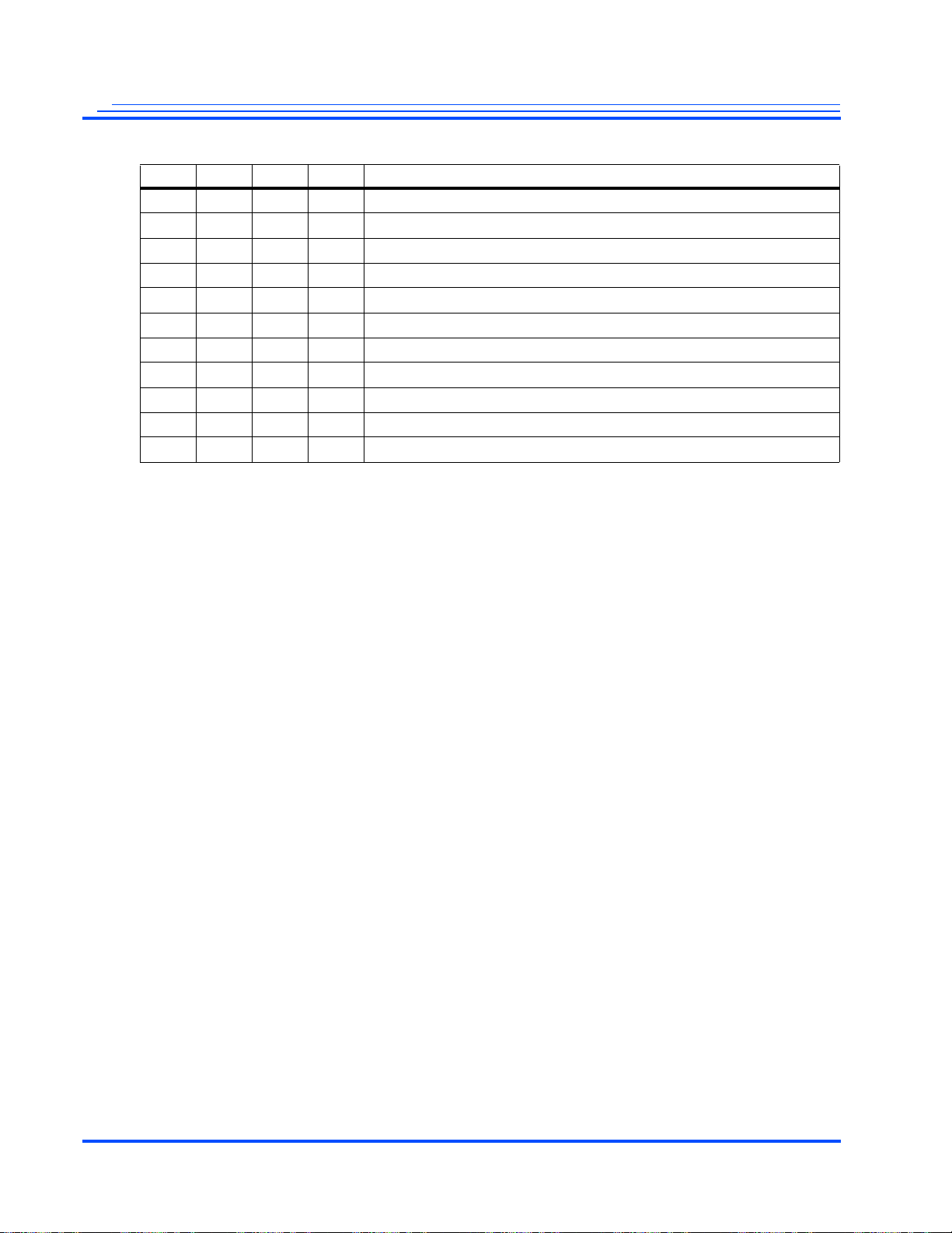
MG3500/MG2580 HD H.264 Codec SoC Data Sheet
Table 3-1 Boot Modes
CFG_3 CFG_2 CFG_1 CFG_0 Boot Mode
0101Load from small page 8-bit NAND > 256 Mbits on CS1
0110Reserved
0111Reserved
1000Reserved.
1001Load from SPI EEPROM (SPI 0).
1010Reserved.
1011Load from UARTDBG using Xmodem.
1100Boot disabled.
1101Boot from DDR.
1110Load from NOR Flash on CS0 using last 16 kBytes.
1111Reserved.
1. When 8-bit memories are specified, the data is taken from the upper 8-bits of the 16-bit data bus (HOST_D[15:8]).
1.
3.3 Firmware Loader
TBD: A description of the firmware loader and how it loads the operating software into the device.
3.4 API Configuration
The API that is supplied initializes the internal registers as part of the configuration process. These
registers include the:
• Configuration and Control registers
• Power control registers (core power, different I/O powers, etc.)
• Clock and PLL registers
The default configuration for the Clock and PLL registers assumes that you are using the 12 MHz USB
crystal as the primary clock source. It is also possible to drive the device using an externally generated
24 or 27 MHz clock. If you plan on using one of these external clocks, contact Mobilygen Technical
Support for a specialized version of the API.
3.5 Pin Multiplexing, GPIOs, etc.
All shared I/O pins come up in the primary interface mode, and must be programmed to be used in the
Alternate interface mode or GPIO mode. Dedicated GPIO pins come up as input pins, and must be
programmed in order to be used as output pins.
3.6 Debug Mode
The API supports communication between the ARM processor and the Debug port. Any messages seen
on the Debug port come from the firmware. The Debug port is very useful in debugging the system and
should always be connected.
3.7 JTAG ID Register
This section provides a description and listing of the JTAG ID Register.
68 | Advance Information Maxim Integrated Products

MG3500/MG2580 HD H.264 Codec SoC Data Sheet
31 30 29 28 27 26 25 24 23 22 21 20 19 18 17 16
Version Manufacturers Part Number[15:4]
1514131211109 876543210
Part Number[3:0] Manufactu re rs ID 1
Reserved fields should be ignored (masked) when read, and only 0's should be written to them.
Version 4-bit Version code of the device. Currently set to 0x0.
Part Number 16-bit Manufacturers Part Number, assigned by Mobilygen. Currently set to 0x0300.
Manufacturers ID 11-bit Manufacturers identity code (Mobilygen specific), assigned by JTAG. This is set
1 This bit is always set to 1.
to 0x2EB.
Maxim Integrated Products Advance Information | 69

MG3500/MG2580 HD H.264 Codec SoC Data Sheet
70 | Advance Information Maxim Integrated Products

4.0 Device Operating Conditions
4.1 Absolute Maximum Ratings
T able 4-1 gives the absolute maximum ratings. Exposure to stresses beyond those listed in this table can
result in device unreliability, permanent damage, or both.
Table 4-1 Absolute Maximum Ratings
Parameter Value Units Notes
CORE_VDD 1.5 V —
DDR_VDD 2.5 V —
VID01_VDD 4.5 V —
VID23_VDD 4.5 V —
AUD_VDD 4.5 V —
HOST_VDD 4.5 V —
USB_VDD 4.5 V —
ETH_VDD 4.5 V —
Maximum Input Voltage, DDR 2.1 V DDR_VDD + 300 mV
Maximum Input Voltage, Other I/O VDD_VREF +
Storage Temperature Range -40 to 150 °C —
MG3500/MG2580 HD H.264 Codec SoC Data Sheet
V Referenced to associated IO VDD
700 mV
4.2 Recommended Operation Conditions
Table 4-2 specifies the operating conditions.
Table 4-2 Operating Conditions
Parameter Minimum Typical Maximum Units Notes
CORE_VDD
PLL_VDD
VID01_VDD
VID23_VDD
AUD_VDD
HOST_VDD
USB_VDD 2.97 3.3 3.63 V 3.3V ±10%
ETH_VDD 3.13 3.3 3.46 V 3.3V ±5%
DDR_VDD 1.7 1.8 1.9 V 1.8V ±0.1V
DDR_VREF - 0.60 x
Operating Temperature
Range (case)
0.9975 1.05 1.1025 V 1.05V ± 5%
1.62
2.25
2.97
05090°C—
1.8
2.5
3.3
DDR_VDD
1.98
2.75
3.63
- V This should be tuned for ev-
V Programmable Voltage
1.8 / 2.5 / 3.3V ±10%
ery design.
Refer to DDR design guide-
line, "MG3500/MG2580
DDR2 User's Guide.”
Use 1% resistors
Maxim Integrated Products Advance Information | 71

MG3500/MG2580 HD H.264 Codec SoC Data Sheet
4.3 Essential Characteristics
Table 4-3 defines the DC characteristics for all of the interfaces except the SDRAM interface.
Table 4-3 DC Characteristics
VID01_VDD,
VID23_VDD,
AUD_VDD,
HOST_VDD
3.3V ±10%
Symbol Parameters Test Conditions
VIH Input High Level VDD = Maximum 2.00 —
V
IL
V
OH
V
OL
I
IH
I
IL
C
PIN
1. The I/O pads are optimized for 3.3 Volt operation. The outputs should scale proportionately for 2.5 and 1.8 Volt operation, but the actual
values may vary, depending on the individual device.
2. Not 100% tested.
Input Low-Level
VDD = Minimum — 0.40 V
Voltage
Output High-Level
Voltage
Output Low-Level
Voltage
VDD = Minimum,
= –4 mA
I
OH
VDD = Minimum,
= –4 mA
I
OL
Input Leakage VDD = Maximum,
= V
V
IN
DD
Input Leakage VDD = Maximum,
= 0V
V
IN
——5 pF
Capacitance
2
2.70 — V
—0.42 V
–5 –5 µA
–2.55 –2.55 µA
VID01_VDD,
VID23_VDD,
AUD_VDD,
HOST_VDD
2.5V ±10%
VID01_VDD,
VID23_VDD,
AUD_VDD,
HOST_VDD
1
1.8 V ±10%
See Note 1 See Note 1
1
UnitsMin Max Min Max Min Max
V
Table 4-3 defines the DC and AC characteristics for the DDR SDRAM interface.
Table 4-4 DC Characteristics
Symbol Parameters Test Conditions
V
DCIH
V
DCIL
V
ACIH
V
ACIL
V
DCOH
V
DCOL
V
ACOH
V
ACOL
C
PIN
1. Not 100% tested.
Input DC High Level VDD = Maximum DDR_VREF + 125 mV DDR_VDD + 300 mV V
Input DC Low-Level VDD = Minimum 0 DDR_VREF – 125 mV V
Input AC High Level VDD = Maximum DDR_VREF + 250 mV DDR_VDD + 300 mV V
Input AC Low-Level VDD = Minimum 0 DDR_VREF – 250 mV V
Output DC High Level VDD = Maximum 1.4 DDR_VDD V
Output DC Low-Level VDD = Minimum 0 DDR_VREF – 250 mV V
Output AC High Level VDD = Maximum 1.3 DDR_VDD V
Output AC Low-Level VDD = Minimum 0 0.5 V
Capacitance
1
—— 5pF
DDR_VDD
1.8 V ±10%
UnitsMin Max
72 | Advance Information Maxim Integrated Products

MG3500/MG2580 HD H.264 Codec SoC Data Sheet
4.4 Power Supply Currents for the Different Power Domains
The power supply input currents vary for each power domain. Table 4-5 shows the input current ranges
for each of the domains.
Table 4-5 Typical Power Supply Currents for the Different Power Domains
Domain Conditions Minimum Typical Maximum Units
CORE 1.0 Volt Supply Voltage 1000 mA
AUD 3.3 Volt Supply Voltage 18 mA
ETH 3.3 Volt Supply Voltage 42 mA
HOST 3.3 Volt Supply Voltage 42 mA
DDR 1.8 Volt Supply Voltage 166 mA
USB 3.3 Volt Supply Voltage 18 mA
VID01 3.3 Volt Supply Voltage 45 mA
VID23 3.3 Volt Supply Voltage 45 mA
4.5 AC Timing
This section provides the AC timing for the MG3500 SoC’s various interfaces. This section is divided
into the following subsections:
• “MG3500 Parallel Slave Host Interface Timing” on page 74
• “Video Interface AC Timing” on page 78
• “Audio Interface AC Timing” on page 81
• “SDRAM Interface AC Timing” on page 88
Maxim Integrated Products Advance Information | 73

MG3500/MG2580 HD H.264 Codec SoC Data Sheet
HOST_CS0
HOST_A[6:1]
HOST_D[15:0]
H
OST_WE
HOST_RE
HOST_DMARQ
Address Address
Write Data Read Data
t
WAS
t
WDC
t
WAH
t
WDH
t
RAS
t
RAH
t
RDD
t
WEC
t
CWE
t
WEA
t
CSH
t
RDV
t
RDH
Max 4 CLK + t
RQD
HOST_DMARQ takes three to four core clock (clk) periods before becoming valid
t
CSA
4.5.1 MG3500 Parallel Slave Host Interface Timing
Figure 4-1 shows the timing diagram for the MG3500 Parallel Slave Host Interface, Figure 4-2 shows
the DMA Timing, Figure 4-3 shows the W ait timing, and Figure 4-4 shows the Interrupt Request timing.
Table 4-6 lists the timing parameters for each of these diagrams.
Figure 4-1 Parallel Slave Host Slave Interface AC Timing Waveform
74 | Advance Information Maxim Integrated Products
Figure 4-2 HOST_DMARQ Timing
CLK
HOST_WE
HOST_RE
HOST_DMARQ
t
CLK
t
CLK
represents SDRAM clock cycles, not XIN cycles
HOST_DMARQ
takes three to four core clock (clk) periods before becoming valid
t
RQD
CLK
HOST_WE
HOST_RE
HOST_WAIT
HOST_WE
HOST_RE
HOST_WAIT
The Host Interface needs three to four
core clock (clk) cycles at the end of a
host access before HOST_WAIT
is
valid.
t
WD
t
CLK
t
WV
Short Time Between Accesses <2 Core Clock Periods
t
WD
t
WV
Long Time Between Accesse s >2 Core Clock Periods
The Host Interface generates
HOST_WAIT
from the core clock so
the leading edge of HOST_RE
or
HOST_WE
, HOST_WAIT may not be
valid for one core clock (clk) cycle, plus
some combinatorial delay.
t
CLK
represents internal core clock (clk) cycles, not XIN cycles
MG3500/MG2580 HD H.264 Codec SoC Data Sheet
Figure 4-3 HOST_WAIT
Timing
Maxim Integrated Products Advance Information | 75

MG3500/MG2580 HD H.264 Codec SoC Data Sheet
CLK
HOST_INT
t
CLK
t
ID
t
CLK
represents internal core clock (clk) cycles, not XIN cycles
Figure 4-4 HOST_INT Timing
76 | Advance Information Maxim Integrated Products

MG3500/MG2580 HD H.264 Codec SoC Data Sheet
Table 4-6 Slave Host Interface Timing
Signal Parameter Description Min
Core Clock t
HOST_A[6:1] t
HOST_D[15:0] t
HOST_WE t
HOST_RE t
HOST_CS t
HOST_DMARQ t
HOST_IRQ T
HOST_WAIT t
1. These numbers are based on simulation and will probably improve after characterization of the actual part.
CLK
WAS
t
WAH
t
RAS
t
RAH
t
CSA
WDC
t
WDH
t
RDD
t
RDV
t
RDH
CWE
t
WEC
t
WEA
CRE
t
REC
t
REA
CSH
RQD
WD
t
WV
ID
XIN x PLL Frequency — 180 MHz
HOST_A[6:1] setup to trailing edge
OST_WE for write cycles
H
HOST_A[6:1] hold from trailing edge
OST_WE for write cycles
H
HOST_A[6:1] setup to leading edge
OST_RE for read cycles
H
HOST_A[6:1] hold from trailing edge
OST_RE for read cycles
H
HOST_A[6:1] setup to leading edge of
OST_CS
H
HOST_D[15:0] setup to trailing edge
OST_WE for write cycles
H
HOST_D[15:0] hold from trailing edge
OST_WE for write cycles
H
HOST_D[15:0] driven from leading edge
OST_RE for read cycles
H
HOST_D[15:0] valid from leading edge
OST_RE for read cycles
H
HOST_D[15:0] hold from trailing edge
OST_RE for read cycles
H
HOST_CS Active to HOST_WE Active 0 — ns
HOST_WE Inactive to HOST_CS Inactive 3 — ns
HOST_WE active time 20 — ns
HOST_CS Active to HOST_RE Active 0 — ns
HOST_RE Inactive to HOST_CS Inactive 0 — ns
HOST_RE active time 20 — ns
HOST_CS inactive time between
accesses
HOST_DMARQ valid from internal clock — 8 ns
HOST_IRQ valid from internal clock — 8 ns
HOST_WAIT valid from internal clock — 8 ns
HOST_WAIT valid from HOST_RE/
OST_WE
H
1
20 — ns
3 — ns
0 — ns
0 — ns
0 — ns
12 — ns
3 — ns
0 — ns
— 17 ns
2 11 ns
10 — ns
— 12 ns
Max
1
Units
Maxim Integrated Products Advance Information | 77

MG3500/MG2580 HD H.264 Codec SoC Data Sheet
VID_CLK
VID_DATA
VIDOUT_DATA
HSYNC,
VSYNC,
FIELD
t
VF
t
VIS
t
VIH
t
VC
t
VCQ
t
VL
t
VH
t
VR
t
VIS
4.5.2 Video Interface AC Timing
Figure 4-5 and Table 4-7 show the AC timing parameters for the video interface.
Table 4-7 Standard Definition Video Interface AC Timing Values
1. All timing values are in respect to rising edge on the VID_CLK pin. This clock can be supplied by either the external device or by the
Figure 4-5 Video Interface Timing Diagram
Signal Parameter Description
VID[0:2]_CLK
VID[0:1]_DATA,
HSYNC[0:1],
VSYNC[0:1],
FIELD[0:1]
VID[2:3]_DATA,
HSYNC[2:3],
VSYNC[2:3],
FIELD[2:3]
VIDOUT[0:1] _DATA,
HSYNC[0:1],
VSYNC[0:1],
FIELD[0:1
VIDOUT[2:3] _DATA,
HSYNC[2:3],
VSYNC[2:3],
FIELD[2:3]
MG3500 SoC.
t
t
t
t
t
t
VIS
t
VIH
t
VIS
t
VIH
t
VCQ
t
VCQ
VC
VH
VL
VR
VF
Timing Value (ns.)
1
VID_CLK Cycle Time (27 MHz) — 37.037 ns
VID_CLK High Time 16.67 18.5 20.37 ns
VID_CLK Low Time t
VC - tVH
VID_CLK Slew (Rise Time) Not Applicable
VID_CLK Slew (Fall Time) Not Applicable
VID_DATA, HSYNC, VSYNC, FIELD Set-
3.5 — — ns
up Time to VID0_CLK or VID1_CLK
VID_DATA, HSYNC, VSYNC, FIELD
2.8 — — ns
Hold Time from VID0_CLK or VID1_CLK
VID_DATA, HSYNC, VSYNC, FIELD Set-
3.5 — — ns
up Time to VID2_CLK
VID_DATA, HSYNC, VSYNC, FIELD
Hold Time from VID2_CLK
VIDOUT_DATA, HSYNC, VSYNC,
2.8 — — ns
4.0 — 13 ns
FIELD Delay from VID0_CLK or
VID1_CLK
VIDOUT_DATA, HSYNC, VSYNC,
4.0 — 13 ns
FIELD Delay from VID2_CLK
UnitsMin Typ Max
78 | Advance Information Maxim Integrated Products

MG3500/MG2580 HD H.264 Codec SoC Data Sheet
Table 4-8 High Definition Video Interface AC Timing Values
1
UnitsMin Typ Max
Signal Parameter Description
VID[0:2]_CLK
2
VID[0:1]_DATA
,
HSYNC[0:1],
VSYNC[0:1],
FIELD[0:1]
2
VID[2:3]_DATA
,
HSYNC[2:3],
VSYNC[2:3],
FIELD[2:3]
VIDOUT[0:1]_DATA,
HSYNC[0:1],
t
t
t
t
t
t
VIS
t
VIH
t
VIS
t
VIH
t
VCQ
VC
VH
VL
VR
VF
Timing Value (ns.)
VID_CLK Cycle Time (74.25 MHz) — 13.468 ns
VID_CLK High Time 6.06 6.73 7.41 ns
VID_CLK Low Time t
VC - tVH
VID_CLK Slew (Rise Time) Not Applicable
VID_CLK Slew (Fall Time) Not Applicable
VID_DATA, HSYNC, VSYNC, FIELD Set-
2.5 — — ns
up Time to VID0_CLK or VID1_CLK
VID_DATA, HSYNC, VSYNC, FIELD Hold
2.8 — — ns
Time from VID0_CLK or VID1_CLK
VID_DATA, HSYNC, VSYNC, FIELD Set-
2.5 — — ns
up Time to VID2_CLK
VID_DATA, HSYNC, VSYNC, FIELD Hold
2.8 — — ns
Time from VID2_CLK
VIDOUT_DATA, HSYNC, VSYNC, FIELD
4.0 — 11.3 ns
Delay from VID0_CLK or VID1_CLK
VSYNC[0:1],
FIELD[0:1]
VIDOUT[2:3]_DATA,
HSYNC[2:3],
t
VCQ
VIDOUT_DATA, HSYNC, VSYNC, FIELD
Delay from VID2_CLK
4.0 — 11.3 ns
VSYNC[2:3],
FIELD[2:3]
1. All timing values are in respect to rising edge on the VID_CLK pin. This clock should be supplied either by the external device or by the
the MG3500 SoC.
2. The external device should drive the data on the falling edge of VID_CLK to satisfy the input hold requirements.
Maxim Integrated Products Advance Information | 79

MG3500/MG2580 HD H.264 Codec SoC Data Sheet
Table 4-9 High-Speed Video Interface AC Timing Values
Timing Value (ns.)
Signal Parameter Description
VID[0:2]_CLK
VID[0:1]_DATA
2
,
HSYNC[0:1],
VSYNC[0:1],
FIELD[0:1]
VID[2:3]_DATA
2,
HSYNC[2:3],
VSYNC[2:3],
FIELD[2:3]
VIDOUT[0:1]_DATA
HSYNC[0:1],
t
VC
t
VH
t
VL
t
VR
t
VF
t
VIS
t
VIH
t
VIS
t
VIH
t
VCQ
VID_CLK Cycle Time (125 MHz) — 8.0 ns
VID_CLK High Time 3.6 4 4.4 ns
VID_CLK Low Time t
VC - tVH
VID_CLK Slew (Rise Time) Not Applicable
VID_CLK Slew (Fall Time) Not Applicable
VID_DATA, HSYNC, VSYNC, FIELD Set-
1.8 — — ns
up Time to VID0_CLK or VID1_CLK
VID_DATA, HSYNC, VSYNC, FIELD Hold
2.8 — — ns
Time from VID0_CLK or VID1_CLK
VID_DATA, HSYNC, VSYNC, FIELD Set-
1.8 — — ns
up Time to VID2_CLK
VID_DATA, HSYNC, VSYNC, FIELD Hold
2.8 — — ns
Time from VID2_CLK
VIDOUT_DATA, HSYNC, VSYNC, FIELD
1.8 — 6 ns
Delay from VID0_CLK or VID1_CLK
VSYNC[0:1],
FIELD[0:1]
VIDOUT[2:3]_DATA
HSYNC[2:3],
t
VCQ
VIDOUT_DATA, HSYNC, VSYNC, FIELD
Delay from VID2_CLK
1.8 — 6 ns
VSYNC[2:3],
FIELD[2:3]
1. All timing values are in respect to rising edge on the VID_CLK pin. This clock can be supplied by the MG3500 SoC.
2. The external device should drive the data on the falling edge of VID_CLK to satisfy the input hold requirements.
3. High-speed video interface is used when the video inputs are multiplexed.
1
UnitsMin Typ Max
80 | Advance Information Maxim Integrated Products

MG3500/MG2580 HD H.264 Codec SoC Data Sheet
AUDx_MCLK
AUD_LRCK
AUD_BCK
256 AUDx_MCLKs
64/32 AUD_BCKs
AUD_IDAT
AUD_ODAT
AUD_BCK
AUD_LRCK
16-Bit
20-Bit
24-Bit
MSB
Word n
Right Channel
Word n
Left Channel
n
n+1
n+15
LSB MSB
n n+1 n+19
n
n+1
n+23
n+15
n+31
or
n+31
n+31
4.5.3 Audio Interface AC Timing
This section gives the AC timing parameters for the audio interface. Figure 4-6 shows the relationships
between the three audio clocks. Figure 4-8 shows the left-justified audio timing waveforms.
Table 4-10
lists the AC timing for Audio Operations.
Figure 4-6 Standard Audio Timing Diagram
Figure 4-6 shows the I2S protocol, where the MSB bit is sent one AUD_BCK cycle after the
AUD_LRCK signal has transitioned. In this mode, when LRCK is high the data is from the right
channel, and when LRCK is low the data is from the left channel. This is opposite of left-justified audio.
Figure 4-7 shows sample waveforms for 16-, 20-, and 24-bit Left Justified audio. LRCK needs to be 64
BCKs in 20- and 24-bit modes. The MSB for each audio sample is aligned with LRCK's transition. The
Audio Input Interface ignores the data bus after the LSB for each sample.
Figure 4-7 16, 20, and 24-Bit Left Justified Audio Waveform
Maxim Integrated Products Advance Information | 81

MG3500/MG2580 HD H.264 Codec SoC Data Sheet
AUD_BCK
AUD_LRCK
AUD_IDAT
AUD_ODAT
t
BF
t
DVW
t
BC
t
BL
t
BH
t
BR
t
DVW
Figure 4-8 Audio Interface Timing Diagram
Table 4-10 Audio Interface AC Timing Values
Timing Value (ns.)
Signal Parameter Description
t
t
t
BC
BC
BC
AUD_BCK Cycle Time
(Fs = 48 kHz, 64 BCK/Sample)
AUD_BCK Cycle Time
(Fs = 48 kHz, 32 BCK/Sample)
AUD_BCK Cycle Time
—325.5— ns
— 651.04 — ns
— 488.28 — ns
UnitsMin Typ Max
(Fs = 32 kHz, 64 BCK/Sample)
AUD_BCK
t
BC
AUD_BCK Cycle Time
— 976.56 — ns
(Fs = 32 kHz, 32 BCK/Sample)
AUD_LRCK
AUD_ODAT
AUD_IDAT
t
t
t
t
t
DVW
t
DVW
BH
BL
BR
BF
AUD_BCK High Time tBC/2 * 0.8 tBC/2 tBC/2 * 1.2 ns
AUD_BCK Low Time (tBC - tBH)t
BC
– t
BH
AUD_BCK Slew (Rise Time) — — 3 ns
AUD_BCK Slew (Fall Time) — — 3 ns
1
Data Valid Window for Slave
tBC/4 + 15 — — ns
Mode operation
(Fs = 48 kHz or 32 kHz)
Data Valid Window for Master
tBC/4 – 15 — — ns
Mode operation
ns
(Fs = 48 kHz or 32 kHz)
1. There is no restriction on the position of the Data Valid Window relative to BCK. The internal data sampling position is programmable
and can be repositioned in t
/4 steps.
BC
82 | Advance Information Maxim Integrated Products

MG3500/MG2580 HD H.264 Codec SoC Data Sheet
ETH_TXCLK
ETH_TXEN
ETH_TXER
ETH_TXD[7:0]
t
XCCKO
t
ETCYC
t
ETL
t
ETH
t
XDCKO
4.5.4 Ethernet Interface AC Timing
This section shows the AC timing parameters for the Ethernet interface in each of the three operating
modes:
•GMII
•MII
•RMII
Refer to the individual section for specific information.
Gigabit Media Independent Interface (GMII) AC Timing
The Gigabit Media Independent Interface (GMII) defines speeds up to 1000 Mbit/s, implemented using
an 8-bit data interface clocked at 125 MHz.
Figure 4-9 shows the AC timing parameters for the Ethernet interface in GMII Transmit mode, and
Figure 4-10 shows the AC timing parameters for the Ethernet interface in GMII Receive mode.
Figure 4-9 Ethernet Interface GMII Transmit Timing Diagram
Table 4-11 Ethernet GMII Transmit Interface AC Timing Values
Timing Value (ns.)
Signal Parameter Description
t
ECYC
t
ETH_TXCLK
ETH_TXEN
ETH_TXER
ETH_TXD[7:0]
1. The minimum clock low and high times specify a worst case 60/40 duty cycle.
ETL
t
ETH
t
XCCKO
t
XDCKO
Ethernet GMII Transmit Clock Cycle
Time
Ethernet GMII Transmit Clock Low
1
Time
Ethernet GMII Transmit Clock Low
1
Time
Ethernet GMII Transmit Control Sig-
nal Clock to Output Time
Ethernet GMII Transmit Data
Clock to Output Time
—8.0— ns
3.2 — — ns
3.2 — — ns
2.0 — 5.9 ns
2.0 — 5.9 ns
UnitsMin Typ Max
Maxim Integrated Products Advance Information | 83

MG3500/MG2580 HD H.264 Codec SoC Data Sheet
t
RDS
ETH_RXCLK
ETH_RXDV
ETH_RXER
ETH_RXD[7:0]
t
RCH
t
ECYC
t
EL
t
EH
t
RDH
t
RCS
Figure 4-10 Ethernet Interface GMII Receive Timing Diagram
Table 4-12 Ethernet GMII Receive Interface AC Timing Values
Signal Parameter Description
t
ECYC
t
ETH_RXCLK
ETL
t
ETH
t
RCS
ETH_RXDV
ETH_RXER
t
RCH
t
RDS
ETH_RXD[7:0]
t
RDH
1. The minimum clock low and high times specify a worst case 60/40 duty cycle.
Ethernet GMII Receive Clock Cycle
Time
Ethernet GMII Receive Clock Low
1
Time
Ethernet GMII Receive Clock High
1
Time
Ethernet GMII Receive Control Sig-
nal Setup Time
Ethernet GMII Receive Control Sig-
nal Hold Time
Ethernet GMII Receive Data Setup
Time
Ethernet GMII Receive Data Hold
Time
Timing Value (ns.)
UnitsMin Typ Max
—8.0—ns
3.2 — 4.8 ns
3.2 — 4.8 ns
2.2 — — ns
0——ns
2.2 — — ns
0——ns
84 | Advance Information Maxim Integrated Products

MG3500/MG2580 HD H.264 Codec SoC Data Sheet
ETH_TXCLK
ETH_TXEN
ETH_TXER
ETH_TXD[3:0]
t
XCCKO
t
ECYC
t
ETL
t
ETH
t
XDCKO
Media Independent Interface (MII) AC Timing
The Media Independent Interface (MII) defines speeds up to 100 Mbit/s, implemented using an 4-bit
data interface clocked at either 25 MHz or 2.5 MHz.
Figure 4-11 shows the AC timing parameters for the Ethernet interface in MII Transmit mode, and
Figure 4-12 shows the AC timing parameters for the Ethernet interface in MII Receive mode.
Figure 4-11 Ethernet Interface MII Transmit Timing Diagram
Table 4-13 Ethernet MII Transmit Interface AC Timing Values
Signal Parameter Description
t
ECYC
t
ETH_TXCLK
ETH_TXEN
ETH_TXER
ETH_TXD[3:0]
1. The minimum clock low and high times specify a worst case 60/40 duty cycle.
ETL
t
ETH
t
XCCKO
t
XDCKO
Ethernet MII Transmit Clock Cycle
Time
Ethernet MII Transmit Clock Low
1
Time
Ethernet MII Transmit Clock High
1
Time
Ethernet MII Transmit Control Signal
Clock to Output Time
Ethernet MII Transmit Data
Clock to Output Time
Timing Value (ns.)
UnitsMin Typ Max
— 40.0 — ns
16.0 — 24.0 ns
16.0 — 24.0 ns
2.0 — 5.9 ns
2.0 — 5.9 ns
Maxim Integrated Products Advance Information | 85

MG3500/MG2580 HD H.264 Codec SoC Data Sheet
t
RDS
ETH_RXCLK
ETH_RXDV
ETH_RXER
ETH_RXD[3:0]
t
ECYC
t
EL
t
EH
t
RDH
t
RCH
t
RCS
Figure 4-12 Ethernet Interface MII Receive Timing Diagram
Table 4-14 Ethernet MII Receive Interface AC Timing Values
Signal Parameter Description
t
ECYC
t
ETH_RXCLK
ETL
t
ETH
t
RCS
ETH_RXDV
ETH_RXER
t
RCH
t
RDS
ETH_RXD[3:0]
t
RDH
1. The minimum clock low and high times specify a worst case 60/40 duty cycle.
Ethernet MII Receive Clock Cycle
Time
Ethernet MII Receive Clock Low
1
Time
Ethernet MII Receive Clock High
1
Time
Ethernet MII Receive Control Signal
Setup Time
Ethernet MII Receive Control Signal
Hold Time
Ethernet MII Receive Data Setup
Time
Ethernet MII Receive Data Hold Time 0 — — ns
Timing Value (ns.)
UnitsMin Typ Max
— 40.0 — ns
16.0 — 24.0 ns
16.0 — 24.0 ns
2.2 — — ns
0——ns
2.2 — — ns
86 | Advance Information Maxim Integrated Products

MG3500/MG2580 HD H.264 Codec SoC Data Sheet
ETH_RXCLK
ETH_TXEN
ETH_TXD[1:0]
t
XCCKO
t
ECYC
t
ETL
t
ETH
t
XDCKO
Reduced Media Independent Interface (RMII) AC Timing
The Reduced Media Independent Interface (RMII) defines speeds up to 100 Mbit/s, implemented using
a 2-bit data interface clocked at 50 MHz. For transmit data, the RMII interface only uses the
ETH_TXEN and ETH_TXD[1:0] pins. For receive data, the RMII interface only uses the ETH_RXDV
and ETH_RXD[1:0] pins.
Figure 4-13 shows the AC timing parameters for the Ethernet interface in RMII Transmit mode, and
Figure 4-14 shows the AC timing parameters for the Ethernet interface in RMII Receive mode.
Figure 4-13 Ethernet Interface RMII Transmit Timing Diagram
Table 4-15 Ethernet RMII Transmit Interface AC Timing Values
Signal Parameter Description
t
ECYC
ETH_RXCLK
ETH_TXEN
ETH_TXD[1:0]
1. The minimum clock low and high times specify a worst case 60/40 duty cycle.
t
ETL
t
ETH
t
XCCKO
t
XDCKO
Ethernet RMII Clock Cycle Time — 20.0 — ns
Ethernet RMII Clock Low Time
Ethernet RMII Clock Low Time
1
1
Ethernet RMII Transmit Control
Signal Clock to Output Time
Ethernet RMII Transmit Data Clock to
Output Time
Timing Value (ns.)
UnitsMin Typ Max
8.0 — 12.0 ns
8.0 — 12.0 ns
3.0 — 7.5 ns
3.0 — 7.5 ns
Maxim Integrated Products Advance Information | 87

MG3500/MG2580 HD H.264 Codec SoC Data Sheet
t
RDS
ETH_RXCLK
ETH_RXDV
ETH_RXER
ETH_RXD[1:0]
t
ECYC
t
EL
t
EH
t
RDH
t
RCH
t
RCS
Figure 4-14 Ethernet Interface RMII Receive Timing Diagram
Table 4-16 Ethernet RMII Receive Interface AC Timing Values
Timing Value (ns.)
Signal Parameter Description
t
ECYC
ETH_RXCLK
t
ETL
t
ETH
t
RCS
ETH_RXDV
t
RCH
t
RDS
ETH_RXD[1:0]
t
RDH
1. The minimum clock low and high times specify a worst case 60/40 duty cycle.
Ethernet RMII Clock Cycle Time — 20.0 — ns
Ethernet RMII Clock Low Time
Ethernet RMII Clock High Time
1
1
Ethernet RMII Receive Control
Signal Setup Time
Ethernet RMII Receive Control
Signal Hold Time
Ethernet RMII Receive Data Setup
Time
Ethernet RMII Receive Data Hold
Time
8.0 — 12.0 ns
8.0 — 12.0 ns
2.7 — — ns
0.25 — — ns
2.7 — — ns
0.25 — — ns
UnitsMin Typ Max
4.5.5 SDRAM Interface AC Timing
The MG3500 SoC adheres to the JEDEC definition of timing for SDRAMs. Refer to the appropriate
specifications when designing the SDRAM Interface:
JEDEC Standard JESD789-2C DDR2 SDRAM Specification:
http://www.jedec.org/download/search/JESD79-2C.pdf
88 | Advance Information Maxim Integrated Products

MG3500/MG2580 HD H.264 Codec SoC Data Sheet
BS_CLK
SPI_MCLK (pin)
t
CKe
t
ESUFe
BS_EN
SPI_MSS0 (pin)
t
DSURe
t
ESURe
t
DSUFe
BS_DATA
SPI_MOSI (pin)
t
RDVRe
BS_REQ
SPI_MSS1 (pin)
BS_REQ
SPI_MSS1 (pin)
t
RDVFe
t
EIHRe
t
EIHFe
t
DIHRe
t
DIHFe
t
ROHRe
t
ROHFe
4.5.6 SPI/Bitstream Interface Timing
This section shows the timing for the Serial Peripheral Interface and Bitstream Interface. The timing for
the two interfaces is identical no matter which interface you are using. timing is shown for these four
sets of conditions:
• BS_CLK driven from a source external to the MG3500 SoC and data mastered by a source
external to the MG3500 SoC.
• BS_CLK driven from a source external to the MG3500 SoC and data mastered by the MG3500
SoC.
• BS_CLK mastered from the MG3500 SoC internal source and data mastered by a source external
to the MG3500 SoC.
• BS_CLK mastered from the MG3500 SoC internal source and data mastered by the MG3500 SoC.
Refer to the specific sections that follow for the information that you need.
BS_CLK driven from a source external to the MG3500 SoC and Data mastered by source external to
the MG3500 SoC.
Figure 4-15 Bitstream Timing with an External Clock and External Data Master
Maxim Integrated Products Advance Information | 89

MG3500/MG2580 HD H.264 Codec SoC Data Sheet
Table 4-17 Bitstream Timing AC Timing Values 1
Signal Parameter Description
BS_CLK
SPI_MCLK
BS_EN
SPI_MSS0
BS_DATA
SPI_MOSI
BS_REQ
SPI_MSS1
t
CKe
t
ESUFe
t
ESURe
t
EIHFe
t
EIHRe
t
DSUFe
t
DSURe
t
DIHFe
t
DIHRe
t
RDVFe
t
RDVRe
t
ROHFe
t
ROHRe
External Clock Period 12.0
Bitstream Enable setup to falling
edge of BS_CLK
Bitstream Enable setup to rising edge
of BS_CLK
Bitstream Enable input hold from
falling edge of BS_CLK
Bitstream Enable input hold from
rising edge of BS_CLK
Bitstream Data setup to falling edge
of BS_CLK
Bitstream Data setup to rising edge
of BS_CLK
Bitstream Data input hold from falling
edge of BS_CLK
Bitstream Data input hold from rising
edge of BS_CLK
Bitstream Request data valid from
falling edge of BS_CLK
Bitstream Request data valid from
rising edge of BS_CLK
Bitstream Request output hold from
falling edge of BS_CLK
Bitstream Request output hold from
rising edge of BS_CLK
Timing Value (ns.)
Min Typ Max
4.0
4.0
0.5
0.5
3.5
3.5
0.5
0.5
12.5
12.5
2.0
2.0
90 | Advance Information Maxim Integrated Products

MG3500/MG2580 HD H.264 Codec SoC Data Sheet
BS_CLK
SPI_MCLK (pin)
t
CKe
BS_EN
SPI_MSS0 (pin)
t
EDVFe
BS_EN
SPI_MSS0 (pin)
t
EDVRe
BS_DATA
SPI_MOSI (pin)
t
DDVFe
BS_DATA
SPI_MOSI (pin)
t
DDVRe
t
RSUFe
BS_REQ
SPI_MSS1 (pin)
t
RSURe
t
EOHRe
t
EOHFe
t
DOHRe
t
DOHFe
t
RIHRe
t
RIHFe
BS_CLK driven from a source external to the MG3500 SoC and Data mastered by the
MG3500 SoC.
Figure 4-16 Bitstream Timing with an External Clock and Internal Data Master
Maxim Integrated Products Advance Information | 91

MG3500/MG2580 HD H.264 Codec SoC Data Sheet
Table 4-18 Bitstream Timing AC Timing Values 2
Signal Parameter Description
BS_CLK
SPI_MCLK
BS_EN
SPI_MSS0
BS_DATA
SPI_MOSI
BS_REQ
SPI_MSS1
t
CKe
t
EDVFe
t
EDVRe
t
EOHFe
t
EOHRe
t
DDVFe
t
DDVRe
t
DOHFe
t
DOHRe
t
RSUFe
t
RSURe
t
RIHFe
t
RIHRe
External Clock Period 12.0
Bitstream Enable data valid from
falling edge of BS_CLK
Bitstream Enable data valid from
rising edge of BS_CLK
Bitstream Enable output hold from
falling edge of BS_CLK
Bitstream Enable output hold from
rising edge of BS_CLK
Bitstream Data data valid from falling
edge of BS_CLK
Bitstream Data data valid from rising
edge of BS_CLK
Bitstream Data output hold from
falling edge of BS_CLK
Bitstream Data output hold from
rising edge of BS_CLK
Bitstream Request setup to falling
edge of BS_CLK
Bitstream Request setup to from
rising edge of BS_CLK
Bitstream Request input hold from
falling edge of BS_CLK
Bitstream Request input hold from
rising edge of BS_CLK
Timing Value (ns.)
Min Typ Max
12.5
12.5
2.0
2.0
12.0
12.0
2.0
2.0
3.0
3.0
0.5
0.5
92 | Advance Information Maxim Integrated Products
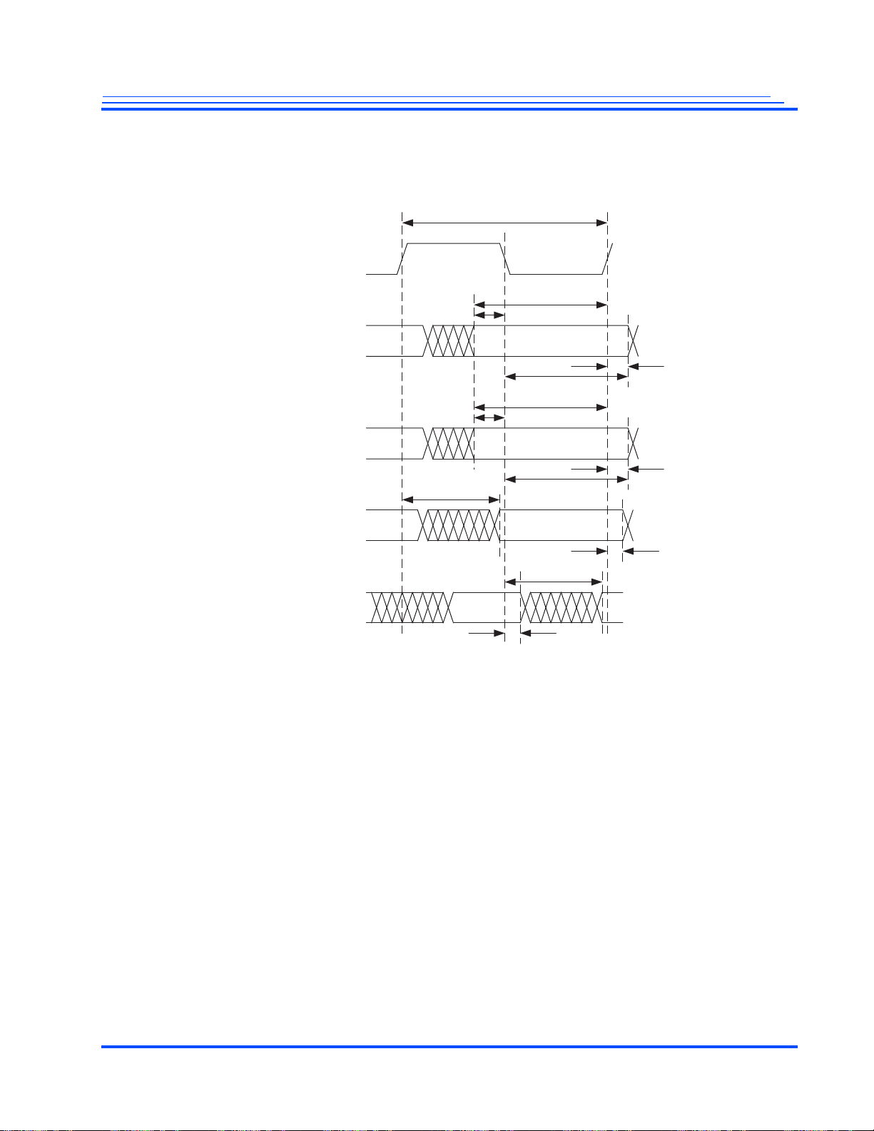
MG3500/MG2580 HD H.264 Codec SoC Data Sheet
BS_CLK
SPI_MCLK (pin)
t
CKi
t
ESUFi
BS_EN
SPI_MSS0 (pin)
t
DSURi
t
ESURi
t
DSUFi
BS_DATA
SPI_MOSI (pin)
t
RDVRi
BS_REQ
SPI_MSS1 (pin)
BS_REQ
SPI_MSS1 (pin)
t
RDVFi
t
EIHRi
t
EIHFi
t
DIHRi
t
DIHFi
t
ROHRi
t
ROHFi
BS_CLK mastered from the MG3500 SoC internal source and Data mastered by a
source external to the MG3500 SoC.
Figure 4-17 Bitstream Timing with an Internal Clock and External Data Master
Maxim Integrated Products Advance Information | 93

MG3500/MG2580 HD H.264 Codec SoC Data Sheet
Table 4-19 Bitstream Timing AC Timing Values 3
Signal Parameter Description
BS_CLK
SPI_MCLK
BS_EN
SPI_MSS0
BS_DATA
SPI_MOSI
BS_REQ
SPI_MSS1
t
CKi
t
ESUFi
t
ESURi
t
EIHFi
t
EIHRi
t
DSUFi
t
DSURi
t
DIHFi
t
DIHRi
t
RDVFi
t
RDVRi
t
ROHFi
t
ROHRi
External Clock Period 14.8
Bitstream Enable setup to falling
edge of BS_CLK
Bitstream Enable setup to rising edge
of BS_CLK
Bitstream Enable input hold from
falling edge of BS_CLK
Bitstream Enable input hold from
rising edge of BS_CLK
Bitstream Data setup to falling edge
of BS_CLK
Bitstream Data setup to rising edge
of BS_CLK
Bitstream Data input hold from falling
edge of BS_CLK
Bitstream Data input hold from rising
edge of BS_CLK
Bitstream Request data valid from
falling edge of BS_CLK
Bitstream Request data valid from
rising edge of BS_CLK
Bitstream Request output hold from
falling edge of BS_CLK
Bitstream Request output hold from
rising edge of BS_CLK
Timing Value (ns.)
Min Typ Max
2.5
2.5
0.5
0.5
2.0
2.0
0.5
0.5
5.0
5.0
2.0
2.0
94 | Advance Information Maxim Integrated Products

MG3500/MG2580 HD H.264 Codec SoC Data Sheet
BS_CLK
SPI_MCLK (pin)
t
CKi
t
EDVRi
t
RSUFi
BS_REQ
SPI_MSS1 (pin)
t
RSURi
BS_EN
SPI_MSS0 (pin)
BS_EN
SPI_MSS0 (pin)
t
EDVFi
BS_DATA
SPI_MOSI (pin)
BS_DATA
SPI_MOSI (pin)
t
DDVFi
t
DDVRi
t
EOHRi
t
EOHFi
t
DOHRi
t
DOHFi
t
RIHRi
t
RIHFi
BS_CLK mastered from the MG3500 SoC internal source and Data mastered by the
MG3500 SoC.
Figure 4-18 Bitstream Timing with an Internal Clock and Internal Data Master
Maxim Integrated Products Advance Information | 95

MG3500/MG2580 HD H.264 Codec SoC Data Sheet
Table 4-20 Bitstream Timing AC Timing Values 4
Signal Parameter Description
BS_CLK
SPI_MCLK
BS_EN
SPI_MSS0
BS_DATA
SPI_MOSI
BS_REQ
SPI_MSS1
t
CKi
t
EDVFi
t
EDVRi
t
EOHFi
t
EOHRi
t
DDVFi
t
DDVRi
t
DOHFi
t
DOHRi
t
RSUFi
t
RSURi
t
RIHFi
t
RIHRi
External Clock Period 14.8
Bitstream Enable data valid from
falling edge of BS_CLK
Bitstream Enable data valid from
rising edge of BS_CLK
Bitstream Enable output hold from
falling edge of BS_CLK
Bitstream Enable output hold from
rising edge of BS_CLK
Bitstream Data data valid from falling
edge of BS_CLK
Bitstream Data data valid from rising
edge of BS_CLK
Bitstream Data output hold from
falling edge of BS_CLK
Bitstream Data output hold from
rising edge of BS_CLK
Bitstream Request setup to falling
edge of BS_CLK
Bitstream Request setup to from
rising edge of BS_CLK
Bitstream Request input hold from
falling edge of BS_CLK
Bitstream Request input hold from
rising edge of BS_CLK
Timing Value (ns.)
Min Typ Max
5.0
5.0
2.0
2.0
4.5
4.5
2.0
2.0
1.0
1.0
0.5
0.5
96 | Advance Information Maxim Integrated Products
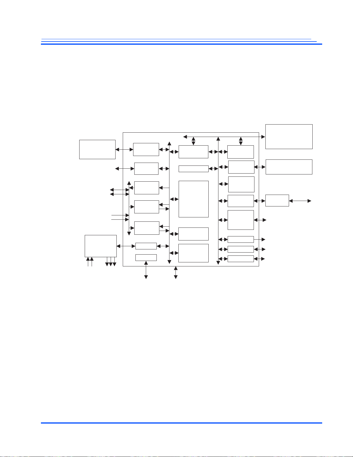
5.0 Block Level Operation
Video I/O
ITU-R BT.1120 or
ITU-R BT.656 (2X)
Video Input
ITU-R BT.1120 or
ITU-R BT.656 (2X)
DDR2 SDRAM
(1 or 2 Chips)
High-Speed
Bitstream
Two
Stereo
Inputs
XTAL
Ethernet
10/100/GigE
Ethernet
PHY
Three
Stereo
Outputs
JTAG
HD H.264
Codec
HD MPEG2
Decoder
HD JPEG
Codec
USB 2.0
PWM (3X)
UART (2X)
TWI/SPI (2X)
SDIO/MMC/
CE_ATA
SD/MMC
Controller
Master
Host
Slave Host/
Bridge
AES/SHA
Audio/
System
MME
I2S
VIP2
HD/SD
VIP1
HD/SD
VOP
HD/SD
Bitstream
I/F
SDRAM
Controller
Clocks
Audio
Codec(s)
Video MME
USB
Including
a PHY
ARM926
Processor
Ethernet
MAC
Master/ Slave Host
I/F/ NAND/NOR/
CF/IDE
16 Data, 23 Address
Serial I/O
PWM
Serial I/O
This section provides detailed block-level descriptions of each of the components, connection examples
for each of the interfaces, and programming and register information as needed.
5.1 Detailed Block Diagram
Figure 5-1 shows a detailed block diagram of the MG3500 HD H.264 Codec SoC. Refer to it as you go
through this section.
MG3500/MG2580 HD H.264 Codec SoC Data Sheet
Figure 5-1 Block Diagram of the MG3500 SoC
Maxim Integrated Products Advance Information | 97

MG3500/MG2580 HD H.264 Codec SoC Data Sheet
5.2 Reset Logic
The Reset block within the MG3500 SoC is responsible for resetting the core logic as well as the SoC
blocks that surround it.
The core reset signal consists of the power on reset signal from an external pin (RESETn), a watchdog
reset, and a software controlled chip reset signal.
5.2.1 Power On Reset
The power on reset signal comes in directly from the external RESETn pin and is asynchronous with
respect to the clock. It is assumed that the clock is not running both at the time of the assertion and deassertion of the power on reset signal.
5.2.2 WatchDog Reset
The watchdog reset is asserted when the internal watchdog logic detects an internal error. The watchdog
reset needs to be enabled before it can take effect. Resetting the watchdog timer will cause the watchdog
reset to be de-asserted, so it is self-clearing.
5.2.3 Software Chip Reset
The software chip reset is ORed with the watchdog reset. Resetting the software chip reset register cause
the software chip reset signal to be de-asserted, so it provides a form of self-clearing mechanism.
All three of these resets get combined into a signal that resets the both the core and also the SoC blocks
that surround it. In addition, there are reset registers that allow each of the blocks within the SoC logic
to be reset independently. Since control of these reset signals is done using the software API, they are
not discussed in this manual.
98 | Advance Information Maxim Integrated Products

MG3500/MG2580 HD H.264 Codec SoC Data Sheet
Divider
Divider
Divider
Core Clocks
(Multiple)
Oscillator
2
PLL 1
PLL 0
Scaler
SDRAM
Clocks
ARM Clock
Scaler
2 AHB Clock
4 APB Clock
Divider
Divider
Divider
UART Clocks
Divider
Timer Clock
Divider
SPI Clock
Divider
Bitstream Clock
Divider
TWI Clock
Divider
MMC Clock
PLL Scaler
USB Clock
USB_XIN
USB_XO
CLK_IN
CLK_SEL
Audio and Video
Clock Logic
VID0_PXCLK
VID1_PXCLK
VID2_PXCLK
VID1_OUTCLK
AUD0_MCLK
To VIN 0
To VIN 1
540 MHz
To VOUT
To AOI
and AII
To Internal Logic
VID0_OUTCLK
AUD1_MCLK
5.3 Clocks and PLLs
The MG3500 SoC internally creates over 20 clocks to minimize power consum ption and maximize
performance. All of the clocks are derived from a single 12 MHz crystal oscillator that is built into the
USB Interface block. This oscillator can be used even when the USB interface is not used.
5.3.1 Clock and PLL inputs
There are some cases where the MG3500 SoC requires a direct clock source, suc h as when the video
must be synchronized with an another video source. Typical applications use a 27 MHz. clock. There
are also some cases where the MG3500 SoC requires a direct clock source and the 12 MHz crystal input
to maintain USB functionality. The CLK_IN pin is provided for these cases, and the selection is
controlled by the configuration pin, CLK_SEL (see Figure 5-2).
Figure 5-2 Clocking Structure
Maxim Integrated Products Advance Information | 99

MG3500/MG2580 HD H.264 Codec SoC Data Sheet
5.3.2 Phase Lock Loops
The MG3500 SoC has a total of five PLLs. One PLL is included as part of the USB PHY, and is used
for USB PHY clocking and UTMI interfacing to the internal USB MAC. The remaining four PLLs are
used to generate all the remaining required clock frequencies. PLL1 is used to generate the four-phase
SDRAM clocking. PLL0 generates the codec core clocks, ARM processor, host bus clocks, and
generates the input clocks for PLL2 and PLL3. Audio and video clocks can be generated from either
PLL2 or PLL3, depending on the configuration of the multiplexers.
The remainder of the clocks are used for peripheral I/O circuitry, and are discussed in their individual
sections. Refer to the MG3500 SoC Pro grammers Guide for information on programming the clocks.
5.3.3 Video and Audio Clocks
Figure 5-3 shows the circuitry used to generate the video input, video output, and audio clocks. Each is
discussed in the sections that follow.
100 | Advance Information Maxim Integrated Products
 Loading...