

Page 1
Rev 0; 4/09
BURST ENABLE
AVDD/2
120kΩ
LNAAVDD/2
0mV
2mV
-1
MUX
BURST OUTPUT,
DUTY CYCLE, AND
PULSE COUNTER
SIGMA-DELTA
ADC
SIGMA-DELTA
ADC
DIGITAL
BANDPASS
FILTER
RAM
2K x 16
ROM
2K x 16
16 x 16
HW MULT
+ ACCUM
FLASH
8K x 16
OR
16K x 16
INTERNAL
REGULATORS
16-BIT 16-MIPS
MICROCONTROLLER
PROGRAMMABLE
PLL-BASED OSCILLATOR
VOLTAGE
REFERENCE
FULL WAVE
DETECTOR
THRESHOLD
ADJUST
SYSTEM
TIMER
TIMER 2
CRYSTAL
OSCILLATOR
16MHz (MAX)
INTERNAL
OSCILLATOR
WATCHDOG
POR/
BROWNOUT
UART
(LIN)
TIMER 1 TIMER 0
T0B_CMPOT0
DIGITAL
LOWPASS
FILTER
120kΩ
3kΩ
3kΩ
0.47µF
REFBG
0.47µF 0.47µF
REFSAR REFECHO
AIN0
BURST
ECHON
470pF
0.01µF
ECHOP
GATE5
AVDD
DVDD
GND
Rx
Tx
DVDDIO
REG3P3
REG2P5
+5.0V DVDDIO
BSP129
AVDD
330pF
THERMISTOR
BATTERY+
AIN1
AIN2
AIN3
AIN4
AIN5
FILT
T1T2
16MHz
20pF20pF
T2B
RESET
CLOCK PRESCALERS
DIVIDE BY 1 TO 128
FIFO
33nF
24kΩ
470pF
0.01µF
0.1µF
0.1µF
0.1µF
TRANSCEIVER
CONNECTOR
V+
GROUND
SIGNAL
+9V TO
+20V
MAXQ7667
MAXQ7667 USER’S GUIDE
______________________________________________________________________________________ Maxim Integrated Products i
Page 2

MAXQ7667 User’s Guide
TABLE OF CONTENTS
SECTION 1: Overview . . . . . . . . . . . . . . . . . . . . . . . . . . . . . . . . . . . . . . . . . . . . . . . . . . . . . . . . . . . .1-1
SECTION 2: Architecture . . . . . . . . . . . . . . . . . . . . . . . . . . . . . . . . . . . . . . . . . . . . . . . . . . . . . . . . . .2-1
SECTION 3: Programming . . . . . . . . . . . . . . . . . . . . . . . . . . . . . . . . . . . . . . . . . . . . . . . . . . . . . . . . .3-1
SECTION 4: Register Descriptions . . . . . . . . . . . . . . . . . . . . . . . . . . . . . . . . . . . . . . . . . . . . . . . . . .4-1
SECTION 5: General-Purpose I/O Module . . . . . . . . . . . . . . . . . . . . . . . . . . . . . . . . . . . . . . . . . . . .5-1
SECTION 6: Type 2 Timer/Counter Module . . . . . . . . . . . . . . . . . . . . . . . . . . . . . . . . . . . . . . . . . . . .6-1
SECTION 7: Schedule Timer . . . . . . . . . . . . . . . . . . . . . . . . . . . . . . . . . . . . . . . . . . . . . . . . . . . . . . .7-1
SECTION 8: UART and LIN . . . . . . . . . . . . . . . . . . . . . . . . . . . . . . . . . . . . . . . . . . . . . . . . . . . . . . . .8-1
SECTION 9: Enhanced Serial Peripheral Interface (SPI) Module . . . . . . . . . . . . . . . . . . . . . . . . . . .9-1
SECTION 10: Hardware Multiplier Module . . . . . . . . . . . . . . . . . . . . . . . . . . . . . . . . . . . . . . . . . . .10-1
SECTION 11: Test Access Port (TAP) . . . . . . . . . . . . . . . . . . . . . . . . . . . . . . . . . . . . . . . . . . . . . . .11-1
SECTION 12: In-Circuit Debug Mode . . . . . . . . . . . . . . . . . . . . . . . . . . . . . . . . . . . . . . . . . . . . . . .12-1
SECTION 13: In-System Programming/Bootloader . . . . . . . . . . . . . . . . . . . . . . . . . . . . . . . . . . . . .13-1
SECTION 14: SAR ADC Module . . . . . . . . . . . . . . . . . . . . . . . . . . . . . . . . . . . . . . . . . . . . . . . . . . .14-1
SECTION 15: Oscillator/Clock Generation . . . . . . . . . . . . . . . . . . . . . . . . . . . . . . . . . . . . . . . . . . .15-1
SECTION 16: Power-Supply/Supervisory Monitoring . . . . . . . . . . . . . . . . . . . . . . . . . . . . . . . . . . .16-1
SECTION 17: Ultrasonic Distance Measurement Module—
Burst Transmission and Echo Reception . . . . . . . . . . . . . . . . . . . . . . . . . . . . . . . . .17-1
SECTION 18: Utility ROM . . . . . . . . . . . . . . . . . . . . . . . . . . . . . . . . . . . . . . . . . . . . . . . . . . . . . . . . .18-1
SECTION 19: Instruction Set Summary . . . . . . . . . . . . . . . . . . . . . . . . . . . . . . . . . . . . . . . . . . . . . .19-1
_____________________________________________________________________________________________________________ ii
Page 3

MAXQ7667 User’s Guide
SECTION 1: OVERVIEW
The MAXQ7667 is a smart data-acquisition system based on the MAXQ®microcontroller (µC) with integrated peripheral functions for
ultrasonic, time-of-flight, distance measurement. The MAXQ processor is a high-performance reduced instruction set computing (RISC)
core µC designed for efficient peripheral multitasking applications. The MAXQ core contains a 16-bit Harvard Architecture RISC core
that executes instructions in a single clock cycle from instruction fetch to cycle completion. The MAXQ core works without the aid of
an instruction prefetch pipeline. This streamlines the entire instruction fetch, decode, and execute task, which dramatically improves
code density, memory access benchmarks, and multitasking interrupt-based latency. The MAXQ architecture was designed specifically for analog I/O and peripheral multitasking applications.
As a member of the MAXQ family of 16-bit RISC µCs, the MAXQ7667 is ideal for low-cost, low-power embedded applications such as
• Automotive Parking
• Vehicle Security
• Industrial Processing
• Automation
• Handheld Devices
The flexible, modular architecture design used in these µCs allows development of targeted products for specific applications with minimal effort.
The MAXQ7667 includes the following general-purpose peripherals: maximum 16MHz (factory default is 13.5MHz) RC oscillator, crystal oscillator support, watchdog timer, schedule timer, three general-purpose timer/counters, two 8-bit GPIO ports, SPI™ port, JTAG
port, LIN-capable UART, 12-bit ADC with five input channels, and a voltage reference. These modules are useful for communication,
diagnostics, and miscellaneous support.
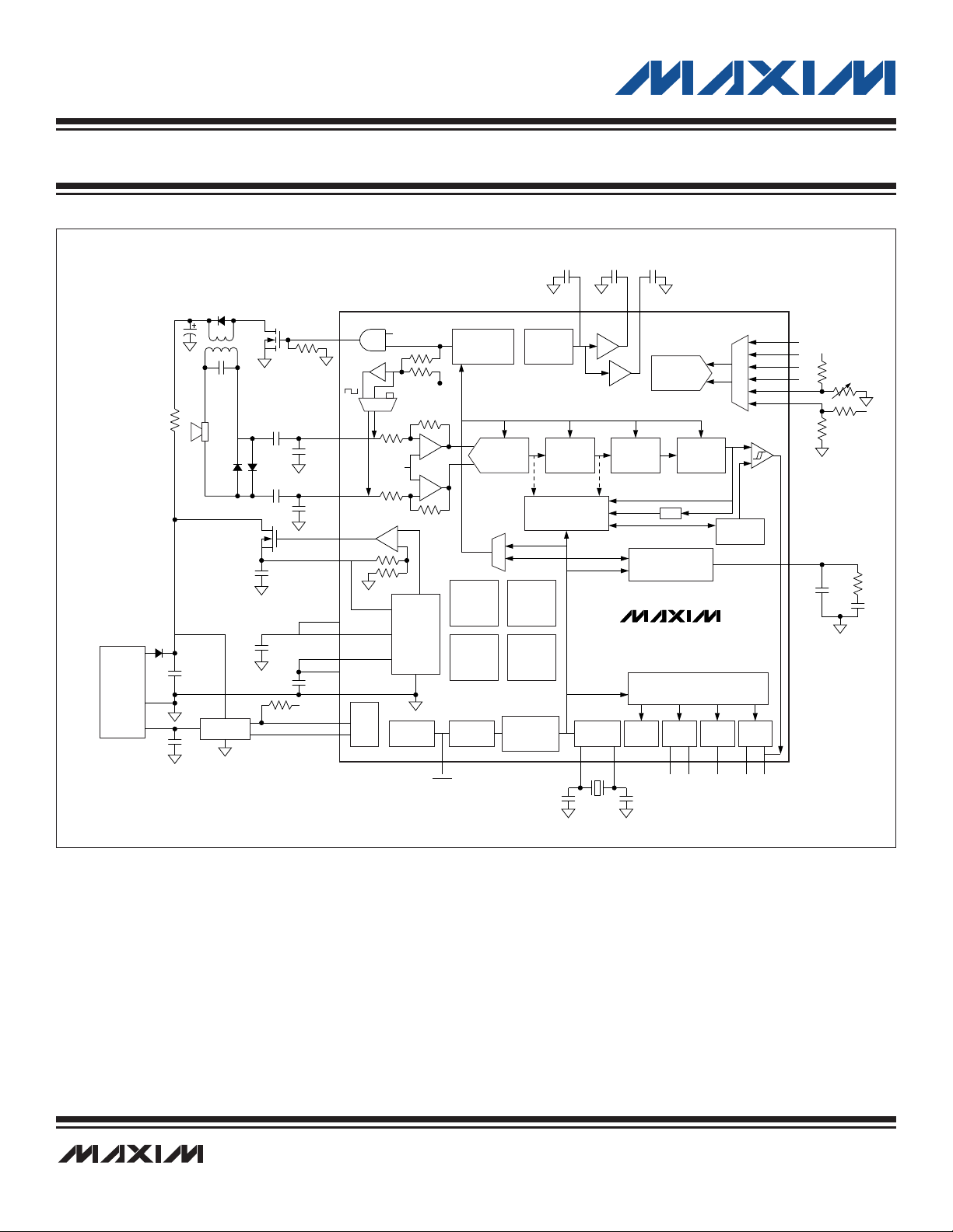
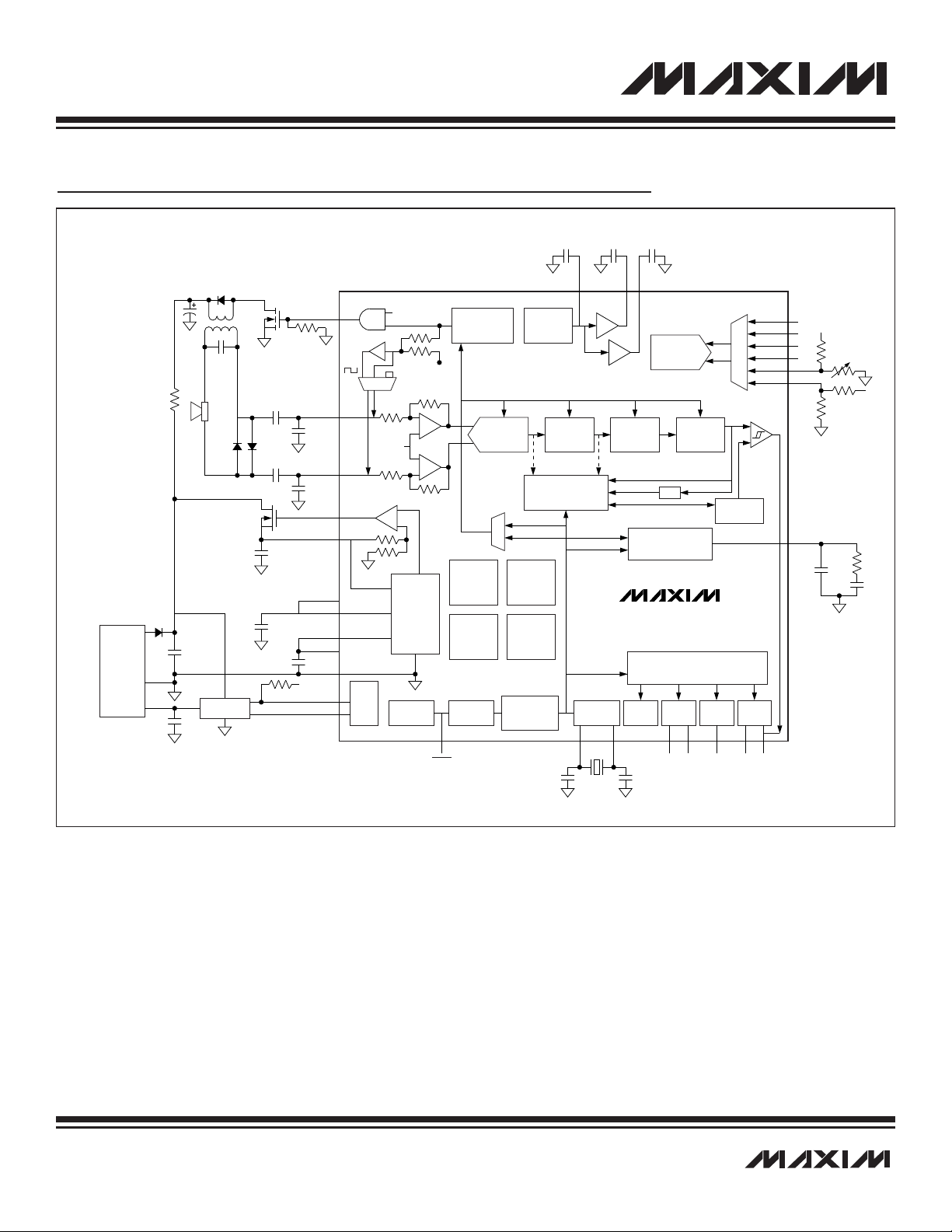
Peripherals dedicated to ultrasonic measurement include a burst signal generator and echo signal processing for transducer frequencies from 25kHz to 100kHz. When triggered, the BURST output supplies the specified number of transducer excitation cycles at
the specified frequency and duty cycle. Echo signals are received and digitized by a low noise amplifier (LNA) and 16-bit sigma-delta
ADC that together provide a variable gain ranging from 38dB to 60dB. Following the ADC is a digital bandpass filter, demodulator, and
digital lowpass filter with a 16-bit output. Supporting both the burst generator and echo reception is a programmable, PLL frequency
synthesizer that supplies both the burst frequency and the clock for the digital filters. Using the PLL for both burst transmission and
echo reception ensures that the bandpass filter always tracks the transducer excitation. Both the digital filtering and the clock synthesis are done without CPU intervention. All the CPU power is available for other tasks.
MAXQ7667 Features
• 16-Bit Single-Cycle RISC Core Processor
• Simultaneous Instruction/Data Harvard Memory Architecture
• 32KB Flash Memory
• 4KB Data RAM
• Utility ROM
• Burst-Pulse Generation Using Fractional N Frequency Synthesis
• Low-Noise, Variable Gain, Echo Receive Amplifier
16-Bit Sigma-Delta ADC for Digitizing the Echo
Digital Bandpass Filter that Tracks the Burst Frequency
Digital Demodulator and Lowpass Filter to Create an Echo Envelope with 16-Bit Resolution
FIFO Stores Up to 8 Readings from the Lowpass Filter
Digital Comparator Trips When Output of Lowpass Filter Reaches the Programmed Value
• 12-Bit, 5-Channel SAR ADC
• 2.5V Reference
MAXQ is a registered trademark of Maxim Integrated Products, Inc.
SPI is a trademark of Motorola, Inc.
___________________________________________________________________________________ Maxim Integrated Products 1-1
Page 4
• One Schedule Timer
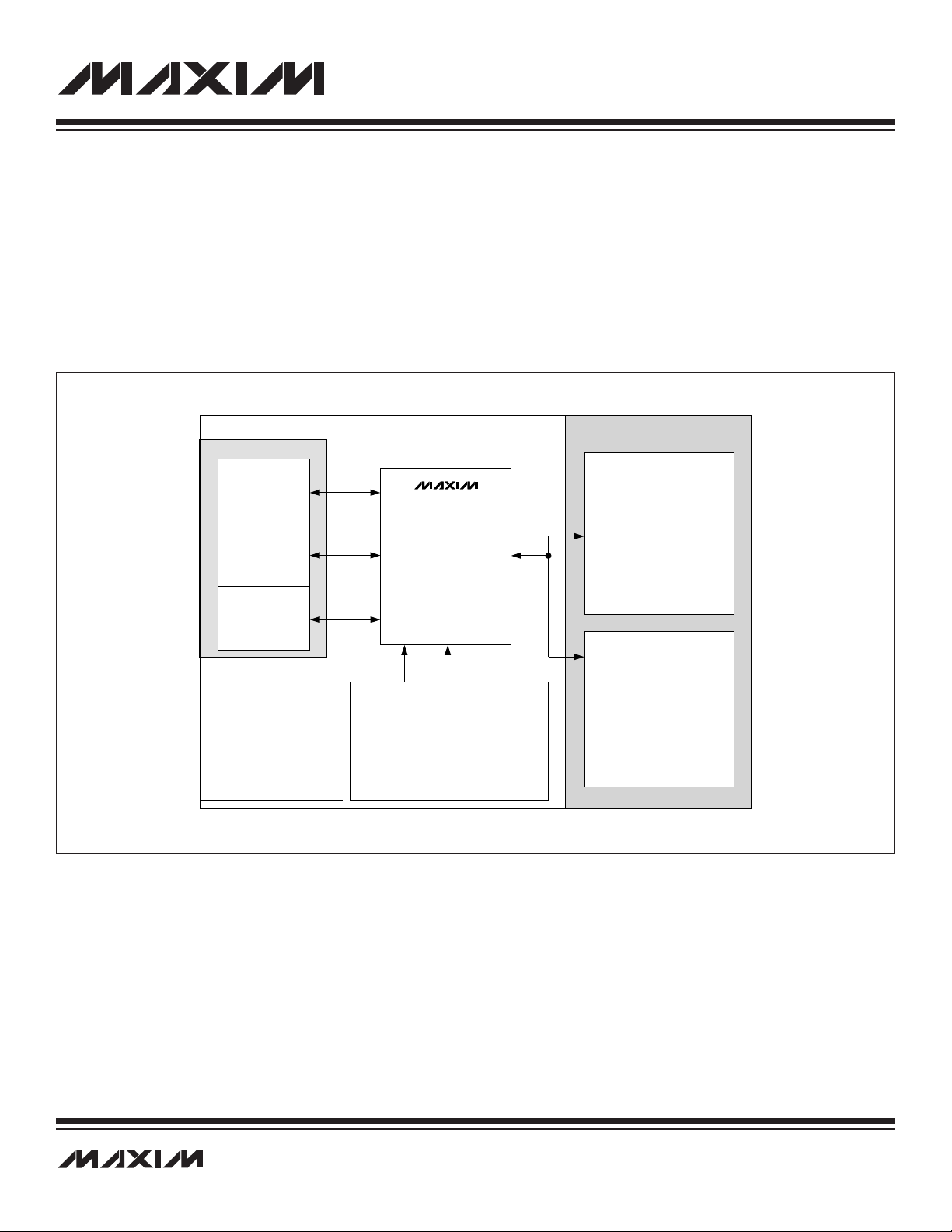
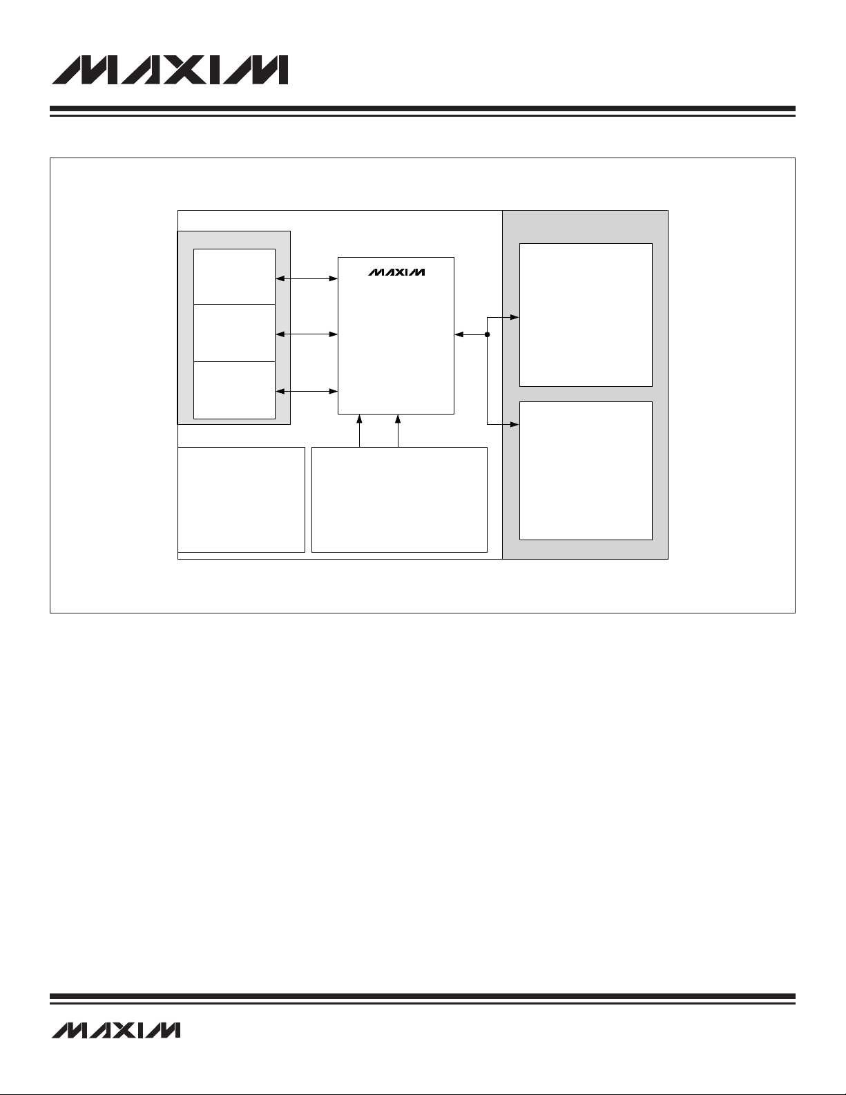
16-BIT HARVARD
MAXQ RISC CPU
•
16 ALU REGISTERS
•
MMU
•
HW MULTPLY/ACCUM
•
INTERRUPT CONTROL
•
16-WORD HW STACK
•
HARVARD ARCHITECTURE
MEMORY MODULE
CORE MODULES
CLOCK/CRYSTAL/
TIMER MODULE
•
INTERNAL 16MHz (MAX)
OSCILLATOR
•
EXTERNAL XTAL OSC
•
WATCHDOG TIMER
•
SCHEDULE TIMER
POWER MANAGEMENT
MODULE
•
+5V I/O REGULATOR
•
+3.3V ANALOG REGULATOR
•
+2.5V CORE REGULATOR
•
POWER-ON RESET
•
SUPPLY BROWNOUT DETECTORS
PERIPHERAL MODULES
GENERAL-PURPOSE
PERIPHERALS
•
3 16-BIT TIMER/PWMs
•
2 8-BIT I/O PORTS
•
UART WITH LIN 2.0 H/W
•
SPI INTERFACE
•
JTAG INTERFACE
•
12-BIT, 5-CHANNEL ADC
•
VOLTAGE REFERENCE
MAXQ7667
APPLICATION-SPECIFIC
PERIPHERALS
•
VARIABLE GAIN LNA
•
16-BIT SIGMA-DELTA ADC
•
DIGITAL BANDPASS FILTER
•
DIGITAL LOWPASS FILTER
•
LP FILTER FIFO
•
PLL FREQUENCY GENERATOR
•
BURST GENERATOR
UTILITY ROM
DATA RAM
4KB
(2KWORD)
FLASH ROM
32KB
(16KWORD)
• Three General-Purpose Timers
• LIN-Compatible UART
• SPI Port
• JTAG Port
• Watchdog Timer
• Voltage Monitors
MAXQ7667 User’s Guide
MAXQ7667 Module Functions
___________________________________________________________________________________________________________ 1-2
Page 5
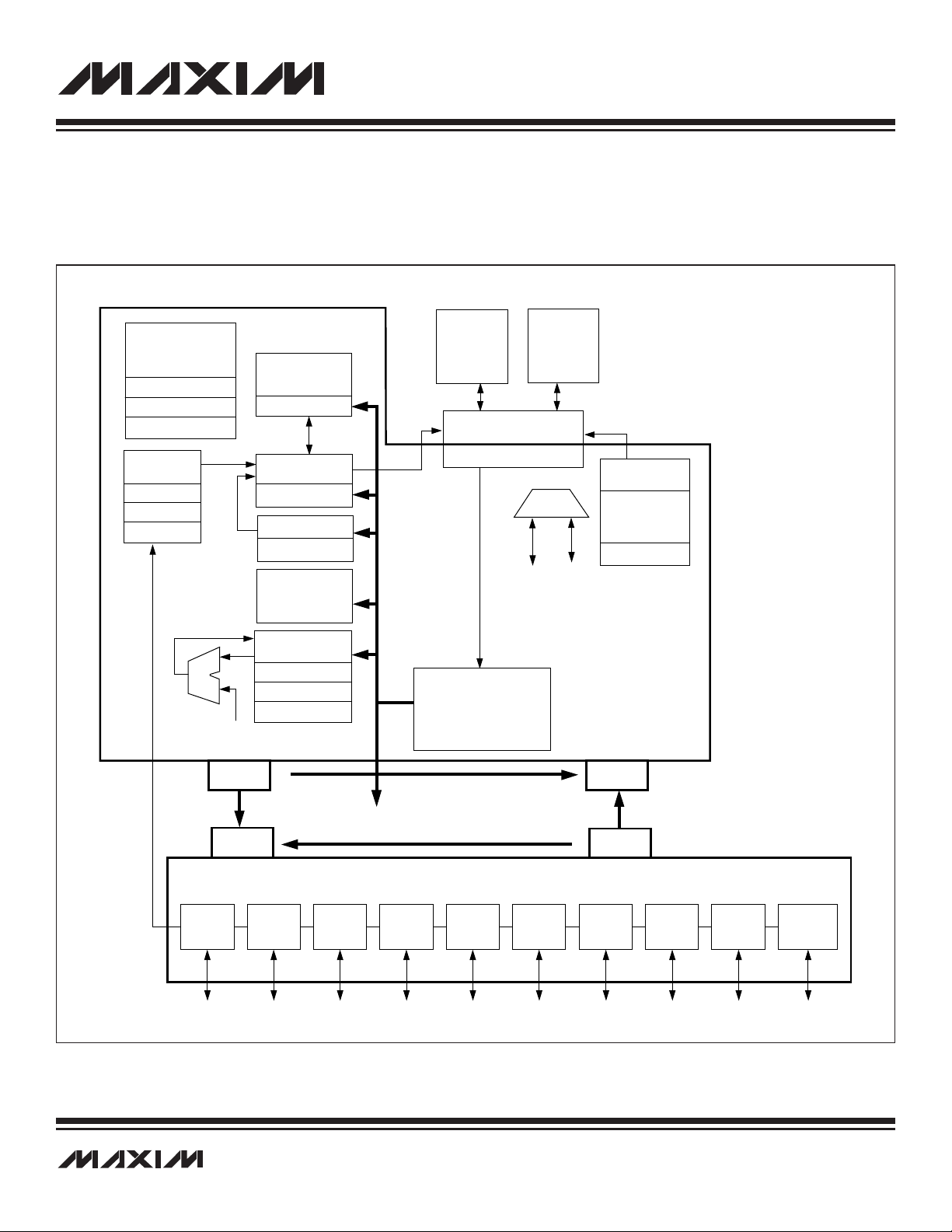
MAXQ7667 User’s Guide
BURST ENABLE
AVDD/2
120kΩ
LNAAVDD/2
0mV
2mV
-1
MUX
BURST OUTPUT,
DUTY CYCLE, AND
PULSE COUNTER
SIGMA-DELTA
ADC
SIGMA-DELTA
ADC
DIGITAL
BANDPASS
FILTER
RAM
2K x 16
ROM
2K x 16
16 x 16
HW MULT
+ ACCUM
FLASH
8K x 16
OR
16K x 16
INTERNAL
REGULATORS
16-BIT 16-MIPS
MICROCONTROLLER
PROGRAMMABLE
PLL-BASED OSCILLATOR
VOLTAGE
REFERENCE
FULL WAVE
DETECTOR
THRESHOLD
ADJUST
SYSTEM
TIMER
TIMER 2
CRYSTAL
OSCILLATOR
16MHz (MAX)
INTERNAL
OSCILLATOR
WATCHDOG
POR/
BROWNOUT
UART
(LIN)
TIMER 1 TIMER 0
T0B_CMPOT0
DIGITAL
LOWPASS
FILTER
120kΩ
3kΩ
3kΩ
0.47µF
REFBG
0.47µF 0.47µF
REFSAR REFECHO
AIN0
BURST
ECHON
470pF
0.01µF
ECHOP
GATE5
AVDD
DVDD
GND
Rx
Tx
DVDDIO
REG3P3
REG2P5
+5.0V DVDDIO
BSP129
AVDD
330pF
THERMISTOR
BATTERY+
AIN1
AIN2
AIN3
AIN4
AIN5
FILT
T1T2
16MHz
20pF20pF
T2B
RESET
CLOCK PRESCALERS
DIVIDE BY 1 TO 128
FIFO
33nF
24kΩ
470pF
0.01µF
0.1µF
0.1µF
0.1µF
TRANSCEIVER
CONNECTOR
V+
GROUND
SIGNAL
+9V TO
+20V
MAXQ7667
Typical Application Circuit
1-3 ___________________________________________________________________________________________________________
Page 6

MAXQ7667 User’s Guide
SECTION 2: ARCHITECTURE
This section contains the following information:
2.1 Overview . . . . . . . . . . . . . . . . . . . . . . . . . . . . . . . . . . . . . . . . . . . . . . . . . . . . . . . . . . . . . . . . . .2-3
2.1.1 References . . . . . . . . . . . . . . . . . . . . . . . . . . . . . . . . . . . . . . . . . . . . . . . . . . . . . . . . . .2-3
2.1.2 Instruction Set . . . . . . . . . . . . . . . . . . . . . . . . . . . . . . . . . . . . . . . . . . . . . . . . . . . . . . . .2-4
2.1.3 Harvard Memory Architecture . . . . . . . . . . . . . . . . . . . . . . . . . . . . . . . . . . . . . . . . . . . .2-5
2.1.4 Register Space . . . . . . . . . . . . . . . . . . . . . . . . . . . . . . . . . . . . . . . . . . . . . . . . . . . . . . .2-5
2.2 Architecture . . . . . . . . . . . . . . . . . . . . . . . . . . . . . . . . . . . . . . . . . . . . . . . . . . . . . . . . . . . . . . .2-6
2.2.1 Instruction Decoding . . . . . . . . . . . . . . . . . . . . . . . . . . . . . . . . . . . . . . . . . . . . . . . . . . .2-7
2.2.2 Register Space . . . . . . . . . . . . . . . . . . . . . . . . . . . . . . . . . . . . . . . . . . . . . . . . . . . . . . .2-8
2.2.3 Memory Organization . . . . . . . . . . . . . . . . . . . . . . . . . . . . . . . . . . . . . . . . . . . . . . . . . .2-10
2.2.3.1 Program Memory . . . . . . . . . . . . . . . . . . . . . . . . . . . . . . . . . . . . . . . . . . . . . . . .2-10
2.2.3.2 Utility ROM . . . . . . . . . . . . . . . . . . . . . . . . . . . . . . . . . . . . . . . . . . . . . . . . . . . .2-11
2.2.3.3 Data Memory . . . . . . . . . . . . . . . . . . . . . . . . . . . . . . . . . . . . . . . . . . . . . . . . . . .2-11
2.2.3.4 Stack Memory . . . . . . . . . . . . . . . . . . . . . . . . . . . . . . . . . . . . . . . . . . . . . . . . . .2-12
2.2.3.5 Pseudo-Von Neumann Memory Mapping . . . . . . . . . . . . . . . . . . . . . . . . . . . . .2-13
2.2.3.6 Pseudo-Von Neumann Memory Access . . . . . . . . . . . . . . . . . . . . . . . . . . . . . .2-14
2.2.3.7 Data Alignment . . . . . . . . . . . . . . . . . . . . . . . . . . . . . . . . . . . . . . . . . . . . . . . . .2-14
2.2.3.8 Memory Management Unit . . . . . . . . . . . . . . . . . . . . . . . . . . . . . . . . . . . . . . . .2-15
2.2.4 Interrupts . . . . . . . . . . . . . . . . . . . . . . . . . . . . . . . . . . . . . . . . . . . . . . . . . . . . . . . . . . . .2-18
2.2.4.1 Servicing Interrupts . . . . . . . . . . . . . . . . . . . . . . . . . . . . . . . . . . . . . . . . . . . . . .2-18
2.2.4.2 Interrupt System Operation . . . . . . . . . . . . . . . . . . . . . . . . . . . . . . . . . . . . . . . .2-18
2.2.4.3 Synchronous vs. Asynchronous Interrupt Sources . . . . . . . . . . . . . . . . . . . . . .2-19
2.2.4.4 Interrupt Prioritization by Software . . . . . . . . . . . . . . . . . . . . . . . . . . . . . . . . . .2-19
2.2.4.5 Interrupt Exception Window . . . . . . . . . . . . . . . . . . . . . . . . . . . . . . . . . . . . . . .2-19
2.2.4.6 MAXQ7667 Interrupt Sources . . . . . . . . . . . . . . . . . . . . . . . . . . . . . . . . . . . . . .2-19
___________________________________________________________________________________ Maxim Integrated Products 2-1
Page 7

MAXQ7667 User’s Guide
LIST OF FIGURES
Figure 2-1. MAXQ7667 Block Diagram . . . . . . . . . . . . . . . . . . . . . . . . . . . . . . . . . . . . . . . . . . . . .2-4
Figure 2-2. MAXQ7667 Transport-Triggered Architecture . . . . . . . . . . . . . . . . . . . . . . . . . . . . . . .2-6
Figure 2-3. Instruction Word Format . . . . . . . . . . . . . . . . . . . . . . . . . . . . . . . . . . . . . . . . . . . . . . . .2-7
Figure 2-4. Pseudo-Von Neumann Memory Map (MAXQ7667 Default) . . . . . . . . . . . . . . . . . . . .2-13
Figure 2-5. Word Access Mode in MAXQ7667 . . . . . . . . . . . . . . . . . . . . . . . . . . . . . . . . . . . . . . .2-16
Figure 2-6. Byte Access Mode in MAXQ7667 . . . . . . . . . . . . . . . . . . . . . . . . . . . . . . . . . . . . . . . .2-17
Figure 2-7. MAXQ7667 Interrupt Source Hierarchy Example . . . . . . . . . . . . . . . . . . . . . . . . . . . .2-20
LIST OF TABLES
Table 2-1. Register-to-Register Transfer Operations . . . . . . . . . . . . . . . . . . . . . . . . . . . . . . . . . . .2-8
Table 2-2. MAXQ7667 Register Modules . . . . . . . . . . . . . . . . . . . . . . . . . . . . . . . . . . . . . . . . . . . .2-9
Table 2-3. MAXQ7667 Interrupt Sources and Control Bits . . . . . . . . . . . . . . . . . . . . . . . . . . . . . .2-21
___________________________________________________________________________________________________________ 2-2
Page 8

MAXQ7667 User’s Guide
SECTION 2: ARCHITECTURE
2.1 Overview
The MAXQ7667 is a low-power, high-performance, 16-bit RISC microcontroller based on the MAXQ architecture. It includes support
for integrated, in-system-programmable flash memory and a wide range of peripherals supporting ultrasonic measurement, schedule
timer, general-purpose timer/counters, GPIO, SPI, JTAG port, LIN-capable UART, 12-bit SAR ADC with five input channels, and a voltage reference.
The MAXQ7667 key features include:
• 16-Bit Single-Cycle RISC Core Processor
• Simultaneous instruction/Data Harvard Memory Architecture
• 32KB Flash Memory
• 4KB Data RAM
• Utility ROM
• Burst Generation and Echo Reception for Ultrasonic Measurement
• 12-Bit, 5-Channel SAR ADC
• One Schedule Timer
• Three General-Purpose Timers
• LIN-Compatible UART
• SPI Port
• JTAG Port
• Watchdog Timer
• Voltage Monitors
2.1.1 References
The online MAXQ7667 QuickView page contains information and data sheet links for all parts in the MAXQ7667 family. Errata sheets
for the MAXQ products are available at
ment hardware and software, frequently asked questions and software examples, visit the MAXQ home page at
ic.com/MAXQ. For general questions and discussion of the MAXQ platform, visit our discussion board at http://discuss.dalsemi.com.
Technical Support is also available at www.maxim-ic.com/support.
www.maxim-ic.com/errata. For more information on other MAXQ microcontrollers, develop-
www.maxim-
2-3 ___________________________________________________________________________________________________________
Page 9
MAXQ7667 User’s Guide
16-BIT HARVARD
MAXQ RISC CPU
•
16 ALU REGISTERS
•
MMU
•
HW MULTPLY/ACCUM
•
INTERRUPT CONTROL
•
16-WORD HW STACK
•
HARVARD ARCHITECTURE
MEMORY MODULE
CORE MODULES
CLOCK/CRYSTAL/
TIMER MODULE
•
INTERNAL 16MHz (MAX)
OSCILLATOR
•
EXTERNAL XTAL OSC
•
WATCHDOG TIMER
•
SCHEDULE TIMER
POWER MANAGEMENT
MODULE
•
+5V I/O REGULATOR
•
+3.3V ANALOG REGULATOR
•
+2.5V CORE REGULATOR
•
POWER-ON RESET
•
SUPPLY BROWNOUT DETECTORS
PERIPHERAL MODULES
GENERAL-PURPOSE
PERIPHERALS
•
3 16-BIT TIMER/PWMs
•
2 8-BIT I/O PORTS
•
UART WITH LIN 2.0 H/W
•
SPI INTERFACE
•
JTAG INTERFACE
•
12-BIT, 5-CHANNEL ADC
•
VOLTAGE REFERENCE
MAXQ7667
APPLICATION-SPECIFIC
PERIPHERALS
•
VARIABLE GAIN LNA
•
16-BIT SIGMA-DELTA ADC
•
DIGITAL BANDPASS FILTER
•
DIGITAL LOWPASS FILTER
•
LP FILTER FIFO
•
PLL FREQUENCY GENERATOR
•
BURST GENERATOR
UTILITY ROM
DATA RAM
4KB
(2KWORD)
FLASH ROM
32KB
(16KWORD)
Figure 2-1. MAXQ7667 Block Diagram
2.1.2 Instruction Set
As part of the MAXQ family, the MAXQ7667 uses the standard 16-bit MAXQ20 instruction set, with all instructions a fixed 16 bits in
length. A register-based, transport-triggered architecture allows all instructions to be coded as simple transfer operations. All instructions reduce to either writing an immediate value to a destination register or memory location or moving data between registers and/or
memory locations.
This simple top-level instruction decoding allows all instructions to be executed in a single cycle. Since all CPU operations are performed on registers only, any new functionality can be added by simply adding new register modules. The simple instruction set also
provides maximum flexibility for code optimization by a compiler.
___________________________________________________________________________________________________________ 2-4
Page 10

MAXQ7667 User’s Guide
2.1.3 Harvard Memory Architecture
As part of the MAXQ family, the MAXQ7667 core architecture is based on the MAXQ20 design, which implements a 16-bit internal databus and ALU. Program memory, data memory, and register space on the MAXQ7667 follow the Harvard architecture model. Each type
of memory is kept separate and is accessed by a separate bus, allowing different word lengths for different types of memory. Registers
may be either 8 or 16 bits in width. Program memory is 16 bits in width to accommodate the standard MAXQ 16-bit instruction set. Data
memory is also 16 bits in width but can be accessed in 8-bit or 16-bit modes for maximum flexibility.
The MAXQ7667 includes a flexible memory management unit (MMU), which allows code to be executed from either the program flash,
the utility ROM, or the internal data SRAM. Any of these three memory spaces may also be accessed in data space at any time, with
the single restriction that whichever physical memory area is currently being used as program space cannot be read from in data
space.
2.1.4 Register Space
Since all functions in the MAXQ family are accessed through registers, common functionality is provided through a common register
set. Many of these registers provide the equivalent of higher level op codes by directly accessing the arithmetic logic unit (ALU), the
loop counter registers, and the data pointer registers. Others, such as the interrupt registers, provide common control and configuration functions that are equivalent across all MAXQ microcontrollers.
The common register set, also known as the System Registers, includes the following:
• ALU access and control registers, including working accumulator registers and the processor status flags
• Two Data Pointers and a Frame Pointer for data memory access
• Autodecrementing Loop Counters for fast, compact looping
• Instruction Pointer and other branching control access points
• Stack Pointer and an access point to the 16-bit-wide dedicated hardware stack
• Interrupt vector, identification, and masking registers
The MAXQ7667 peripheral register space (modules 0 to 5) contains registers that access the following peripherals:
• Two general-purpose, 8-bit, I/O ports (P0, P1)
• LIN-compatible UART
• Serial peripheral interface (SPI)
• Hardware multiplier
• JTAG debug engine
• Three programmable Type 2 timer/counters
• Analog module
• Schedule timer
• Burst generator
• Echo receiver path
2-5 ___________________________________________________________________________________________________________
Page 11
MAXQ7667 User’s Guide
SYSTEM MODULES/
REGISTERS
PERIPHERAL MODULES/REGISTERS
DATA
MEMORY
dst
STACK
MEMORY
CKCN
WDCN
IC
ADDRESS
GENERATION
IP
SP
IC
LOOP COUNTERS
LC[η]
IIR
IMR
INTERRUPT
LOGIC
CLOCK CONTROL,
WATCHDOG TIMER
AND POWER MONITOR
BOOLEAN
VARIABLE
MANIPULATION
ACCUMULATORS
(16)
AP
APC
PSF
INSTRUCTION
DECODE
(SRC, DST TRANSPORT
DETERMINATION)
MUX
DATA POINTERS
DP[0], DP[1]
FP =
(BP + OFFS)
DPC
SC
MEMORY MANAGEMENT
UNIT (MMU)
PROGRAM
MEMORY
src
dst
src
GENERAL-
PURPOSE
I/O
TIMERS/
COUNTERS
UART
(LIN)
SPI
ANALOG
HARDWARE
MULTIPLIER
JTAG
DEBUG
ENGINE
SCHEDULE
TIMER
CLOCK
ULTRASONIC
SOUND
MEASUREMENT
2.2 Architecture
The MAXQ7667 architecture is designed to be modular and expandable. Top-level instruction decoding is extremely simple and based
on transfers to and from registers. The registers are organized into functional modules, which are in turn divided into the system register and peripheral register groups. Figure 2-2 illustrates the modular architecture.
Figure 2-2. MAXQ7667 Transport-Triggered Architecture
___________________________________________________________________________________________________________ 2-6
Page 12

MAXQ7667 User’s Guide
FORMAT DESTINATION SOURCE
f
dddddddssssssss
Memory access from the MAXQ7667 is based on a Harvard architecture with separate address spaces for program and data memory. The simple instruction set and transport-triggered architecture allow the MAXQ7667 to run in a nonpipelined execution mode where
each instruction can be fetched from memory, decoded, and executed in a single clock cycle. Data memory is accessed through one
of three data pointer registers. Two of these data pointers, DP[0] and DP[1], are stand-alone 16-bit pointers. The third data pointer, FP,
is composed of a 16-bit base pointer (BP) and an 8-bit offset register (OFFS). All three pointers support postincrement/decrement functionality for read operations and preincrement/decrement for write operations. For the Frame Pointer (FP = BP[OFFS]), the increment/decrement operation is executed on the OFFS register and does not affect the base pointer (BP). Stack functionality is provided
by dedicated memory with a 16-bit width and depth of 16. An on-chip memory management unit (MMU) is accessible through system
registers to allow logical remapping of physical program and data spaces, and thus facilitates in-system programming and fast access
to data tables, arrays, and constants physically located in program memory.
2.2.1 Instruction Decoding
Every MAXQ7667 instruction is encoded as a single 16-bit word according to the format in Figure 2-3.
Figure 2-3. Instruction Word Format
Bit 15 (f) indicates the format for the source field of the instruction as follows:
• If f equals 0, the instruction is an immediate source instruction, and the source field represents an immediate 8-bit value.
• If f equals 1, the instruction is a register source instruction, and the source field represents the register that the source value will be
read from.
Bits 0 to 7 (ssssssss) represent the source for the transfer. Depending on the value of the format field, this can either be an immediate
value or a source register. If this field represents a register, the lower four bits contain the module specifier and the upper four bits contain the register index in that module.
Bits 8 to 14 (ddddddd) represent the destination for the transfer. This value always represents a destination register, with the lower four
bits containing the module specifier and the upper three bits containing the register subindex within that module.
Since the source field is 8 bits wide and 4 bits are required to specify the module, any one of 16 registers in that module may be specified as a source. However, the destination field has one less bit, which means that only eight registers in a module can be specified
as a destination in a single-cycle instruction.
While the asymmetry between source and destination fields of the op code may initially be considered a limitation, this space can be
used effectively. Firstly, since read-only registers will never be specified as destinations, they can be placed in the second eight locations in a module to give single-cycle read access. Secondly, there are often critical control or configuration bits associated with system and certain peripheral modules where limited write access is beneficial (e.g., watchdog-timer enable and reset bits). By placing
such bits in one of the upper 24 registers of a module, this write protection is added in a way that is virtually transparent to the assembly source code. Anytime that it is necessary to directly select one of the upper 24 registers as a destination, the prefix register PFX is
used to supply the extra destination bits. This prefix register write is inserted automatically by the assembler and requires one additional execution cycle.
The MAXQ7667 architecture is transport-triggered. This means that writing to or reading from certain register locations will also cause
side effects to occur. These side effects form the basis for the higher level op codes defined by the assembler, such as ADDC, OR,
JUMP, and so on. While these op codes are actually implemented as MOVE instructions between certain register locations, the encoding is handled by the assembler and need not be a concern to the programmer. The registers defined in the System Register and
Peripheral Register maps operate as described in the documentation; the unused "empty" locations are the ones used for these special cases.
The MAXQ7667 instruction set is designed to be highly orthogonal. All arithmetic and logical operations that use two registers can use
any register along with the accumulator. Data can be transferred between any two registers in a single instruction.
2-7 ___________________________________________________________________________________________________________
Page 13
MAXQ7667 User’s Guide
DESTINATION SET TO VALUE
SOURCE REGISTER SIZE
(BITS)
DESTINATION REGISTER
SIZE (BITS)
PREFIX SET?
HIGH 8 BITS LOW 8 BITS
88— Source [7:0]
8 16 No 00h Source [7:0]
8 16 Yes Prefix [7:0] Source [7:0]
16 8 — Source [7:0]
16 16 No Source [15:8] Source [7:0]
2.2.2 Register Space
The MAXQ7667 architecture provides a total of 16 register modules. Each of these modules contains 32 registers. Of these possible
16 register modules, only 13 are used on the MAXQ7667—seven for system registers and six for peripheral registers. The first eight
registers in each module may be read from or written to in a single cycle; the second eight registers may be read from in a single cycle
and written to in two cycles (by using the prefix register PFX); the last 16 registers may be read or written in two cycles (always requiring use of the prefix register PFX).
Registers may be either 8 or 16 bits in length. Within a register, any number of bits can be implemented; bits not implemented are fixed
at zero. Data transfers between registers of different sizes are handled as shown in Table 2-1.
• If the source and destination registers are both 8 bits wide, data is transferred bit to bit accordingly.
• If the source register is 8 bits wide and the destination register is 16 bits wide, the data from the source register is transferred
into the lower 8 bits of the destination register. The upper 8 bits of the destination register are set to the current value of the prefix register; this value is normally zero, but it can be set to a different value by the previous instruction if needed. The prefix register reverts back to zero after one cycle, so this must be done by the instruction immediately before the one that will be using
the value.
• If the source register is 16 bits wide and the destination register is 8 bits wide, the lower 8 bits of the source are transferred to
the destination register.
• If both registers are 16 bits wide, data is copied bit to bit.
Table 2-1. Register-to-Register Transfer Operations
The above rules apply to all data movements between defined registers. Data transfer to/from undefined register locations has the following behavior:
• If the destination is an undefined register, the MOVE is a dummy operation but may trigger an underlying operation according
to the source register (e.g., @DP[n]--).
• If the destination is a defined register and the source is undefined, the source data for the transfer will depend upon the source module width. If the source is from a module containing 8-bit or 8-bit and 16-bit source registers, the source data will be equal to the prefix data concatenated with 00h. If the source is from a module containing only 16-bit source registers, 0000h source data is used for
the transfer.
The 16 available register modules are broken up into two different groups. The low six modules (specifiers 0h through 5h) are known
as the Peripheral Register modules, while the high 10 modules (specifiers 6h to Fh) are known as the System Register modules. These
groupings are descriptive only, as there is no difference between accessing the two register groups from a programming perspective.
The System Registers define basic functionality that remains the same across all products based on the MAXQ architecture. This
includes all register locations that are used to implement higher-level op codes as well as the following common system features.
• ALU (MAXQ20: 16 bits) and associated status flags (zero, equals, carry, sign, overflow)
• Eight working accumulator registers (MAXQ20: 16-bit width), along with associated control registers
• Instruction pointer
• Registers for interrupt control, handling, and identification
• Autodecrementing loop counters for fast, compact looping
• Two data pointer registers and a frame pointer for data memory access
___________________________________________________________________________________________________________ 2-8
Page 14
MAXQ7667 User’s Guide
MODULE NAME (BASE SPECIF IER)
REGISTER
INDEX
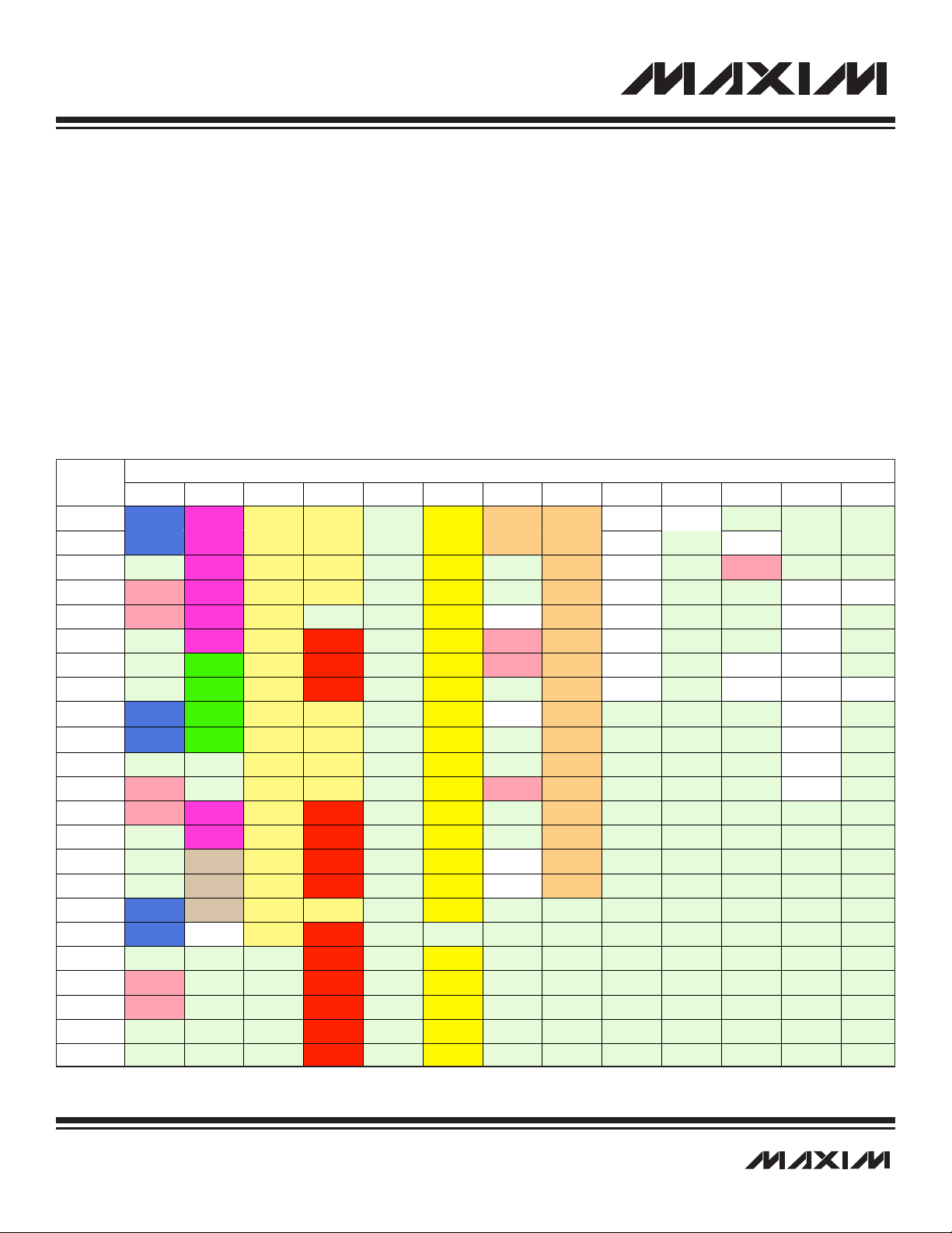
M0 M1 M2 M3 M4 M5 M8 M9 M11 M12 M13 M14 M15
00h PO0 MCNT T2CNA0 T2CNA2 BPH AP A[0] PFX[0] IP
01h PO1 MA T2H0 T2H2 BTRN APC A[1] PFX[1] SP
02h MB T2RH 0 T2RH2 SARC A[2] PFX[2] IV
03h EIF0 MC2 T2CH0 T2CH2 RCVC A[3] PFX[ 3] OFFS DP0
04h EIF1 MC1 T2CNA1 PLLF PSF A[4] PFX[4] DPC
05h MC0 T2H1 C NT1 AIE IC A[5] PFX[5] GR
06h SPIB T2RH1 SCON CMPC IMR A[6] PFX[6] LC0 GRL
07h SPICN T2CH 1 SBUF CMPT A[7] PFX[7] LC1 BP DP1
08h PI0 SPIC F T2CNB0 T2CNB2 ASR SC A[8] GRS
09h PI1 SPICK T2V0 T2V2 SARD A[9] GRH
0Ah T2R0 T2R2 LPFC A[10] GRXL
0Bh EIE0 T2C0 T2C2 OSCC IIR A[11] FP
0Ch EIE1 MC1R T2CNB1 FSTAT BPFI A[12]
0Dh MC0R T2V1 ERRR BPFO A[13]
0Eh SCNT T2R1 CHKSUM LPFD CKCN A[14]
0Fh STIM T2C1 ISVEC LPFF WDCN A[15]
10h PD0 SALM T2CFG0 T2CFG2 APE
11h PD1 FPC TL T2CFG1 STA 0
12h SMD FGAIN
13h EIES0 FCON B1COEF
14h EIES1 CNT0 B2COEF
15h CNT2 B3COEF
16h IDFB A2A
The MAXQ7667 peripheral register space (modules 0 to 5) contains registers that access the following peripherals:
• Two general-purpose, 8-bit, I/O ports (P0, P1)
• External interrupts (up to 16)
• Three programmable Type 2 timer/counters
• LIN-compatible UART interface
• SPI
• Analog module (SAR ADC and ultrasonic measurement)
• Hardware multiplier
• JTAG debug engine
• Schedule timer
The lower 8 bits of all registers in modules 0 to 5 (as well as the AP module M8) are bit addressable.
Table 2-2. MAXQ7667 Register Modules
2-9 ___________________________________________________________________________________________________________
Page 15
MODULE NAME (BASE SPECIF IER)
REGISTER
INDEX
M0 M1 M2 M3 M4 M5 M8 M9 M11 M12 M13 M14 M15
17h RCTRM† SADDR A2B
18h PS0 ICDT0 SADEN
19h PS1 ICDT1 BT A2D
1Ah ICDC T MR
1Bh PR0 ICDF A3A
1Ch PR1 ID0 ICDB A3B
1Dh ID1 ICDA
1Eh ICDD A3D
1Fh
RESERVE D
OR
OPCOD E
PORT
PINS
(GPIO)
SPI
INTERR U PT
CONTRO L
HARDWA RE
MULTIP LIE R
TIMERS
UART
(LIN)
ANALOG
I/O
ACC
ARRAY,
CONTRO L
OTHER
FUNCTIO N S
SCHED UL E
TIMER
TRIM
REGIST E R
JTAG
DEBUG
Table 2-2. MAXQ7667 Register Modules (continued)
MAXQ7667 User’s Guide
†The RCTRM register is a read/write register, but on power-up flash restores the factory-trimmed voltage. (Contact Maxim for write capability.)
2.2.3 Memory Organization
Beyond the internal register space, memory on the MAXQ7667 microcontroller is organized according to a Harvard architecture, with
a separate address space and bus for program memory and data memory. Stack memory is also separate and is accessed through
a dedicated register set.
To provide additional memory map flexibility, an MMU allows data memory space to be mapped into a predefined program memory segment, thus affording the possibility of code execution from data memory. Additionally, program memory space can be made accessible
as data space, allowing access to constant data stored in program memory. All memory is internal, and physical memory segments
(other than the stack and register memories) can be accessed as either program memory or as data memory, but not both at once.
2.2.3.1 Program Memory
The MAXQ7667 contains up to 16K x 16 (32KB) of flash memory, which normally serves as program memory. When executing from the
data SRAM or utility ROM, this memory is mapped to data space and can be used for lookup tables and similar functions. Flash memory mapped into data space can be read from directly, like any other type of data memory. However, writing to flash memory must be
done by calling the in-application functions provided by the utility ROM. The utility ROM provides routines to carry out the necessary
operations (erase, write) on flash memory.
Program memory begins at address 0000h and is contiguous through the internal program memory. The actual size of the on-chip program memory available for user application is product dependent. Given a 16-bit program address bus, the maximum program space
is 64KWords. Since the codewords are 16 bits, the program memory is therefore a 64K x 16 linear space.
Program memory is accessed directly by the program fetching unit and is addressed by the Instruction Pointer register. From an implementation perspective, system interrupts and branching instructions simply change the contents of the Instruction Pointer and force
the op code fetch from a new program location. The Instruction Pointer is direct read/write accessible by the user software; write access
to the Instruction Pointer will force program flow to the new address on the next cycle following the write. The contents of the Instruction
Pointer will be incremented by 1 automatically after each fetch operation. The Instruction Pointer defaults to 8000h, which is the start-
__________________________________________________________________________________________________________ 2-10
Page 16

MAXQ7667 User’s Guide
ing address of the utility ROM. The default IP setting of 8000h is assigned to allow initial in-system programming to be accomplished
with utility ROM code assistance. The utility ROM code interrogates a specific register bit in order to decide whether to execute in-system programming or jump immediately to user code starting at 0000h. The user code reset vector should always be stored in the lowest bytes of the program memory.
2.2.3.2 Utility ROM
A utility ROM (4K x 16) is normally placed in the upper 32KWord program memory space starting at address 8000h. This utility ROM
potentially provides the following system utility functions:
• Reset vector
• Bootstrap function for system initialization
• In-application programming
• In-circuit debug
Following each reset, the processor automatically starts execution at address 8000h in the utility ROM, allowing ROM code to perform
any necessary system support functions.
After a reset, the MAXQ7667 instruction pointer jumps to the ROM bootloader (0x8000). At this point the password location gets
checked for a valid entry. If the password space (0x0010 to 0x001F) in flash is populated by all 0s or 1s (implying that no password
has been set), the PWL bit (in SC register) is set to 0, allowing access to all the bootloader functions. Otherwise, the PWL bit gets set
to 1, preventing access to the password-protected family of commands (more on this later) and eventually the user must provide the
password to clear PWL to access all the bootloader functions.
The processor then looks for a request from the JTAG port. The JTAG port is established as the programming port before the MAXQ7667
is released from reset. While the MAXQ7667 is in reset, the SPE bit is set to 1 via the JTAG/TAP port. If the request is valid (i.e., SPE =
1, PSS = 00), the processor establishes communication between the ROM bootloader and the JTAG port. Otherwise, the UART is monitored for an autobaud character: 0x0D (carriage return). If the autobaud character is detected, the UART is established as the bootloader communication port and the MAXQ7667 responds with 0x3E. 0x3E is the acknowledgement that a loader command has been
completed. After this, some or all of the bootloader functions are accessible through the UART, depending on password settings.
The processor jumps to the flash program space 0x0000 and starts executing application code when there is no JTAG request and a
valid password is found (PWL =1). The code execution also jumps to 0x0000 when the autobaud routine does not receive the 0x0D
character within the 5-second built-in wait.
It is still possible to load a new program through the UART or the JTAG, after the MAXQ7667 begins executing code in the flash program space. To load code through the JTAG would merely require resetting the device and holding the device in reset while the SPE
bit is set to 1 through the JTAG/TAP port, once the reset is released the device executes in the bootloader (SPE = 1, PSS = 00). To load
new code through the UART would require the application code to call the UARTloader function in the utility ROM, which eventually
passes control to the bootloader (more on this later).
If the MAXQ7667’s password-protection feature is being used, it is important to note that setting the PWL (password lock) bit to 0
makes the MAXQ7667 vulnerable to attacks. It is recommended that after a communication link is established between the host and
the MAXQ7667, the Password Match command (03h) be executed to access the password-protected family of commands.
2.2.3.3 Data Memory
The MAXQ7667 contains 2K x 16 (4096 bytes) of on-chip data SRAM that can be mapped into either program or data space. The contents of this SRAM are indeterminate after power-on reset, but are maintained during stop mode and across non-POR resets, as long
as the DVDD (CORE) supply stays within the acceptable range.
On-chip data memory begins at address x0000h and is contiguous through the internal data memory. Data memory is accessed via
indirect register addressing through a Data Pointer (@DP[n]) or Frame Pointer (@BP[OFFS]). The Data Pointer is used as one of the
operands in a MOVE instruction. If the Data Pointer is used as source, the core performs a Load operation that reads data from the
data memory location addressed by the Data Pointer. If the Data Pointer is used as destination, the core executes a Store operation
that writes data to the data memory location addressed by the Data Pointer. The Data Pointer can be directly accessed by the user
software.
The core incorporates two 16-bit Data Pointers (DP[0] and DP[1]) to support data memory accessing. All Data Pointers support indirect addressing mode and indirect addressing with autoincrement or autodecrement. Data Pointers DP[0] and DP[1] can be used as
post increment/decrement source pointers by a MOVE instruction or pre increment/decrement destination pointers by a MOVE instruc-
2-11 __________________________________________________________________________________________________________
Page 17

MAXQ7667 User’s Guide
tion. Using Data Pointer indirectly with "++" will automatically increase the content of the active Data Pointer by 1 immediately following the execution of read data transfer (@DP[n]++) or immediately preceding the execution of a write operation (@++DP[n]). Using
Data Pointer indirectly with "--" will decrease the content of the active Data Pointer by 1 immediately following the execution of read
data transfer (@DP[n]--) or immediately preceding the execution of a write operation (@--DP[n]).
The Frame Pointer (BP[OFFS]) is formed by 16-bit unsigned addition of Frame Pointer Base Register (BP) and Frame Pointer Offset
Register (OFFS). Frame Pointer can be used as a post increment/decrement source pointer by a MOVE instruction or as a pre increment/decrement destination pointer. Using Frame Pointer indirectly with "++" (@BP[++OFFS] for a write or @BP[OFFS++] for a read) will
automatically increase the content of the Frame Pointer Offset by 1 immediately before or after the execution of data transfer depending
upon whether it is used as a destination or source pointer respectively. Using Frame Pointer indirectly with "--" (@BP[--OFFS] for a write or
@BP[OFFS--] for a read) will decrease the content of the Frame Pointer Offset by 1 immediately before/after execution of data transfer
depending upon whether it is used as a destination or source pointer respectively. Note that the increment/decrement function affects the
content of the OFFS register only, while the contents of the BP register remain unaffected by the borrow/carry out from the OFFS register.
A data memory cycle contains only one system clock period to support fast internal execution. This allows read or write operations on
SRAM to be completed in one clock cycle. Data memory mapping and access control are handled by the MMU. Read/write access to
the data memory can be in word or in byte.
When using the in-circuit debugging features of the MAXQ7667, the top 32 bytes (bytes 0x7D0 to 0x7FF) of the SRAM must be reserved
for saved state storage and working space for the debugging routines in the utility ROM. If in-circuit debug will not be used, the entire
SRAM is available for application use.
2.2.3.4 Stack Memory
The MAXQ7667 provides a 16 x 16 hardware stack to support subroutine calls and system interrupts. A 16-bit wide on-chip stack is
provided by the MAXQ7667 for storage of program return addresses and general-purpose use. The stack is used automatically by the
processor when the CALL, RET, and RETI instructions are executed and when an interrupt is serviced; it can also be used explicitly to
store and retrieve data by using the @SP- - source, @++SP destination, or the PUSH, POP, and POPI instructions. The POPI instruction acts identically to the POP instruction except that it additionally clears the INS bit.
The width of the stack is 16 bits to accommodate the instruction pointer size. The stack depth is 16 for the MAXQ7667. As the stack
pointer register SP is used to hold the index of the top of the stack, the maximum size of the stack allowed is defined by the number
of bits defined in the SP register (e.g., 4 bits for stack depth of 16).
On reset, the stack pointer SP initializes to the top of the stack (e.g. 0Fh for a 16-word stack). The CALL, PUSH, and interrupt vectoring operations increment SP and then store a value at @SP. The RET, RETI, POP, and POPI operations retrieve the value at @SP and
then decrement SP.
As with the other RAM-based modules, the stack memory is initialized to indeterminate values upon reset or power-up. Stack memory
is dedicated for stack operations only and cannot be accessed through program or data address spaces.
When using the in-circuit debugging features of the MAXQ7667, one word of the stack must be reserved to store the return location
when execution branches into the debugging routines in the utility ROM. If in-circuit debug will not be used, the entire stack is available for application use.
__________________________________________________________________________________________________________ 2-12
Page 18
MAXQ7667 MEMORY MAP (DEFAULT CONDITION, UPA = 0)
0x0000
0x8000
0x9000
0x800
DATA MEMORY
0
15
LOGICAL SPACE
0xFFFF
PHYSICAL PROGRAM
(P0)
UTILITY ROM
LOGICAL SPACE
0x0000
0x8000
0x4000
0xA000
0xFFFF
0xA800
0x9000
PROGRAM MEMORY
15 0
LOGICAL SPACE
PHYSICAL DATA
MAXQ7667 User’s Guide
2.2.3.5 Pseudo-Von Neumann Memory Mapping
The MAXQ7667 supports a pseudo-Von Neumann memory structure that can merge program and data into a linear memory map. This
is accomplished by mapping the data memory into the program space or mapping program memory segment into the data space. In
all MAXQ processors the program memory ranges from x0000h to x7FFFh is the normal user code segment, followed by the utility ROM
segment. The uppermost part of the 64KWord memory is the logical area for data memory when accessed as a code segment.
The program memory is logically divided into four program pages, in all MAXQ processors:
• P0 contains the lower 16KWords (available in MAXQ7667),
• P1 contains the second 16KWords (not available in MAXQ7667),
• P2 contains the third 16KWords (not available in MAXQ7667), and
• P3 contains the fourth 16KWords (not available in MAXQ7667).
The MAXQ7667 only has 16K of P0 space and hence the focus will be on P0.
The logical mapping of physical program memory page(s) into data space depends upon two factors: physical memory currently in
use for program execution; and word/byte data memory access selection. If execution is from the utility ROM, physical program memory page (P0) can logically be mapped to the upper half of data memory space. If logical data memory is used for execution, physical program memory page can logically be mapped to the lower half of data memory space.
Figure 2-4 summarizes the default memory maps for this memory structure. The primary difference lies in the reset default settings for
the data pointer Word/Byte Mode Select (WBSn) bits. The WBSn bits of the MAXQ7667 default to word access mode (WBSn = 1).
Figure 2-4. Pseudo-Von Neumann Memory Map (MAXQ7667 Default)
2-13 __________________________________________________________________________________________________________
Page 19

MAXQ7667 User’s Guide
2.2.3.6 Pseudo-Von Neumann Memory Access
The pseudo-Von Neumann memory mapping is straightforward if there is no memory overlapping among the program, utility ROM, and
data memory segments. When accessing the program memory as data, the CDA bit can be used to select the program pages as needed. Full data memory access to the physical program memory pages is based on the assumption that the maximum physical data memory is in the range of 16K x 16. The other restriction for accessing the pseudo-Von Neumann map is that when program execution is in a
particular memory segment, the same memory segment cannot be simultaneously accessed as data.
When executing from the lower 16K program space (P0):
• The physical data memory is available for accessing as a code segment with offset at xA000h if the UPA bit is 0.
• Load and Store operations addressed to physical data memory are executed as normal.
• The utility ROM can be read as data, starting at x8000h of the data space.
When executing from the utility ROM:
• The lower 16K program space (P0) functions as normal program memory.
• The physical data memory is available for accessing as a code segment with offset at xA000h.
• Load and Store operations addressed to physical data memory are executed as normal.
• The 16K program space, P0, can be accessed as data, either in byte mode or word mode, with offset at 8000h.
When executing from the data memory:
• Program flows freely between the lower 16K user code (P0) and the utility ROM segment.
• The utility ROM can be accessed as data with offset at x8000h.
• The 16K program space, P0, can be accessed as data, either in byte mode or word mode, with offset at 0000h.
2.2.3.7 Data Alignment
To support merged program and data memory operation while maintaining efficiency on memory space usage, the data memory must
be able to support both byte-wide and word-wide accessing. Data is aligned in data memory as word, but the effective data address is
resolved to bytes. This data alignment allows direct program fetching in its native word size while maintaining accessibility at the byte
level. It is important to realize that this accessibility requires strict word alignment. All executable words must align to an even address
in byte mode. Care must be taken when updating the code segment in the unified data memory space as misalignment of words will
likely result in loss of program execution control. Worst yet, this situation may not be detected if the watchdog timer is also disabled.
Data memory is organized as two byte-wide memory banks with common word address decode but two 8-bit data buses. The data
memory will always be read as a complete word, independent of operation, whether program fetch or data access. The program
decoder always uses the full 16-bit word, whereas the data access can utilize a word or an individual byte.
In byte mode, data pointer hardware reads out the word containing the selected byte using the effective data word address pointer
(the least significant bit of the byte data pointer is not initially used). Then, the least significant data pointer bit functions as the byte
select that is used to place the target byte to the data path. For write access, data pointer hardware addresses a particular word using
the effective data word address while the least significant bit selects the corresponding data bank for write, leaving the contents of the
another memory bank unaffected.
__________________________________________________________________________________________________________ 2-14
Page 20

MAXQ7667 User’s Guide
2.2.3.8 Memory Management Unit
Memory allocation and accessing control for program and data memory can be managed by the memory management unit (MMU). A
single memory management unit option is discussed in this user’s guide, however the memory management unit implementation for
any given product depends upon the type and amount of memory addressable by the device. Users should consult the individual product data sheet(s) and/or user’s guide supplement(s) for detailed information.
Although supporting less than the maximum addressable program and data memory segments, the MMU implementation presented
provides a high degree of programming and access control flexibility. It supports the following:
• User program memory up to 32K x 16 (up to 64K x 16 with inclusion of UPA bit).
• Utility ROM up to 8K x 16.
• Data memory SRAM up to 16K x 16.
• In-system and in-application programming of embedded EEPROM, flash, or SRAM memories.
• Access to any of the three memory areas (SRAM, code memory, utility ROM) using the data memory pointers.
• Execution from any of the three memory areas (SRAM, code memory, factory written and tested utility-ROM routines).
Given these capabilities, the following rules apply to the memory map:
• A particular memory segment cannot be simultaneously accessed as both program and data.
• The offset address is xA000h when logically mapping data memory into the program space.
• The offset for logically mapping the utility ROM into the data memory space is x8000h.
• Program memory:
- The lower half of the program memory (P0 and P1) is always accessible, starting at x0000h. (
MAXQ7667.)
- The upper half of the program memory (P2 and P3) must be activated by setting the UPA bit to 1 when accessing for code
execution, starting at x8000h. (
- Setting the UPA bit to 1 disallows access to the utility ROM and logical data memory as program.
- Physical program memory pages (P0, P1, P2, P3) are logically mapped into data space based upon the memory segment
currently being used for execution, selection of byte/word access mode, and CDA1:0 bit settings (described in the
Von Neumann Memory Map
MAXQ7667 because it has only P0.)
• Data memory
- Access can be either word or byte.
- All 16 data pointer address bits are significant in either access mode (word or byte).
Note: P2 and P3 are not available in the MAXQ7667.)
and Pseudo-Von Neumann Memory Access sections). (Note: This does not apply to the
Note: P1 is not available in the
Pseudo-
2-15 __________________________________________________________________________________________________________
Page 21
x0000
x8000
x4000
DATA MEMORYPROGRAM MEMORY
0
15
LOGICAL SPACE
EXECUTING FROM LOGICAL DATA MEMORY (UPA = 0, ONLY P0 PRESENT)
LOGICAL UTILITY ROM
xFFFF
0x4000
PHYSICAL PROGRAM
(P0)
UTILITY ROM
CDA1 = 0
x0000
x8000
xA000
xFFFF
0xA800
15 0
LOGICAL SPACE
LOGICAL DATA MEMORY
x9000
LOGICAL SPACE
PHYSICAL DATA
x0000
x8000
xC000
0x800
DATA MEMORY
0
15
CDA1 = 0
EXECUTING FROM UTILITY ROM (UPA = 0, ONLY P0 PRESENT)
PHYSICAL PROGRAM
(P0)
UTILITY ROM
x0000
0x4000
x8000
xA000
x9000
xFFFF
0xA800
PROGRAM MEMORY
15 0
LOGICAL SPACE
LOGICAL DATA
MEMORY
LOGICAL SPACE
x0000
0x8000
0x9000
0x800
DATA MEMORYPROGRAM MEMORY
0
15
EXECUTING FROM PROGRAM SPACE (UPA = 0, ONLY P0 PRESENT)
UTILITY ROM
0xFFFF
0x4000
PHYSICAL PROGRAM
(P0)
PHYSICAL DATA
UTILITY ROM
0x0000
0x8000
0xA000
0xFFFF
0xA800
150
LOGICAL SPACE
LOGICAL DATA MEMORY
0x9000
LOGICAL SPACE
MAXQ7667 User’s Guide
Figure 2-5. Word Access Mode in MAXQ7667
__________________________________________________________________________________________________________ 2-16
Page 22
MAXQ7667 User’s Guide
UTILITY ROM
PHYSICAL DATA
x0000
x8000
xA000
x9000
xFFFF
0xA800
0x4000
x0000
x8000
0x1000
xFFFF
DATA MEMORYPROGRAM MEMORY
150 07
CDA0 = 0
EXECUTING FROM UTILITY ROM (UPA = 0, ONLY P0 PRESENT)
LOGICAL SPACE
LOGICAL SPACE
LOGICAL SPACE
LOGICAL DATA
MEMORY
PHYSICAL PROGRAM
(P0)
0x4000
PHYSICAL PROGRAM
(P0)
UTILITY ROM
x0000
x8000
xA000
xFFFF
0xA800
x0000
x8000
xFFFF
xA000
DATA MEMORYPROGRAM MEMORY
15 0
07
CDA0 = 0
EXECUTING FROM LOGICAL DATA MEMORY (UPA = 0, ONLY P0 PRESENT)
LOGICAL SPACE
LOGICAL DATA
MEMORY
LOGICAL SPACE
x9000
LOGICAL SPACE
PHYSICAL DATA
0x0000
0x8000
0xA000
0x1000
DATA MEMORY
0
7
EXECUTING FROM PROGRAM SPACE (UPA = 0, ONLY P0 PRESENT)
PHYSICAL PROGRAM
(P0)
UTILITY ROM
0x0000
0x4000
0x8000
0xA000
0x9000
0xFFFF 0xFFFF
0xA800
PROGRAM MEMORY
150
LOGICAL SPACE
LOGICAL DATA
MEMORY
LOGICAL SPACE
Figure 2-6. Byte Access Mode in MAXQ7667
2-17 __________________________________________________________________________________________________________
Page 23

MAXQ7667 User’s Guide
2.2.4 Interrupts
The MAXQ7667 provides a single, programmable interrupt vector (IV) that can be used to handle internal and external interrupts.
Interrupts can be generated from system level sources (e.g., watchdog timer) or by sources associated with the peripheral modules
included in the specific MAXQ7667 microcontroller. Only one interrupt can be handled at a time, and all interrupts naturally have the
same priority. A programmable interrupt mask register allows software-controlled prioritization and nesting of high-priority interrupts.
2.2.4.1 Servicing Interrupts
For the MAXQ7667 to service an interrupt, interrupts must be enabled globally, modularly, and locally. The Interrupt Global Enable (IGE)
bit located in the Interrupt Control (IC) register acts as a global interrupt mask. This bit defaults to 0, and it must be set to 1 before any
interrupt takes place.
The local interrupt-enable bit for a particular source is in one of the peripheral registers associated with that peripheral module, or in a
system register for any system interrupt source. Between the global and local enables are intermediate per-module and system interrupt
mask bits. These mask bits reside in the Interrupt Mask system register. By implementing intermediate per-module masking capability in
a single register, interrupt sources spanning multiple modules can be selectively enabled/disabled in a single instruction. This promotes
a simple, fast, and user-definable interrupt prioritization scheme. The interrupt source-enable hierarchy is illustrated in Figure 2-7.
When an interrupt condition occurs, its individual flag is set, even if the interrupt source is disabled at the local, module, or global level.
Interrupt flags must be cleared within the user interrupt routine to avoid repeated interrupts from the same source.
Since all interrupts vector to the address contained in the Interrupt Vector (IV) register, the Interrupt Identification Register (IIR) may be
used by the interrupt service routine to determine the module source of an interrupt. The IIR contains a bit flag for each peripheral module and one flag associated with all system interrupts; if the bit for a module is set, then an interrupt is pending that was initiated by
that module. If a module is capable of generating interrupts for different reasons, then peripheral register bits inside the module provide a means to differentiate among interrupt sources.
The Interrupt Vector (IV) register provides the location of the interrupt service routine. It may be set to any location within program memory. The IV register defaults to 0000h on reset or power-up, so if it is not changed to a different address, the user program must determine whether a jump to 0000h came from a reset or interrupt source. Note that the password starts at 0x0010, thus leaving 16 words
of programming space between the interrupt vector and the password, if 0000h is used as the IV value. (See Sections 12 and 13 for
details on password handling.)
2.2.4.2 Interrupt System Operation
The interrupt handler hardware responds to any interrupt event when it is enabled. An interrupt event occurs when an interrupt flag is
set. All interrupt requests are sampled at the rising edge of the clock and can be serviced by the processor one clock cycle later,
assuming the request does not hit the interrupt exception window. The one-cycle stall between detection and acknowledgement/servicing is due to the fact that the current instruction may also be accessing the stack. For this reason, the CPU must allow the current
instruction to complete before pushing the stack and vectoring to IV. If an interrupt exception window is generated by the currently executing instruction, the following instruction must be executed, so the interrupt service routine will be delayed an additional cycle.
Interrupt operation in the MAXQ7667 CPU is essentially a state machine generated long CALL instruction. When the interrupt handler
services an interrupt, it temporarily takes control of the CPU to perform the following sequence of actions:
1) The next instruction fetch from program memory is cancelled.
2) The return address is pushed on to the stack.
3) The INS bit is set to 1 to prevent recursive interrupt calls.
4) The instruction pointer is set to the location of the interrupt service routine (contained in the Interrupt Vector register).
5) The CPU begins executing the interrupt service routine.
Once the interrupt service routine completes, it should use the RETI instruction to return to the main program. Execution of RETI
involves the following sequence of actions:
1) The return address is popped off the stack.
2) The INS bit is cleared to 0 to re-enable interrupt handling.
3) The instruction pointer is set to the return address that was popped off the stack.
4) The CPU continues execution of the main program.
Pending interrupt requests will not interrupt an RETI instruction; a new interrupt will be serviced after first being acknowledged in the
execution cycle which follows the RETI instruction and then after the standard one stall cycle of interrupt latency. This means there will
be at least two cycles between back-to-back interrupts.
__________________________________________________________________________________________________________ 2-18
Page 24

MAXQ7667 User’s Guide
2.2.4.3 Synchronous vs. Asynchronous Interrupt Sources
Interrupt sources can be classified as either asynchronous or synchronous. All internal interrupts are synchronous interrupts. An internal
interrupt is directly routed to the interrupt handler that can be recognized in one cycle. All external interrupts are asynchronous interrupts
by nature. When the device is not in stop mode, asynchronous interrupt sources are passed through a 3-clock sampling/glitch filter circuit before being routed to the interrupt handler. The sampling/glitch filter circuit is running on the undivided source clock (i.e., before
PMME, CD[1:0]-controlled clock divide) such that the number of system clocks required to recognize an asynchronous interrupt request
depends upon the system clock divide ratio:
• if the system clock divide ratio is 1, the interrupt request is recognized after 3 system clock
• if the system clock divide ratio is 2, the interrupt request is recognized after 2 system clock (unavailable in MAXQ7667)
• if the system clock divide ratio is 4 or greater, the interrupt request is recognized after 1 system clock (unavailable in MAXQ7667)
An interrupt request with a pulse width less than three undivided clock cycles is not recognized. Note that the granularity of interrupt
source is at module level. Synchronous interrupts and sampled asynchronous interrupts assigned to the same module product a single interrupt to the interrupt handler.
External interrupts, when enabled, can be used as switchback sources from power management mode. There is no latency associated with the switchback because the circuit is being clocked by an undivided clock source versus the divide-by-256 system clock. For
the same reason, there is no latency for other switchback sources that do not qualify as interrupt sources.
2.2.4.4 Interrupt Prioritization by Software
All interrupt sources of the MAXQ7667 microcontroller naturally have the same priority. However, when CPU operation vectors to the programmed Interrupt Vector address, the order in which potential interrupt sources are interrogated is left entirely up to the user, as this
often depends upon the system design and application requirements. The Interrupt Mask system register provides the ability to knowingly block interrupts from modules considered to be of lesser priority and manually re-enable the interrupt servicing by the CPU (by setting INS = 0). Using this procedure, a given interrupt service routine can continue executing, only to be interrupted by higher priority
interrupts. An example demonstrating this software prioritization is provided in
Section 3.8: Handling Interrupts.
2.2.4.5 Interrupt Exception Window
An interrupt exception window is a noninterruptable execution cycle. During this cycle, the interrupt handler does not respond to any interrupt requests. All interrupts that would normally be serviced during an interrupt exception window are delayed until the next execution cycle.
Interrupt exception windows are used when two or more instructions must be executed consecutively without any delays in between.
Currently, there is a single condition in the MAXQ7667 microcontroller that causes an interrupt exception window: activation of the prefix (PFX) register.
When the prefix register is activated by writing a value to it, it retains that value only for the next clock cycle. For the prefix value to be
used properly by the next instruction, the instruction that sets the prefix value and the instruction that uses it must always be executed back to back. Therefore, writing to the PFX register causes an interrupt exception window on the next cycle. If an interrupt occurs
during an interrupt exception window, an additional latency of one cycle in the interrupt handling will be caused as the interrupt will
not be serviced until the next cycle.
2.2.4.6 MAXQ7667 Interrupt Sources
Table 2-2 lists all possible interrupt sources for the MAXQ7667, along with their corresponding module interrupt enable bits, local interrupt enable bits, and interrupt flags.
• Each module interrupt enable bit, when cleared to 0, will block interrupts originating in that module from being acknowledged.
When the module interrupt enable bit is set to 1, interrupts from that module are acknowledged (unless the interrupts have been
disabled globally).
• Each local interrupt enable bit, when cleared to 0, will disable the corresponding interrupt. When the local interrupt enable bit
is set to 1, the interrupt will be triggered whenever the interrupt flag is set to 1 (either by software or hardware).
• All interrupt flag bits cause the corresponding interrupt to trigger when the bit is set to 1. These bits are typically set by hardware and must be cleared by software (generally in the interrupt handler routine).
Note that for an interrupt to fire, the following five conditions must exist:
1) Interrupts must be enabled globally by setting IGE (IC.0) to 1.
2) The module interrupt enable bit for that interrupt source’s module must be set to 1.
2-19 __________________________________________________________________________________________________________
Page 25
MAXQ7667 User’s Guide
SYSTEM MODULES
MODULE 0
WDIF
(WATCHDOG)
EWDI
(LOCAL ENABLE)
IM1
(MODULE 1 ENABLE)
EIF0.0
EIE0.0–EIE0.5
(LOCAL ENABLES)
EIF0.1
EIF0.5
IM0
(MODULE 0 ENABLE)
IMS
(SYSTEM ENABLE)
MODULE 2
ET2L, ET2
(LOCAL ENABLES)
IM2
(MODULE 2 ENABLE)
IGE
(GLOBAL ENABLE)
NOTE: ONLY A FEW OF THE MANY POSSIBLE MAXQ PERIPHERAL MODULES ARE SHOWN IN THIS INTERRUPT HIERARCHY FIGURE.
INS
(INTERRUPT IN SERVICE)
INTERRUPT
VECTOR
EIF1.0
EIE1.0–EIE1.7
EIF1.1
EIF1.7
TC2L
TF2L
TCC2
TF2
MODULE 1
ESPII
(LOCAL ENABLE)
SPIC
SALIE
(LOCAL ENABLE)
SALMF
ROVR
WCOL
MODF
Figure 2-7. MAXQ7667 Interrupt Source Hierarchy Example
3) The local interrupt enable bit for that specific interrupt source must be set to 1.
4) The interrupt flag for that interrupt source must be set to 1. Typically, this is done by hardware when the condition that requires
interrupt service occurs.
5) The Interrupt In Service (INS) bit must be cleared to 0. This bit is set automatically upon vectoring to the interrupt handler
address and cleared automatically upon exit (RETI/POPI), so the only reason to clear this bit manually (inside the interrupt handler routine) is allow nested interrupt handling.
__________________________________________________________________________________________________________ 2-20
Page 26
MAXQ7667 User’s Guide
INTERRUPT MODU LE ENAB LE BIT LOC A L ENABLE BIT INTER R UPT FL AG
External Interrupt Port 0 0 EX0 (EIE0.0) IE0 (EIF0.0)
External Interrupt Port 0 1 EX1 (EIE0.1) IE1 (EIF0.1)
External Interrupt Port 0 2 EX2 (EIE0.2) IE2 (EIF0.2)
External Interrupt Port 0 3 EX3 (EIE0.3) IE3 (EIF0.3)
External Interrupt Port 0 4 EX4 (EIE0.4) IE4 (EIF0.4)
External Interrupt Port 0 5 EX5 (EIE0.5) IE5 (EIF0.5)
External Interrupt Port 1 0 EX0 (EIE1.0) IE0 (EIF1.0)
External Interrupt Port 1 1 EX1 (EIE1.1) IE1 (EIF1.1)
External Interrupt Port 1 2 EX2 (EIE1.2) IE2 (EIF1.2)
External Interrupt Port 1 3 EX3 (EIE1.3) IE3 (EIF1.3)
External Interrupt Port 1 4 EX4 (EIE1.4) IE4 (EIF1.4)
External Interrupt Port 1 5 EX5 (EIE1.5) IE5 (EIF1.5)
External Interrupt Port 1 6 EX6 (EIE1.6) IE6 (EIF1.6)
External Interrupt Port 1 7
IM0 (IMR.0)
EX7 (EIE1.7) IE7 (EIF1.7)
SPI Mode Fault ESPII (SPICF.7) MODF (SPICN.3)
SPI Write Coll is ion ESPII (SPICF.7) WCOL (SPI C N.4)
SPI Receive Overrun ESPII (SPICF.7) ROVR (SPICN .5)
SPI Transfer Complete ESPII (SPICF.7) SPIC (SPIC N .6)
Schedule Timer Alarm
IM1 (IMR.1)
SALIE (SC NT.7) SALMF (S C N T.6)
Timer 0—Low Compare ET2L (T2CNB0.7) T2CL (T2CNB0.0)
Timer 0—Low Overflow ET2L (T2CNB0.7) TF2L (T2CNB0.2)
Timer 0—Capture/Compare ET2 (T2NCA0.7) TCC2 (T2CNB0.1)
Timer 0—Overflow ET2 (T2NCA0.7) TF2 (T2CNB0.3)
Timer 1—Low Compare ET2L (T2CNB1.7) T2CL (T2CNB1.0)
Timer 1—Low Overflow ET2L (T2CNB1.7) TF2L (T2CNB1.2)
Timer 1—Capture/Compare ET2 (T2NCA1.7) TCC2 (T2CNB1.1)
Timer 1—Overflow
IM2 (IMR.2)
ET2 (T2NCA1.7) TF2 (T2CNB1.3)
Timer 2—Low Compare ET2L (T2CNB2.7) T2CL (T2CNB2.0)
Timer 2—Low Overflow ET2L (T2CNB2.7) TF2L (T2CNB2.2)
Timer 2—Capture/Compare ET2 (T2NCA2.7) TCC2 (T2CNB2.1)
Timer 2—Overflow ET2 (T2NCA2.7) TF2 (T2CNB2.3)
UART Mode Receive Interrupt IE ( S M D.2) RI (SCON0.0)
UART Mode Transm it Interrupt IE (SM D.2) TI (SCO N0.1)
LIN Mode Master or S lave Interrupt
IM3 (IMR.3)
INE (CNT0.4) INP (STA0.1)
Table 2-3. MAXQ7667 Interrupt Sources and Control Bits
2-21 __________________________________________________________________________________________________________
Page 27
MAXQ7667 User’s Guide
INTERRUPT MODU LE ENAB LE BIT LOC A L ENABLE BIT INTER R UPT FL AG
SAR ADC Data Ready SARIE (AIE.0) SARRDY (ASR.0)
Echo Envelope Lowpass Filter Output LPFIE (AIE.1) LPFRDY (ASR.1)
Echo Envelope Lowpass Filter FIFO
Full Interrupt
LFLIE (AIE.2) LPFFL (ASR.2)
Echo Envelope Comparator Interrupt CMPIE (AIE.3) CMPI (ASR.3)
AVDD Brownout Interrupt VABIE (AIE.4) VABI (ASR.4)
DVD D Brownout Interrupt VDBIE (AIE.5) VDBI (ASR.5)
DVD DIO Brownout Interrupt VIBIE (AIE.6) VIBI (ASR.6)
Crystal Oscillator Failure Interrupt
IM5 (IMR.5)
XTIE (AIE.7) XTI (ASR.7)
Table 2-3. MAXQ7667 Interrupt Sources and Control Bits (continued)
__________________________________________________________________________________________________________ 2-22
Page 28

MAXQ7667 User’s Guide
SECTION 3: PROGRAMMING
This section contains the following information:
3.1 Addressing Modes . . . . . . . . . . . . . . . . . . . . . . . . . . . . . . . . . . . . . . . . . . . . . . . . . . . . . . . . . .3-3
3.2 Prefixing Operations . . . . . . . . . . . . . . . . . . . . . . . . . . . . . . . . . . . . . . . . . . . . . . . . . . . . . . . . .3-3
3.3 Reading and Writing Registers . . . . . . . . . . . . . . . . . . . . . . . . . . . . . . . . . . . . . . . . . . . . . . . .3-4
3.3.1 Loading an 8-Bit Register with an Immediate Value . . . . . . . . . . . . . . . . . . . . . . . . . . .3-4
3.3.2 Loading a 16-Bit Register with a 16-Bit Immediate Value . . . . . . . . . . . . . . . . . . . . . .3-4
3.3.3 Moving Values Between Registers of the Same Size . . . . . . . . . . . . . . . . . . . . . . . . . .3-4
3.3.4 Moving Values Between Registers of Different Sizes . . . . . . . . . . . . . . . . . . . . . . . . . .3-5
3.3.4.1 8-Bit Destination
3.3.4.2 8-Bit Destination
3.3.4.3 16-Bit Destination
3.3.4.4 Low (16-Bit Destination)
3.3.4.5 High (16-Bit Destination)
3.4 Reading and Writing Register Bits . . . . . . . . . . . . . . . . . . . . . . . . . . . . . . . . . . . . . . . . . . . . . .3-6
3.5 Using the Arithmetic and Logic Unit . . . . . . . . . . . . . . . . . . . . . . . . . . . . . . . . . . . . . . . . . . . .3-6
3.5.1 Selecting the Active Accumulator . . . . . . . . . . . . . . . . . . . . . . . . . . . . . . . . . . . . . . . . .3-6
3.5.2 Enabling Autoincrement and Autodecrement . . . . . . . . . . . . . . . . . . . . . . . . . . . . . . . .3-7
3.5.3 ALU Operations Using the Active Accumulator and a Source . . . . . . . . . . . . . . . . . . .3-9
3.5.4 ALU Operations Using Only the Active Accumulator . . . . . . . . . . . . . . . . . . . . . . . . . .3-9
3.5.5 ALU Bit Operations Using Only the Active Accumulator . . . . . . . . . . . . . . . . . . . . . . .3-9
3.5.6 Example: Adding Two 4-Byte Numbers Using Autoincrement . . . . . . . . . . . . . . . . . . .3-10
3.6 Processor Status Flag Operations . . . . . . . . . . . . . . . . . . . . . . . . . . . . . . . . . . . . . . . . . . . . . .3-10
3.6.1 Sign Flag . . . . . . . . . . . . . . . . . . . . . . . . . . . . . . . . . . . . . . . . . . . . . . . . . . . . . . . . . . . .3-10
3.6.2 Zero Flag . . . . . . . . . . . . . . . . . . . . . . . . . . . . . . . . . . . . . . . . . . . . . . . . . . . . . . . . . . . .3-10
← Low Byte (16-Bit Source) . . . . . . . . . . . . . . . . . . . . . . . . .3-5
← High Byte (16-Bit Source) . . . . . . . . . . . . . . . . . . . . . . . . .3-5
← Concatenation (8-Bit Source, 8-Bit Source) . . . . . . . . . .3-5
← 8-Bit Source . . . . . . . . . . . . . . . . . . . . . . . . . . . . .3-5
← 8-Bit Source . . . . . . . . . . . . . . . . . . . . . . . . . . . . .3-6
3.6.3 Equals Flag . . . . . . . . . . . . . . . . . . . . . . . . . . . . . . . . . . . . . . . . . . . . . . . . . . . . . . . . . .3-10
3.6.4 Carry Flag . . . . . . . . . . . . . . . . . . . . . . . . . . . . . . . . . . . . . . . . . . . . . . . . . . . . . . . . . . .3-10
3.6.5 Overflow Flag . . . . . . . . . . . . . . . . . . . . . . . . . . . . . . . . . . . . . . . . . . . . . . . . . . . . . . . .3-11
3.7 Controlling Program Flow . . . . . . . . . . . . . . . . . . . . . . . . . . . . . . . . . . . . . . . . . . . . . . . . . . . . .3-11
3.7.1 Obtaining the Next Execution Address . . . . . . . . . . . . . . . . . . . . . . . . . . . . . . . . . . . . .3-11
3.7.2 Unconditional Jumps . . . . . . . . . . . . . . . . . . . . . . . . . . . . . . . . . . . . . . . . . . . . . . . . . . .3-12
___________________________________________________________________________________ Maxim Integrated Products 3-1
Page 29

MAXQ7667 User’s Guide
3.7.3 Conditional Jumps . . . . . . . . . . . . . . . . . . . . . . . . . . . . . . . . . . . . . . . . . . . . . . . . . . . . .3-12
3.7.4 Calling Subroutines . . . . . . . . . . . . . . . . . . . . . . . . . . . . . . . . . . . . . . . . . . . . . . . . . . . .3-12
3.7.5 Looping Operations . . . . . . . . . . . . . . . . . . . . . . . . . . . . . . . . . . . . . . . . . . . . . . . . . . . .3-12
3.7.6 Conditional Returns . . . . . . . . . . . . . . . . . . . . . . . . . . . . . . . . . . . . . . . . . . . . . . . . . . . .3-13
3.8 Handling Interrupts . . . . . . . . . . . . . . . . . . . . . . . . . . . . . . . . . . . . . . . . . . . . . . . . . . . . . . . . . .3-13
3.8.1 Conditional Return from Interrupt . . . . . . . . . . . . . . . . . . . . . . . . . . . . . . . . . . . . . . . . .3-14
3.9 Accessing the Stack . . . . . . . . . . . . . . . . . . . . . . . . . . . . . . . . . . . . . . . . . . . . . . . . . . . . . . . . .3-15
3.10 Accessing Data Memory . . . . . . . . . . . . . . . . . . . . . . . . . . . . . . . . . . . . . . . . . . . . . . . . . . . .3-16
LIST OF TABLES
Table 3-1. Accumulator Pointer Control Register Settings . . . . . . . . . . . . . . . . . . . . . . . . . . . . . . .3-8
___________________________________________________________________________________________________________ 3-2
Page 30

MAXQ7667 User’s Guide
SECTION 3: PROGRAMMING
This section provides a programming overview of the MAXQ7667. For full details on the instruction set, as well as System Register and
Peripheral Register detailed bit descriptions, see the appropriate sections in this user’s guide.
3.1 Addressing Modes
The instruction set for the MAXQ7667 provides three different addressing modes: direct, indirect, and immediate.
The direct addressing mode can be used to specify either source or destination registers, such as:
move A[0], A[1] ; copy accumulator 1 to accumulator 0
push A[0] ; push accumulator 0 on the stack
add A[1] ; add accumulator 1 to the active accumulator
Direct addressing is also used to specify addressable bits within registers.
move C, Acc.0 ; copy bit zero of the active accumulator
; to the carry flag
move PO0.3, #1 ; set bit three of port 0 Output register
Indirect addressing, in which a register contains a source or destination address, is used only in a few cases.
move @DP[0], A[0] ; copy accumulator 0 to the data memory
; location pointed to by data pointer 0
move A[0], @SP-- ; where @SP-- is used to pop the data pointed to
; by the stack pointer register
Immediate addressing is used to provide values to be directly loaded into registers or used as operands.
move A[0], #10h ; set accumulator 1 to 10h/16d
3.2 Prefixing Operations
All instructions on the MAXQ7667 are 16 bits long and execute in a single cycle. However, some operations require more data than
can be specified in a single cycle or require that high-order register-index bits be set to achieve the desired transfer. In these cases,
the prefix register module PFX is loaded with temporary data and/or required register index bits to be used by the following instruction. The PFX module only holds loaded data for a single cycle before it clears to zero.
Instruction prefixing is required for the following operations, which effectively makes them two-cycle operations.
• When providing a 16-bit immediate value for an operation (e.g., loading a 16-bit register, ALU operation, supplying an absolute
program branch destination), the PFX module must be loaded in the previous cycle with the high byte of the 16-bit immediate
value unless that high byte is zero. One exception to this rule is when supplying an absolute branch destination to 00xxh. In
this case, PFX still must be written with 00h. Otherwise, the branch instruction would be considered a relative one instead of
the desired absolute branch.
• When selecting registers with indexes greater than 07h within a module as destinations for a transfer or registers with indexes
greater than 0Fh within a module as sources, the PFX[n] register must be loaded in the previous cycle. This can be combined
with the previous item.
3-3 ___________________________________________________________________________________________________________
Page 31

MAXQ7667 User’s Guide
Generally, prefixing operations can be inserted automatically by the assembler as needed, so that (for example)
move DP[0], #1234h
actually assembles as
move PFX[0], #12h
move DP[0], #34h
However, the operation
move DP[0], #0055h
does not require a prefixing operation even though the register DP[0] is 16-bit. This is because the prefix value defaults to zero, so the line
move PFX[0], #00h
is not required.
3.3 Reading and Writing Registers
All functions in the MAXQ7667 are accessed through registers, either directly or indirectly. This section discusses loading registers with
immediate values and transferring values between registers of the same size and different sizes.
3.3.1 Loading an 8-Bit Register with an Immediate Value
Any writable 8-bit register with a subindex from 0h to 7h within its module can be loaded with an immediate value in a single cycle
using the MOVE instruction.
move AP, #05h ; load accumulator pointer register with 5 hex
Writable 8-bit registers with subindexes 8h and higher can be loaded with an immediate value using MOVE as well, but an additional
cycle is required to set the prefix value for the destination.
move WDCN, #33h ; assembles to: move PFX[2], #00h
; move (WDCN-80h), #33h
3.3.2 Loading a 16-Bit Register with a 16-Bit Immediate Value
Any writable 16-bit register with a subindex from 0h to 07h can be loaded with an immediate value in a single cycle if the high byte of
that immediate value is zero.
move LC[0], #0010h ; prefix defaults to zero for high byte
If the high byte of that immediate value is not zero or if the 16-bit destination subindex is greater than 7h, an extra cycle is required to
load the prefix value for the high byte and/or the high-order register index bits.
; high byte <> #00h
move LC[0], #0110h ; assembles to: move PFX[0], #01h
; move LC[0], #10h
; destination sub-index > 7h
move A[8], #0034h ; assembles to: move PFX[2], #00h
; move (A[8]-80h), #34h
3.3.3 Moving Values Between Registers of the Same Size
Moving data between same-size registers can be done in a single-cycle MOVE if the destination register’s index is from 0h to 7h and
the source register index is between 0h and Fh.
move A[0], A[8] ; copy accumulator 8 to accumulator 0
move LC[0], LC[1] ; copy loop counter 1 to loop counter 0
If the destination register’s index is greater than 7h or if the source register index is greater than Fh, prefixing is required.
move A[15], A[0] ; assembles to: move PFX[2], #00h
; move (A[15]-80h), A[0]
___________________________________________________________________________________________________________ 3-4
Page 32

MAXQ7667 User’s Guide
3.3.4 Moving Values Between Registers of Different Sizes
Before covering some transfer scenarios that might arise, a special register must be introduced that will be used in many of these
cases. The 16-bit General Register (GR) is expressly provided for performing byte singulation of 16-bit words. The high and low bytes
of GR are individually accessible in the GRH and GRL registers respectively. A read-only GRS register makes a byte-swapped version
of GR accessible and the GRXL register provides a sign-extended version of GRL.
3.3.4.1 8-Bit Destination ← Low Byte (16-Bit Source)
The simplest transfer possibility would be loading an 8-bit register with the low byte of a 16-bit register. This transfer does not require
use of GR and requires a prefix only if the destination or source register are outside of the single cycle write or read regions, 0–7h and
0–Fh, respectively.
move OFFS, LC[0] ; copy the low byte of LC[0] to the OFFS register
move IMR, @DP[1] ; copy the low byte @DP[1] to the IMR register
move WDCN, LC[0] ; assembles to: move PFX[2], #00h
; move (WDCON-80h), LC[0]
3.3.4.2 8-Bit Destination ← High Byte (16-Bit Source)
If, however, we needed to load an 8-bit register with the high byte of a 16-bit source, it would be best to use the GR register. Transferring
the 16-bit source to the GR register adds a single cycle.
move GR, LC[0] ; move LC[0] to the GR register
move IC, GRH ; copy the high byte into the IC register
3.3.4.3 16-Bit Destination ← Concatenation (8-Bit Source, 8-Bit Source)
Two 8-bit source registers can be concatenated and stored into a 16-bit destination by using the prefix register to hold the high-order
byte for the concatenated transfer. An additional cycle may be required if either source byte register index is greater than 0Fh or the
16-bit destination is greater than 07h.
move PFX[0], IC ; load high order source byte IC into PFX
move @DP[0], AP ; store @DP[0] the concatenation of IC:AP
; 16-bit destination sub-index: dst=08h
; 8-bit source sub-indexes:
; high=10h, low=11h
move PFX[1], #00h ;
move PFX[3], high ; PFX=00:high
move dst, low ; dst=high:low
3.3.4.4 Low (16-Bit Destination) ← 8-Bit Source
To modify only the low byte of a given 16-bit destination, the 16-bit register should be moved into the GR register such that the high
byte can be singulated and the low byte written exclusively. An additional cycle is required if the destination index is greater than 0Fh.
move GR, DP[0] ; move DP[0] to the GR register
move PFX[0], GRH ; get the high byte of DP[0] via GRH
move DP[0], #20h ; store the new DP[0] value
; 16-bit destination sub-index: dst=10h
; 8-bit source sub-index: src=11h
move PFX[1], #00h ;
move GR, dst ; read dst word to the GR register
move PFX[5], GRH ; get the high byte of dst via GRH
move dst, src ; store the new dst value
3-5 ___________________________________________________________________________________________________________
Page 33

MAXQ7667 User’s Guide
3.3.4.5 High (16-Bit Destination) ← 8-Bit Source
To modify only the high byte of a given 16-bit destination, the 16-bit register should be moved into the GR register such that the low
byte can be singulated and the high byte can be written exclusively. Additional cycles are required if the destination index is greater
than 0Fh or if the source index is greater than 0Fh.
move GR, DP[0] ; move DP[0] to the GR register
move PFX[0], #20h ; get the high byte of DP[0] via GRH
move DP[0], GRL ; store the new DP[0] value
; 16-bit destination sub-index: dst=10h
; 8-bit source sub-index: src=11h
move PFX[1], #00h ;
move GR, dst ; read dst word to the GR register
move PFX[1], #00h
move PFX[4], src ; get the new src byte
move dst, GRL ; store the new dst value
If the high byte needs to be cleared to 00h, the operation can be shortened by transferring only the GRL byte to the 16-bit destination
(example follows):
move GR, DP[0] ; move DP[0] to the GR register
move DP[0], GRL ; store the new DP[0] value, 00h used for high byte
3.4 Reading and Writing Register Bits
The MOVE instruction can also be used to directly set or clear any one of the lowest 8 bits of a peripheral register in module 0h–5h or
a system register in module 8h. The set or clear operation will not affect the upper byte of a 16-bit register that is the target of the set
or clear operation. If a set or clear instruction is used on a destination register that does not support this type of operation, the register high byte will be written with the prefix data and the low byte will be written with the bit mask (i.e., all zeros with a single 1 for the
set bit operation or all ones with a single 0 for the clear bit operation).
Register bits can be set or cleared individually using the MOVE instruction as follows.
move IGE, #1 ; set IGE (Interrupt Global Enable) bit
move APC.6, #0 ; clear IDS bit (APC.6)
As with other instructions, prefixing is required to select destination registers beyond index 07h.
The MOVE instruction may also be used to transfer any one of the lowest 8 bits from a register source or any bit of the active accumulator (Acc) to the Carry flag. There is no restriction on the source register module for the ‘MOVE C, src.bit’ instruction.
move C, IIR.3 ; copy IIR.3 to Carry
move C, Acc.7 ; copy Acc.7 to Carry
Prefixing is required to select source registers beyond index 15h.
3.5 Using the Arithmetic and Logic Unit
The MAXQ7667 provides a 16-bit (MAXQ20) ALU, which allows operations to be performed between the active accumulator and any
other register. The ALU configuration provides 16 accumulator registers that are also 16 bits (MAXQ20) wide, of which any one may
be selected as the active accumulator.
3.5.1 Selecting the Active Accumulator
Any of the 16 accumulator registers A[0] through A[15] may be selected as the active accumulator by setting the low four bits of the
Accumulator Pointer Register (AP) to the index of the accumulator register you want to select.
move AP, #01h ; select A[1] as the active accumulator
move AP, #0Fh ; select A[15] as the active accumulator
The current active accumulator can be accessed as the Acc register, which is also the register used as the implicit destination for all
arithmetic and logical operations.
move A[0], #55h ; set A[0] = 55 hex (MAXQ10)
; = 0055 hex (MAXQ20)
move AP, #00h ; select A[0] as active accumulator
move Acc, #55h ; set A[0] = 55 hex (MAXQ10)
; = 0055 hex (MAXQ20)
___________________________________________________________________________________________________________ 3-6
Page 34

MAXQ7667 User’s Guide
3.5.2 Enabling Autoincrement and Autodecrement
The accumulator pointer AP can be set to automatically increment or decrement after each arithmetic or logical operation. This is useful for operations involving a number of accumulator registers, such as adding or subtracting two multibyte integers.
If autoincrement/decrement is enabled, the AP register increments or decrements after any of the following operations:
• ADD src (Add source to active accumulator)
• ADDC src (Add source to active accumulator with carry)
• SUB src (Subtract source from active accumulator)
• SUBB src (Subtract source from active accumulator with borrow)
• AND src (Logical AND active accumulator with source)
• OR src (Logical OR active accumulator with source)
• XOR src (Logical XOR active accumulator with source)
• CPL (Bit-wise complement active accumulator)
• NEG (Negate active accumulator)
• SLA (Arithmetic shift left on active accumulator)
• SLA2 (Arithmetic shift left active accumulator two bit positions)
• SLA4 (Arithmetic shift left active accumulator four bit positions)
• SRA (Arithmetic shift right on active accumulator)
• SRA2 (Arithmetic shift right active accumulator two bit positions)
• SRA4 (Arithmetic shift right active accumulator four bit positions)
• RL (Rotate active accumulator left)
• RLC (Rotate active accumulator left through Carry flag)
• RR (Rotate active accumulator right)
• RRC (Rotate active accumulator right through Carry flag)
• SR (Logical shift active accumulator right)
• MOVE Acc, src (Copy data from source to active accumulator)
• MOVE dst, Acc (Copy data from active accumulator to destination)
• MOVE Acc, Acc (Recirculation of active accumulator contents)
• XCHN (Exchange nibbles within each byte of active accumulator)
• XCH (Exchange active accumulator bytes)
The active accumulator may not be the source in any instruction where it is also the implicit destination.
There is an additional notation that can be used to refer to the active accumulator for the instruction "MOVE dst, Acc." If the instruction
is instead written as "MOVE dst, A[AP]," the source value is still the active accumulator, but no AP autoincrement or autodecrement
function will take place, even if this function is enabled. Note that the active accumulator may not be the destination for the MOVE dst,
A[AP] instruction (i.e., MOVE Acc, A[AP] is prohibited).
So, the two instructions
move A[7], Acc
move A[7], A[AP]
are equivalent, except that the first instruction triggers autoinc/dec (if it is enabled), while the second one will never do so.
3-7 ___________________________________________________________________________________________________________
Page 35

MAXQ7667 User’s Guide
APC.2
(MO D2)
APC.1
(MO D1)
APC.0
(MO D0)
APC.6
(IDS)
APC AU TO INCREMENT/DEC REMEN T SETTING
0 0 0 X 00h
No autoincrement/decrement (default mode)
0 0 1 0 01h
Increment bit 0 of AP (modulo 2)
0 0 1 1 41h
Decrement bit 0 of AP (modulo 2)
0 1 0 0 02h
Increment bits [1:0] of AP (modulo 4)
0 1 0 1 42h
Decrement bits [1:0] of AP (modulo 4)
0 1 1 0 03h
Increment bits [2:0] of AP (modulo 8)
0 1 1 1 43h
Decrement bits [2:0] of AP (modulo 8)
1 0 0 0 04h
Increment all 4 bits of AP (modulo 16)
1 0 0 1 44h
Decrement all 4 bits of AP (modulo 16)
The Accumulator Pointer Control Register (APC) controls the automatic-increment/decrement mode as well as selects the range of bits
(modulo) in the AP register that will be incremented or decremented. There are nine different unique settings for the APC register, as
listed in Table 3-1.
Table 3-1. Accumulator Pointer Control Register Settings
For the modulo increment or decrement operation, the selected range of bits in AP are incremented or decremented. However, if these
bits roll over or under, they simply wrap around without affecting the remaining bits in the accumulator pointer. So, the operations can
be defined as follows:
• Increment modulo 2: AP = AP[3:1] + ((AP[0] + 1) mod 2)
• Decrement modulo 2: AP = AP[3:1] + ((AP[0] - 1) mod 2)
• Increment modulo 4: AP = AP[3:2] + ((AP[1:0] + 1) mod 4)
• Decrement modulo 4: AP = AP[3:2] + ((AP[1:0] - 1) mod 4)
• Increment modulo 8: AP = AP[3] + ((AP[2:0] + 1) mod 8)
• Decrement modulo 8: AP = AP[3] + ((AP[2:0] - 1) mod 8)
• Increment modulo 16: AP = (AP + 1) mod 16
• Decrement modulo 16: AP = (AP - 1) mod 16
For this example, assume that all 16 accumulator registers are initially set to zero.
move AP, #02h ; select A[2] as active accumulator
move APC, #02h ; auto-increment AP[1:0] modulo 4
; AP A[0] A[1] A[2] A[3]
; 02 0000 0000 0000 0000
add #01h ; 03 0000 0000 0001 0000
add #02h ; 00 0000 0000 0001 0002
add #03h ; 01 0003 0000 0001 0002
add #04h ; 02 0003 0004 0001 0002
add #05h ; 03 0003 0004 0006 0002
___________________________________________________________________________________________________________ 3-8
Page 36

MAXQ7667 User’s Guide
3.5.3 ALU Operations Using the Active Accumulator and a Source
The following arithmetic and logical operations can use any register or immediate value as a source. The active accumulator Acc is
always used as the second operand and the implicit destination. Also, Acc may not be used as the source for any of these operations.
add A[4] ; Acc = Acc + A[4]
addc #32h ; Acc = Acc + 0032h + Carry
sub A[15] ; Acc = Acc – A[15]
subb A[1] ; Acc = Acc – A[1] - Carry
cmp #00h ; If (Acc == 0000h), set Equals flag
and A[0] ; Acc = Acc AND A[0]
or #55h ; Acc = Acc OR #0055h
xor A[1] ; Acc = Acc XOR A[1]
3.5.4 ALU Operations Using Only the Active Accumulator
The following arithmetic and logical operations operate only on the active accumulator.
cpl ; Acc = NOT Acc
neg ; Acc = (NOT Acc) + 1
rl ; Rotate accumulator left (not using Carry)
rlc ; Rotate accumulator left through Carry
rr ; Rotate accumulator right (not using Carry)
rrc ; Rotate accumulator right through Carry
sla ; Shift accumulator left arithmetically once
sla2 ; Shift accumulator left arithmetically twice
sla4 ; Shift accumulator left arithmetically four times
sr ; Shift accumulator right, set Carry to Acc.0,
; set Acc.15 to zero (MAXQ20)
sra ; Shift accumulator right arithmetically once
sra2 ; Shift accumulator right arithmetically twice
sra4 ; Shift accumulator right arithmetically four times
xchn ; Swap low and high nibbles of each Acc byte
xch (MAXQ20 only) ; Swap low byte and high byte of Acc
3.5.5 ALU Bit Operations Using Only the Active Accumulator
The following operations operate on single bits of the current active accumulator in conjunction with the Carry flag. Any of these operations may use an Acc bit from 0 to 15.
move C, Acc.0 ; copy bit 0 of accumulator to Carry
move Acc.5, C ; copy Carry to bit 5 of accumulator
and Acc.3 ; Acc.3 = Acc.3 AND Carry
or Acc.0 ; Acc.0 = Acc.0 OR Carry
xor Acc.1 ; Acc.1 = Acc.1 OR Carry
None of the above bit operations cause the autoincrement, autodecrement, or modulo operations defined by the accumulator pointer
control (APC) register.
3-9 ___________________________________________________________________________________________________________
Page 37

MAXQ7667 User’s Guide
3.5.6 Example: Adding Two 4-Byte Numbers Using Autoincrement
move A[0], #5678h ; First number – 12345678h
move A[1], #1234h
move A[2], #0AAAAh ; Second number – 0AAAAAAAh
move A[3], #0AAAh
move APC, #81h ; Active Acc = A[0], increment low bit = mod 2
add A[2] ; A[0] = 5678h + AAAAh = 0122h + Carry
addc A[3] ; A[1] = 1234h + AAAh + 1 = 1CDFh
; 12345678h + 0AAAAAAAh = 1CDF0122h
3.6 Processor Status Flag Operations
The Processor Status Flag (PSF) register contains five flags that are used to indicate and store the results of arithmetic and logical operations, four of which can also be used for conditional program branching.
3.6.1 Sign Flag
The Sign flag (PSF.6) reflects the current state of the high bit of the active accumulator (Acc.15 for the MAXQ20). If signed arithmetic
is being used, this flag indicates whether the value in the accumulator is positive or negative.
Since the Sign flag is a dynamic reflection of the high bit of the active accumulator, any instruction that changes the value in the active
accumulator can potentially change the value of the Sign flag. Also, any instruction that changes which accumulator is the active one
(including AP autoincrement/decrement) can also change the Sign flag.
The following operation uses the Sign flag:
• JUMP S, src (Jump if Sign flag is set)
3.6.2 Zero Flag
The Zero flag (PSF.7) is a dynamic flag that reflects the current state of the active accumulator Acc. If all bits in the active accumulator are zero, the Zero flag equals 1. Otherwise, it equals 0.
Since the Zero flag is a dynamic reflection of (Acc = 0), any instruction that changes the value in the active accumulator can potentially change the value of the Zero flag. Also, any instruction that changes which accumulator is the active one (including AP autoincrement/decrement) can also change the Zero flag.
The following operations use the Zero flag:
• JUMP Z, src (Jump if Zero flag is set)
• JUMP NZ, src (Jump if Zero flag is cleared)
3.6.3 Equals Flag
The Equals flag (PSF.0) is a static flag set by the CMP instruction. When the source given to the CMP instruction is equal to the active
accumulator, the Equals flag is set to 1. When the source is different from the active accumulator, the Equals flag is cleared to 0.
The following instructions use the value of the Equals flag. Note that the ‘src’ for the JUMP E/NE instructions must be immediate.
• JUMP E, src (Jump if Equals flag is set)
• JUMP NE, src (Jump if Equals flag is cleared)
In addition to the CMP instruction, any instruction using PSF as the destination can alter the Equals flag.
3.6.4 Carry Flag
The Carry flag (PSF.1) is a static flag indicating that a carry or borrow bit resulted from the last ADD/ADDC or SUB/SUBB operation.
Unlike the other status flags, it can be set or cleared explicitly and is also used as a generic bit operand by many other instructions.
The following instructions can alter the Carry flag:
• ADD src (Add source to active accumulator)
• ADDC src (Add source and Carry to active accumulator)
• SUB src (Subtract source from active accumulator)
• SUBB src (Subtract source and Carry from active accumulator)
__________________________________________________________________________________________________________ 3-10
Page 38

MAXQ7667 User’s Guide
• SLA, SLA2, SLA4 (Arithmetic shift left active accumulator)
• SRA, SRA2, SRA4 (Arithmetic shift right active accumulator)
• SR (Shift active accumulator right)
• RLC/RRC (Rotate active accumulator left/right through Carry)
• MOVE C, Acc.<b> (Set Carry to selected active accumulator bit)
• MOVE C, #i (Explicitly set, i = 1, or clear, i = 0, the Carry flag)
• CPL C (Complement Carry)
• AND Acc.<b>
• OR Acc.<b>
• XOR Acc.<b>
• MOVE C, src.<b> (Copy bit addressable register bit to Carry)
• any instruction using PSF as the destination
The following instructions use the value of the Carry flag:
• ADDC src (Add source and Carry to active accumulator)
• SUBB src (Subtract source and Carry from active accumulator)
• RLC/RRC (Rotate active accumulator left/right through Carry)
• CPL C (Complement Carry)
• MOVE Acc.<b>, C (Set selected active accumulator bit to Carry)
• AND Acc.<b> (Carry = Carry AND selected active accumulator bit)
• OR Acc.<b> (Carry = Carry OR selected active accumulator bit)
• XOR Acc.<b> (Carry = Carry XOR selected active accumulator bit)
• JUMP C, src (Jump if Carry flag is set)
• JUMP NC, src (Jump if Carry flag is cleared)
3.6.5 Overflow Flag
The Overflow flag (PSF.2) is a static flag indicating that the carry or borrow bit (Carry status Flag) resulting from the last ADD/ADDC or
SUB/SUBB operation but did not match the carry or borrow of the high order bit of the active accumulator. The overflow flag is useful
when performing signed arithmetic operations.
The following instructions can alter the Overflow flag:
• ADD src (Add source to active accumulator)
• ADDC src (Add source and Carry to active accumulator)
• SUB src (Subtract source from active accumulator)
• SUBB src (Subtract source and Carry from active accumulator)
3.7 Controlling Program Flow
The MAXQ7667 provides several options to control program flow and branching. Jumps may be unconditional, conditional, relative, or
absolute. Subroutine calls store the return address on the hardware stack for later return. Built-in counters and address registers are
provided to control looping operations.
3.7.1 Obtaining the Next Execution Address
The address of the next instruction to be executed can be read at any time by reading the Instruction Pointer (IP) register. This can be
particularly useful for initializing loops. Note that the value returned is actually the address of the current instruction plus 1, so this will
be the address of the next instruction executed as long as the current instruction does not cause a jump.
3-11 __________________________________________________________________________________________________________
Page 39

MAXQ7667 User’s Guide
3.7.2 Unconditional Jumps
An unconditional jump can be relative (IP +127/-128 words) or absolute (to anywhere in program space). Relative jumps must use an
8-bit immediate operand, such as
Label1: ; must be within +127/-128 words of the JUMP
...
jump Label1
Absolute jumps can use a 16-bit immediate operand, a 16-bit register, or an 8-bit register.
jump LongJump ; assembles to: move PFX[0], #high(LongJump)
; jump #low(LongJump)
jump DP[0] ; absolute jump to the address in DP[0]
If an 8-bit register is used as the jump destination, the prefix value is used as the high byte of the address and the register is used as
the low byte.
3.7.3 Conditional Jumps
Conditional jumps transfer program execution based on the value of one of the status flags (C, E, Z, S). Except where noted for JUMP
E and JUMP NE, the absolute and relative operands allowed are the same as for the unconditional JUMP command.
jump c, Label1 ; jump to Label1 if Carry is set
jump nc, LongJump ; jump to LongJump if Carry is not set
jump z, LC[0] ; jump to 16-bit register destination if
; Zero is set
jump nz, Label1 ; jump to Label1 if Zero is not set (Acc<>0)
jump s, A[2] ; jump to A[2] if Sign flag is set
jump e, Label1 ; jump to Label1 if Equal is set
jump ne, Label1 ; jump to Label1 if Equal is cleared
JUMP E and JUMP NE may only use immediate destinations.
3.7.4 Calling Subroutines
The CALL instruction works the same as the unconditional JUMP, except that the next execution address is pushed on the stack before
transferring program execution to the branch address. The RET instruction is used to return from a normal call, and RETI is used to
return from an interrupt handler routine.
call Label1 ; if Label1 is relative,
; assembles to : call #immediate
call LongCall ; assembles to: move PFX[0], #high(LongCall)
; call #low(LongCall)
call LC[0] ; call to address in LC[0]
LongCall:
ret ; return from subroutine
3.7.5 Looping Operations
Looping over a section of code can be performed by using the conditional jump instructions. However, there is built-in functionality, in
the form of the ‘DJNZ LC[n], src’ instruction, to support faster, more compact looping code with separate loop counters. The 16-bit registers LC[0], and LC[1] are used to store these loop counts. The ‘DJNZ LC[n], src’ instruction automatically decrements the associated loop counter register and jumps to the loop address specified by src if the loop counter has not reached 0.
To initialize a loop, set the LC[n] register to the count you wish to use before entering the loop’s main body.
The desired loop address should be supplied in the src operand of the ‘DJNZ LC[n], src’ instruction. When the supplied loop address
is relative (+127/-128 words) to the DJNZ LC[n] instruction, as is typically the case, the assembler automatically calculates the relative
offset and inserts this immediate value in the object code.
move LC[1], #10h ; loop 16 times
LoopTop: ; loop addr relative to djnz LC[n],src instruction
call LoopSub
djnz LC[1], LoopTop ; decrement LC[1] and jump if nonzero
__________________________________________________________________________________________________________ 3-12
Page 40

MAXQ7667 User’s Guide
When the supplied loop address is outside the relative jump range, the prefix register (PFX[0]) is used to supply the high byte of the
loop address as required.
move LC[1], #10h ; loop 16 times
LoopTop: ; loop addr not relative to djnz LC[n],src
call LoopSub
...
djnz LC[1], LoopTop ; decrement LC[1] and jump if nonzero
; assembles to: move PFX[0], #high(LoopTop)
; djnz LC[1], #low(LoopTop)
If loop execution speed is critical and a relative jump cannot be used, one might consider preloading an internal 16-bit register with
the src loop address for the ‘DJNZ LC[n], src’ loop. This ensures that the prefix register will not be needed to supply the loop address
and always yields the fastest execution of the DJNZ instruction.
move LC[0], #LoopTop ; using LC[0] as address holding register
; assembles to: move PFX[0], #high(LoopTop)
; move LC[0], #low(LoopTop)
move LC[1], #10h ; loop 16 times
...
LoopTop: ; loop address not relative to djnz LC[n],src
call LoopSub
...
djnz LC[1], LC[0] ; decrement LC[1] and jump if nonzero
If opting to preload the loop address to an internal 16-bit register, the most time and code efficient means is by performing the load in
the instruction just prior to the top of the loop:
move LC[1], #10h ; Set loop counter to 16
move LC[0], IP ; Set loop address to the next address
LoopTop: ; loop addr not relative to djnz LC[n],src
...
3.7.6 Conditional Returns
Similar to the conditional jumps, the MAXQ7667 microcontroller also supports a set of conditional return operations. Based upon the
value of one of the status flags, the CPU can conditionally pop the stack and begin execution at the address popped from the stack.
If the condition is not true, the conditional return instruction does not pop the stack and does not change the instruction pointer. The
following conditional return operations are supported:
RET C ; if C=1, a RET is executed
RET NC ; if C=0, a RET is executed
RET Z ; if Z=1 (Acc=00h), a RET is executed
RET NZ ; if Z=0 (Acc<>00h), a RET is executed
RET S ; if S=1, a RET is executed
3.8 Handling Interrupts
Handling interrupts in the MAXQ7667 is a three-part process. First, the location of the interrupt handling routine must be set by writing
the address to the 16-bit Interrupt Vector (IV) register. This register defaults to 0000h on reset, but this will usually not be the desired
location since this will often be the location of reset/power-up code.
move IV, IntHandler ; move PFX[0], #high(IntHandler)
; move IV, #low(IntHandler)
; PFX[0] write not needed if IntHandler addr=00xxh
Next, the interrupt must be enabled. For any interrupts to be handled, the IGE bit in the Interrupt and Control register (IC) must first be
set to 1. Next, the interrupt itself must be enabled at the module level and locally within the module itself. The module interrupt enable
is located in the Interrupt Mask register, while the location of the local interrupt enable will vary depending on the module in which the
interrupt source is located.
3-13 __________________________________________________________________________________________________________
Page 41

MAXQ7667 User’s Guide
Once the interrupt handler receives the interrupt, the Interrupt in Service (INS) bit will be set by hardware to block further interrupts,
and execution control is transferred to the interrupt service routine. Within the interrupt service routine, the source of the interrupt must
be determined. Since all interrupts go to the same interrupt service routine, the Interrupt Identification Register (IIR) must be examined
to determine which module initiated the interrupt. For example, the II0 (IIR.0) bit will be set if there is a pending interrupt from module
0. These bits cannot be cleared directly; instead, the appropriate bit flag in the module must be cleared once the interrupt is handled.
INS is set automatically on entry to the interrupt handler and cleared automatically on exit (RETI).
IntHandler:
push PSF ; save C since used in identification process
move C, IIR.X ; check highest priority flag in IIR
jump C, ISR_X ; if IIR.X is set, interrupt from module X
move C, IIR.Y ; check next highest priority int source
jump C, ISR_Y ; if IIR.Y is set, interrupt from module Y
...
ISR_X:
...
reti
To support high priority interrupts while servicing another interrupt source, the IMR register may be used to create a user-defined prioritization. The IMR mask register should not be utilized when the highest priority interrupt is being serviced because the highest priority
interrupt should never be interrupted. This is default condition when a hardware branch is made the Interrupt Vector address (INS is set
to 1 by hardware and all other interrupt sources are blocked). The code below demonstrates how to use IMR to allow other interrupts.
ISR_Z:
pop PSF ; restore PSF
push IMR ; save current interrupt mask
move IMR, #int_mask ; new mask to allow only higher priority ints
move INS, #0 ; re-enable interrupts
...
(interrupt servicing code)
...
pop IMR ; restore previous interrupt mask
ret ; back to code or lower priority interrupt
Please note that configuring a given IMR register mask bit to '0' only prevents interrupt conditions from the corresponding module or system from generating an interrupt request. Configuring an IMR mask bit to '0' does not prevent the corresponding IIR system or module identification flag from being set. This means that when using the IMR mask register functionality to block interrupts, there may be cases when
both the mask (IMR.x) and identifier (IIR.x) bits should be considered when determining if the corresponding peripheral should be serviced.
3.8.1 Conditional Return from Interrupt
Similar to the conditional returns, the MAXQ7667 microcontroller also supports a set of conditional return from interrupt operations.
Based upon the value of one of the status flags, the CPU can conditionally pop the stack, clear the INS bit to 0, and begin execution
at the address popped from the stack. If the condition is not true, the conditional return from interrupt instruction leaves the INS bit
unchanged, does not pop the stack and does not change the instruction pointer. The following conditional return from interrupt operations are supported:
RETI C ; if C=1, a RETI is executed
RETI NC ; if C=0, a RETI is executed
RETI Z ; if Z=1 (Acc=00h), a RETI is executed
RETI NZ ; if Z=0 (Acc<>00h), a RETI is executed
RETI S ; if S=1, a RETI is executed
__________________________________________________________________________________________________________ 3-14
Page 42

MAXQ7667 User’s Guide
3.9 Accessing the Stack
The hardware stack is used automatically by the CALL, RET and RETI instructions, but it can also be used explicitly to store and retrieve
data. All values stored on the stack are 16 bits wide.
The PUSH instruction increments the stack pointer SP and then stores a value on the stack. When pushing a 16-bit value onto the stack,
the entire value is stored. However, when pushing an 8-bit value onto the stack, the high byte stored on the stack comes from the prefix register. The @++SP stack access mnemonic is the associated destination specifier that generates this push behavior, thus the following two instruction sequences are equivalent:
move PFX[0], IC
push PSF ; stored on stack: IC:PSF
move PFX[0], IC
move @++SP, PSF ; stored on stack: IC:PSF
The POP instruction removes a value from the stack and then decrements the stack pointer. The @SP-- stack access mnemonic is the
associated source specifier that generates this behavior, thus the following two instructions are equivalent:
pop PSF
move PSF, @SP--
The POPI instruction is equivalent to the POP instruction but additionally clears the INS bit to 0. Thus, the following two instructions
would be equivalent:
popi IP
reti
The @SP-- mnemonic can be used by the MAXQ microcontroller so that stack values may be used directly by ALU operations (e.g.
ADD src, XOR src, etc.) without requiring that the value be first popped into an intermediate register or accumulator.
add @SP-- ; sum the last three words pushed onto the stack
add @SP-- ; with Acc, disregarding overflow
add @SP--
The stack pointer SP can be set explicitly, however only those least significant bits needed to represent the stack depth for the associated MAXQ device are used. For a MAXQ device that has a stack depth of 16 words, only the lowest four bits are used and setting
SP to 0Fh will return it to its reset state.
Since the stack is 16 bits wide, it is possible to store two 8-bit register values on it in a single location. This allows more efficient use
of the stack if it is being used to save and restore registers at the start and end of a subroutine.
SubOne:
move PFX[0], IC
push PSF ; store IC:PSF on the stack
...
pop GR ; 16-bit register
move IC, GRH ; IC was stored as high byte
move PSF, GRL ; PSF was stored as low byte
ret
3-15 __________________________________________________________________________________________________________
Page 43

MAXQ7667 User’s Guide
3.10 Accessing Data Memory
Data memory is accessed through the data pointer registers DP[0] and DP[1] or the Frame Pointer BP[OFFS]. Once one of these registers is set to a location in data memory, that location can be read or written as follows, using the mnemonic @DP[0], @DP[1] or
@BP[OFFS] as a source or destination.
move DP[0], #0000h ; set pointer to location 0000h
move A[0], @DP[0] ; read from data memory
move @DP[0], #55h ; write to data memory
Either of the data pointers may be post-incremented or post-decremented following any read or may be preincremented or predecremented before any write access by using the following syntax.
move A[0], @DP[0]++ ; increment DP[0] after read
move @++DP[0], A[1] ; increment DP[0] before write
move A[5], @DP[1]-- ; decrement DP[1] after read
move @--DP[1], #00h ; decrement DP[1] before write
The Frame Pointer (BP[OFFS]) is actually composed of a base pointer (BP) and an offset from the base pointer (OFFS). For the frame
pointer, the offset register (OFFS) is the target of any increment or decrement operation. The base pointer (BP) is unaffected by increment and decrement operations on the Frame Pointer. Similar to DP[n], the OFFS register may be preincremented/decremented when
writing to data memory and may be postincremented/decremented when reading from data memory.
move A[0], @BP[OFFS--] ; decrement OFFS after read
move @BP[++OFFS], A[1] ; increment OFFS before write
All three data pointers support both byte and word access to data memory. Each data pointer has its own word/byte select (WBSn)
special-function register bit to control the access mode associated with the data pointer. These three register bits (WBS2, which controls BP[OFFS] access; WBS1, which controls DP[1] access; and WBS0, which controls DP[0] access) reside in the Data Pointer
Control (DPC) register. When a given WBSn control bit is configured to 1, the associated pointer is operated in the word access mode.
When the WBSn bit is configured to 0, the pointer is operated in the byte access mode. Word access mode allows addressing of
64KWords of memory while byte access mode allows addressing of 64KB of memory.
Each data pointer (DP[n]) and Frame Pointer base (BP) register is actually implemented internally as a 17-bit register (e.g., 16:0). The Frame
Pointer offset register (OFFS) is implemented internally as a 9-bit register (e.g., 8:0). The WBSn bit for the respective pointer controls whether
the highest 16 bits (16:1) of the pointer are in use, as is the case for word mode (WBSn = 1) or whether the lowest 16 bits (15:0) are in use,
as will be the case for byte mode (WBSn = 0). The WBS2 bit also controls whether the high 8 bits (8:1) of the offset register are in use
(WBS2 = 1) or the low 8 bits (7:0) are used (WBS2 = 0). All data pointer register reads, writes, autoincrement/decrement operations occur
with respect to the current WBSn selection. Data pointer increment and decrement operations only affect those bits specific to the current
word or byte addressing mode (e.g., incrementing a byte mode data pointer from FFFFh does not carry into the internal high order bit that
is utilized only for word mode data pointer access). Switching from byte to word access mode or vice versa does not alter the data pointer
contents. Therefore, it is important to maintain the consistency of data pointer address value within the given access mode.
move DPC, #0 ; DP[0] in byte mode
move DP[0], #2345h ; DP[0]=2345h (byte mode)
; internal bits 15:0 loaded
move DPC, #4 ; DP[0] in word mode
move DP[0], #2345h ; DP[0]=2345h (word mode)
; internal bits 16:1 loaded
move DPC, #0 ; DP[0] in byte mode
move GR, DP[0] ; GR = 468Bh (looking at bits 15:0)
The three pointers share a single read/write port on the data memory and thus, the user must knowingly activate a desired pointer
before using it for data memory read operations. This can be done explicitly using the data pointer select bits (SDPS[1:0]; DPC.[1:0]),
or implicitly by writing to the DP[n], BP, or OFFS registers as shown below. Any indirect memory write operation using a data pointer
will set the SDPS bits, thus activating the write pointer as the active source pointer.
move DPC, #2 ; (explicit) selection of FP as the pointer
move DP[1], DP[1] ; (implicit) selection of DP[1]; set SDPS1:0=01b
move OFFS, src ; (implicit) selection of FP; set SDPS1=1
move @DP[0], src ; (implicit) selection of DP[0]; set SDPS1:0=00b
__________________________________________________________________________________________________________ 3-16
Page 44

MAXQ7667 User’s Guide
Once the pointer selection has been made, it will remain in effect until:
• the source data pointer select bits are changed via the explicit or implicit methods described above (i.e., another data pointer
is selected for use)
• the memory to which the active source data pointer is addressing is enabled for code fetching using the Instruction Pointer, or
• a memory write operation is performed using a data pointer other than the current active source pointer.
move DP[1], DP[1] ; select DP[1] as the active pointer
move dst, @DP[1] ; read from pointer
move @DP[1], src ; write using a data pointer
; DP[0] is needed
move DP[0], DP[0] ; select DP[0] as the active pointer
To simplify data pointer increment/decrement operations without disturbing register data, a virtual NUL destination has been assigned
to system module 6, subindex 7 to serve as a bit bucket. Data pointer increment/decrement operations can be done as follows without altering the contents of any other register:
move NUL, @DP[0]++ ; increment DP[0]
move NUL, @DP[0]-- ; decrement DP[0]
The following data pointer related instructions are invalid:
move @++DP[0], @DP[0]++
move @++DP[1], @DP[1]++
move @BP[++Offs], @BP[Offs++]
move @--DP[0], @DP[0]-move @--DP[1], @DP[1]-move @BP[--Offs], @BP[Offs--]
move @++DP[0], @DP[0]-move @++DP[1], @DP[1]-move @BP[++Offs], @BP[Offs--]
move @--DP[0], @DP[0]++
move @--DP[1], @DP[1]++
move @BP[--Offs], @BP[Offs++]
move @DP[0], @DP[0]++
move @DP[1], @DP[1]++
move @BP[Offs], @BP[Offs++]
move @DP[0], @DP[0]-move @DP[1], @DP[1]-move @BP[Offs], @BP[Offs--]
move DP[0], @DP[0]++
move DP[0], @DP[0]-move DP[1], @DP[1]++
move DP[1], @DP[1]-move Offs, @BP[Offs--]
move Offs, @BP[Offs++]
3-17 __________________________________________________________________________________________________________
Page 45

MAXQ7667 User’s Guide
SECTION 4: REGISTER DESCRIPTIONS
This section contains the following information:
4.1 System Register Descriptions . . . . . . . . . . . . . . . . . . . . . . . . . . . . . . . . . . . . . . . . . . . . . . . . .4-3
4.1.1 Accumulator Pointer Register (AP) . . . . . . . . . . . . . . . . . . . . . . . . . . . . . . . . . . . . . . . .4-6
4.1.2 Accumulator Pointer Control Register (APC) . . . . . . . . . . . . . . . . . . . . . . . . . . . . . . . .4-6
4.1.3 Processor Status Flags Register (PSF) . . . . . . . . . . . . . . . . . . . . . . . . . . . . . . . . . . . . .4-7
4.1.4 Interrupt and Control Register (IC) . . . . . . . . . . . . . . . . . . . . . . . . . . . . . . . . . . . . . . . .4-8
4.1.5 Interrupt Mask Register (IMR) . . . . . . . . . . . . . . . . . . . . . . . . . . . . . . . . . . . . . . . . . . . .4-8
4.1.6 System Control Register (SC) . . . . . . . . . . . . . . . . . . . . . . . . . . . . . . . . . . . . . . . . . . . .4-9
4.1.7 Interrupt Identification Register (IIR) . . . . . . . . . . . . . . . . . . . . . . . . . . . . . . . . . . . . . . .4-10
4.1.8 System Clock Control Register (CKCN) . . . . . . . . . . . . . . . . . . . . . . . . . . . . . . . . . . . .4-10
4.1.9 Watchdog Timer Control Register (WDCN) . . . . . . . . . . . . . . . . . . . . . . . . . . . . . . . . .4-11
4.1.10 Accumulator n Register (A[n]) . . . . . . . . . . . . . . . . . . . . . . . . . . . . . . . . . . . . . . . . . .4-11
4.1.11 Prefix Register (PFX[n]) . . . . . . . . . . . . . . . . . . . . . . . . . . . . . . . . . . . . . . . . . . . . . . . .4-12
4.1.12 Instruction Pointer Register (IP) . . . . . . . . . . . . . . . . . . . . . . . . . . . . . . . . . . . . . . . . .4-13
4.1.13 Stack Pointer Register (SP) . . . . . . . . . . . . . . . . . . . . . . . . . . . . . . . . . . . . . . . . . . . . .4-13
4.1.14 Interrupt Vector Register (IV) . . . . . . . . . . . . . . . . . . . . . . . . . . . . . . . . . . . . . . . . . . . .4-14
4.1.15 Loop Counter 0 Register (LC[0]) . . . . . . . . . . . . . . . . . . . . . . . . . . . . . . . . . . . . . . . .4-14
4.1.16 Loop Counter 1 Register (LC[1]) . . . . . . . . . . . . . . . . . . . . . . . . . . . . . . . . . . . . . . . .4-15
4.1.17 Frame Pointer Offset Register (OFFS) . . . . . . . . . . . . . . . . . . . . . . . . . . . . . . . . . . . . .4-15
4.1.18 Data Pointer Control Register (DPC) . . . . . . . . . . . . . . . . . . . . . . . . . . . . . . . . . . . . . .4-16
4.1.19 General Register (GR) . . . . . . . . . . . . . . . . . . . . . . . . . . . . . . . . . . . . . . . . . . . . . . . . .4-17
4.1.20 General Register Low Byte (GRL) . . . . . . . . . . . . . . . . . . . . . . . . . . . . . . . . . . . . . . . .4-17
4.1.21 Frame Pointer Base Register (BP) . . . . . . . . . . . . . . . . . . . . . . . . . . . . . . . . . . . . . . .4-18
4.1.22 General Register Byte-Swapped (GRS) . . . . . . . . . . . . . . . . . . . . . . . . . . . . . . . . . . .4-18
4.1.23 General Register High Byte (GRH) . . . . . . . . . . . . . . . . . . . . . . . . . . . . . . . . . . . . . . .4-19
4.1.24 General Register Sign Extended Low Byte (GRXL) . . . . . . . . . . . . . . . . . . . . . . . . . .4-19
4.1.25 Frame Pointer Register (FP) . . . . . . . . . . . . . . . . . . . . . . . . . . . . . . . . . . . . . . . . . . . .4-20
4.1.26 Data Pointer 0 Register (DP[0]) . . . . . . . . . . . . . . . . . . . . . . . . . . . . . . . . . . . . . . . . .4-20
4.1.27 Data Pointer 1 Register (DP[1]) . . . . . . . . . . . . . . . . . . . . . . . . . . . . . . . . . . . . . . . . .4-21
4.2 Peripheral Register Modules . . . . . . . . . . . . . . . . . . . . . . . . . . . . . . . . . . . . . . . . . . . . . . . . . .4-22
___________________________________________________________________________________ Maxim Integrated Products 4-1
Page 46

MAXQ7667 User’s Guide
LIST OF TABLES
Table 4-1. MAXQ7667 System Register Map . . . . . . . . . . . . . . . . . . . . . . . . . . . . . . . . . . . . . . . . .4-3
Table 4-2. MAXQ7667 System Register Bit Functions and Reset Value . . . . . . . . . . . . . . . . . . . .4-4
Table 4-3. MAXQ7667 Peripheral Register Map . . . . . . . . . . . . . . . . . . . . . . . . . . . . . . . . . . . . . .4-22
Table 4-4. MAXQ7667 Module 0 Register Bit Functions and Reset Values . . . . . . . . . . . . . . . . .4-23
Table 4-5. MAXQ7667 Module 1 Register Bit Functions and Reset Values . . . . . . . . . . . . . . . . .4-24
Table 4-6. MAXQ7667 Module 2 Register Bit Functions and Reset Values . . . . . . . . . . . . . . . . .4-26
Table 4-7. MAXQ7667 Module 3 Register Bit Functions and Reset Values . . . . . . . . . . . . . . . . .4-28
Table 4-8. MAXQ7667 Module 5 Register Bit Functions and Reset Values . . . . . . . . . . . . . . . . .4-30
___________________________________________________________________________________________________________ 4-2
Page 47

MAXQ7667 User’s Guide
MODU LE NA ME ( B ASE SPECIFIER)
CYCLES TO
READ
CYCLES TO
WRITE
REGISTER
INDEX
AP (8h) A (9h) PFX (Bh ) IP (C h ) SP (D h ) DPC (Eh ) DP (Fh )
1 1 0h AP
A[0] PFX[0] IP
1 1 1h APC
A[1] PFX[1] SP
1 1 2h
A[2] PFX[2] IV
1 1 3h
A[3] PFX[3]
OFFS
DP[0]
1 1 4h PSF
A[4] PFX[4] DPC
1 1 5h IC
A[5] PFX[5] GR
1 1 6h IMR
A[6] PFX[6] LC[0]
GRL
1 1 7h
A[7] PFX[7] LC[1] BP D P[1]
1 2 8h SC
A[8] GRS
1 2 9h
A[9]
GRH
1 2 Ah
A[10] GRXL
1 2 Bh IIR
A[11] FP
1 2 Ch
A[12]
1 2 Dh
A[13]
1 2 Eh CKCN
A[14]
1 2 Fh WDC N
A[15]
SECTION 4: REGISTER DESCRIPTIONS
4.1 System Register Descriptions
The MAXQ7667 system register map is shown in Table 4-1. The system register bit functions and reset value are shown in Table 4-2.
Those registers defined in the MAXQ7667 system register map are described in the following sections. The address for each register
are given in the format
to Fh.
Table 4-1. MAXQ7667 System Register Map
module[index], where module is the module specifier from 8h to Fh and index is the register subindex from 0h
Note: Names that appear in italics indicate that all bits of a register are read-only. Names that appear in bold indicate that a register is 16 bits wide.
4-3 ___________________________________________________________________________________________________________
Page 48

MAXQ7667 User’s Guide
REGISTER BIT
REGISTER
15 14 13 12 11 10 9 8 7 6 5 4 3 2 1 0
— — — — AP3 AP2 AP1 AP0
AP
08h[00h]
0 0 0 0 0 0 0 0
CLR IDS — — — MOD2 MO D1 MO D0
APC
08h[01h]
0 0 0 0 0 0 0 0
Z S — GPF1 GPF0 OV C E
PSF
08h[04h]
1 0 0 0 0 0 0 0
— — CGDS — — — INS IGE
IC
08h[05h]
0 0 0 0 0 0 0 0
IMS — IM5 IM4 IM3 IM2 IM1 IM0
IMR
08h[06h]
0 0 0 0 0 0 0 0
TAP — CDA1 CDA0 UPA ROD PWL —
SC
08h[08h]
1 0 0 0 0 0 s 0
IIS — II5 II4 II3 II2 II1 II0
IIR
08h[0Bh]
0 0 0 0 0 0 0 0
XTRC — RC M D STOP SWB PMM E CD1 CD0
CKCN
08h[0Eh]
s 0 0 0 0 0 0 0
POR EWDI WD1 WD0 WDIF WTRF EWT RWT
WDCN
08h[0Fh]
s s 0 0 0 s s 0
A[n]15 A[n]14 A[n]13 A[n]12 A[n]11 A[n]10 A[n]9 A[n]8 A[n]7 A[n]6 A[n]5 A[n]4 A[n]3 A[n]2 A[n]1 A[n]0
A[n]
(0…15)
09h[0nh]
0 0 0 0 0 0 0 0 0 0 0 0 0 0 0 0
PFX[n]15 PFX[n]14 PFX [n]13 PFX[n]12 PFX[n]11 PFX[n]10 PFX[n]9 PFX[n]8 PFX[n]7 PFX[n]6 PFX[n]5 PFX[n]4 PFX[n]3 PFX[n]2 PFX[n]1 PFX[n]0
PFX[n]
(0…7)
0Bh[0nh]
0 0 0 0 0 0 0 0 0 0 0 0 0 0 0 0
IP15 IP14 IP13 IP12 IP11 IP10 IP9 IP8 IP7 IP6 IP5 IP4 IP3 IP2 IP1 IP0
IP
0Ch[00h]
1 0 0 0 0 0 0 0 0 0 0 0 0 0 0 0
— — — — — — — — — — — — SP3 SP2 SP1 SP0
SP
0Dh[01h]
0 0 0 0 0 0 0 0 0 0 0 0 1 1 1 1
IV15 IV14 IV13 IV12 IV11 IV10 IV9 IV8 IV7 IV6 IV5 IV4 IV3 IV2 IV1 IV0
IV
0Dh[02h]
0 0 0 0 0 0 0 0 0 0 0 0 0 0 0 0
LC[0]15 LC[0]14 LC[0]13 LC[0]12 LC[0]11 LC[0]10 LC[0]9 LC[0]8 LC[0]7 LC[0]6 LC[0]5 LC[0]4 LC[0]3 LC[0]2 LC[0]1 LC[0]0
LC[0]
0Dh[06h]
0 0 0 0 0 0 0 0 0 0 0 0 0 0 0 0
LC[1]15 LC[1]14 LC[1]13 LC[1]12 LC[1]11 LC[1]10 LC[1]9 LC[1]8 LC[1]7 LC[1]6 LC[1]5 LC[1]4 LC[1]3 LC[1]2 LC[1]1 LC[1]0
LC[1]
0Dh[07h]
0 0 0 0 0 0 0 0 0 0 0 0 0 0 0 0
OFFS7 OFFS6 OFFS5 OFFS4 OFFS3 OFFS2 OFFS1 OFFS0
OFFS
0Eh[03h]
0 0 0 0 0 0 0 0
— — — — — — — — — — — WBS2 WBS1 WBS0 SD PS1 SDPS0
DPC
0Eh[04h]
0 0 0 0 0 0 0 0 0 0 0 1 1 1 0 0
Table 4-2. MAXQ7667 System Register Bit Functions and Reset Value
___________________________________________________________________________________________________________ 4-4
s = Bit affected only by power-on reset and not by other forms of reset. See the register description for more information.
Page 49

MAXQ7667 User’s Guide
REGISTER BIT
REGISTER
15 14 13 12 11 10 9 8 7 6 5 4 3 2 1 0
GR15 GR14 GR13 GR12 GR11 GR10 GR9 GR8 GR7 GR6 GR5 GR4 GR3 GR2 GR1 GR0
GR
0Eh[05h]
0 0 0 0 0 0 0 0 0 0 0 0 0 0 0 0
GRL7 GRL6 GRL5 GRL4 GRL3 GRL2 GRL1 GRL0
GRL
0Eh[06h]
0 0 0 0 0 0 0 0
BP15 BP14 BP13 BP12 BP11 BP10 BP9 BP8 BP7 BP6 BP5 BP4 BP3 BP2 BP1 BP0
BP
0Eh[07h]
0 0 0 0 0 0 0 0 0 0 0 0 0 0 0 0
GRS15 GRS14 GRS13 GRS12 GRS11 GRS10 GRS9 GRS8 GRS7 GRS6 GRS5 GRS4 GRS3 GRS2 GRS1 GRS0
GRS
0Eh[08h]
0 0 0 0 0 0 0 0 0 0 0 0 0 0 0 0
GRH7 GRH6 GRH5 GRH4 GRH3 GRH2 GRH1 GRH0
GRH
0Eh[09h]
0 0 0 0 0 0 0 0
GRXL15 GRXL14 GRXL13 GRXL12 GRXL11 GRXL10 GRXL9 GRXL8 GRXL7 GRXL6 GRXL5 GRXL4 GRXL3 GRXL2 GRXL1 GRXL0
GRXL
0Eh[0Ah]
0 0 0 0 0 0 0 0 0 0 0 0 0 0 0 0
FP15 FP14 FP13 FP12 FP11 FP10 FP9 FP8 FP7 FP6 FP5 FP4 FP3 FP2 FP1 FP0
FP
0Eh[0Bh]
0 0 0 0 0 0 0 0 0 0 0 0 0 0 0 0
DP[0]15 D P [0]14 DP[0]13 DP[0]12 DP[0]11 D P[0]10 DP[0]9 DP [0]8 DP[0]7 DP [0]6 DP[0]5 DP [0]4 D P[0]3 D P[0]2 DP[0]1 DP[0]0
DP[0]
0Fh[03h]
0 0 0 0 0 0 0 0 0 0 0 0 0 0 0 0
DP[1]15 D P [1]14 DP[1]13 DP[1]12 DP[1]11 D P[1]10 DP[1]9 DP [1]8 DP[1]7 DP [1]6 DP[1]5 DP [1]4 D P[1]3 D P[1]2 DP[1]1 DP[1]0
DP[1]
0Fh[07h]
0 0 0 0 0 0 0 0 0 0 0 0 0 0 0 0
Table 4-2. MAXQ7667 System Register Bit Functions and Reset Value (continued)
4-5 ___________________________________________________________________________________________________________
s = Bit affected only by power-on reset and not by other forms of reset. See the register description for more information.
Page 50

4.1.1 Accumulator Pointer Register (AP)
Bit #
76543210
Name — — — — AP3 AP2 AP1 AP0
Reset 0 0 0 0 0 0 0 0
Access r r r r rw rw rw rw
Bit #
76543210
Name CLR IDS — — — MOD2 MOD1 MOD0
Reset 0 0 0 0 0 0 0 0
Access rw rw r r r rw rw rw
Register Description: Accumulator Pointer Register
Register Name: AP
Register Address: Module 08h, Index 00h
r = read, w = write
Note: This register is cleared to 00h on all forms of reset.
MAXQ7667 User’s Guide
Bits 7 to 4: Reserved.
Read 0, write ignored.
Bits 3 to 0: Accumulator Select 3:0 (AP[3:0]). These bits select which of the 16 accumulator registers are used for arithmetic and
logical operations. If the APC register has been set to perform automatic increment/decrement of the active accumulator, this setting
will be automatically changed after each arithmetic or logical operation. If a MOVE AP, Acc instruction is executed, any enabled AP
inc/dec/modulo control will take precedence over the transfer of Acc data into AP.
4.1.2 Accumulator Pointer Control Register (APC)
Register Description: Accumulator Pointer Control Register
Register Name: APC
Register Address: Module 08h, Index 01h
r = read, w = write
Note: This register is cleared to 00h on all forms of reset.
Bit 7: Accumulator Pointer Clear (CLR).
cally be reset to 0 by hardware. If a MOVE APC, Acc instruction is executed requesting that AP be set to 0 (i.e., CLR = 1), the AP clear
function overrides any enabled inc/dec/modulo control. All reads from this bit return 0.
Bit 6: Accumulator Pointer Increment/Decrement Select (IDS). If this bit is set to 0, the accumulator pointer AP is incremented following each arithmetic or logical operation according to MOD[2:0]. If this bit is set to 1, the accumulator pointer AP is decremented
following each arithmetic or logical operation according to MOD[2:0]. If MOD[2:0] is set to 000, the setting of this bit is ignored.
Bits 5 to 3: Reserved. Read 0, write ignored.
Writing this bit to 1 clears the accumulator pointer AP to 0. Once set, this bit will automati-
___________________________________________________________________________________________________________ 4-6
Page 51

MAXQ7667 User’s Guide
MOD[2:0] A U TOINC REMENT/DECR E MENT MODE
000 No autoincrement/decrement (default).
001 Increment/decrement AP[0] modulo 2.
010 Increment/decrement AP[1:0] modulo 4.
011 Increment/decrement AP[2:0] modulo 8.
100 Increment/decrement AP modulo 16.
101 to 111 Reserved (modulo 16 when set).
Bit #
76543210
Name Z S — GPF1 GPF0 OV CE
Reset 1 0 0 0 0 0 0 0
Access r r r rw rw r rw rw
Bits 2 to 0: Accumulator Pointer Autoincrement/Decrement Modulus (MOD[2:0]). If these bits are set to a nonzero value, the accumulator pointer (AP[3:0]) will be automatically incremented or decremented following each arithmetic or logical operation. The mode
for the autoincrement/decrement is determined as follows:
4.1.3 Processor Status Flags Register (PSF)
Register Description: Processor Status Flags Register
Register Name: PSF
Register Address: Module 08h, Index 04h
r = read, w = write
Note: This register is cleared to 80h on all forms of reset.
Bit 7: Zero Flag (Z).
The value of this bit flag equals 1 whenever the active accumulator is equal to zero, and it equals 0 otherwise.
Bit 6: Sign Flag (S). This bit flag mirrors the current value of the high bit of the active accumulator (Acc.15).
Bit 5: Reserved. Read 0, write ignored.
Bits 4 and 3: General-Purpose Software Flag 1 and 0 (GPF[1:0]). These general-purpose register bits are provided for user software
control.
Bit 2: Overflow Flag (OV). This flag is set to 1 if there is a carry out of bit 14 but not out of bit 15, or a carry out of bit 15 but not out
of bit 14 from the last arithmetic operation, otherwise, the OV flag remains as 0. OV indicates a negative number resulted as the sum
of two positive operands, or a positive sum resulted from two negative operands.
Bit 1: Carry Flag (C). This bit flag is set to 1 whenever an add or subtract operation (ADD, ADDC, SUB, SUBB) returns a carry or borrow. This bit flag is cleared to 0 whenever an add or subtract operation does not return a carry or borrow. Many other instructions potentially affect the carry bit. See
Section 19: Instruction Set Summary for details.
Bit 0: Equals Flag (E). This bit flag is set to 1 whenever a compare operation (CMP) returns an equal result. If a CMP operation returns
not equal, this bit is cleared.
4-7 ___________________________________________________________________________________________________________
Page 52

4.1.4 Interrupt and Control Register (IC)
Bit #
76543210
Name —
—
CGDS
— — —
INS IGE
Reset 0 0 0 0 0 0 0 0
Access r r rw r r r rw rw
Bit #
76543210
Name IMS — IM5 IM4 IM3 IM2 IM1 IM0
Reset 0 0 0 0 0 0 0 0
Access rw r rw rw rw rw rw rw
Register Description: Interrupt and Control Register
Register Name: IC
Register Address: Module 08h, Index 05h
r = read, w = write
Note: This register is cleared to 00h on all forms of reset.
MAXQ7667 User’s Guide
Bits 7, 6, 4, 3, and 2: Reserved.
Read 0, write ignored.
Bit 5: System Clock Gating Disable (CGDS). If this bit is set to 0 (default mode), system clock gating circuitry is active. If this bit is
set to 1, the clock gating circuitry is disabled.
Bit 1: Interrupt In Service (INS). The INS is set by hardware automatically when an interrupt is acknowledged. No further interrupts
occur as long as the INS remains set. The interrupt service routine can clear the INS bit to allow interrupt nesting. Otherwise, the INS
bit is cleared by hardware upon execution of an RETI or POPI instruction.
Bit 0: Interrupt Global Enable (IGE). If this bit is set to 1, interrupts are globally enabled, but still must be locally enabled to occur. If
this bit is set to 0, all interrupts are disabled.
4.1.5 Interrupt Mask Register (IMR)
The first six bits in this register are interrupt mask bits for modules 0 to 5, one bit per module. The eighth bit, IMS, serves as a mask
for any system module interrupt sources. Setting a mask bit allows the enabled interrupt sources for the associated module or system
(for the case of IMS) to generate interrupt requests. Clearing the mask bit effectively disables all interrupt sources associated with that
specific module or all system interrupt sources (for the case of IMS). The interrupt mask register is intended to facilitate user-definable
interrupt prioritization.
Register Description:
Register Name: IMR
Register Address: Module 08h, Index 06h
Interrupt Mask Register
r = read, w = write
Note: This register is cleared to 00h on all forms of reset.
Bit 7: Interrupt Mask for System Modules (IMS)
Bit 6: Reserved.
Read 0, write ignored.
Bits 5 to 0: Interrupt Mask for Register Module 5:0 (IM[5:0])
___________________________________________________________________________________________________________ 4-8
Page 53

MAXQ7667 User’s Guide
Bit #
76543210
Name TAP — CDA1 CDA0 UPA ROD PWL —
Reset 1 0 0 0 0 0 1 0
Access rw r rw rw rw rw rw r
CDA [1 :0]
BYTE MODE
ACTIVE PAGE
WORD MODE
ACTIVE PAGE
00 P0 P0 and P1
01 P1 P0 and P1
10 P2 P2 and P3
11 P3 P2 and P3
4.1.6 System Control Register (SC)
Register Description: System Control Register
Register Name: SC
Register Address: Module 08h, Index 08h
r = read, w = write
Note: Bit 1 (PWL) is set to 1 on a power-on reset only.
Bit 7: Test Access (JTAG) Port Enable (TAP).
TAP defaults to being enabled. Clearing this bit to 0 disables the TAP special function pins. See
This bit controls whether the Test Access Port special-function pins are enabled. The
Section 11 for more information about
JTAG and TAP.
Bits 6 and 0: Reserved. Read 0, write ignored.
Bits 5 and 4: Code Data Access Bits 1 and 0 (CDA[1:0]). The CDA bits are used to logically map physical program memory page
to the data space for read/write access (see table below).
The logical data memory addresses of the program pages depend on whether execution is from Utility ROM or logical data memory.
Note that CDA1 is not implemented if the upper 32k of the program space is not used for the user code. No CDA bits are needed if
only one page of program space is incorporated. (P0 is the only memory available in the MAXQ7667.)
Bit 3: Upper Program Access (UPA). The physical program memory is logically divided into four pages; P0 and P1 occupy the lower
32KWords while P2 and P3 occupy the upper 32KWords. P0 and P1 are assigned to the lower half of the program space and are always
active. P2 and P3 must be explicitly activated in the upper half of the program space by setting the UPA bit to 1. When UPA bit is
cleared to 0, the upper program memory space is occupied by the utility ROM and the logical data memory, which is accessible as
program memory. Note that the UPA is not implemented if the upper 32K of the program space is not used for the user code.
Bit 2: ROM Operation Done (ROD). This bit is used to signify completion of a ROM operation sequence to the control units. This allows
the debug engine to determine the status of a ROM sequence. Setting this bit to logic 1 causes an internal system reset if the JTAG
SPE bit is also set. Setting the ROD bit will clear the JTAG SPE bit if it is set and the ROD bit will be automatically cleared by hardware
once the control unit acknowledges the done indication. See
Section 12 for more information.
Bit 1: Password Lock (PWL). This bit defaults to 1 on a power-on reset. When this bit is 1, it requires a 32-byte password to be
matched with the password in the program space before allowing access to the password protected in-circuit debug or bootstrap
loader ROM routines. Clearing this bit to 0 disables the password protection for these ROM routines. See
Section 13 for more
information.
4-9 ___________________________________________________________________________________________________________
Page 54

MAXQ7667 User’s Guide
Bit #
7 6543210
Name IIS — II5 II4 II3 II2 II1 II0
Reset 0 0 0 0 0 0 0 0
Access r r r r r r r r
Bit #
76543210
Name XTRC — RCMD STOP SWB PMME CD1 CD0
Reset 0 0 0 0 0 0 0 0
Access rw r r rw rw rw rw rw
4.1.7 Interrupt Identification Register (IIR)
The first six bits in this register indicate interrupts pending in modules 0 to 5, one bit per module. The eighth bit, IIS, indicates a pending system interrupt, such as from the watchdog timer. The interrupt pending flags will be set only for enabled interrupt sources waiting for service. The interrupt pending flag will be cleared when the pending interrupt sources within that module are disabled or when
the interrupt flags are cleared by software.
Register Description:
Register Name: IIR
Register Address: Module 08h, Index 0Bh
r = read
Note: This register is cleared to 00h on all forms of reset.
Bit 7: Interrupt Identifier Flag for System Modules (IIS)
Bit 6: Reserved.
Read 0, write ignored.
Bits 5 to 0: Interrupt Identifier Flag for Register Module 5 to 0 (II[5:0])
Interrupt Identification Register
4.1.8 System Clock Control Register (CKCN)
The 8-bit CKCN register is part of the system register group and used to support system clock generation. It controls the system clock
speed and power management mode selection. See Section 5 for the description of this register.
Register Description:
Register Name: CKCN
Register Address: Module 08h, Index 0Eh
r = read, w = write
Note: See bit descriptions in Section 15.
System Clock Control Register
__________________________________________________________________________________________________________ 4-10
Page 55

MAXQ7667 User’s Guide
Bit #
76543210
Name POR EWDI WD1 WD0 WDIF WTRF EWT RWT
Reset 0 0 0 0 0 0 0 0
Access rw rw rw rw rw rw rw rw
Bit #
15 14 13 12 11 10 9 8
Name A[n]15 A[n]14 A[n]13 A[n]12 A[n]11 A[n]10 A[n]9 A[n]8
Reset 0 0 0 0 0 0 0 0
Access rw rw r w rw r w rw r w rw
Bit #
76543210
Name A[n]7 A[n]6 A[n]5 A[n]4 A[n]3 A[n]2 A[n]1 A[n]0
Reset 0 0 0 0 0 0 0 0
Access rw rw rw rw rw rw rw rw
4.1.9 Watchdog Timer Control Register (WDCN)
The 8-bit WDCN register is part of the system register group and used to provide system control. It controls the watchdog timeout period and interrupt or reset generation on watchdog timeout. The watchdog timer is clocked by the internal RC oscillator. See Section 15
for a description of this register.
Register Description:
Register Name: WDCN
Register Address: Module 08h, Index 0Fh
r = read, w = write
Note: Bits 5, 4, 3, and 0 are cleared to 0 on all forms of reset; for others, see the individual bit descriptions.
4.1.10 Accumulator n Register (A[n])
Register Description: Accumulator n Register
Register Name: A[n]
Register Address: Module 09h, Index 0nh
Watchdog Timer Control Register
r = read, w = write
Note: This register is cleared to 0000h on all forms of reset.
Bits 15 to 0: Accumulator n Register Bits 15:0 (A[n][15:0]).
This register acts as the accumulator for all ALU arithmetic and logical
operations when selected by the accumulator pointer (AP). It can also be used as a general-purpose working register.
4-11 __________________________________________________________________________________________________________
Page 56

4.1.11 Prefix Register (PFX[n])
Bit #
15 14 13 12 11 10 9 8
Name PFX[n]15 PFX[n]14 PFX[n]13 PFX[n]12 PFX[n]11 PFX[n]10 PFX[n]9 PFX[n]8
Reset 0 0 0 0 0 0 0 0
Access rw rw rw rw rw rw rw rw
Bit #
7 6543210
Name PFX[n]7 PFX[n]6 PFX[n]5 PFX[n]4 PFX[n]3 PFX[n]2 PFX[n]1 PFX[n]0
Reset 0 0 0 0 0 0 0 0
Access rw rw rw rw rw rw rw rw
SOURCE, DESTINATION INDEX SELECTION
WRITE TO
SOURCE REGISTER RANGE DESTINATION REGISTER RANGE
PFX[0] 0h to Fh 0h to 7h
PFX[1] 10h to 1Fh 0h to 7h
PFX[2] 0h to Fh 8h to Fh
PFX[3] 10h to 1Fh 8h to Fh
PFX[4] 0h to Fh 10h to 17h
PFX[5] 10h to 1Fh 10h to 17h
PFX[6] 0h to Fh 18h to 1Fh
PFX[7] 10h to 1Fh 18h to 1Fh
Register Description: Prefix Register
Register Name: PFX[n]
Register Address: Module 0Bh, Index 0nh
r = read, w = write
Note: This register is cleared to 0000h on all forms of reset.
MAXQ7667 User’s Guide
Bits 15 to 0: Prefix Register Bits 15:0 (PFX[n][15:0]).
The prefix register provides a means of supplying an additional 8 bits of highorder data for use by the succeeding instruction as well as providing additional indexing capabilities. This register will only hold any
data written to it for one execution cycle, after which it will revert to 0000h. Although this is a 16-bit register, only the lower 8 bits are
actually used for prefixing purposes by the next instruction. Writing to or reading from any index in the Prefix module will select the
same 16-bit register. However, when the prefix register is written, the index n used for the PFX[n] write also determines the high-order
bits for the register source and destination specified in the following instruction.
The index selection reverts to 0 (default mode allowing selection of registers 0h to 7h for destinations) after one cycle in the same manner as the contents of the prefix register.
__________________________________________________________________________________________________________ 4-12
Page 57

MAXQ7667 User’s Guide
Bit #
15 14 13 12 11 10 9 8
Name IP15 IP14 IP13 IP12 IP11 IP10 IP9 IP8
Reset 1 0 0 0 0 0 0 0
Access rw rw r w rw r w rw r w rw
Bit #
76543210
Name IP7 IP6 IP5 IP4 IP3 IP2 IP1 IP0
Reset 0 0 0 0 0 0 0 0
Access rw rw rw rw rw rw rw rw
Bit #
15 14 13 12 11 10 9 8
Name — — — — — — — —
Reset 0 0 0 0 0 0 0 0
Access r r rrrrrr
Bit #
76543210
Name — — — — SP3 SP2 SP1 SP0
Reset 0 0 0 0 1 1 1 1
Access r r rrrw rw rw rw
4.1.12 Instruction Pointer Register (IP)
Register Description: Instruction Pointer Register
Register Name: IP
Register Address: Module 0Ch, Index 00h
r = read, w = write
Note: This register is cleared to 8000h on all forms of reset.
Bits 15 to 0: Instruction Pointer Register Bits 15:0 (IP[15:0]).
This register contains the address of the next instruction to be executed and is automatically incremented by 1 after each program fetch. Writing an address value to this register will cause program flow
to jump to that address. Reading from this register will not affect program flow.
4.1.13 Stack Pointer Register (SP)
Register Description: Stack Pointer Register
Register Name: SP
Register Address: Module 0Dh, Index 01h
r = read, w = write
Note: This register is cleared to 000Fh on all forms of reset.
Bits 15 to 4: Reserved.
Bits 3 to 0: Stack Pointer Register Bits 3 to 0 (SP[3:0]). These four bits indicate the current top of the hardware stack, from 0h to
Fh. This pointer is incremented after a value is pushed on the stack and decremented before a value is popped from the stack.
Read 0, write ignored.
4-13 __________________________________________________________________________________________________________
Page 58

4.1.14 Interrupt Vector Register (IV)
Bit #
15 14 13 12 11 10 9 8
Name IV15 IV14 IV13 IV12 IV11 IV10 IV9 IV8
Reset 0 0 0 0 0 0 0 0
Access rw rw rw rw rw rw rw rw
Bit #
7 6543210
Name IV7 IV6 IV5 IV4 IV3 IV2 IV1 IV0
Reset 0 0 0 0 0 0 0 0
Access rw rw rw rw rw rw rw rw
Bit #
15 14 13 12 11 10 9 8
Name LC[0]15 LC[0]14 LC[0]13 LC[0]12 LC[0]11 LC[0]10 LC[0]9 LC[0]8
Reset 0 0 0 0 0 0 0 0
Access rw rw r w rw r w rw r w rw
Bit #
76543210
Name LC[0]7 LC[0]6 LC[0]5 LC[0]4 LC[0]3 LC[0]2 LC[0]1 LC[0]0
Reset 0 0 0 0 0 0 0 0
Access rw rw rw rw rw rw rw rw
Register Description: Interrupt Vector Register
Register Name: IV
Register Address: Module 0Dh, Index 02h
r = read, w = write
Note: This register is cleared to 0000h on all forms of reset.
MAXQ7667 User’s Guide
Bits 15 to 0: Interrupt Vector Register Bits 15:0 (IV[15:0]).
This register contains the address of the interrupt service routine. The
interrupt handler will generate a CALL to this address whenever an interrupt is acknowledged.
4.1.15 Loop Counter 0 Register (LC[0])
Register Description: Loop Counter 0 Register
Register Name: LC[0]
Register Address: Module 0Dh, Index 06h
r = read, w = write
Note: This register is cleared to 0000h on all forms of reset.
Bits 15 to 0: Loop Counter 0 Register Bits 15:0 (LC[0][15:0])
ation. This operation decrements LC[0] by one and then jumps to the address specified in the instruction by src.
. This register is used as the loop counter for the DJNZ LC[0], src oper-
__________________________________________________________________________________________________________ 4-14
Page 59

MAXQ7667 User’s Guide
Bit #
15 14 13 12 11 10 9 8
Name LC[1]15 LC[1]14 LC[1]13 LC[1]12 LC[1]11 LC[1]11 LC[1]9 LC[1]8
Reset 0 0 0 0 0 0 0 0
Access rw rw r w rw r w rw r w rw
Bit #
7 6543210
Name LC[1]7 LC[1]6 LC[1]5 LC[1]4 LC[1]3 LC[1]2 LC[1]1 LC[1]0
Reset 0 0 0 0 0 0 0 0
Access rw rw rw rw rw rw rw rw
Bit #
76543210
Name OFFS7 OFFS6 OFFS5 OFFS4 OFFS3 OFFS2 OFFS1 OFFS0
Reset 0 0 0 0 0 0 0 0
Access rw rw rw rw rw rw rw rw
4.1.16 Loop Counter 1 Register (LC[1])
Register Description: Loop Counter 1 Register
Register Name: LC[1]
Register Address: Module 0Dh, Index 07h
r = read, w = write
Note: This register is cleared to 0000h on all forms of reset.
Bits 15 to 0: Loop Counter 1 Register Bits 15:0 (LC[1][15:0]).
This register is used as the loop counter for the DJNZ LC[1], src oper-
ation. This operation decrements LC[1] by one and then jumps to the address specified in the instruction by src.
4.1.17 Frame Pointer Offset Register (OFFS)
Register Description: Frame Pointer Offset Register
Register Name: OFFS
Register Address: Module 0Eh, Index 03h
r = read, w = write
Note: This register is cleared to 00h on all forms of reset.
Bits 7 to 0: Frame Pointer Offset Register Bits 7:0 (OFFS[7:0]).
base pointer (BP). The frame pointer is formed by unsigned addition of Frame Pointer Base Register (BP) and Frame Pointer Offset
Register (OFFS). The contents of this register can be postincremented or postdecremented when using the frame pointer for read operations and may be preincremented or pre-decremented when using the frame pointer for write operations. A carry out or borrow resulting from an increment/decrement operation has no effect on the Frame Pointer Base Register (BP).
This 8-bit register provides the frame pointer (FP) offset from the
4-15 __________________________________________________________________________________________________________
Page 60

4.1.18 Data Pointer Control Register (DPC)
Bit #
15 14 13 12 11 10 9 8
Name — — — — — — — —
Reset 0 0 0 0 0 0 0 0
Access r r rrrrrr
Bit #
7 6543210
Name — — — WBS2 WBS1 WBS0 SDPS1 SDPS0
Reset 0 0 0 1 1 1 0 0
Access r r r rw rw rw rw rw
SDPS1 SDPS0 SOURCE POINTER SELECTION
0 0 DP[0]
0 1 DP[1]
1 0 FP (BP[OFFS])
1 1 Reserved (select FP if set)
Register Description: Data Pointer Control Register
Register Name: DPC
Register Address: Module 0Eh, Index 04h
r = read, w = write
Note: This register is cleared to 001Ch on all forms of reset.
MAXQ7667 User’s Guide
Bits 15 to 5: Reserved.
Read 0, write ignored.
Bit 4: Word/Byte Select 2 (WBS2). This bit selects access mode for BP[OFFS]. When WBS2 is set to logic 1, the BP[OFFS] is operated in word mode for data memory access; when WBS2 is cleared to logic 0, BP[OFFS] is operated in byte mode for data memory
access.
Bit 3: Word/Byte Select 1 (WBS1). This bit selects access mode for DP[1]. When WBS1 is set to logic 1, the DP[1] is operated in word
mode for data memory access; when WBS1 is cleared to logic 0, DP[1] is operated in byte mode for data memory access.
Bit 2: Word/Byte Select 0 (WBS0). This bit selects access mode for DP[0]. When WBS0 is set to logic 1, the DP[0] is operated in word
mode for data memory access; when WBS0 is cleared to logic 0, DP[0] is operated in byte mode for data memory access.
Bits 1 and 0: Source Data Pointer Select Bits 1 and 0 (SDPS[1:0]). These bits select one of the three data pointers as the active
source pointer for the load operation. A new data pointer must be selected before being used to read data memory (see table below).
These bits default to 00b but do not activate DP[0] as an active source pointer until the SDPS bits are explicitly cleared to 00b or the
DP[0] register is written by an instruction. Also, modifying the register contents of a data/frame pointer register (DP[0], DP[1], BP, or
OFFS) will change the setting of the SDPS bits to reflect the active source pointer selection.
__________________________________________________________________________________________________________ 4-16
Page 61

MAXQ7667 User’s Guide
Bit #
15 14 13 12 11 10 98
Name GR15 GR14 GR13 GR12 GR11 GR10 GR9 GR8
Reset 0 0 0 0 0 0 0 0
Access rw rw rw rw rw rw rw rw
Bit #
76543210
Name GR7 GR6 GR5 GR4 GR3 GR2 GR1 GR0
Reset 0 0 0 0 0 0 0 0
Access rw rw rw rw rw rw rw rw
Bit #
76543210
Name GRL7 GRL6 GRL5 GRL4 GRL3 GRL2 GRL1 GRL0
Reset 0 0 0 0 0 0 0 0
Access rw rw rw rw rw rw rw rw
4.1.19 General Register (GR)
Register Description: General Register
Register Name: GR
Register Address: Module 0Eh, Index 05h
r = read, w = write
Note: This register is cleared to 0000h on all forms of reset.
Bits 15 to 0: General Register Bits 15:0 (GR[15:0]).
This register is intended primarily for supporting byte operations on 16-bit data.
The 16-bit register is byte-readable, byte-writable through the corresponding GRL and GRH 8-bit registers and byte-swappable
through the GRS 16-bit register.
4.1.20 General Register Low Byte (GRL)
Register Description: General Register Low Byte
Register Name: GRL
Register Address: Module 0Eh, Index 06h
r = read, w = write
Note: This register is cleared to 00h on all forms of reset.
Bits 7 to 0: General Register Low Byte Bits 7:0 (GRL[7:0]).
marily for supporting byte operations on 16-bit data. Any data written to the GRL register will also be stored in the low byte of the GR
register.
This register reflects the low byte of the GR register and is intended pri-
4-17 __________________________________________________________________________________________________________
Page 62

4.1.21 Frame Pointer Base Register (BP)
Bit #
15 14 13 12 11 10 98
Name BP15 BP14 BP13 BP12 BP11 BP10 BP9 BP8
Reset 0 0 0 0 0 0 0 0
Access rw rw rw rw rw rw rw rw
Bit #
76543210
Name BP7 BP6 BP5 BP4 BP3 BP2 BP1 BP0
Reset 0 0 0 0 0 0 0 0
Access rw rw rw rw rw rw rw rw
Bit #
15 14 13 12 11 10 98
Name GRS15 GRS14 GRS13 GRS12 GRS11 GRS10 GRS9 GRS8
Reset 0 0 0 0 0 0 0 0
Access r r rrrrrr
Bit #
76543210
Name GRS7 GRS6 GRS5 GRS4 GRS3 GRS2 GRS1 GRS0
Reset 0 0 0 0 0 0 0 0
Access r r rrrrrr
Register Description: Frame Pointer Base Register
Register Name: BP
Register Address: Module 0Eh, Index 07h
r = read, w = write
Note: This register is cleared to 0000h on all forms of reset.
MAXQ7667 User’s Guide
Bits 15 to 0: Frame Pointer Base Register Bits 15:0 (BP[15:0]).
This register serves as the base pointer for the Frame Pointer (FP).
The Frame Pointer is formed by unsigned addition of Frame Pointer Base Register (BP) and Frame Pointer Offset Register (OFFS). The
content of this base pointer register is not affected by increment/decrement operations performed on the offset (OFFS) register.
4.1.22 General Register Byte-Swapped (GRS)
Register Description: General Register Byte-Swapped
Register Name: GRS
Register Address: Module 0Eh, Index 08h
r = read
Note: This register is cleared to 0000h on all forms of reset.
Bits 15 to 0: General Register Byte-Swapped Bits 15:0 (GRS[15:0]).
tions on 16-bit data. This 16-bit read-only register returns the byte-swapped value for the data contained in the GR register.
This register is intended primarily for supporting byte opera-
__________________________________________________________________________________________________________ 4-18
Page 63

MAXQ7667 User’s Guide
Bit #
7 6543210
Name GRH7 GRH6 GRH5 GRH4 GRH3 GRH2 GRH1 GRH0
Reset 0 0 0 0 0 0 0 0
Access rw rw rw rw rw rw rw rw
Bit #
15 14 13 12 11 10 98
Name GRXL15 GRXL14 GRXL13 GRXL12 GRXL11 GRXL10 GRXL9 GRXL8
Reset 0 0 0 0 0 0 0 0
Access r r rrrrrr
Bit #
76543210
Name GRXL7 GRXL6 GRXL5 GRXL4 GRXL3 GRXL2 GRXL1 GRXL0
Reset 0 0 0 0 0 0 0 0
Access r r rrrrrr
4.1.23 General Register High Byte (GRH)
Register Description: General Register High Byte
Register Name: GRH
Register Address: Module 0Eh, Index 09h
r = read, w = write
Note: This register is cleared to 00h on all forms of reset.
Bits 7 to 0: General Register High Byte Bits 7:0 (GRH[7:0]).
This register reflects the high byte of the GR register and is intended
primarily for supporting byte operations on 16-bit data. Any data written to the GRH register will also be stored in the high byte of the
GR register.
4.1.24 General Register Sign Extended Low Byte (GRXL)
Register Description: General Register Sign Extended Low Byte
Register Name: GRXL
Register Address: Module 0Eh, Index 0Ah
r = read
Note: This register is cleared to 0000h on all forms of reset.
Bits 15 to 0: General Register Sign Extended Low Byte Bits 15:0 (GRXL[15:0]).
of GR as a 16-bit source.
This register provides the sign extended low byte
4-19 __________________________________________________________________________________________________________
Page 64

4.1.25 Frame Pointer Register (FP)
Bit #
15 14 13 12 11 10 98
Name FP15 FP14 FP13 FP12 FP11 FP10 FP9 FP8
Reset 0 0 0 0 0 0 0 0
Access r r rrrrrr
Bit #
76543210
Name FP7 FP6 FP5 FP4 FP3 FP2 FP1 FP0
Reset 0 0 0 0 0 0 0 0
Access r r rrrrrr
Bit #
15 14 13 12 11 10 98
Name DP[0]15 DP[0]14 DP[0]13 DP[0]12 DP[0]11 DP[0]10 DP[0]9 DP[0]8
Reset 0 0 0 0 0 0 0 0
Access rw rw rw rw rw rw rw rw
Bit #
76543210
Name DP[0]7 DP[0]6 DP[0]5 DP[0]4 DP[0]3 DP[0]2 DP[0]1 DP[0]0
Reset 0 0 0 0 0 0 0 0
Access rw rw rw rw rw rw rw rw
Register Description: Frame Pointer Register
Register Name: FP
Register Address: Module 0Eh, Index 0Bh
r = read
Note: This register is cleared to 0000h on all forms of reset.
MAXQ7667 User’s Guide
Bits 15 to 0: Frame Pointer Register Bits 15:0 (FP[15:0]).
This register provides the current value of the frame pointer (BP[OFFS]).
4.1.26 Data Pointer 0 Register (DP[0])
Register Description: Data Pointer 0 Register
Register Name: DP[0]
Register Address: Module 0Fh, Index 03h
r = read, w = write
Note: This register is cleared to 0000h on all forms of reset.
Bits 15 to 0: Data Pointer 0 Register Bits 15:0 (DP[0][15:0]).
be automatically incremented or decremented following each read operation or can be automatically incremented or decremented
before each write operation.
This register is used as a pointer to access data memory. DP[0] can
__________________________________________________________________________________________________________ 4-20
Page 65

MAXQ7667 User’s Guide
Bit #
15 14 13 12 11 10 98
Name DP[1]15 DP[1]14 DP[1]13 DP[1]12 DP[1]11 DP[1]11 DP[1]9 DP[1]8
Reset 0 0 0 0 0 0 0 0
Access rw rw rw rw rw rw rw rw
Bit #
76543210
Name DP[1]7 DP[1]6 DP[1]5 DP[1]4 DP[1]3 DP[1]2 DP[1]1 DP[1]0
Reset 0 0 0 0 0 0 0 0
Access rw rw rw rw rw rw rw rw
4.1.27 Data Pointer 1 Register (DP[1])
Register Description: Data Pointer 1 Register
Register Name: DP[1]
Register Address: Module 0Fh, Index 07h
r = read, w = write
Note: This register is cleared to 0000h on all forms of reset.
Bits 15 to 0: Data Pointer 1 Register Bits 15:0 (DP[1][15:0]).
This register is used as a pointer to access data memory. DP[1] can
be automatically incremented or decremented following each read operation or can be automatically incremented or decremented
before each write operation.
4-21 __________________________________________________________________________________________________________
Page 66

MAXQ7667 User’s Guide
MODU LE NA ME (B ASE SPECIFIER)
REGISTER
INDEX
M0 M1 M2 M3 M4 M5
00h PO0 M C NT T2CNA0 T2CNA2 BPH
01h PO1 MA T2H0 T2H2 BTRN
02h MB T2RH0 T2RH2 SARC
03h EIF0 MC2 T2CH0 T2CH2 RCVC
04h EIF1 MC1 T2CNA1 PLLF
05h MC0 T2H1 CNT1 AIE
06h SPIB T2RH1 SCON CMPC
07h SPICN T2CH1 SBUF CMPT
08h PI0 SPICF T2CNB0 T2CNB2 ASR
09h PI1 SPICK T2V0 T2V2 SARD
0Ah T2R0 T2R2 LPFC
0Bh EIE0 T2C0 T2C2 OSCC
0Ch EIE1 MC1R T2CNB1 FSTAT BPFI
0Dh M C0R T2V1 ERRR BPFO
0Eh SCNT T2R1 C HKS U M LPFD
0Fh STIM T2C1 ISVEC LPFF
10h PD0 SALM T2CFG0 T2CFG2 APE
11h PD1 FPCTL T2CFG1 STA0
12h SMD FGAIN
13h EIES0 FCON B1COEF
14h EIES1 CNT0 B2COEF
15h CNT2 B3COEF
16h IDFB A2A
17h RCTRM SAD DR A2B
18h P S0 ICDT0 SADE N
19h P S1 ICDT1 BT A2D
1Ah ICDC TMR
1Bh PR0 ICDF A3A
1Ch PR1 ID0 ICDB A3B
1Dh ID1 ICD A
1Eh ICD D A3D
1Fh
4.2 Peripheral Register Modules
The MAXQ7667 microcontroller uses peripheral registers to control and monitor peripheral modules. These registers reside in Modules
0h to 5h, with subindex values 0h to 1Fh. The MAXQ7667 peripheral register map is shown in Table 4-3. The peripheral register module bit function and reset values are shown in Table 4-4. Each peripheral modules and its associated registers/bits are covered separately in their respective sections.
Table 4-3. MAXQ7667 Peripheral Register Map
__________________________________________________________________________________________________________ 4-22
Page 67

MAXQ7667 User’s Guide
REGISTER BIT
REGISTER
15 14 13 12 11 10 9 8 7 6 5 4 3 2 1 0
— — — — — — — — PO07 PO06 PO05 PO04 PO03 PO02 PO01 PO00
PO0
00h[00h]
0 0 0 0 0 0 0 0 1 1 1 1 1 1 1 1
— — — — — — — — PO17 PO16 PO15 PO14 PO13 PO12 PO11 PO10
PO1
00h[01h]
0 0 0 0 0 0 0 0 1 1 1 1 1 1 1 1
— — — — — — — — IE7 IE6 IE5 IE4 IE3 IE2 IE1 IE0
EIF0
00h[03h]
0 0 0 0 0 0 0 0 0 0 0 0 0 0 0 0
— — — — — — — — IE7 IE6 IE5 IE4 IE3 IE2 IE1 IE0
EIF1
00h[04h]
0 0 0 0 0 0 0 0 0 0 0 0 0 0 0 0
— — — — — — — — PI07 PI06 PI05 PI04 PI03 PI02 PI01 PI00
PI0
00h[08h]
0 0 0 0 0 0 0 0 st st st st st st st st
— — — — — — — — PI17 PI16 PI15 PI14 PI13 PI12 PI11 PI10
PI1
00h[09h]
0 0 0 0 0 0 0 0 st st st st st st st st
— — — — — — — — EX7 EX6 EX5 E X4 E X3 EX2 EX1 EX0
EIE0
00h[0Bh]
0 0 0 0 0 0 0 0 0 0 0 0 0 0 0 0
— — — — — — — — EX7 EX6 EX5 E X4 E X3 EX2 EX1 EX0
EIE1
00h[0Ch]
0 0 0 0 0 0 0 0 0 0 0 0 0 0 0 0
— — — — — — — — PD07 PD06 PD05 P D04 PD03 P D02 P D01 PD00
PD0
00h[10h]
0 0 0 0 0 0 0 0 0 0 0 0 0 0 0 0
— — — — — — — — PD17 PD16 PD15 P D14 PD13 P D12 P D11 PD10
PD1
00h[11h]
0 0 0 0 0 0 0 0 0 0 0 0 0 0 0 0
— — — — — — — — IT7 IT6 IT5 IT4 IT3 IT2 IT1 IT0
EIES0
00h[13h]
0 0 0 0 0 0 0 0 0 0 0 0 0 0 0 0
— — — — — — — — IT7 IT6 IT5 IT4 IT3 IT2 IT1 IT0
EIES1
00h[14h]
0 0 0 0 0 0 0 0 0 0 0 0 0 0 0 0
PS07 PS06 PS05 PS04 PS03 PS02 PS01 P S00
PS0
00h[18h]
0 0 0 0 0 0 0 0
PS17 PS16 PS15 PS14 PS13 PS12 PS11 P S10
PS1
00h[19h]
0 0 0 0 0 0 0 0
PR07 PR06 PR05 PR04 PR03 PR02 PR01 PR00
PR0
00h[1Bh]
1 1 1 1 1 1 1 1
PR17 PR16 PR15 PR14 PR13 PR12 PR11 PR10
PR1
00h[1Ch]
1 1 1 1 1 1 1 1
Table 4-4. MAXQ7667 Module 0 Register Bit Functions and Reset Values
4-23 __________________________________________________________________________________________________________
st = Dependent on the pin’s state.
Page 68

REGISTER BIT
REGISTER
15 14 13 12 11 10 9 8 7 6 5 4 3 2 1 0
— — — — — — — — OF MCW CLD SQU OPCS MSUB MMAC SU S
MCNT
01h[00h]
0 0 0 0 0 0 0 0 0 0 0 0 0 0 0 0
MA15 MA14 MA13 MA12 MA11 MA10 MA9 MA8 MA7 MA6 MA5 MA4 MA3 MA2 MA1 MA0
MA
01h[01h]
0 0 0 0 0 0 0 0 0 0 0 0 0 0 0 0
MB15 MB14 MB13 MB12 MB11 MB10 MB9 MB8 MB7 MB6 MB5 MB4 MB3 MB2 MB1 MB0
MB
01h[02h]
0 0 0 0 0 0 0 0 0 0 0 0 0 0 0 0
MC215 MC214 MC213 MC212 MC211 MC210 MC29 MC28 MC27 MC26 MC25 MC24 MC23 MC22 MC21 MC20
MC2
01h[03h]
0 0 0 0 0 0 0 0 0 0 0 0 0 0 0 0
MC115 MC114 MC113 MC112 MC111 MC110 MC19 MC18 MC17 MC16 MC15 MC14 MC13 MC12 MC11 MC10
MC1
01h[04h]
0 0 0 0 0 0 0 0 0 0 0 0 0 0 0 0
MC015 MC014 MC013 MC012 MC011 MC010 MC09 MC08 MC07 MC06 MC05 MC04 MC03 MC02 MC01 MC00
MC0
01h[05h]
0 0 0 0 0 0 0 0 0 0 0 0 0 0 0 0
SPIB15 SPIB14 SPIB13 SPIB12 SPIB11 SPIB10 SPIB9 SPIB8 SPIB7 SPIB6 SPIB5 SPIB4 SPIB3 SPIB2 SPIB1 SPIB0
SPIB
01h[06h]
0 0 0 0 0 0 0 0 0 0 0 0 0 0 0 0
— — — — — — — — STBY SPIC ROVR WCOL MODF MODFE MSTM S PIEN
SPICN
01h[07h]
0 0 0 0 0 0 0 0 0 0 0 0 0 0 0 0
— — — — — — — — ESPII SAS — — — CHR CKPHA CKPOL
SPICF
01h[08h]
0 0 0 0 0 0 0 0 0 0 0 0 0 0 0 0
— — — — — — — — SPICK7 SPICK6 SPICK5 SPICK4 SPICK3 SPICK2 SPICK1 SPICK0
SPICK
01h[09h]
0 0 0 0 0 0 0 0 0 0 0 0 0 0 0 0
MC1R15 MC1R14 MC1R13 MC1R12 MC1R11 MC1R10 MC1R9 MC1R8 MC1R7 MC1R6 MC1R5 MC1R4 MC1R3 MC1R2 MC1R1 MC1R0
MC1R
01h[0Ch]
0 0 0 0 0 0 0 0 0 0 0 0 0 0 0 0
MC0R15 MC0R14 MC0R13 MC0R12 MC0R11 MC0R10 MC0R9 MC0R8 MC0R7 MC0R6 MC0R5 MC0R4 MC0R3 MC0R2 MC0R1 MC0R0
MC0R
01h[0Dh]
0 0 0 0 0 0 0 0 0 0 0 0 0 0 0 0
— — — — STDIV2 STDIV1 STDIV0 SSYNC_EN SALIE SALMF — — — — SALME STIME
SCNT
01h[0Eh]
0 0 0 0 0 0 0 0 0 0 0 0 0 0 0 0
STIM15 STIM14 STIM13 STIM12 STIM11 STIM10 STIM9 STIM8 STIM7 STIM6 STIM5 STIM4 STIM3 STIM2 STIM1 STIM0
STIM
01h[0Fh]
0 0 0 0 0 0 0 0 0 0 0 0 0 0 0 0
SALM15 SALM14 SALM13 SALM12 SALM11 SALM10 SALM9 SALM8 SALM7 SALM6 SALM5 SALM4 SALM3 SALM2 SALM1 SALM0
SALM
01h[10h]
0 0 0 0 0 0 0 0 0 0 0 0 0 0 0 0
MAXQ7667 User’s Guide
Table 4-5. MAXQ7667 Module 1 Register Bit Functions and Reset Values
__________________________________________________________________________________________________________ 4-24
P = Cleared to 00h on power-on reset and then, if required, initialized to a value stored within the flash information block.
Page 69

REGISTER BIT
REGISTER
15 14 13 12 11 10 9 8 7 6 5 4 3 2 1 0
— — — — — — — — — — — — — — — D PMG
FPCTL
01h[11h]
0 0 0 0 0 0 0 0 0 0 0 0 0 0 0 P
— — — — — — — RCTRM8 RCTRM7 RCTRM6 RCTRM5 RCTRM4 RCTRM3 RCTRM2 RCTRM1 RCTRM0
RCTRM
01h[17h]
0 0 0 0 0 0 0 P P P P P P P P P
ID015 ID014 ID013 ID012 ID011 ID010 ID09 ID08 ID07 ID06 ID05 ID04 ID03 ID02 ID01 ID00
ID0
01h[1Ch]
P P P P P P P P P P P P P P P P
ID115 ID114 ID113 ID112 ID111 ID110 ID19 ID18 ID17 ID16 ID15 ID14 ID13 ID12 ID11 ID10
ID1
01h[1Dh]
P P P P P P P P P P P P P P P P
MAXQ7667 User’s Guide
Table 4-5. MAXQ7667 Module 1 Register Bit Functions and Reset Values (continued)
4-25 __________________________________________________________________________________________________________
P = Cleared to 00h on power-on reset and then, if required, initialized to a value stored within the flash information block.
Page 70

MAXQ7667 User’s Guide
REGISTER BIT
REGISTER
15 14 13 12 11 10 9 8 7 6 5 4 3 2 1 0
— — — — — — — — ET2 T2OE0 T2POL0 TR2L TR2 CPRL2 SS2 G2EN
T2CNA0
02h[00h]
0 0 0 0 0 0 0 0 0 0 0 0 0 0 0 0
— — — — — — — — T2H07 T2H06 T2H05 T2H04 T2H03 T2H02 T2H01 T2H00
T2H0
02h[01h]
0 0 0 0 0 0 0 0 0 0 0 0 0 0 0 0
— — — — — — — — T2RH07 T2RH06 T2RH05 T2RH04 T2RH03 T2RH02 T2RH01 T2RH00
T2RH0
02h[02h]
0 0 0 0 0 0 0 0 0 0 0 0 0 0 0 0
— — — — — — — — T2CH07 T2CH06 T2CH05 T2CH04 T2CH03 T2CH02 T2CH01 T2CH00
T2CH0
02h[03h]
0 0 0 0 0 0 0 0 0 0 0 0 0 0 0 0
— — — — — — — — ET2 T2OE0 T2POL0 TR2L TR2 CPRL2 SS2 G2EN
T2CNA1
02h[04h]
0 0 0 0 0 0 0 0 0 0 0 0 0 0 0 0
— — — — — — — — T2H17 T2H16 T2H15 T2H14 T2H13 T2H12 T2H.1 T2H10
T2H1
02h[05h]
0 0 0 0 0 0 0 0 0 0 0 0 0 0 0 0
— — — — — — — — T2RH17 T2RH16 T2RH15 T2RH14 T2RH13 T2RH12 T2RH11 T2RH10
T2RH1
02h[06h]
0 0 0 0 0 0 0 0 0 0 0 0 0 0 0 0
— — — — — — — — T2CH17 T2CH16 T2CH15 T2CH14 T2CH13 T2CH12 T2CH11 T2CH10
T2CH1
02h[07h]
0 0 0 0 0 0 0 0 0 0 0 0 0 0 0 0
— — — — — — — — ET2L T2OE1 T2POL1 X TF2 TF2L TCC2 TC2L
T2CNB0
02h[08h]
0 0 0 0 0 0 0 0 0 0 0 0 0 0 0 0
T2V015 T2V014 T2V013 T2V012 T2V011 T2V010 T2V09 T2V08 T2V07 T2V06 T2V05 T2V04 T2V03 T2V02 T2V01 T2V00
T2V0
02h[09h]
0 0 0 0 0 0 0 0 0 0 0 0 0 0 0 0
T2R015 T2R014 T2R013 T2R012 T2R011 T2R010 T2R09 T2R08 T2R07 T2R06 T2R05 T2R04 T2R03 T2R02 T2R01 T2R00
T2R0
02h[0Ah]
0 0 0 0 0 0 0 0 0 0 0 0 0 0 0 0
T2C015 T2C014 T2C013 T2C012 T2C011 T2C010 T2C09 T2C08 T2C07 T2C06 T2C05 T2C04 T2C03 T2C02 T2C01 T2C00
T2C0
02h[0Bh]
0 0 0 0 0 0 0 0 0 0 0 0 0 0 0 0
— — — — — — — — ET2L — — X TF2 TF2L TCC2 TC2L
T2CNB1
02h[0Ch]
0 0 0 0 0 0 0 0 0 0 0 0 0 0 0 0
T2V115 T2V114 T2V113 T2V112 T2V111 T2V110 T2V19 T2V18 T2V17 T2V16 T2V15 T2V14 T2V13 T2V12 T2V11 T2V10
T2V1
02h[0Dh]
0 0 0 0 0 0 0 0 0 0 0 0 0 0 0 0
T2R115 T2R114 T2R113 T2R112 T2R111 T2R110 T2R19 T2R18 T2R17 T2R16 T2R15 T2R14 T2R13 T2R12 T2R11 T2R10
T2R1
02h[0Eh]
0 0 0 0 0 0 0 0 0 0 0 0 0 0 0 0
T2C115 T2C114 T2C113 T2C112 T2C111 T2C110 T2C19 T2C18 T2C17 T2C16 T2C15 T2C14 T2C13 T2C12 T2C11 T2C10
T2C1
02h[0Fh]
0 0 0 0 0 0 0 0 0 0 0 0 0 0 0 0
Table 4-6. MAXQ7667 Module 2 Register Bit Functions and Reset Values
__________________________________________________________________________________________________________ 4-26
dw = Special: read/write by debug engine.
db = Special: read/write access only in background or debug mode.
Page 71

MAXQ7667 User’s Guide
REGISTER BIT
REGISTER
15 14 13 12 11 10 9 8 7 6 5 4 3 2 1 0
— — — — — — — — T2CI T2DIV2 T2DIV1 T2DIV0 T2MD CCF1 CCF0 C/T2
T2CFG0
02h[10h]
0 0 0 0 0 0 0 0 0 0 0 0 0 0 0 0
— — — — — — — — T2CI T2DIV2 T2DIV1 T2DIV0 T2MD CCF1 CCF0 C/T2
T2CFG1
02h[11h]
0 0 0 0 0 0 0 0 0 0 0 0 0 0 0 0
ICDT015 ICDT014 ICDT013 ICDT012 ICDT011 ICDT010 ICDT09 ICDT08 ICDT07 ICDT06 ICDT05 ICDT04 ICDT03 ICDT02 ICDT01 ICDT00
ICDT0
02h[18h]
db db d b db db d b db db db db db db db db db db
ICDT115 ICDT114 ICDT113 ICDT112 ICDT111 ICDT110 ICDT19 ICDT18 ICD T17 ICDT16 ICD T15 ICDT14 ICDT13 ICDT12 ICDT11 ICDT10
ICDT1
02h[19h]
db db d b db db d b db db db db db db db db db db
DME — REGE — CMD3 C M D2 CM D1 CMD0
ICDC
02h[1Ah]
dw 0 dw 0 dw dw dw dw
— — — — PSS1 PSS0 S PE TXC
ICDF
02h[1Bh]
0 0 0 0 0 0 0 0
ICDB7 ICDB6 ICDB5 ICDB4 ICD B3 ICDB2 ICD B1 ICDB0
ICDB
02h[1Ch]
0 0 0 0 0 0 0 0
ICDA15 ICDA14 ICDA13 ICDA12 ICDA11 ICDA10 ICDA9 ICDA8 ICDA7 ICDA6 ICD A5 ICDA4 ICD A3 ICDA2 ICDA1 ICDA0
ICDA
02h[1Dh]
0 0 0 0 0 0 0 0 0 0 0 0 0 0 0 0
ICDD15 ICDD14 ICD D13 ICDD12 ICDD 11 ICD D10 ICDD9 ICDD8 ICD D7 ICD D6 ICDD5 ICDD4 ICDD3 ICD D2 ICDD1 ICDD0
ICDD
02h[1Eh]
0 0 0 0 0 0 0 0 0 0 0 0 0 0 0 0
Table 4-6. MAXQ7667 Module 2 Register Bit Functions and Reset Values (continued)
4-27 __________________________________________________________________________________________________________
db = Special: read/write access only in background or debug mode.
dw = Special: read/write by debug engine.
Page 72

MAXQ7667 User’s Guide
REGISTER BIT
REGISTER
15 14 13 12 11 10 9 8 7 6 5 4 3 2 1 0
— — — — — — — — ET2 T2OE0 T2POL0 TR2L TR2 CPRL2 S S2 G2EN
T2CNA2
03h[00h]
0 0 0 0 0 0 0 0 0 0 0 0 0 0 0 0
— — — — — — — — T2H27 T2H26 T2H25 T2H24 T2H23 T2H22 T2H21 T2H20
T2H2
03h[01h]
0 0 0 0 0 0 0 0 0 0 0 0 0 0 0 0
— — — — — — — — T2RH27 T2RH26 T2RH25 T2RH24 T2RH23 T2RH22 T2RH21 T2RH20
T2RH2
03h[02h]
0 0 0 0 0 0 0 0 0 0 0 0 0 0 0 0
— — — — — — — — T2CH27 T2CH26 T2CH25 T2CH24 T2CH23 T2CH22 T2CH21 T2CH20
T2CH2
03h[03h]
0 0 0 0 0 0 0 0 0 0 0 0 0 0 0 0
RTN CK FL5 FL4 FL3 FL2 FL1 FL0
CNT1
03h[05h]
1 0 0 0 0 0 0 0
SM0/FE SM1 SM2 REN TB8 RB8 TI RI
SCON
03h[06h]
0 0 0 0 0 0 0 0
SBUF7 SBUF6 SBUF5 SBUF4 SBUF3 SBUF2 SBUF1 SBUF0
SBUF
03h[07h]
0 0 0 0 0 0 0 0
— — — — — — — — ET2L T2OE1 T2POL1 X TF2 TF2L TCC2 TC2L
T2CNB2
03h[08h]
0 0 0 0 0 0 0 0 0 0 0 0 0 0 0 0
T2V215 T2V214 T2V213 T2V212 T2V211 T2V210 T2V29 T2V28 T2V27 T2V26 T2V25 T2V24 T2V23 T2V22 T2V21 T2V20
T2V2
03h[09h]
0 0 0 0 0 0 0 0 0 0 0 0 0 0 0 0
T2R215 T2R214 T2R213 T2R212 T2R211 T2R210 T2R29 T2R28 T2R27 T2R26 T2R25 T2R24 T2R23 T2R22 T2R21 T2R20
T2R2
03h[0Ah]
0 0 0 0 0 0 0 0 0 0 0 0 0 0 0 0
T2C215 T2C214 T2C213 T2C212 T2C211 T2C210 T2C29 T2C28 T2C27 T2C26 T2C25 T2C24 T2C23 T2C22 T2C21 T2C20
T2C2
03h[0Bh]
0 0 0 0 0 0 0 0 0 0 0 0 0 0 0 0
— — TFF TFAE TFE RFF RFAF RFE
FSTAT
03h[0Ch]
0 0 0 0 1 0 0 1
— OTE D ME C KE P1 P1E P0 P0E
ERRR
03h[0Dh]
0 0 0 0 0 0 0 0
CHKSUM15 CHKSUM14 CHKSUM13 CHKSUM12 CHKSUM11 CHKSUM10 CHKSUM9 CHKSUM8 CHKSUM7 CHKSUM6 CHKSUM5 CHKSUM4 CHKSUM3 CHKSUM2 CHKSUM1 CHKSUM0
CHKSU M
03h[0Eh]
0 0 0 0 0 0 0 0 0 0 0 0 0 0 0 0
— — — — ISVEC3 ISVEC2 ISVEC1 ISVEC0
ISVEC
03h[0Fh]
0 0 0 0 1 1 1 1
— — — — — — — — T2CI T2DIV2 T2DIV1 T2DIV0 T2MD CCF1 CC F0 C/T2
T2CFG2
03h[10h]
0 0 0 0 0 0 0 0 0 0 0 0 0 0 0 0
— — — — — — INP BUSY
STA0
03h[11h]
0 0 0 0 0 0 0 0
Table 4-7. MAXQ7667 Module 3 Register Bit Functions and Reset Values
__________________________________________________________________________________________________________ 4-28
Page 73

MAXQ7667 User’s Guide
REGISTER BIT
REGISTER
15 14 13 12 11 10 9 8 7 6 5 4 3 2 1 0
EIR OFS — — — IE SMOD FEDE
SMD
03h[12h]
0 0 0 0 0 0 0 0
FTF FRF TXFT1 TXFT0 RXFT1 RXFT0 O E FEN
FCON
03h[13h]
0 0 0 0 0 0 0 0
WU FP1 FP0 INE AUT INIT LUN1 LUN0
CNT0
03h[14h]
1 0 0 0 1 0 0 0
— — — DMIS PM HDO FBS BTH
CNT2
03h[15h]
0 0 0 0 0 0 0 0
— — IDFBH5 IDFBH4 IDFBH3 IDFBH2 IDFBH1 IDFBH0 — — IDFBL5 IDFBL4 IDFBL3 IDFBL2 IDFBL1 IDFBL0
IDFB
03h[16h]
0 0 1 1 1 1 1 1 0 0 0 0 0 0 0 0
SADDR7 SADDR6 SADDR5 SADDR4 SADDR3 SADDR2 SAD DR1 SADDR0
SADDR
03h[17h]
0 0 0 0 0 0 0 0
SADEN7 SADEN6 SADEN5 SADEN4 SADEN 3 SADEN2 SADE N1 SADEN0
SADEN
03h[18h]
0 0 0 0 0 0 0 0
BT15 BT14 BT13 BT12 BT11 BT10 BT9 BT8 BT7 BT6 BT5 BT4 BT3 BT2 BT1 BT0
BT
03h[19h]
0 0 0 0 0 0 0 0 0 0 0 0 0 0 0 0
TMR15 TMR14 TMR13 TMR12 TMR11 TMR10 TMR9 TMR8 TMR7 TMR6 TMR5 TMR4 TMR3 TMR2 TMR1 TMR0
TMR
03h[1Ah]
0 0 0 0 0 0 0 0 0 0 0 0 0 0 0 0
Table 4-7. MAXQ7667 Module 3 Register Bit Functions and Reset Values (continued)
4-29 __________________________________________________________________________________________________________
Page 74

MAXQ7667 User’s Guide
REGISTER BIT
REGISTER
15 14 13 12 11 10 9 8 7 6 5 4 3 2 1 0
BSTT BDS — — — — BPH9 BPH8 BPH7 BPH6 BPH5 BPH4 BPH3 BPH2 BPH1 BPH0
BPH
05h[00h]
0 0 0 0 0 0 0 0 0 0 0 0 0 0 0 0
BDIV3 BDIV2 BDIV1 BDIV0 BPOL BC KS BTRI BGT BCTN7 BCTN6 BCTN5 BCTN4 BCTN3 BCTN2 BCTN1 BCTN0
BTRN
05h[01h]
1 0 0 1 0 1 1 0 0 0 0 0 0 0 0 0
— — — — SARMX2 SARMX1 SARMX0 SARDIF SARBIP SARDUL SARRSEL SARASD SARBY SARS2 SARS1 SARS0
SARC
05h[02h]
0 0 0 0 0 0 0 0 0 0 0 0 0 1 1 1
— — — — — — — LNAOSEL LNAISEL1 LNAISEL0 — RCVGN4 RCVG N3 RCVGN2 RCVGN1 RCVGN0
RCVC
05h[03h]
0 0 0 0 0 0 0 0 0 0 0 0 0 0 0 0
— — — — — PLLC1 PLLC0 PLLF8 PLLF7 PLLF6 PLLF5 PLLF4 PLLF3 PLLF2 PLLF1 PLLF0
PLLF
05h[04h]
0 0 0 0 0 0 0 1 0 0 0 0 0 0 0 0
— — — — — — — — XTIE VIBIE VDBIE VABIE CMPI E LFLIE LPFIE SARIE
AIE
05h[05h]
0 0 0 0 0 0 0 0 0 0 0 0 0 0 0 0
CMPP C M P H14 CM P H13 CMPH 12 CMP H 11 CMPH10 CMP H9 C MP H8 CMP H7 CM P H6 CMP H5 CM P H4 CMP H3 CM P H2 CM P H1 CMPH 0
CMPC
05h[06h]
0 0 0 0 0 0 0 0 0 0 0 0 0 0 0 0
CMPT15 C MPT14 CMPT13 CMPT12 CMPT11 CMPT10 C MPT9 C M PT8 CM PT7 C MPT6 C MPT5 C MPT4 CMPT3 C MPT2 C MPT1 CMPT0
CMPT
05h[07h]
0 0 0 0 0 0 0 0 0 0 0 0 0 0 0 0
VIOLVL DVLVL AVLVL C MPLVL — — — XTRDY XTI VIBI VDBI VABI CMPI LPFFL LPFRDY SARRDY
ASR
05h[08h]
0 0 0 0 0 0 0 s s s s s 0 0 0 0
— — — — SARD11 SARD10 SARD9 SARD8 SARD7 SARD6 SARD5 SARD4 SARD3 SARD2 SARD1 SARD0
SARD
05h[09h]
0 0 0 0 0 0 0 0 0 0 0 0 0 0 0 0
FFIL3 FFIL2 FFIL1 FFIL0 FFDP3 FFDP2 FFDP1 FFDP0 FFOV — — — FFLD FFLS2 FFLS1 FFLS0
LPFC
05h[0Ah]
0 0 0 0 0 0 0 0 0 0 0 0 0 1 1 1
— — — — — — — — — — — — SARCD1 SARCD0 XTE RCE
OSCC
05h[0Bh]
0 0 0 0 0 0 0 0 0 0 0 0 0 0 0 0
BPFI15 BPFI14 BPFI13 BPFI12 BPFI11 BPFI10 BPFI9 BPFI8 BPFI7 BPFI6 BPFI5 BPFI4 BPFI3 BPFI2 BPFI1 BPFI0
BPFI
05h[0Ch]
0 0 0 0 0 0 0 0 0 0 0 0 0 0 0 0
BPFO15 BPFO14 BPFO13 BPFO12 BPFO11 BPFO10 BPFO9 BPFO8 BPFO7 BPFO6 BPFO5 BPFO4 BPFO3 BPFO2 BPFO1 BPFO0
BPFO
05h[0Dh]
0 0 0 0 0 0 0 0 0 0 0 0 0 0 0 0
LPFD15 LPFD14 LPFD13 LPFD12 LPFD11 LPFD10 LPFD9 LPFD8 LPFD7 LPFD6 LPFD5 LPFD4 LPFD3 LPFD2 LPFD1 LPFD0
LPFD
05h[0Eh]
0 0 0 0 0 0 0 0 0 0 0 0 0 0 0 0
LPFF15 LPFF14 LPFF13 LPFF12 LPFF11 LPFF10 LPFF9 LPFF8 LPFF7 LPFF6 LPFF5 LPFF4 LPFF3 LPFF2 LPFF1 LPFF0
LPFF
05h[0Fh]
0 0 0 0 0 0 0 0 0 0 0 0 0 0 0 0
— RBUFE — BGE LRIOPD LRDPD LRAPD VIBE VDPE V DBE VABE SARE PLLE MDE LNAE BIASE
APE
05h[10h]
0 0 0 0 0 0 0 0 1 0 0 0 0 0 0 0
Table 4-8. MAXQ7667 Module 5 Register Bit Functions and Reset Values
__________________________________________________________________________________________________________ 4-30
s = Bits clear on power-on reset.
Page 75

MAXQ7667 User’s Guide
REGISTER BIT
REGISTER
15 14 13 12 11 10 9 8 7 6 5 4 3 2 1 0
FGAIN15 FGAIN14 FGAIN13 FGAIN12 FGAIN11 FGAIN10 FGAIN9 FGAIN8 FGAIN7 FGAIN6 FGAIN5 FGAIN4 FGAIN3 FGAIN2 FGAIN1 FGAIN0
FGAIN
05h[12h]
0x7B5C
B1COEF15 B1COEF14 B1COEF13 B1COEF12 B1COEF11 B1COEF10 B1COEF9 B1COEF8 B1COEF7 B1COEF6 B1COEF5 B1COEF4 B1COEF3 B1COEF2 B1COEF1 B1COEF0
B1COEF
05h[13h]
0x2492
B2COEF15 B2COEF14 B2COEF13 B2COEF12 B2COEF11 B2COEF10 B2COEF9 B2COEF8 B2COEF7 B2COEF6 B2COEF5 B2COEF4 B2COEF3 B2COEF2 B2COEF1 B2COEF0
B2COEF
05h[14h]
0x5820
B3COEF15 B3COEF14 B3COEF13 B3COEF12 B3COEF11 B3COEF10 B3COEF9 B3COEF8 B3COEF7 B3COEF6 B3COEF5 B3COEF4 B3COEF3 B3COEF2 B3COEF1 B3COEF0
B3COEF
05h[15h]
0x2410
A2A15 A2A14 A2A13 A2A12 A2A11 A2A10 A2A9 A2A8 A2A7 A2A6 A2A5 A2A4 A2A3 A2A2 A2A1 A2A0
A2A
05h[16h]
0x30F4
A2B15 A2B14 A2B13 A2B12 A2B11 A2B10 A2B9 A2B8 A2B7 A2B6 A2B5 A2B4 A2B3 A2B2 A2B1 A2B0
A2B
05h[17h]
0x3369
A2D15 A2D14 A2D13 A2D12 A2D11 A2D10 A2D9 A2D8 A2D7 A2D6 A2D5 A2D4 A2D3 A2D2 A2D1 A2D0
A2D
05h[19h]
0x3A28
A3A15 A3A14 A3A13 A3A12 A3A11 A3A10 A3A9 A3A8 A3A7 A3A6 A3A5 A3A4 A3A3 A3A2 A3A1 A3A0
A3A
05h[1Bh]
0xE20E
A3B15 A3B14 A3B13 A3B12 A3B11 A3B10 A3B9 A3B8 A3B7 A3B6 A3B5 A3B4 A3B3 A3B2 A3B1 A3B0
A3B
05h[1Ch]
0xE1E3
A3D15 A3D14 A3D13 A3D12 A3D11 A3D10 A3D9 A3D8 A3D7 A3D6 A3D5 A3D4 A3D3 A3D2 A3D1 A3D0
A3D
05h[1Eh]
0xE559
Table 4-8. MAXQ7667 Module 5 Register Bit Functions and Reset Values (continued)
4-31 __________________________________________________________________________________________________________
Page 76

MAXQ7667 User’s Guide
SECTION 5: GENERAL-PURPOSE I/O MODULE
This section contains the following information:
5.1 Architecture . . . . . . . . . . . . . . . . . . . . . . . . . . . . . . . . . . . . . . . . . . . . . . . . . . . . . . . . . . . . . . .5-3
5.1.1 Enhanced Type D I/O Port . . . . . . . . . . . . . . . . . . . . . . . . . . . . . . . . . . . . . . . . . . . . . .5-3
5.1.2 GPIO Port Pins . . . . . . . . . . . . . . . . . . . . . . . . . . . . . . . . . . . . . . . . . . . . . . . . . . . . . . .5-4
5.2 Port Registers . . . . . . . . . . . . . . . . . . . . . . . . . . . . . . . . . . . . . . . . . . . . . . . . . . . . . . . . . . . . . .5-5
5.2.1 Port 0 Output Register (PO0) . . . . . . . . . . . . . . . . . . . . . . . . . . . . . . . . . . . . . . . . . . . .5-5
5.2.2 Port 1 Output Register (PO1) . . . . . . . . . . . . . . . . . . . . . . . . . . . . . . . . . . . . . . . . . . . .5-5
5.2.3 External Interrupt Flag Register (Port 0) (EIF0) . . . . . . . . . . . . . . . . . . . . . . . . . . . . . . .5-6
5.2.4 External Interrupt Flag Register (Port 1) (EIF1) . . . . . . . . . . . . . . . . . . . . . . . . . . . . . . .5-7
5.2.5 Port 0 Input Register (PI0) . . . . . . . . . . . . . . . . . . . . . . . . . . . . . . . . . . . . . . . . . . . . . . .5-8
5.2.6 Port 1 Input Register (PI1) . . . . . . . . . . . . . . . . . . . . . . . . . . . . . . . . . . . . . . . . . . . . . . .5-8
5.2.7 External Interrupt Enable Register (Port 0) (EIE0) . . . . . . . . . . . . . . . . . . . . . . . . . . . .5-9
5.2.8 External Interrupt Enable Register (Port 1) (EIE1) . . . . . . . . . . . . . . . . . . . . . . . . . . . .5-10
5.2.9 Port 0 Direction Register (PD0) . . . . . . . . . . . . . . . . . . . . . . . . . . . . . . . . . . . . . . . . . . .5-11
5.2.10 Port 1 Direction Register (PD1) . . . . . . . . . . . . . . . . . . . . . . . . . . . . . . . . . . . . . . . . . .5-11
5.2.11 External Interrupt Edge Select Register (Port 0) (EIES0) . . . . . . . . . . . . . . . . . . . . . .5-12
5.2.12 External Interrupt Edge Select Register (Port 1) (EIES1) . . . . . . . . . . . . . . . . . . . . . .5-13
5.2.13 Pad Drive Strength Register (Port 0) (PS0) . . . . . . . . . . . . . . . . . . . . . . . . . . . . . . . . .5-14
5.2.14 Pad Drive Strength Register (Port 1) (PS1) . . . . . . . . . . . . . . . . . . . . . . . . . . . . . . . . .5-14
5.2.15 Pad Resistive Pull Direction Register (Port 0) (PR0) . . . . . . . . . . . . . . . . . . . . . . . . . .5-14
5.2.16 Pad Resistive Pull Direction Register (Port 1) (PR1) . . . . . . . . . . . . . . . . . . . . . . . . . .5-15
5.3 GPIO Operation . . . . . . . . . . . . . . . . . . . . . . . . . . . . . . . . . . . . . . . . . . . . . . . . . . . . . . . . . . . .5-15
5.3.1 Port Direction Control and Input/Output . . . . . . . . . . . . . . . . . . . . . . . . . . . . . . . . . . . .5-15
5.3.2 Port P0 and P1 External Interrupts . . . . . . . . . . . . . . . . . . . . . . . . . . . . . . . . . . . . . . . .5-16
5.3.3 Port Pin Special and Alternate Functions . . . . . . . . . . . . . . . . . . . . . . . . . . . . . . . . . . .5-16
5.3.4 Port Pin Examples . . . . . . . . . . . . . . . . . . . . . . . . . . . . . . . . . . . . . . . . . . . . . . . . . . . . .5-19
5.3.4.1 Port Pin Example 1: Driving Outputs on Port 0 . . . . . . . . . . . . . . . . . . . . . . . . .5-19
5.3.4.2 Port Pin Example 2: Receiving Inputs on Port 0 . . . . . . . . . . . . . . . . . . . . . . . .5-19
___________________________________________________________________________________ Maxim Integrated Products 5-1
Page 77

MAXQ7667 User’s Guide
LIST OF FIGURES
Figure 5-1. Enhanced Type D Port Pin Schematic . . . . . . . . . . . . . . . . . . . . . . . . . . . . . . . . . . . . .5-3
LIST OF TABLES
Table 5-1. Port P0 Pins . . . . . . . . . . . . . . . . . . . . . . . . . . . . . . . . . . . . . . . . . . . . . . . . . . . . . . . . . .5-4
Table 5-2. Port P1 Pins . . . . . . . . . . . . . . . . . . . . . . . . . . . . . . . . . . . . . . . . . . . . . . . . . . . . . . . . . .5-4
Table 5-3. Port Pin Input/Output States (in Standard Mode) . . . . . . . . . . . . . . . . . . . . . . . . . . . . .5-15
Table 5-4. Port P0 Pin Special and Alternate Functions . . . . . . . . . . . . . . . . . . . . . . . . . . . . . . . .5-16
Table 5-5. Port P1 Pin Special and Alternate Functions . . . . . . . . . . . . . . . . . . . . . . . . . . . . . . . .5-18
___________________________________________________________________________________________________________ 5-2
Page 78

MAXQ7667 User’s Guide
SF ENABLE
PRn.x
PIn.x OR SF INPUT
PDn.x
SF DIRECTION
POn.x
SF OUTPUT
PSn.x
MUXMUX
FLAG EIEn.x
EIESn.x
DETECT
CIRCUIT
INTERRUPT
FLAG
n = PORTS
x = PIN
150kΩ
DVDDIO
PORT PIN
150kΩ
SECTION 5: GENERAL-PURPOSE I/O MODULE
The MAXQ7667 smart data-acquisition microcontroller provides 2 ports (P0 and P1) for general-purpose I/O, each with 8 port pins. The
port pins have the following features:
• All pins support alternate and special functions
• CMOS-compatible I/O levels to DVDDIO and GND rails
• User-selectable programmable drive strength when configured as output
• User-selectable resistive pull direction when configured as input
• Rising or falling edge selectable interrupt or wakeup inputs on all digital I/O pins
• Low leakage
5.1 Architecture
5.1.1 Enhanced Type D I/O Port
The MAXQ7667 supports the enhanced Type D port. Enhanced Type D is a bidirectional I/O port that incorporates Schmitt trigger
receivers and full CMOS output drivers, and can support alternate functions. All enhanced Type D pins also have interrupt capability.
All port pins can support special function (SF). Enabling the special function automatically converts the pin to that function. Special
function is usually implemented in another functional module and supported by individual enable or status bits.
Figure 5-1 illustrates an enhanced Type D port pin function. The pin logic of each port pin is identical.
When the ports are configured as an output, the output drive strength can be set to either 1mA or 2mA by setting the PS0 and PS1
registers. When the ports are configured as an input, the resistive pull direction (either pullup or pulldown) can be set by the PR0 and
PR1 registers. The typical value is 150kΩ.
Figure 5-1. Enhanced Type D Port Pin Schematic
5-3 ___________________________________________________________________________________________________________
Page 79

5.1.2 GPIO Port Pins
PORT P1
SIGNALS
PIN FUN C TION
P1.0/TD0 46 D i gital GPIO and JTAG Serial Data Output. As TDO this pin is the JTAG serial test data output.
P1.1/TMS 47 Digital GPIO and JTAG Test Mode Select Input. As TMS this pin is the JTAG test mode select input.
P1.2/TDI 48 Di g ital GPIO and JTAG. As TDI this pin is the JTAG serial test data input.
P1.3/TCK 1 Digital GPIO and JTAG Serial Clock Input. As TCK this pin is the JTAG serial test clock input.
P1.4/MOSI 2 Di g ital GPIO and SPI Serial Data I/O. As MOSI this pin is the master out-slave in for the SPI interface.
P1.5/MISO 3 Di g ital GPIO and SPI Serial Data I/O. As MI SO this pin is the master in-slave out for the SPI interface.
P1.6/SCLK 4 Dig ital GPIO and SPI Serial Clock. As SCLK this pin is the serial clock for the SPI interface.
P1.7/SYNC/ SS 5 Digital GPIO, System Ti mer Sync Input, and SPI Port S lave Select. As SYN C this pin resets the system timer.
PORT P0
SIGNALS
PIN FUN C TION
P0.0/URX 9
Digital GPIO and UART Receive Data Input. As U RX this pin is the receive data input of the UART, which can
(optionally) be connected to RXD of a LIN transceiver.
P0.1/UTX 10
Digital GPIO and UART Transmit Data Output. As UTX this pin is the transmit data output of the UART, which can
(optionally) be connected to TXD of a LIN transceiver.
P0.2/TXEN
11
Digital GPIO and UART Transmit. As TXEN the pin can be used to control the transmit enable of an external driver. This
pin defaults to TXEN any time the UART is used. TXEN is high when the UART is receiving and low when the UART is
transmitting.
P0.3/T0/
ADCCTL
12
Digital GPIO, Timer 0 I/O, and ADC Control Input. As T0 this p in is the pr i ma ry timer/PWM0 input or output. As
ADCCTL this user-p rogra mmab le ris ing or falling edge controls the SAR ADC sampl ing instant and start of
conversion. O ptionally, the other edge can be used to enable the ADC and begin acquiring pr ior to samp ling.
P0.4/T0B 13
Digital GPIO, Timer 0 I/O, and Comparator Output. As T0B this pin is the secondary ti mer/PWM1 input or output. As
CMPO this p in is the output of the digital comparator for the lowpass filter.
P0.5/T1 14 Digital G PIO and Timer 1 I/O. As T1 this pin is the primary timer/ PWM2 input or output.
P0.6/T2 15 Digital G PIO and Timer 2 I/O. As T2 this pin is the primary timer/ PWM2 input or output.
P0.7/T2B 16 Dig ital GPIO and Timer 2 I/O. As T2B this pin is the secondary timer/PW M2 input or output.
The MAXQ7667 port P0 and P1 pins are summarized in Table 5-1 and Table 5-2.
Table 5-1. Port P0 Pins
MAXQ7667 User’s Guide
Table 5-2. Port P1 Pins
___________________________________________________________________________________________________________ 5-4
Page 80

MAXQ7667 User’s Guide
Bit #
15 14 13 12 11 10 98
Name — — — — — — — —
Reset 0 0 0 0 0 0 0 0
Access r r rrrrrr
Bit #
76543210
Name PO07 PO06 PO05 PO04 PO03 PO02 PO01 PO00
Reset 1 1 1 1 1 1 1 1
Access rw rw rw rw rw rw rw rw
Bit #
15 14 13 12 11 10 98
Name — ———————
Reset 0 0 0 0 0 0 0 0
Access r r rrrrrr
Bit #
76543210
Name PO17 PO16 PO15 PO14 PO13 PO12 PO11 PO10
Reset 1 1 0 0 0 0 0 0
Access rw rw rw rw rw rw rw rw
5.2 Port Registers
The following peripheral registers control the general-purpose I/O and external interrupt features specific to the MAXQ7667.
5.2.1 Port 0 Output Register (PO0)
Register Description: Port 0 Output Register
Register Name: PO0
Register Address: Module 00h, Index 00h
r = read, w = write
Note: This register is cleared to FFh on all forms of reset.
Bits 15 to 8: Reserved.
Read returns 0, write ignored.
Bits 7 to 0: Port 0 Output Register Bits 7:0 (PO0[7:0]). Port 0 is an enhanced Type D I/O port. The PO0 register stores output data
for port 0 when it is defined as an output port and controls whether the internal pullup resistor is enabled/disabled if a port pin is defined
as an input. The contents of this register can be modified by a write access. Reading from the register returns the contents of the register. Changing the direction of port 0 does not change the data contents of the register.
5.2.2 Port 1 Output Register (PO1)
Register Description: Port 1 Output Register
Register Name: PO1
Register Address: Module 00h, Index 01h
r = read, w = write
Note: This register is cleared to FFh on all forms of reset.
Bits 15 to 8: Reserved.
Bits 7 to 0: Port 1 Output Register Bits 7:0 (PO1[7:0]). Port 1 is an enhanced Type D I/O port. The PO1 register stores output data
for port 1 when it is defined as an output port and controls whether the internal weak pullup resistor is enabled/disabled if a port pin
is defined as an input. The contents of this register can be modified by a write access. Reading from the register returns the contents
of the register. Changing the direction of port 1 does not change the data contents of the register.
5-5 ___________________________________________________________________________________________________________
Read returns 0, write ignored.
Page 81

5.2.3 External Interrupt Flag Register (Port 0) (EIF0)
Bit #
15 14 13 12 11 10 98
Name — — — — — — — —
Reset 0 0 0 0 0 0 0 0
Access r r rrrrrr
Bit #
76543210
Name IE7 IE6 IE5 IE4 IE3 IE2 IE1 IE0
Reset 0 0 0 0 0 0 0 0
Access rw rw rw rw rw rw rw rw
Register Description: External Interrupt Flag Register (Port 0)
Register Name: EIF0
Register Address: Module 00h, Index 03h
r = read, w = write
Note: This register is cleared to 00h on all forms of reset.
MAXQ7667 User’s Guide
Bits 15 to 8: Reserved.
Read returns 0, write ignored.
Bit 7: Bit 7 Edge Detect (IE7). This bit is set when a negative edge (IT7 = 1) or a positive edge (IT7 = 0) is detected on the interrupt
7 pin. Setting this bit to 1 generates an interrupt to the CPU if enabled. This bit remains set until cleared by software or a reset. It must
be cleared by software before exiting the interrupt source routine or another interrupt will be generated as long as this bit is set.
Bit 6: Bit 6 Edge Detect (IE6). This bit is set when a negative edge (IT6 = 1) or a positive edge (IT6 = 0) is detected on the interrupt
6 pin. Setting this bit to 1 generates an interrupt to the CPU if enabled. This bit remains set until cleared by software or a reset. It must
be cleared by software before exiting the interrupt source routine or another interrupt will be generated as long as this bit is set.
Bit 5: Bit 5 Edge Detect (IE5). This bit is set when a negative edge (IT5 = 1) or a positive edge (IT5 = 0) is detected on the interrupt
5 pin. Setting this bit to 1 generates an interrupt to the CPU if enabled. This bit remains set until cleared by software or a reset. It must
be cleared by software before exiting the interrupt source routine or another interrupt will be generated as long as this bit is set.
Bit 4: Bit 4 Edge Detect (IE4). This bit is set when a negative edge (IT4 = 1) or a positive edge (IT4 = 0) is detected on the interrupt
4 pin. Setting this bit to 1 generates an interrupt to the CPU if enabled. This bit remains set until cleared by software or a reset. It must
be cleared by software before exiting the interrupt source routine or another interrupt will be generated as long as this bit is set.
Bit 3: Bit 3 Edge Detect (IE3). This bit is set when a negative edge (IT3 = 1) or a positive edge (IT3 = 0) is detected on the interrupt
3 pin. Setting this bit to 1 generates an interrupt to the CPU if enabled. This bit remains set until cleared by software or a reset. It must
be cleared by software before exiting the interrupt source routine or another interrupt will be generated as long as this bit is set.
Bit 2: Bit 2 Edge Detect (IE2). This bit is set when a negative edge (IT2 = 1) or a positive edge (IT2 = 0) is detected on the interrupt
2 pin. Setting this bit to 1 generates an interrupt to the CPU if enabled. This bit remains set until cleared by software or a reset. It must
be cleared by software before exiting the interrupt source routine or another interrupt will be generated as long as this bit is set.
Bit 1: Bit 1 Edge Detect (IE1). This bit is set when a negative edge (IT1 = 1) or a positive edge (IT1 = 0) is detected on the interrupt
1 pin. Setting this bit to 1 generates an interrupt to the CPU if enabled. This bit remains set until cleared by software or a reset. It must
be cleared by software before exiting the interrupt source routine or another interrupt will be generated as long as this bit is set.
Bit 0: Bit 0 Edge Detect (IE0). This bit is set when a negative edge (IT0 = 1) or a positive edge (IT0 = 0) is detected on the interrupt
0 pin. Setting this bit to 1 generates an interrupt to the CPU if enabled. This bit remains set until cleared by software or a reset. It must
be cleared by software before exiting the interrupt source routine or another interrupt will be generated as long as this bit is set.
___________________________________________________________________________________________________________ 5-6
Page 82

MAXQ7667 User’s Guide
Bit #
15 14 13 12 11 10 98
Name — — ——————
Reset 0 0 0 0 0 0 0 0
Access r r rrrrrr
Bit #
76543210
Name IE7 IE6 IE5 IE4 IE3 IE2 IE1 IE0
Reset 0 0 0 0 0 0 0 0
Access rw rw rw rw rw rw rw rw
5.2.4 External Interrupt Flag Register (Port 1) (EIF1)
Register Description: External Interrupt Flag Register (Port 1)
Register Name: EIF1
Register Address: Module 00h, Index 04h
r = read, w = write
Note: This register is cleared to 00h on all forms of reset.
Bits 15 to 8: Reserved.
Read returns 0, write ignored.
Bit 7: Interrupt 7 Edge Detect (IE7). This bit is set when a negative edge (IT7 = 1) or a positive edge (IT7 = 0) is detected on the interrupt 7 pin. Setting this bit to 1 generates an interrupt to the CPU if enabled. This bit remains set until cleared by software or a reset. It
must be cleared by software before exiting the interrupt source routine or another interrupt will be generated as long as this bit is set.
Bit 6: Interrupt 6 Edge Detect (IE6). This bit is set when a negative edge (IT6 = 1) or a positive edge (IT6 = 0) is detected on the interrupt 6 pin. Setting this bit to 1 generates an interrupt to the CPU if enabled. This bit remains set until cleared by software or a reset. It
must be cleared by software before exiting the interrupt source routine or another interrupt will be generated as long as this bit is set.
Bit 5: Interrupt 5 Edge Detect (IE5). This bit is set when a negative edge (IT5 = 1) or a positive edge (IT5 = 0) is detected on the interrupt 5 pin. Setting this bit to 1 generates an interrupt to the CPU if enabled. This bit remains set until cleared by software or a reset. It
must be cleared by software before exiting the interrupt source routine or another interrupt will be generated as long as this bit is set.
Bit 4: Interrupt 4 Edge Detect (IE4). This bit is set when a negative edge (IT4 = 1) or a positive edge (IT4 = 0) is detected on the interrupt 4 pin. Setting this bit to 1 generates an interrupt to the CPU if enabled. This bit remains set until cleared by software or a reset. It
must be cleared by software before exiting the interrupt source routine or another interrupt will be generated as long as this bit is set.
Bit 3: Interrupt 3 Edge Detect (IE3). This bit is set when a negative edge (IT3 = 1) or a positive edge (IT3 = 0) is detected on the interrupt 3 pin. Setting this bit to 1 generates an interrupt to the CPU if enabled. This bit remains set until cleared by software or a reset. It
must be cleared by software before exiting the interrupt source routine or another interrupt will be generated as long as this bit is set.
Bit 2: Interrupt 2 Edge Detect (IE2). This bit is set when a negative edge (IT2 = 1) or a positive edge (IT2 = 0) is detected on the interrupt 2 pin. Setting this bit to 1 generates an interrupt to the CPU if enabled. This bit remains set until cleared by software or a reset. It
must be cleared by software before exiting the interrupt source routine or another interrupt will be generated as long as this bit is set.
Bit 1: Interrupt 1 Edge Detect (IE1). This bit is set when a negative edge (IT1 = 1) or a positive edge (IT1 = 0) is detected on the interrupt 1 pin. Setting this bit to 1 generates an interrupt to the CPU if enabled. This bit remains set until cleared by software or a reset. It
must be cleared by software before exiting the interrupt source routine or another interrupt will be generated as long as this bit is set.
Bit 0: Interrupt 0 Edge Detect (IE0). This bit is set when a negative edge (IT0 = 1) or a positive edge (IT0 = 0) is detected on the interrupt 0 pin. Setting this bit to 1 generates an interrupt to the CPU if enabled. This bit remains set until cleared by software or a reset. It
must be cleared by software before exiting the interrupt source routine or another interrupt will be generated as long as this bit is set.
5-7 ___________________________________________________________________________________________________________
Page 83

5.2.5 Port 0 Input Register (PI0)
Bit #
15 14 13 12 11 10 98
Name — — — — — — — —
Reset 0 0 0 0 0 0 0 0
Access r r rrrrrr
Bit #
76543210
Name PI07 PI06 PI05 PI04 PI03 PI02 PI01 PI00
Reset s s s s s s s s
Access r r rrrrrr
Bit #
15 14 13 12 11 10 98
Name — — ——————
Reset 0 0 0 0 0 0 0 0
Access r r rrrrrr
Bit #
76543210
Name PI17 PI16 PI15 PI14 PI13 PI12 PI11 PI10
Reset s s s s s s s s
Access r r rrrrrr
Register Description: Port 0 Input Register
Register Name: PI0
Register Address: Module 00h, Index 08h
r = read, s = dependent on pin’s state
Note: The reset value for this register is dependent on the logical states of the pins.
MAXQ7667 User’s Guide
Bits 15 to 8: Reserved.
Read returns 0, write ignored.
Bits 7 to 0: Port 0 Input Register Bits 7:0 (PI0[7:0]). Port 0 is an enhanced Type D I/O port. The PI0 register always reflects the logic
state of its pins when read.
5.2.6 Port 1 Input Register (PI1)
Register Description: Port 1 Input Register
Register Name: PI1
Register Address: Module 00h, Index 09h
r = read, s = dependent on pin’s state
Note: The reset value for this register is dependent on the logical states of the pins.
Bits 15 to 8: Reserved.
Bits 7 to 0: Port 1 Input Register Bits 7:0 (PI1[7:0]). Port 1 is an enhanced Type D I/O port. The PI1 register always reflects the logic
state of its pins when read.
Read returns 0, write ignored.
___________________________________________________________________________________________________________ 5-8
Page 84

MAXQ7667 User’s Guide
Bit #
15 14 13 12 11 10 98
Name — — — — — — — —
Reset 0 0 0 0 0 0 0 0
Access r r rrrrrr
Bit #
76543210
Name EX7 EX6 EX5 EX4 EX3 EX2 EX1 EX0
Reset 0 0 0 0 0 0 0 0
Access rw rw rw rw rw rw rw rw
5.2.7 External Interrupt Enable Register (Port 0) (EIE0)
Register Description: External Interrupt Enable Register (Port 0)
Register Name: EIE0
Register Address: Module 00h, Index 0Bh
r = read, w = write
Note: The reset value for this register is dependent on the logical states of the pins.
Bits 15 to 8: Reserved.
Read returns 0, write ignored.
Bit 7: Enable External Interrupt 7 (EX7). Setting this bit to 1 enables external interrupt 7. Clearing this bit to 0 disables the
interrupt function.
Bit 6: Enable External Interrupt 6 (EX6). Setting this bit to 1 enables external interrupt 6. Clearing this bit to 0 disables the
interrupt function.
Bit 5: Enable External Interrupt 5 (EX5). Setting this bit to 1 enables external interrupt 5. Clearing this bit to 0 disables the
interrupt function.
Bit 4: Enable External Interrupt 4 (EX4). Setting this bit to 1 enables external interrupt 4. Clearing this bit to 0 disables the
interrupt function.
Bit 3: Enable External Interrupt 3 (EX3). Setting this bit to 1 enables external interrupt 3. Clearing this bit to 0 disables the
interrupt function.
Bit 2: Enable External Interrupt 2 (EX2). Setting this bit to 1 enables external interrupt 2. Clearing this bit to 0 disables the
interrupt function.
Bit 1: Enable External Interrupt 1 (EX1). Setting this bit to 1 enables external interrupt 1. Clearing this bit to 0 disables the
interrupt function.
Bit 0: Enable External Interrupt 0 (EX0). Setting this bit to 1 enables external interrupt 0. Clearing this bit to 0 disables the
interrupt function.
5-9 ___________________________________________________________________________________________________________
Page 85

5.2.8 External Interrupt Enable Register (Port 1) (EIE1)
Bit #
15 14 13 12 11 10 98
Name — ———————
Reset 0 0 0 0 0 0 0 0
Access r r rrrrrr
Bit #
76543210
Name EX7 EX6 EX5 EX4 EX3 EX2 EX1 EX0
Reset 0 0 0 0 0 0 0 0
Access rw rw rw rw rw rw rw rw
Register Description: External Interrupt Enable Register (Port 1)
Register Name: EIE1
Register Address: Module 00h, Index 0Ch
r = read, w = write
Note: This register is cleared to 00h on all forms of reset.
MAXQ7667 User’s Guide
Bits 15 to 8: Reserved.
Read returns 0, write ignored.
Bit 7: Enable External Interrupt 7 (EX7). Setting this bit to 1 enables external interrupt 7. Clearing this bit to 0 disables the
interrupt function.
Bit 6: Enable External Interrupt 6 (EX6). Setting this bit to 1 enables external interrupt 6. Clearing this bit to 0 disables the
interrupt function.
Bit 5: Enable External Interrupt 5 (EX5). Setting this bit to 1 enables external interrupt 5. Clearing this bit to 0 disables the
interrupt function.
Bit 4: Enable External Interrupt 4 (EX4). Setting this bit to 1 enables external interrupt 4. Clearing this bit to 0 disables the
interrupt function.
Bit 3: Enable External Interrupt 3 (EX3). Setting this bit to 1 enables external interrupt 3. Clearing this bit to 0 disables the
interrupt function.
Bit 2: Enable External Interrupt 2 (EX2). Setting this bit to 1 enables external interrupt 2. Clearing this bit to 0 disables the
interrupt function.
Bit 1: Enable External Interrupt 1 (EX1). Setting this bit to 1 enables external interrupt 1. Clearing this bit to 0 disables the
interrupt function.
Bit 0: Enable External Interrupt 0 (EX0). Setting this bit to 1 enables external interrupt 0. Clearing this bit to 0 disables the
interrupt function.
__________________________________________________________________________________________________________ 5-10
Page 86

MAXQ7667 User’s Guide
Bit #
15 14 13 12 11 10 98
Name — — — — — — — —
Reset 0 0 0 0 0 0 0 0
Access r r rrrrrr
Bit #
76543210
Name PD07 PD06 PD05 PD04 PD03 PD02 PD01 PD00
Reset 0 0 0 0 0 0 0 0
Access rw rw rw rw rw rw rw rw
Bit #
15 14 13 12 11 10 98
Name — — — — — — — —
Reset 0 0 0 0 0 0 0 0
Access r r rrrrrr
Bit #
76543210
Name PD17 PD16 PD15 PD14 PD13 PD12 PD11 PD10
Reset 0 0 0 0 0 0 0 0
Access rw rw rw rw rw rw rw rw
5.2.9 Port 0 Direction Register (PD0)
Register Description: Port 0 Direction Register
Register Name: PD0
Register Address: Module 00h, Index 10h
r = read, w = write
Note: This register is cleared to 00h on all forms of reset.
Bits 15 to 8: Reserved.
Read returns 0, write ignored.
Bits 7 to 0: Port 0 Direction Register Bits 7:0 (PD0[7:0]). Port 0 is an enhanced Type D I/O port. The PD0 register is used to determine
the direction of each pin that makes up the port. The port pins are independently controlled by their direction bit. When a bit in PD0 is set
to 1, its corresponding pin is enabled as an output. The data value in the respective bit of the PO register will be driven on the pin. When
a bit in PD0 is cleared to 0, its corresponding pin is available as an input, and allows an external signal to drive the pin. Note that each
port pin has weak pullup and pulldown resistors when functioning as an input, which is controlled by the respective PO bit. If the PO bit
is set to 1, this feature is enabled; if the PO bit is cleared to 0, this feature is disabled and the port pin is in high-impedance three-state.
5.2.10 Port 1 Direction Register (PD1)
Register Description: Port 1 Direction Register
Register Name: PD1
Register Address: Module 00h, Index 11h
r = read, w = write
Note: This register is cleared to 00h on all forms of reset.
Bits 15 to 8: Reserved.
Bits 7 to 0: Port 1 Direction Register Bits 7:0 (PD1[7:0]). Port 1 is an enhanced Type D I/O port. PD1 is used to determine the direc-
tion of each pin that makes up the port. The port pins are independently controlled by their direction bit. When a bit in PD1 is set to 1,
its corresponding pin is used as an output. The data value in the respective bit of the PO register will be driven on the pin. When a bit
in PD1 is cleared to 0, its corresponding pin is available as an input, and allows an external signal to drive the pin. Note that each port
pin has weak pullup and pulldown resistors when functioning as an input, which is controlled by the respective PO bit. If the PO bit is
set to 1, this feature is enabled; if the PO bit is cleared to 0, this feature is disabled and the port pin is in high-impedance three-state.
Read returns 0, write ignored.
5-11 __________________________________________________________________________________________________________
Page 87

5.2.11 External Interrupt Edge Select Register (Port 0) (EIES0)
Bit #
15 14 13 12 11 10 98
Name — — — — — — — —
Reset 0 0 0 0 0 0 0 0
Access r r rrrrrr
Bit #
76543210
Name IT7 IT6 IT5 IT4 IT3 IT2 IT1 IT0
Reset 0 0 0 0 0 0 0 0
Access rw rw rw rw rw rw rw rw
Register Description: External Interrupt Edge Select Register (Port 0)
Register Name: EIES0
Register Address: Module 00h, Index 13h
r = read, w = write
Note: This register is cleared to 00h on all forms of reset.
MAXQ7667 User’s Guide
Bits 15 to 8: Reserved.
Read returns 0, write ignored.
Bit 7: Edge Select for External Interrupt 7 (IT7)
IT7 = 0: External interrupt 7 is positive-edge triggered.
IT7 = 1: External interrupt 7 is negative-edge triggered.
Bit 6: Edge Select for External Interrupt 6 (IT6)
IT6 = 0: External interrupt 6 is positive-edge triggered.
IT6 = 1: External interrupt 6 is negative-edge triggered.
Bit 5: Edge Select for External Interrupt 5 (IT5)
IT5 = 0: External interrupt 5 is positive-edge triggered.
IT5 = 1: External interrupt 5 is negative-edge triggered.
Bit 4: Edge Select for External Interrupt 4 (IT4)
IT4 = 0: External interrupt 4 is positive-edge triggered.
IT4 = 1: External interrupt 4 is negative-edge triggered.
Bit 3: Edge Select for External Interrupt 3 (IT3)
IT3 = 0: External interrupt 3 is positive-edge triggered.
IT3 = 1: External interrupt 3 is negative-edge triggered.
Bit 2: Edge Select for External Interrupt 2 (IT2)
IT2 = 0: External interrupt 2 is positive-edge triggered.
IT2 = 1: External interrupt 2 is negative-edge triggered.
Bit 1: Edge Select for External Interrupt 1 (IT1)
IT1 = 0: External interrupt 1 is positive-edge triggered.
IT1 = 1: External interrupt 1 is negative-edge triggered.
Bit 0: Edge Select for External Interrupt 0 (IT0)
IT0 = 0: External interrupt 0 is positive-edge triggered.
IT0 = 1: External interrupt 0 is negative-edge triggered.
__________________________________________________________________________________________________________ 5-12
Page 88

MAXQ7667 User’s Guide
Bit #
15 14 13 12 11 10 98
Name — — — — — — — —
Reset 0 0 0 0 0 0 0 0
Access r r rrrrrr
Bit #
7 6543210
Name IT7 IT6 IT5 IT4 IT3 IT2 IT1 IT0
Reset 0 0 0 0 0 0 0 0
Access rw rw rw rw rw rw rw rw
5.2.12 External Interrupt Edge Select Register (Port 1) (EIES1)
Register Description: External Interrupt Edge Select Register (Port 1)
Register Name: EIES1
Register Address: Module 00h, Index 14h
r = read, w = write
Note: This register is cleared to 00h on all forms of reset.
Bits 15 to 8: Reserved.
Read returns 0, write ignored.
Bit 7: Edge Select for External Interrupt 7 (IT7)
IT7 = 0: External interrupt 7 is positive-edge triggered.
IT7 = 1: External interrupt 7 is negative-edge triggered.
Bit 6: Edge Select for External Interrupt 6 (IT6)
IT6 = 0: External interrupt 6 is positive-edge triggered.
IT6 = 1: External interrupt 6 is negative-edge triggered.
Bit 5: Edge Select for External Interrupt 5 (IT5)
IT5 = 0: External interrupt 5 is positive-edge triggered.
IT5 = 1: External interrupt 5 is negative-edge triggered.
Bit 4: Edge Select for External Interrupt 4 (IT4)
IT4 = 0: External interrupt 4 is positive-edge triggered.
IT4 = 1: External interrupt 4 is negative-edge triggered.
Bit 3: Edge Select for External Interrupt 3 (IT3)
IT3 = 0: External interrupt 3 is positive-edge triggered.
IT3 = 1: External interrupt 3 is negative-edge triggered.
Bit 2: Edge Select for External Interrupt 2 (IT2)
IT2 = 0: External interrupt 2 is positive-edge triggered.
IT2 = 1: External interrupt 2 is negative-edge triggered.
Bit 1: Edge Select for External Interrupt 1 (IT1)
IT1 = 0: External interrupt 1 is positive-edge triggered.
IT1 = 1: External interrupt 1 is negative-edge triggered.
Bit 0: Edge Select for External Interrupt 0 (IT0)
IT0 = 0: External interrupt 0 is positive-edge triggered.
IT0 = 1: External interrupt 0 is negative-edge triggered.
5-13 __________________________________________________________________________________________________________
Page 89

MAXQ7667 User’s Guide
Bit #
7 6543210
Name PS07 PS06 PS05 PS04 PS03 PS02 PS01 PS00
Reset 0 0 0 0 0 0 0 0
Access rw rw rw rw rw rw r w rw
Bit #
76543210
Name PS17 PS16 PS15 PS14 PS13 PS12 PS11 PS10
Reset 0 0 0 0 0 0 0 0
Access rw rw rw rw rw rw r w rw
Bit #
76543210
Name PR07 PR06 PR05 PR04 PR03 PR02 PR01 PR00
Reset 1 1 1 1 1 1 1 1
Access rw rw rw rw rw rw r w rw
In addition to the standard enhanced Type D GPIO port features, the MAXQ7667 offers programmable drive strength and programmable direction of resistive pullup or pulldown.
5.2.13 Pad Drive Strength Register (Port 0) (PS0)
Register Description: Pad Drive Strength Register (Port 0)
Register Name: PS0
Register Address: Module 00h, Index 18h
r = read, w = write
Note: This register is cleared to 00h on all forms of reset.
Bits 7 to 0: Port 0 Drive Strength Register Bits 7:0 (PS0[7:0]).
When the port direction register PD0 configures a particular I/O pin
as an output, the corresponding PS0 bit configures the drive strength of that output. When a PS0 bit is set to 0, the output driver is 1mA
(typical). When set to 1 the output driver is 2mA (typical).
5.2.14 Pad Drive Strength Register (Port 1) (PS1)
Register Description: Pad Drive Strength Register (Port 1)
Register Name: PS1
Register Address: Module 00h, Index 19h
r = read, w = write
Note: This register is cleared to 00h on all forms of reset.
Bits 7 to 0: Port 1 Drive Strength Register Bits 7:0 (PS1[7:0]).
When the port direction register PD1 configures a particular I/O pin
as an output, the corresponding PS1 bit configures the drive strength of that output. When a PS0 bit is set to 0, the output driver is 1mA
(typical). When set to 1 the output driver is 2mA (typical).
5.2.15 Pad Resistive Pull Direction Register (Port 0) (PR0)
Register Description: Pad Resistive Pull Direction Register (Port 0)
Register Name: PR0
Register Address: Module 00h, Index 1Bh
r = read, w = write
Note: This register is cleared to FFh on all forms of reset.
Bits 7 to 0: Port 0 Resistive Select Bits 7:0 (PR0[7:0]).
When the port direction register PD0 configures a particular I/O pin as an
input, and the corresponding PO0 register bit enables a resistive pull, PR0 controls the direction of that pull. If the PR0 bit is set to 0,
the I/O pin has a resistive pulldown of approximately 150kΩ (typical). When the PR0 bit is set to 1, the I/O pin has a resistive pullup of
approximately 150kΩ (typical).
__________________________________________________________________________________________________________ 5-14
Page 90

MAXQ7667 User’s Guide
Bit #
76543210
Name PR17 PR16 PR15 PR14 PR13 PR12 PR11 PR10
Reset 1 1 1 1 1 1 1 1
Access rw rw rw rw rw rw rw rw
PORT PIN MODE PDn.x POn.x PRn.x PSn.x PORT PIN (Pn.x) STA TE
X X Three-state
0 0
X X Three-state
0
(
150kpulldown
)
X
150k pulldown
Input
0 1
1
(
150kpullu
p)
X
150k pullup
X
0
(1mA drive strength)
Low (1mA)
1 0
X
1
(2mA drive strength)
Low (2mA)
X
0
(1mA drive strength)
High (1mA)
Output
1 1
X
1
(2mA drive strength)
High (1mA)
5.2.16 Pad Resistive Pull Direction Register (Port 1) (PR1)
Register Description: Pad Resistive Pull Direction Register (Port 1)
Register Name: PR1
Register Address: Module 00h, Index 1Ch
r = read, w = write
Note: This register is cleared to FFh on all forms of reset.
Bits 7 to 0: Port 1 Resistive Select Bits 7:0 (PR1[7:0]).
When the port direction register PD1 configures a particular I/O pin as an
input, and the corresponding PO1 register bit enables a resistive pull, PR1 controls the direction of that pull. If the PR1 bit is set to 0,
the I/O pin has a resistive pulldown of approximately 150kΩ (typical). When the PR1 bit is set to 1, the I/O pin has a resistive pullup of
approximately 150kΩ (typical).
5.3 GPIO Operation
From a software perspective, the MAXQ7667 ports appear as a group of peripheral registers with unique addresses and are addressed
as a byte or 8 individual bit locations. The ports are designed to provide programming flexibility for the user application.
• All individual I/O bits are independently configured.
• Any combination of input, output, alternate, or special function in a port is permitted.
• All I/O pins have protection circuitry to DVDDIO and ground.
• When configured as input, the resistive pull direction of 150kΩ can be controlled.
• Output strength on all I/O pins can be controlled to either 1mA (typical) or 2mA (typical).
5.3.1 Port Direction Control and Input/Output
The port direction registers (PD0 and PD1) control the MAXQ7667’s respective port pins’ (P0 and P1) input/output direction. The port
input registers (PI0 and PI1) are read-only registers that always reflect the logic state on the pins. The port output registers (PO0 and
PO1) have dual function. For pins defined as output, the port output registers store output data and for pins defined as input, the registers control whether the internal weak pullup is enabled or disabled. Table 5-3 shows the input/output states of the port pins as controlled by the data direction register, output register, pad drive strength register, and pad resistive pull direction register. The table also
shows the port pins’ (P0 and P1) input/output states in standard mode (no special or alternate function enabled).
Table 5-3. Port Pin Input/Output States (in Standard Mode)
n = ports, x = pins
5-15 __________________________________________________________________________________________________________
Page 91

MAXQ7667 User’s Guide
PORT P0
PIN
FUN C TION
TYPE
FUN C TION ENABLED WHEN MULTIPLEXING/PRIORITIZATION
Special
URX—As URX this pin is the
receive data input for the UART,
which can (optionally) be
connected to RXD or a LIN
transceiver.
Always
P0.0/URX
Alternate External Interrupt 0, Input (EIE0.0) EX0 = 1
This port pin defaults to a weak pullup input
after a reset. This pin can be tied to
P0.1/UTX for UART half-duplex operation or
connected to a LIN transceiver.
Special
UTX—As UTX this pin is the
transmit data output of the UART,
which can (optionally) be
connected to TXD or a LIN
transceiver.
SBUF loaded with data
P0.1/UTX
Alternate External Interrupt 1, Input (EIE0.1) EX1 = 1
This port pin defaults to a weak pullup input
after a reset. When the UART is transmitting,
this pin is actively d r iven with the transmit
data; the pin returns to the configured
pullup/down state when the UART becomes
idle.
The ports (P0 and P1) can be used to support applications that require open-drain/open-source functionality. This can be achieved by
using the PO and PD register of the port.
• Three-state the port pin needed to be open drain by setting the corresponding PDn.x bit to 0.
• Clear the corresponding POn.x bit to 0.
• Use the corresponding PDn.x bit to drive the port pin function, instead of the POn.x register.
Note that the internal pullup/pulldown has a relatively high impedance (typically ˜150kΩ), so a particular system may require a stronger
(external) pullup/pulldown to meet the system level needs.
5.3.2 Port P0 and P1 External Interrupts
Each port pin can function as an external interrupt with individual enable, flag, and active edge selection bits.
• External interrupt enable register (EIE0 and EIE1) bits determine if the external interrupt functionality at each pin is enabled or not.
• External interrupt edge select register (EIES0 and EIES1) bits determine if the external interrupt is generated on rising or falling
edge of the interrupt pin input.
• External interrupt flag register (EIF0 and EIF1) bits indicate if a valid rising or falling edge has been detected on the interrupt pin
input. An interrupt is generated only if the external interrupt functionality is enabled for the pin. Also, global interrupt mask bits
IM0 (in the IMR register) and IGE (in the IC register) must be enabled.
Note: The detection of a valid interrupt edge on any of the external interrupt pins can act as a switchback-trigger source, causing the
microcontroller to switch back from stop mode to the standard system clock frequency.
5.3.3 Port Pin Special and Alternate Functions
All the MAXQ7667’s port pins are multiplexed with special functions as listed in Table 5-4. All these special functions are disabled by
default with the exception of the JTAG interface pins, which are enabled by default following any reset. The behavior of these functions
breaks down into two categories:
• Special functions override the data direction register (PD0 and PD1) and port output register (PO1 and PO2) settings for the port
pin when they are enabled. Once the special function takes control, normal control of the port pin is lost until the special function
is disabled. Examples of special functions include timer 0 and timer 1 output.
• Alternate functions operate in parallel with the data direction register (PD0 and PD1) and port output register (PO1 and PO2) settings for the port pin, and generally consist of input-only functions such as external interrupts. When an alternate function is
enabled for a port pin, the port pin’s output state is still controlled in the usual manner.
Table 5-4. Port P0 Pin Special and Alternate Functions
__________________________________________________________________________________________________________ 5-16
Page 92

MAXQ7667 User’s Guide
PORT P0
PIN
FUN C TION
TYPE
FUN C TION ENABLED WHEN MULTIPLEXING/PRIORITIZATION
Special
TXEN—As TXEN this pin can be
used to control the transmit enable
of an external driver (active low).
This pin defaults to TXEN any time
the UART is used. TXEN is low
when the UART is transmitting, and
is resistively pulled high/low when
it is not.
SBUF loaded with data
P0.2/TXEN
Alternate External Interrupt 2, Input (EIE0.2) EX2 = 1
This port pin defaults to a weak pullup input
after a reset. When the UART is transmitting,
this pin is driven low (active low) to denote
that the UART is transmitting. When the
UART becomes idle the pin returns to the
configured pullup/down state (s o it should
be left as a pullup in order to use this pin to
enable an external transceiver).
Special T0—Timer 0 (Type 2) Output (T2CNA0.6) T2OE0 =1
Special T0—Timer 0 (Type 2) Counter Input
(T2CFG0.0) C/T2 = 1 (T2CFG0[2:1])
CCF[1:0] = 00b (T2CNA0.6) T2OE0
must be 0
Special T0—Timer 0 (Type 2) Gate Input
(T2CNA0.0)G2EN = 1 or
(T2CFG0[2:1])
CCF[1:0] = 11b and
(T2CNA0.2) CPRL2 = 1
(T2CNA0.6) T2OE0 must be 0
(T2CFG0.0) C/T2 must be 0
Special
ADCCTL—As ADCCTL this user-
programmab le ris ing or falling
edge controls the SAR ADC
sampling instant and start of
conversion. O ptionally, the other
edge can be used to enable the
ADC and begin acquir ing prio r to
sampling.
SARC.SARS[2:0] =
"100" or "101"
P0.3/T0/
ADCCTL
Alternate External Interrupt 3, Input (EIE0.3) EX3 = 1
This port pin defaults to a weak pullup input
after a reset. If the T2OE0 is set, the pin is a
timer output, but the ADCCTL input path stil l
operates ( i.e., output timer pulse can come
back in as ADC CTL). When the SAR's
conversion trigger is selected as "100" this
pin is used as the ADCCTL s trobe. When
SARC.SARS = "101" this pin is inverted and
then used as the AD CCTL strobe. The SAR's
behavior then depends on SARC.SARDUL,
which selects s ingle edge (when 0) or dual
edge (when 1) conversions.
Special
T0B—Timer 0 (Type 2) Secondary
Output
(T2CNB0.6)T2OE1 = 1
P0.4/T0B
Alternate External Interrupt 4, Input (EIE0.4) EX4 = 1
This port pin defaults to a weak pullup input
after a reset. If interrupt 4 is enabled, T0B is
not permi tted at this pin.
Special T1—Timer 1 (Type 2) Output (T2CNA1.6) T2OE0 = 1
Special T1—Timer 1 (Type 2) Counter Input
(T2CFG1.0) C/T2 = 1
(T2CFG1[2:1])
CCF[1:0] =! 00b
(T2CNA1.6) T2OE0 must be 0
Special T1—Timer 1 (Type 2) Gate Input
(T2CNA1.0) G2EN = 1 or
(T2CFG1[2:1])
CCF[1:0] = 11b and
(T2CNA1.2) CPRL2 = 1
(T2CNA1.6) T2OE0 must be 0
(T2CFG1.0) C/T2 must be 0
P0.5/T1
Alternate External Interrupt 5, Input (EIE0.5) EX5 = 1
This port pin defaults to a weak pullup input
after a reset. If interrupt 5 is enabled, T1 is
not permi tted at this pin.
Table 5-4. Port P0 Pin Special and Alternate Functions (continued)
5-17 __________________________________________________________________________________________________________
Page 93

MAXQ7667 User’s Guide
PORT P0
PIN
FUN C TION
TYPE
FUN C TION ENABLED WHEN MULTIPLEXING/PRIORITIZATION
Special T2—Timer 2 (Type 2) Output (T2CNA2.6) T2OE0 = 1
Special T2—Timer 2 (Type 2) Counter Input
(T2CFG2.0) C/T2 = 1 (T2CFG2[2:1])
CCF[1:0] =! 00b (T2CNA2.6) T2OE0
must be 0
Special T2—Timer 2 (Type 2) Gate Input
(T2CNA2.0) G2EN = 1 or
(T2CFG2[2:1])
CCF[1:0] = 11b and
(T2CNA2.2) CPRL2 = 1
(T2CNA2.6) T2OE0 must be 0
(T2CFG2.0) C/T2 must be 0
P0.6/T2
Alternate External Interrupt 6, Input (EIE0.6) EX6 = 1
This port pin defaults to a weak pullup input
after a reset. If interrupt 6 is enabled, T2 is
not permi tted at this pin.
Special
T2B—Timer 2 (Type 2) Secondary
Output
(T2CNB2.6) T20E1 = 1
P0.7/T2B
Alternate External Interrupt 7, Input (EIE0.7) EX7 = 1
This port pin defaults to a weak pullup input
after a reset. If interrupt 7 is enable, T2B is
not permi tted at this pin.
PORT P1
PIN
FUN C TION
TYPE
FUN C TION ENABLED WHEN MUL TIPLEXING/PRIORITIZATION
Special TD0—JTAG Data Out, Output (S C.7) TAP = 1
P1.0/TD0
Alternate External Interrupt 0, Input (EIE1.0) E X0 = 1
The JTAG is the defaulted interface and this
port p in is configured as an output and is
ready for JTAG interface after a reset. When
this pin is used as an external interrupt, the
test serial data output function on this pin is
disabled. This p in is normally weakly pulled
up to DVDDIO unless the JTAG interface is
in Shift-DR or Shift-IR states where it is
actively putting out data.
Special TMS—JTAG Mode Select, Input (SC.7) TAP = 1
P1.1/TMS
Alternate External Interrupt 1, Input (EIE1.1) E X1 = 1
This port pin defaults to a weak pullup input
and is ready for JTAG interface after a reset.
No s pecial hardware measure is taken.
Special TDI—JTAG Data In, Input (SC .7) TAP = 1
P1.2/TDI
Alternate External Interrupt 2, Input (EIE1.2) E X2 = 1
This port pin defaults to a weak pullup input
and is ready for JTAG interface after a reset.
No s pecial hardware measure is taken.
Special TCK—JTAG Clock In, Input (SC.7) TAP = 1
P1.3/TCK
Alternate External Interrupt 3, Input (EIE1.3) E X3 = 1
This port pin defaults to a weak pullup input
and is ready for JTAG interface after a reset.
No s pecial hardware measure is taken.
Special
MOSI—Master Out-Slave In,
Slave Mode, Input
—
Special
MOSI—Master Out-Slave In,
Master Mode, Output
—
P1.4/MOSI
Alternate External Interrupt 4, Input (EIE1.4) E X4 = 1
This port pin defaults to a weak pullup input
after a reset. If interrupt 4 is enabled, MOSI
is not permitted at this pin.
Special
MISO—Master In-Slave Out,
Master Mode, Input
—
Special
MISO—Master In-Slave Out,
Slave Mode, Output
—
P1.5/MISO
Alternate External Interrupt 5, Input (EIE1.5) EX5 =1
This port pin defaults to a weak pullup input
after a reset. If interrupt 5 is enabled, MOSI
is not permitted at this pin.
Table 5-4. Port P0 Pin Special and Alternate Functions (continued)
Table 5-5. Port P1 Pin Special and Alternate Functions
__________________________________________________________________________________________________________ 5-18
Page 94

MAXQ7667 User’s Guide
PORT P1
PIN
FUN CTION
TYPE
FUN CTION ENABLED WHEN MUL TIPLEXING/PRIORITIZATION
Special
SCLK—Serial C lock, Master
Mode, Output
—
Special
SCLK—Serial C lock,
Slave Mode, Input
—
P1.6/SCLK
Alternate External Interrupt 6, Input (EIE1.6) E X6 = 1
This port pin is defaulted as a w eak pullup
input after a reset. If interrupt 14 is enabled,
SCLK is not permitted at this pin.
Special
SYN C—Resets the
Synchronous Timer
(SC NT.8) SS YN C_E N = 1
Special
SS—Slave Select for the SPI,
Input, Slave Mode
(SPICN .0) SPIEN = 1
(SPICN .1) MSTM = 0
(SPICN .2) MODFE = 0
Special
SS—Slave Select for the SPI,
Input, Master Mode
(SPICN .0) SPIEN = 1
(SPICN .1) MSTM = 1
(SPICN .2) MODFE = 1
P1.7/SYNC/
SS
Alternate External Interrupt 7, Input (EIE1.7) E X7 = 1
This port pin is defaulted as a weak pullup
input after a reset. If the SPI is enabled as a
slave, this pin is the slave select input. If the
synchronous timer has SSYN C_E N = 1, the
next rising edge on this pin causes a reset of
the synchronous ti mer's count and the
clearing of SSYN C_E N. Note that the rising
edge detection is performed by
synchronizing the input to the CPU clock
(after any clock division), and as such a
high-going pulse must be greater than 2x
TCK to be detected.
Table 5-5. Port P1 Pin Special and Alternate Functions (continued)
5.3.4 Port Pin Examples
5.3.4.1 Port Pin Example 1: Driving Outputs on Port 0
move PS0, #000h ; Set the output drive strength to 1 mA (approx)
move PO0, #000h ; Set all outputs low
move PD0, #0FFh ; Set all P0 pins to output mode
5.3.4.2 Port Pin Example 2: Receiving Inputs on Port 0
move PO0, #0FFh ; Set weak pullups ON on all pins
move PD0, #000h ; Set all P0 pins to input mode
nop ; Wait for external source to drive P1
move Acc, PI0 ; Get input values from P0
; (will return FF if no other source
; drives the pins low)
5-19 __________________________________________________________________________________________________________
Page 95

MAXQ7667 User’s Guide
SECTION 6: TYPE 2 TIMER/COUNTER MODULE
This section contains the following information:
6.1 Architecture . . . . . . . . . . . . . . . . . . . . . . . . . . . . . . . . . . . . . . . . . . . . . . . . . . . . . . . . . . . . . . .6-3
6.1.1 Modes of Operation for Type 2 Timer/Counter . . . . . . . . . . . . . . . . . . . . . . . . . . . . . . .6-3
6.1.2 Type 2 Timer/Counter I/O Pins . . . . . . . . . . . . . . . . . . . . . . . . . . . . . . . . . . . . . . . . . . .6-6
6.2 Type 2 Timer/Counter Peripheral Registers . . . . . . . . . . . . . . . . . . . . . . . . . . . . . . . . . . . . . . .6-7
6.3 Type 2 Status/Control Registers . . . . . . . . . . . . . . . . . . . . . . . . . . . . . . . . . . . . . . . . . . . . . . . .6-8
6.3.1 Type 2 Timer/Counter Configuration Register (T2CFGx) . . . . . . . . . . . . . . . . . . . . . . .6-8
6.3.2 Type 2 Timer/Counter Control Register A (T2CNAx) . . . . . . . . . . . . . . . . . . . . . . . . . .6-9
6.3.3 Type 2 Timer/Counter Control Register B (T2CNBx) . . . . . . . . . . . . . . . . . . . . . . . . . .6-11
6.4 Type 2 Counter Registers . . . . . . . . . . . . . . . . . . . . . . . . . . . . . . . . . . . . . . . . . . . . . . . . . . . . .6-12
6.4.1 Type 2 Timer/Counter Value Register (T2Vx) . . . . . . . . . . . . . . . . . . . . . . . . . . . . . . . .6-12
6.4.2 Type 2 Timer/Counter Value High Register (T2Hx) . . . . . . . . . . . . . . . . . . . . . . . . . . . .6-13
6.5 Type 2 Reload Register . . . . . . . . . . . . . . . . . . . . . . . . . . . . . . . . . . . . . . . . . . . . . . . . . . . . . .6-14
6.5.1 Type 2 Timer/Counter Reload Register (T2Rx) . . . . . . . . . . . . . . . . . . . . . . . . . . . . . . .6-14
6.5.2 Type 2 Timer/Counter Reload High Register (T2RHx) . . . . . . . . . . . . . . . . . . . . . . . . .6-15
6.6 Type 2 Capture/Compare Registers . . . . . . . . . . . . . . . . . . . . . . . . . . . . . . . . . . . . . . . . . . . . .6-16
6.6.1 Type 2 Timer/Counter Capture/Compare Register (T2Cx) . . . . . . . . . . . . . . . . . . . . . .6-16
6.6.2 Type 2 Timer/Counter Capture/Compare High Register (T2CHx) . . . . . . . . . . . . . . . .6-17
6.7 Type 2 Timer/Counter Operation Modes . . . . . . . . . . . . . . . . . . . . . . . . . . . . . . . . . . . . . . . . .6-18
6.7.1 16-Bit Timer: Autoreload/Compare . . . . . . . . . . . . . . . . . . . . . . . . . . . . . . . . . . . . . . . .6-20
6.7.2 16-Bit Timer: Capture Mode . . . . . . . . . . . . . . . . . . . . . . . . . . . . . . . . . . . . . . . . . . . . .6-21
6.7.3 16-Bit Counter . . . . . . . . . . . . . . . . . . . . . . . . . . . . . . . . . . . . . . . . . . . . . . . . . . . . . . . .6-21
6.7.4 Dual 8-Bit Timers . . . . . . . . . . . . . . . . . . . . . . . . . . . . . . . . . . . . . . . . . . . . . . . . . . . . . .6-22
6.7.5 8-Bit Timer/8-Bit Capture Mode . . . . . . . . . . . . . . . . . . . . . . . . . . . . . . . . . . . . . . . . . .6-22
6.7.6 8-Bit Timer/8-Bit Counter . . . . . . . . . . . . . . . . . . . . . . . . . . . . . . . . . . . . . . . . . . . . . . . .6-22
6.7.7 Type 2 Timer Input Clock Selection . . . . . . . . . . . . . . . . . . . . . . . . . . . . . . . . . . . . . . .6-23
6.7.8 Type 2 Timer Compare Application Examples . . . . . . . . . . . . . . . . . . . . . . . . . . . . . . .6-23
6.7.8.1 A Simple Waveform Output . . . . . . . . . . . . . . . . . . . . . . . . . . . . . . . . . . . . . . . .6-23
6.7.8.2 Waveform Output with Gating . . . . . . . . . . . . . . . . . . . . . . . . . . . . . . . . . . . . .6-25
___________________________________________________________________________________ Maxim Integrated Products 6-1
Page 96

MAXQ7667 User’s Guide
6.7.9 Type 2 Timer Capture Application Examples . . . . . . . . . . . . . . . . . . . . . . . . . . . . . . . .6-27
6.7.9.1 Measure Low-Pulse Duration . . . . . . . . . . . . . . . . . . . . . . . . . . . . . . . . . . . . . .6-27
6.7.9.2 Measure High-Pulse Duration Repeatedly . . . . . . . . . . . . . . . . . . . . . . . . . . . .6-28
6.7.9.3 Measure Period . . . . . . . . . . . . . . . . . . . . . . . . . . . . . . . . . . . . . . . . . . . . . . . .6-29
6.7.9.4 Measure Duty Cycle Repeatedly . . . . . . . . . . . . . . . . . . . . . . . . . . . . . . . . . . .6-30
6.7.9.5 Overflow/Interrupt on Cumulative Time . . . . . . . . . . . . . . . . . . . . . . . . . . . . . .6-31
LIST OF FIGURES
Figure 6-1. Type 2 Timer/Counter in 16-Bit Mode . . . . . . . . . . . . . . . . . . . . . . . . . . . . . . . . . . . . .6-4
Figure 6-2. Type 2 Timer/Counter in 8-Bit Mode . . . . . . . . . . . . . . . . . . . . . . . . . . . . . . . . . . . . . .6-5
Figure 6-3. Type 2 Timer Mode Selection . . . . . . . . . . . . . . . . . . . . . . . . . . . . . . . . . . . . . . . . . . .6-19
Figure 6-4. Output Enable and Polarity Control . . . . . . . . . . . . . . . . . . . . . . . . . . . . . . . . . . . . . . .6-19
Figure 6-5. Type 2 Timer Clock . . . . . . . . . . . . . . . . . . . . . . . . . . . . . . . . . . . . . . . . . . . . . . . . . . .6-23
Figure 6-6. Simple Wavefor
Figure 6-7. Waveform Output with Gating . . . . . . . . . . . . . . . . . . . . . . . . . . . . . . . . . . . . . . . . . . .6-25
Figure 6-8. Type 2 Timer Application Example—Measure Low Pulse Width . . . . . . . . . . . . . . . . .6-27
Figure 6-9. Type 2 Timer Application Example—Measure High Pulse Width . . . . . . . . . . . . . . . .6-28
Figure 6-10. Type 2 Timer Application Example—Measure Period . . . . . . . . . . . . . . . . . . . . . . . .6-29
Figure 6-11. Type 2 Timer Application Example—Measure Duty Cycle . . . . . . . . . . . . . . . . . . . .6-30
Figure 6-12. Type 2 Timer Application Example—Overflow/Interrupt on Cumulative Time . . . . .6-31
m Output . . . . . . . . . . . . . . . . . . . . . . . . . . . . . . . . . . . . . . . . . . . . . . .6-23
LIST OF TABLES
Table 6-1. Type 2 Timer/Counter Input and Output Pins . . . . . . . . . . . . . . . . . . . . . . . . . . . . . . . .6-6
Table 6-2. Type 2 Timer/Counter Register Map . . . . . . . . . . . . . . . . . . . . . . . . . . . . . . . . . . . . . . .6-7
Table 6-3. Type 2 Timer/Counter Functions and Control . . . . . . . . . . . . . . . . . . . . . . . . . . . . . . . .6-18
___________________________________________________________________________________________________________ 6-2
Page 97

MAXQ7667 User’s Guide
SECTION 6: TYPE 2 TIMER/COUNTER MODULE
The MAXQ7667 microcontroller has three Type 2 timer/counters. The Type 2 timer/counter is an autoreload 16-bit timer/counter with the
following functions:
8-bit/16-bit timer/counter
•
• Up/down autoreload
Counter function of external pulse
•
• Capture
• Compare
• Input/output enhancements
The three Type 2 timer/counter modules supported in the MAXQ7667 are referred to as timer 0, timer 1, and timer 2. To simplify the discussion, the generic notation "x" is appended to register and pin names to denote to which timer/counter module they belong (x = 0, 1, 2).
6.1 Architecture
6.1.1 Modes of Operation for Type 2 Timer/Counter
16-Bit
Autoreload/Compare Timer:
the secondary pin as a waveform or PWM. This mode allows the flexibility to control the waveform output either through firmware or
through an external signal on the primary pin.
16-Bit Capture: In this mode, only the primary pin is used, as an input to time an event on a waveform (e.g., duty cycle, period, etc.).
No waveform output is allowed.
16-Bit Counter: In this mode, the primary pin is used to count transitions on an input signal. This transition can be a rising edge, a
falling edge, or both rising and falling edges. The secondary pin is used to output the generated waveform resulting from compare
match and overflow conditions for the counter.
Dual 8-Bit Autoreload Timers: In this mode two timers are generated that can be used internally or delivered as a waveform/PWM to
the primary pin and to the secondary pin; otherwise it serves as an internal timer.
8-Bit Capture and 8-Bit Timer/PWM: The primary pin can be used to time an event on a waveform. The secondary timer/compare
can be either used internally or delivered as a waveform/PWM to the secondary pin (not available for timer 1).
8-Bit Counter and 8-Bit Timer/PWM: The primary pin can be used to count transitions in an input signal. This transition can be a rising edge, a falling edge, or both rising and falling edge. The secondary timer/compare can be used internally or delivered as a waveform/PWM to the secondary pin (not available for timer 1).
Figure 6-1 shows the 16-bit operation of the timer/counter and Figure 6-2 shows the 8-bit operation of the timer/counter.
The 16-bit Type 2 timer value is contained in the T2Vx register. The upper byte is always accessible through the T2Hx 8-bit register.
When the Type 2 timer is operated in the dual 8-bit mode of operation, the high byte of T2Vx always reads x00h and is not write accessible. The low byte of the T2Vx is often r
egister, T2Rx. A separate 8-bit T2RHx register allows read/write access to the high byte. The low byte of T2Rx is often referred
load r
to as T2RLx. The capture/compare functionality is supported by the timer through the 16-bit T2Cx capture register and the 8-bit T2CHx
high-byte access register.
For convenience, the lower byte of T2Vx is r
always accessed thr
T2CLx. There are no separate T2RLx and T2CLx registers.
ough T2Vx. Similarly, the lower byte of T2Rx is referred to as T2RLx and the lower byte of T2Cx is referred to as
In this mode a timer is generated that can be used inter
enced as T2Lx. Similar registers and nomenclature are used for the Type 2 timer autore-
efer
ed to as T2Lx. Unlike T2Hx, ther
r
efer
e is no separate T2Lx register and the low byte is
nally or sent out via the primary and/or
6-3 ___________________________________________________________________________________________________________
Page 98

MAXQ7667 User’s Guide
T2Vx REGISTER
16-BIT UP COUNTER
T2Rx REGISTER
16-BIT RELOAD
C
APTURE
EQUAL
OVERFLOW
RELOAD
CLOCK
T
2Cx REGISTER
1
6-BIT CAPTURE/COMPARE
OUTPUT CONDITIONING
POLARITY SELECTION
INPUT CONDITIONING
SCALING
GATING
Figure 6-1. Type 2 Timer/Counter in 16-Bit Mode
The input and output conditioning in Figure 6-1 is deter
mined by the status/control registers T2CNAx (Type 2 timer/counter control register A), T2CNBx (Type 2 timer/counter control register B), and T2CFGx (Type 2 timer configuration register). See Section 6.2: Type 2
Timer/Counter Peripheral Registers for a detailed discussion of these registers.
___________________________________________________________________________________________________________ 6-4
Page 99

MAXQ7667 User’s Guide
T
2CLx REGISTER
(
LOWER BYTE OF T2Cx)
8-BIT CAPTURE/COMPARE LOW
T
2Lx REGISTER
(LOWER BYTE OF T2Vx)
8-BIT UP COUNTER LOW
T
2RLx REGISTER
(
LOWER BYTE OF T2Rx)
8
-BIT RELOAD LOW
T2CHx REGISTER
8-BIT CAPTURE/COMPARE HIGH
T2Hx REGISTER
8-BIT UP COUNTER HIGH
T2RHx REGISTER
8-BIT RELOAD HIGH
OUTPUT CONDITIONING
POLARITY SELECTION
OUTPUT CONDITIONING
POLARITY SELECTION
INPUT CONDITIONING
SCALING
GATING
C
APTURE
CAPTURE
CLOCK
CLOCK
E
QUAL
EQUAL
OVERFLOW
R
ELOAD
RELOAD
O
VERFLOW
Figur
ype 2 T
e 6-2. T
imer/Counter in 8-Bit Mode
In Figure 6-2, the input and output conditioning is determined by the status/control registers T2CNAx (Type 2 timer/counter control register A), T2CNBx (T
imer/Counter Peripheral Registers
T
ype 2 timer/counter contr
for a detailed discussion of these r
ol register B), and T2CFGx (Type 2 timer configuration register). See
egisters.
Section 6.2: T
ype 2
6-5 ___________________________________________________________________________________________________________
Page 100

MAXQ7667 User’s Guide
TYPE 2 TIMER/COUN TER FU NCTION PIN
MULTIPLEXED WITH
PORT PIN
FUN C TION
Timer 0 Input/Output—T0 (T2P0) 12 P0.3/ADCCTL
Digital GPIO and ADC Control Input. As T0 this pin is the primary
timer/PWM0 input or output. As ADCCTL this user-programmab le ris ing
or falling edge controls the SAR ADC samp l ing instant and start of conversion. Optionally, the other edge can be used to enable the ADC and
begin acquiring pr ior to sampling.
Timer 0 Secondary Output—T0B (T2PB0)
13
P0.4
Digital GPIO, Timer 0 I/O, and Comparator Output. As T0B this p in is the
secondary timer/PWM1 input or output. As C MPO this pin is the output of
the di gital comparator for the lowpass filter.
Timer 1 Input/Output—T1 (T2P1)*
14
P0.5
Digital GPIO and Ti mer 1 I/O. As T1 this p in is the pri ma ry timer/PWM 2
input or output.
Timer 2 Input/Output—T2 (T2P2)
15
P0.6
Digital GPIO and Ti mer 2 I/O. As T2 this p in is the pri ma ry timer/PWM 2
input or output.
Timer 2 Secondary Output—T2B (T2PB2)
16
P0.7
Digital GPIO and Time r 2 I/O. As T2B this p in is the secondary
timer/PWM2 input or output.
6.1.2 Type 2 Timer/Counter I/O Pins
ach of the three timer/counters, typically, has a pair of pins associated with it to support the enhanced input/output functionality. The pair
E
of pins are referred to as the primary and secondary pins and are designated the symbols T2P0 and T2PB0, respectively. Because there
are three Type 2 timers, the pairs are referred to as follows: T2P0, T2PB0; T2P1; T2P2, T2PB2 (secondary pin is not available for timer 1).
slightly different naming convention is also used for the primary and secondary pins, as shown by the following:
A
imer 0:T2P0, T2PB0 = T0, T0B
T
imer 1:T2P1 = T1 (no secondary output on T1B)
T
Timer 2: T2P2, T2PB2 = T2, T2B
To generalize, T2Px, T2PBx = Tx, TxB where x = 0, 1, 2.
Both naming conventions are commonly used for the MAXQ microcontrollers.
Table 6-1. Type 2 Timer/Counter Input and Output Pins
*The secondary pin is not supported for timer 1 in the MAXQ7667.
___________________________________________________________________________________________________________ 6-6
 Loading...