

Page 1
______________________________________________________________________________________
Maxim Integrated Products
i
°
°
MAXQ7665/MAXQ7666 USER’S GUIDE
Rev 0; 12/07
ROTATION
AIN0
AIN2
AIN4
AIN6
AIN8
AIN10
AIN12
AIN14
AIN1
AIN3
AIN5
AIN7
AIN8
AIN11
AIN13
AIN15
MUX
MUX
SHAFT
16-BIT
TIMERS (3)
S
N
POWER
MGMT
PGA
MAXQ7665/
MAXQ7666
MAGNET MAGNETIC FIELD
R+ΔR
R-ΔR
ANISOTROPIC
MAGNETORESISTIVE
SENSOR
VOLTAGE
REGULATOR
16-BIT MAXQ20 RISC
12-BIT
ADC
GEN/XTAL
M
M M
TEMP
SENSOR
(WITH 16 x 16
HARDWARE
MULTIPLIER)
CLOCK
INPUT
V-
I I
V+
JTAG
UP TO 128kB
PROGRAM FLASH,
UP TO 256B
DATA FLASH
DIRECTION
R-ΔR
II
R+ΔR
12-BIT
DAC
UART
(LIN 2.0)
DATA RAM
512B
MAXQ7665
DIGITAL
CAN
2.0B
ELECTRONIC
BUS
STABILITY
CONTROL
48-TQFN
7mm x 7mm
-40
CAN
I/O
2.0B
DACOUT
°
C to +125
°
C
Page 2

SECTION 1: MAXQ7665/MAXQ7666 Core Architecture . . . . . . . . . . . . . . . . . . . . . . . . . . . . . . . . . .1-1
SECTION 2: Power-Supply/Supervisory Monitoring Module . . . . . . . . . . . . . . . . . . . . . . . . . . . . . . .2-1
SECTION 3: Analog I/O Module . . . . . . . . . . . . . . . . . . . . . . . . . . . . . . . . . . . . . . . . . . . . . . . . . . . .3-1
SECTION 4: Controller Area Network (CAN) Module . . . . . . . . . . . . . . . . . . . . . . . . . . . . . . . . . . . .4-1
SECTION 5: Oscillator/Clock Generation Module . . . . . . . . . . . . . . . . . . . . . . . . . . . . . . . . . . . . . . .5-1
SECTION 6: Serial I/O Module . . . . . . . . . . . . . . . . . . . . . . . . . . . . . . . . . . . . . . . . . . . . . . . . . . . . . .6-1
SECTION 7: Type 2 Timer/Counter Module . . . . . . . . . . . . . . . . . . . . . . . . . . . . . . . . . . . . . . . . . . . .7-1
SECTION 8: General-Purpose I/O Module . . . . . . . . . . . . . . . . . . . . . . . . . . . . . . . . . . . . . . . . . . . .8-1
SECTION 9: Serial Peripheral Interface (SPI) Module . . . . . . . . . . . . . . . . . . . . . . . . . . . . . . . . . . . .9-1
SECTION 10: Test Access Port (TAP) . . . . . . . . . . . . . . . . . . . . . . . . . . . . . . . . . . . . . . . . . . . . . . .10-1
SECTION 11: In-Circuit Debug Mode . . . . . . . . . . . . . . . . . . . . . . . . . . . . . . . . . . . . . . . . . . . . . . .11-1
SECTION 12: In-System Programming . . . . . . . . . . . . . . . . . . . . . . . . . . . . . . . . . . . . . . . . . . . . . .12-1
SECTION 13: Hardware Multiplier Module . . . . . . . . . . . . . . . . . . . . . . . . . . . . . . . . . . . . . . . . . . .13-1
SECTION 14: MAXQ7665/MAXQ7666 Instruction Set Summary . . . . . . . . . . . . . . . . . . . . . . . . . .14-1
SECTION 15: Utility ROM (Specific to MAXQ7665A–MAXQ7665D with Type A Flash) . . . . . . . . .15-1
SECTION 16: Utility ROM (Specific to MAXQ7666 with Type F Flash) . . . . . . . . . . . . . . . . . . . . . .16-1
MAXQ7665/MAXQ7666 User’s Guide
_____________________________________________________________________________________________________________ ii
TABLE OF CONTENTS
Page 3

MAXQ7665/MAXQ7666 User’s Guide
___________________________________________________________________________________
Maxim Integrated Products
1-1
SECTION 1: MAXQ7665/MAXQ7666 CORE ARCHITECTURE
This section contains the following information:
1.1 Overview . . . . . . . . . . . . . . . . . . . . . . . . . . . . . . . . . . . . . . . . . . . . . . . . . . . . . . . . . . . . . . . . . .1-5
1.1.1 References . . . . . . . . . . . . . . . . . . . . . . . . . . . . . . . . . . . . . . . . . . . . . . . . . . . . . . . . . .1-5
1.1.2 Instruction Set . . . . . . . . . . . . . . . . . . . . . . . . . . . . . . . . . . . . . . . . . . . . . . . . . . . . . . . .1-6
1.1.3 Harvard Memory Architecture . . . . . . . . . . . . . . . . . . . . . . . . . . . . . . . . . . . . . . . . . . .1-6
1.1.4 Register Space . . . . . . . . . . . . . . . . . . . . . . . . . . . . . . . . . . . . . . . . . . . . . . . . . . . . . . .1-6
1.2 Architecture . . . . . . . . . . . . . . . . . . . . . . . . . . . . . . . . . . . . . . . . . . . . . . . . . . . . . . . . . . . . . . .1-7
1.2.1 Instruction Decoding . . . . . . . . . . . . . . . . . . . . . . . . . . . . . . . . . . . . . . . . . . . . . . . . . .1-8
1.2.2 Register Space . . . . . . . . . . . . . . . . . . . . . . . . . . . . . . . . . . . . . . . . . . . . . . . . . . . . . . .1-9
1.2.3 Memory Organization . . . . . . . . . . . . . . . . . . . . . . . . . . . . . . . . . . . . . . . . . . . . . . . . . .1-11
1.2.3.1 Program Memory . . . . . . . . . . . . . . . . . . . . . . . . . . . . . . . . . . . . . . . . . . . . . . . .1-11
1.2.3.2 Utility ROM . . . . . . . . . . . . . . . . . . . . . . . . . . . . . . . . . . . . . . . . . . . . . . . . . . . . .1-14
1.2.3.3 Data Memory . . . . . . . . . . . . . . . . . . . . . . . . . . . . . . . . . . . . . . . . . . . . . . . . . . .1-14
1.2.3.4 Stack Memory . . . . . . . . . . . . . . . . . . . . . . . . . . . . . . . . . . . . . . . . . . . . . . . . . .1-15
1.2.3.5 Pseudo-Von Neumann Memory Mapping . . . . . . . . . . . . . . . . . . . . . . . . . . . . .1-15
1.2.3.6 Pseudo-Von Neumann Memory Access . . . . . . . . . . . . . . . . . . . . . . . . . . . . . .1-16
1.2.3.7 Data Alignment . . . . . . . . . . . . . . . . . . . . . . . . . . . . . . . . . . . . . . . . . . . . . . . . . .1-17
1.2.3.8 Memory Management Unit . . . . . . . . . . . . . . . . . . . . . . . . . . . . . . . . . . . . . . . . .1-17
1.2.3.9 Program and Data Memory Mapping Example 1: MAXQ7665B . . . . . . . . . . . .1-20
1.2.3.10 Program and Data Memory Mapping Example 2: MAXQ7666 . . . . . . . . . . . .1-22
1.2.4 Interrupts . . . . . . . . . . . . . . . . . . . . . . . . . . . . . . . . . . . . . . . . . . . . . . . . . . . . . . . . . . . .1-23
1.2.4.1 Servicing Interrupts . . . . . . . . . . . . . . . . . . . . . . . . . . . . . . . . . . . . . . . . . . . . . .1-23
1.2.4.2 Interrupt System Operation . . . . . . . . . . . . . . . . . . . . . . . . . . . . . . . . . . . . . . . .1-24
1.2.4.3 Synchronous vs. Asynchronous Interrupt Sources . . . . . . . . . . . . . . . . . . . . . .1-24
1.2.4.4 Interrupt Prioritization by Software . . . . . . . . . . . . . . . . . . . . . . . . . . . . . . . . . . .1-26
1.2.4.5 Interrupt Exception Window . . . . . . . . . . . . . . . . . . . . . . . . . . . . . . . . . . . . . . . .1-26
1.2.4.6 MAXQ7665/MAXQ7666 Interrupt Sources . . . . . . . . . . . . . . . . . . . . . . . . . . . . .1-26
1.3 Programming . . . . . . . . . . . . . . . . . . . . . . . . . . . . . . . . . . . . . . . . . . . . . . . . . . . . . . . . . . . . . .1-29
1.3.1 Addressing Modes . . . . . . . . . . . . . . . . . . . . . . . . . . . . . . . . . . . . . . . . . . . . . . . . . . . .1-29
1.3.2 Prefixing Operations . . . . . . . . . . . . . . . . . . . . . . . . . . . . . . . . . . . . . . . . . . . . . . . . . . .1-29
1.3.3 Reading and Writing Registers . . . . . . . . . . . . . . . . . . . . . . . . . . . . . . . . . . . . . . . . . . .1-30
Page 4

1.3.3.1 Loading an 8-Bit Register with an Immediate Value . . . . . . . . . . . . . . . . . . . . .1-30
1.3.3.2 Loading a 16-Bit Register with a 16-Bit Immediate Value . . . . . . . . . . . . . . . . .1-30
1.3.3.3 Moving Values Between Registers of the Same Size . . . . . . . . . . . . . . . . . . . .1-30
1.3.3.4 Moving Values Between Registers of Different Sizes . . . . . . . . . . . . . . . . . . . .1-30
1.3.3.4.1 8-Bit Destination ← Low Byte (16-Bit Source) . . . . . . . . . . . . . . . . . . . . . .1-31
1.3.3.4.2 8-Bit Destination ← High Byte (16-Bit Source) . . . . . . . . . . . . . . . . . . . . .1-31
1.3.3.4.3 16-Bit Destination ← Concatenation (8-Bit Source, 8-Bit Source) . . . . . .1-31
1.3.3.4.4 Low (16-Bit Destination) ← 8-Bit Source . . . . . . . . . . . . . . . . . . . . . . . . . .1-31
1.3.3.4.5 High (16-Bit Destination) ← 8-Bit Source . . . . . . . . . . . . . . . . . . . . . . . . .1-31
1.3.4 Reading and Writing Register Bits . . . . . . . . . . . . . . . . . . . . . . . . . . . . . . . . . . . . . . . .1-32
1.3.5 Using the Arithmetic and Logic Unit . . . . . . . . . . . . . . . . . . . . . . . . . . . . . . . . . . . . . .1-32
1.3.5.1 Selecting the Active Accumulator . . . . . . . . . . . . . . . . . . . . . . . . . . . . . . . . . . .1-32
1.3.5.2 Enabling Auto-Increment and Auto-Decrement . . . . . . . . . . . . . . . . . . . . . . . . .1-32
1.3.5.3 ALU Operations Using the Active Accumulator and a Source . . . . . . . . . . . . .1-34
1.3.5.4 ALU Operations Using Only the Active Accumulator . . . . . . . . . . . . . . . . . . . .1-35
1.3.5.5 ALU Bit Operations Using Only the Active Accumulator . . . . . . . . . . . . . . . . . .1-35
1.3.5.6 Example: Adding Two 4-Byte Numbers Using Auto-Increment . . . . . . . . . . . . .1-35
1.3.6 Processor Status Flag Operations . . . . . . . . . . . . . . . . . . . . . . . . . . . . . . . . . . . . . . . .1-35
1.3.6.1 Sign Flag . . . . . . . . . . . . . . . . . . . . . . . . . . . . . . . . . . . . . . . . . . . . . . . . . . . . . .1-35
1.3.6.2 Zero Flag . . . . . . . . . . . . . . . . . . . . . . . . . . . . . . . . . . . . . . . . . . . . . . . . . . . . . .1-36
1.3.6.3 Equals Flag . . . . . . . . . . . . . . . . . . . . . . . . . . . . . . . . . . . . . . . . . . . . . . . . . . . .1-36
1.3.6.4 Carry Flag . . . . . . . . . . . . . . . . . . . . . . . . . . . . . . . . . . . . . . . . . . . . . . . . . . . . . .1-36
1.3.6.5 Overflow Flag . . . . . . . . . . . . . . . . . . . . . . . . . . . . . . . . . . . . . . . . . . . . . . . . . . .1-37
1.3.7 Controlling Program Flow . . . . . . . . . . . . . . . . . . . . . . . . . . . . . . . . . . . . . . . . . . . . . . .1-37
1.3.7.1 Obtaining the Next Execution Address . . . . . . . . . . . . . . . . . . . . . . . . . . . . . . .1-37
1.3.7.2 Unconditional Jumps . . . . . . . . . . . . . . . . . . . . . . . . . . . . . . . . . . . . . . . . . . . . .1-37
1.3.7.3 Conditional Jumps . . . . . . . . . . . . . . . . . . . . . . . . . . . . . . . . . . . . . . . . . . . . . . .1-38
1.3.7.4 Calling Subroutines . . . . . . . . . . . . . . . . . . . . . . . . . . . . . . . . . . . . . . . . . . . . . .1-38
1.3.7.5 Looping Operations . . . . . . . . . . . . . . . . . . . . . . . . . . . . . . . . . . . . . . . . . . . . . .1-38
1.3.7.6 Conditional Returns . . . . . . . . . . . . . . . . . . . . . . . . . . . . . . . . . . . . . . . . . . . . . .1-39
1.3.8 Handling Interrupts . . . . . . . . . . . . . . . . . . . . . . . . . . . . . . . . . . . . . . . . . . . . . . . . . . . .1-39
1.3.8.1 Conditional Return from Interrupt . . . . . . . . . . . . . . . . . . . . . . . . . . . . . . . . . . . .1-40
1.3.9 Accessing the Stack . . . . . . . . . . . . . . . . . . . . . . . . . . . . . . . . . . . . . . . . . . . . . . . . . . .1-40
MAXQ7665/MAXQ7666 User’s Guide
___________________________________________________________________________________________________________ 1-2
Page 5

1.3.10 Accessing Data Memory . . . . . . . . . . . . . . . . . . . . . . . . . . . . . . . . . . . . . . . . . . . . . .1-41
1.4 System Register Descriptions . . . . . . . . . . . . . . . . . . . . . . . . . . . . . . . . . . . . . . . . . . . . . . . . .1-43
1.4.1 Accumulator Pointer Register (AP) . . . . . . . . . . . . . . . . . . . . . . . . . . . . . . . . . . . . . . . .1-46
1.4.2 Accumulator Pointer Control Register (APC) . . . . . . . . . . . . . . . . . . . . . . . . . . . . . . . .1-46
1.4.3 Processor Status Flags Register (PSF) . . . . . . . . . . . . . . . . . . . . . . . . . . . . . . . . . . . . .1-47
1.4.4 Interrupt and Control Register (IC) . . . . . . . . . . . . . . . . . . . . . . . . . . . . . . . . . . . . . . . .1-48
1.4.5 Interrupt Mask Register (IMR) . . . . . . . . . . . . . . . . . . . . . . . . . . . . . . . . . . . . . . . . . . .1-48
1.4.6 System Control Register (SC) . . . . . . . . . . . . . . . . . . . . . . . . . . . . . . . . . . . . . . . . . . . .1-49
1.4.7 Interrupt Identification Register (IIR) . . . . . . . . . . . . . . . . . . . . . . . . . . . . . . . . . . . . . .1-50
1.4.8 System Clock Control Register (CKCN) . . . . . . . . . . . . . . . . . . . . . . . . . . . . . . . . . . . .1-50
1.4.9 Watchdog Timer Control Register (WDCN) . . . . . . . . . . . . . . . . . . . . . . . . . . . . . . . . .1-51
1.4.10 Accumulator n Register (A[n]) . . . . . . . . . . . . . . . . . . . . . . . . . . . . . . . . . . . . . . . . . .1-51
1.4.11 Prefix Register (PFX[n]) . . . . . . . . . . . . . . . . . . . . . . . . . . . . . . . . . . . . . . . . . . . . . . .1-52
1.4.12 Instruction Pointer Register (IP) . . . . . . . . . . . . . . . . . . . . . . . . . . . . . . . . . . . . . . . . .1-53
1.4.13 Stack Pointer Register (SP) . . . . . . . . . . . . . . . . . . . . . . . . . . . . . . . . . . . . . . . . . . . .1-53
1.4.14 Interrupt Vector Register (IV) . . . . . . . . . . . . . . . . . . . . . . . . . . . . . . . . . . . . . . . . . . .1-54
1.4.15 Loop Counter 0 Register (LC[0]) . . . . . . . . . . . . . . . . . . . . . . . . . . . . . . . . . . . . . . . .1-54
1.4.16 Loop Counter 1 Register (LC[1]) . . . . . . . . . . . . . . . . . . . . . . . . . . . . . . . . . . . . . . . .1-55
1.4.17 Frame Pointer Offset Register (OFFS) . . . . . . . . . . . . . . . . . . . . . . . . . . . . . . . . . . . .1-55
1.4.18 Data Pointer Control Register (DPC) . . . . . . . . . . . . . . . . . . . . . . . . . . . . . . . . . . . . .1-56
1.4.19 General Register (GR) . . . . . . . . . . . . . . . . . . . . . . . . . . . . . . . . . . . . . . . . . . . . . . . .1-57
1.4.20 General Register Low Byte (GRL) . . . . . . . . . . . . . . . . . . . . . . . . . . . . . . . . . . . . . . .1-57
1.4.21 Frame Pointer Base Register (BP) . . . . . . . . . . . . . . . . . . . . . . . . . . . . . . . . . . . . . . .1-58
1.4.22 General Register Byte-Swapped (GRS) . . . . . . . . . . . . . . . . . . . . . . . . . . . . . . . . . . .1-58
1.4.23 General Register High Byte (GRH) . . . . . . . . . . . . . . . . . . . . . . . . . . . . . . . . . . . . . .1-59
1.4.24 General Register Sign Extended Low Byte (GRXL) . . . . . . . . . . . . . . . . . . . . . . . . . .1-59
1.4.25 Frame Pointer Register (FP) . . . . . . . . . . . . . . . . . . . . . . . . . . . . . . . . . . . . . . . . . . . .1-60
1.4.26 Data Pointer 0 Register (DP[0]) . . . . . . . . . . . . . . . . . . . . . . . . . . . . . . . . . . . . . . . . .1-60
1.4.27 Data Pointer 1 Register (DP[1]) . . . . . . . . . . . . . . . . . . . . . . . . . . . . . . . . . . . . . . . . .1-61
1.5 Peripheral Register Modules . . . . . . . . . . . . . . . . . . . . . . . . . . . . . . . . . . . . . . . . . . . . . . . . . .1-61
MAXQ7665/MAXQ7666 User’s Guide
1-3 ___________________________________________________________________________________________________________
Page 6

Figure 1-1. MAXQ7665/MAXQ7666 Block Diagram . . . . . . . . . . . . . . . . . . . . . . . . . . . . . . . . . . . .1-5
Figure 1-2. MAXQ7665/MAXQ7666 Transport-Triggered Architecture . . . . . . . . . . . . . . . . . . . . .1-7
Figure 1-3. Instruction Word Format . . . . . . . . . . . . . . . . . . . . . . . . . . . . . . . . . . . . . . . . . . . . . . . .1-8
Figure 1-4. Pseudo-Von Neumann Memory Map (MAXQ7665/MAXQ7666 Default) . . . . . . . . . . .1-16
Figure 1-5. CDA Functions (Word Access Mode) . . . . . . . . . . . . . . . . . . . . . . . . . . . . . . . . . . . . .1-18
Figure 1-6. CDA Functions (Byte Access Mode) . . . . . . . . . . . . . . . . . . . . . . . . . . . . . . . . . . . . . .1-19
Figure 1-7. MAXQ7665B Memory Map When Executing from Application Flash . . . . . . . . . . . . .1-20
Figure 1-8. MAXQ7665B Memory Map When Executing from Utility ROM . . . . . . . . . . . . . . . . . .1-21
Figure 1-9. MAXQ7665B Memory Map When Executing from Data SRAM . . . . . . . . . . . . . . . . . .1-21
Figure 1-10. MAXQ7666 Memory Map When Executing from Application Flash . . . . . . . . . . . . .1-22
Figure 1-11. MAXQ7666 Memory Map When Executing from Utility ROM . . . . . . . . . . . . . . . . . .1-22
Figure 1-12. MAXQ7666 Memory Map When Executing from Data RAM . . . . . . . . . . . . . . . . . . .1-23
Figure 1-13. MAXQ7665/MAXQ7666 Interrupt Source Hierarchy Example . . . . . . . . . . . . . . . . . .1-25
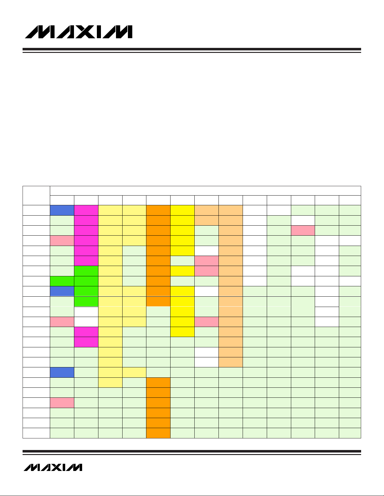
Table 1-1. Register-to-Register Transfer Operations . . . . . . . . . . . . . . . . . . . . . . . . . . . . . . . . . . .1-9
Table 1-2. MAXQ7665/MAXQ7666 Register Modules . . . . . . . . . . . . . . . . . . . . . . . . . . . . . . . . . .1-10
Table 1-3. MAXQ7665A–MAXQ7665D Flash Memory Features . . . . . . . . . . . . . . . . . . . . . . . . . .1-12
Table 1-4. MAXQ7666 Program Flash Features . . . . . . . . . . . . . . . . . . . . . . . . . . . . . . . . . . . . . . .1-12
Table 1-5. MAXQ7666 Data Flash Features . . . . . . . . . . . . . . . . . . . . . . . . . . . . . . . . . . . . . . . . . .1-13
Table 1-6. MAXQ7665/MAXQ7666 Interrupt Sources and Control Bits . . . . . . . . . . . . . . . . . . . . .1-27
Table 1-7. Accumulator Pointer Control Register Settings . . . . . . . . . . . . . . . . . . . . . . . . . . . . . . .1-33
Table 1-8. MAXQ7665/MAXQ7666 System Register Map . . . . . . . . . . . . . . . . . . . . . . . . . . . . . . .1-43
Table 1-9. MAXQ7665/MAXQ7666 System Register Bit Functions and Reset Values . . . . . . . . .1-44
Table 1-10. MAXQ7665/MAXQ7666 Peripheral Register Map . . . . . . . . . . . . . . . . . . . . . . . . . . . .1-62
Table 1-11. MAXQ7665/MAXQ7666 Module 0 Register Bit Functions and Reset Values . . . . . . .1-63
Table 1-12. MAXQ7665/MAXQ7666 Module 1 Register Bit Functions and Reset Values . . . . . . .1-64
Table 1-13. MAXQ7665/MAXQ7666 Module 2 Register Bit Functions and Reset Values . . . . . . .1-65
Table 1-14. MAXQ7665/MAXQ7666 Module 3 Register Bit Functions and Reset Values . . . . . . .1-67
Table 1-15. MAXQ7665/MAXQ7666 Module 4 Register Bit Functions and Reset Values . . . . . . .1-68
Table 1-16. MAXQ7665/MAXQ7666 Module 5 Register Bit Functions and Reset Values . . . . . . .1-70
LIST OF TABLES
LIST OF FIGURES
MAXQ7665/MAXQ7666 User’s Guide
___________________________________________________________________________________________________________ 1-4
Page 7
SECTION 1: MAXQ7665/MAXQ7666 CORE ARCHITECTURE
1.1 Overview
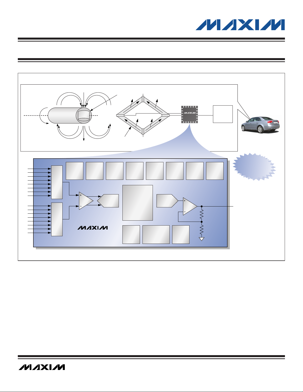
The MAXQ7665/MAXQ7666 are low-power, high-performance, 16-bit RISC microcontrollers based on the MAXQ® architecture. They
include support for integrated, in-system-programmable flash memory and a wide range of peripherals including a 12-bit 500ksps SAR
ADC with a programmable gain amplifier (PGA) and a full CAN 2.0B controller supporting transfer rates up to 1Mbps. The
MAXQ7665/MAXQ7666 are ideally suited for low-cost, low-power embedded applications such as automotive, industrial controls, and
building automation. Except where explicitly noted, the MAXQ7665 and MAXQ7666 features are identical.
The MAXQ7665/MAXQ7666 key features include:
• 8MHz, 16-bit, single-cycle RISC CPU with Harvard Memory Architecture
• Up to 64k x 16 (128kB) on-chip program flash (16kB program flash and dedicated 256B data flash in MAXQ7666) and 512 bytes
internal RAM
• High-precision, low-power analog input/output module including a 12-bit, 500ksps SAR ADC, 1x–32x PGA, 12-bit DAC and
local/remote temperature sensor
• Full CAN 2.0B controller supporting transfer rates up to 1Mbps
• High-performance timer/digital I/O peripherals
• Flexible crystal/clock module
• Advanced power monitoring/management module
1.1.1 References
The online MAXQ7665 and MAXQ7666 QuickView pages contain additional information and links to the data sheet. Errata sheets for the
MAXQ products are available at www
.maxim-ic.com/errata. For more information on other MAXQ microcontrollers, development hard-
ware and software, frequently asked questions and software examples, visit the MAXQ home page at www
.maxim-ic.com/MAXQ. For
general questions and discussion of the MAXQ platform, visit our discussion board at http://discuss.dalsemi.com
.
MAXQ7665/MAXQ7666 User’s Guide
1-5 ___________________________________________________________________________________________________________
MAXQ is a registered trademark of Maxim Integrated Products, Inc.
Figure 1-1. MAXQ7665/MAXQ7666 Block Diagram
PERIPHERAL MODULES
MEMORY MODULE
DATA RAM
256 X 16
(512 BYTES)
PROGRAM FLASH
UP TO 64k X 16
(128kBYTES)
DATA FLASH
256 BYTES
(MAXQ7666 ONLY)
UTILITY ROM
4k X 16
(8kBYTES)
CLOCK/CRYSTAL
MODULE
•
INTERNAL OSCILLATOR
•
HF EXTERNAL XTAL OSC
•
WATCHDOG TIMER
MAXQ7665/MAXQ7666
16-BIT HARVARD
MAXQ20 RISC CPU
•
8MHz OPERATION
•
SINGLE-CYCLE EXECUTION
•
HARVARD ARCHITECTURE
•
INTERRUPT CONTROL
•
16-WORD HW STACK
•
MMU
POWER MANAGEMENT
MODULE
•
POWER-ON RESET
•
I/0 SUPPLY BROWNOUT DETECTOR
•
DIGITAL SUPPLY BROWNOUT DETECTOR
•
+3.3V LINEAR REGULATOR
ANALOG I/0 MODULE
•
8-CHANNEL TRUE-DIFFERENTIAL
MUX
•
PGA 1X, 2X, 4X, 8X, 16X, 32X
•
12-BIT, 500ksps SAR ADC
•
12-BIT VDAC
•
EXT VOLTAGE REF
•
LOCAL TEMP SENSOR
•
REMOTE TEMP SENSOR
TIMER/DIGITAL I/O
PERIPHERALS
•
3 16-BIT TIMER/PWMs
•
1 8-BIT I/O PORT
•
UART AND OPTIONAL SPI
•
CAN INTERFACE
•
JTAG INTERFACE
•
HARDWARE MULTIPLIER
Page 8

1.1.2 Instruction Set
As part of the MAXQ family, the MAXQ7665/MAXQ7666 use the standard 16-bit MAXQ20 instruction set, with all instructions a fixed 16
bits in length. A register-based, transport-triggered architecture allows all instructions to be coded as simple transfer operations. All
instructions reduce to either writing an immediate value to a destination register or memory location or moving data between registers
and/or memory locations.
This simple top-level instruction decoding allows all instructions to be executed in a single cycle. Since all CPU operations are performed on registers only, any new functionality can be added by simply adding new register modules. The simple instruction set also
provides maximum flexibility for code optimization by a compiler.
1.1.3 Harvard Memory Architecture
As part of the MAXQ family, the MAXQ7665/MAXQ7666 core architecture is based on the MAXQ20 design, which implements a 16-bit
internal databus and ALU. Program memory, data memory, and register space on the MAXQ7665/MAXQ7666 follow the Harvard architecture model. Each type of memory is kept separate and is accessed by a separate bus, allowing different word lengths for different
types of memory. Registers may be either 8 or 16 bits in width. Program memory is 16 bits in width to accommodate the standard MAXQ
16-bit instruction set. Data memory is also 16 bits in width but can be accessed in 8-bit or 16-bit modes for maximum flexibility.
The MAXQ7665/MAXQ7666 include a flexible memory management unit (MMU), which allows code to be executed from either the program flash, the utility ROM, or the internal data SRAM. Any of these three memory spaces may also be accessed in data space at any
time, with the single restriction that whichever physical memory area is currently being used as program space cannot be read from
in data space.
1.1.4 Register Space
Since all functions in the MAXQ family are accessed through registers, common functionality is provided through a common register
set. Many of these registers provide the equivalent of higher level op codes by directly accessing the arithmetic logic unit (ALU), the
loop counter registers, and the data pointer registers. Others, such as the interrupt registers, provide common control and configuration functions that are equivalent across all MAXQ microcontrollers.
The common register set, also known as the System Registers, includes the following:
• ALU access and control registers, including working accumulator registers and the processor status flags
• Two Data Pointers and a Frame Pointer for data memory access
• Auto-decrementing Loop Counters for fast, compact looping
• Instruction Pointer and other branching control access points
• Stack Pointer and an access point to the 16-bit-wide dedicated hardware stack
• Interrupt vector, identification, and masking registers
The MAXQ7665/MAXQ7666 peripheral register space (modules 0 to 5) contains registers that access the following peripherals:
• General-purpose, 8-bit, I/O port (P0)
• Serial UART interface
• Serial peripheral interface (SPI)
• Hardware multiplier
• JTAG debug engine
• Three programmable Type 2 timer/counters
• Controller area network (CAN) interface
• Analog input/output module
MAXQ7665/MAXQ7666 User’s Guide
___________________________________________________________________________________________________________ 1-6
Page 9
1.2 Architecture
The MAXQ7665/MAXQ7666 architecture is designed to be modular and expandable. Top-level instruction decoding is extremely simple and based on transfers to and from registers. The registers are organized into functional modules, which are in turn divided into
the system register and peripheral register groups. Figure 1-2 illustrates the modular architecture and the basic transport possibilities.
MAXQ7665/MAXQ7666 User’s Guide
1-7 ___________________________________________________________________________________________________________
Figure 1-2. MAXQ7665/MAXQ7666 Transport-Triggered Architecture
CLOCK CONTROL,
WATCHDOG TIMER
AND POWER MONITOR
CKCN
WDCN
IC
INTERRUPT
LOGIC
IC
IMR
IIR
src
STACK
MEMORY
SP
ADDRESS
GENERATION
IP
LOOP COUNTERS
LC[η]
BOOLEAN
VARIABLE
MANIPULATION
ACCUMULATORS
(16)
AP
APC
PSF
PROGRAM
MEMORY
MEMORY MANAGEMENT
UNIT (MMU)
INSTRUCTION
DECODE
(SRC, DST TRANSPORT
DETERMINATION)
DATA
MEMORY
SC
MUX
SYSTEM MODULES/
REGISTERS
DATA POINTERS
DP[0], DP[1]
FP =
(BP + OFFS)
DPC
dst
dst
src
PERIPHERAL MODULES/REGISTERS
UART
AND SPI
TIMERS/
COUNTERS
GENERAL-
PURPOSE
I/O
CAN
ANALOG
I/0
HARDWARE
MULTIPLIER
JTAG
DEBUG
ENGINE
Page 10

Memory access from the MAXQ7665/MAXQ7666 is based on a Harvard architecture with separate address spaces for program and
data memory. The simple instruction set and transport-triggered architecture allow the MAXQ7665/MAXQ7666 to run in a nonpipelined
execution mode where each instruction can be fetched from memory, decoded, and executed in a single clock cycle. Data memory
is accessed through one of three data pointer registers. Two of these data pointers, DP[0] and DP[1], are stand-alone 16-bit pointers.
The third data pointer, FP, is composed of a 16-bit base pointer (BP) and an 8-bit offset register (OFFS). All three pointers support postincrement/decrement functionality for read operations and pre-increment/decrement for write operations. For the Frame Pointer
(FP=BP[OFFS]), the increment/decrement operation is executed on the OFFS register and does not affect the base pointer (BP). Stack
functionality is provided by dedicated memory with a 16-bit width and depth of 16. An on-chip memory management unit (MMU) is
accessible through system registers to allow logical remapping of physical program and data spaces, and thus facilitates in-system
programming and fast access to data tables, arrays, and constants physically located in program memory.
1.2.1 Instruction Decoding
Every MAXQ7665/MAXQ7666 instruction is encoded as a single 16-bit word according to the format in Figure 1-3.
Bit 15 (f) indicates the format for the source field of the instruction as follows:
• If f equals 0, the instruction is an immediate source instruction, and the source field represents an immediate 8-bit value.
• If f equals 1, the instruction is a register source instruction, and the source field represents the register that the source value will be
read from.
Bits 0 to 7 (ssssssss) represent the source for the transfer. Depending on the value of the format field, this can either be an immediate
value or a source register. If this field represents a register, the lower four bits contain the module specifier and the upper four bits contain the register index in that module.
Bits 8 to 14 (ddddddd) represent the destination for the transfer. This value always represents a destination register, with the lower four
bits containing the module specifier and the upper three bits containing the register subindex within that module.
Since the source field is 8 bits wide and 4 bits are required to specify the module, any one of 16 registers in that module may be specified as a source. However, the destination field has one less bit, which means that only eight registers in a module can be specified
as a destination in a single-cycle instruction.
While the asymmetry between source and destination fields of the op code may initially be considered a limitation, this space can be
used effectively. Firstly, since read-only registers will never be specified as destinations, they can be placed in the second eight locations in a module to give single-cycle read access. Secondly, there are often critical control or configuration bits associated with system and certain peripheral modules where limited write access is beneficial (e.g., watchdog-timer enable and reset bits). By placing
such bits in one of the upper 24 registers of a module, this write protection is added in a way that is virtually transparent to the assembly source code. Anytime that it is necessary to directly select one of the upper 24 registers as a destination, the prefix register PFX is
used to supply the extra destination bits. This prefix register write is inserted automatically by the assembler and requires one additional execution cycle.
The MAXQ7665/MAXQ7666 architecture is transport-triggered. This means that writing to or reading from certain register locations will
also cause side effects to occur. These side effects form the basis for the higher level op codes defined by the assembler, such as
ADDC, OR, JUMP, and so on. While these op codes are actually implemented as MOVE instructions between certain register locations,
the encoding is handled by the assembler and need not be a concern to the programmer. The registers defined in the System Register
and Peripheral Register maps operate as described in the documentation; the unused "empty" locations are the ones used for these
special cases.
The MAXQ7665/MAXQ7666 instruction set is designed to be highly orthogonal. All arithmetic and logical operations that use two registers can use any register along with the accumulator. Data can be transferred between any two registers in a single instruction.
MAXQ7665/MAXQ7666 User’s Guide
___________________________________________________________________________________________________________ 1-8
Figure 1-3. Instruction Word Format
FORMAT DESTINATION SOURCE
f dddddddssssssss
Page 11
1.2.2 Register Space
The MAXQ7665/MAXQ7666 architecture provides a total of 16 register modules. Each of these modules contains 32 registers. Of these
possible 16 register modules, only 13 are used on the MAXQ7665/MAXQ7666—seven for system registers and six for peripheral registers. The first eight registers in each module may be read from or written to in a single cycle; the second eight registers may be read
from in a single cycle and written to in two cycles (by using the prefix register PFX); the last 16 registers may be read or written in two
cycles (always requiring use of the prefix register PFX).
Registers may be either 8 or 16 bits in length. Within a register, any number of bits can be implemented; bits not implemented are fixed
at zero. Data transfers between registers of different sizes are handled as shown in Table 1-1.
• If the source and destination registers are both 8 bits wide, data is transferred bit to bit accordingly.
• If the source register is 8 bits wide and the destination register is 16 bits wide, the data from the source register is transferred
into the lower 8 bits of the destination register. The upper 8 bits of the destination register are set to the current value of the prefix register; this value is normally zero, but it can be set to a different value by the previous instruction if needed. The prefix register reverts back to zero after one cycle, so this must be done by the instruction immediately before the one that will be using
the value.
• If the source register is 16 bits wide and the destination register is 8 bits wide, the lower 8 bits of the source are transferred to
the destination register.
• If both registers are 16 bits wide, data is copied bit to bit.
Table 1-1. Register-to-Register Transfer Operations
The above rules apply to all data movements between defined registers. Data transfer to/from undefined register locations has the following behavior:
• If the destination is an undefined register, the MOVE is a dummy operation but may trigger an underlying operation according
to the source register (e.g., @DP[n]--).
• If the destination is a defined register and the source is undefined, the source data for the transfer will depend upon the source module width. If the source is from a module containing 8-bit or 8-bit and 16-bit source registers, the source data will be equal to the prefix data concatenated with 00h. If the source is from a module containing only 16-bit source registers, 0000h source data is used for
the transfer.
The 16 available register modules are broken up into two different groups. The low six modules (specifiers 0h through 5h) are known
as the Peripheral Register modules, while the high 10 modules (specifiers 6h to Fh) are known as the System Register modules. These
groupings are descriptive only, as there is no difference between accessing the two register groups from a programming perspective.
The System Registers define basic functionality that remains the same across all products based on the MAXQ20 architecture. This
includes all register locations that are used to implement higher level op codes as well as the following common system features.
• ALU (MAXQ20: 16 bits) and associated status flags (zero, equals, carry, sign, overflow)
• 16 working accumulator registers (MAXQ20: 16-bit width), along with associated control registers
• Instruction pointer
• Registers for interrupt control, handling, and identification
• Auto-decrementing loop counters for fast, compact looping
• Two data pointer registers and a frame pointer for data memory access
MAXQ7665/MAXQ7666 User’s Guide
1-9 ___________________________________________________________________________________________________________
SOURCE REGISTER SIZE
(BITS)
88— Source [7:0]
8 16 No 00h Source [7:0]
8 16 Yes Prefix [7:0] Source [7:0]
16 8 — Source [7:0]
16 16 No Source [15:8] Source [7:0]
DESTINATION REGISTER
SIZE (BITS)
PREFIX SET?
DESTINATION SET TO VALUE
HIGH 8 BITS LOW 8 BITS
Page 12
The MAXQ7665/MAXQ7666 peripheral register space (modules 0 to 5) contains registers that access the following peripherals:
• General-purpose, 8-bit, I/O port (P0)
• External interrupts (up to 8)
• Three programmable Type 2 timer/counters
• Serial UART interface
• SPI
• CAN interface
• Analog input/output module
• Hardware multiplier
• JTAG debug engine
The lower 8 bits of all registers in modules 0 to 5 (as well as the AP module M8) are bit addressable.
Table 1-2. MAXQ7665/MAXQ7666 Register Modules
MAXQ7665/MAXQ7666 User’s Guide
__________________________________________________________________________________________________________ 1-10
REGISTER
INDEX
00h PO0 MCNT T2CNA0 T2CNA2 C0C VMC AP A[0] PFX[0] IP
01h MA T2H0 T2H2 C0S APE APC A[1] PFX[1] SP
02h MB T2RH0 T2RH2 C0IR ACNT A[2] PFX[2] IV
03h EIF0 MC2 T2CH0 T2CH2 C0TE DCNT A[3] PFX[3] OFFS DP0
04h MC1 T2CNA1 C0RE DACI PSF A[4] PFX[4] DPC
05h MC0 T2H1 COR IC A[5] PFX[5] GR
06h SPIB T2RH1 C0DP DACO IMR A[6] PFX[6] LC0 GRL
07h SBUF0 SPICN T2CH1 C0DB A[7] PFX[7] LC1 BP DP1
08h PI0 SPICF T2CNB0 T2CNB2 C0RMS ADCD SC A[8] GRS
09h SPICK T2V0 T2V2 C0TMA TSO A[9] GRH
0Ah FCNTL T2R0 T2R2 AIE A[10] GRXL
0Bh EIE0 FDATA T2C0 T2C2 ASR IIR A[11] FP
0Ch MC1R T2CNB1 OSCC A[12]
0Dh MC0R T2V1 A[13]
0Eh T2R1 CKCN A[14]
0Fh T2C1 WDCN A[15]
10h PD0 T2CFG0 T2CFG2
11h T2CFG1 C0M1C
12h C0M2C
13h EIES0 C0M3C
14h C0M4C
15h C0M5C
16h C0M6C
M0 M1 M2 M3 M4 M5 M8 M9 M11 M12 M13 M14 M15
MODULE NAME (BASE SPECIFIER)
Page 13
1.2.3 Memory Organization
Beyond the internal register space, memory on the MAXQ7665/MAXQ7666 microcontrollers is organized according to a Harvard architecture, with a separate address space and bus for program memory and data memory. Stack memory is also separate and is
accessed through a dedicated register set.
To provide additional memory map flexibility, an MMU allows data memory space to be mapped into a predefined program memory
segment, thus affording the possibility of code execution from data memory. Additionally, program memory space can be made accessible as data space, allowing access to constant data stored in program memory. All memory is internal, and physical memory segments (other than the stack and register memories) can be accessed as either program memory or as data memory, but not both at
once.
1.2.3.1 Program Memory
The MAXQ7665/MAXQ7666 contain up to 64k x 16 (128kB) of flash memory, which normally serves as program memory. When executing from the data SRAM or utility ROM, this memory is mapped to data space and can be used for lookup tables and similar functions. Flash memory mapped into data space can be read from directly, like any other type of data memory. However, writing to flash
memory must be done by calling the in-application functions provided by the utility ROM. The utility ROM provides routines to carry
out the necessary operations (erase, write) on flash memory.
Table 1-3 summarizes the features of the flash memory supported in the MAXQ7665A–MAXQ7665D devices. The MAXQ7666 device
features a 256B data flash in addition to 16kB program flash. The MAXQ7666 flash is different from the MAXQ7665A–MAXQ7665D and
its features are summarized in Tables 1-4 and 1-5. Refer to the respective data sheets for additional information.
Program memory begins at address 0000h and is contiguous through the internal program memory. The actual size of the on-chip program memory available for user application is product dependent. Given a 16-bit program address bus, the maximum program space
is 64kWords. Since the codewords are 16 bits, the program memory is, therefore, a 64k x 16 linear space.
MAXQ7665/MAXQ7666 User’s Guide
1-11 __________________________________________________________________________________________________________
Table 1-2. MAXQ7665/MAXQ7666 Register Modules (continued)
REGISTER
INDEX
M0 M1 M2 M3 M4 M5 M8 M9
MODULE NAME (BASE SPECIFIER)
M11 M12 M13 M14 M15
17h C0M7C
18h ICDT0 C0M8C
19h ICDT1 C0M9C
1Ah ICDC C0M10C
1Bh ICDF C0M11C
1Ch FADDR ICDB C0M12C
1Dh SCON0 ICDA C0M13C
1Eh SMD0 ICD D C0M14C
1Fh PR0 C0M15C
RESERVED
OR
OPCO DE
PORT
PINS
(GPIO)
SERIAL
AND
SPI
INTERRUPT
CON TROL
HARDWARE
MULTIPLIER
TIMERS CAN
ANALOG
I/O
AC C ARRAY,
CON TROL
OTHER
FUNCTIONS
Page 14
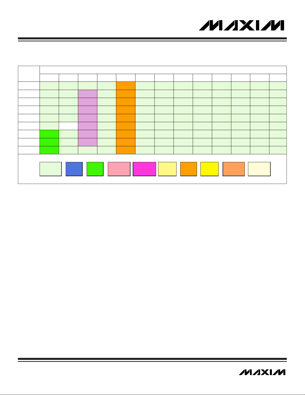
Table 1-3. MAXQ7665A–MAXQ7665D Flash Memory Features
MAXQ7665/MAXQ7666 User’s Guide
__________________________________________________________________________________________________________ 1-12
Table 1-4. MAXQ7666 Program Flash Features
FEA TURE MAXQ7665A MAXQ7665B MAXQ7665C MAXQ7665D
Flash Type Type A Type A Type A Type A
Flash Siz e 128kB (64k x 16) 64kB (32k x 16) 48kB (24k x 16) 32kB (16k x 16)
Flash Organization 5 Sectors 4 Sectors 3 Sectors 3 Sectors
0000h–7FFFh
(32k x 16)
8000h–BFFFh
(16k x 16)
Sector Address/Size
Flash Erase
Flash Program Word Write Word Write Word Write Word Write
In Application Programming Yes, using utility ROM routines. See Section 15 for more infor mation.
In System Programming Yes, using utility ROM JTAG bootstrap loader. See Section 12 for more i nfor mation.
C000h–DFFFh
(8k x 16)
E000h–EFFFh
(4k x 16)
F000h–FFFFh
(4k x 16)
Erase All Erase All Erase All Erase All
Sector Erase Sector Erase Sector Erase Sector Erase
0000h–3FFFh
(16k x 16)
4000h–5FFFh
(8k x 16)
6000h–6FFFh
(4k x 16)
7000h–7FFFh
(4k x 16)
— — —
0000h–3FFFh
(16k x 16)
4000h–4FFFh
(4k x 16)
5000h–5FFFh
(4k x 16)
— —
0000h–1FFFh
(8k x 16)
2000h–2FFFh
(4k x 16)
3000h–3FFFh
(4k x 16)
FEA TURE MAXQ7666
Flash Type Type F
Progra m Flash Size 16kB (8k x 16)
Program Flash Organization
Program Flash Page Address
Program Flash Erase
Program Flash Write 1 Page Write
In App l ication Progra mming Yes, using utility RO M routines . See Section 16 for more information.
In System Programming Yes, using utility ROM JTAG bootstrap loader. See Section 12 for more information.
256 Pages
1 Page = 64B (32 x 16)
0000h–001Fh (Page 0)
0020h–003Fh (Page 1)
0040h–005Fh (Page 2)
. . .
1FC0h–1FDFh (Page 254)
1FE0h–1FFFh (Page 255)
Erase All
2 Page E rase
Page 15

MAXQ7665/MAXQ7666 User’s Guide
1-13 __________________________________________________________________________________________________________
Table 1-5. MAXQ7666 Data Flash Features
Program memory is accessed directly by the program fetching unit and is addressed by the Instruction Pointer register. From an implementation perspective, system interrupts and branching instructions simply change the contents of the Instruction Pointer and force
the op code fetch from a new program location. The Instruction Pointer is direct read/write accessible by the user software; write access
to the Instruction Pointer will force program flow to the new address on the next cycle following the write. The contents of the Instruction
Pointer will be incremented by 1 automatically after each fetch operation. The Instruction Pointer defaults to 8000h, which is the starting address of the utility ROM. The default IP setting of 8000h is assigned to allow initial in-system programming to be accomplished
with utility ROM code assistance. The utility ROM code interrogates a specific register bit in order to decide whether to execute in-system programming or jump immediately to user code starting at 0000h. The user code reset vector should always be stored in the lowest bytes of the program memory.
FEA TURE MAXQ7666
Flash Type Type F
Data Flash Size 256B (128 x 16)
Data Flash Organization (Regular Mode)
Data Flash Page Address (Regular Mode)
Data Flash Erase
(Regular Mode)
Data Flash Wr ite
(Regular Mode)
Data Flash Organization
(Even Mode)
Data Flash Page Address ( Ev en Mode)
Data Flash Erase
(Even Mode)
Data Flash Wr ite
(Even Mode)
In App l ication Progra mming Yes, using utility RO M routines . See Section 16 for more information.
In System Programming Not supported, only in application programming.
128 Pages
1 Page = 2B (1 x 16)
4000h (Page 0)
4001h (Page 1)
4002h (Page 2)
….
407Fh (Page 127)
Erase All
2 Page E rase
1 Page Write
64 Even Pages
1 Page = 2B (1 x 16)
4000h (Page 0)
4002h (Page 1)
4004h (Page 2)
. . .
407Eh (Page 63)
Erase All
1 Page E rase
1 Page Write
Page 16

1.2.3.2 Utility ROM
A utility ROM (4k x 16) is placed in the upper 32kWord program memory space starting at address 8000h. This utility ROM provides
the following system utility functions:
• Reset vector
• Bootstrap function for system initialization
• In-application programming
• In-circuit debug
Following each reset, the processor automatically starts execution at address 8000h in the utility ROM, allowing ROM code to perform
any necessary system support functions. Next, the System Programming Enable (SPE) bit is examined to determine whether system
programming should commence or whether that code should be bypassed, instead forcing execution to vector to the start of user program code. When the SPE bit is set to logic 1, the processor will execute the prescribed Bootstrap Loader mode program that resides
in utility ROM. The SPE bit defaults to 0. To enter the Bootstrap Loader mode, the SPE bit can be set to 1 during reset via the JTAG
interface. When in-system programming is complete, the Bootstrap Loader can clear the SPE bit and reset the device such that the insystem programming routine is subsequently bypassed.
The MAXQ7665/MAXQ7666 application programming routines available as part of the utility ROM are covered in Sections 15 and 16.
The MAXQ7665/MAXQ7666 JTAG test access port, in-circuit debug, and bootstrap loader mode for in-system programming are covered in Sections 10, 11, and 12.
1.2.3.3 Data Memory
The MAXQ7665/MAXQ7666 contain 256 x 16 (512 bytes) of on-chip data SRAM that can be mapped into either program or data space.
The contents of this SRAM are indeterminate after power-on reset, but are maintained during stop mode and across non-POR resets,
as long as the DVDD supply stays within the acceptable range.
On-chip data memory begins at address 0000h and is contiguous through the internal data memory. Data memory is accessed via
indirect register addressing through a Data Pointer (@DP[n]) or Frame Pointer (@BP[OFFS]). The Data Pointer is used as one of the
operands in a MOVE instruction. If the Data Pointer is used as source, the core performs a Load operation that reads data from the
data memory location addressed by the Data Pointer. If the Data Pointer is used as destination, the core executes a Store operation
that writes data to the data memory location addressed by the Data Pointer. The Data Pointer can be directly accessed by the user
software.
The core incorporates two 16-bit Data Pointers (DP[0] and DP[1]) to support data memory accessing. All Data Pointers support indirect addressing mode and indirect addressing with auto-increment or auto-decrement. Data Pointers DP[0] and DP[1] can be used as
post increment/decrement source pointers by a MOVE instruction or pre increment/decrement destination pointers by a MOVE instruction. Using Data Pointer indirectly with "++" will automatically increase the content of the active Data Pointer by 1 immediately following the execution of read data transfer (@DP[n]++) or immediately preceding the execution of a write operation (@++DP[n]). Using
Data Pointer indirectly with "--" will decrease the content of the active Data Pointer by 1 immediately following the execution of read
data transfer (@DP[n]--) or immediately preceding the execution of a write operation (@--DP[n]).
The Frame Pointer (BP[OFFS]) is formed by 16-bit unsigned addition of Frame Pointer Base Register (BP) and Frame Pointer Offset
Register (OFFS). Frame Pointer can be used as a post increment/decrement source pointer by a MOVE instruction or as a pre increment/decrement destination pointer. Using Frame Pointer indirectly with "++" (@BP[++OFFS] for a write or @BP[OFFS++] for a read) will
automatically increase the content of the Frame Pointer Offset by 1 immediately before or after the execution of data transfer depending
upon whether it is used as a destination or source pointer respectively. Using Frame Pointer indirectly with "--" (@BP[--OFFS] for a write or
@BP[OFFS--] for a read) will decrease the content of the Frame Pointer Offset by 1 immediately before/after execution of data transfer
depending upon whether it is used as a destination or source pointer respectively. Note that the increment/decrement function affects the
content of the OFFS register only, while the contents of the BP register remain unaffected by the borrow/carry out from the OFFS register.
A data memory cycle contains only one system clock period to support fast internal execution. This allows read or write operations on
SRAM to be completed in one clock cycle. Data memory mapping and access control are handled by the MMU. Read/write access to
the data memory can be in word or in byte.
When using the in-circuit debugging features of the MAXQ7665/MAXQ7666, the top 19 bytes (bytes 0x1ED to 0x1FF) of the SRAM must
be reserved for saved state storage and working space for the debugging routines in the utility ROM. If in-circuit debug will not be
used, the entire SRAM is available for application use.
MAXQ7665/MAXQ7666 User’s Guide
__________________________________________________________________________________________________________ 1-14
Page 17

1.2.3.4 Stack Memory
The MAXQ7665/MAXQ7666 provide a 16 x 16 hardware stack to support subroutine calls and system interrupts. A 16-bit wide on-chip
stack is provided by the MAXQ7665/MAXQ7666 for storage of program return addresses and general-purpose use. The stack is used
automatically by the processor when the CALL, RET, and RETI instructions are executed and when an interrupt is serviced; it can also
be used explicitly to store and retrieve data by using the @SP- - source, @++SP destination, or the PUSH, POP, and POPI instructions.
The POPI instruction acts identically to the POP instruction except that it additionally clears the INS bit.
The width of the stack is 16 bits to accommodate the instruction pointer size. The stack depth is 16 for the MAXQ7665/MAXQ7666. As
the stack pointer register SP is used to hold the index of the top of the stack, the maximum size of the stack allowed is defined by the
number of bits defined in the SP register (e.g., 4 bits for stack depth of 16).
On reset, the stack pointer SP initializes to the top of the stack (e.g. 0Fh for a 16-word stack). The CALL, PUSH, and interrupt vectoring operations increment SP and then store a value at @SP. The RET, RETI, POP, and POPI operations retrieve the value at @SP and
then decrement SP.
As with the other RAM-based modules, the stack memory is initialized to indeterminate values upon reset or power-up. Stack memory
is dedicated for stack operations only and cannot be accessed through program or data address spaces.
When using the in-circuit debugging features of the MAXQ7665/MAXQ7666, one word of the stack must be reserved to store the return
location when execution branches into the debugging routines in the utility ROM. If in-circuit debug will not be used, the entire stack
is available for application use.
1.2.3.5 Pseudo-Von Neumann Memory Mapping
The MAXQ7665/MAXQ7666 support a pseudo-Von Neumann memory structure that can merge program and data into a linear memory map. This is accomplished by mapping the data memory into the program space or mapping program memory segment into the
data space. Program memory from 0000h to 7FFFh is the normal user code segment, followed by the utility ROM segment. The uppermost part of the 64kWord memory is the logical area for data memory when accessed as a code segment.
The program memory is logically divided into four program pages:
• P0 contains the lower 16kWords,
• P1 contains the second 16kWords,
• P2 contains the third 16kWords, and
• P3 contains the fourth 16kWords.
By default, P2 and P3 are not accessible for program execution until they are explicitly activated by the user software. The Upper
Program Access (UPA) bit must be set to logic 1 to activate P2 and P3. Once UPA is set, P2 and P3 will occupy the upper half of the
64kWord program space. In this configuration (UPA = 1), the utility ROM cannot be accessed as program memory and the physical
data memory cannot be accessed logically in program space.
The logical mapping of physical program memory page(s) into data space depends upon two factors: physical memory currently in
use for program execution; and word/byte data memory access selection. If execution is from the utility ROM, physical program memory page(s) can logically be mapped to the upper half of data memory space. If logical data memory is used for execution, physical
program memory page(s) can logically be mapped to the lower half of data memory space. If byte access mode is selected, only one
page (16kWords) may be logically mapped, as just defined, to either the upper or lower half of data memory. If word access mode is
selected, two pages (32kWords total) may be logically mapped to data memory. To avoid memory overlapping in the byte access
mode, the physical data memory should be confined to the address range 0000h to 3FFFh in word mode. The selection of physical
memory page or pages to be logically mapped to data space is determined by the Code Access Bits (CDA1:0):
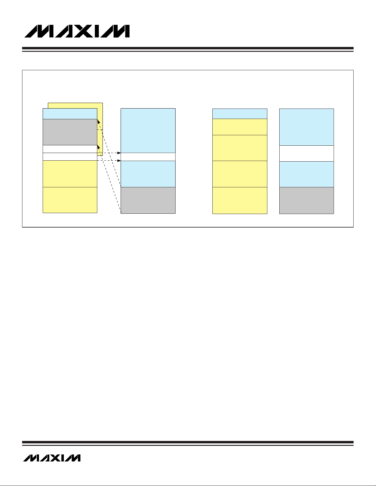
Figure 1-4 summarizes the default memory maps for this memory structure. The primary difference lies in the reset default settings for
the data pointer Word/Byte Mode Select (WBSn) bits. The WBSn bits of the MAXQ7665/MAXQ7666 default to word access mode
(WBSn = 1).
MAXQ7665/MAXQ7666 User’s Guide
1-15 __________________________________________________________________________________________________________
CDA1:0 SELECTED PAGE IN BYTE MODE
00 P0 P0 and P1
01 P1 P0 and P1
10 P2 P2 and P3
11 P3 P2 and P3
SELECTED PAGE IN
WORD MODE
Page 18
1.2.3.6 Pseudo-Von Neumann Memory Access
The pseudo-Von Neumann memory mapping is straightforward if there is no memory overlapping among the program, utility ROM, and
data memory segments. However, for applications requiring large-size program memory, the paging scheme can be used to selectively
activate those overlapped memory segments. The UPA bit can be used to activate the upper half of the physical program code (P2 and
P3) for program execution. When accessing the program memory as data, the CDA bits can be used to select one of the four program
pages as needed. Full data memory access to any of the four physical program memory pages is based on the assumption that the maximum physical data memory is in the range of 16k x 16. The other restriction for accessing the pseudo-Von Neumann map is that when
program execution is in a particular memory segment, the same memory segment cannot be simultaneously be accessed as data.
When executing from the lower 32k program space (P0 and P1):
• The upper half of the code segment (P2 and P3) is accessible as program if the UPA bit is set to 1.
• The physical data memory is available for accessing as a code segment with offset at A000h if the UPA bit is 0.
• Load and Store operations addressed to physical data memory are executed as normal.
• The utility ROM can be read as data, starting at 8000h of the data space.
When executing from the utility ROM (only allowable when UPA = 0):
• The lower 32k program space (P0 and P1) functions as normal program memory.
• The upper half of the code segment (P2 and P3) is not accessible as program (since UPA = 0).
• The physical data memory is available for accessing as a code segment with offset at A000h.
• Load and Store operations addressed to physical data memory are executed as normal.
• One page (byte access mode) or two pages (word access mode) can be accessed as data with offset at 8000h as determined
by the CDA1:0 bits.
When executing from the data memory (only allowable when UPA = 0):
• Program flows freely between the lower 32k user code (P0 and P1) and the utility ROM segment.
• The upper half of the code segment (P2 and P3) is not accessible as program (since UPA = 0).
MAXQ7665/MAXQ7666 User’s Guide
__________________________________________________________________________________________________________ 1-16
Figure 1-4. Pseudo-Von Neumann Memory Map (MAXQ7665/MAXQ7666 Default)
MAXQ7665/MAXQ7666 MEMORY MAP (DEFAULT CONDITION, UPA = 0)
PROGRAM MEMORY
15 0
FFFFh
A100h
A000h
9000h
8000h
0000h
LOGICAL SPACE
Physical Program
LOGICAL SPACE
UTILITY ROM
PHYSICAL PROGRAM
(P1)
PHYSICAL PROGRAM
(P0)
P3
(P0)
P2
DATA MEMORY
15
LOGICAL SPACE
PHYSICAL DATA
0
FFFFh
9000h
8000h
0100h
0000h
MAXQ7665/MAXQ7666 MEMORY MAP (UPA = 1, CDA IS DON’T CARE)
DATA MEMORYPROGRAM MEMORY
FFFFh
8000h
0000h
15
LOGICAL SPACE
PHYSICAL PROGRAM
(P3)
PHYSICAL PROGRAM
(P2)
PHYSICAL PROGRAM
(P1)
PHYSICAL PROGRAM
(P0)
0
15
LOGICAL UTILITY ROM
LOGICAL SPACE
PHYSICAL DATA
0
FFFFh
9000h
8000h
0100h
0000h
Page 19

• The utility ROM can be accessed as data with offset at 8000h.
• One page (byte access mode) or two pages (word access mode) can be accessed as data with offset at 0000h as determined
by the CDA1:0 bits.
1.2.3.7 Data Alignment
To support merged program and data memory operation while maintaining efficiency on memory space usage, the data memory must
be able to support both byte-wide and word-wide accessing. Data is aligned in data memory as word, but the effective data address is
resolved to bytes. This data alignment allows direct program fetching in its native word size while maintaining accessibility at the byte
level. It is important to realize that this accessibility requires strict word alignment. All executable words must align to an even address
in byte mode. Care must be taken when updating the code segment in the unified data memory space as misalignment of words will
likely result in loss of program execution control. Worst yet, this situation may not be detected if the watchdog timer is also disabled.
Data memory is organized as two byte-wide memory banks with common word address decode but two 8-bit data buses. The data
memory will always be read as a complete word, independent of operation, whether program fetch or data access. The program
decoder always uses the full 16-bit word, whereas the data access can utilize a word or an individual byte.
In byte mode, data pointer hardware reads out the word containing the selected byte using the effective data word address pointer
(the least significant bit of the byte data pointer is not initially used). Then, the least significant data pointer bit functions as the byte
select that is used to place the target byte to the data path. For write access, data pointer hardware addresses a particular word using
the effective data word address while the least significant bit selects the corresponding data bank for write, leaving the contents of the
other memory bank unaffected.
1.2.3.8 Memory Management Unit
Memory allocation and accessing control for program and data memory can be managed by the memory management unit (MMU). A
single memory management unit option is discussed in this user’s guide, however the memory management unit implementation for
any given product depends upon the type and amount of memory addressable by the device. Users should consult the individual product data sheet(s) and/or user’s guide supplement(s) for detailed information.
Although supporting less than the maximum addressable program and data memory segments, the MMU implementation presented
provides a high degree of programming and access control flexibility. It supports the following:
• User program memory up to 32k x 16 (up to 64k x 16 with inclusion of UPA bit).
• Utility ROM up to 8k x 16.
• Data memory SRAM up to 16k x 16.
• In-system and in-application programming of embedded EEPROM, flash, or SRAM memories.
• Access to any of the three memory areas (SRAM, code memory, utility ROM) using the data memory pointers.
• Execution from any of the three memory areas (SRAM, code memory, factory written and tested utility-ROM routines).
Given these capabilities, the following rules apply to the memory map:
• A particular memory segment cannot be simultaneously accessed as both program and data.
• The offset address is A000h when logically mapping data memory into the program space.
• The offset for logically mapping the utility ROM into the data memory space is 8000h.
• Program memory:
- The lower half of the program memory (P0 and P1) is always accessible, starting at 0000h.
- The upper half of the program memory (P2 and P3) must be activated by setting the UPA bit to 1 when accessing for code
execution, starting at 8000h.
- Setting the UPA bit to 1 disallows access to the utility ROM and logical data memory as program.
- Physical program memory pages (P0, P1, P2, P3) are logically mapped into data space based upon the memory segment
currently being used for execution, selection of byte/word access mode, and CDA1:0 bit settings (described in the
Pseudo-
Von Neumann Memory Map
and
Pseudo-Von Neumann Memory Access
sections).
• Data memory
- Access can be either word or byte.
- All 16 data pointer address bits are significant in either access mode (word or byte).
MAXQ7665/MAXQ7666 User’s Guide
1-17 __________________________________________________________________________________________________________
Page 20
MAXQ7665/MAXQ7666 User’s Guide
__________________________________________________________________________________________________________ 1-18
Figure 1-5. CDA Functions (Word Access Mode)
MAXQ7665/MAXQ7666 MEMORY MAP (UPA = 0, EXECUTING FROM UTILITY ROM)
PROGRAM MEMORY
15 0
FFFFh
A100h
A000h
9000h
8000h
0000h
LOGICAL SPACE
LOGICAL DATA
LOGICAL SPACE
UTILITY ROM
PHYSICAL PROGRAM
(P1)
PHYSICAL PROGRAM
(P0)
15
P3
P2
CDA1 = 1
CDA1 = 0
DATA MEMORY
PHYSICAL DATA
MAXQ7665/MAXQ7666 MEMORY MAP (UPA = 0, EXECUTING FROM LOGICAL DATA MEMORY)
DATA MEMORYPROGRAM MEMORY
15 0
FFFFh
A100h
A000h
9000h
8000h
LOGICAL SPACE
LOGICAL DATA MEMORY
LOGICAL SPACE
UTILITY ROM
P3
P2
15
LOGICAL SPACE
LOGICAL UTILITY ROM
0
0
8000h
0100h
0000h
FFFFh
8000h
PHYSICAL PROGRAM
PHYSICAL PROGRAM
0000h
(P1)
(P0)
CDA1 = 0
CDA1 = 1
0000h
Page 21
MAXQ7665/MAXQ7666 User’s Guide
1-19 __________________________________________________________________________________________________________
Figure 1-6. CDA Functions (Byte Access Mode)
EXECUTING FROM UTILITY ROM (UPA = 0, ONLY P1, P2 PRESENT)
15 0 07
FFFFh
A100h
A000h
9000h
8000h
LOGICAL SPACE
LOGICAL DATA
MEMORY
LOGICAL SPACE
UTILITY ROM
PHYSICAL PROGRAM
(P1)
CDA0 = 1
DATA MEMORYPROGRAM MEMORY
FFFFh
8000h
LOGICAL SPACE
0200h
CDA0 = 0
0000h
PHYSICAL PROGRAM
(P0)
EXECUTING FROM LOGICAL DATA MEMORY (UPA = 0, ONLY P1, P2 PRESENT)
15 0
FFFFh
A100h
A000h
9000h
8000h
0000h
LOGICAL SPACE
LOGICAL DATA
MEMORY
LOGICAL SPACE
UTILITY ROM
PHYSICAL PROGRAM
(P1)
PHYSICAL PROGRAM
(P0)
CDA0 = 1
CDA0 = 0
PHYSICAL DATA
DATA MEMORYPROGRAM MEMORY
LOGICAL SPACE
07
0000h
FFFFh
8000h
0000h
Page 22

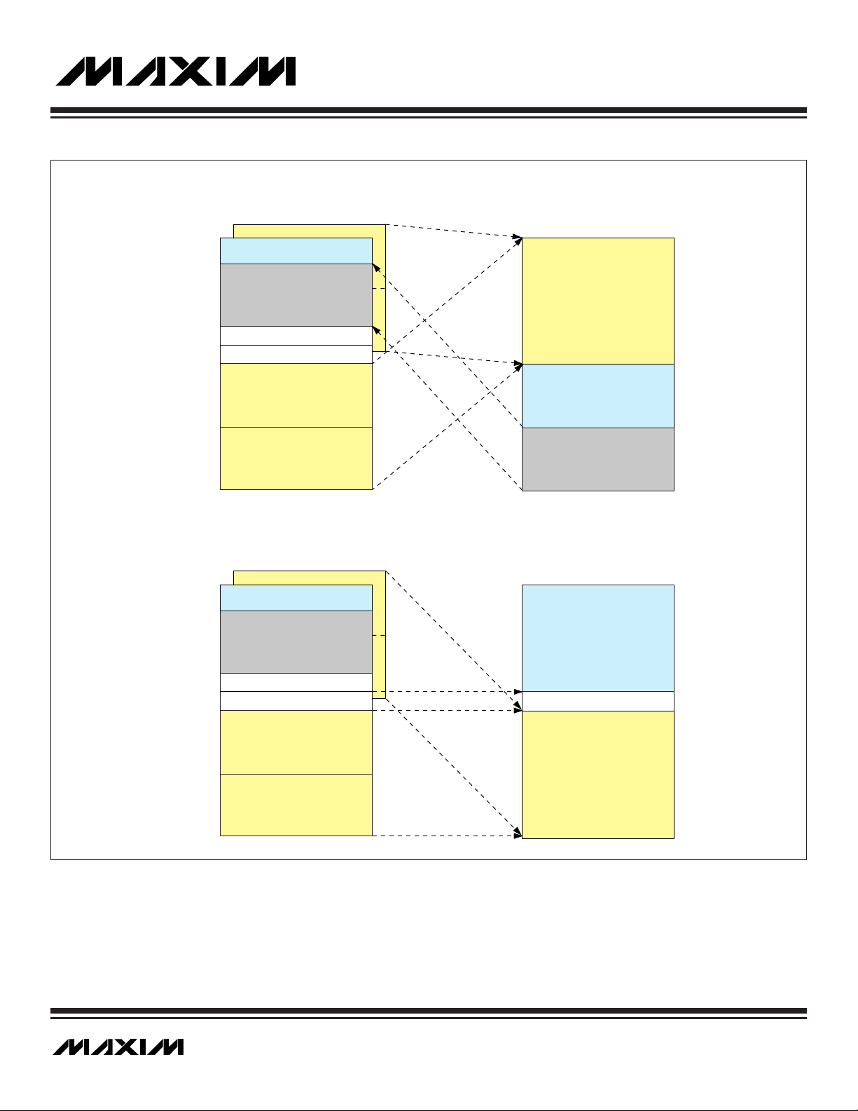
1.2.3.9 Program and Data Memory Mapping Example 1: MAXQ7665B
Figures 1-7, 1-8, and 1-9 show the mapping of physical memory segments into the program and data memory space for the
MAXQ7665B with 32k x 16 (64kB) program flash memory. In this case and all cases when program flash memory size is ≤ 32k x 16,
the memory mapping is straightforward as there is no overlapping among the program, utility ROM, and data memory segments. The
mapping of memory segments into program space is always the same. The mapping of memory segments into data space varies
depending on which memory segment is currently being executed from.
In all cases, whichever memory segment is currently being executed from in program space cannot be accessed in data space.
MAXQ7665/MAXQ7666 User’s Guide
__________________________________________________________________________________________________________ 1-20
Figure 1-7. MAXQ7665B Memory Map When Executing from Application Flash
PROGRAM
SPACE
256 x 16
DATA SRAM
4k x 16
UTILITY ROM
32k x 16
PROGRAM FLASH
A0FFh
A000h
8FFFh
8000h
7FFFh
EXECUTING FROM
0000h
DATA SPACE
(BYTE MODE)
8k x 8
UTILITY ROM
512 x 8
DATA SRAM
9FFFh
8000h
01FFh
0000h
DATA SPACE
(WORD MODE)
4k x 16
UTILITY ROM
256 x 16
DATA SRAM
8FFFh
8000h
00FFh
0000h
Page 23
MAXQ7665/MAXQ7666 User’s Guide
1-21 __________________________________________________________________________________________________________
Figure 1-9. MAXQ7665B Memory Map When Executing from Data SRAM
Figure 1-8. MAXQ7665B Memory Map When Executing from Utility ROM
PROGRAM
SPACE
256 x 16
DATA SRAM
4k x 16
UTILITY ROM
EXECUTING FROM
32k x 16
PROGRAM FLASH
A0FFh
A000h
8FFFh
8000h
7FFFh
0000h
DATA SPACE
(BYTE MODE)
32k x 8
PROGRAM FLASH
PAGE 0
(IF CDA0 = 0)
PAGE 1
(IF CDA0 = 1)
512 x 8
DATA SRAM
FFFFh
8000h
01FFh
0000h
DATA SPACE
(WORD MODE)
32k x 16
PROGRAM FLASH
PAGES 0 AND 1
256 x 16
DATA SRAM
FFFFh
8000h
00FFh
0000h
PROGRAM
SPACE
256 x 16
DATA SRAM
A0FFh
A000h
EXECUTING FROM
87FFh
4k x 16
UTILITY ROM
8000h
7FFFh
32k x 16
PROGRAM FLASH
0000h
DATA SPACE
(BYTE MODE)
8k x 8
UTILITY ROM
32k x 8
PROGRAM FLASH
PAGE 0
(IF CDA0 = 0)
PAGE 1
(IF CDA0 = 1)
9FFFh
8000h
7FFFh
0000h
DATA SPACE
(WORD MODE)
8FFFh
4k x 16
UTILITY ROM
8000h
7FFFh
32k x 16
PROGRAM FLASH
PAGES 0 AND 1
0000h
Page 24
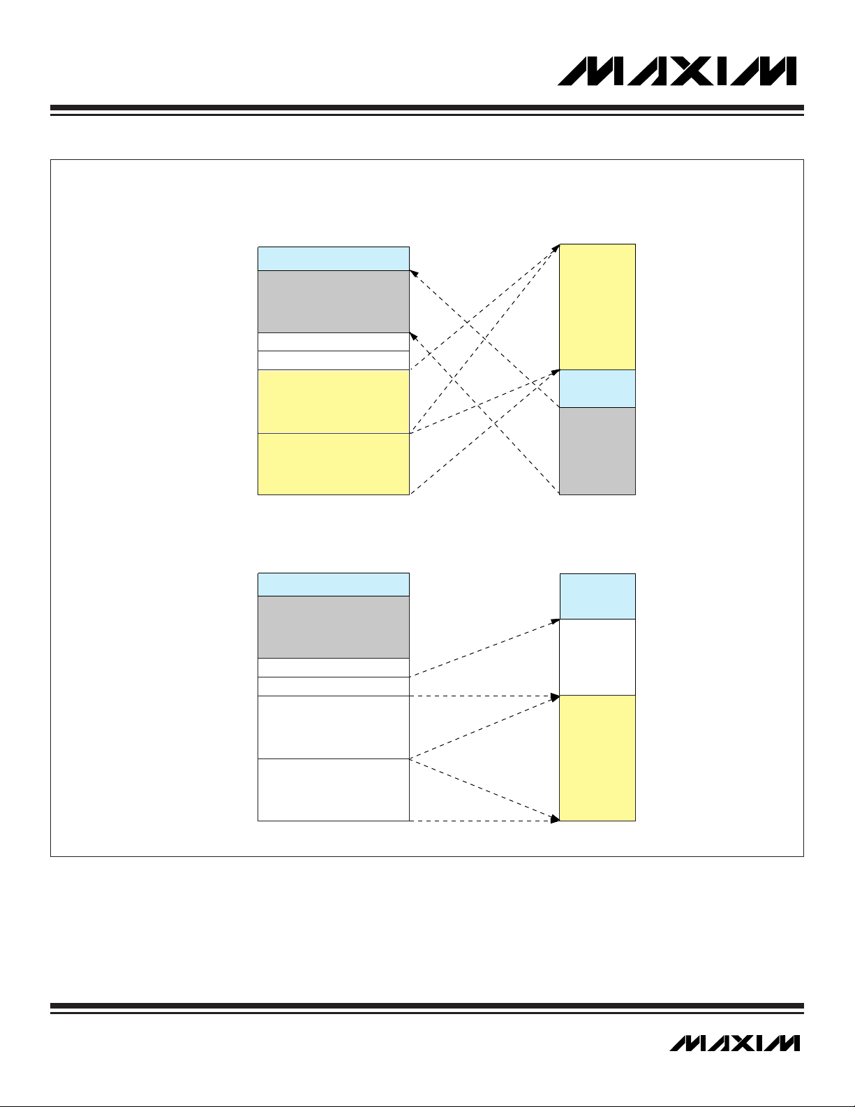
1.2.3.10 Program and Data Memory Mapping Example 2: MAXQ7666
Figures 1-10, 1-11, and 1-12 show the mapping of physical memory segments into the program and data memory space for the
MAXQ7666 with 8k x 16 (16kB) program flash memory, 256B data flash memory, and 512B data RAM.
MAXQ7665/MAXQ7666 User’s Guide
__________________________________________________________________________________________________________ 1-22
Figure 1-10. MAXQ7666 Memory Map When Executing from Application Flash
Figure 1-11. MAXQ7666 Memory Map When Executing from Utility ROM
PROGRAM
SPACE
A0FFh
A000h
8FFFh
8000h
407Fh
4000h
1FFFh
0000h
EXECUTING FROM
256 x 16
DATA RAM
4k x 16
4k x 16
UTILITY ROM
UTILITY ROM
128 x 16
DATA FLASH
8k x 16
PROGRAM FLASH
PROGRAM
SPACE
DATA SPACE
(BYTE MODE)
8k x 8
UTILITY ROM
512 x 8
DATA RAM
DATA SPACE
(BYTE MODE)
9FFFh
8000h
01FFh
0000h
DATA SPACE
(WORD MODE)
4k x 16
UTILITY ROM
256 x 16
DATA RAM
DATA SPACE
(WORD MODE)
8FFFh
8000h
00FFh
0000h
A0FFh
A000h
8FFFh
8000h
407Fh
4000h
1FFFh
0000h
EXECUTING FROM
256 x 16
DATA SRAM
4k x 16
4k x 16
UTILITY ROM
UTILITY ROM
128 x 16
DATA FLASH
8k x 16
PROGRAM FLASH
256 x 8
DATA FLASH
(CDA0 =1)
16k x 8
PROGRAM FLASH
(CDA0 = 0)
512 x 8
DATA RAM
80FFh
8000h
BFFFh
8000h
01FFh
0000h
128 x 16
DATA FLASH
8k x 16
PROGRAM FLASH
256 x 16
DATA RAM
C07Fh
C000h
9FFFh
8000h
00FFh
0000h
Page 25
MAXQ7665/MAXQ7666 User’s Guide
1-23 __________________________________________________________________________________________________________
Figure 1-12. MAXQ7666 Memory Map When Executing from Data RAM
1.2.4 Interrupts
The MAXQ7665/MAXQ7666 provide a single, programmable interrupt vector (IV) that can be used to handle internal and external interrupts. Interrupts can be generated from system level sources (e.g., watchdog timer) or by sources associated with the peripheral modules included in the specific MAXQ7665/MAXQ7666 microcontrollers. Only one interrupt can be handled at a time, and all interrupts
naturally have the same priority. A programmable interrupt mask register allows software-controlled prioritization and nesting of highpriority interrupts.
1.2.4.1 Servicing Interrupts
For the MAXQ7665/MAXQ7666 to service an interrupt, interrupts must be enabled globally, modularly, and locally. The Interrupt Global
Enable (IGE) bit located in the Interrupt Control (IC) register acts as a global interrupt mask. This bit defaults to 0, and it must be set
to 1 before any interrupt takes place.
The local interrupt-enable bit for a particular source is in one of the peripheral registers associated with that peripheral module, or in a
system register for any system interrupt source. Between the global and local enables are intermediate per-module and system interrupt
mask bits. These mask bits reside in the Interrupt Mask system register. By implementing intermediate per-module masking capability in
a single register, interrupt sources spanning multiple modules can be selectively enabled/disabled in a single instruction. This promotes
a simple, fast, and user-definable interrupt prioritization scheme. The interrupt source-enable hierarchy is illustrated in Figure 1-13.
When an interrupt condition occurs, its individual flag is set, even if the interrupt source is disabled at the local, module, or global level.
Interrupt flags must be cleared within the user interrupt routine to avoid repeated interrupts from the same source.
Since all interrupts vector to the address contained in the Interrupt Vector (IV) register, the Interrupt Identification Register (IIR) may be
used by the interrupt service routine to determine the module source of an interrupt. The IIR contains a bit flag for each peripheral module and one flag associated with all system interrupts; if the bit for a module is set, then an interrupt is pending that was initiated by
that module. If a module is capable of generating interrupts for different reasons, then peripheral register bits inside the module provide a means to differentiate among interrupt sources.
The Interrupt Vector (IV) register provides the location of the interrupt service routine. It may be set to any location within program memory. The IV register defaults to 0000h on reset or power-up, so if it is not changed to a different address, the user program must determine whether a jump to 0000h came from a reset or interrupt source.
PROGRAM
SPACE
256 x 16
DATA RAM
EXECUTING FROM
4k x 16
4k x 16
UTILITY ROM
UTILITY ROM
128 x 16
DATA FLASH
8k x 16
PROGRAM FLASH
A0FFh
A000h
8FFFh
8000h
407Fh
4000h
1FFFh
0000h
DATA SPACE
(BYTE MODE)
8k x 8
4k x 16
UTILITY ROM
UTILITY ROM
256 x 8
DATA FLASH
(CDA0 = 1)
16k x 8
PROGRAM FLASH
(CDA0 = 0)
9FFFh
8000h
00FFh
0000h
3FFFh
0000h
DATA SPACE
(WORD MODE)
4k x 16
4k x 16
UTILITY ROM
UTILITY ROM
128 x 16
DATA FLASH
8k x 16
PROGRAM FLASH
8FFFh
8000h
407Fh
4000h
1FFFh
0000h
Page 26

1.2.4.2 Interrupt System Operation
The interrupt handler hardware responds to any interrupt event when it is enabled. An interrupt event occurs when an interrupt flag is
set. All interrupt requests are sampled at the rising edge of the clock and can be serviced by the processor one clock cycle later,
assuming the request does not hit the interrupt exception window. The one-cycle stall between detection and acknowledgement/servicing is due to the fact that the current instruction may also be accessing the stack. For this reason, the CPU must allow the current
instruction to complete before pushing the stack and vectoring to IV. If an interrupt exception window is generated by the currently executing instruction, the following instruction must be executed, so the interrupt service routine will be delayed an additional cycle.
Interrupt operation in the MAXQ7665/MAXQ7666 CPU is essentially a state machine generated long CALL instruction. When the interrupt handler services an interrupt, it temporarily takes control of the CPU to perform the following sequence of actions:
1) The next instruction fetch from program memory is cancelled.
2) The return address is pushed on to the stack.
3) The INS bit is set to 1 to prevent recursive interrupt calls.
4) The instruction pointer is set to the location of the interrupt service routine (contained in the Interrupt Vector register).
5) The CPU begins executing the interrupt service routine.
Once the interrupt service routine completes, it should use the RETI instruction to return to the main program. Execution of RETI
involves the following sequence of actions:
1) The return address is popped off the stack.
2) The INS bit is cleared to 0 to re-enable interrupt handling.
3) The instruction pointer is set to the return address that was popped off the stack.
4) The CPU continues execution of the main program.
Pending interrupt requests will not interrupt an RETI instruction; a new interrupt will be serviced after first being acknowledged in the
execution cycle which follows the RETI instruction and then after the standard one stall cycle of interrupt latency. This means there will
be at least two cycles between back-to-back interrupts.
1.2.4.3 Synchronous vs. Asynchronous Interrupt Sources
Interrupt sources can be classified as either asynchronous or synchronous. All internal interrupts are synchronous interrupts. An internal
interrupt is directly routed to the interrupt handler that can be recognized in one cycle. All external interrupts are asynchronous interrupts
by nature. When the device is not in stop mode, asynchronous interrupt sources are passed through a 3-clock sampling/glitch filter circuit before being routed to the interrupt handler. The sampling/glitch filter circuit is running on the undivided source clock (i.e., before
PMME, CD1:0-controlled clock divide) such that the number of system clocks required to recognize an asynchronous interrupt request
depends upon the system clock divide ratio:
• if the system clock divide ratio is 1, the interrupt request is recognized after 3 system clock;
• if the system clock divide ratio is 2, the interrupt request is recognized after 2 system clock;
• if the system clock divide ratio is 4 or greater, the interrupt request is recognized after 1 system clock;
An interrupt request with a pulse width less than three undivided clock cycles is not recognized. Note that the granularity of interrupt
source is at module level. Synchronous interrupts and sampled asynchronous interrupts assigned to the same module produce a single interrupt to the interrupt handler.
External interrupts, when enabled, can be used as switchback sources from power management mode. There is no latency associated with the switchback because the circuit is being clocked by an undivided clock source versus the divide-by-256 system clock. For
the same reason, there is no latency for other switchback sources that do not qualify as interrupt sources.
MAXQ7665/MAXQ7666 User’s Guide
__________________________________________________________________________________________________________ 1-24
Page 27
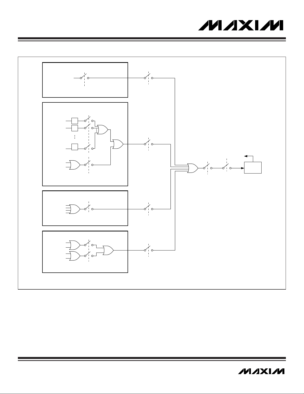
MAXQ7665/MAXQ7666 User’s Guide
1-25 __________________________________________________________________________________________________________
Figure 1-13. MAXQ7665/MAXQ7666 Interrupt Source Hierarchy Example
SYSTEM MODULES
WDIF
(WATCHDOG)
EWDI
(LOCAL ENABLE)
MODULE 0
IE0
ƒ
IE1
IE7
ƒ
ƒ
EX0-EX7
RI
TI
ESI
(LOCAL ENABLES)
IMS
(SYSTEM ENABLE)
IM0
(MODULE 0 ENABLE)
IGE
(GLOBAL ENABLE)
INS
(INTERRUPT IN SERVICE)
INTERRUPT
VECTOR
MODULE 1
SPIC
ROVR
WCOL
MODF
T2CL
TF2CL
TCC2
TF2
NOTE: ONLY A FEW OF THE MANY POSSIBLE MAXQ PERIPHERAL MODULES ARE SHOWN IN THIS INTERRUPT
HIERARCHY FIGURE.
ESPII
(LOCAL ENABLE)
MODULE 2
ET2L, ET2
(LOCAL ENABLES)
IM1
(MODULE 1 ENABLE)
IM2
(MODULE 2 ENABLE)
Page 28

1.2.4.4 Interrupt Prioritization by Software
All interrupt sources of the MAXQ7665/MAXQ7666 microcontrollers naturally have the same priority. However, when CPU operation vectors to the programmed Interrupt Vector address, the order in which potential interrupt sources are interrogated is left entirely up to the
user, as this often depends upon the system design and application requirements. The Interrupt Mask system register provides the ability to knowingly block interrupts from modules considered to be of lesser priority and manually re-enable the interrupt servicing by the
CPU (by setting INS = 0). Using this procedure, a given interrupt service routine can continue executing, only to be interrupted by higher priority interrupts. An example demonstrating this software prioritization is provided in
Section 1.3.8: Handling Interrupts
.
1.2.4.5 Interrupt Exception Window
An interrupt exception window is a noninterruptable execution cycle. During this cycle, the interrupt handler does not respond to any interrupt requests. All interrupts that would normally be serviced during an interrupt exception window are delayed until the next execution cycle.
Interrupt exception windows are used when two or more instructions must be executed consecutively without any delays in between.
Currently, there is a single condition in the MAXQ7665/MAXQ7666 microcontrollers that causes an interrupt exception window: activation of the prefix (PFX) register.
When the prefix register is activated by writing a value to it, it retains that value only for the next clock cycle. For the prefix value to be
used properly by the next instruction, the instruction that sets the prefix value and the instruction that uses it must always be executed back to back. Therefore, writing to the PFX register causes an interrupt exception window on the next cycle. If an interrupt occurs
during an interrupt exception window, an additional latency of one cycle in the interrupt handling will be caused as the interrupt will
not be serviced until the next cycle.
1.2.4.6 MAXQ7665/MAXQ7666 Interrupt Sources
Table 1-6 lists all possible interrupt sources for the MAXQ7665/MAXQ7666, along with their corresponding module interrupt enable bits,
local interrupt enable bits, and interrupt flags.
• Each module interrupt enable bit, when cleared to 0, will block interrupts originating in that module from being acknowledged.
When the module interrupt enable bit is set to 1, interrupts from that module are acknowledged (unless the interrupts have been
disabled globally).
• Each local interrupt enable bit, when cleared to 0, will disable the corresponding interrupt. When the local interrupt enable bit
is set to 1, the interrupt will be triggered whenever the interrupt flag is set to 1 (either by software or hardware).
• All interrupt flag bits cause the corresponding interrupt to trigger when the bit is set to 1. These bits are typically set by hardware and must be cleared by software (generally in the interrupt handler routine).
Note that for an interrupt to fire, the following five conditions must exist:
1) Interrupts must be enabled globally by setting IGE (IC.0) to 1.
2) The module interrupt enable bit for that interrupt source’s module must be set to 1.
3) The local interrupt enable bit for that specific interrupt source must be set to 1.
4) The interrupt flag for that interrupt source must be set to 1. Typically, this is done by hardware when the condition that requires
interrupt service occurs.
5) The Interrupt In Service (INS) bit must be cleared to 0. This bit is set automatically upon vectoring to the interrupt handler
address and cleared automatically upon exit (RETI/POPI), so the only reason to clear this bit manually (inside the interrupt handler routine) is allow nested interrupt handling.
MAXQ7665/MAXQ7666 User’s Guide
__________________________________________________________________________________________________________ 1-26
Page 29

MAXQ7665/MAXQ7666 User’s Guide
1-27 __________________________________________________________________________________________________________
Table 1-6. MAXQ7665/MAXQ7666 Interrupt Sources and Control Bits
INTERRUPT MODULE ENABLE BIT LOCAL ENABLE BIT INTERRUPT FLAG
Watchdog Interrupt IMS (IMR.7) EWDI (WDCN.6) WDIF (WDCN.3)
External Interrupt 0 IM0 (IMR.0) EX0 (EIE0.0) IE0 (EIF0.0)
External Interrupt 1 IM0 (IMR.0) EX1 (EIE0.1) IE1 (EIF0.1)
External Interrupt 2 IM0 (IMR.0) EX2 (EIE0.2) IE2 (EIF0.2)
External Interrupt 3 IM0 (IMR.0) EX3 (EIE0.3) IE3 (EIF0.3)
External Interrupt 4 IM0 (IMR.0) EX4 (EIE0.4) IE4 (EIF0.4)
External Interrupt 5 IM0 (IMR.0) EX5 (EIE0.5) IE5 (EIF0.5)
External Interrupt 6 IM0 (IMR.0) EX6 (EIE0.6) IE6 (EIF0.6)
External Interrupt 7 IM0 (IMR.0) EX7 (EIE0.7) IE7 (EIF0.7)
Serial Port Receive IM0 (IMR.0) ESI (SMD0.2) RI (SCON0.0)
Serial Port Transmit IM0 (IMR.0) ESI (SMD0.2) TI (SCON0.1)
SPI Mode Fault IM1 (IMR.1) ESPII (SPICF.7) MODF (SPICN.3)
SPI Write Collision IM1 (IMR.1) ESPII (SPICF.7) WCOL (SPICN.4)
SPI Receive Overrun IM1 (IMR.1) ESPII (SPICF.7) ROVR (SPICN.5)
SPI Transfer Complete IM1 (IMR.1) ESPII (SPICF.7) SPIC (SPICN.6)
Timer 0—Low Compare IM2 (I MR.2) ET2L (T2C NB0.7) T2CL (T2CNB0.0)
Timer 0—Low Overflow IM2 (IMR.2) ET2L (T2CNB0.7) TF2L (T2CN B0.2)
Timer 0—Capture/Compare IM2 (IMR.2) ET2 (T2CNA0.7) TCC2 (T2CNB0.1)
Timer 0—Overflow IM2 (IMR.2) ET2 (T2CNA0.7) TF2 (T2CNB0.3)
Timer 1—Low Compare IM2 (I MR.2) ET2L (T2C NB1.7) T2CL (T2CNB1.0)
Timer 1—Low Overflow IM2 (IMR.2) ET2L (T2CNB1.7) TF2L (T2CN B1.2)
Timer 1—Capture/Compare IM2 (IMR.2) ET2 (T2CNA1.7) TCC2 (T2CNB1.1)
Timer 1—Overflow IM2 (IMR.2) ET2 (T2CNA1.7) TF2 (T2CNB1.3)
Timer 2—Low Compare IM3 (I MR.3) ET2L (T2C NB2.7) T2CL (T2CNB2.0)
Timer 2—Low Overflow IM3 (IMR.3) ET2L (T2CNB2.7) TF2L (T2CN B2.2)
Timer 2—Capture/Compare IM3 (IMR.3) ET2 (T2CNA2.7) TCC2 (T2CNB2.1)
Timer 2—Overflow IM3 (IMR.3) ET2 (T2CNA2.7) TF2 (T2CNB2.3)
CAN 0 Message Center 1 Receive IM4 (IMR.4) ERI ( C0M1C.5) IN TRQ ( C0M1C.4)
CAN 0 Message Center 1 Transmit IM4 (IMR.4) ETI (C0M1C.6) INTRQ (C0M1C.4)
CAN 0 Message Center 2 Receive IM4 (IMR.4) ERI ( C0M2C.5) IN TRQ ( C0M2C.4)
CAN 0 Message Center 2 Transmit IM4 (IMR.4) ETI (C0M2C.6) INTRQ (C0M2C.4)
Page 30

MAXQ7665/MAXQ7666 User’s Guide
__________________________________________________________________________________________________________ 1-28
Table 1-6. MAXQ7665/MAXQ7666 Interrupt Sources and Control Bits (continued)
INTERRUPT MODULE ENABLE BIT LOCAL ENABLE BIT INTERRUPT FLAG
CAN 0 Message Center 3 Receive IM4 (IMR.4) ERI ( C0M3C.5) IN TRQ ( C0M3C.4)
CAN 0 Message Center 3 Transmit IM4 (IMR.4) ETI (C0M3C.6) INTRQ (C0M3C.4)
CAN 0 Message Center 4 Receive IM4 (IMR.4) ERI ( C0M4C.5) IN TRQ ( C0M4C.4)
CAN 0 Message Center 4 Transmit IM4 (IMR.4) ETI (C0M4C.6) INTRQ (C0M4C.4)
CAN 0 Message Center 5 Receive IM4 (IMR.4) ERI ( C0M5C.5) IN TRQ ( C0M5C.4)
CAN 0 Message Center 5 Transmit IM4 (IMR.4) ETI (C0M5C.6) INTRQ (C0M5C.4)
CAN 0 Message Center 6 Receive IM4 (IMR.4) ERI ( C0M6C.5) IN TRQ ( C0M6C.4)
CAN 0 Message Center 6 Transmit IM4 (IMR.4) ETI (C0M6C.6) INTRQ (C0M6C.4)
CAN 0 Message Center 7 Receive IM4 (IMR.4) ERI ( C0M7C.5) IN TRQ ( C0M7C.4)
CAN 0 Message Center 7 Transmit IM4 (IMR.4) ETI (C0M7C.6) INTRQ (C0M7C.4)
CAN 0 Message Center 8 Receive IM4 (IMR.4) ERI ( C0M8C.5) IN TRQ ( C0M8C.4)
CAN 0 Message Center 8 Transmit IM4 (IMR.4) ETI (C0M8C.6) INTRQ (C0M8C.4)
CAN 0 Message Center 9 Receive IM4 (IMR.4) ERI ( C0M9C.5) IN TRQ ( C0M9C.4)
CAN 0 Message Center 9 Transmit IM4 (IMR.4) ETI (C0M9C.6) INTRQ (C0M9C.4)
CAN 0 Message Center 10 Receive IM4 (IMR.4) ERI (C0M10C.5) INTRQ (C0M10C.4)
CAN 0 Message Center 10 Transmit IM4 (I MR.4) ETI (C0M10C.6) INTRQ (C0M10C.4)
CAN 0 Message Center 11 Receive IM4 (IMR.4) ERI (C0M11C.5) INTRQ (C0M11C.4)
CAN 0 Message Center 11 Transmit IM4 (I MR.4) ETI (C0M11C.6) INTRQ (C0M11C.4)
CAN 0 Message Center 12 Receive IM4 (IMR.4) ERI (C0M12C.5) INTRQ (C0M12C.4)
CAN 0 Message Center 12 Transmit IM4 (I MR.4) ETI (C0M12C.6) INTRQ (C0M12C.4)
CAN 0 Message Center 13 Receive IM4 (IMR.4) ERI (C0M13C.5) INTRQ (C0M13C.4)
CAN 0 Message Center 13 Transmit IM4 (I MR.4) ETI (C0M13C.6) INTRQ (C0M13C.4)
CAN 0 Message Center 14 Receive IM4 (IMR.4) ERI (C0M14C.5) INTRQ (C0M14C.4)
CAN 0 Message Center 14 Transmit IM4 (I MR.4) ETI (C0M14C.6) INTRQ (C0M14C.4)
CAN 0 Message Center 15 Receive IM4 (IMR.4) ERI (C0M15C.5) INTRQ (C0M15C.4)
CAN 0 Message Center 15 Transmit IM4 (I MR.4) ETI (C0M15C.6) INTRQ (C0M15C.4)
CAN 0 Bus Off Status IM4 (IMR.4) ERIE(C0C.7), C0IE (COR.0) BSS (C0S.7)
CAN 0 Er ror Count > 96/128 Status IM4 (IMR.4) ERIE( C0C.7), C0IE ( COR.0) EC 96/128 (C 0S.6)
CAN 0 Wake-Up Status IM4 (IMR.4) STIE(C0C.6), C0IE (COR.0) WKS (C0S.5)
CAN 0 Receive Status IM4 (IMR.4) STIE(C0C.6), C0IE (COR.0) RXS (C0S.4)
CAN 0 Transmit Status IM4 (IMR.4) STIE(C0C.6), C0IE (COR.0) TXS (C0S.3)
CAN 0 Bus Error Status IM4 (IMR.4) STIE(C0C.6), C0IE (COR.0) ER2:ER0 (C0S.2:C0S.0)
CAN 0 Bus Activity Status IM4 (IMR.4) C0BIE (COR.1) CAN0BA (COR.7)
ADC Data Ready IM5 (IMR.5) ADCIE (AIE.1) ADCRY (ASR.1)
ADC Overrun IM5 (IMR.5) AORIE (AIE.2) ADCOV (ASR.2)
Page 31

1.3 Programming
The following section provides a programming overview of the MAXQ7665/MAXQ7666. For full details on the instruction set, as well as
System Register and Peripheral Register detailed bit descriptions, see the appropriate sections in this user’s guide.
1.3.1 Addressing Modes
The instruction set for the MAXQ7665/MAXQ7666 provides three different addressing modes: direct, indirect, and immediate.
The direct addressing mode can be used to specify either source or destination registers, such as:
move A[0], A[1] ; copy accumulator 1 to accumulator 0
push A[0] ; push accumulator 0 on the stack
add A[1] ; add accumulator 1 to the active accumulator
Direct addressing is also used to specify addressable bits within registers.
move C, Acc.0 ; copy bit zero of the active accumulator
; to the carry flag
move PO0.3, #1 ; set bit three of port 0 Output register
Indirect addressing, in which a register contains a source or destination address, is used only in a few cases.
move @DP[0], A[0] ; copy accumulator 0 to the data memory
; location pointed to by data pointer 0
move A[0], @SP-- ; where @SP-- is used to pop the data pointed to
; by the stack pointer register
Immediate addressing is used to provide values to be directly loaded into registers or used as operands.
move A[0], #10h ; set accumulator 1 to 10h/16d
1.3.2 Prefixing Operations
All instructions on the MAXQ7665/MAXQ7666 are 16 bits long and execute in a single cycle. However, some operations require more
data than can be specified in a single cycle or require that high-order register-index bits be set to achieve the desired transfer. In these
cases, the prefix register module PFX is loaded with temporary data and/or required register index bits to be used by the following
instruction. The PFX module only holds loaded data for a single cycle before it clears to zero.
Instruction prefixing is required for the following operations, which effectively makes them two-cycle operations.
• When providing a 16-bit immediate value for an operation (e.g., loading a 16-bit register, ALU operation, supplying an absolute
program branch destination), the PFX module must be loaded in the previous cycle with the high byte of the 16-bit immediate
value unless that high byte is zero. One exception to this rule is when supplying an absolute branch destination to 00xxh. In
this case, PFX still must be written with 00h. Otherwise, the branch instruction would be considered a relative one instead of
the desired absolute branch.
• When selecting registers with indexes greater than 07h within a module as destinations for a transfer or registers with indexes
greater than 0Fh within a module as sources, the PFX[n] register must be loaded in the previous cycle. This can be combined
with the previous item.
MAXQ7665/MAXQ7666 User’s Guide
1-29 __________________________________________________________________________________________________________
Table 1-6. MAXQ7665/MAXQ7666 Interrupt Sources and Control Bits (continued)
INTERRUPT MODULE ENABLE BIT LOCAL ENABLE BIT INTERRUPT FLAG
Digital Brownout IM5 (IMR.5) DVBIE (AIE.4) DVBI (ASR.4)
I/O Voltage Brownout IM5 ( IMR.5) VIOBIE (AIE.5) VIOBI (ASR.5)
Hi gh-Frequency Oscillator Failu re IM5 (IMR.5) HFFIE (AIE.6) H FFINT (ASR.6)
Page 32

Generally, prefixing operations can be inserted automatically by the assembler as needed, so that (for example)
move DP[0], #1234h
actually assembles as
move PFX[0], #12h
move DP[0], #34h
However, the operation
move DP[0], #0055h
does not require a prefixing operation even though the register DP[0] is 16-bit. This is because the prefix value defaults to zero, so the line
move PFX[0], #00h
is not required.
1.3.3 Reading and Writing Registers
All functions in the MAXQ7665/MAXQ7666 are accessed through registers, either directly or indirectly. This section discusses loading
registers with immediate values and transferring values between registers of the same size and different sizes.
1.3.3.1 Loading an 8-Bit Register with an Immediate Value
Any writeable 8-bit register with a subindex from 0h to 7h within its module can be loaded with an immediate value in a single cycle
using the MOVE instruction.
move AP, #05h ; load accumulator pointer register with 5 hex
Writeable 8-bit registers with subindexes 8h and higher can be loaded with an immediate value using MOVE as well, but an additional cycle is required to set the prefix value for the destination.
move WDCN, #33h ; assembles to: move PFX[2], #00h
; move (WDCN-80h), #33h
1.3.3.2 Loading a 16-Bit Register with a 16-Bit Immediate Value
Any writeable 16-bit register with a subindex from 0h to 07h can be loaded with an immediate value in a single cycle if the high byte
of that immediate value is zero.
move LC[0], #0010h ; prefix defaults to zero for high byte
If the high byte of that immediate value is not zero or if the 16-bit destination subindex is greater than 7h, an extra cycle is required to
load the prefix value for the high byte and/or the high-order register index bits.
; high byte <> #00h
move LC[0], #0110h ; assembles to: move PFX[0], #01h
; move LC[0], #10h
; destination sub-index > 7h
move A[8], #0034h ; assembles to: move PFX[2], #00h
; move (A[8]-80h), #34h
1.3.3.3 Moving Values Between Registers of the Same Size
Moving data between same-size registers can be done in a single-cycle MOVE if the destination register’s index is from 0h to 7h and
the source register index is between 0h and Fh.
move A[0], A[8] ; copy accumulator 8 to accumulator 0
move LC[0], LC[1] ; copy loop counter 1 to loop counter 0
If the destination register’s index is greater than 7h or if the source register index is greater than Fh, prefixing is required.
move A[15], A[0] ; assembles to: move PFX[2], #00h
; move (A[15]-80h), A[0]
1.3.3.4 Moving Values Between Registers of Different Sizes
Before covering some transfer scenarios that might arise, a special register must be introduced that will be used in many of these
cases. The 16-bit General Register (GR) is expressly provided for performing byte singulation of 16-bit words. The high and low bytes
of GR are individually accessible in the GRH and GRL registers respectively. A read-only GRS register makes a byte-swapped version
of GR accessible and the GRXL register provides a sign-extended version of GRL.
MAXQ7665/MAXQ7666 User’s Guide
__________________________________________________________________________________________________________ 1-30
Page 33

1.3.3.4.1 8-Bit Destination ← Low Byte (16-Bit Source)
The simplest transfer possibility would be loading an 8-bit register with the low byte of a 16-bit register. This transfer does not require
use of GR and requires a prefix only if the destination or source register are outside of the single cycle write or read regions, 0–7h and
0–Fh, respectively.
move OFFS, LC[0] ; copy the low byte of LC[0] to the OFFS register
move IMR, @DP[1] ; copy the low byte @DP[1] to the IMR register
move WDCN, LC[0] ; assembles to: move PFX[2], #00h
; move (WDCN-80h), LC[0]
1.3.3.4.2 8-Bit Destination ← High Byte (16-Bit Source)
If, however, we needed to load an 8-bit register with the high byte of a 16-bit source, it would be best to use the GR register. Transferring
the 16-bit source to the GR register adds a single cycle.
move GR, LC[0] ; move LC[0] to the GR register
move IC, GRH ; copy the high byte into the IC register
1.3.3.4.3 16-Bit Destination ← Concatenation (8-Bit Source, 8-Bit Source)
Two 8-bit source registers can be concatenated and stored into a 16-bit destination by using the prefix register to hold the high-order
byte for the concatenated transfer. An additional cycle may be required if either source byte register index is greater than 0Fh or the
16-bit destination is greater than 07h.
move PFX[0], IC ; load high order source byte IC into PFX
move @DP[0], AP ; store @DP[0] the concatenation of IC:AP
; 16-bit destination sub-index: dst=08h
; 8-bit source sub-indexes:
; high=10h, low=11h
move PFX[1], #00h ;
move PFX[3], high ; PFX=00:high
move dst, low ; dst=high:low
1.3.3.4.4 Low (16-Bit Destination) ← 8-Bit Source
To modify only the low byte of a given 16-bit destination, the 16-bit register should be moved into the GR register such that the high
byte can be singulated and the low byte written exclusively. An additional cycle is required if the destination index is greater than 0Fh.
move GR, DP[0] ; move DP[0] to the GR register
move PFX[0], GRH ; get the high byte of DP[0] via GRH
move DP[0], #20h ; store the new DP[0] value
; 16-bit destination sub-index: dst=10h
; 8-bit source sub-index: src=11h
move PFX[1], #00h ;
move GR, dst ; read dst word to the GR register
move PFX[5], GRH ; get the high byte of dst via GRH
move dst, src ; store the new dst value
1.3.3.4.5 High (16-Bit Destination) ← 8-Bit Source
To modify only the high byte of a given 16-bit destination, the 16-bit register should be moved into the GR register such that the low
byte can be singulated and the high byte can be written exclusively. Additional cycles are required if the destination index is greater
than 0Fh or if the source index is greater than 0Fh.
move GR, DP[0] ; move DP[0] to the GR register
move PFX[0], #20h ; get the high byte of DP[0] via GRH
move DP[0], GRL ; store the new DP[0] value
; 16-bit destination sub-index: dst=10h
; 8-bit source sub-index: src=11h
move PFX[1], #00h ;
move GR, dst ; read dst word to the GR register
move PFX[1], #00h
move PFX[4], src ; get the new src byte
move dst, GRL ; store the new dst value
MAXQ7665/MAXQ7666 User’s Guide
1-31 __________________________________________________________________________________________________________
Page 34

If the high byte needs to be cleared to 00h, the operation can be shortened by transferring only the GRL byte to the 16-bit destination
(example follows):
move GR, DP[0] ; move DP[0] to the GR register
move DP[0], GRL ; store the new DP[0] value, 00h used for high byte
1.3.4 Reading and Writing Register Bits
The MOVE instruction can also be used to directly set or clear any one of the lowest 8 bits of a peripheral register in module 0h-5h or
a system register in module 8h. The set or clear operation will not affect the upper byte of a 16-bit register that is the target of the set
or clear operation. If a set or clear instruction is used on a destination register that does not support this type of operation, the register high byte will be written with the prefix data and the low byte will be written with the bit mask (i.e. all 0’s with a single 1 for the set
bit operation or all ones with a single 0 for the clear bit operation).
Register bits can be set or cleared individually using the MOVE instruction as follows.
move IGE, #1 ; set IGE (Interrupt Global Enable) bit
move APC.6, #0 ; clear IDS bit (APC.6)
As with other instructions, prefixing is required to select destination registers beyond index 07h.
The MOVE instruction may also be used to transfer any one of the lowest 8 bits from a register source or any bit of the active accumulator (Acc) to the Carry flag. There is no restriction on the source register module for the ‘MOVE C, src.bit’ instruction.
move C, IIR.3 ; copy IIR.3 to Carry
move C, Acc.7 ; copy Acc.7 to Carry
Prefixing is required to select source registers beyond index 15h.
1.3.5 Using the Arithmetic and Logic Unit
The MAXQ7665/MAXQ7666 provide a 16-bit (MAXQ20) ALU, which allows operations to be performed between the active accumulator and any other register. The ALU configuration provides 16 accumulator registers that are also 16 bits (MAXQ20) wide, of which any
one may be selected as the active accumulator.
1.3.5.1 Selecting the Active Accumulator
Any of the 16 accumulator registers A[0] through A[15] may be selected as the active accumulator by setting the low four bits of the
Accumulator Pointer Register (AP) to the index of the accumulator register you want to select.
move AP, #01h ; select A[1] as the active accumulator
move AP, #0Fh ; select A[15] as the active accumulator
The current active accumulator can be accessed as the Acc register, which is also the register used as the implicit destination for all
arithmetic and logical operations.
move A[0], #55h ; set A[0] = 55 hex (MAXQ10)
; = 0055 hex (MAXQ20)
move AP, #00h ; select A[0] as active accumulator
move Acc, #55h ; set A[0] = 55 hex (MAXQ10)
; = 0055 hex (MAXQ20)
1.3.5.2 Enabling Auto-Increment and Auto-Decrement
The accumulator pointer AP can be set to automatically increment or decrement after each arithmetic or logical operation. This is useful for operations involving a number of accumulator registers, such as adding or subtracting two multibyte integers.
If auto-increment/decrement is enabled, the AP register increments or decrements after any of the following operations:
• ADD src (Add source to active accumulator)
• ADDC src (Add source to active accumulator with carry)
• SUB src (Subtract source from active accumulator)
• SUBB src (Subtract source from active accumulator with borrow)
• AND src (Logical AND active accumulator with source)
• OR src (Logical OR active accumulator with source)
MAXQ7665/MAXQ7666 User’s Guide
__________________________________________________________________________________________________________ 1-32
Page 35
• XOR src (Logical XOR active accumulator with source)
• CPL (Bit-wise complement active accumulator)
• NEG (Negate active accumulator)
• SLA (Arithmetic shift left on active accumulator)
• SLA2 (Arithmetic shift left active accumulator two bit positions)
• SLA4 (Arithmetic shift left active accumulator four bit positions)
• SRA (Arithmetic shift right on active accumulator)
• SRA2 (Arithmetic shift right active accumulator two bit positions)
• SRA4 (Arithmetic shift right active accumulator four bit positions)
• RL (Rotate active accumulator left)
• RLC (Rotate active accumulator left through Carry flag)
• RR (Rotate active accumulator right)
• RRC (Rotate active accumulator right through Carry flag)
• SR (Logical shift active accumulator right)
• MOVE Acc, src (Copy data from source to active accumulator)
• MOVE dst, Acc (Copy data from active accumulator to destination)
• MOVE Acc, Acc (Recirculation of active accumulator contents)
• XCHN (Exchange nibbles within each byte of active accumulator)
• XCH (Exchange active accumulator bytes)
The active accumulator may not be the source in any instruction where it is also the implicit destination.
There is an additional notation that can be used to refer to the active accumulator for the instruction "MOVE dst, Acc." If the instruction
is instead written as "MOVE dst, A[AP]," the source value is still the active accumulator, but no AP auto-increment or auto-decrement
function will take place, even if this function is enabled. Note that the active accumulator may not be the destination for the MOVE dst,
A[AP] instruction (i.e., MOVE Acc, A[AP] is prohibited).
So, the two instructions
move A[7], Acc
move A[7], A[AP]
are equivalent, except that the first instruction triggers auto-increment/decrement (if it is enabled), while the second one will never do so.
The Accumulator Pointer Control Register (APC) controls the auto-increment/decrement mode as well as selects the range of bits (modulo) in the AP register that will be incremented or decremented. There are nine different unique settings for the APC register, as listed
in Table 1-7.
Table 1-7. Accumulator Pointer Control Register Settings
MAXQ7665/MAXQ7666 User’s Guide
1-33 __________________________________________________________________________________________________________
APC.2
(MOD2)
0 0 0 X 00h No auto-increment/decrement (default mode)
0 0 1 0 01h Increment bit 0 of AP (modulo 2)
0 0 1 1 41h Decrement bit 0 of AP (modulo 2)
0 1 0 0 02h Increment bits [1:0] of AP (modulo 4)
0 1 0 1 42h Decrement bits [1:0] of AP (modulo 4)
0 1 1 0 03h Increment bits [2:0] of AP (modulo 8)
0 1 1 1 43h Decrement bits [2:0] of AP (modulo 8)
1 0 0 0 04h Increment all 4 bits of AP (modulo 16)
1 0 0 1 44h Decrement all 4 bits of AP (modulo 16)
APC.1
(MOD1)
APC.0
(MOD0)
APC.6
(IDS)
APC AUTO-INCREMENT/DECREMENT SETTING
Page 36

For the modulo increment or decrement operation, the selected range of bits in AP are incremented or decremented. However, if these
bits roll over or under, they simply wrap around without affecting the remaining bits in the accumulator pointer. So, the operations can
be defined as follows:
• Increment modulo 2: AP = AP[3:1] + ((AP[0] + 1) mod 2)
• Decrement modulo 2: AP = AP[3:1] + ((AP[0] - 1) mod 2)
• Increment modulo 4: AP = AP[3:2] + ((AP[1:0] + 1) mod 4)
• Decrement modulo 4: AP = AP[3:2] + ((AP[1:0] - 1) mod 4)
• Increment modulo 8: AP = AP[3] + ((AP[2:0] + 1) mod 8)
• Decrement modulo 8: AP = AP[3] + ((AP[2:0] - 1) mod 8)
• Increment modulo 16: AP = (AP + 1) mod 16
• Decrement modulo 16: AP = (AP - 1) mod 16
For this example, assume that all 16 accumulator registers are initially set to zero.
move AP, #02h ; select A[2] as active accumulator
move APC, #02h ; auto-increment AP[1:0] modulo 4
; AP A[0] A[1] A[2] A[3]
; 02 0000 0000 0000 0000
add #01h ; 03 0000 0000 0001 0000
add #02h ; 00 0000 0000 0001 0002
add #03h ; 01 0003 0000 0001 0002
add #04h ; 02 0003 0004 0001 0002
add #05h ; 03 0003 0004 0006 0002
1.3.5.3 ALU Operations Using the Active Accumulator and a Source
The following arithmetic and logical operations can use any register or immediate value as a source. The active accumulator Acc is
always used as the second operand and the implicit destination. Also, Acc may not be used as the source for any of these operations.
add A[4] ; Acc = Acc + A[4]
addc #32h ; Acc = Acc + 0032h + Carry
sub A[15] ; Acc = Acc – A[15]
subb A[1] ; Acc = Acc – A[1] - Carry
cmp #00h ; If (Acc == 0000h), set Equals flag
and A[0] ; Acc = Acc AND A[0]
or #55h ; Acc = Acc OR #0055h
xor A[1] ; Acc = Acc XOR A[1]
MAXQ7665/MAXQ7666 User’s Guide
__________________________________________________________________________________________________________ 1-34
Page 37

1.3.5.4 ALU Operations Using Only the Active Accumulator
The following arithmetic and logical operations operate only on the active accumulator.
cpl ; Acc = NOT Acc
neg ; Acc = (NOT Acc) + 1
rl ; Rotate accumulator left (not using Carry)
rlc ; Rotate accumulator left through Carry
rr ; Rotate accumulator right (not using Carry)
rrc ; Rotate accumulator right through Carry
sla ; Shift accumulator left arithmetically once
sla2 ; Shift accumulator left arithmetically twice
sla4 ; Shift accumulator left arithmetically four times
sr ; Shift accumulator right, set Carry to Acc.0,
; set Acc.15 to zero (MAXQ20)
sra ; Shift accumulator right arithmetically once
sra2 ; Shift accumulator right arithmetically twice
sra4 ; Shift accumulator right arithmetically four times
xchn ; Swap low and high nibbles of each Acc byte
xch (MAXQ20 only) ; Swap low byte and high byte of Acc
1.3.5.5 ALU Bit Operations Using Only the Active Accumulator
The following operations operate on single bits of the current active accumulator in conjunction with the Carry flag. Any of these operations may use an Acc bit from 0 to 15.
move C, Acc.0 ; copy bit 0 of accumulator to Carry
move Acc.5, C ; copy Carry to bit 5 of accumulator
and Acc.3 ; Acc.3 = Acc.3 AND Carry
or Acc.0 ; Acc.0 = Acc.0 OR Carry
xor Acc.1 ; Acc.1 = Acc.1 OR Carry
None of the above bit operations cause the auto-increment, auto-decrement, or modulo operations defined by the accumulator pointer control (APC) register.
1.3.5.6 Example: Adding Two 4-Byte Numbers Using Auto-Increment
move A[0], #5678h ; First number – 12345678h
move A[1], #1234h
move A[2], #0AAAAh ; Second number – 0AAAAAAAh
move A[3], #0AAAh
move APC, #81h ; Active Acc = A[0], increment low bit = mod 2
add A[2] ; A[0] = 5678h + AAAAh = 0122h + Carry
addc A[3] ; A[1] = 1234h + AAAh + 1 = 1CDFh
; 12345678h + 0AAAAAAAh = 1CDF0122h
1.3.6 Processor Status Flag Operations
The Processor Status Flag (PSF) register contains five flags that are used to indicate and store the results of arithmetic and logical operations, four of which can also be used for conditional program branching.
1.3.6.1 Sign Flag
The Sign flag (PSF.6) reflects the current state of the high bit of the active accumulator (Acc.15 for the MAXQ20). If signed arithmetic
is being used, this flag indicates whether the value in the accumulator is positive or negative.
Since the Sign flag is a dynamic reflection of the high bit of the active accumulator, any instruction that changes the value in the active
accumulator can potentially change the value of the Sign flag. Also, any instruction that changes which accumulator is the active one
(including AP auto-increment/decrement) can also change the Sign flag.
The following operation uses the Sign flag:
• JUMP S, src (Jump if Sign flag is set)
MAXQ7665/MAXQ7666 User’s Guide
1-35 __________________________________________________________________________________________________________
Page 38

1.3.6.2 Zero Flag
The Zero flag (PSF.7) is a dynamic flag that reflects the current state of the active accumulator Acc. If all bits in the active accumulator are zero, the Zero flag equals 1. Otherwise, it equals 0.
Since the Zero flag is a dynamic reflection of (Acc = 0), any instruction that changes the value in the active accumulator can potentially change the value of the Zero flag. Also, any instruction that changes which accumulator is the active one (including AP auto-increment/decrement) can also change the Zero flag.
The following operations use the Zero flag:
• JUMP Z, src (Jump if Zero flag is set)
• JUMP NZ, src (Jump if Zero flag is cleared)
1.3.6.3 Equals Flag
The Equals flag (PSF.0) is a static flag set by the CMP instruction. When the source given to the CMP instruction is equal to the active
accumulator, the Equals flag is set to 1. When the source is different from the active accumulator, the Equals flag is cleared to 0.
The following instructions use the value of the Equals flag. Please note that the ‘src’ for the JUMP E/NE instructions must be immediate.
• JUMP E, src (Jump if Equals flag is set)
• JUMP NE, src (Jump if Equals flag is cleared)
In addition to the CMP instruction, any instruction using PSF as the destination can alter the Equals flag.
1.3.6.4 Carry Flag
The Carry flag (PSF.1) is a static flag indicating that a carry or borrow bit resulted from the last ADD/ADDC or SUB/SUBB operation.
Unlike the other status flags, it can be set or cleared explicitly and is also used as a generic bit operand by many other instructions.
The following instructions can alter the Carry flag:
• ADD src (Add source to active accumulator)
• ADDC src (Add source and Carry to active accumulator)
• SUB src (Subtract source from active accumulator)
• SUBB src (Subtract source and Carry from active accumulator)
• SLA, SLA2, SLA4 (Arithmetic shift left active accumulator)
• SRA, SRA2, SRA4 (Arithmetic shift right active accumulator)
• SR (Shift active accumulator right)
• RLC/RRC (Rotate active accumulator left / right through Carry)
• MOVE C, Acc.<b> (Set Carry to selected active accumulator bit)
• MOVE C, #i (Explicitly set, i = 1, or clear, i = 0, the Carry flag)
• CPL C (Complement Carry)
• AND Acc.<b>
• OR Acc.<b>
• XOR Acc.<b>
• MOVE C, src.<b> (Copy bit addressable register bit to Carry)
• any instruction using PSF as the destination
The following instructions use the value of the Carry flag:
• ADDC src (Add source and Carry to active accumulator)
• SUBB src (Subtract source and Carry from active accumulator)
• RLC/RRC (Rotate active accumulator left/right through Carry)
• CPL C (Complement Carry)
MAXQ7665/MAXQ7666 User’s Guide
__________________________________________________________________________________________________________ 1-36
Page 39

• MOVE Acc.<b>, C (Set selected active accumulator bit to Carry)
• AND Acc.<b> (Carry = Carry AND selected active accumulator bit)
• OR Acc.<b> (Carry = Carry OR selected active accumulator bit)
• XOR Acc.<b> (Carry = Carry XOR selected active accumulator bit)
• JUMP C, src (Jump if Carry flag is set)
• JUMP NC, src (Jump if Carry flag is cleared)
1.3.6.5 Overflow Flag
The Overflow flag (PSF.2) is a static flag indicating that the carry or borrow bit (Carry status Flag) resulting from the last ADD/ADDC or
SUB/SUBB operation did not match the carry or borrow of the high order bit of the active accumulator. The overflow flag is useful when
performing signed arithmetic operations.
The following instructions can alter the Overflow flag:
• ADD src (Add source to active accumulator)
• ADDC src (Add source and Carry to active accumulator)
• SUB src (Subtract source from active accumulator)
• SUBB src (Subtract source and Carry from active accumulator)
1.3.7 Controlling Program Flow
The MAXQ7665/MAXQ7666 provide several options to control program flow and branching. Jumps may be unconditional, conditional, relative, or absolute. Subroutine calls store the return address on the hardware stack for later return. Built-in counters and address
registers are provided to control looping operations.
1.3.7.1 Obtaining the Next Execution Address
The address of the next instruction to be executed can be read at any time by reading the Instruction Pointer (IP) register. This can be
particularly useful for initializing loops. Note that the value returned is actually the address of the current instruction plus 1, so this will
be the address of the next instruction executed as long as the current instruction does not cause a jump.
1.3.7.2 Unconditional Jumps
An unconditional jump can be relative (IP +127/-128 words) or absolute (to anywhere in program space). Relative jumps must use an
8-bit immediate operand, such as
Label1: ; must be within +127/-128 words of the JUMP
...
jump Label1
Absolute jumps can use a 16-bit immediate operand, a 16-bit register, or an 8-bit register.
jump LongJump ; assembles to: move PFX[0], #high(LongJump)
; jump #low(LongJump)
jump DP[0] ; absolute jump to the address in DP[0]
If an 8-bit register is used as the jump destination, the prefix value is used as the high byte of the address and the register is used as
the low byte.
MAXQ7665/MAXQ7666 User’s Guide
1-37 __________________________________________________________________________________________________________
Page 40

1.3.7.3 Conditional Jumps
Conditional jumps transfer program execution based on the value of one of the status flags (C, E, Z, S). Except where noted for JUMP
E and JUMP NE, the absolute and relative operands allowed are the same as for the unconditional JUMP command.
jump c, Label1 ; jump to Label1 if Carry is set
jump nc, LongJump ; jump to LongJump if Carry is not set
jump z, LC[0] ; jump to 16-bit register destination if
; Zero is set
jump nz, Label1 ; jump to Label1 if Zero is not set (Acc<>0)
jump s, A[2] ; jump to A[2] if Sign flag is set
jump e, Label1 ; jump to Label1 if Equal is set
jump ne, Label1 ; jump to Label1 if Equal is cleared
JUMP E and JUMP NE may only use immediate destinations.
1.3.7.4 Calling Subroutines
The CALL instruction works the same as the unconditional JUMP, except that the next execution address is pushed on the stack before
transferring program execution to the branch address. The RET instruction is used to return from a normal call, and RETI is used to
return from an interrupt handler routine.
call Label1 ; if Label1 is relative,
; assembles to : call #immediate
call LongCall ; assembles to: move PFX[0], #high(LongCall)
; call #low(LongCall)
call LC[0] ; call to address in LC[0]
LongCall:
ret ; return from subroutine
1.3.7.5 Looping Operations
Looping over a section of code can be performed by using the conditional jump instructions. However, there is built-in functionality, in
the form of the ‘DJNZ LC[n], src’ instruction, to support faster, more compact looping code with separate loop counters. The 16-bit registers LC[0], and LC[1] are used to store these loop counts. The ‘DJNZ LC[n], src’ instruction automatically decrements the associated loop counter register and jumps to the loop address specified by src if the loop counter has not reached 0.
To initialize a loop, set the LC[n] register to the count you wish to use before entering the loop’s main body.
The desired loop address should be supplied in the src operand of the ‘DJNZ LC[n], src’ instruction. When the supplied loop address
is relative (+127/-128 words) to the DJNZ LC[n] instruction, as is typically the case, the assembler automatically calculates the relative
offset and inserts this immediate value in the object code.
move LC[1], #10h ; loop 16 times
LoopTop: ; loop addr relative to djnz LC[n],src instruction
call LoopSub
djnz LC[1], LoopTop ; decrement LC[1] and jump if nonzero
When the supplied loop address is outside the relative jump range, the prefix register (PFX[0]) is used to supply the high byte of the
loop address as required.
move LC[1], #10h ; loop 16 times
LoopTop: ; loop addr not relative to djnz LC[n],src
call LoopSub
...
djnz LC[1], LoopTop ; decrement LC[1] and jump if nonzero
; assembles to: move PFX[0], #high(LoopTop)
; djnz LC[1], #low(LoopTop)
MAXQ7665/MAXQ7666 User’s Guide
__________________________________________________________________________________________________________ 1-38
Page 41

If loop execution speed is critical and a relative jump cannot be used, one might consider preloading an internal 16-bit register with
the src loop address for the ‘DJNZ LC[n], src’ loop. This ensures that the prefix register will not be needed to supply the loop address
and always yields the fastest execution of the DJNZ instruction.
move LC[0], #LoopTop ; using LC[0] as address holding register
; assembles to: move PFX[0], #high(LoopTop)
; move LC[0], #low(LoopTop)
move LC[1], #10h ; loop 16 times
...
LoopTop: ; loop address not relative to djnz LC[n],src
call LoopSub
...
djnz LC[1], LC[0] ; decrement LC[1] and jump if nonzero
If opting to preload the loop address to an internal 16-bit register, the most time and code efficient means is by performing the load in
the instruction just prior to the top of the loop:
move LC[1], #10h ; Set loop counter to 16
move LC[0], IP ; Set loop address to the next address
LoopTop: ; loop addr not relative to djnz LC[n],src
...
1.3.7.6 Conditional Returns
Similar to the conditional jumps, the MAXQ7665/MAXQ7666 microcontrollers also support a set of conditional return operations. Based
upon the value of one of the status flags, the CPU can conditionally pop the stack and begin execution at the address popped from
the stack. If the condition is not true, the conditional return instruction does not pop the stack and does not change the instruction pointer. The following conditional return operations are supported:
RET C ; if C=1, a RET is executed
RET NC ; if C=0, a RET is executed
RET Z ; if Z=1 (Acc=00h), a RET is executed
RET NZ ; if Z=0 (Acc<>00h), a RET is executed
RET S ; if S=1, a RET is executed
1.3.8 Handling Interrupts
Handling interrupts in the MAXQ7665/MAXQ7666 is a three-part process. First, the location of the interrupt handling routine must be
set by writing the address to the 16-bit Interrupt Vector (IV) register. This register defaults to 0000h on reset, but this will usually not be
the desired location since this will often be the location of reset/power-up code.
move IV, IntHandler ; move PFX[0], #high(IntHandler)
; move IV, #low(IntHandler)
; PFX[0] write not needed if IntHandler addr=00xxh
Next, the interrupt must be enabled. For any interrupts to be handled, the IGE bit in the Interrupt and Control register (IC) must first be
set to 1. Next, the interrupt itself must be enabled at the module level and locally within the module itself. The module interrupt enable
is located in the Interrupt Mask register, while the location of the local interrupt enable will vary depending on the module in which the
interrupt source is located.
Once the interrupt handler receives the interrupt, the Interrupt in Service (INS) bit will be set by hardware to block further interrupts,
and execution control is transferred to the interrupt service routine. Within the interrupt service routine, the source of the interrupt must
be determined. Since all interrupts go to the same interrupt service routine, the Interrupt Identification Register (IIR) must be examined
to determine which module initiated the interrupt. For example, the II0 (IIR.0) bit will be set if there is a pending interrupt from module
0. These bits cannot be cleared directly; instead, the appropriate bit flag in the module must be cleared once the interrupt is handled.
MAXQ7665/MAXQ7666 User’s Guide
1-39 __________________________________________________________________________________________________________
Page 42

INS is set automatically on entry to the interrupt handler and cleared automatically on exit (RETI).
IntHandler:
push PSF ; save C since used in identification process
move C, IIR.X ; check highest priority flag in IIR
jump C, ISR_X ; if IIR.X is set, interrupt from module X
move C, IIR.Y ; check next highest priority int source
jump C, ISR_Y ; if IIR.Y is set, interrupt from module Y
...
ISR_X:
...
reti
To support high priority interrupts while servicing another interrupt source, the IMR register may be used to create a user-defined prioritization. The IMR mask register should not be utilized when the highest priority interrupt is being serviced because the highest priority
interrupt should never be interrupted. This is default condition when a hardware branch is made the Interrupt Vector address (INS is set
to 1 by hardware and all other interrupt sources are blocked). The code below demonstrates how to use IMR to allow other interrupts.
ISR_Z:
pop PSF ; restore PSF
push IMR ; save current interrupt mask
move IMR, #int_mask ; new mask to allow only higher priority ints
move INS, #0 ; re-enable interrupts
...
(interrupt servicing code)
...
pop IMR ; restore previous interrupt mask
ret ; back to code or lower priority interrupt
Please note that configuring a given IMR register mask bit to 0 only prevents interrupt conditions from the corresponding module or system from generating an interrupt request. Configuring an IMR mask bit to 0 does not prevent the corresponding IIR system or module identification flag from being set. This means that when using the IMR mask register functionality to block interrupts, there may be cases when
both the mask (IMR.x) and identifier (IIR.x) bits should be considered when determining if the corresponding peripheral should be serviced.
1.3.8.1 Conditional Return from Interrupt
Similar to the conditional returns, the MAXQ7665/MAXQ7666 microcontrollers also support a set of conditional return from interrupt
operations. Based upon the value of one of the status flags, the CPU can conditionally pop the stack, clear the INS bit to 0, and begin
execution at the address popped from the stack. If the condition is not true, the conditional return from interrupt instruction leaves the
INS bit unchanged, does not pop the stack and does not change the instruction pointer. The following conditional return from interrupt
operations are supported:
RETI C ; if C=1, a RETI is executed
RETI NC ; if C=0, a RETI is executed
RETI Z ; if Z=1 (Acc=00h), a RETI is executed
RETI NZ ; if Z=0 (Acc<>00h), a RETI is executed
RETI S ; if S=1, a RETI is executed
1.3.9 Accessing the Stack
The hardware stack is used automatically by the CALL, RET and RETI instructions, but it can also be used explicitly to store and retrieve
data. All values stored on the stack are 16 bits wide.
The PUSH instruction increments the stack pointer SP and then stores a value on the stack. When pushing a 16-bit value onto the stack,
the entire value is stored. However, when pushing an 8-bit value onto the stack, the high byte stored on the stack comes from the prefix register. The @++SP stack access mnemonic is the associated destination specifier that generates this push behavior, thus the following two instruction sequences are equivalent:
move PFX[0], IC
push PSF ; stored on stack: IC:PSF
move PFX[0], IC
move @++SP, PSF ; stored on stack: IC:PSF
MAXQ7665/MAXQ7666 User’s Guide
__________________________________________________________________________________________________________ 1-40
Page 43

The POP instruction removes a value from the stack and then decrements the stack pointer. The @SP-- stack access mnemonic is the
associated source specifier that generates this behavior, thus the following two instructions are equivalent:
pop PSF
move PSF, @SP--
The POPI instruction is equivalent to the POP instruction but additionally clears the INS bit to 0. Thus, the following two instructions
would be equivalent:
popi IP
reti
The @SP-- mnemonic can be used by the MAXQ microcontroller so that stack values may be used directly by ALU operations (e.g.
ADD src, XOR src, etc.) without requiring that the value be first popped into an intermediate register or accumulator.
add @SP-- ; sum the last three words pushed onto the stack
add @SP-- ; with Acc, disregarding overflow
add @SP--
The stack pointer SP can be set explicitly, however only those least significant bits needed to represent the stack depth for the associated MAXQ device are used. For a MAXQ device that has a stack depth of 16 words, only the lowest four bits are used and setting
SP to 0Fh will return it to its reset state.
Since the stack is 16 bits wide, it is possible to store two 8-bit register values on it in a single location. This allows more efficient use
of the stack if it is being used to save and restore registers at the start and end of a subroutine.
SubOne:
move PFX[0], IC
push PSF ; store IC:PSF on the stack
...
pop GR ; 16-bit register
move IC, GRH ; IC was stored as high byte
move PSF, GRL ; PSF was stored as low byte
ret
1.3.10 Accessing Data Memory
Data memory is accessed through the data pointer registers DP[0] and DP[1] or the Frame Pointer BP[OFFS]. Once one of these registers is set to a location in data memory, that location can be read or written as follows, using the mnemonic @DP[0], @DP[1], or
@BP[OFFS] as a source or destination.
move DP[0], #0000h ; set pointer to location 0000h
move A[0], @DP[0] ; read from data memory
move @DP[0], #55h ; write to data memory
Either of the data pointers may be post-incremented or post-decremented following any read or may be pre-incremented or pre-decremented before any write access by using the following syntax.
move A[0], @DP[0]++ ; increment DP[0] after read
move @++DP[0], A[1] ; increment DP[0] before write
move A[5], @DP[1]-- ; decrement DP[1] after read
move @--DP[1], #00h ; decrement DP[1] before write
The Frame Pointer (BP[OFFS]) is actually composed of a base pointer (BP) and an offset from the base pointer (OFFS). For the frame
pointer, the offset register (OFFS) is the target of any increment or decrement operation. The base pointer (BP) is unaffected by increment and decrement operations on the Frame Pointer. Similar to DP[n], the OFFS register may be pre-incremented/decremented when
writing to data memory and may be post-incremented/decremented when reading from data memory.
move A[0], @BP[OFFS--] ; decrement OFFS after read
move @BP[++OFFS], A[1] ; increment OFFS before write
All three data pointers support both byte and word access to data memory. Each data pointer has its own word/byte select (WBSn)
special-function register bit to control the access mode associated with the data pointer. These three register bits (WBS2, which controls BP[OFFS] access; WBS1, which controls DP[1] access; and WBS0, which controls DP[0] access) reside in the Data Pointer
Control (DPC) register. When a given WBSn control bit is configured to 1, the associated pointer is operated in the word access mode.
When the WBSn bit is configured to 0, the pointer is operated in the byte access mode. Word access mode allows addressing of
64kWords of memory while byte access mode allows addressing of 64kBytes of memory.
MAXQ7665/MAXQ7666 User’s Guide
1-41 __________________________________________________________________________________________________________
Page 44

Each data pointer (DP[n]) and Frame Pointer base (BP) register is actually implemented internally as a 17-bit register (e.g., 16:0). The Frame
Pointer offset register (OFFS) is implemented internally as a 9-bit register (e.g., 8:0). The WBSn bit for the respective pointer controls whether
the highest 16 bits (16:1) of the pointer are in use, as is the case for word mode (WBSn = 1) or whether the lowest 16 bits (15:0) are in use,
as will be the case for byte mode (WBSn = 0). The WBS2 bit also controls whether the high 8 bits (8:1) of the offset register are in use
(WBS2 = 1) or the low 8 bits (7:0) are used (WBS2 = 0). All data pointer register reads, writes, auto-increment/decrement operations occur
with respect to the current WBSn selection. Data pointer increment and decrement operations only affect those bits specific to the current
word or byte addressing mode (e.g., incrementing a byte mode data pointer from FFFFh does not carry into the internal high order bit that
is utilized only for word mode data pointer access). Switching from byte to word access mode or vice versa does not alter the data pointer
contents. Therefore, it is important to maintain the consistency of data pointer address value within the given access mode.
move DPC, #0 ; DP[0] in byte mode
move DP[0], #2345h ; DP[0]=2345h (byte mode)
; internal bits 15:0 loaded
move DPC, #4 ; DP[0] in word mode
move DP[0], #2345h ; DP[0]=2345h (word mode)
; internal bits 16:1 loaded
move DPC, #0 ; DP[0] in byte mode
move GR, DP[0] ; GR = 468Bh (looking at bits 15:0)
The three pointers share a single read/write port on the data memory and thus, the user must knowingly activate a desired pointer
before using it for data memory read operations. This can be done explicitly using the data pointer select bits (SDPS1:0; DPC.1:0), or
implicitly by writing to the DP[n], BP, or OFFS registers as shown below. Any indirect memory write operation using a data pointer will
set the SDPS bits, thus activating the write pointer as the active source pointer.
move DPC, #2 ; (explicit) selection of FP as the pointer
move DP[1], DP[1] ; (implicit) selection of DP[1]; set SDPS1:0=01b
move OFFS, src ; (implicit) selection of FP; set SDPS1=1
move @DP[0], src ; (implicit) selection of DP[0]; set SDPS1:0=00b
Once the pointer selection has been made, it will remain in effect until:
• the source data pointer select bits are changed via the explicit or implicit methods described above (i.e., another data pointer
is selected for use)
• the memory to which the active source data pointer is addressing is enabled for code fetching using the Instruction Pointer, or
• a memory write operation is performed using a data pointer other than the current active source pointer.
move DP[1], DP[1] ; select DP[1] as the active pointer
move dst, @DP[1] ; read from pointer
move @DP[1], src ; write using a data pointer
; DP[0] is needed
move DP[0], DP[0] ; select DP[0] as the active pointer
To simplify data pointer increment/decrement operations without disturbing register data, a virtual NUL destination has been assigned
to system module 6, subindex 7 to serve as a bit bucket. Data pointer increment/decrement operations can be done as follows without altering the contents of any other register:
move NUL, @DP[0]++ ; increment DP[0]
move NUL, @DP[0]-- ; decrement DP[0]
The following data pointer related instructions are invalid:
move @++DP[0], @DP[0]++
move @++DP[1], @DP[1]++
move @BP[++Offs], @BP[Offs++]
move @--DP[0], @DP[0]-move @--DP[1], @DP[1]-move @BP[--Offs], @BP[Offs--]
move @++DP[0], @DP[0]-move @++DP[1], @DP[1]-move @BP[++Offs], @BP[Offs--]
move @--DP[0], @DP[0]++
move @--DP[1], @DP[1]++
MAXQ7665/MAXQ7666 User’s Guide
__________________________________________________________________________________________________________ 1-42
Page 45

move @BP[--Offs], @BP[Offs++]
move @DP[0], @DP[0]++
move @DP[1], @DP[1]++
move @BP[Offs], @BP[Offs++]
move @DP[0], @DP[0]-move @DP[1], @DP[1]-move @BP[Offs], @BP[Offs--]
move DP[0], @DP[0]++
move DP[0], @DP[0]-move DP[1], @DP[1]++
move DP[1], @DP[1]-move Offs, @BP[Offs--]
move Offs, @BP[Offs++]
1.4 System Register Descriptions
The MAXQ7665/MAXQ7666 system register map is shown in Table 1-8. The system register bit functions and reset value are shown in
Table 1-9. Those registers defined in the MAXQ7665/MAXQ7666 system register map are described in the following sections. The
address for each register are given in the format
module[index]
, where
module
is the module specifier from 8h to Fh and
index
is the
register subindex from 0h to Fh.
Table 1-8. MAXQ7665/MAXQ7666 System Register Map
MAXQ7665/MAXQ7666 User’s Guide
1-43 __________________________________________________________________________________________________________
Note: Names that appear in italics indicate that all bits of a register are read-only. Names that appear in bold indicate that a register is 16 bits wide.
CYCLES TO
READ
1 1 0h AP
1 1 1h APC
1 1 2h
1 1 3h
1 1 4h PSF
1 1 5h IC
1 1 6h IMR
1 1 7h
1 2 8h SC
1 2 9h
1 2 Ah
1 2 Bh IIR
1 2 Ch
1 2 Dh
1 2 Eh CKCN
1 2 Fh WDCN
CYCLES TO
WRITE
REGISTER
INDEX
AP (8h) A (9h) PFX (Bh) IP (Ch) SP (Dh) DPC (Eh) DP (Fh)
A[0] PFX[0] IP
A[1] PFX[1] SP
A[2] PFX[2] IV
A[3] PFX[3]
A[4] PFX[4] DPC
A[5] PFX[5] GR
A[6] PFX[6] LC0
A[7] PFX[7] LC1 BP DP1
A[8] GRS
A[9]
A[10]
A[11]
A[12]
A[13]
A[14]
A[15]
MODULE NAME (BASE SPECIFIER)
OFFS
GRL
GRH
GRXL
FP
DP0
Page 46

MAXQ7665/MAXQ7666 User’s Guide
__________________________________________________________________________________________________________ 1-44
Table 1-9. MAXQ7665/MAXQ7666 System Register Bit Functions and Reset Value
— — — — AP.3 AP.2 AP.1 AP.0
0 0 0 0 0 0 0 0
CLR IDS — — — MOD2 MOD1 MOD0
0 0 0 0 0 0 0 0
REGISTER BIT
1514131211109876543210
AP
REGISTER
08h[00h]
Z S — GPF1 GPF0 OV C E
PSF
APC
08h[01h]
1 0 0 0 0 0 0 0
— — CGDS — — — INS IGE
0 0 0 0 0 0 0 0
IMS — IM5 IM4 IM3 IM2 IM1 IM0
0 0 0 0 0 0 0 0
TAP — CDA1 CDA0 UPA ROD PWL —
1 0 0 0 0 0 s 0
IIS — II5 II4 II3 II2 II1 II0
0 0 0 0 0 0 0 0
XT — RGMD STOP SWB PM ME CD1 C D0
IC
08h[04h]
IMR
08h[06h]
08h[05h]
IIR
SC
08h[08h]
CKCN
08h[0Bh]
s 0 s 0 0 0 0 1
POR EWDI WD1 WD0 WDIF WTRF EWT RWT
s s 0 0 0 s s 0
0 0 0 0 0 0 0 0 0 0 0 0 0 0 0 0
0 0 0 0 0 0 0 0 0 0 0 0 0 0 0 0
1 0 0 0 0 0 0 0 0 0 0 0 0 0 0 0
— — — — — — — — — — — — S P.3 SP.2 SP.1 SP.0
A[n].15 A[n].14 A[n].13 A[n].12 A[n].11 A[n].10 A[n].9 A[n].8 A[n].7 A[n].6 A[n].5 A[n].4 A[n].3 A[n].2 A[n].1 A[n].0
A[n]
WDCN
08h[0Eh]
(0…15)
09h[0nh]
08h[0Fh]
IP.15 IP.14 IP.13 IP.12 IP.11 IP.10 IP.9 IP.8 IP.7 IP.6 IP.5 IP.4 IP.3 IP.2 IP.1 IP.0
PFX[n].15 PFX[n].14 PFX [n].13 PFX[n].12 PFX[n].11 PFX[n].10 PFX[n].9 PFX[n].8 PFX[n].7 PFX[n].6 PFX[n].5 PFX[n].4 PFX[n].3 PFX[n].2 PFX[n].1 PFX[n].0
IP
(0…7)
PFX[n]
0Bh[0nh]
SP
0Ch[00h]
OFFS.7 OFFS.6 OFFS.5 OFFS.4 OFFS.3 OFFS.2 OFFS.1 OFFS.0
0 0 0 0 0 0 0 0
0 0 0 0 0 0 0 0 0 0 0 0 1 1 1 1
0 0 0 0 0 0 0 0 0 0 0 0 0 0 0 0
0 0 0 0 0 0 0 0 0 0 0 0 0 0 0 0
0Dh[01h]
IV.15 IV.14 IV.13 IV.12 IV.11 IV.10 IV.9 IV.8 IV.7 IV.6 IV.5 IV.4 IV.3 IV.2 IV.1 IV.0
IV
0Dh[02h]
0 0 0 0 0 0 0 0 0 0 0 0 0 0 0 0
LC[0].15 LC[0].14 LC[0].13 LC[0].12 LC[0].11 LC[0].10 LC[0].9 LC[0].8 LC[0].7 LC[0].6 LC[0].5 LC[0].4 LC[0].3 LC[0].2 LC[0].1 LC[0].0
LC[1].15 LC[1].14 LC[1].13 LC[1].12 LC[1].11 LC[1].10 LC[1].9 LC[1].8 LC[1].7 LC[1].6 LC[1].5 LC[1].4 LC[1].3 LC[1].2 LC[1].1 LC[1].0
LC[0]
LC[1]
0Dh[06h]
0Dh[07h]
— — — — — — — — — — — WBS2 WBS1 WBS0 SDPS1 SDPS0
DPC
OFFS
0Eh[03h]
0 0 0 0 0 0 0 0 0 0 0 1 1 1 0 0
0Eh[04h]
Page 47

MAXQ7665/MAXQ7666 User’s Guide
1-45 __________________________________________________________________________________________________________
Table 1-9. MAXQ7665/MAXQ7666 System Register Bit Functions and Reset Value (continued)
s = Bit affected only by power-on reset and not by other forms of reset. See the register description for more information.
GRL.7 GRL.6 GRL.5 GRL.4 GRL.3 GRL.2 GRL.1 GRL.0
REGISTER BIT
1514131211109876543210
GR.15 GR.14 GR.13 GR.12 GR.11 GR.10 GR.9 GR.8 GR.7 GR.6 GR.5 GR.4 GR.3 GR.2 GR.1 GR.0
GR
REGISTER
0 0 0 0 0 0 0 0
0 0 0 0 0 0 0 0 0 0 0 0 0 0 0 0
GRL
0Eh[05h]
0Eh[06h]
GRH.7 GRH.6 GRH .5 GRH.4 GRH.3 GRH.2 GRH.1 GRH.0
0 0 0 0 0 0 0 0
0 0 0 0 0 0 0 0 0 0 0 0 0 0 0 0
BP.15 BP.14 BP.13 BP.12 BP.11 BP.10 BP.9 BP.8 BP.7 BP.6 BP.5 BP.4 BP.3 BP.2 BP.1 BP.0
BP
0Eh[07h]
0 0 0 0 0 0 0 0 0 0 0 0 0 0 0 0
GRS.15 GRS.14 GRS.13 GRS.12 GRS.11 GRS.10 GRS.9 GRS.8 GRS.7 GRS.6 GRS.5 GRS.4 GRS.3 GRS.2 GRS.1 GRS.0
GRS
GRH
0Eh[08h]
0 0 0 0 0 0 0 0 0 0 0 0 0 0 0 0
FP.15 FP.14 FP.13 FP.12 FP.11 FP.10 FP.9 FP.8 FP.7 FP.6 FP.5 FP.4 FP.3 FP.2 FP.1 FP.0
GRXL.15 GRXL.14 GRXL.13 GRXL.12 GRXL.11 GRXL.10 GRXL.9 GRXL.8 GRXL.7 GRXL.6 GRXL.5 GRXL.4 GRXL.3 GRXL.2 GRXL.1 GR XL.0
FP
GRXL
0Eh[09h]
0Eh[0Ah]
0 0 0 0 0 0 0 0 0 0 0 0 0 0 0 0
0 0 0 0 0 0 0 0 0 0 0 0 0 0 0 0
0 0 0 0 0 0 0 0 0 0 0 0 0 0 0 0
DP[0].15 DP[0].14 DP[0].13 DP[0].12 DP[0].11 DP[0].10 DP[0].9 DP[0].8 DP[0].7 DP[0].6 DP[0].5 DP[0].4 DP[0].3 DP[0].2 DP[0].1 DP[0].0
DP[1].15 DP[1].14 DP[1].13 DP[1].12 DP[1].11 DP[1].10 DP[1].9 DP[1].8 DP[1].7 DP[1].6 DP[1].5 DP[1].4 DP[1].3 DP[1].2 DP[1].1 DP[1].0
DP[0]
DP[1]
0Fh[03h]
0Eh[0Bh]
0Fh[07h]
Page 48
MAXQ7665/MAXQ7666 User’s Guide
__________________________________________________________________________________________________________ 1-46
1.4.1 Accumulator Pointer Register (AP)
Register Description: Accumulator Pointer Register
Register Name: AP
Register Address: Module 08h, Index 00h
Bits 7 to 4: Reserved. Read 0, write ignored.
Bits 3 to 0: Accumulator Select 3 to 0 (AP.3 to AP.0). These bits select which of the 16 accumulator registers are used for arithmetic
and logical operations. If the APC register has been set to perform automatic increment/decrement of the active accumulator, this setting will be automatically changed after each arithmetic or logical operation. If a MOVE AP, Acc instruction is executed, any enabled
AP inc/dec/modulo control will take precedence over the transfer of Acc data into AP.
1.4.2 Accumulator Pointer Control Register (APC)
Register Description: Accumulator Pointer Control Register
Register Name: APC
Register Address: Module 08h, Index 01h
Bit 7: Accumulator Pointer Clear (CLR). Writing this bit to 1 clears the accumulator pointer AP to 0. Once set, this bit will automatically be reset to 0 by hardware. If a MOVE APC, Acc instruction is executed requesting that AP be set to 0 (i.e., CLR = 1), the AP clear
function overrides any enabled inc/dec/modulo control. All reads from this bit return 0.
Bit 6: Accumulator Pointer Increment/Decrement Select (IDS). If this bit is set to 0, the accumulator pointer AP is incremented following each arithmetic or logical operation according to MOD2:MOD0. If this bit is set to 1, the accumulator pointer AP is decremented following each arithmetic or logical operation according to MOD2:MOD0. If MOD2:MOD0 is set to 000, the setting of this bit is
ignored.
Bits 5 to 3: Reserved. Read 0, write ignored.
r = read, w = write
Note: This register is cleared to 00h on all forms of reset.
r = read, w = write
Note: This register is cleared to 00h on all forms of reset.
Bit #
Name — — — — AP.3 AP.2 AP.1 AP.0
Reset 0 0 0 0 0 0 0 0
Access r r r r rw rw rw rw
76543210
Bit #
Name CLR IDS — — — MOD2 MOD1 MOD0
Reset 0 0 0 0 0 0 0 0
Access r w rw r r r rw rw rw
76543210
Page 49

Bits 2 to 0: Accumulator Pointer Auto-Increment/Decrement Modulus (MOD2 to MOD0). If these bits are set to a non-zero value,
the accumulator pointer (AP3:AP0) will be automatically incremented or decremented following each arithmetic or logical operation.
The mode for the auto-increment/decrement is determined as follows:
1.4.3 Processor Status Flags Register (PSF)
Register Description: Processor Status Flags Register
Register Name: PSF
Register Address: Module 08h, Index 04h
Bit 7: Zero Flag (Z). The value of this bit flag equals 1 whenever the active accumulator is equal to zero, and it equals 0 otherwise.
Bit 6: Sign Flag (S). This bit flag mirrors the current value of the high bit of the active accumulator (Acc.15).
Bit 5: Reserved. Read 0, write ignored.
Bits 4 and 3: General-Purpose Software Flag 1 and 0 (GPF1 and GPF0). These general-purpose register bits are provided for user
software control.
Bit 2: Overflow Flag (OV). This flag is set to 1 if there is a carry out of bit 14 but not out of bit 15, or a carry out of bit 15 but not out
of bit 14 from the last arithmetic operation, otherwise, the OV flag remains as 0. OV indicates a negative number resulted as the sum
of two positive operands, or a positive sum resulted from two negative operands.
Bit 1: Carry Flag (C). This bit flag is set to 1 whenever an add or subtract operation (ADD, ADDC, SUB, SUBB) returns a carry or borrow. This bit flag is cleared to 0 whenever an add or subtract operation does not return a carry or borrow. Many other instructions potentially affect the carry bit. See
Section 14: MAXQ7665/MAXQ7666 Instruction Set Summary
for details.
Bit 0: Equals Flag (E). This bit flag is set to 1 whenever a compare operation (CMP) returns an equal result. If a CMP operation returns
not equal, this bit is cleared.
MAXQ7665/MAXQ7666 User’s Guide
1-47 __________________________________________________________________________________________________________
r = read, w = write
Note: This register is cleared to 80h on all forms of reset.
MOD2:MOD0 AUTO-INCREMENT/DECREMENT MODE
000 No auto-increment/decrement (default).
001 Increment/decrement AP [0] modulo 2.
010 Increment/decrement AP [1:0] modulo 4.
011 Increment/decrement AP [2:0] modulo 8.
100 Increment/decrement AP modulo 16.
101 to 111 Reserved (modulo 16 when set).
Bit #
Name Z S — GPF1 GPF0 OV C E
Reset 1 0 0 0 0 0 0 0
Access r r r rw r w r rw rw
76543210
Page 50
1.4.4 Interrupt and Control Register (IC)
Register Description: Interrupt and Control Register
Register Name: IC
Register Address: Module 08h, Index 05h
Bits 7, 6, 4, 3, and 2: Reserved. Read 0, write ignored.
Bit 5: System Clock Gating Disable (CGDS). If this bit is set to 0 (default mode), system clock gating circuitry is active. If this bit is
set to 1, the clock gating circuitry is disabled.
Bit 1: Interrupt In Service (INS). The INS is set by hardware automatically when an interrupt is acknowledged. No further interrupts
occur as long as the INS remains set. The interrupt service routine can clear the INS bit to allow interrupt nesting. Otherwise, the INS
bit is cleared by hardware upon execution of an RETI or POPI instruction.
Bit 0: Interrupt Global Enable (IGE). If this bit is set to 1, interrupts are globally enabled, but still must be locally enabled to occur. If
this bit is set to 0, all interrupts are disabled.
1.4.5 Interrupt Mask Register (IMR)
The first six bits in this register are interrupt mask bits for modules 0 to 5, one bit per module. The eighth bit, IMS, serves as a mask
for any system module interrupt sources. Setting a mask bit allows the enabled interrupt sources for the associated module or system
(for the case of IMS) to generate interrupt requests. Clearing the mask bit effectively disables all interrupt sources associated with that
specific module or all system interrupt sources (for the case of IMS). The interrupt mask register is intended to facilitate user-definable
interrupt prioritization.
Register Description: Interrupt Mask Register
Register Name: IMR
Register Address: Module 08h, Index 06h
Bit 7: Interrupt Mask for System Modules (IMS)
Bit 6: Reserved. Read 0, write ignored.
Bits 5 to 0: Interrupt Mask for Register Module 5 to 0 (IM5 to IM0)
MAXQ7665/MAXQ7666 User’s Guide
__________________________________________________________________________________________________________ 1-48
r = read, w = write
Note: This register is cleared to 00h on all forms of reset.
r = read, w = write
Note: This register is cleared to 00h on all forms of reset.
Bit #
Name — — CGDS — — — INS IGE
Reset 0 0 0 0 0 0 0 0
Access r r r w r r r r w rw
76543210
Bit #
Name IMS — IM5 IM4 IM3 IM2 IM1 IM0
Reset 0 0 0 0 0 0 0 0
Access r w r r w rw rw r w rw rw
76543210
Page 51
1.4.6 System Control Register (SC)
Register Description: System Control Register
Register Name: SC
Register Address: Module 08h, Index 08h
Bit 7: Test Access (JTAG) Port Enable (TAP). This bit controls whether the Test Access Port special-function pins are enabled. The
TAP defaults to being enabled. Clearing this bit to 0 disables the TAP special function pins. See
Section 10
for more information about
JTAG and TAP.
Bits 6 and 0: Reserved. Read 0, write ignored.
Bits 5 and 4: Code Data Access Bits 1 and 0 (CDA1 and CDA0). The CDA bits are used to logically map physical program memo-
ry page to the data space for read/write access (see table below).
The logical data memory addresses of the program pages depend on whether execution is from Utility ROM or logical data memory.
Note that CDA1 is not implemented if the upper 32k of the program space is not used for the user code. No CDA bits are needed if
only one page of program space is incorporated.
Bit 3: Upper Program Access (UPA). The physical program memory is logically divided into four pages; P0 and P1 occupy the lower
32kWords while P2 and P3 occupy the upper 32kWords. P0 and P1 are assigned to the lower half of the program space and are always
active. P2 and P3 must be explicitly activated in the upper half of the program space by setting the UPA bit to 1. When UPA bit is
cleared to 0, the upper program memory space is occupied by the Utility ROM and the logical data memory, which is accessible as
program memory. Note that the UPA is not implemented if the upper 32k of the program space is not used for the user code.
Bit 2: ROM Operation Done (ROD). This bit is used to signify completion of a ROM operation sequence to the control units. This allows
the Debug engine to determine the status of a ROM sequence. Setting this bit to logic 1 causes an internal system reset if the JTAG
SPE bit is also set. Setting the ROD bit will clear the JTAG SPE bit if it is set and the ROD bit will be automatically cleared by hardware
once the control unit acknowledges the done indication. See
Section 11
for more information.
Bit 1: Password Lock (PWL). This bit defaults to 1 on a power-on reset. When this bit is 1, it requires a 32-byte password to be
matched with the password in the program space before allowing access to the password protected in-circuit debug or bootstrap
loader ROM routines. Clearing this bit to 0 disables the password protection for these ROM routines. See
Section 12
for more
information.
MAXQ7665/MAXQ7666 User’s Guide
1-49 __________________________________________________________________________________________________________
r = read, w = write
Note: This register is reset to 100000s0b on all forms of reset. Bit 1 (PWL) is set to 1 on a power-on reset only.
Bit #
Name TAP — CDA1 CDA0 UPA ROD PWL —
Reset 1 0 0 0 0 0 1 0
Access r w r r w rw rw r w rw r
76543210
CDA1:CDA0
00 P0 P0 and P1
01 P1 P0 and P1
10 P2 P2 and P3
11 P3 P2 and P3
BYTE MODE
ACTIVE PAGE
WORD MODE
ACTIVE PAGE
Page 52

1.4.7 Interrupt Identification Register (IIR)
The first six bits in this register indicate interrupts pending in modules 0 to 5, one bit per module. The eighth bit, IIS, indicates a pending system interrupt, such as from the watchdog timer. The interrupt pending flags will be set only for enabled interrupt sources waiting for service. The interrupt pending flag will be cleared when the pending interrupt sources within that module are disabled or when
the interrupt flags are cleared by software.
Register Description: Interrupt Identification Register
Register Name: IIR
Register Address: Module 08h, Index 0Bh
Bit 7: Interrupt Identifier Flag for System Modules (IIS)
Bit 6: Reserved. Read 0, write ignored.
Bits 5 to 0: Interrupt Identifier Flag for Register Module 5 to 0 (II5 to II0)
1.4.8 System Clock Control Register (CKCN)
The 8-bit CKCN register is part of the system register group and used to support system clock generation. It controls the system clock
speed and power management mode selection. See
Section 5
for the description of this register.
Register Description: System Clock Control Register
Register Name: CKCN
Register Address: Module 08h, Index 0Eh
MAXQ7665/MAXQ7666 User’s Guide
__________________________________________________________________________________________________________ 1-50
r = read
Note: This register is cleared to 00h on all forms of reset.
r = read, w = write
Note: Bits 4:0 are set to 00001b on all forms of reset. See bit description for bits 7 and 5.
Bit #
Name IIS — II5 II4 II3 II2 II1 II0
Reset 0 0 0 0 0 0 0 0
Access r r r r r r r r
76543210
Bit #
Name XT — RGMD STOP SWB PMME CD1 CD0
Reset 0 0 1 0 0 0 0 1
Access rw r r r w rw rw rw rw
76543210
Page 53

1.4.9 Watchdog Timer Control Register (WDCN)
The 8-bit WDCN register is part of the system register group and used to provide system control. It controls the watchdog timeout period and interrupt or reset generation on watchdog timeout. The watchdog timer is clocked by the internal 7.6MHz RC oscillator. See
Section 5
for a description of this register.
Register Description: Watchdog Timer Control Register
Register Name: WDCN
Register Address: Module 08h, Index 0Fh
1.4.10 Accumulator n Register (A[n])
Register Description: Accumulator n Register
Register Name: A[n]
Register Address: Module 09h, Index 0nh
The MAXQ7665/MAXQ7666 support 16 accumulator registers (A[0] to A[15]).
Bits 15 to 0: Accumulator n Register Bits 15 to 0 (A[n].15 to A[n].0). This register acts as the accumulator for all ALU arithmetic and
logical operations when selected by the accumulator pointer (AP). It can also be used as a general-purpose working register.
MAXQ7665/MAXQ7666 User’s Guide
1-51 __________________________________________________________________________________________________________
r = read, w = write
Note: Bits 5, 4, 3, and 0 are cleared to 0 on all forms of reset; for others, see the individual bit descriptions.
r = read, w = write
Note: This register is cleared to 0000h on all forms of reset.
Bit #
Name POR EWDI WD1 WD0 WDIF WTRF EWT RWT
Reset 0 0 0 0 0 0 0 0
Access rw rw rw r w rw rw rw rw
76543210
Bit #
Name A[n].15 A[n].14 A[n].13 A[n].12 A[n].11 A[n].10 A[n].9 A[n].8
Reset 0 0 0 0 0 0 0 0
Access rw rw rw r w rw rw rw rw
Bit #
Name A[n].7 A[n].6 A[n].5 A[n].4 A[n].3 A[n].2 A[n].1 A[n].0
Reset 0 0 0 0 0 0 0 0
Access rw rw rw r w rw rw rw rw
15 14 13 12 11 10 9 8
76543210
Page 54

1.4.11 Prefix Register (PFX[n])
Register Description: Prefix Register
Register Name: PFX[n]
Register Address: Module 0Bh, Index 0nh
Bits 15 to 0: Prefix Register Bits 15 to 0 (PFX[n].15 to PFX[n].0). The prefix register provides a means of supplying an additional 8
bits of high-order data for use by the succeeding instruction as well as providing additional indexing capabilities. This register will only
hold any data written to it for one execution cycle, after which it will revert to 0000h. Although this is a 16-bit register, only the lower 8
bits are actually used for prefixing purposes by the next instruction. Writing to or reading from any index in the Prefix module will select
the same 16-bit register. However, when the prefix register is written, the index n used for the PFX[n] write also determines the highorder bits for the register source and destination specified in the following instruction.
The index selection reverts to 0 (default mode allowing selection of registers 0h to 7h for destinations) after one cycle in the same manner as the contents of the prefix register.
MAXQ7665/MAXQ7666 User’s Guide
__________________________________________________________________________________________________________ 1-52
r = read, w = write
Note: This register is cleared to 0000h on all forms of reset.
Bit #
Name PFX[n].15 PFX[n].14 PFX[n].13 PFX[n].12 PFX[n].11 PFX[n].10 PFX[n].9 PFX[n].8
Reset 0 0 0 0 0 0 0 0
Access rw rw rw r w rw rw rw rw
Bit #
Name PFX[n].7 PFX[n].6 PFX[n].5 PFX[n].4 PFX[n].3 PFX[n].2 PFX[n].1 PFX[n].0
Reset 0 0 0 0 0 0 0 0
Access rw rw rw r w rw rw rw rw
15 14 13 12 11 10 9 8
76543210
WRITE TO
PFX [0] 0h to Fh 0h to 7h
PFX [1] 10h to 1Fh 0h to 7h
PFX [2] 0h to Fh 8h to Fh
PFX [3] 10h to 1Fh 8h to Fh
PFX [4] 0h to Fh 10h to 17h
PFX [5] 10h to 1Fh 10h to 17h
PFX [6] 0h to Fh 18h to 1Fh
PFX [7] 10h to 1Fh 18h to 1Fh
SOURCE REGISTER RANGE DESTINATION REGISTER RANGE
SOURCE, DESTINATION INDEX SELECTION
Page 55

1.4.12 Instruction Pointer Register (IP)
Register Description: Instruction Pointer Register
Register Name: IP
Register Address: Module 0Ch, Index 00h
Bits 15 to 0: Instruction Pointer Register Bits 15 to 0 (IP.15 to IP.0). This register contains the address of the next instruction to be
executed and is automatically incremented by 1 after each program fetch. Writing an address value to this register will cause program
flow to jump to that address. Reading from this register will not affect program flow.
1.4.13 Stack Pointer Register (SP)
Register Description: Stack Pointer Register
Register Name: SP
Register Address: Module 0Dh, Index 01h
Bits 15 to 4: Reserved. Read 0, write ignored.
Bits 3 to 0: Stack Pointer Register Bits 3 to 0 (SP.3 to SP.0). These four bits indicate the current top of the hardware stack, from 0h
to Fh. This pointer is incremented after a value is pushed on the stack and decremented before a value is popped from the stack.
MAXQ7665/MAXQ7666 User’s Guide
1-53 __________________________________________________________________________________________________________
r = read, w = write
Note: This register is cleared to 8000h on all forms of reset.
r = read, w = write
Note: This register is cleared to 000Fh on all forms of reset.
Bit #
Name IP.15 IP.14 IP.13 IP.12 IP.11 IP.10 IP.9 IP.8
Reset 1 0 0 0 0 0 0 0
Access rw rw rw r w rw rw rw rw
Bit #
Name IP.7 IP.6 IP.5 IP.4 IP.3 IP.2 IP.1 IP.0
Reset 0 0 0 0 0 0 0 0
Access rw rw rw r w rw rw rw rw
15 14 13 12 11 10 9 8
76543210
Bit #
Name — ———————
Reset 0 0 0 0 0 0 0 0
Access r r r rrrrr
15 14 13 12 11 10 9 8
Bit #
Name — — — — SP.3 SP.2 SP.1 SP.0
Reset 0 0 0 0 1 1 1 1
Access r r r r r w rw rw rw
76543210
Page 56
1.4.14 Interrupt Vector Register (IV)
Register Description: Interrupt Vector Register
Register Name: IV
Register Address: Module 0Dh, Index 02h
Bits 15 to 0: Interrupt Vector Register Bits 15 to 0 (IV.15 to IV.0). This register contains the address of the interrupt service routine.
The interrupt handler will generate a CALL to this address whenever an interrupt is acknowledged.
1.4.15 Loop Counter 0 Register (LC[0])
Register Description: Loop Counter 0 Register
Register Name: LC[0]
Register Address: Module 0Dh, Index 06h
Bits 15 to 0: Loop Counter 0 Register Bits 15 to 0 (LC[0].15 to LC[0].0). This register is used as the loop counter for the DJNZ LC[0],
src operation. This operation decrements LC[0] by one and then jumps to the address specified in the instruction by src.
MAXQ7665/MAXQ7666 User’s Guide
__________________________________________________________________________________________________________ 1-54
r = read, w = write
Note: This register is cleared to 0000h on all forms of reset.
r = read, w = write
Note: This register is cleared to 0000h on all forms of reset.
Bit #
Name IV.15 IV.14 IV.13 IV.12 IV.11 IV.10 IV.9 IV.8
Reset 0 0 0 0 0 0 0 0
Access rw rw rw r w rw rw rw rw
Bit #
Name IV.7 IV.6 IV.5 IV.4 IV.3 IV.2 IV.1 IV.0
Reset 0 0 0 0 0 0 0 0
Access rw rw rw r w rw rw rw rw
15 14 13 12 11 10 9 8
76543210
Bit #
Name LC[0].15 LC[0].14 LC[0].13 LC[0].12 LC[0].11 LC[0].10 LC[0].9 LC[0].8
Reset 0 0 0 0 0 0 0 0
Access rw rw rw r w rw rw rw rw
15 14 13 12 11 10 9 8
Bit #
Name LC[0].7 LC[0].6 LC[0].5 LC[0].4 LC[0].3 LC[0].2 LC[0].1 LC[0].0
Reset 0 0 0 0 0 0 0 0
Access rw rw rw r w rw rw rw rw
76543210
Page 57

1.4.16 Loop Counter 1 Register (LC[1])
Register Description: Loop Counter 1 Register
Register Name: LC[1]
Register Address: Module 0Dh, Index 07h
Bits 15 to 0: Loop Counter 1 Register Bits 15 to 0 (LC[1].15 to LC[1].0). This register is used as the loop counter for the DJNZ LC[1],
src operation. This operation decrements LC[1] by one and then jumps to the address specified in the instruction by src.
1.4.17 Frame Pointer Offset Register (OFFS)
Register Description: Frame Pointer Offset Register
Register Name: OFFS
Register Address: Module 0Eh, Index 03h
Bits 7 to 0: Frame Pointer Offset Register Bits 7 to 0 (OFFS.7 to OFFS.0). This 8-bit register provides the frame pointer (FP) offset
from the base pointer (BP). The frame pointer is formed by unsigned addition of Frame Pointer Base Register (BP) and Frame Pointer
Offset Register (OFFS). The contents of this register can be post-incremented or post-decremented when using the frame pointer for
read operations and may be preincremented or pre-decremented when using the frame pointer for write operations. A carry out or borrow resulting from an increment/decrement operation has no effect on the Frame Pointer Base Register (BP).
MAXQ7665/MAXQ7666 User’s Guide
1-55 __________________________________________________________________________________________________________
r = read, w = write
Note: This register is cleared to 0000h on all forms of reset.
r = read, w = write
Note: This register is cleared to 00h on all forms of reset.
Bit #
Name LC[1].15 LC[1].14 LC[1].13 LC[1].12 LC[1].11 LC[1].10 LC[1].9 LC[1].8
Reset 0 0 0 0 0 0 0 0
Access rw rw rw r w rw rw rw rw
Bit #
Name LC[1].7 LC[1].6 LC[1].5 LC[1].4 LC[1].3 LC[1].2 LC[1].1 LC[1].0
Reset 0 0 0 0 0 0 0 0
Access rw rw rw r w rw rw rw rw
15 14 13 12 11 10 9 8
76543210
Bit #
Name OFFS.7 OFFS.6 OFFS.5 OFFS.4 OFFS.3 OFFS.2 OFFS.1 OFFS.0
Reset 0 0 0 0 0 0 0 0
Access rw rw rw r w rw rw rw rw
76543210
Page 58

1.4.18 Data Pointer Control Register (DPC)
Register Description: Data Pointer Control Register
Register Name: DPC
Register Address: Module 0Eh, Index 04h
Bits 15 to 5: Reserved. Read 0, write ignored.
Bit 4: Word/Byte Select 2 (WBS2). This bit selects access mode for BP[OFFS]. When WBS2 is set to logic 1, the BP[OFFS] is oper-
ated in word mode for data memory access; when WBS2 is cleared to logic 0, BP[OFFS] is operated in byte mode for data memory
access.
Bit 3: Word/Byte Select 1 (WBS1). This bit selects access mode for DP[1]. When WBS1 is set to logic 1, the DP[1] is operated in word
mode for data memory access; when WBS1 is cleared to logic 0, DP[1] is operated in byte mode for data memory access.
Bit 2: Word/Byte Select 0 (WBS0). This bit selects access mode for DP[0]. When WBS0 is set to logic 1, the DP[0] is operated in word
mode for data memory access; when WBS0 is cleared to logic 0, DP[0] is operated in byte mode for data memory access.
Bits 1 and 0: Source Data Pointer Select Bits 1 and 0 (SDPS1 and SDPS0). These bits select one of the three data pointers as the
active source pointer for the load operation. A new data pointer must be selected before being used to read data memory (see table
below).
These bits default to 00b but do not activate DP[0] as an active source pointer until the SDPS bits are explicitly cleared to 00b or the
DP[0] register is written by an instruction. Also, modifying the register contents of a data/frame pointer register (DP[0], DP[1], BP, or
OFFS) will change the setting of the SDPS bits to reflect the active source pointer selection.
MAXQ7665/MAXQ7666 User’s Guide
__________________________________________________________________________________________________________ 1-56
r = read, w = write
Note: This register is cleared to 001Ch on all forms of reset.
Bit #
Name — — — — — — — —
Reset 0 0 0 0 0 0 0 0
Access r r r rrrrr
Bit #
Name — — — WBS2 WBS1 WBS0 SDPS1 SDPS0
Reset 0 0 0 1 1 1 0 0
Access r r r rw rw rw rw rw
15 14 13 12 11 10 9 8
76543210
SDPS1 SDPS0 SOURCE POINTER SELECTION
0 0 DP[0]
0 1 DP[1]
1 0 FP (BP[OFFS])
1 1 Reserved (select FP if set)
Page 59

1.4.19 General Register (GR)
Register Description: General Register
Register Name: GR
Register Address: Module 0Eh, Index 05h
Bits 15 to 0: General Register Bits 15 to 0 (GR.15 to GR.0). This register is intended primarily for supporting byte operations on 16bit data. The 16-bit register is byte-readable, byte-writeable through the corresponding GRL and GRH 8-bit registers and byte-swappable through the GRS 16-bit register.
1.4.20 General Register Low Byte (GRL)
Register Description: General Register Low Byte
Register Name: GRL
Register Address: Module 0Eh, Index 06h
Bits 7 to 0: General Register Low Byte Bits 7 to 0 (GRL.7 to GRL.0). This register reflects the low byte of the GR register and is
intended primarily for supporting byte operations on 16-bit data. Any data written to the GRL register will also be stored in the low byte
of the GR register.
MAXQ7665/MAXQ7666 User’s Guide
1-57 __________________________________________________________________________________________________________
r = read, w = write
Note: This register is cleared to 0000h on all forms of reset.
r = read, w = write
Note: This register is cleared to 00h on all forms of reset.
Bit #
Name GR.15 GR.14 GR.13 GR.12 GR.11 GR.10 GR.9 GR.8
Reset 0 0 0 0 0 0 0 0
Access rw rw rw r w rw rw rw rw
Bit #
Name GR.7 GR.6 GR.5 GR.4 GR.3 GR.2 GR.1 GR.0
Reset 0 0 0 0 0 0 0 0
Access rw rw rw r w rw rw rw rw
15 14 13 12 11 10 9 8
76543210
Bit #
Name GRL.7 GRL.6 GRL.5 GRL.4 GRL.3 GRL.2 GRL.1 GRL.0
Reset 0 0 0 0 0 0 0 0
Access rw rw rw r w rw rw rw rw
76543210
Page 60

1.4.21 Frame Pointer Base Register (BP)
Register Description: Frame Pointer Base Register
Register Name: BP
Register Address: Module 0Eh, Index 07h
Bits 15 to 0: Frame Pointer Base Register Bits 15 to 0 (BP.15 to BP.0). This register serves as the base pointer for the Frame Pointer
(FP). The Frame Pointer is formed by unsigned addition of Frame Pointer Base Register (BP) and Frame Pointer Offset Register (OFFS).
The content of this base pointer register is not affected by increment/decrement operations performed on the offset (OFFS) register.
1.4.22 General Register Byte-Swapped (GRS)
Register Description: General Register Byte-Swapped
Register Name: GRS
Register Address: Module 0Eh, Index 08h
Bits 15 to 0: General Register Byte-Swapped Bits 15 to 0 (GRS.15 to GRS.0). This register is intended primarily for supporting byte
operations on 16-bit data. This 16-bit read-only register returns the byte-swapped value for the data contained in the GR register.
MAXQ7665/MAXQ7666 User’s Guide
__________________________________________________________________________________________________________ 1-58
r = read, w = write
Note: This register is cleared to 0000h on all forms of reset.
r = read
Note: This register is cleared to 0000h on all forms of reset.
Bit #
Name BP.15 BP.14 BP.13 BP.12 BP.11 BP.10 BP.9 BP.8
Reset 0 0 0 0 0 0 0 0
Access rw rw rw r w rw rw rw rw
Bit #
Name BP.7 BP.6 BP.5 BP.4 BP.3 BP.2 BP.1 BP.0
Reset 0 0 0 0 0 0 0 0
Access rw rw rw r w rw rw rw rw
15 14 13 12 11 10 9 8
76543210
Bit #
Name GRS.15 GRS.14 GRS.13 GRS.12 GRS.11 GRS.10 GRS.9 GRS.8
Reset 0 0 0 0 0 0 0 0
Access r r r rrrrr
15 14 13 12 11 10 9 8
Bit #
Name GRS.7 GRS.6 GRS.5 GRS.4 GRS.3 GRS.2 GRS.1 GRS.0
Reset 0 0 0 0 0 0 0 0
Access r r r rrrrr
76543210
Page 61

1.4.23 General Register High Byte (GRH)
Register Description: General Register High Byte
Register Name: GRH
Register Address: Module 0Eh, Index 09h
Bits 7 to 0: General Register High Byte Bits 7 to 0 (GRH.7 to GRH.0). This register reflects the high byte of the GR register and is
intended primarily for supporting byte operations on 16-bit data. Any data written to the GRH register will also be stored in the high
byte of the GR register.
1.4.24 General Register Sign Extended Low Byte (GRXL)
Register Description: General Register Sign Extended Low Byte
Register Name: GRXL
Register Address: Module 0Eh, Index 0Ah
Bits 15 to 0: General Register Sign Extended Low Byte Bits 15 to 0 (GRXL.15 to GRXL.0). This register provides the sign extended low byte of GR as a 16-bit source.
MAXQ7665/MAXQ7666 User’s Guide
1-59 __________________________________________________________________________________________________________
r = read, w = write
Note: This register is cleared to 00h on all forms of reset.
r = read
Note: This register is cleared to 0000h on all forms of reset.
Bit #
Name GRH.7 GRH.6 GRH.5 GRH.4 GRH.3 GRH.2 GRH.1 GRH.0
Reset 0 0 0 0 0 0 0 0
Access rw rw rw r w rw rw rw rw
76543210
Bit #
Name GRXL.15 GRXL.14 GRXL.13 GRXL.12 GRXL.11 GRXL.10 GRXL.9 GRXL.8
Reset 0 0 0 0 0 0 0 0
Access r r r rrrrr
Bit #
Name GRXL.7 GRXL.6 GRXL.5 GRXL.4 GR XL.3 GRXL.2 GRXL.1 GRXL.0
Reset 0 0 0 0 0 0 0 0
Access r r r rrrrr
15 14 13 12 11 10 9 8
76543210
Page 62

1.4.25 Frame Pointer Register (FP)
Register Description: Frame Pointer Register
Register Name: FP
Register Address: Module 0Eh, Index 0Bh
Bits 15 to 0: Frame Pointer Register Bits 15 to 0 (FP.15 to FP.0). This register provides the current value of the frame pointer
(BP[OFFS]).
1.4.26 Data Pointer 0 Register (DP[0])
Register Description: Data Pointer 0 Register
Register Name: DP[0]
Register Address: Module 0Fh, Index 03h
Bits 15 to 0: Data Pointer 0 Register Bits 15 to 0 (DP[0].15 to DP[0].0). This register is used as a pointer to access data memory.
DP[0] can be automatically incremented or decremented following each read operation or can be automatically incremented or decremented before each write operation.
MAXQ7665/MAXQ7666 User’s Guide
__________________________________________________________________________________________________________ 1-60
r = read
Note: This register is cleared to 0000h on all forms of reset.
r = read, w = write
Note: This register is cleared to 0000h on all forms of reset.
Bit #
Name FP.15 FP.14 FP.13 FP.12 FP.11 FP.10 FP.9 FP.8
Reset 0 0 0 0 0 0 0 0
Access r r r rrrrr
Bit #
Name FP.7 FP.6 FP.5 FP.4 FP.3 FP.2 FP.1 FP.0
Reset 0 0 0 0 0 0 0 0
Access r r r rrrrr
15 14 13 12 11 10 9 8
76543210
Bit #
Name DP[0].15 DP[0].14 DP[0].13 DP[0].12 DP[0].11 DP[0].10 DP[0].9 DP[0].8
Reset 0 0 0 0 0 0 0 0
Access rw rw rw r w rw rw rw rw
15 14 13 12 11 10 9 8
Bit #
Name DP[0].7 DP[0].6 DP[0].5 DP[0].4 DP[0].3 DP[0].2 DP[0].1 DP[0].0
Reset 0 0 0 0 0 0 0 0
Access rw rw rw r w rw rw rw rw
76543210
Page 63

1.4.27 Data Pointer 1 Register (DP[1])
Register Description: Data Pointer 1 Register
Register Name: DP[1]
Register Address: Module 0Fh, Index 07h
Bits 15 to 0: Data Pointer 1 Register Bits 15 to 0 (DP[1].15 to DP[1].0). This register is used as a pointer to access data memory.
DP[1] can be automatically incremented or decremented following each read operation or can be automatically incremented or decremented before each write operation.
1.5 Peripheral Register Modules
The MAXQ7665/MAXQ7666 microcontrollers use peripheral registers to control and monitor peripheral modules. These registers reside
in Modules 0h to 5h, with subindex values 0h to 1Fh. The MAXQ7665/MAXQ7666 peripheral register map is shown in Table 1-10. The
peripheral register module bit function and reset values are shown in Table 1-11. Each peripheral module and its associated registers/bits are covered separately in the following sections.
MAXQ7665/MAXQ7666 User’s Guide
1-61 __________________________________________________________________________________________________________
r = read, w = write
Note: This register is cleared to 0000h on all forms of reset.
Bit #
Name DP[1].15 DP[1].14 DP[1].13 DP[1].12 DP[1].11 DP[1].10 DP[1].9 DP[1].8
Reset 0 0 0 0 0 0 0 0
Access rw rw rw r w rw rw rw rw
Bit #
Name DP[1].7 DP[1].6 DP[1].5 DP[1].4 DP[1].3 DP[1].2 DP[1].1 DP[1].0
Reset 0 0 0 0 0 0 0 0
Access rw rw rw r w rw rw rw rw
15 14 13 12 11 10 9 8
76543210
Page 64

Note: Names that appear in bold italics indicate that all bits of a register are read-only.
Table 1-10. MAXQ7665/MAXQ7666 Peripheral Register Map
MAXQ7665/MAXQ7666 User’s Guide
__________________________________________________________________________________________________________ 1-62
REGISTER
INDEX
00h PO0 MC NT T2CNA0 T2CNA2 C 0C VM C
01h MA T2H0 T2H2 C0S APE
02h MB T2RH0 T2RH2
03h EIF0 MC2 T2CH0 T2CH2 C0TE DC NT
04h MC1 T2CN A1 C0RE DAC I
05h MC0 T2H1 COR
06h SPIB T2RH1 C0DP DACO
07h SBU F0 SPIC N T2CH1 C 0DB
08h
09h SPICK T2V0 T2V2
0Ah FCNTL T2R0 T2R2 AIE
0Bh EIE0 FDATA T2C0 T2C2
0Ch
0Dh
0Eh T2R1
0Fh T2C1
10h PD0 T2CFG0 T2CFG2
11h T2CFG1 C0M1C
12h C 0M2C
13h EIE S0 C0M3C
14h C 0M4C
15h C 0M5C
16h C 0M6C
17h C 0M7C
18h ICD T0 C 0M8C
19h ICD T1 C 0M9C
1Ah ICD C C0 M10C
1Bh ICDF C0M11C
1Ch FADDR ICDB C0M12C
1Dh SCON0 ICDA C0M13C
1Eh SMD0 ICDD C0M14C
1Fh PR0 C0M15C
M0 M1 M2 M3 M4 M5
PI0
SPICF T2CNB0 T2CNB2
MC1R
MC0R
MODULE NAME (BASE SPECIFIER)
C0IR
C0RMS ADCD
C0TMA TSO
T2CNB1 OSCC
T2V1
ACNT
ASR
Page 65

MAXQ7665/MAXQ7666 User’s Guide
1-63 __________________________________________________________________________________________________________
Table 1-11. MAXQ7665/MAXQ7666 Module 0 Register Bit Functions and Reset Values
s = Dependent on the pin’s state.
REGISTER BIT
0 0 0 0 0 0 0 0 1 1 1 1 1 1 1 1
1514131211109876543210
— — — — — — — — PO0.7 PO0.6 PO0.5 PO0.4 PO0.3 PO0.2 PO0.1 PO0.0
PO0
REGISTER
00h[00h]
0 0 0 0 0 0 0 0 0 0 0 0 0 0 0 0
— — — — — — — — IE7 IE6 IE5 IE4 IE3 IE2 IE1 IE0
— — — — — — — — SBUF0.7 SBUF0.6 SBUF0.5 SBUF0.4 SBUF0.3 SBUF0.2 SBUF0.1 SBUF0.0
EIF0
SBUF0
00h[03h]
0 0 0 0 0 0 0 0 0 0 0 0 0 0 0 0
0 0 0 0 0 0 0 0 s s s s s s s s
0 0 0 0 0 0 0 0 0 0 0 0 0 0 0 0
0 0 0 0 0 0 0 0 0 0 0 0 0 0 0 0
— — — — — — — — PD0.7 PD0.6 PD0.5 PD0.4 PD0.3 PD0.2 PD0.1 PD0.0
PD0
00h[10h]
00h[0Bh]
00h[07h]
— — — — — — — — PI0.7 PI0.6 PI0.5 PI0.4 PI0.3 PI0.2 PI0.1 PI0.0
PI0
00h[08h]
— — — — — — — — EX7 EX6 EX5 EX4 EX3 EX2 EX1 EX0
EIE0
0 0 0 0 0 0 0 0 0 0 0 0 0 0 0 0
0 0 0 0 0 0 0 0 0 0 0 0 0 0 0 0
— — — — — — — — IT7 IT6 IT5 IT4 IT3 IT2 IT1 IT0
EIES0
00h[13h]
— — — — — — — — SM0/FE SM1 SM2 REN TB8 RB8 TI RI
SCON0
0 0 0 0 0 0 0 0 0 0 0 0 0 0 0 0
— — — — — — — — — — — — — ESI SMOD FEDE
SMD0
00h[1Eh]
00h[1Dh]
0 0 0 0 0 0 0 0 0 0 0 0 0 0 0 0
PR0.15 PR0.14 PR0.13 PR0.12 PR0.11 PR0.10 PR0.9 PR0.8 PR0.7 PR0.6 PR0.5 PR0.4 PR0.3 PR0.2 PR0.1 PR0.0
PR0
00h[1Fh]
Page 66

MAXQ7665/MAXQ7666 User’s Guide
__________________________________________________________________________________________________________ 1-64
Table 1-12. MAXQ7665/MAXQ7666 Module 1 Register Bit Functions and Reset Values
* FCNTL, FDATA, and FADDR are not accessible by program code inside the flash memory (blocked by hardware) and are accessible only to the utility ROM and data RAM.
REGISTER BIT
REGISTER
0 0 0 0 0 0 0 0 0 0 0 0 0 0 0 0
0 0 0 0 0 0 0 0 0 0 0 0 0 0 0 0
0 0 0 0 0 0 0 0 0 0 0 0 0 0 0 0
0 0 0 0 0 0 0 0 0 0 0 0 0 0 0 0
0 0 0 0 0 0 0 0 0 0 0 0 0 0 0 0
0 0 0 0 0 0 0 0 0 0 0 0 0 0 0 0
— — — — — — — — OF MCW CLD SQU OPCS MSUB MMAC SUS
15 14 13 12 11 10 9 8 7 6 5 4 3 2 1 0
MA.15 MA.14 MA.13 MA.12 MA. 11 MA.10 MA. 9 MA.8 MA.7 MA. 6 MA.5 MA. 4 MA.3 MA.2 MA.1 MA.0
MB.15 MB.14 MB.13 MB.12 MB. 11 MB.10 MB. 9 MB.8 MB.7 MB. 6 MB.5 MB. 4 MB.3 MB.2 MB.1 MB.0
MC2.15 MC2.14 MC2.13 MC2.12 MC2.11 MC2.10 MC2.9 MC2.8 MC2.7 MC2.6 MC2.5 MC2.4 MC2.3 MC2.2 MC2.1 MC2.0
MC1.15 MC1.14 MC1.13 MC1.12 MC1.11 MC1.10 MC1.9 MC1.8 MC1.7 MC1.6 MC1.5 MC1.4 MC1.3 MC1.2 MC1.1 MC1.0
MC0.15 MC0.14 MC0.13 MC0.12 MC0.11 MC0.10 MC0.9 MC0.8 MC0.7 MC0.6 MC0.5 MC0.4 MC0.3 MC0.2 MC0.1 MC0.0
MA
MB
MC2
MC1
MCNT
01h[01h]
01h[02h]
01h[00h]
01h[03h]
MC0
01h[04h]
0 0 0 0 0 0 0 0 0 0 0 0 0 0 0 0
— — — — — — — — STBY SPIC ROVR WCOL MODF MODFE MSTM SPIEN
SPIB.15 SPIB.14 SPIB.13 SPIB.12 SPIB.11 SPIB.10 SPIB.9 SPIB.8 SPIB.7 SPIB.6 SPIB.5 SPIB.4 SPIB.3 SPIB.2 SPIB.1 SPIB.0
SPIB
01h[05h]
SPICN
01h[06h]
0 0 0 0 0 0 0 0 0 0 0 0 0 0 0 0
0 0 0 0 0 0 0 0 0 0 0 0 0 0 0 0
— — — — — — — — ESPII — — — — CHR CKPHA CKPOL
SPICF
01h[08h]
01h[07h]
0 0 0 0 0 0 0 0 0 0 0 0 0 0 0 0
— — — — — — — — CKR.7 CKR.6 CKR.5 CKR.4 CKR.3 CKR.2 CKR.1 CKR.0
SPICK
01h[09h]
0 0 0 0 0 0 0 0 1 0 0 0 0 0 0 0
— — — — — — — — FBUSY FERR FINE FBYP DQ5 FC2 FC1 —
FCNTL*
(Type A
— — — — — — — — FRDY FERR — — FCRA3 FCRA2 FCRA1 FCRA0
Flash)
Flash)
(Type F
FCNTL*
01h[0Ah]
0 0 0 0 0 0 0 0 0 0 0 0 0 0 0 0
0 0 0 0 0 0 0 0 0 0 0 0 0 0 0 0
FDATA.15 FDATA.14 FDATA.13 FDATA.12 FDATA.11 FDATA.10 FDATA.9 FDATA.8 FDATA.7 FDATA.6 FDATA.5 FDATA.4 FDATA.3 FDATA.2 FDATA.1 FDATA.0
FDATA*
01h[0Ah]
0 0 0 0 0 0 0 0 0 0 0 0 0 0 0 0
0 0 0 0 0 0 0 0 0 0 0 0 0 0 0 0
MC1R.15 MC1R.14 MC1R.1 3 MC1R.12 MC1R.11 MC1R.10 MC1R.9 MC1R.8 MC1R.7 MC1R.6 MC1R.5 MC1 R.4 MC1R.3 MC1R.2 MC1R.1 MC1R.0
MC0R.15 MC0R.14 MC0R.1 3 MC0R.12 MC0R.11 MC0R.10 MC0R.9 MC0R.8 MC0R.7 MC0R.6 MC0R.5 MC0 R.4 MC0R.3 MC0R.2 MC0R.1 MC0R.0
MC1R
01h[0Bh]
MC0R
01h[0Ch]
01h[0Dh]
0 0 0 0 0 0 0 0 0 0 0 0 0 0 0 0
FADDR.15 FADDR.14 FADDR.13 FADDR. 12 FADDR.11 FADDR.10 FADDR.9 FADDR.8 FADDR.7 FADDR.6 FADDR.5 FADDR. 4 FADDR.3 FADDR.2 FADDR.1 FADDR.0
(Type F
FADDR*
01h[1Ch]
Flash Only)
Page 67

MAXQ7665/MAXQ7666 User’s Guide
1-65 __________________________________________________________________________________________________________
Table 1-13. MAXQ7665/MAXQ7666 Module 2 Register Bit Functions and Reset Values
REGISTER BIT
0 0 0 0 0 0 0 0 0 0 0 0 0 0 0 0
0 0 0 0 0 0 0 0 0 0 0 0 0 0 0 0
1514131211109876543210
— — — — — — — — ET2 T2OE0 T2POL0 TR2L TR2 C PRL2 SS2 G2EN
— — — — — — — — T2H0.7 T2H0.6 T2H0.5 T2H0.4 T2H0.3 T2H0.2 T2H0.1 T2H0.0
— — — — — — — — T2RH0.7 T2RH0.6 T2RH0.5 T2RH0.4 T2RH0.3 T2RH0.2 T2RH0.1 T2RH0.0
T2H0
REGISTER
T2CNA0
02h[00h]
T2RH0
02h[01h]
0 0 0 0 0 0 0 0 0 0 0 0 0 0 0 0
0 0 0 0 0 0 0 0 0 0 0 0 0 0 0 0
— — — — — — — — T2CH0.7 T2CH0.6 T2CH0.5 T2CH0.4 T2CH0.3 T2CH0.2 T2CH0.1 T2CH0.0
— — — — — — — — ET2 T2OE0 T2POL0 TR2L TR2 C PRL2 SS2 G2EN
T2CH0
T2CNA1
02h[03h]
02h[02h]
02h[04h]
0 0 0 0 0 0 0 0 0 0 0 0 0 0 0 0
0 0 0 0 0 0 0 0 0 0 0 0 0 0 0 0
— — — — — — — — T2H1.7 T2H1.6 T2H1.5 T2H1.4 T2H1.3 T2H1.2 T2H.1 T2H1.0
T2H1
02h[05h]
0 0 0 0 0 0 0 0 0 0 0 0 0 0 0 0
0 0 0 0 0 0 0 0 0 0 0 0 0 0 0 0
— — — — — — — — T2RH1.7 T2RH1.6 T2RH1.5 T2RH1.4 T2RH1.3 T2RH1.2 T2RH1.1 T2RH1.0
— — — — — — — — T2CH1.7 T2CH1.6 T2CH1.5 T2CH1.4 T2CH1.3 T2CH1.2 T2CH1.1 T2CH1.0
T2RH1
T2CH1
02h[07h]
02h[06h]
0 0 0 0 0 0 0 0 0 0 0 0 0 0 0 0
— — — — — — — — ET2L — — — TF2 TF2L TCC2 TC2L
T2CNB0
02h[08h]
0 0 0 0 0 0 0 0 0 0 0 0 0 0 0 0
0 0 0 0 0 0 0 0 0 0 0 0 0 0 0 0
T2V0.15 T2V0.14 T2V0.13 T2V0.12 T2V0.11 T2V0.10 T2V0.9 T2V0.8 T2V0.7 T2V0.6 T2V0.5 T2V0.4 T2V0.3 T2V0.2 T2V0.1 T2V0.0
T2V0
T2R0.15 T2R0.14 T2R0.13 T2R0.12 T2R0.11 T2R0.10 T2R0.9 T2R0.8 T2R0.7 T2R0.6 T2R0.5 T2R0.4 T2R0.3 T2R0.2 T2R0.1 T2R0.0
T2R0
02h[09h]
02h[0Ah]
0 0 0 0 0 0 0 0 0 0 0 0 0 0 0 0
T2C0.15 T2C0.14 T2C0.13 T2C0.12 T2C0.11 T2C0.10 T2C0.9 T2C0.8 T2C0.7 T2C0.6 T2C0.5 T2C0.4 T2C0.3 T2C0.2 T2C0.1 T2C0.0
T2C0
02h[0Bh]
0 0 0 0 0 0 0 0 0 0 0 0 0 0 0 0
0 0 0 0 0 0 0 0 0 0 0 0 0 0 0 0
— — — — — — — — ET2L — — — TF2 TF2L TCC2 TC2L
T2CNB1
02h[0Ch]
T2V1.15 T2V1.14 T2V1.13 T2V1.12 T2V1.11 T2V1.10 T2V1.9 T2V1.8 T2V1.7 T2V1.6 T2V1.5 T2V1.4 T2V1.3 T2V1.2 T2V1.1 T2V1.0
T2V1
02h[0Dh]
0 0 0 0 0 0 0 0 0 0 0 0 0 0 0 0
T2R1.15 T2R1.14 T2R1.13 T2R1.12 T2R1.11 T2R1.10 T2R1.9 T2R1.8 T2R1.7 T2R1.6 T2R1.5 T2R1.4 T2R1.3 T2R1.2 T2R1.1 T2R1.0
T2R1
02h[0Eh]
0 0 0 0 0 0 0 0 0 0 0 0 0 0 0 0
0 0 0 0 0 0 0 0 0 0 0 0 0 0 0 0
— — — — — — — — — T2DIV2 T2DIV1 T2DIV0 T2MD CCF1 CCF0 C/T2
T2C1.15 T2C1.14 T2C1.13 T2C1.12 T2C1.11 T2C1.10 T2C1.9 T2C1.8 T2C1.7 T2C1.6 T2C1.5 T2C1.4 T2C1.3 T2C1.2 T2C1.1 T2C1.0
T2C1
T2CFG0
02h[10h]
02h[0Fh]
Page 68

MAXQ7665/MAXQ7666 User’s Guide
__________________________________________________________________________________________________________ 1-66
Table 1-13. MAXQ7665/MAXQ7666 Module 2 Register Bit Functions and Reset Values (continued)
db = Special: read/write access only in background or debug mode.
dw = Special: write-only by debug engine.
REGISTER BIT
0 0 0 0 0 0 0 0 0 0 0 0 0 0 0 0
1514131211109876543210
REGISTER
— — — — — — — — — T2DIV2 T2DIV1 T2DIV0 T2MD CCF1 CCF0 C/T2
T2CFG1
02h[11h]
ICDT0.15 ICDT0.14 ICDT0.13 ICDT0.12 ICDT0.11 ICDT0.10 ICDT0.9 ICDT0.8 ICDT0.7 ICDT0.6 ICDT0.5 ICDT0.4 ICDT0.3 ICDT0.2 ICDT0.1 ICDT0.0
ICDT0
db db db db db db db db db db db db db db db db
02h[18h]
ICDT1.15 ICDT1.14 ICDT1.13 ICDT1.12 ICDT1.11 ICDT1.10 ICDT1.9 ICDT1.8 ICDT1.7 ICDT1.6 ICDT1.5 ICDT1.4 ICDT1.3 ICDT1.2 ICDT1.1 ICDT1.0
ICDT1
db db db db db db db db db db db db db db db db
02h[19h]
0 0 0 0 0 0 0 0 dw 0 d w 0 dw dw dw dw
— — — — — — — — DME — REGE — CMD.3 CMD.2 CMD.1 CMD.0
ICDC
02h[1Ah]
0 0 0 0 0 0 0 0 0 0 0 0 0 0 0 0
0 0 0 0 0 0 0 0 0 0 0 0 0 0 0 0
— — — — — — — — — — — — PSS1 PSS0 SPE TXC
— — — — — — — — ICDB.7 ICDB.6 ICDB.5 ICDB.4 ICDB.3 ICDB.2 ICDB.1 ICDB.0
ICDF
ICDB
02h[1Bh]
02h[1Ch]
0 0 0 0 0 0 0 0 0 0 0 0 0 0 0 0
ICDA.15 ICDA.14 ICDA.13 ICDA.12 ICDA.11 ICDA.10 ICDA.9 ICDA.8 ICDA.7 ICDA.6 ICDA.5 ICDA.4 ICDA.3 ICDA.2 ICDA.1 ICDA.0
ICDA
02h[1Dh]
0 0 0 0 0 0 0 0 0 0 0 0 0 0 0 0
ICDD.15 ICDD.14 ICDD.13 ICDD.12 ICDD.11 ICDD.10 ICDD.9 ICDD.8 ICDD.7 ICDD.6 ICDD.5 ICD D.4 ICD D.3 ICDD.2 ICDD.1 ICDD.0
ICDD
02h[1Eh]
Page 69

MAXQ7665/MAXQ7666 User’s Guide
1-67 __________________________________________________________________________________________________________
Table 1-14. MAXQ7665/MAXQ7666 Module 3 Register Bit Functions and Reset Values
REGISTER BIT
REGISTER
15 14 13 12 11 10 9 8 7 6 5 4 3 2 1 0
0 0 0 0 0 0 0 0 0 0 0 0 0 0 0 0
— — — — — — — — ET2 T2OE0 T2POL0 TR2L TR2 CPRL2 SS2 G2EN
T2CNA2
03h[00h]
— — — — — — — — T2H2.7 T2H2.6 T2H2.5 T2H2.4 T2H2.3 T2H2.2 T2H2.1 T2H2.0
T2H2
03h[01h]
0 0 0 0 0 0 0 0 0 0 0 0 0 0 0 0
— — — — — — — — T2RH2.7 T2RH2.6 T2RH2.5 T2RH2.4 T2RH2.3 T2RH2.2 T2RH2.1 T2RH2.0
T2RH2
03h[02h]
0 0 0 0 0 0 0 0 0 0 0 0 0 0 0 0
— — — — — — — — T2CH2.7 T2CH2.6 T2CH2.5 T2CH2.4 T2CH2.3 T2CH2.2 T2CH2.1 T2CH2.0
T2CH2
0 0 0 0 0 0 0 0 0 0 0 0 0 0 0 0
— — — — — — — — E T2L — — — TF2 TF2L TCC 2 TC2L
T2CNB2
03h[03h]
0 0 0 0 0 0 0 0 0 0 0 0 0 0 0 0
T2V2.15 T2V2.14 T2V2.13 T2V2.12 T2V2.11 T2V2.10 T2V2.9 T2V2.8 T2V2.7 T2V2.6 T2 V2.5 T2 V2.4 T2V2.3 T2V2.2 T2V2.1 T2V2.0
T2V2
03h[08h]
0 0 0 0 0 0 0 0 0 0 0 0 0 0 0 0
T2R2.15 T2R2.14 T2R2.13 T2R2.12 T2R2.11 T2R2.10 T2R2.9 T2R2.8 T2R2.7 T2R2.6 T2R2.5 T2R2.4 T2R2.3 T2R2.2 T2R2.1 T2R2.0
T2R2
03h[09h]
0 0 0 0 0 0 0 0 0 0 0 0 0 0 0 0
T2C2.15 T2C2.14 T2C2.13 T2C2.12 T2C2.11 T2C2.10 T2C2.9 T2C2.8 T2C2.7 T2C2.6 T2C2.5 T2C2.4 T2C2.3 T2C2.2 T2C2.1 T2C2.0
T2C2
03h[0Ah]
0 0 0 0 0 0 0 0 0 0 0 0 0 0 0 0
— — — — — — — — — T2DIV2 T2DIV1 T2DIV0 T2MD CCF1 CCF0 C/T2
T2CFG2
03h[0Bh]
0 0 0 0 0 0 0 0 0 0 0 0 0 0 0 0
03h[10h]
Page 70

MAXQ7665/MAXQ7666 User’s Guide
__________________________________________________________________________________________________________ 1-68
Table 1-15. MAXQ7665/MAXQ7666 Module 4 Register Bit Functions and Reset Values
REGISTER BIT
REGISTER
15 14 13 12 11 10 9 8 7 6 5 4 3 2 1 0
0 0 0 0 0 0 0 0 0 0 0 0 1 0 0 1
— — — — — — — — ERIE STIE PDE SIESTA CRST AUTOB ERCS SWINT
C0C
04h[00h]
0 0 0 0 0 0 0 0 0 0 0 0 0 0 0 0
— — — — — — — — BSS EC96/128 WKS RXS TXS ER2 ER1 ER0
C0S
04h[01h]
0 0 0 0 0 0 0 0 0 0 0 0 0 0 0 0
— — — — — — — — INTIN7 INTIN6 INTIN5 INTIN4 INTIN3 INTIN2 INTIN1 INTIN0
C0IR
04h[02h]
0 0 0 0 0 0 0 0 0 0 0 0 0 0 0 0
— — — — — — — — C0TE.7 C0TE.6 C0TE.5 C0TE.4 C0TE.3 C0TE.2 C0TE.1 C0TE.0
C0TE
04h[03h]
0 0 0 0 0 0 0 0 0 0 0 0 0 0 0 0
— — — — — — — — C0RE.7 C0RE.6 C0RE.5 C0RE.4 C0RE.3 C0RE.2 C0RE.1 C0RE.0
C0RE
04h[04h]
0 0 0 0 0 0 0 0 0 0 0 0 0 0 0 0
— — — — — — — — CAN0BA INCDEC AID C0BPR7 C0BPR6 — C0BIE C0IE
COR
04h[05h]
C0DP.15 C0DP.14 C0DP.13 C0DP.12 C0DP.11 C0DP.10 C0DP.9 C0DP.8 C0DP.7 C0DP.6 C0DP.5 C0DP.4 C0DP.3 C0DP.2 C0DP.1 C0DP.0
C0DP
04h[06h]
0 0 0 0 0 0 0 0 0 0 0 0 0 0 0 0
C0DB.15 C0DB.14 C0DB.13 C0DB.12 C0DB.11 C0DB.10 C0DB.9 C0DB.8 C0DB.7 C0DB.6 C0DB.5 C0DB.4 C0DB.3 C0DB.2 C0DB.1 C0DB.0
C0DB
04h[07h]
0 0 0 0 0 0 0 0 0 0 0 0 0 0 0 0
— C0RMS.15 C0RMS.14 C0RMS.13 C0RMS.12 C0RMS.11 C0RMS.10 C0RMS.9 C0RMS.8 C0RMS.7 C0RMS.6 C0RMS.5 C0RMS.4 C0RMS.3 C0RMS.2 C0RMS.1
C0RMS
04h[08h]
0 0 0 0 0 0 0 0 0 0 0 0 0 0 0 0
— C0TMA.15 C0TMA.14 C0TMA.13 C0TMA.12 C0TMA.11 C0TMA.10 C0TMA.9 C0TMA.8 C0TMA.7 C0TMA.6 C0TMA.5 C0TMA.4 C0TMA.3 C0TMA.2 C0TMA.1
C0TMA
04h[09h]
0 0 0 0 0 0 0 0 0 0 0 0 0 0 0 0
— — — — — — — — MSRDY ETI ERI INTRQ EXTRQ MTRQ ROW/TIH DTUP
C0M1C
04h[11h]
0 0 0 0 0 0 0 0 0 0 0 0 0 0 0 0
— — — — — — — — MSRDY ETI ERI INTRQ EXTRQ MTRQ ROW/TIH DTUP
C0M2C
04h[12h]
0 0 0 0 0 0 0 0 0 0 0 0 0 0 0 0
— — — — — — — — MSRDY ETI ERI INTRQ EXTRQ MTRQ ROW/TIH DTUP
C0M3C
04h[13h]
0 0 0 0 0 0 0 0 0 0 0 0 0 0 0 0
— — — — — — — — MSRDY ETI ERI INTRQ EXTRQ MTRQ ROW/TIH DTUP
C0M4C
04h[14h]
0 0 0 0 0 0 0 0 0 0 0 0 0 0 0 0
— — — — — — — — MSRDY ETI ERI INTRQ EXTRQ MTRQ ROW/TIH DTUP
C0M5C
04h[15h]
0 0 0 0 0 0 0 0 0 0 0 0 0 0 0 0
— — — — — — — — MSRDY ETI ERI INTRQ EXTRQ MTRQ ROW/TIH DTUP
C0M6C
04h[16h]
0 0 0 0 0 0 0 0 0 0 0 0 0 0 0 0
— — — — — — — — MSRDY ETI ERI INTRQ EXTRQ MTRQ ROW/TIH DTUP
C0M7C
04h[17h]
0 0 0 0 0 0 0 0 0 0 0 0 0 0 0 0
Page 71

MAXQ7665/MAXQ7666 User’s Guide
1-69 __________________________________________________________________________________________________________
Table 1-15. MAXQ7665/MAXQ7666 Module 4 Register Bit Functions and Reset Values (continued)
REGISTER BIT
0 0 0 0 0 0 0 0 0 0 0 0 0 0 0 0
— — — — — — — — MSRDY ETI ERI INTRQ EXTRQ MTRQ ROW/TIH DTUP
15 14 13 12 11 10 9 8 7 6 5 4 3 2 1 0
C0M8C
REGISTER
04h[18h]
0 0 0 0 0 0 0 0 0 0 0 0 0 0 0 0
— — — — — — — — MSRDY ETI ERI INTRQ EXTRQ MTRQ ROW/TIH DTUP
C0M9C
04h[19h]
0 0 0 0 0 0 0 0 0 0 0 0 0 0 0 0
— — — — — — — — MSRDY ETI ERI INTRQ EXTRQ MTRQ ROW/TIH DTUP
C0M10C
04h[1Ah]
0 0 0 0 0 0 0 0 0 0 0 0 0 0 0 0
— — — — — — — — MSRDY ETI ERI INTRQ EXTRQ MTRQ ROW/TIH DTUP
C0M11C
04h[1Bh]
0 0 0 0 0 0 0 0 0 0 0 0 0 0 0 0
— — — — — — — — MSRDY ETI ERI INTRQ EXTRQ MTRQ ROW/TIH DTUP
C0M12C
04h[1Ch]
0 0 0 0 0 0 0 0 0 0 0 0 0 0 0 0
— — — — — — — — MSRDY ETI ERI INTRQ EXTRQ MTRQ ROW/TIH DTUP
C0M13C
04h[1Dh]
0 0 0 0 0 0 0 0 0 0 0 0 0 0 0 0
— — — — — — — — MSRDY ETI ERI INTRQ EXTRQ MTRQ ROW/TIH DTUP
C0M14C
04h[1Eh]
0 0 0 0 0 0 0 0 0 0 0 0 0 0 0 0
— — — — — — — — MSRDY ETI ERI INTRQ EXTRQ MTRQ ROW/TIH DTUP
04h[1Fh]
C0M15C
Page 72

MAXQ7665/MAXQ7666 User’s Guide
__________________________________________________________________________________________________________ 1-70
Table 1-16. MAXQ7665/MAXQ7666 Module 5 Register Bit Functions and Reset Values
*OSCC is cleared to 0002h on power-on reset and is not affected by other forms of reset.
s = Bit affected only by power-on reset and not by other forms of reset. See the register description for more information.
REGISTER BIT
REGISTER
15 14 13 12 11 10 9 8 7 6 5 4 3 2 1 0
0 0 0 0 0 0 0 0 0 0 0 0 0 0 s s
— — — — — — — — — — VIOBI1 VIOBI0 VDBI1 VDBI0 VDBR1 VDBR0
VMC
05h[00h]
0 0 0 0 0 1 0 0 0 0 0 0 0 0 0 0
— — — VIBE VDBE VDPE — — PGG2 PGG1 PGG0 TSE PGAE — DACE ADCE
APE
05h[01h]
ADCMX4 ADCMX3 ADCMX2 ADCMX1 ADCMX0 ADCDIF ADCBIP — — ADCDUL — ADCASD ADCBY ADCS2 ADCS1 ADCS0
ACNT
05h[02h]
0 0 0 0 0 0 0 0 0 0 0 0 0 0 0 0
— — — — — — — — — DACLD2 DACLD1 DACLD0 — — — —
DCNT
05h[03h]
0 0 0 0 0 0 0 0 0 0 0 0 0 0 0 0
— — — — DACI.11 DACI.10 DACI.9 DACI.8 DACI.7 DACI.6 DACI.5 DACI.4 DACI.3 DACI.2 DACI.1 DACI.0
DACI
05h[04h]
0 0 0 0 0 0 0 0 0 0 0 0 0 0 0 0
— — — — DACO.11 DACO.10 DACO.9 DACO.8 DACO.7 DACO.6 DACO.5 DACO.4 DACO.3 DACO.2 DACO.1 DACO.0
DACO
05h[06h]
0 0 0 0 0 0 0 0 0 0 0 0 0 0 0 0
— — — — ADCD.11 ADCD.10 ADCD.9 ADCD.8 ADCD.7 ADC D.6 ADCD.5 ADCD.4 ADCD.3 ADCD.2 ADCD.1 ADCD.0
ADCD
05h[08h]
0 0 0 0 0 0 0 0 0 0 0 0 0 0 0 0
TSO.15 TSO.14 TSO.13 TSO.12 TSO.11 TSO.10 TSO.9 TSO.8 TSO.7 TSO.6 TSO.5 TSO.4 TSO.3 TSO.2 TSO.1 TSO.0
TSO
05h[09h]
0 0 0 0 0 0 0 0 0 0 0 0 0 0 0 0
— — — — — — — — — HFFIE VIOBIE DVBIE — AORIE ADCIE —
AIE
05h[0Ah]
0 0 0 0 0 0 0 0 0 0 0 0 0 0 0 1
VIOLVL DVLVL — — XHFRY — — — — HFFINT VIOBI DVBI — ADCOV ADCRY —
ASR
05h[0Bh]
0 0 0 0 0 0 0 0 0 0 0 0 0 0 0 0
— — — — HFOC1 HFOC0 HFIC1 HFIC0 ADCCD2 ADCCD1 ADCC D0 — — EXTHF RCE HFE
OSCC*
05h[0Ch]
0 0 0 0 0 0 0 0 0 0 0 0 0 0 1 0
Page 73

MAXQ7665/MAXQ7666 User’s Guide
___________________________________________________________________________________
Maxim Integrated Products
2-1
SECTION 2: POWER-SUPPLY/SUPERVISORY MONITORING MODULE
This section contains the following information:
2.1 Architecture . . . . . . . . . . . . . . . . . . . . . . . . . . . . . . . . . . . . . . . . . . . . . . . . . . . . . . . . . . . . . . . .2-3
2.1.1 Power-Supply/Supervisory Module Pins . . . . . . . . . . . . . . . . . . . . . . . . . . . . . . . . . . . .2-5
2.2 Power-Supply/Supervisory Monitoring Registers . . . . . . . . . . . . . . . . . . . . . . . . . . . . . . . . . . .2-6
2.2.1 Voltage Monitor Control Register (VMC) . . . . . . . . . . . . . . . . . . . . . . . . . . . . . . . . . . . .2-6
2.2.2 Analog Power Enable Register (APE) . . . . . . . . . . . . . . . . . . . . . . . . . . . . . . . . . . . . . .2-8
2.2.3 Analog Interrupt Enable Register (AIE) . . . . . . . . . . . . . . . . . . . . . . . . . . . . . . . . . . . . .2-9
2.2.4 Analog Status Register (ASR) . . . . . . . . . . . . . . . . . . . . . . . . . . . . . . . . . . . . . . . . . . . .2-10
2.3 Supply Configuration . . . . . . . . . . . . . . . . . . . . . . . . . . . . . . . . . . . . . . . . . . . . . . . . . . . . . . . . .2-11
2.4 Linear Regulator . . . . . . . . . . . . . . . . . . . . . . . . . . . . . . . . . . . . . . . . . . . . . . . . . . . . . . . . . . . .2-12
2.5 Power-On Reset . . . . . . . . . . . . . . . . . . . . . . . . . . . . . . . . . . . . . . . . . . . . . . . . . . . . . . . . . . . .2-12
2.5.1 Power-Up Counter . . . . . . . . . . . . . . . . . . . . . . . . . . . . . . . . . . . . . . . . . . . . . . . . . . . . .2-13
2.5.2 DVDD Brownout Reset (BOR) . . . . . . . . . . . . . . . . . . . . . . . . . . . . . . . . . . . . . . . . . . . .2-13
2.5.3 Reset Output . . . . . . . . . . . . . . . . . . . . . . . . . . . . . . . . . . . . . . . . . . . . . . . . . . . . . . . . .2-15
2.6 Power-Supply Voltage Monitors . . . . . . . . . . . . . . . . . . . . . . . . . . . . . . . . . . . . . . . . . . . . . . . .2-15
2.6.1 Digital Core Supply (DVDD) Monitor . . . . . . . . . . . . . . . . . . . . . . . . . . . . . . . . . . . . . . .2-15
2.6.2 Digital I/O Supply (DVDDIO) Monitor . . . . . . . . . . . . . . . . . . . . . . . . . . . . . . . . . . . . . .2-16
2.7 Reset Mode . . . . . . . . . . . . . . . . . . . . . . . . . . . . . . . . . . . . . . . . . . . . . . . . . . . . . . . . . . . . . . . .2-17
2.7.1 Watchdog Timer Reset . . . . . . . . . . . . . . . . . . . . . . . . . . . . . . . . . . . . . . . . . . . . . . . . .2-17
2.7.2 External Reset . . . . . . . . . . . . . . . . . . . . . . . . . . . . . . . . . . . . . . . . . . . . . . . . . . . . . . . .2-18
2.7.3 Internal System Reset . . . . . . . . . . . . . . . . . . . . . . . . . . . . . . . . . . . . . . . . . . . . . . . . . .2-18
Page 74

MAXQ7665/MAXQ7666 User’s Guide
___________________________________________________________________________________________________________ 2-2
Figure 2-1. MAXQ7665/MAXQ7666 Power-Supply Block Diagram . . . . . . . . . . . . . . . . . . . . . . . .2-4
Figure 2-2. Supply Configuration 1 (Using Internal Linear Regulator) . . . . . . . . . . . . . . . . . . . . .2-11
Figure 2-3. Supply Configuration 2 (External DVDD) . . . . . . . . . . . . . . . . . . . . . . . . . . . . . . . . . . .2-11
Figure 2-4. MAXQ7665/MAXQ7666 Power-On Reset . . . . . . . . . . . . . . . . . . . . . . . . . . . . . . . . . .2-12
Figure 2-5. MAXQ7665/MAXQ7666 Brownout Reset . . . . . . . . . . . . . . . . . . . . . . . . . . . . . . . . . . .2-14
Figure 2-6. MAXQ7665/MAXQ7666 Brownout/Power-On Reset . . . . . . . . . . . . . . . . . . . . . . . . . .2-14
Figure 2-7. DVDD Brownout Interrupt Threshold Detection . . . . . . . . . . . . . . . . . . . . . . . . . . . . . .2-16
Figure 2-8. DVDDIO Brownout Threshold Detection . . . . . . . . . . . . . . . . . . . . . . . . . . . . . . . . . . .2-17
Figure 2-9. MAXQ7665/MAXQ7666 External Reset . . . . . . . . . . . . . . . . . . . . . . . . . . . . . . . . . . . .2-18
LIST OF FIGURES
Table 2-1. MAXQ7665/MAXQ7666 Power-Supply/Supervisory Module Pins . . . . . . . . . . . . . . . . .2-5
Table 2-2. DVDD Brownout Reset Threshold Range . . . . . . . . . . . . . . . . . . . . . . . . . . . . . . . . . . .2-13
Table 2-3. DVDD Brownout Interrupt Threshold Range . . . . . . . . . . . . . . . . . . . . . . . . . . . . . . . . .2-15
Table 2-4. DVDDIO Brownout Interrupt Threshold Range . . . . . . . . . . . . . . . . . . . . . . . . . . . . . . .2-16
LIST OF TABLES
Page 75

SECTION 2: POWER-SUPPLY/SUPERVISORY MONITORING MODULE
The MAXQ7665/MAXQ7666 power-supply/supervisory monitoring module supports dedicated supply pins to independently power analog,
digital I/O, and digital core functions. The analog functions and digital I/O are powered from an external +5V supply, while the internal digital core is powered from a +3.3V supply, which can be supplied by an on-chip linear regulator. Except where explicitly noted, the MAXQ7665
and MAXQ7666 support identical features.
The MAXQ7665/MAXQ7666 power-supply/supervisory monitoring module features include the following.
• Dedicated analog supply (+5.0V) and ground pins
• Dedicated digital I/O supply (+5.0V) and ground pins
• Dedicated digital core supply (+3.3V) and ground pins
• On-chip +3.3V linear regulator
• Digital core brownout interrupt and reset voltage monitors
• Digital I/O brownout voltage monitor (can also be used to monitor analog supply)
• User-programmable thresholds for digital core brownout reset and interrupt generation
• User-programmable thresholds for digital I/O brownout interrupt generation
• Five reset sources: power-on, brownout, external, WDT, and internal system
2.1 Architecture
Figure 2-1 shows a simplified functional block diagram of the MAXQ7665/MAXQ7666 power-supply/supervisory monitoring module.
The MAXQ7665/MAXQ7666 microcontrollers are +5V-powered devices. Three power supplies are used to operate the various modules in the microcontroller. The MAXQ7665/MAXQ7666’s digital I/O supply (DVDDIO) uses two +5.0V supply pins to power the digital
I/Os. An internal +3.3V linear regulator powers the digital core functions composed of internal CPU, memory, oscillator, and digital
peripherals. If required, an external +3.3V supply (DVDD) can instead be used by disabling (REGEN pin connected to DVDDIO) the
internal regulator. The analog module uses a separate power-supply line (AVDD) to allow additional filtering to maintain superior analog performance.
The MAXQ7665/MAXQ7666 contain two brownout power-supply monitors. One power-supply monitor is dedicated to the DVDDIO for
brownouts, while the other monitors brownouts of the DVDD core supply of the microcontroller, and can actually cause a reset if DVDD
is too low. The AVDD supply can be connected to the DVDDIO supply lines, and can then also be monitored by the DVDDIO monitor.
The power-on reset circuit is integrated into the DVDD power-supply monitor and the default trip level is between 2.7V and 2.99V. T h e
DVDDIO and DVDD brownout detection thresholds are user selectable, and can be configured independently to interrupt the microcontroller when either of the selected thresholds are crossed.
MAXQ7665/MAXQ7666 User’s Guide
2-3 ___________________________________________________________________________________________________________
Page 76

MAXQ7665/MAXQ7666 User’s Guide
___________________________________________________________________________________________________________ 2-4
Figure 2-1. MAXQ7665/MAXQ7666 Power-Supply Block Diagram
MAXQ7665/MAXQ7666
POWER-SUPPLY CONNECTION SCHEME
AVDD
AGND
AGND
DVDDIO
DVDDIO
REGEN
GNDIO
DVDD
RESET
DGND
DGND
DGND
+3.3V
LINEAR
REGULATOR
DVDD
VDDIO
POWER-
SUPPLY
MONITOR
DVDD
POWER-SUPPLY
MONITOR POWER-
ON RESET
ANALOG
MODULE
(MUX, ADC, PGA,
DAC, TEMP
SENSOR)
DIGITAL
INPUT/
OUTPUT
DIGITAL
CORE
(CPU, FLASH,
RAM,
OSCILLATOR,
AND
DIGITAL
PERIPHERALS)
Page 77

2.1.1 Power-Supply/Supervisory Module Pins
The power-supply module signals are shown in Table 2-1.
Table 2-1. MAXQ7665/MAXQ7666 Power-Supply/Supervisory Module Pins
MAXQ7665/MAXQ7666 User’s Guide
2-5 ___________________________________________________________________________________________________________
* For PCB layout guidelines, refer to Application Note 801 (www.maxim-ic.com/AN801) and Application Note 637 (www.maxim-ic.com/AN637).
POWER-SUPPLY
SIGNA L
AVD D 44 50
AGND 5, 8 5, 8 Analog Ground*
DVDD IO 26, 39 30, 44
GNDIO 27 31
REGEN
DVDD 40 45
DGND 18, 19, 31 20, 21, 36
RESET
PIN NUMBER
48 56
Analog V
PGA, DAC, and temperature sensor. For the MAXQ7665/MAXQ7666, the analog supply voltage is
+5.0V. If required, connect AVD D to DVDDIO through some supply filtering, which can allow for
voltage monitoring on the AVDD line. If AVDD is a separate supply, no voltage monitoring is appl ied
and the supply voltage should not deviate more than ±300mV from DVDDIO. Bypass AVDD to AGND
with a 0.1F capacitor placed as close to the device as possible.
Digital Input/Output Supply Voltage. DVDDIO is the power supply for all digital input/output pins
(except XIN, XOUT, and RESET). For the MAXQ7665/MAXQ7666, the digital I/O supply voltage is
+5.0V. DVD DIO also powers the internal +3.3V linear regulator (if used). Bypass DVDDIO to GND IO
with a 0.1F capacitor placed as close to the device as possible.
Digital Input/Output Ground. GNDIO is the ground for all the digital I/O pins (except XIN, XO UT,
RESET).*
Active-Low Linear Power Regulator Enable Input. REGEN controls the internal +3.3V linear regulator.
38 43
41 47
When REGEN is connected GNDIO, the linear regulator is enabled; when REGEN is connected to
DVDD IO, the linear regulator is disabled and an external +3.3V supply must be provided to the DVDD
pin.
Digital Supply Voltage. DVDD is the power supply for all core CPU functions, flash, RAM, oscillator,
and digital peripherals. For the MAXQ7665/MAXQ7666, the digital supply voltage is +3.3V and can be
generated by the internal +3.3V linear regulator. Bypass DVD D to DGND with a 4.7F ±20% capacitor
with maximum ESR of 0.5. In addition, bypass DVDD w ith a 0.1F capacitor. Place both bypass
capacitors as close to the device as possible.
Digital Ground. These pins serve as the dig ital ground for the CPU core functions, flash, SRAM, digital
peripherals, and oscillator port.*
Active-Low Reset I/O. This is an active-low open-drain signal with an internal pullup resistor to DVDD .
During POR, this pin remains low until D VD D rises above the default power-on reset threshold and a
timeout period expir es. RESET is pulled low by the internal voltage monitoring circuitry if DVDD falls
below the selected brownout reset threshold. This pin can also be pulled low externally by the user or
internal ly by the watchdo g ti m er. All thes e events reset the MAXQ7665/MAXQ7666.
FUNCTION
Supply . AVDD is the power supply for all analog input/output functions including ADC,
DD
Page 78

MAXQ7665/MAXQ7666 User’s Guide
___________________________________________________________________________________________________________ 2-6
2.2 Power-Supply/Supervisory Monitoring Registers
The MAXQ7665/MAXQ7666 power-supply/supervisory monitoring peripheral registers are described here. All these peripheral registers are directly accessible by the microcontroller through the module/index address.
2.2.1 Voltage Monitor Control Register (VMC)
The VMC register contains the DVDD and DVDDIO voltage-monitor threshold select bits. This register is cleared to a default value of
0000h by all forms of reset except bits 1 and 0, which are cleared by power-on reset only.
Register Description: Voltage Monitor Control Register
Register Name: VMC
Register Address: Module 05h, Index 00h
Bits 15 to 6: Reserved. Read 0, write ignored.
Bits 5, 4: DVDDIO Brownout Interrupt Threshold Bits 1, 0 (VIOBI1, VIOBI0). These bits are used to select the brownout interrupt
threshold level for the DVDDIO voltage supply. An interrupt flag (VIOBI) is set if the DVDDIO brownout detection is enabled (VIBE = 1
in the APE register) and the DVDDIO voltage falls in the threshold range selected in the following table. To convert the interrupt flag to
an interrupt, the DVDDIO brownout interrupt enable bit (VIOBIE in the AIE register) must be set. Also, global interrupt mask bits IM5
(in the IMR register) and IGE (in the IC register) must be enabled.
r = read, w = write
Note: The VDBR1 and VDBR0 bits are reset only by POR. Other bits are cleared by all forms of reset.
* Reconfirm the values provided in this table with those in the latest MAXQ7665 and MAXQ7666 data sheets.
Bit #
Name — — — — — — — —
Reset 0 0 0 0 0 0 0 0
Access r r r r r r r r
Bit #
Name — — VIOBI1 VIOBI0 VDBI1 VDBI0 VDBR1 VDBR0
Reset 0 0 0 0 0 0 0 0
Access r r rw rw rw rw rw rw
15 14 13 12 11 10 9 8
7 6 5 4 3 2 1 0
VIOBI1:VIOBI0
00 4.25–4.74 (default)
01 4.30–4.79
10 4.35–4.84
11 4.40–4.89
BROWNOUT INTERRUPT THRESHOLD
RANGE (V)*
Page 79

Bits 3, 2: DVDD Brownout Interrupt Threshold Bits 1, 0 (VDBI1, VDBI0). These bits are used to select the brownout interrupt threshold level for the DVDD voltage supply. An interrupt flag (DVBI) is set if the DVDD brownout detection is enabled (VDBE = 1 in the APE
register) and the DVDD voltage falls in the threshold range (see table below). To convert the interrupt flag to an interrupt, the DVDD
brownout interrupt enable bit (DVBIE in the AIE register) must be set. Also, global interrupt mask bits IM5 (in the IMR register) and IGE
(in the IC register) must be enabled.
Bits 1, 0: DVDD Brownout Reset Threshold Bits 1, 0 (VDBR1, VDBR0). These bits are used to select the brownout reset threshold
level for the DVDD voltage supply. A reset state is generated to halt program execution if the DVDD brownout reset supervisor is
enabled (VDPE = 1 in the APE register) and the DVDD voltage falls in the threshold range (see table below). Note: The DVDD brownout
reset supervisor is enabled (VDPE = 1) by default after all forms of reset.
MAXQ7665/MAXQ7666 User’s Guide
2-7 ___________________________________________________________________________________________________________
* Reconfirm the values provided in this table with those in the latest MAXQ7665 and MAXQ7666 data sheets.
* Reconfirm the values provided in this table with those in the latest MAXQ7665 and MAXQ7666 data sheets.
VDBI1: VDBI0
00 2.77–2.99 (default)
01 2.84–3.13
10 2.91–3.20
11 2.99–3.27
BROWNOUT INTERRUPT THRESHOLD
RANGE (V)*
VDBR1: VDBR0
00 2.70–2.99 (default)
01 2.77–3.06
10 2.84–3.13
11 2.91–3.20
BROWNOUT RESET THRESHOLD
RANGE (V)*
Page 80

MAXQ7665/MAXQ7666 User’s Guide
___________________________________________________________________________________________________________ 2-8
2.2.2 Analog Power Enable Register (APE)
The APE register contains the power-enable bits to control and turn on/off the DVDDIO and DVDD power-supply voltage monitoring.
Register Description: Analog Power Enable Register
Register Name: APE
Register Address: Module 05, Index 01h
Bits 15, 14, 13, 9, 8, and 2: Reserved. Read 0, write ignored.
Bit 12: I/O Voltage Brownout Detection Enable (VIBE). The DVDDIO brownout detection is enabled when this bit is set to logic 1. An
interrupt request is generated if the DVDDIO brownout interrupt enable (VIOBIE in the AIE register) bit is set and the voltage monitor
detects the DVDDIO voltage falling in the threshold range determined by the VIOBI[1:0] bits in the VMC register.
Note: To be acknowledged by the microcontroller interrupt logic, this interrupt request must also be enabled by the IGE bit in the IC
register and the IM5 mask in the IMR peripheral register.
Bit 11: Digital Voltage Brownout Detection Enable (VDBE). The DVDD brownout detection is enabled when this bit is set to logic 1.
An interrupt request is generated if the DVDD brownout interrupt enable (DVBIE in the AIE register) bit is set and the voltage monitor
detects the DVDD voltage falls in the threshold range determined by the VDBI[1:0] bits in the VMC register.
Note: To be acknowledged by the microcontroller interrupt logic, this interrupt request must also be enabled by the IGE bit in the IC
register and the IM5 mask in the IMR peripheral register.
Bit 10: Digital Voltage Brownout Reset Enable (VDPE). The DVDD brownout reset supervisor is enabled when this bit is set to logic
1. A reset state is generated to halt program execution if the DVDD voltage falls in the threshold range determined by the VDBR[1:0]
bits in the VMC register. This bit defaults to logic 1 on reset. Clearing this bit to 0 disables the brownout reset supervisor.
Bits 7, 6, 5: PGA Gain Setting Bits 2, 1, 0 (PGG2, PGG1, PGG0). See
Section 3
for more information on these register bits.
Bit 4: Temperature Sensor Enable (TSE). See
Section 3
for more information on this register bit.
Bit 3: Programmable Gain Amp Enable (PGAE).
Section 3
for more information on this register bit.
Bit 1: DAC Enable (DACE). See
Section 3
for more information on this register bit.
Bit 0: ADC Enable (ADCE). See
Section 3
for more information on this register bit.
r = read, w = write
Note: This register is cleared to 0400h on all forms of reset.
Bit #
Name — — — VIBE VDBE VDPE — —
Reset 0 0 0 0 0 1 0 0
Access r r r rw rw rw r r
Bit #
Name PGG2 PGG1 PGG0 TSE PGAE — DACE ADCE
Reset 0 0 0 0 0 0 0 0
Access rw rw rw rw rw r rw rw
15 14 13 12 11 10 9 8
7 6 5 4 3 2 1 0
Page 81

2.2.3 Analog Interrupt Enable Register (AIE)
The AIE register is used to enable interrupts from a variety of analog sources including DVDDIO and DVDD brownout detection.
Register Description: Analog Interrupt Enable Register
Register Name: AIE
Register Address: Module 05h, Index 0Ah
Bits 15 to 7 and 3: Reserved. Read 0, write ignored.
Bit 6: External High-Frequency Oscillator Failure Interrupt Enable (HFFIE). See
Section 5
for more information on this register bit.
Bit 5: I/O Voltage Brownout Interrupt Enable (VIOBIE). This bit must be set to logic 1 to generate an interrupt request when a
brownout condition is detected on the DVDDIO voltage and the VIOBI flag (in the ASR register) is set to logic 1. Clearing this bit to 0
disables the interrupt capability from the VIOBI flag. Note: To be acknowledged by the microcontroller interrupt logic, this interrupt
request must also be enabled by the IGE bit in the IC register and the IM5 mask in the IMR peripheral register.
Bit 4: Digital Brownout Interrupt Enable (DVBIE). This bit must be set to logic 1 to generate an interrupt request when a brownout
condition is detected on the DVDD voltage and the DVBI flag (in the ASR register) is set to logic 1. Clearing this bit to 0 disables the
interrupt capability from the DVBI flag. Note: To be acknowledged by the microcontroller interrupt logic, this interrupt request must also
be enabled by the IGE bit in the IC register and the IM5 mask in the IMR peripheral register.
Bit 2: ADC Overrun Interrupt Enable (AORIE). See
Section 3
for more information on this register bit.
Bit 1: ADC Data Ready Interrupt Enable (ADCIE). See
Section 3
for more information on this register bit.
Bit 0: This bit is implemented and available to be used as a user-software-controlled bit.
r = read, w = write
MAXQ7665/MAXQ7666 User’s Guide
2-9 ___________________________________________________________________________________________________________
Bit #
Name — — — — — — — —
Reset 0 0 0 0 0 0 0 0
Access r r r r r r r r
Bit #
Name — HFFIE VIOBIE DVBIE — AORIE ADCIE —
Reset 0 0 0 0 0 0 0 1
Access r rw rw rw r rw rw rw
15 14 13 12 11 10 9 8
7 6 5 4 3 2 1 0
Page 82
MAXQ7665/MAXQ7666 User’s Guide
__________________________________________________________________________________________________________ 2-10
2.2.4 Analog Status Register (ASR)
The ASR register reports the status of the DVDD and DVDDIO supply brownout detection.
Register Description: Analog Status Register
Register Name: ASR
Register Address: Module 05h, Index 0Bh
Bit 15: I/O Voltage Brownout Comparator Level (VIOLVL). This bit reflects the DVDDIO voltage brownout comparator’s current output state when read. This bit is set to logic 1 when the DVDDIO supply is higher than the threshold level (as programmed by the
VIOBI[1:0] threshold bits in the VMC register) and is cleared to logic 0 when the supply voltage is below the threshold level. At powerup or when the DVDDIO voltage monitor is disabled (VIBE = 0), this bit is cleared to 0.
Bit 14: Digital Voltage Brownout Comparator Level (DVLVL). This bit reflects the DVDD voltage brownout comparator’s current output state when read. This bit is set to logic 1 when the DVDD supply is higher than the threshold level (as programmed by the VDBI[1:0]
threshold bits in the VMC register) and is cleared to logic 0 when the supply voltage is below the threshold level. At power-up or when
the DVDD voltage monitor is disabled (VDBE = 0), this bit is cleared to 0.
Bits 13, 12, 10 to 7, 3, and 0: Reserved. Read 0, write ignored.
Bit 11: High-Frequency Oscillator Ready (XHFRY). See
Section 5
for more information on this register bit.
Bit 6: External High-Frequency Oscillator Failure Flag (HFFINT). See
Section 5
for more information on this register bit.
Bit 5: I/O Voltage Brownout Flag (VIOBI). This flag is set to logic 1 when a brownout interrupt condition is detected on the DVDDIO
supply voltage. This bit is cleared after reading from the ASR register. If enabled (VIOBIE = 1), the DVDDIO brownout interrupt is generated by this register bit.
Bit 4: Digital Brownout Flag (DVBI). This flag is set to logic 1 when a brownout interrupt condition is detected on the DVDD supply
voltage. This bit is cleared after reading from the ASR register. If enabled (DVBIE = 1), the DVDD brownout interrupt is generated by
this register bit.
Bit 2: ADC Overrun Flag (ADCOV). See
Section 3
for more information on this register bit.
Bit 1: ADC Data Ready Flag (ADCRY). See
Section 3
for more information on this register bit.
r = read
Note: The ADCOV bit is cleared by all forms of reset. All other bits are reset only by POR. Reading the ASR resets to 0 all the status flag bits except
VIOLVL and DVLVL.
Bit #
Name VIOLVL DVLVL — — XHFRY — — —
Reset 0 0 0 0 0 0 0 0
Access r r rrrrrr
Bit #
Name — HFFINT VIOBI DVBI — ADCOV ADCRY —
Reset 0 0 0 0 0 0 0 0
Access r r rrrrrr
15 14 13 12 11 10 9 8
76543210
Page 83
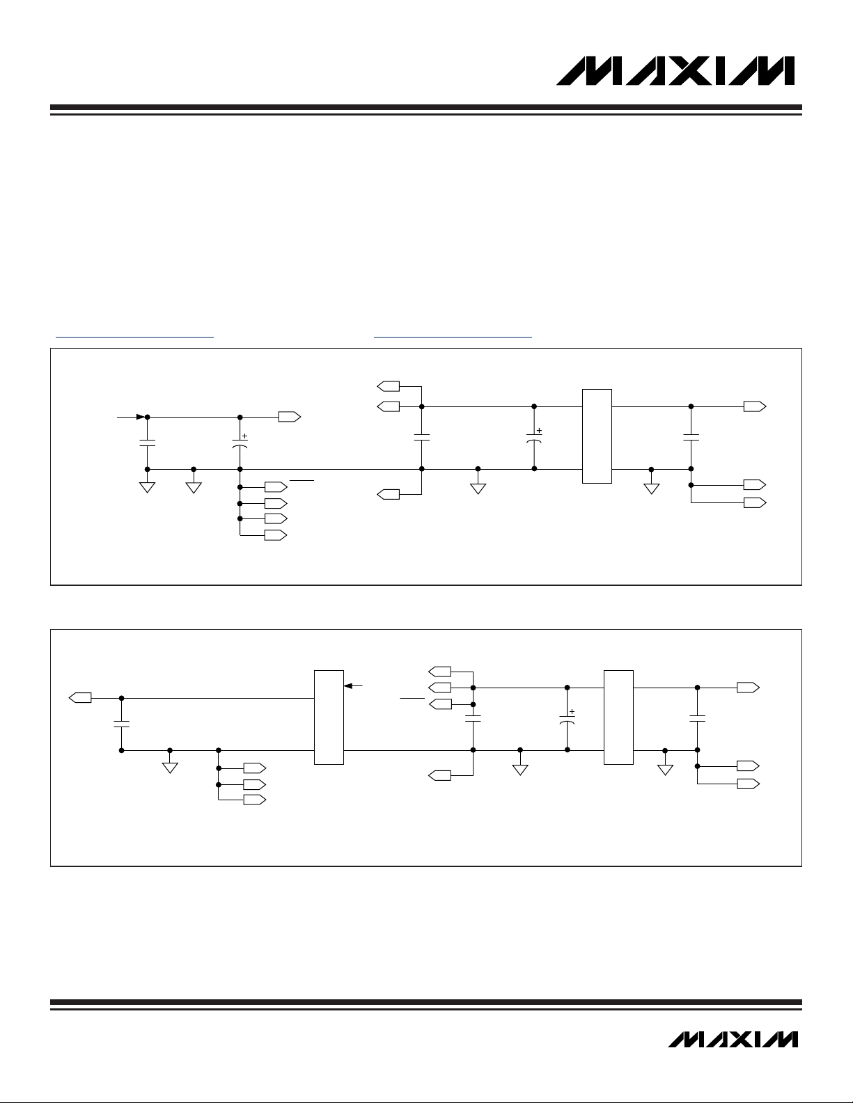
2.3 Supply Configuration
The MAXQ7665/MAXQ7666 use three supplies to power the internal analog, digital core, and digital I/O circuits. The supplies are configured as listed:
• AVDD = +5V
• DVDD = +3.3V (with internal linear regulator enabled or through an external supply)
• DVDDIO = +5V
Figure 2-2 and Figure 2-3 show the recommended supply configurations. Bypass capacitors should be mounted as close as possible
to the body of the MAXQ7665/MAXQ7666 to reduce noise. Note: If AVDD is a separate supply, no voltage monitoring is applied and
the supply voltage should not deviate more than ±300mV from DVDDIO. For PCB layout guidelines, refer to
Application Note 801
(www.maxim-ic.com/AN801) and
Application Note 637
(www.maxim-ic.com/AN637).
Figure 2-2. Supply Configuration 1 (Using Internal Linear Regulator)
Figure 2-3. Supply Configuration 2 (External DVDD)
MAXQ7665/MAXQ7666 User’s Guide
2-11 __________________________________________________________________________________________________________
DRIVEN FROM
INTERNAL LDO
(SEE NOTE)
DVDDIO
DVDDIO
DVDD
4.7μF0.1μF
0.1μF
MAIN SUPPLY
GENERATION
+5.0V
1μF
AVDD
0.1μF
REGEN
DGND
DGND
DGND
NOTE: USE A LOW-ESR CAPACITOR SIMILAR TO VISHAY TYPE 591D.
GNDIO
EXTERNAL LDO
DVDD
0.1μF
(SEE NOTE)
NOTE: USE A LOW-ESR CAPACITOR SIMILAR TO VISHAY TYPE 591D.
DGND
DGND
DGND
+3.3V
GND
+5.0V
DVDDIO
DVDDIO
REGEN
GNDIO
0.1μF
GND
MAIN SUPPLY
GENERATION
1μF
+5.0V
GND
AGND
AGND
AVDD
0.1μF
AGND
AGND
Page 84
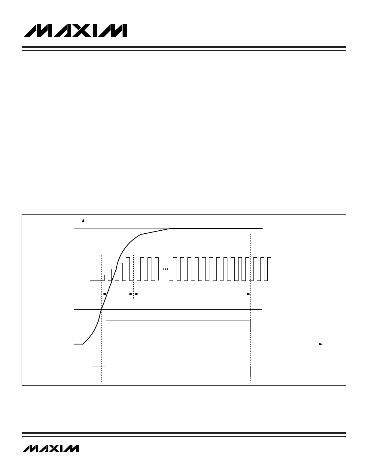
MAXQ7665/MAXQ7666 User’s Guide
__________________________________________________________________________________________________________ 2-12
2.4 Linear Regulator
The MAXQ7665/MAXQ7666 contain a +3.3V, low dropout (LDO) linear regulator. The regulator powers the MAXQ7665/MAXQ7666 digital core functions including the CPU, flash, SRAM, oscillator, and all the digital peripherals. The linear regulator is powered by the +5V
DVDDIO supply. The REGEN signal must be connected to GNDIO to enable the internal regulator. When the internal linear regulator is
disabled (REGEN connected to DVDDIO), an external +3.3V supply must be used.
2.5 Power-On Reset
The MAXQ7665/MAXQ7666 support an on-chip power-on reset (POR) circuit to ensure proper initialization of internal device states. The
POR circuit provides a power-on rising voltage threshold and a minimum power-on delay sufficient to accomplish this initialization. When
power is first applied to the MAXQ7665/MAXQ7666, the MAXQ7665/MAXQ7666 are held in a power-on reset state (Figure 2-4). The
MAXQ7665/MAXQ7666 power-on circuitry (POR) monitors the DVDD supply voltage in relation to the on-chip band gap voltage reference.
On power-up, once DVDD exceeds ~1.2V, the RESET pin is asserted to be logic-low. All the internal system and peripheral registers are
reset if DVDD from cold start exceeds ~1.2. Also, above this voltage, the power-on-reset delay counter is started.
For the MAXQ7665/MAXQ7666 to exit power-on reset, the following two conditions must apply:
• DVDD is above the power-on-reset rising voltage threshold level V
RST
(2.7V–2.99V power-on default)
• The internal RC oscillator has completed 65,536 cycles (power-on-reset delay for power supply to stabilize; about 8.6ms at 7.6MHz)
Once the power-up period has elapsed, the reset condition is removed automatically (RESET pin goes high) and software execution will
begin at the reset vector location 8000h (in the utility ROM). Software can determine whether a reset was caused by a power-on reset by
checking the POR flag in the WDCN register. This flag is set to 1 following a power-on reset, and should be cleared by software after it
has been checked.
Figure 2-4. MAXQ7665/MAXQ7666 Power-On Reset
Note: In a brownout reset (BOR) situation (see
Section 2.5.2
), where the voltage drops below the DVDD BOR threshold (e.g., 2.7V) and
rises back above the default power-on-reset rising voltage threshold level (2.7V), the POR flag in WDCN register will not be set unless
DVDD drops below ~1.2V. The POR flag will be set if DVDD voltage drops below ~1.2V and rises back above the default POR rising
voltage threshold (2.7V). In such a case, the MAXQ7665/MAXQ7666 go through a complete POR reset as described above.
NOMINAL DVDD
(+3.3V)
V
RST
(+2.7V)
INTERNAL
RC
STARTUP TIME
+1.2V
DGND
POWER-UP DELAY (65,536 RC CYCLES
OR 8.6ms AT 7.6MHz)
INTERNAL RESET
RESET PIN
Page 85

2.5.1 Power-Up Counter
An independent power-up counter functions as the startup counter to count 65,536 cycles of the internal 7.6MHz RC oscillator from initial power-on. This time period is verified by the counter after the DVDD level reaches the reset threshold (V
RST
). The counter is active
only during initial power-up and is completely shut off during normal operation.
2.5.2 DVDD Brownout Reset (BOR)
The DVDD brownout reset monitoring is enabled when the VDPE bit in the APE register is set to logic 1. The BOR circuitry monitors the
DVDD voltage and invokes a brownout reset state to halt program execution if the DVDD voltage falls in the threshold range determined by the VDBR[1:0] bits in the VMC register. The MAXQ7665/MAXQ7666 are held in the brownout reset state (Figure 2-5) while
the DVDD voltage is below the reset threshold level and the RESET pin is asserted to be logic-low. Table 2-2 shows the supported
brownout reset threshold range. When the DVDD power sources return above the threshold level, a brownout reset cycle is performed.
For the MAXQ7665/MAXQ7666 to exit brownout reset, the following condition must apply:
• DVDD is above the brownout reset threshold level determined by the VDBR[1:0] bits.
Once the above condition is satisfied, the brownout reset condition is removed automatically (RESET pin goes high) and software execution will begin at the reset vector location 8000h (in the utility ROM). A brownout reset cycle is similar to power-on reset cycle shown
in Figure 2-4, except that there is no power-up counter delay, V
RST
is determined by the VDBR[1:0] bits, and some selected register
bits are maintained and not reset to default state. For example, the VDBR1 and VDBR0 bits are only cleared by POR, not by BOR.
A brownout reset caused by a DVDD drop below the selected threshold level appears to be the same as a power-on reset, only if DVDD
voltage falls below ~1.2V and rises back above the default POR rising voltage threshold. In such a case, the MAXQ7665/MAXQ7666
go through a complete POR reset (see Figure 2-6) as described in Section 2.5 and the POR flag in the WDCN register will be set.
Note: The DVDD brownout reset monitoring is enabled (VDPE = 1) by default after all forms of reset. The VDBR1 and VDBR0 bits are
only cleared by POR (only if DVDD goes below ~1.2V in the case of BOR) and retain the selected level after all other forms of reset.
Table 2-2. DVDD Brownout Reset Threshold Range
MAXQ7665/MAXQ7666 User’s Guide
2-13 __________________________________________________________________________________________________________
* Reconfirm the values provided in this table with those in the latest MAXQ7665 and MAXQ7666 data sheets.
VDBR1:VDBR0
00 2.70–2.99 (default)
01 2.77–3.06
10 2.84–3.13
11 2.91–3.20
DVDD BROWNOUT
RESET THRESHOLD RANGE (V)*
Page 86
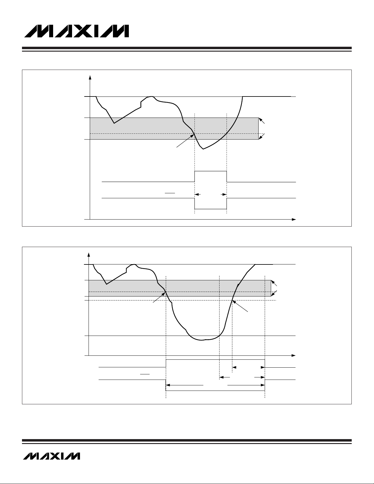
MAXQ7665/MAXQ7666 User’s Guide
__________________________________________________________________________________________________________ 2-14
Figure 2-5. MAXQ7665/MAXQ7666 Brownout Reset
NOMINAL
Figure 2-6. MAXQ7665/MAXQ7666 Brownout/Power-On Reset
DVDD (+3.3V)
+3.06V
+2.77V
DGND
NOMINAL
DVDD (+3.3V)
+3.06V
+2.77V
+2.70V
BROWNOUT RESET
BROWNOUT RESET
INTERNAL RESET
RESET PIN
DVDD BROWNOUT RESET
THRESHOLD RANGE
VDBR[1:0] = 01
BOR STATE
DVDD BROWNOUT RESET
THRESHOLD RANGE
VDBR[1:0] = 01
DEFAULT BOR
THRESHOLD
~ +1.20V
DGND
INTERNAL RESET
RESET PIN
POWER-UP
DELAY
POR STATE
BOR STATE
Page 87

2.5.3 Reset Output
The MAXQ7665/MAXQ7666 assert the RESET signal during power-up and also during reset conditions caused by an internal source
(such as brownout, watchdog, or internal reset). On power-up, once DVDD exceeds 1.2V, RESET is asserted to be logic-low. As DVDD
rises, RESET remains low. When DVDD exceeds the default BOR threshold, RESET is kept low until the internal RC oscillator has completed 65,536 cycles; after this period, if DVDD remains above the default BOR threshold, RESET goes high. If a brownout reset condition occurs, RESET is asserted low. Each time a DVDD BOR reset is triggered, it stays low until DVDD exceeds the BOR reset threshold.
Note: The RESET pin is an output and an input. The MAXQ7665/MAXQ7666 is placed into an external reset mode if the RESET pin is
held low for at least four clock cycles. See
Section 2.7.2
for more information on external reset.
2.6 Power-Supply Voltage Monitors
The MAXQ7665/MAXQ7666 contain two power-supply voltage monitors that can be used to continually monitor the DVDD and DVDDIO
supply voltages for brownout conditions and initiate interrupt requests if enabled. The DVDD and DVDDIO voltage monitors can be independently activated by programming the corresponding enable bits (VDBE and VIBE) in the analog power-enable (APE) register.
2.6.1 Digital Core Supply (DVDD) Monitor
The digital core supply monitor detects a brownout condition on the +3.3V DVDD supply. The DVDD supply monitor can be independently activated by programming the corresponding enable bit (VDBE) in the analog power enable (APE) register. A brownout is detected when the DVDD supply voltage drops below the programmed brownout detection threshold (Figure 2-7). The brownout interrupt
threshold level is user selectable, and can be programmed using the brownout interrupt threshold bits (VDBI[1:0]) in the VMC register. The supported threshold levels are listed in Table 2-3. If enabled, a DVDD brownout interrupt can be generated that allows for saving data and the present state of the MAXQ7665/MAXQ7666. A DVDD brownout interrupt is generated only if the interrupt enable bit
(DVBIE) in the analog interrupt enable (AIE) register is set. Also, global interrupt mask bits IM5 (in the IMR register) and IGE in (the IC
register) must be enabled.
If the DVDD supply falls further, then the brownout reset threshold is tripped, terminating program operation and holding the
MAXQ7665/MAXQ7666 in the brownout reset state. The MAXQ7665/MAXQ7666 remain in the brownout reset state until the supply rises
above the reset threshold. The DVDD monitor brownout interrupt and reset trip points can differ from device to device within the programmed threshold range. This tolerance error is caused by the monitor comparator offsets, and threshold setting circuitry. The
brownout interrupt and reset thresholds will track each other to some degree. If the brownout interrupt trip point is trending towards the
lower side of the threshold level, then the brownout reset trip point will also trend towards the lower side of the threshold level. The
brownout reset is always below the brownout interrupt threshold for equivalent settings, ensuring adequate notice of a failing supply
condition.
Table 2-3. DVDD Brownout Interrupt Threshold Range
MAXQ7665/MAXQ7666 User’s Guide
2-15 __________________________________________________________________________________________________________
* Reconfirm the values provided in this table with those in the latest MAXQ7665 and MAXQ7666 data sheets.
VDBI[1:0] DVDD (CORE) (V)*
00 (default) 2.77–2.99
01 2.84–3.13
10 2.91–3.20
11 2.99–3.27
Page 88
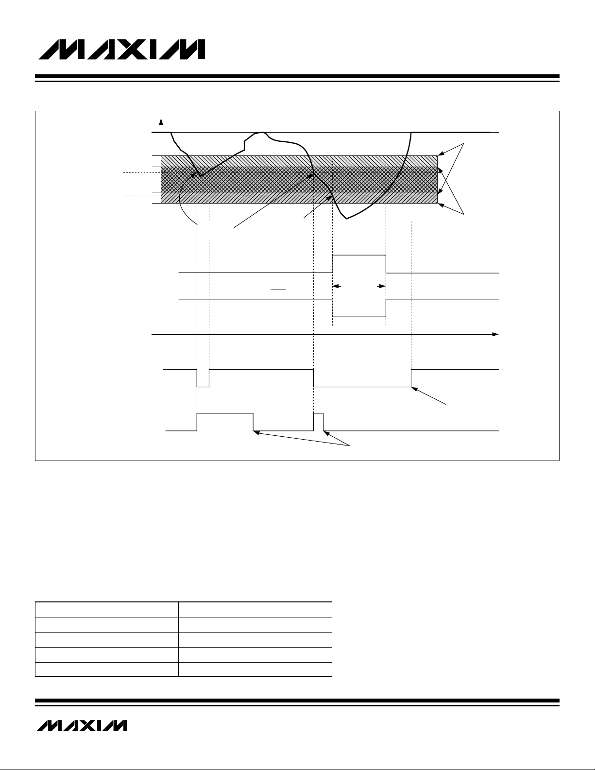
MAXQ7665/MAXQ7666 User’s Guide
__________________________________________________________________________________________________________ 2-16
Figure 2-7. DVDD Brownout Interrupt Threshold Detection
BROWNOUT
2.6.2 Digital I/O Supply (DVDDIO) Monitor
The DVDDIO monitor detects a brownout condition on the +5V digital I/O supply. The DVDDIO supply monitor can be independently
activated by programming the corresponding enable bit (VIBE) in the APE register. A brownout is detected when the DVDDIO supply
voltage falls in the programmed DVDDIO brownout detection threshold range (Figure 2-8). The brownout interrupt threshold range is
user selectable, and can be programmed using the brownout interrupt threshold bits (VIOBI[1:0]) in the VMC register. The supported
threshold range are listed in Table 2-4. If enabled, an interrupt can be generated that allows for saving data and the present state of
the MAXQ7665/MAXQ7666. A DVDDIO brownout interrupt is generated only if the interrupt enable bit (VIOBIE) in the AIE register is
set. Also, global interrupt mask bits IM5 (in the IMR register) and IGE in (the IC register) must be enabled.
Table 2-4. DVDDIO Brownout Interrupt Threshold Range
* Reconfirm the values provided in this table with those in the latest MAXQ7665 and MAXQ7666 data sheets.
INTERRUPT TRIGGER
POINT
BROWNOUT
RESET TRIGGER
POINT
NOMINAL
DVDD (+3.3V)
+3.13V
+3.06V
+2.84V
+2.77V
BROWNOUT
INTERRUPT
DVDD BROWNOUT
INTERRUPT
THRESHOLD RANGE
VDBI[1:0] = 01
DVDD BROWNOUT
RESET THRESHOLD
BROWNOUT
RESET
INTERNAL RESET
RANGE VDBR[1:0] = 01
RESET OUTPUT
DGND
DVLVL FLAG
(ASR[14])
DVBI FLAG
(ASR[4])
BOR STATE
VDBE BIT SET BY μC
FLAG ARBITRARILY
CLEARED BY μC
VIOBI[1:0] DVDDIO (V)*
00 (default) 4.25–4.74
01 4.30–4.79
10 4.35–4.84
11 4.40–4.89
Page 89
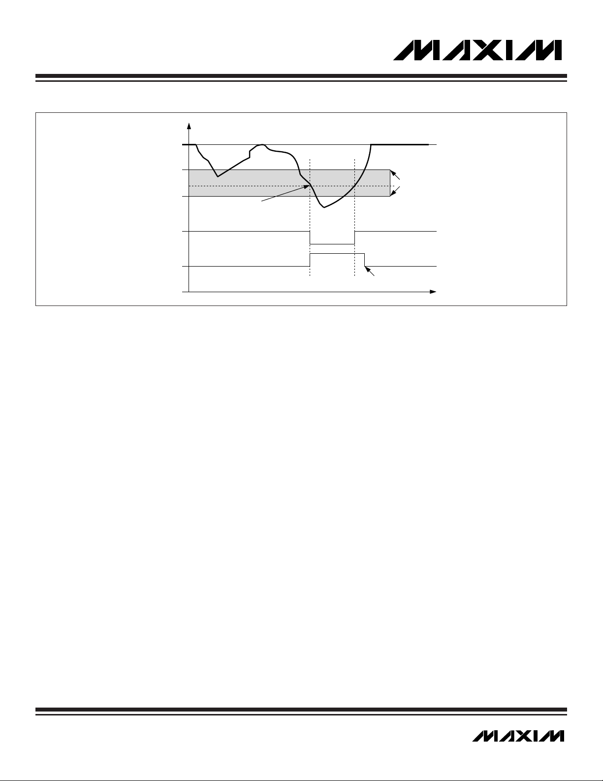
Figure 2-8. DVDDIO Brownout Interrupt Threshold Detection
2.7 Reset Mode
When the MAXQ7665/MAXQ7666 are in reset mode, the enabled system clock oscillator continues running, but no instruction execution or other system or peripheral operations occur, and all input/output pins return to default states. Once the condition that caused
the reset (whether internal or external) is removed, code execution resumes at address 8000h for all reset types. Some of the reset
sources will also trigger a delaying count of 65,536 clocks (as discussed above) before execution starts.
There are five different sources that can cause the MAXQ7665/MAXQ7666 to enter reset mode. See
Section 2.5
for information on
power-on and brownout reset.
• Power-on reset
• Brownout reset
• Watchdog timer reset
• External reset
• Internal system reset
2.7.1 Watchdog Timer Reset
The MAXQ7665/MAXQ7666 watchdog timer is described in
Section 5
. The watchdog timer is a programmable hardware timer that can
be set to reset the MAXQ7665/MAXQ7666 in the case of a software lockup or other unrecoverable error. Once the watchdog is enabled
in this manner, the processor must refresh the watchdog periodically to avoid a reset. If the processor does not reset the watchdog timer
before it elapses, the watchdog will initiate a reset state. When running at 7.6MHz, the maximum watchdog time period before reset is
approximately 276ms.
If the watchdog resets the MAXQ7665/MAXQ7666, it remains in reset and holds the RESET pin low for four clock cycles. Once the reset
condition has completed, the processor will begin executing program code at address 8000h. When a reset occurs due to a watchdog timeout, the watchdog timer reset flag in the WDCN register is set to 1 and can only be cleared by software. User software can
examine this bit following a reset to determine if that reset was caused by a watchdog timeout.
Since the XT bit in the CKCN register and the HFE bit in the OSCC register are cleared to 0 only on power-on reset, it is possible to
exit a watchdog reset with the clock source set to the high frequency crystal oscillator. In this case, execution resumes running from
the RC oscillator, and the switchover to the high-frequency oscillator occurs automatically when the crystal oscillator is ready.
MAXQ7665/MAXQ7666 User’s Guide
2-17 __________________________________________________________________________________________________________
NOMINAL
DVDDIO (+5.0V)
+4.79V
+4.30V
VIOLVL
FLAG
VIOBI
FLAG
GNDIO
DVDDIO
BROWNOUT
INTERRUPT
VIOBI FLAG CLEARED
IN INTERRUPT HANDLER
DVDDIO BROWNOUT
INTERRUPT THRESHOLD
RANGE VIOBI[1:0] = 01
Page 90

2.7.2 External Reset
During normal operation, the MAXQ7665/MAXQ7666 devices are placed into an external reset mode by holding the RESET pin low for
at least four clock cycles. If the MAXQ7665/MAXQ7666 devices are in the low-power stop mode (i.e., system clock is not active), the
RESET pin becomes an asynchronous source, forcing the reset state immediately after being taken to logic 0. Once the MAXQ7665/
MAXQ7666 enter reset mode, it remains in reset as long as the RESET pin is held at logic 0. After the RESET pin returns to logic 1, the
processor starts the internal 7.6MHz RC oscillator if necessary and exits the reset state within four clock cycles (Figure 2-9) and begins
program execution at address 8000h.
The RESET pin is an output and an input. If a reset condition is caused by an internal source (such as a brownout reset, watchdog, or
internal reset), an output reset pulse or low level is generated at the RESET pin as long as the MAXQ7665/MAXQ7666 remain in reset.
If the RESET pin is connected to an incompatible external reset circuit, it may not be able to drive the output reset signal. However, if
this occurs it does not affect the internal reset condition.
Because the XT bit in the CKCN register and the HFE bit in the OSCC register are cleared to 0 only on power-on reset, it is possible to
exit an external reset with the clock source set to the high-frequency crystal oscillator. In this case, execution resumes running from
the RC oscillator, and the switchover to the high-frequency oscillator occurs automatically when the crystal oscillator is ready.
2.7.3 Internal System Reset
The MAXQ7665/MAXQ7666 support internal system reset capability from in-system programming mode. An internal system reset is
generated when the ROD bit in the system control register is set. The SPE bit in the ICDF register must also be set. The bootloader
software can use this capability to initiate an internal system reset when the flash loader completes its operation. See
Section 12
for
more details on in-system programming.
MAXQ7665/MAXQ7666 User’s Guide
__________________________________________________________________________________________________________ 2-18
Figure 2-9. MAXQ7665/MAXQ7666 External Reset
SYSTEM CLOCK
RESET
RESET
SAMPLING
INTERNAL
RESET
FIRST
INSTRUCTION
FETCH
Page 91

MAXQ7665/MAXQ7666 User’s Guide
___________________________________________________________________________________
Maxim Integrated Products
3-1
SECTION 3: ANALOG I/O MODULE
This section contains the following information:
3.1 Architecture . . . . . . . . . . . . . . . . . . . . . . . . . . . . . . . . . . . . . . . . . . . . . . . . . . . . . . . . . . . . . . .3-5
3.1.1 Analog I/O Pins . . . . . . . . . . . . . . . . . . . . . . . . . . . . . . . . . . . . . . . . . . . . . . . . . . . . . . .3-6
3.2 Analog I/O Module Control and Status Registers . . . . . . . . . . . . . . . . . . . . . . . . . . . . . . . . . .3-7
3.2.1 Analog Power Enable Register (APE) . . . . . . . . . . . . . . . . . . . . . . . . . . . . . . . . . . . . .3-7
3.2.2 ADC Control Register (ACNT) . . . . . . . . . . . . . . . . . . . . . . . . . . . . . . . . . . . . . . . . . . .3-8
3.2.3 DAC Control Register (DCNT) . . . . . . . . . . . . . . . . . . . . . . . . . . . . . . . . . . . . . . . . . . .3-11
3.2.4 DAC Input Data Register (DACI) . . . . . . . . . . . . . . . . . . . . . . . . . . . . . . . . . . . . . . . . .3-12
3.2.5 DAC Output Data Register (DACO) . . . . . . . . . . . . . . . . . . . . . . . . . . . . . . . . . . . . . . .3-12
3.2.6 ADC Data Register (ADCD) . . . . . . . . . . . . . . . . . . . . . . . . . . . . . . . . . . . . . . . . . . . . .3-13
3.2.7 Temperature Sense Offset Register (TSO) . . . . . . . . . . . . . . . . . . . . . . . . . . . . . . . . . .3-13
3.2.8 Analog Interrupt Enable Register (AIE) . . . . . . . . . . . . . . . . . . . . . . . . . . . . . . . . . . . .3-14
3.2.9 Analog Status Register (ASR) . . . . . . . . . . . . . . . . . . . . . . . . . . . . . . . . . . . . . . . . . . . .3-15
3.2.10 Oscillator Control Register (OSCC) . . . . . . . . . . . . . . . . . . . . . . . . . . . . . . . . . . . . . .3-16
3.3 Analog-to-Digital Converter (ADC) Port . . . . . . . . . . . . . . . . . . . . . . . . . . . . . . . . . . . . . . . . . .3-17
3.3.1 ADC Signals . . . . . . . . . . . . . . . . . . . . . . . . . . . . . . . . . . . . . . . . . . . . . . . . . . . . . . . . .3-18
3.3.2 Differential Inputs . . . . . . . . . . . . . . . . . . . . . . . . . . . . . . . . . . . . . . . . . . . . . . . . . . . . .3-18
3.3.3 True-Differential Analog Input T/H . . . . . . . . . . . . . . . . . . . . . . . . . . . . . . . . . . . . . . . .3-20
3.3.4 Unipolar/Bipolar . . . . . . . . . . . . . . . . . . . . . . . . . . . . . . . . . . . . . . . . . . . . . . . . . . . . . .3-21
3.3.5 Transfer Function . . . . . . . . . . . . . . . . . . . . . . . . . . . . . . . . . . . . . . . . . . . . . . . . . . . . .3-22
3.3.6 Programmable Gain Amplifier . . . . . . . . . . . . . . . . . . . . . . . . . . . . . . . . . . . . . . . . . . .3-25
3.3.7 Analog Input Protection . . . . . . . . . . . . . . . . . . . . . . . . . . . . . . . . . . . . . . . . . . . . . . . .3-26
3.3.8 ADC Clock . . . . . . . . . . . . . . . . . . . . . . . . . . . . . . . . . . . . . . . . . . . . . . . . . . . . . . . . . .3-27
3.3.9 Auto Shutdown Mode . . . . . . . . . . . . . . . . . . . . . . . . . . . . . . . . . . . . . . . . . . . . . . . . . .3-27
3.3.10 ADC Conversion Start Sources and Timing . . . . . . . . . . . . . . . . . . . . . . . . . . . . . . . .3-28
3.3.11 ADC Interrupts . . . . . . . . . . . . . . . . . . . . . . . . . . . . . . . . . . . . . . . . . . . . . . . . . . . . . .3-32
3.3.12 Using the ADC . . . . . . . . . . . . . . . . . . . . . . . . . . . . . . . . . . . . . . . . . . . . . . . . . . . . . .3-33
Page 92

3.4 Temperature Sensor . . . . . . . . . . . . . . . . . . . . . . . . . . . . . . . . . . . . . . . . . . . . . . . . . . . . . . . . .3-34
3.4.1 Temperature Sensor Signals. . . . . . . . . . . . . . . . . . . . . . . . . . . . . . . . . . . . . . . . . . . . . 3-35
3.4.2 Using the Temperature Sensor . . . . . . . . . . . . . . . . . . . . . . . . . . . . . . . . . . . . . . . . . . . 3-35
3.4.3 Internal Temperature Sensor . . . . . . . . . . . . . . . . . . . . . . . . . . . . . . . . . . . . . . . . . . . . 3-36
3.4.4 Remote Temperature Sensor Driver . . . . . . . . . . . . . . . . . . . . . . . . . . . . . . . . . . . . . . . 3-36
3.4.4.1 Differential Temperature Measurement . . . . . . . . . . . . . . . . . . . . . . . . . . . . . . .3-37
3.4.4.2 Single-Ended Temperature Measurement . . . . . . . . . . . . . . . . . . . . . . . . . . . . .3-37
3.4.5 Remote Temperature Sensor Selection . . . . . . . . . . . . . . . . . . . . . . . . . . . . . . . . . . . .3-37
3.5 Digital-to-Analog Converter (DAC) Port . . . . . . . . . . . . . . . . . . . . . . . . . . . . . . . . . . . . . . . . . .3-37
3.5.1 DAC Signals . . . . . . . . . . . . . . . . . . . . . . . . . . . . . . . . . . . . . . . . . . . . . . . . . . . . . . . . . 3-38
3.5.2 External Reference Input and Output Buffer . . . . . . . . . . . . . . . . . . . . . . . . . . . . . . . . 3-38
3.5.3 Loading DAC Data Register for Conversion . . . . . . . . . . . . . . . . . . . . . . . . . . . . . . . . 3-39
3.5.4 DAC Power-Down . . . . . . . . . . . . . . . . . . . . . . . . . . . . . . . . . . . . . . . . . . . . . . . . . . . . . 3-40
3.5.5 Using the DAC . . . . . . . . . . . . . . . . . . . . . . . . . . . . . . . . . . . . . . . . . . . . . . . . . . . . . . . 3-40
MAXQ7665/MAXQ7666 User’s Guide
___________________________________________________________________________________________________________ 3-2
Page 93

MAXQ7665/MAXQ7666 User’s Guide
3-3 ___________________________________________________________________________________________________________
Figure 3-1. Analog I/O Module Block Diagram . . . . . . . . . . . . . . . . . . . . . . . . . . . . . . . . . . . . . . .3-5
Figure 3-2. Differential Input ADC Block Diagram . . . . . . . . . . . . . . . . . . . . . . . . . . . . . . . . . . . . .3-17
Figure 3-3. Multiplexer Input Connection Scheme . . . . . . . . . . . . . . . . . . . . . . . . . . . . . . . . . . . . .3-19
Figure 3-4A. Equivalent Input Circuit (Acquisition Mode with PGA Bypassed) . . . . . . . . . . . . . .3-21
Figure 3-4B. Equivalent Input Circuit (Hold/Conversion Mode with PGA Bypassed) . . . . . . . . . .3-21
Figure 3-5. Unipolar Transfer Function (PGA Gain = 1) . . . . . . . . . . . . . . . . . . . . . . . . . . . . . . . . .3-22
Figure 3-6. Bipolar Transfer Function (PGA Gain = 1) . . . . . . . . . . . . . . . . . . . . . . . . . . . . . . . . . .3-23
Figure 3-7. PGA Block Diagram . . . . . . . . . . . . . . . . . . . . . . . . . . . . . . . . . . . . . . . . . . . . . . . . . . .3-25
Figure 3-8. Analog Input Range Measuring a Positive Analog Input Value . . . . . . . . . . . . . . . . .3-26
Figure 3-9. Analog Input Range Measuring a Negative Analog Input Value . . . . . . . . . . . . . . . .3-27
Figure 3-10. Single-Edge ADC Conversion Timing; ADC Previously Off and PGA Bypassed . . .3-31
Figure 3-11. Single-Edge ADC Conversion Timing; ADC Previously On and PGA Bypassed . . .3-31
Figure 3-12. Dual-Edge ADC Conversion Timing; ADC Previously Off and PGA > 1 . . . . . . . . . .3-32
Figure 3-13. Flow Chart for Initializing and Using the ADC . . . . . . . . . . . . . . . . . . . . . . . . . . . . . .3-33
Figure 3-14. MAXQ7665/MAXQ7666 Temperature Sensor Block Diagram . . . . . . . . . . . . . . . . . .3-34
Figure 3-15. Temperature Transfer Function . . . . . . . . . . . . . . . . . . . . . . . . . . . . . . . . . . . . . . . . .3-36
Figure 3-16. DAC Block Diagram . . . . . . . . . . . . . . . . . . . . . . . . . . . . . . . . . . . . . . . . . . . . . . . . . .3-38
LIST OF FIGURES
Page 94

MAXQ7665/MAXQ7666 User’s Guide
___________________________________________________________________________________________________________ 3-4
Table 3-1. Analog I/O Module Signals . . . . . . . . . . . . . . . . . . . . . . . . . . . . . . . . . . . . . . . . . . . . . .3-6
Table 3-2. ADC Signals . . . . . . . . . . . . . . . . . . . . . . . . . . . . . . . . . . . . . . . . . . . . . . . . . . . . . . . . .3-18
Table 3-3. PGA Gain and Channel Input Capacitance . . . . . . . . . . . . . . . . . . . . . . . . . . . . . . . . .3-20
Table 3-4. Unipolar Code Table (PGA Gain = 1) . . . . . . . . . . . . . . . . . . . . . . . . . . . . . . . . . . . . . .3-22
Table 3-5. Unipolar Input Scaling . . . . . . . . . . . . . . . . . . . . . . . . . . . . . . . . . . . . . . . . . . . . . . . . . .3-23
Table 3-6. Bipolar Code Table (PGA Gain = 1) . . . . . . . . . . . . . . . . . . . . . . . . . . . . . . . . . . . . . . .3-24
Table 3-7. Bipolar Input Scaling . . . . . . . . . . . . . . . . . . . . . . . . . . . . . . . . . . . . . . . . . . . . . . . . . . .3-24
Table 3-8. ADC Conversion Start Source Selection . . . . . . . . . . . . . . . . . . . . . . . . . . . . . . . . . . . .3-28
Table 3-9. ADC Dual- and Single-Edge Modes . . . . . . . . . . . . . . . . . . . . . . . . . . . . . . . . . . . . . . .3-29
Table 3-10. Temperature Sensor Signals . . . . . . . . . . . . . . . . . . . . . . . . . . . . . . . . . . . . . . . . . . . .3-35
Table 3-11. Remote Sensor Transistor Manufacturers . . . . . . . . . . . . . . . . . . . . . . . . . . . . . . . . . .3-37
Table 3-12. DAC Signals . . . . . . . . . . . . . . . . . . . . . . . . . . . . . . . . . . . . . . . . . . . . . . . . . . . . . . . .3-38
Table 3-13. DAC Input Code to Output Voltage (Gain = 1) . . . . . . . . . . . . . . . . . . . . . . . . . . . . . .3-39
Table 3-14. DAC Load Control Selection . . . . . . . . . . . . . . . . . . . . . . . . . . . . . . . . . . . . . . . . . . . .3-39
LIST OF TABLES
Page 95

SECTION 3: ANALOG I/O MODULE
The MAXQ7665/MAXQ7666 contain an ultra-low-power precision analog I/O module for measuring and controlling a host of sensors,
motors, bridges, and other analog peripherals. The analog I/O module has all the components to make the MAXQ7665/MAXQ7666
stand-alone data-acquisition machines ideal for harsh environment applications. Except where explicitly noted, the MAXQ7665 and
MAXQ7666 support identical features.
The analog I/O module includes the following features:
• 8 differential analog-input multiplexer
• Low-power, 12-bit, 500ksps successive approximation ADC
• 12-bit, buffered, voltage-output DAC
• On-chip ±1°C accurate temperature sensor (typ)
• Remote temperature sensor drive circuit
• Internal programmable gain amplifier (x1, x2, x4, x8, x16, x32)
• Individual external reference inputs for the ADC and DAC
3.1 Architecture
The analog-input multiplexer supports 8 differential measurements and feeds the programmable gain amplifier (PGA) and the 12-bit
SAR ADC. The low noise, programmable gain amplifier with gains of x1 to x32 allows interfacing to a variety of devices with different
signal amplitudes. The ADC conversion clock source is the same as the system clock source (internal oscillator or external
crystal/clock) and has a user-programmable clock division ratio. The 12-bit voltage-out DAC has internal feedback resistors for reducing external component count. The internal temperature sensor performs temperature measurements with an internal diode-connected transistor. In the remote temperature sensor drive configuration, the device provides the proper bias necessary to measure temperature with up to two external diode-connected transistor sensors. The MAXQ7665/MAXQ7666 support independent external reference inputs for the ADC and DAC to allow the use of high precision, high quality reference sources.
Figure 3-1 shows a functional block diagram of the MAXQ7665/MAXQ7666 analog I/O module.
MAXQ7665/MAXQ7666 User’s Guide
3-5 ___________________________________________________________________________________________________________
Figure 3-1. Analog I/O Module Block Diagram
AIN15
AIN14
AIN13
AIN12
AIN11
AIN10
AIN9
AIN8
AIN7
AIN6
AIN5
AIN4
AIN3
AIN2
AIN1
AIN0
INTERNAL
TEMP
SENSOR
TSE
8 DIFFERENTIAL
CHANNEL
MULTIPLEXER
ANALOG I/O FUNCTIONAL BLOCKS
REFADC
P0.4/
ADCCNV
PGA
PGAE
PGG[2:0]
ADCASD
ADCDIFADCMX[4:0]
12-BIT
500kHz
ADC
ADCSADCE
ADCBIP
ADCBY ADCDUL
DATA BUS (15:0)
REFDAC
12-BIT
DAC
DACE
P0.5/
DACLOAD
ADCCLK
TIMER 2
TIMER 1
TIMER 0
VDAC
50kΩ
50kΩ
Page 96

3.1.1 Analog I/O Pins
The analog I/O module has 24 pins associated with the analog functions on the microcontroller. Table 3-1 shows the external interface
signals used by the analog I/O module.
Table 3-1. Analog I/O Module Signals
MAXQ7665/MAXQ7666 User’s Guide
___________________________________________________________________________________________________________ 3-6
SIGNAL FUNCTION
AIN15
AIN14
AIN13
AIN12
AIN11
AIN10
AIN9
AIN8
AIN7
AIN6
AIN5
AIN4
AIN3
AIN1
AIN2/TS2
AIN0/TS0
DACOUT
P0.4/ADCCNV
P0.5/DACLOAD
REFADC
REFDAC
AVDD
AGND Analog Ground (2 pins)
EP
ADC Analog Input #. These are dedicated analog input pins connected through the internal analog multiplexer to the PGA and ADC.
The analog multiplexer supports 8 differential- input measurements. In differential-input mode, the inputs are paired: AIN14 to
AIN15, AIN12 to AIN13, AIN10 to AIN11, AIN8 to AIN9, AIN6 to AIN7, AIN4 to AIN5, AIN2 to AIN3, AIN0 to AIN1.
ADC Analog Input/Remote Temperature Sensor. Analog input pins AIN2 and AIN0 are shared with the remote temperature-sensor
dr ive line. If the remote temperature-sensor drive circuit is not selected, the pin can be used as a differential input to the
multiplexer. In differential-input configuration, AIN2 is referenced to AIN3 while AIN0 is referenced to AIN1. When selected, the
remote temperature-sensor drive circuit supplies suitable current to drive an external diode-connected transistor to monitor
temperature away from the microcontroller. The remote temperature measurement can be made either in single-ended or
differential configuration. Note: In differential configuration, AIN3 is used as the return path for AIN2 and AIN1 is used as the return
path for AIN0.
DAC Voltage Output. DACOUT is a dedicated output pin. If the DAC is disabled, the pin is configured as a 100k pulldown
res istor to AGND. The DACOUT line can be used for precis ion drive applications.
ADC Convers ion Start Input/Port 0 Data Bit 4. The ADC convers ion start is a shared pin w ith the general-purpose digital I/O port 0
bit 4. As ADCCNV, this pin can trigger ADC sampling and conversion on a rising or falling edge. After power-up or a reset this
pin defaults to a digital I/O port pin w ith pullup enabled.
DAC Load Input/Port 0 Data Bit 5. The DAC load is a shared pin with the general-purpose digital I/O port 0 bit 5. As DACLOAD,
this pin can trigger DAC conversion by loading the DAC output register on a rising or falling edge. After power-up or a reset this
pin defaults to a digital I/O port pin with pullup enabled.
ADC Reference Input. The REFADC input pin is used to supply an external precision voltage reference to the AD C. The REFADC
can handle a voltage range from 1V to AVDD. The REFADC input determines the full-scale range (FSR) of the internal 12-bit ADC.
DAC Reference Input. The REFDAC input pin is used to supply an external precision voltage reference to the DAC. The REFDAC
can handle a voltage range from 0 to AVDD . The REFDAC input determine the full-scale range (FSR) of the internal 12-bit DAC.
Analog V
Exposed Paddle. The MAXQ7665/MAXQ7666 TQFN package has an exposed paddle on the bottom of the package, providing a
very low thermal resistance path for heat removal from the IC, as well as low-inductance path to ground. The pad is electrically
connected to AGND and should be soldered to the circuit board analog ground plane for proper thermal and electrical
performance. Refer to Maxim ’s Application Note HFAN-08.1: Thermal Considerations for QFN and Other Exposed Pad Packages
for additional infor mation.
Supply. The analog supply voltage is +5.0V for the MAXQ7665/MAXQ7666.
DD
Page 97
3.2 Analog I/O Module Control and Status Registers
The analog I/O module uses the following control and status registers.
3.2.1 Analog Power Enable Register (APE)
Register Description: Analog Power Enable Register
Register Name: APE
Register Address: Module 05h, Index 01h
Bits 15, 14, 13, 9, 8, and 2: Reserved. Read 0, write ignored.
Bit 12: I/O Voltage Brownout Detection Enable (VIBE). See
Section 2
for details on this bit.
Bit 11: Digital Voltage Brownout Detection Enable (VDBE). See
Section 2
for details on this bit.
Bit 10: Digital Voltage Reset Enable (VDPE). See
Section 2
for details on this bit.
Bits 7, 6, 5: PGA Gain Setting Bits 2, 1, 0 (PGG2, PGG1, PGG0). These bits set the PGA gain as shown in the following table. The
PGA is bypassed when the PGA gain selected is 1.
Bit 4: Temperature Sensor Enable (TSE). Setting this bit to logic 1 enables the temperature sensor. Clearing this bit to logic 0 turns
off the power to the temperature sensor and disables its operation. The ADCMX4:ADCMX0 bits in the ADC control register determine
if the internal or external temperature sensor configuration is used.
Bit 3: PGA Enable (PGAE). The PGA is enabled when this bit is set to logic 1. Clearing this bit to 0 disables the PGA. The PGAE should
be enabled 5µs before attempting a conversion with a PGA gain other than 1. Note: To bypass the PGA, select a PGA gain of 1
(PGG2:PGG0) and clear the PGAE bit to 0. Setting PGAE = 0 significantly reduces power consumption.
Bit 1: DAC Enable (DACE). Setting this bit to logic 1 enables the DAC block to be ready for conversion. Clearing this bit to logic 0
turns off the power to the DAC block and disables its operation.
Bit 0: ADC Enable (ADCE). Setting this bit to logic 1 enables the ADC block to be ready for conversion. Clearing this bit to logic 0
turns off the power to the ADC block and disables its operation.
MAXQ7665/MAXQ7666 User’s Guide
3-7 ___________________________________________________________________________________________________________
r = read, w = write
Note: This register is cleared to 0400h on all forms of reset.
Bit #
Name — — — VIBE VDBE VDPE — —
Reset 0 0 0 0 0 1 0 0
Access r r r rw rw rw r r
Bit #
Name PGG2 PGG1 PGG0 TSE PGAE — DACE ADCE
Reset 0 0 0 0 0 0 0 0
Access rw rw rw rw rw r rw rw
15 14 13 12 11 10 9 8
7 6 5 4 3 2 1 0
PGG2:PGG0 PGA GAIN
000 1 (Default)
001 2
010 4
011 8
100 16
101 32
110 Reserved, should not be used
111 Reserved, should not be used
Page 98

3.2.2 ADC Control Register (ACNT)
Register Description: ADC Control Register
Register Name: ACNT
Register Address: Module 05h, Index 02h
Bits 15 to 11: ADC Input Multiplexer Bits 4 to 0 (ADCMX4 to ADCMX0). These multiplexer bits select the inputs to the ADC and control the state of the temperature sensor.
MAXQ7665/MAXQ7666 User’s Guide
___________________________________________________________________________________________________________ 3-8
r = read, w = write
Note: This register is cleared to 0000h on all forms of reset.
Bit #
Name ADCMX4 ADCMX3 ADCMX2 ADCMX1 ADCMX0 ADCDIF ADCBIP —
Reset 0 0 0 0 0 0 0 0
Access rw rw rw rw rw rw rw r
Bit #
Name — ADCDUL — ADCASD ADCBY ADCS2 ADCS1 ADCS0
Reset 0 0 0 0 0 0 0 0
Access r rw r rw rw rw rw rw
15 14 13 12 11 10 9 8
76543210
ADCMX4:ADCMX0
00000 AIN0 AIN1 Voltage
00001 AIN1 AIN1 Offset Voltage
00010 AIN2 AIN3 Voltage
00011 AIN3 AIN3 Offset Voltage
00100 AIN4 AIN5 Voltage
00101 AIN5 AIN5 Offset Voltage
00110 AIN6 AIN7 Voltage
00111 AIN7 AIN7 Offset Voltage
01000 AIN8 AIN9 Voltage
01001 AIN9 AIN9 Offset Voltage
01010 AIN10 AIN11 Voltage
01011 AIN11 AIN11 Offset Voltage
01100 AIN12 AIN13 Voltage
01101 AIN13 AIN13 Offset Voltage
01110 AIN14 AIN15 Voltage
01111 AIN15 AIN15 Offset Voltage
1x00x Internal Internal Internal Temperature
1x01x AIN0 AIN1 Remote Temperature 1
1x10x AIN2 AIN3 Remote Temperature 2
11110 — — Reserv ed
11111 — — Reserv ed
POSITIVE NEGATIVE
ADCDIF = 1
MEASU RE
Page 99
When ADCMX4 is cleared, the ADC input channel is configured for a differential voltage measurement. When ADCMX0 is set, the ADC’s
positive and negative inputs are internally connected to the same analog input pin so the user can measure zero offset error, if any.
When ADCMX4 is set, the ADC input channel is configured to measure remote or internal temperature, and the bits ADCMX3:ADCMX0
control the temperature measurement.
The bits ADCMX1 and ADCMX2 determine if internal or external temperature sense mode is selected.
The bits ADCMX0 and ADCMX3 determine the state of the temperature sensor when measuring temperature.
ADCMX0: TS Auto-Zero Control. This bit puts the temperature sensor in auto-zero state when it is set to logic 1. The auto-zeroing is used to cancel internal offset effects.
ADCMX3: TS Current Control. This bit sets the temperature sensor current to its high value when set to logic 1, and sets the current to its low value when cleared to logic 0.
The ADC performs temperature measurement by measuring the voltage across a diode-connected transistor at two different current
levels.
Note: The temperature measurement process is fully automated in the MAXQ7665/MAXQ7666 ROM utility routine "tempConv." All the
required setup and temperature measurement algorithm steps for both internal and external temperature measurements are handled
in the utility routine and it returns the local or remote temperature result.
Bit 10: Differential Input (ADCDIF). The ADC operates only on differential inputs and this bit must be set to logic 1 if the remote or
internal temperature sensor drive circuit is not selected. For the remote temperature sensor, this bit determines if the input is singleended or differential. When this bit is set to logic 1, the remote temperature sense-diode anode connects to the designated positive
input, and cathode connects to the designated negative input. When this bit is cleared to 0, the sense-diode cathode connects to
AGND. If using internal temperature sense mode, leave this bit as 0.
Bit 9: ADC Bipolar Mode Select (ADCBIP). When this bit is set to logic 1, the ADC is in bipolar mode. When this bit is cleared to 0,
the ADC is in unipolar mode.
Bits 8, 7, 5: Reserved. Read returns 0, write ignored.
Bit 6: ADC Dual-Mode Select (ADCDUL). This bit determines the ADC’s acquisition time. When ADCDUL is set to 1, the ADC operates in
dual-edge mode. The rising edge of ADC_CNVST (internal signal formed by a combination of all three conversion start sources described
below) causes the ADC to power up and begin acquisition; the falling edge causes it to sample and perform a conversion. When ADCDUL is 0, the ADC operates in single-edge mode. The rising edge controls the entire conversion, i.e., power-up, acquisition, and conversion sequence if the ADC was off; if the ADC was on, it stays in acquisition mode until the rising edge and then starts conversion.
Note: Setting ADCDUL = 1 and PGA gain = 1 is illegal. If ADCDUL is set as 1, make sure the PGA gain (selected by the PGG2:PGG0
bits in the APE register) is greater than 1.
Bit 4: ADC Auto Shutdown (ADCASD). Setting this bit to logic 1 shuts down the ADC automatically after the conversion is completed. Clearing this bit to 0 disables the auto shutdown function, and leaves the ADC powered on.
Bit 3: ADC Start/Busy (ADCBY). Setting this bit to logic 1 enables the ADC to perform a conversion when ADCS2:ADCS0 is also set
to 111. ADCBY remains set while the conversion is in progress. A read of this bit reflects the busy status of the ADC. ADCBY is cleared
by hardware when the conversion is complete and the data is ready. Attempting to change ADCBY from 1 to 0 by software is blocked
by hardware in order to allow the conversion to complete.
Note that if software-controlled conversions are implemented (by setting ADCS2:ADCS0 to 111) when ADCDUL is also set, then to complete a conversion the user must first write ADCBY to 1 and then write a second time to attempt to set it back to 0. Setting ADCBY to
1 puts the ADC into acquisition mode. The second write attempting to set ADCBY back to 0 moves the ADC from acquisition to the
conversion phase. The second write will not affect the value of ADCBY until the ADC cycle has completed.
MAXQ7665/MAXQ7666 User’s Guide
3-9 ___________________________________________________________________________________________________________
ADCMX2 ADCMX1 FUNCTION
0 0 Internal diode-connected transistor based temperature measurement
0 1 Remote diode-connected transistor based temperature measurement on AIN0
1 0 Remote diode-connected transistor based temperature measurement on AIN2
1 1 Reserved
Page 100

Bits 2 to 0: ADC Source Select Bits 2 to 0 (ADCS2 to ADCS0). These bits select the ADC conversion start source used to trigger
analog-to-digital conversion:
In mode 110, the ADC completes a conversion every 16 clocks with a PGA gain of 1. For other gains the PGA is active and conversions complete every 56 clocks.
Note that the ADC conversion start source could be one of the timers, ADC conversion start pin, or software writes to ADC start bit. All
three conversion start sources support single-edge or dual-edge modes of operation. Single- or dual-edge mode is controlled by ADCDUL bit. Also, all three conversion start sources support auto-shutdown after a conversion. See the ADCASD control bit description.
Note: It is recommended that the ADCS bits are updated before triggering conversions so the ADC conversion start source selection
fully takes effect. As an example, the ADCBY bit should not be set in the same ACNT register write which changes the ADCS bits to
111. The same recommendation also applies to other conversion start sources. When the ADCS bits are being updated, avoid generating an ADC conversion trigger from the timers or the ADC conversion start pin.
MAXQ7665/MAXQ7666 User’s Guide
__________________________________________________________________________________________________________ 3-10
ADCS2:ADCS0 CONVERSION START SOURCE
000 Ti mer 0.
001 Ti mer 1.
010 Ti mer 2.
011 Reser ved, funct ions as 010 if set.
100 From A DC conv ers ion s tart p i n: P0.4/ADCCNV.
101 Fro m AD C conv ers ion start pi n wi th inve rted data.
110 Continuous conversion ev ery 16 clocks .
111 From A DC start b it: AC NT.3.
 Loading...