


General Description
The MAXQ3100 microcontroller is a low-power, 16-bit
RISC device that incorporates an integrated liquid-crystal
display (LCD) interface that can drive up to 160 segments, two analog comparators with precision internal
1.25V reference voltage, and a real-time clock (RTC)
module with a dedicated battery-backup supply. An internal temperature sensor allows software to monitor device
temperature and optionally interrupt to alert when a temperature conversion is complete. The MAXQ3100 is
uniquely suited for single-phase electricity metering applications that require an external analog front-end, but can
be used in any application that requires high-performance operation. The device operates at a fixed
4.194MHz, generated from the 32.76kHz RTC crystal. The
device has 8kWords of EEPROM, 512 words of RAM,
three 16-bit timers, and two universal synchronous/asynchronous receiver/transmitters (USARTs). The microcontroller core and I/O are powered by a single 3.3V supply,
and an additional battery supply keeps the RTC running
during power outages.
Features
♦ High-Performance, Low-Power, 16-Bit RISC Core
4.194MHz Operation, Approaching 1MIPS
per MHz
3.3V Core and I/O
33 Instructions, Most Single-Cycle
Three Independent Data Pointers Accelerate
Data Movement with Automatic Increment/
Decrement
16-Level Hardware Stack
16-Bit Instruction Word, 16-Bit Data Bus
16 x 16-Bit, General-Purpose Working Registers
Optimized for C-Compiler (High-Speed/Density
Code)
♦ Program and Data Memory
8kWords EEPROM
200,000 EEPROM Write/Erase Cycles
512 Words of Internal Data RAM
JTAG-Compatible Debug Port Bootloader for
Programming
♦ Peripheral Features
Up to 27 General-Purpose I/O Pins, Most 5V
Tolerant
160-Segment LCD Driver
Up to 4 COM and 40 Segments
Static, 1/2, and 1/3 LCD Bias Supported
No External Resistors Required
Two Analog Comparators with Internal +1.25V
Precision Reference
Two Serial USARTs, One with Infrared PWM
Support
Digital Temperature Sensor
Three 16-Bit Programmable Timers/Counters
8-Bit, Subsecond, System Timer/Alarm
Battery-Backed, 32-Bit RTC with
Time-of-Day Alarm and Digital Trim
Programmable Watchdog Timer
♦ Flexible Programming Interface
Bootloader Simplifies Programming
In-System Programming Through Debug Port
Supports In-Application Programming of EEPROM
♦ Power Consumption
1.9mA at 4.194MHz, 3.6V Operation
1.9µA Standby Current in Sleep Mode
Low-Power Divide-by-256 Mode
MAXQ3100
Mixed-Signal Microcontroller with Analog
Comparators, LCD, and RTC
________________________________________________________________
Maxim Integrated Products
1
Rev 0; 6/07
For pricing, delivery, and ordering information, please contact Maxim Direct at 1-888-629-4642,
or visit Maxim’s website at www.maxim-ic.com.
EVALUATION KIT
AVAILABLE
Typical Application Circuits and Pin Configuration appear
at end of data sheet.
Note: Some revisions of this device may incorporate deviations
from published specifications known as errata. Multiple revisions of any device may be simultaneously available through
various sales channels. For information about device errata, go
to:
www.maxim-ic.com/errata
.
MAXQ is a registered trademark of Maxim Integrated Products, Inc.
+
Denotes a Pb-free/RoHS-compliant device.
Ordering Information
Utility Meters
Battery-Powered and
Portable Devices
Electrochemical and
Optical Sensors
Industrial Control
Data-Acquisition
Systems and Data
Loggers
Home Appliances
Consumer Electronics
Thermostats/Humidity
Sensors
Security Sensors
Gas and Chemical
Sensors
HVAC
Smart Transmitters
Applications
PART TEMP RANGE PIN-PACKAGE
MAXQ3100-EMN+ -40°C to +85°C 80 MQFP
MAXQ3100
Mixed-Signal Microcontroller with Analog
Comparators, LCD, and RTC
2 _______________________________________________________________________________________
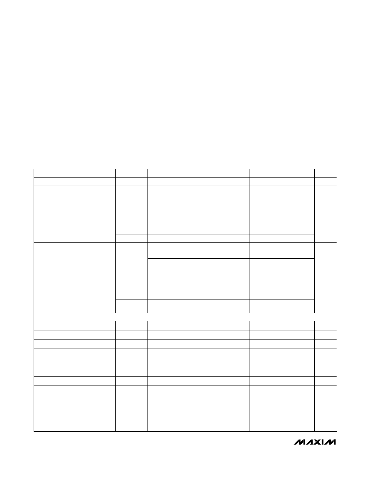
ABSOLUTE MAXIMUM RATINGS
ELECTRICAL CHARACTERISTICS
(DVDD= V
RST
to 3.6V, f
32KIN
= 32.768kHz, TA= -40°C to +85°C, unless otherwise noted.) (Note 1)
Stresses beyond those listed under “Absolute Maximum Ratings” may cause permanent damage to the device. These are stress ratings only, and functional
operation of the device at these or any other conditions beyond those indicated in the operational sections of the specifications is not implied. Exposure to
absolute maximum rating conditions for extended periods may affect device reliability.
Voltage Range on DVDDRelative to DGND ..........-0.5V to +6.0V
Voltage Range on Any Pin Relative to DGND
(3V Tolerant) .........................................-0.5V to (DV
DD
+ 0.5V)
Continuous Output Current
(Any Single I/O Pin)..........................................................25mA
(All I/O Pins Combined) ...................................................25mA
Operating Temperature Range ...........................-40°C to +85°C
Junction Temperature......................................................+150°C
Storage Temperature Range .............................-65°C to +150°C
Soldering Temperature .......................................See IPC/JEDEC
J-STD-020 Specification
Digital Supply Voltage DVDD V
Digital Power-Fail Reset V
Battery Supply Voltage V
Active Current
(Note 2)
Stop-Mode Current
ANALOG VOLTAGE COMPARATOR
Comparator Input-Voltage Range V
Internal Voltage Reference V
Input Offset Voltage VOS (Note 4) -10 +10 mV
Input Common-Mode Voltage V
Common-Mode Rejection Ratio CMMR (Note 4) 55 dB
DC Input-Leakage Current TA = +25°C, CMPx pin in tri-state mode -50 +50 nA
Comparator Setup Time t
Response T ime (CMPx Change
to CMO Valid)
Current Consumed By
Comparator
PARAMETER SYMBOL CONDITIONS MIN TYP MAX UNITS
2.34 2.5 2.71 V
RST
2.0 3.8 V
BAT
I
/1 mode 1.9 2.6
DD1
I
/2 mode 1.3 1.8
DD2
I
/4 mode 1.0 1.4
DD3
I
/8 mode 0.8 1.2
DD4
I
PMM1 mode 0.7 1.0
DD5
Brownout detector disab led
(Note 3), T
I
STOP1
I
STOP2
I
STOP3
INPUT
REF
CMR
CMP_SETUP fSYS
t
CMP_RES P
I
DD_CMP
Brownout detector disab led
(Note 3), T
Brownout detector disab led
(Note 3), T
Brownout detector enabled (Note 3) 16.3 63.0
Brownout detector enabled, RTC enabled
(Note 3)
GND DVDD V
1.15 1.25 1.35 V
(Note 4) 1 DVDD V
= 4.194MHz, V = 20mV (Note 4) 0.8 1.6 μs
f
= 4.194MHz, transition CMPx from
SYS
DGND to DV
(Note 4)
Per enabled comparator, CMONx = 1,
brownout detector enabled, CMPx pins in
tri-state mode
3.3 3.6 V
RST
= +25°C
A
= +60°C
A
= +85°C
A
in ~2ns, t
DD
SYS
= 1/f
SYS
1.9 5.0
2.1 10.0
3.3 35.0
16.4 64.0
140 +
(2 x
t
SYS)
18.0 39.0 μA
600 +
t
(2 x
SYS)
mA
μA
ns
MAXQ3100
Mixed-Signal Microcontroller with Analog
Comparators, LCD, and RTC
_______________________________________________________________________________________ 3
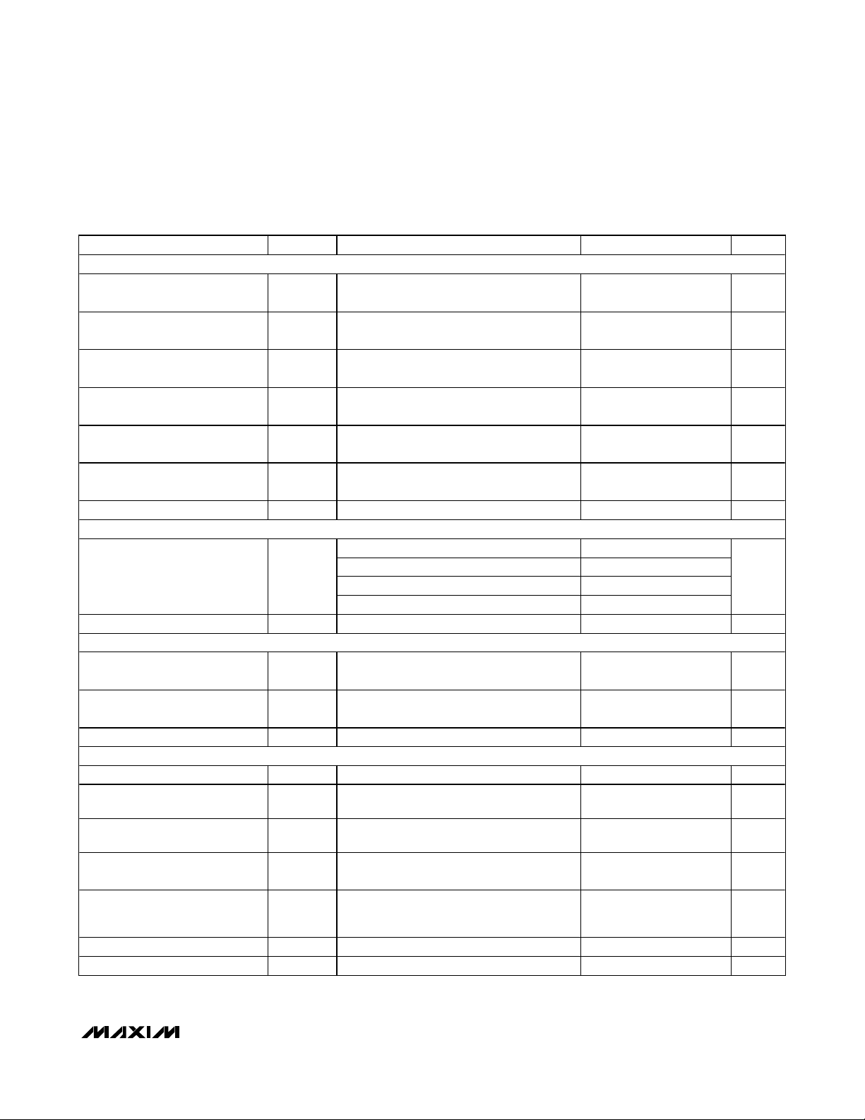
ELECTRICAL CHARACTERISTICS (continued)
(DVDD= V
RST
to 3.6V, f
32KIN
= 32.768kHz, TA= -40°C to +85°C, unless otherwise noted.) (Note 1)
PARAMETER SYMBOL CONDITIONS MIN TYP MAX UNITS
DIGITAL I/O
Input High Voltage (Port 0, 1, 3,
RESET)
Input High Voltage (Port 2) V
V
IH1
IH2
Input Low Voltage VIL
Output High Voltage (Al l Ports) VOH I
Output Low Voltage (Al l Ports,
RESET)
Input Pullup Current I
V
OL
PULLUP
I
DVDD = 3.6V, input mode with weak pullup
enabled
= 3mA
SOURCE
= 4mA 0.4 V
SINK
0.8 x
DV
0.8 x
DV
DV
0.4
DD
DD
DD
5.5 V
DV
DD
+ 0.3
0.2 x
DV
DD
DV
DD
V
V
V
40 120 250 μA
Input Leakage (All Ports) IL Input mode with wea k pullup disabled -50 +50 nA
TEMPERATURE SENSOR
Temperature Conversion Time T
CONV
10-bit resolution, f
11-bit resolution, f
12-bit resolution, f
13-bit resolution, f
= 4.194MH z
SYS
= 4.194MH z
SYS
= 4.194MH z
SYS
= 4.194MH z
SYS
12.5
25
50
100
ms
Temperature Sensor Accuracy ±2 °C
RTC
Battery Supply Current, BatteryBacked Mode
Battery Supply Leakage Current I
I
BAT
BATL
Measured on V
DV
= 0V, RTC enab led
DD
Measured on V
= 3.6V, RTC enabled
DV
DD
BAT
BAT
pin, V
pin, V
BAT
BAT
= 3.6V,
= 3.6V,
1.76 3.1 μA
4 200 nA
Trimm ing Resolut ion One 32.768kHz cloc k per 10s (Note 4) 3.05 ppm
LCD
LCD Supply Voltage V
LCD Bias Voltage 1 V
LCD Bias Voltage 2 V
LCD Adjustment Voltage V
2.4 DVDD V
LCD
V
+ 2/3
(Note 4)
LCD1
(Note 4)
LCD2
(Note 4) 0
ADJ
(V
V
(V
ADJ
LCD
ADJ
LCD
- V
ADJ
+ 1/3
- V
ADJ
)
)
0.4 x
V
LCD
V
V
V
Measured on DVDD pin; LCFG = 0xF7,
LCD Digital Operating Current
I
LCD
LCRA = 0x1B20, LCDx = 0xFF; LCD pins
0.1 μA
are unconnected
LCD Bia s Re sistor R
LCD Adjust Resistor R
40 k
LCD
LRA3:LRA0 = 1111 80 k
LADJ
MAXQ3100
Mixed-Signal Microcontroller with Analog
Comparators, LCD, and RTC
4 _______________________________________________________________________________________
Note 1: Specifications to -40°C are guaranteed by design and are not production tested.
Note 2: Measured on the DV
DD
pin with DVDD= 3.6V, V
BAT
= 3.8V, f
32KIN
= 32.768kHz, executing from EEPROM.
Note 3: Measured on the DV
DD
pin with DVDD= 3.6V, V
BAT
= 3.8V, f
32KIN
= 32.768kHz, all I/O pins disconnected, and not in reset.
Note 4: Specification guaranteed by design but not production tested.
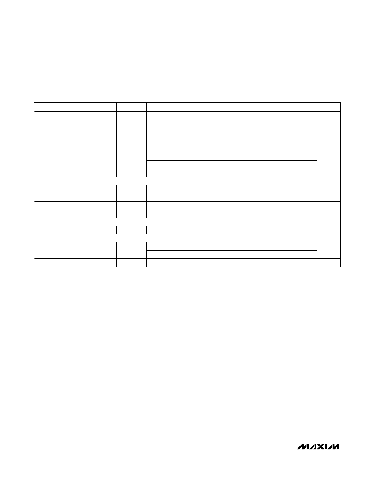
ELECTRICAL CHARACTERISTICS (continued)
(DVDD= V
RST
to 3.6V, f
32KIN
= 32.768kHz, TA= -40°C to +85°C, unless otherwise noted.) (Note 1)
LCD Segment Voltage V
CLOCK SOURCES
External Cry stal Frequency f
Internal Clock Frequency f
System Clock Frequency f
JTAG-COMPATIBLE PROGRAMMING
TCK Frequency f
MEMORY CHARACTERISTICS
EEPROM Write/Era se Cyc les
EEPROM Data Retention Theta-JA = +85°C 50 Years
PARAMETER SYMBOL CONDITIONS MIN TYP MAX UNITS
Segment is driven at V
= -3μA, guaranteed by design
I
SEGxx
Segment is driven at V
= -3μA, guaranteed by design
I
SEGxx
SEGxx
Segment is driven at V
I
= -3μA, guaranteed by design
SEGxx
Segment is driven at V
I
= +3μA, guaranteed by design
SEGxx
32.768 kHz
32KIN
f
CLK
f
SYS
JTAG programming (Note 4) 0 f
TCK
= 32.768kHz, DVDD = 3.6V 4.110 4.194 4.278 MH z
32KIN
= f
SYS
/ system clock divisor
CLK
LCD
LCD1
LCD2
ADJ
; V
; V
; V
; V
LCD
LCD1
LCD2
ADJ
= 3V,
= 2V,
= 1V,
= 0V,
Theta- JA = +25°C 200,000
Theta- JA = +85°C 50,000
V
-
LCD
0.06
V
LCD1
0.04
V
LCD2
0.02
V
f
CLK /
256
ADJ
V
V
V
0.1
f
LCD
LCD1
LCD2
CLK
/ 8 MHz
SYS
V
Cycles
MAXQ3100
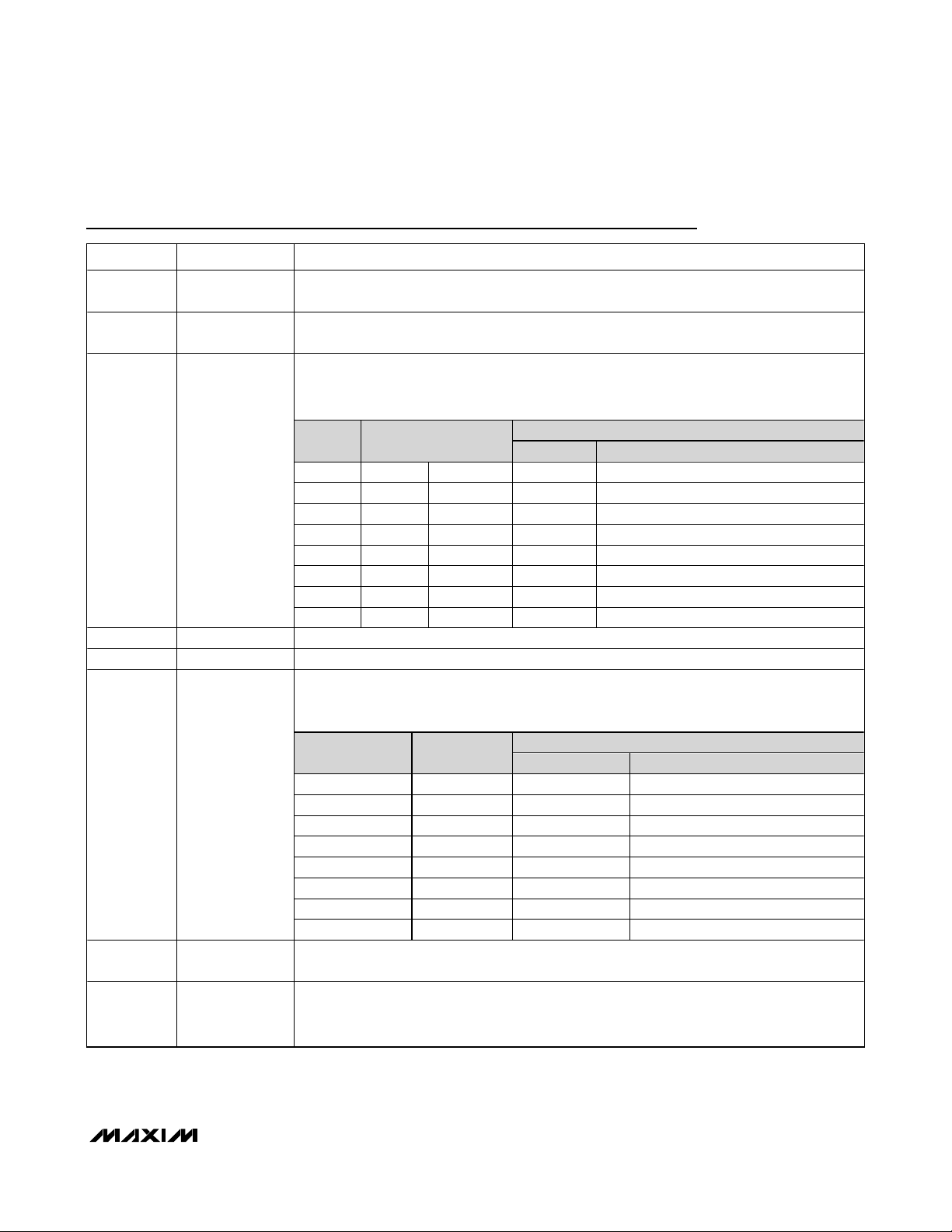
Pin Description
PIN NAME FUNCTION
1, 11, 52,
58, 75
DGND
Digital Ground
6, 53, 59,
76
DV
DD
Digital Supply Voltage (+3.3V)
General-Purpose, Digital, I/O, Type D Port; External Edge-Selectable Interrupt. These port
pins function as bidirectional I/O pins only. All port pins default to input mode with weak
pullups enabled after a reset. All port pins can be configured as external interrupt inputs. All
alternate function s must be enabled from software.
SPECIAL/ALTERNATE FUNCTION
PIN NAME
NAME FUNCTION
77 P0.0 INT0 TXD0 Serial Port 0 Tran sm it
78 P0.1 INT1 RXD0 Serial Port 0 Receive
79 P0.2 INT2 T0G Timer 0 Gate Input
80 P0.3 INT3 T0 Timer 0 Input
2 P0.4 INT4 T1 Timer 1 Input/Output
3 P0.5 INT5 T1EX Timer 1 External Capture/Reload Input
4 P0.6 INT6 — —
2–5, 77–80
P0.0–P0.7;
INT0–INT7;
TXD0, RXD0,
T0G, T0, T1, EX
5 P0.7 INT7 — —
7–10 COM0–COM3
Dedicated LCD Common-Voltage Outputs
12–43 SEG1–SEG31
Dedicated LCD Drive Outputs
General-Purpose, Digital, I/O, Type C Port; LCD Segment-Driver Output. These port pins
function as bidirectional I/O pins and LCD segment-driver outputs. All alternate functions
must be enabled from software.
SPECIAL/ALTERNATE FUNCTION
PIN NAME
NAME FUNCTION
44 P2.0 SEG32 LCD Segment 32
45 P2.1 SEG33 LCD Segment 33
46 P2.2 SEG34 LCD Segment 34
47 P2.3 SEG35 LCD Segment 35
48 P2.4 SEG36 LCD Segment 36
49 P2.5 SEG37 LCD Segment 37
50 P2.6 SEG38 LCD Segment 38
44–51
P2.0–P2.7;
SEG32–SEG39
51 P2.7 SEG39 LCD Segment 39
54
V
LCD
LCD Bias-Control Voltage. Highest LCD drive voltage used in all bias modes. This pin
must be connected to an external supply when using the LCD display controller.
55
V
LCD1
LCD Bias, Voltage 1. Next highest LCD drive voltage, used in 1/2 and 1/3 LCD bias modes.
An internal resistor-divider sets the voltage at this pin. External resistor s and capacitors
can be used to change LCD voltage or drive capability at this pin. This pin must be shunted
externally to V
LCD2
when using 1/2 bias mode.
Mixed-Signal Microcontroller with Analog
Comparators, LCD, and RTC
_______________________________________________________________________________________ 5
MAXQ3100
Mixed-Signal Microcontroller with Analog
Comparators, LCD, and RTC
6 _______________________________________________________________________________________
Pin Description (continued)
PIN NAME FUNCTION
56
V
LCD2
LCD Bias, Voltage 2. Third highest LCD drive voltage, used in 1/3 LCD bias mode only. An
internal resistor-divider sets the voltage at this pin. External resistor s and capacitors can be
used to change LCD voltage or drive capability at this pin. This pin must be shunted
externally to V
LCD1
when using 1/2 bias mode.
57
V
ADJ
LCD Adjustment Voltag e. Lowest LCD drive voltage, u sed in al l bias modes . Connect to
DGND through an external resistor to provide external control of the LCD contrast. Leave
disconnected for internal contrast adjustment.
General-Purpose, Digital, I/O, Type D Port; External Edge-Selectable Interrupt. These port
pins function as bidirectional I/O pins only. All port pins default to input mode with weak
pullups enabled after a reset. Port pins P1.0–P1.3 can be configured as external interrupt
inputs. Al l alternate funct ions must be enabled from software.
SPECIAL/ALTERNATE FUNCTION
PIN NAME
NAME FUNCTION
60 P1.0 INT8 T2B Timer 2 Secondary I/O
61 P1.1 INT9 T2A Timer 2 Primary I/O
62 P1.2 INT10 TXD1 Serial Port 1 Transmit
60–63
P1.0–P1.3;
INT8–INT11;
T2B, T2A, TXD1,
RXD1
63 P1.3 INT11 RXD1 Serial Port 1 Receive
General-Purpose, Digital, I/O, Type C Port; External Edge-Selectable Interrupt. These port
pins function as bidirectional I/O pins only. All port pins default to input mode with weak
pullups enabled after a reset. All alternate functions must be enab led from software, except
for the JTAG-compatible functions that are enabled by default fo llowing reset.
SPECIAL/ALTERNATE FUNCTION
PIN NAME
NAME FUNCTION
64 P3.0 TDI JT AG TAP Data Input
65 P3.1 TDO JTAG TAP Data Output
66 P3.2 TCK JT AG TAP Clock Input
67 P3.3 TMS JTAG TAP Mode-Select Input
68 P3.4 SQW RTC Square-Wave Output
69 P3.5 CMP0 Analog Comparator Input 0
64–70
P3.0–P3.6;
TDI, TDO, TCK,
TMS, SWQ,
CMP0, CMP1
70 P3.6 CMP1 Analog Comarator Input 1
71
RESET
Active-Low, Digital Reset Input/Output. The CPU i s held in reset when thi s pin is low and
begins executing from the reset vector when released. The pin must be pulled high by an
external 50k resistor. This pin is driven low as an output when an internal reset condition
occurs.
72
V
BAT
Digital Battery-Backup Supply. This supply provides an optional battery backup for the
RTC when DV
DD
power is removed. If this pin is connected to a nominal 3.3V battery then
the RTC will operate and battery-backed register contents will be preserved when DV
DD
is
removed. If battery backup is not required this pin should be connected directly to DV
DD
.
73 32KIN
74 32KOUT
32kHz Crystal Input/Output. Connect an external, 6pF 32kHz watch crystal between 32KIN
and 32KOUT to generate the system clock.
MAXQ3100
Mixed-Signal Microcontroller with Analog
Comparators, LCD, and RTC
_______________________________________________________________________________________ 7
Detailed Description
The following is an introduction to the primary features
of the microcontroller. More detailed descriptions of the
device features can be found in the data sheets, errata
sheets, and user’s guides described later in the
Additional Documentation
section.
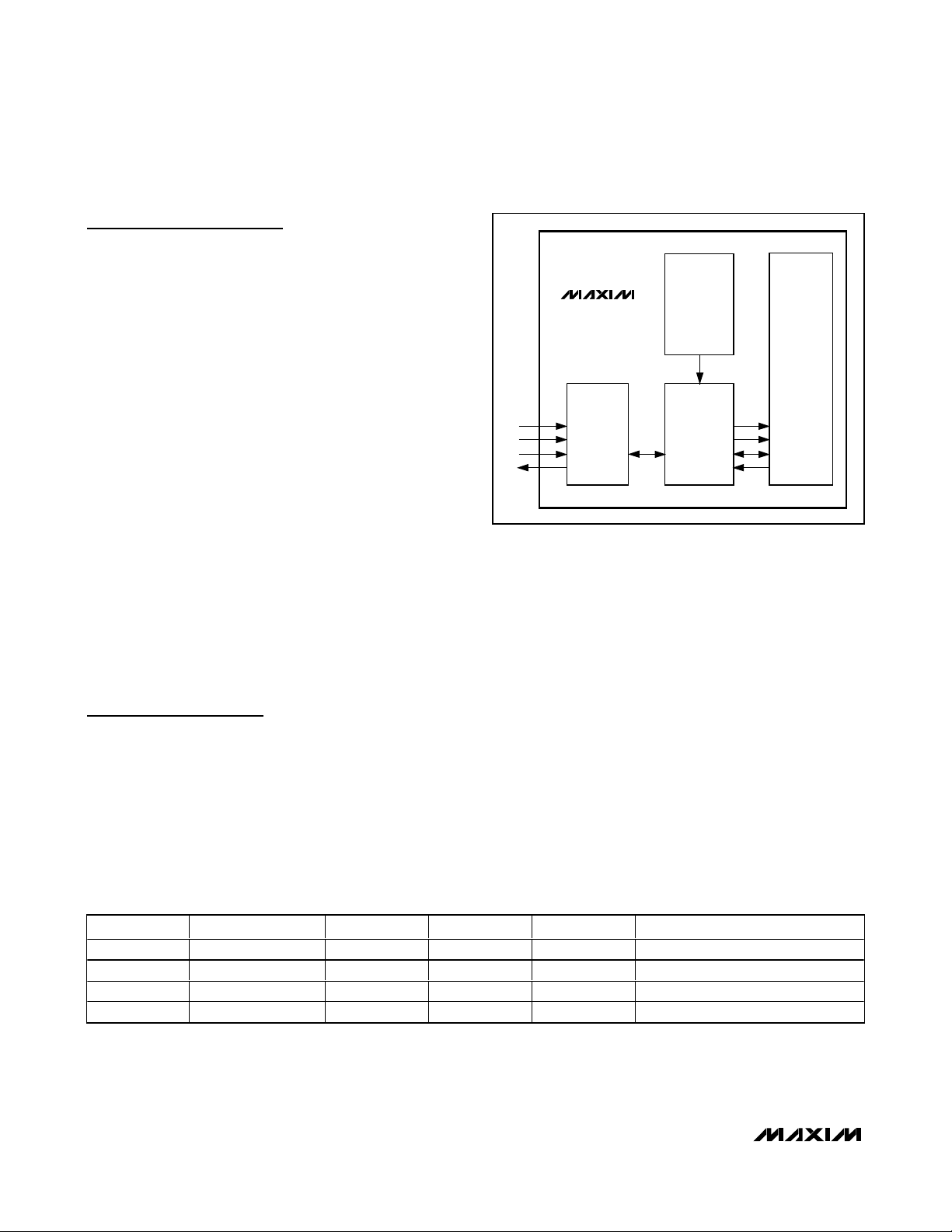
MAXQ Core Architecture
The MAXQ3100 is a high-performance, CMOS, 16-bit
RISC microcontroller with EEPROM and an integrated
160-segment LCD controller. It is structured on a highly
advanced, accumulator-based, 16-bit RISC architecture. Fetch and execution operations are completed in
one cycle without pipelining, because the instruction
contains both the op code and data. The result is a
streamlined 4.194 million instructions-per-second
(MIPS) microcontroller.
The highly efficient core is supported by a 16-level
hardware stack, enabling fast subroutine calling and
task switching. Data can be quickly and efficiently
manipulated with three internal data pointers. Multiple
data pointers allow more than one function to access
data memory without having to save and restore data
pointers each time. The data pointers can automatically
increment or decrement following an operation, eliminating the need for software intervention. As a result,
the application speed is greatly increased.
Functional Diagram
ANALOG COMPARATOR
8kW EEPROM
(PROGRAM)
TIMER 0-TYPE
16-BIT TIMER/COUNTER
TIMER 1-TYPE
16-BIT TIMER/COUNTER
TIMER 2-TYPE
16-BIT TIMER/COUNTER
SERIAL USART
SERIAL USART WITH
INFRARED PWM
SUPPORT
DIGITAL TEMPERATURE
SENSOR
512W SRAM
(D ATA)
(16 x 16-BIT ACCUMULATORS)
WATCHDOG TIMER
POWER REDUCTION/
CLOCK GENERATION
POR
JTAG
TMS
TDI
TDO
TCK
2kW UTILITY ROM
+1.25V
REFERENCE
ANALOG COMPARATOR
3.3V
160-SEGMENT LCD
DRIVER
REAL-TIME CLOCK
EXTERNAL 32.768kHz
CRYSTAL
MAXQ20 RISC CORE
MAXQ3100

MAXQ3100
Mixed-Signal Microcontroller with Analog
Comparators, LCD, and RTC
8 _______________________________________________________________________________________
Instruction Set
The instruction set is composed of fixed-length, 16-bit
instructions that operate on registers and memory locations. The instruction set is highly orthogonal, allowing
arithmetic and logical operations to use any register
along with the accumulator. Special-function registers
control the peripherals and are subdivided into register
modules. The family architecture is modular, so that
new devices and modules can reuse code developed
for existing products.
The architecture is transport-triggered. This means that
writes or reads from certain register locations can also
cause side effects to occur. These side effects form the
basis for the higher-level op codes defined by the
assembler, such as ADDC, OR, JUMP, etc. The op
codes are actually implemented as MOVE instructions
between certain system register locations, while the
assembler handles the encoding, which need not be a
concern to the programmer.
The 16-bit instruction word is designed for efficient execution. Bit 15 indicates the format for the source field of
the instruction. Bits 0 to 7 of the instruction represent the
source for the transfer. Depending on the value of the
format field, this can either be an immediate value or a
source register. If this field represents a register, the
lower four bits contain the module specifier and the
upper four bits contain the register index in that module.
Bits 8 to 14 represent the destination for the transfer. This
value always represents a destination register, with the
lower four bits containing the module specifier and the
upper three bits containing the register subindex within
that module.
Anytime that it is necessary to directly select one of the
upper 24 index locations in a destination module, the
prefix register PFX is needed to supply the extra destination bits. This prefix register write is inserted automatically by the assembler and requires only one
additional execution cycle.
Memory Organization
The device incorporates several memory areas:
• 2kWords utility ROM
• 8kWords of EEPROM for program storage
• 512 words of SRAM for storage of temporary
variables
• 16-level, 16-bit-wide stack memory for storage of
program return addresses and general-purpose use
The memory is arranged by default in a Harvard architecture, with separate address spaces for program and
data memory. The configuration of program and data
space depends on the current execution location.
• When executing code from EEPROM memory, the
SRAM and utility ROM are accessible in data space.
• When executing code from SRAM, the EEPROM and
utility ROM are accessible in data space.
• When executing code from the utility ROM, the
EEPROM memory and SRAM are accessible in data
space.
Refer to the
MAXQ Family User’s Guide: MAXQ3100
Supplement
for more details.
In all cases, whichever memory segment is currently
being executed from cannot be accessed in data space.
To allow the use of lookup tables and similar constructs
in the memory, the utility ROM contains a set of lookup
and block copy routines (refer to the user’s guide supplement for more details).
The incorporation of EEPROM allows the device to be
reprogrammed, eliminating the expense of throwing
away one-time programmable devices during development and field upgrades. Program memory can be
password protected with a 16-word key, denying
access to program memory by unauthorized individuals.
Stack Memory
A 16-bit-wide internal stack provides storage for program return addresses and general-purpose use. The
stack is used automatically by the processor when the
CALL, RET, and RETI instructions are executed and
interrupts serviced. The stack can also be used explicitly to store and retrieve data by using the PUSH, POP,
and POPI instructions.
On reset, the stack pointer, SP, initializes to the top of
the stack (0Fh). The CALL, PUSH, and interrupt-vectoring operations increment SP, then store a value at the
stack location pointed to by SP. The RET, RETI, POP,
and POPI operations retrieve the value at the stack
location pointed to by SP, and then decrement SP.
Utility ROM
The utility ROM is a 2kWord block of internal ROM
memory that defaults to a starting address of 8000h.
The utility ROM consists of subroutines that can be
called from application software. These include:
• In-system programming (bootloader) over the JTAGcompatible debug port
• In-circuit debug routines
• User-callable routines for in-application flash programming and code space table lookup
MAXQ3100
Mixed-Signal Microcontroller with Analog
Comparators, LCD, and RTC
_______________________________________________________________________________________ 9
Figure 1. Memory Map When Executing from EEPROM
PROGRAM
SPACE
DATA SPACE
(BYTE MODE)
DATA SPACE
(WORD MODE)
EXECUTING FROM
512 x 16
DATA SRAM
2k x 16
UTILITY ROM
8k x 16
PROGRAM EEPROM
A1FFh
A000h
87FFh
8000h
1FFFh
0000h
4k x 8
UTILITY ROM
1k x 8
DATA SRAM
8FFFh
8000h
03FFh
0000h
2k x 16
UTILITY ROM
512 x 16
DATA SRAM
87FFh
8000h
01FFh
0000h

MAXQ3100
Mixed-Signal Microcontroller with Analog
Comparators, LCD, and RTC
10 ______________________________________________________________________________________
Following any reset, execution begins in the utility
ROM. The ROM software determines whether the program execution should immediately jump to the start of
user-application code (located at address 0000h), or to
the bootloader. Routines within the utility ROM are useraccessible and can be called as subroutines by the
application software. More information on the utility
ROM contents is contained in the user’s guide supplement for this device.
Some applications require protection against unauthorized viewing of program code memory. For these
applications, access to in-system programming, inapplication programming, or in-circuit debugging functions is prohibited until a password has been supplied.
A single password-lock (PWL) bit is implemented in the
SC register. When the PWL is set to one (power-on
reset default), the password is required to access the
utility ROM, including in-circuit debug and in-system
programming routines that allow reading or writing of
internal memory. When PWL is cleared to zero, these
utilities are fully accessible without the password. The
password is automatically set to all ones following a
mass erase.
Programming
The microcontroller’s EEPROM can be programmed by
two different methods: in-system programming and inapplication programming. Both methods afford great flexibility in system design as well as reduce the life-cycle
cost of the embedded system. In-system programming
can be password protected to prevent unauthorized
access to code memory.
In-System Programming
An internal bootloader allows the device to be reloaded
over a simple JTAG-compatible debug port. As a result,
system software can be upgraded in-system, eliminating
the need for a costly hardware retrofit when software
updates are required. Remote software uploads are possible that enable physically inaccessible applications to
be frequently updated. The interface hardware can be a
JTAG connection to another microcontroller, or a connection to a PC serial port using a serial-to-JTAG converter such as the one included in the MAXQ3100
evaluation kit. If in-system programmability is not
required, a commercial gang programmer can be used
for mass programming.
Activating the debug port and loading the test access
port (TAP) with the system programming instruction
invokes the bootloader. Setting the SPE bit to 1 during
reset through the debug port executes the bootloadermode program that resides in the utility ROM. When programming is complete, the bootloader can clear the
SPE bit and reset the device, allowing the device to
bypass the utility ROM and begin execution of the application software.
The following bootloader functions are supported:
•Load
• Dump
• CRC
• Verify
• Erase
In-Application Programming
The in-application programming feature allows the
microcontroller to modify its own program memory from
its application software. This allows on-the-fly software
updates in mission-critical applications that cannot
afford downtime. Alternatively, it allows the application
to develop custom loader software that can operate
under the control of the application software. The utility
ROM contains user-accessible programming functions
that erase and program memory. These functions are
described in detail in the user’s guide supplement for
this device.
Register Set
Most functions of the device are controlled by sets of
registers. These registers provide a working space for
memory operations as well as configuring and addressing peripheral registers on the device. Registers are
divided into two major types: system registers and
peripheral registers. The common register set, also
known as the system registers, includes the ALU, accumulator registers, data pointers, interrupt vectors and
control, and stack pointer. The peripheral registers
define additional functionality that may be included by
different products based on the MAXQ architecture.
This functionality is broken up into discrete modules so
that only the features required for a given product need
to be included. Tables 1 and 4 show the MAXQ3100
register set.

MAXQ3100
Mixed-Signal Microcontroller with Analog
Comparators, LCD, and RTC
______________________________________________________________________________________ 11
Table 1. System Register Map
Note: Names that appear in italics indicate that all bits of a register are read-only. Names that appear in bold indicate that a register
is 16 bits wide. Registers in module AP are bit addressable.
REGISTER
INDEX
0h AP A[0] PFX IP — — —
1h APC A[1] — — SP — —
2h — A[2] — — IV — —
3h — A[3] — — — Offs DP[0]
4h PSF A[4] — — — DPC —
5h IC A[5] — — — GR —
6h IMR A[6] — — LC[0] GRL —
7h — A[7] — — LC[1] BP DP[1]
8h SC A[8] — — — GRS —
9h — A[9] — — — GRH —
Ah — A[10] — — — GRXL —
Bh IIR A[11] — — — BP[offs] —
Ch — A[12] — — — — —
Dh — A[13] — — — — —
Eh CKCN A[14] — — — — —
Fh WDCN A[15] — — — — —
AP
(8h)
A
(9h)
MODULE NAME (BASE SPECIFIER)
PFX
(Bh)
IP
(Ch)
SP
(Dh)
DPC
(Eh)
DP
(Fh)

MAXQ3100
Mixed-Signal Microcontroller with Analog
Comparators, LCD, and RTC
12 ______________________________________________________________________________________
Table 2. System Register Bit Functions
REGISTER
AP — — — — AP (4 bits)
APC CLR IDS — — — MOD2 MOD1 MOD0
PSF Z S — GPF1 GPF0 OV C E
IC — — CGDS — — — INS IGE
IMR IMS — — — IM3 — IM1 IM0
SC TAP — — — — — PWL —
IIR IIS — — — II3 — II1 II0
CKCN — — — STOP SWB PMME CD1 CD0
WDCN POR EWDI WD1 WD0 WDIF WTRF EWT RWT
A[0..15] A[n] (16 bits)
PFX PFX (16 bits)
IP IP (16 bits)
SP — — — — — — — — — — — — SP (4 bits)
IV IV (16 bits)
LC[0] LC[0] (16 bits)
LC[1] LC[1] (16 bits)
Offs Offs (8 bits)
DPC — — — — — — — — — — — WBS2 WBS1 WBS0 SDPS1 SDPS0
GR GR (16 bits)
GRL GR.7 GR.6 GR.5 GR.4 GR.3 GR.2 GR.1 GR.0
BP BP (16 bits)
GRS GR.7 GR.6 GR.5 GR.4 GR.3 GR.2 GR.1 GR.0 GR.15 GR.14 GR.13 GR.12 GR.11 GR.10 GR.9 GR.8
GRH GR.15 GR.14 GR.13 GR.12 GR.11 GR.10 GR.9 GR.8
GRXL GR.7 GR.7 GR.7 GR.7 GR.7 GR.7 GR.7 GR.7 GR.7 GR.6 GR.5 GR.4 GR.3 GR.2 GR.1 GR.0
BP[offs] BP[offs] (16 bits)
DP[0] DP[0] (16 bits)
DP[1] DP[1] (16 bits)
1514131211109876543210
REGISTER BIT
MAXQ3100
Mixed-Signal Microcontroller with Analog
Comparators, LCD, and RTC
______________________________________________________________________________________ 13
Table 3. System Register Reset Values
Note: Bits marked with an “s” have special behavior upon reset. Refer to the user’s guide supplement for this device for more
details.
REGISTER
AP 00000000
APC 00000000
PSF 10000000
IC 00000000
IMR 00000000
SC 100000s 0
IIR 00000000
CKCN 10000000
WDCN ss000ss0
A[0..15] 0000000000000000
PFX 0000000000000000
IP 1000000000000000
SP 0000000000001111
IV 0000000000000000
LC[0] 0000000000000000
LC[1] 0000000000000000
Offs 00000000
DPC 0000000000011100
GR 0000000000000000
GRL 00000000
BP 0000000000000000
GRS 0000000000000000
GRH 00000000
GRXL 0000000000000000
BP[offs] 0000000000000000
DP[0] 0000000000000000
DP[1] 0000000000000000
1514131211109876543210
REGISTER BIT

MAXQ3100
Mixed-Signal Microcontroller with Analog
Comparators, LCD, and RTC
14 ______________________________________________________________________________________
Table 4. Peripheral Register Map
Note: Names that appear in italics indicate that all bits of a register are read-only. Names that appear in bold indicate that a register
is 16 bits wide.
REGISTER INDEX
0h PO0 PO1 PO2 PO3
1h SCON0 SCON1 LCFG RTRM
2h SBUF0 SBUF1 LCRA RCNT
3h T0CN T2CNB LCD0 CCN0
4h T0L T2H LCD1 CCN1
5h T1CN T2RH LCD2 —
6h T1MD T2CH LCD3 TEMPR
7h EIF0 EIF1 LCD4 TPCFG
8h PI0 PI1 PI2 PI3
9h SMD0 SMD1 LCD5 RTSS
Ah PR0 PR1 LCD6 RTSH
Bh T0H T2CNA LCD7 RTSL
Ch T1L T2CFG LCD8 RSSA
Dh T1H T2V LCD9 RASH
Eh T1CL T2C LCD10 RASL
Fh T1CH IRCN LCD11 PWCN
10h PD0 PD1 PD2 PD3
11h
12h
13h
14h
15h
16h
17h
18h
19h
1Ah
1Bh
1Ch
1Dh
1Eh EIE0 EIE1 — —
1Fh EIES0 EIES1 — —
M0
(0h)
—
—
—
—
—
—
—
—
—
—
—
—
—
M1
(1h)
T2R LCD12 —
— LCD13 —
— LCD14 —
— LCD15 —
— LCD16 —
— LCD17 —
— LCD18 —
— LCD19 —
———
———
———
———
———
M2
(2h)
M3
(3h)

MAXQ3100
Mixed-Signal Microcontroller with Analog
Comparators, LCD, and RTC
______________________________________________________________________________________ 15
Table 5. Peripheral Register Bit Functions
REGISTER BIT
15 14 13 12 11 10 9 8 7 6 5 4 3 2 1 0
T0H.6 T0H.5 T0H.4 T0H.3 T0H.2 T0H.1 T0H.0
PR1.6 PR1.5 PR1.4 PR1.3 PR1.2 PR1.1 PR1.0
PO0 PO0.7 PO0.6 PO0.5 PO0.4 PO0.3 PO0.2 PO0.1 PO0.0
REGISTER
SCON0 SM0/FE SM1 SM2 REN TB8 RB8 TI RI
T0CN ET0 T0M TF0 TR0 GATE C/T M1 M0
SBUF0 SBUF0.7 SBUF0.6 SBUF0.5 SBUF0.4 SBUF0.3 SBUF0.2 SBUF0.1 SBUF0.0
T0L T0L.7 T0L.6 T0L.5 T0L.4 T0L.3 T0L.2 T0L.1 T0L.0
T1CN TF1 EXF1 T1OE DCEN EXEN1 TR1 C/T1 CP/RL1
T1MD — ——— — —ET1T1M
EIF0 IE7 IE6 IE5 IE4 IE3 IE2 IE1 IE0
PI0 PI0.7 PI0.6 PI0.5 PI0.4 PI0.3 PI0.2 PI0.1 PI0.0
SMD0 EIR OFS — — — ESI SMOD FEDE
PR0 PR0.15 PR0.14 PR0.13 PR0.12 PR0.11 PR0.10 PR0.9 PR0.8 PR0.7 PR0.6 PR0.5 PR0.4 PR0.3 PR0.2 PR0.1 PR0.0
T0H T0H.7
T1L T1L.7 T1L.6 T1L.5 T1L.4 T1L.3 T1L.2 T1L.1 T1L.0
T1H T1H.7 T1H.6 T1H.5 T1H.4 T1H.3 T1H.2 T1H.1 T1H.0
PD0 PD0.7 PD0.6 PD0.5 PD0.4 PD0.3 PD0.2 PD0.1 PD0.0
T1CL T1CL.7 T1CL.6 T1CL.5 T1CL.4 T1CL.3 T1CL.2 T1CL.1 T1CL.0
EIE0 EX7 EX6 EX5 EX4 EX3 EX2 EX1 EX0
EIES0 IT7 IT6 IT5 IT4 IT3 IT2 IT1 IT0
PO1 — — — — PO1.3 PO1.2 PO1.1 PO1.0
SCON1 SM0/FE SM1 SM2 REN TB8 RB8 TI RI
SBUF1 SBUF1.7 SBUF1.6 SBUF1.5 SBUF1.4 SBUF1.3 SBUF1.2 SBUF1.1 SBUF1.0
T2CNB ET2L T2OE1 T2POL1 — TF2 TF2L TCC2 TC2L
T2H T2V.15 T2V.14 T2V.13 T2V.12 T2V.11 T2V.10 T2V.9 T2V.8
T2RH T2R.15 T2R.14 T2R.13 T2R.12 T2R.11 T2R.10 T2R.9 T2R.8
T2CH T2C.15 T2C.14 T2C.13 T2C.12 T2C.11 T2C.10 T2C.9 T2C.8
EIF1 — — — — IE11 IE10 IE9 IE8
PI1 — — — — PI1.3 PI1.2 PI1.1 PI1.0
SMD1 — — — — — ESI SMOD FEDE
PR1 PR1.15 PR1.14 PR1.13 PR1.12 PR1.11 PR1.10 PR1.9 PR1.8 PR1.7

MAXQ3100
Mixed-Signal Microcontroller with Analog
Comparators, LCD, and RTC
16 ______________________________________________________________________________________
Table 5. Peripheral Register Bit Functions (continued)
PO2.6 PO2.5 PO2.4 PO2.3 PO2.2 PO2.1 PO2.0
REGISTER BIT
T2V.14 T2V.13 T2V.12 T2V.11 T2V.10 T2V.9 T2V.8 T2V.7 T2V.6 T2V.5 T2V.4 T2V.3 T2V.2 T2V.1 T2V.0
T2C.14 T2C.13 T2C.12 T2C.11 T2C.10 T2C.9 T2C.8 T2C.7 T2C.6 TCV.5 TCV.4 TCV.3 TCV.2 TCV.1 TCV.0
15 14 13 12 11 10 9 8 7 6 5 4 3 2 1 0
T2V T2V.15
T2CNA ET2 T2OE0 T2POL0 TR2L TR2 CPRL2 SS2 G2EN
REGISTER
T2CFG T2CI DIV2 DIV1 DIV0 T2MD CCF1 CCF0 C/T2
T2C T2C.15
IRCN — — — — — IREN IRTX IRBB
PD1 — — — — PD1.3 PD1.2 PD1.1 PD1.0
T2R T2R.15 T2R.14 T2R.13 T2R.12 T2R.11 T2R.10 T2R.9 T2R.8 T2R.7 T2R.6 T2R.5 T2R.4 T2R.3 T2R.2 T2R.1 T2R.0
EIE1 — — — — EX11 EX10 EX9 EX8
EIES1 — — — — IT11 IT10 IT9 IT8
PO2 PO2.7
LCFG PCF3 PCF2 PCF1 PCF0 — SMO OPM DPE
LCRA — — — DUTY1 DUTY0 FRM3 FRM2 FRM1 FRM0 — LRIG — LRA3 LRA2 LRA1 LRA0
LCD0 LCD0.7 LCD0.6 LCD0.5 LCD0.4 LCD0.3 LCD0.2 LCD0.1 LCD0.0
LCD1 LCD1.7 LCD1.6 LCD1.5 LCD1.4 LCD1.3 LCD1.2 LCD1.1 LCD1.0
LCD2 LCD2.7 LCD2.6 LCD2.5 LCD2.4 LCD2.3 LCD2.2 LCD2.1 LCD2.0
LCD3 LCD3.7 LCD3.6 LCD3.5 LCD3.4 LCD3.3 LCD3.2 LCD3.1 LCD3.0
LCD4 LCD4.7 LCD4.6 LCD4.5 LCD4.4 LCD4.3 LCD4.2 LCD4.1 LCD4.0
PI2 PI2.7 PI2.6 PI2.5 PI2.4 PI2.3 PI2.2 PI2.1 PI2.0
LCD5 LCD5.7 LCD5.6 LCD5.5 LCD5.4 LCD5.3 LCD5.2 LCD5.1 LCD5.0
LCD6 LCD6.7 LCD6.6 LCD6.5 LCD6.4 LCD6.3 LCD6.2 LCD6.1 LCD6.0
LCD7 LCD7.7 LCD7.6 LCD7.5 LCD7.4 LCD7.3 LCD7.2 LCD7.1 LCD7.0
LCD8 LCD8.7 LCD8.6 LCD8.5 LCD8.4 LCD8.3 LCD8.2 LCD8.1 LCD8.0
LCD9 LCD9.7 LCD9.6 LCD9.5 LCD9.4 LCD9.3 LCD9.2 LCD9.1 LCD9.0
LCD10 LCD10.7 LCD10.6 LCD10.5 LCD10.4 LCD10.3 LCD10.2 LCD10.1 LCD10.0
PD2 PD2.7 PD2.6 PD2.5 PD2.4 PD2.3 PD2.2 PD2.1 PD2.0
LCD11 LCD11.7 LCD11.6 LCD11.5 LCD11.4 LCD11.3 LCD11.2 LCD11.1 LCD11.0
LCD12 LCD12.7 LCD12.6 LCD12.5 LCD12.4 LCD12.3 LCD12.2 LCD12.1 LCD12.0

MAXQ3100
Mixed-Signal Microcontroller with Analog
Comparators, LCD, and RTC
______________________________________________________________________________________ 17
Table 5. Peripheral Register Bit Functions (continued)
— — BOD
CCN1 CMON CMIE CMF CMM — CMO CMPOL —
TEMPR.7 TEMPR.5 TEMPR.5 TEMPR.4 TEMPR.3 TEMPR.2 TEMPR.1 TEMPR.0
.8
TEMPR
.9
TEMPR
.10
TEMPR
.11
TEMPR
.12
TEMPR
.13
TEMPR
.14
TEMPR
.15
TEMPR
TEMPR
TPCFG TPIF TPIE — — — RES1 RES0 START
REGISTER BIT
15 14 13 12 11 10 9 8 7 6 5 4 3 2 1 0
LCD13 LCD13.7 LCD13.6 LCD13.5 LCD13.4 LCD13.3 LCD13.2 LCD13.1 LCD13.0
REGISTER
LCD14 LCD14.7 LCD14.6 LCD14.5 LCD14.4 LCD14.3 LCD14.2 LCD14.1 LCD14.0
LCD15 LCD15.7 LCD15.6 LCD15.5 LCD15.4 LCD15.3 LCD15.2 LCD15.1 LCD15.0
LCD16 LCD16.7 LCD16.6 LCD16.5 LCD16.4 LCD16.3 LCD16.2 LCD16.1 LCD16.0
LCD17 LCD17.7 LCD17.6 LCD17.5 LCD17.4 LCD17.3 LCD17.2 LCD17.1 LCD17.0
LCD18 LCD18.7 LCD18.6 LCD18.5 LCD18.4 LCD18.3 LCD18.2 LCD18.1 LCD18.0
PO3 — PO3.6 PO3.5 PO3.4 PO3.3 PO3.2 PO3.1 PO3.0
LCD19 LCD19.7 LCD19.6 LCD19.5 LCD19.4 LCD19.3 LCD19.2 LCD19.1 LCD19.0
RTRM TSGN TRM6 TRM5 TRM4 TRM3 TRM2 TRM1 TRM0
RCNT WE — — — — — FT SQE ALSF ALDF RDYE RDY BUSY ASE ADE RTCE
CCN0 CMON CMIE CMF CMM — CMO CMPOL —
PI3 — PI3.6 PI3.5 PI3.4 PI3.3 PI3.2 PI3.1 PI3.0
RTSH.
RTSH.
RTSH.
RTSH.
RTSH.
RTSH.
RTSH.
RTSH.
RTSS RTSS.7 RTSS.6 RTSS.5 RTSS.4 RTSS.3 RTSS.2 RTSS.1 RTSS.0
RTSH.7 RTSH.6 RTSH.5 RTSH.4 RTSH.3 RTSH.2 RTSH.1 RTSH.0
8
RTSL.
9
RTSL.
10
RTSL.
11
RTSL.
12
RTSL.
13
RTSL.
14
RSTL.
15
RTSL.
RTSH
RSTL.7 RTSL.6 RTSL.5 RTSL.4 RTSL.3 RTSL.2 RTSL.1 RTSL.0
8
RSSA.
9
RSSA.
10
RSSA.
11
RSSA.
12
RSSA.
13
RSSA.
14
RSSA.
15
RSSA.
RTSL
RSSA.7 RSSA.6 RSSA.5 RSSA.4 RSSA.3 RSSA.2 RSSA.1 RSSA.0
8
9
10
11
12
13
14
15
RSSA
RASL.7 RASL.6 RASL.5 RASL.4 RASL.3 RASL.2 RASL.1 RASL.0
RASL.
RASL.
RASL.
RASL.
RASL.
RASL.
RASL.
RASL.
RASL
RASH — — — — RASH.3 RASH.2 RASH.1 RASH.0
8
9
10
11
12
13
14
15
———— —
PD3 — PD3.6 PD3.5 PD3.4 PD3.3 PD3.2 PD3.1 PD3.0
PWCN

MAXQ3100
Mixed-Signal Microcontroller with Analog
Comparators, LCD, and RTC
18 ______________________________________________________________________________________
Note: Bits marked with an “s” have special behavior upon reset. Refer to the user’s guide supplement for this device for more details.
Table 6. Peripheral Register Bit Reset Values
REGISTER
PO0 11111111
SCON0 00000000
SBUF0 00000000
T0CN 00000000
T0L 00000000
T1CN 00000000
T1MD 00000000
EIF0 00000000
PI0 ssssssss
SMD0 00000000
PR0 0000000000000000
T0H 00000000
T1L 00000000
T1H 00000000
T1CL 00000000
T1CH 00000000
PD0 00000000
EIE0 00000000
EIES0 00000000
PO1 00001111
SCON1 00000000
SBUF1 00000000
T2CNB 00000000
T2H 00000000
T2RH 00000000
T2CH 00000000
EIF1 00000000
PI1 0000ssss
SMD1 00000000
PR1 0000000000000000
T2CNA 00000000
T2CFG 00000000
T2V 0
T2C 0
IRCN
PD1
T2R 0
EIE1
EIES1 00000000
PO2 11111111
LCFG 00000000
15 14 13 12 11 10 9 8 7 6 5 4 3 2 1 0
0000000
0000000
000000000000000
REGISTER BIT
00000000
0
00000000
00000000
00000000
0000000

MAXQ3100
Mixed-Signal Microcontroller with Analog
Comparators, LCD, and RTC
______________________________________________________________________________________ 19
Table 6. Peripheral Register Bit Reset Values (continued)
Note: Bits marked with an “s” have special behavior upon reset. Refer to the user’s guide supplement for this device for more details.
REGISTER
LCRA
LCD0
LCD1
LCD2
LCD3
LCD4
PI2 ssssssss
LCD5
LCD6
LCD7
LCD8
LCD9
LCD10
LCD11
PD2
LCD12
LCD13
LCD14
LCD15
LCD16
LCD17
LCD18
LCD19
PO3
RTRM
RCNT 0 0 0 0 0 0 0 0 0 0 0 0 1 0 0 s
CCN0 00000000
CCN1 00000000
TEMPR s s s s s s s s s s s s s s s s
TPCFG 00000000
PI3 0sssssss
RTSS ssssssss
RTSH s
RTSL s
RSSA 0
RASH 00000000
RASL 0 0 0 0 0 0 0 0 0 0 0 0 0 0 0 0
PWCN 0000000s
PD3 00000000
15 14 13 12 11 10 9 8 7 6 5 4 3 2 1 0
00000000
sssssssssssssss
sssssssssssssss
000000000000000
REGISTER BIT
00000000
00000000
00000000
00000000
00000000
00000000
00000000
00000000
00000000
00000000
00000000
00000000
00000000
00000000
00000000
00000000
00000000
00000000
00000000
00000000
00000000
00000000
01111111
00ssssss

MAXQ3100
Mixed-Signal Microcontroller with Analog
Comparators, LCD, and RTC
20 ______________________________________________________________________________________
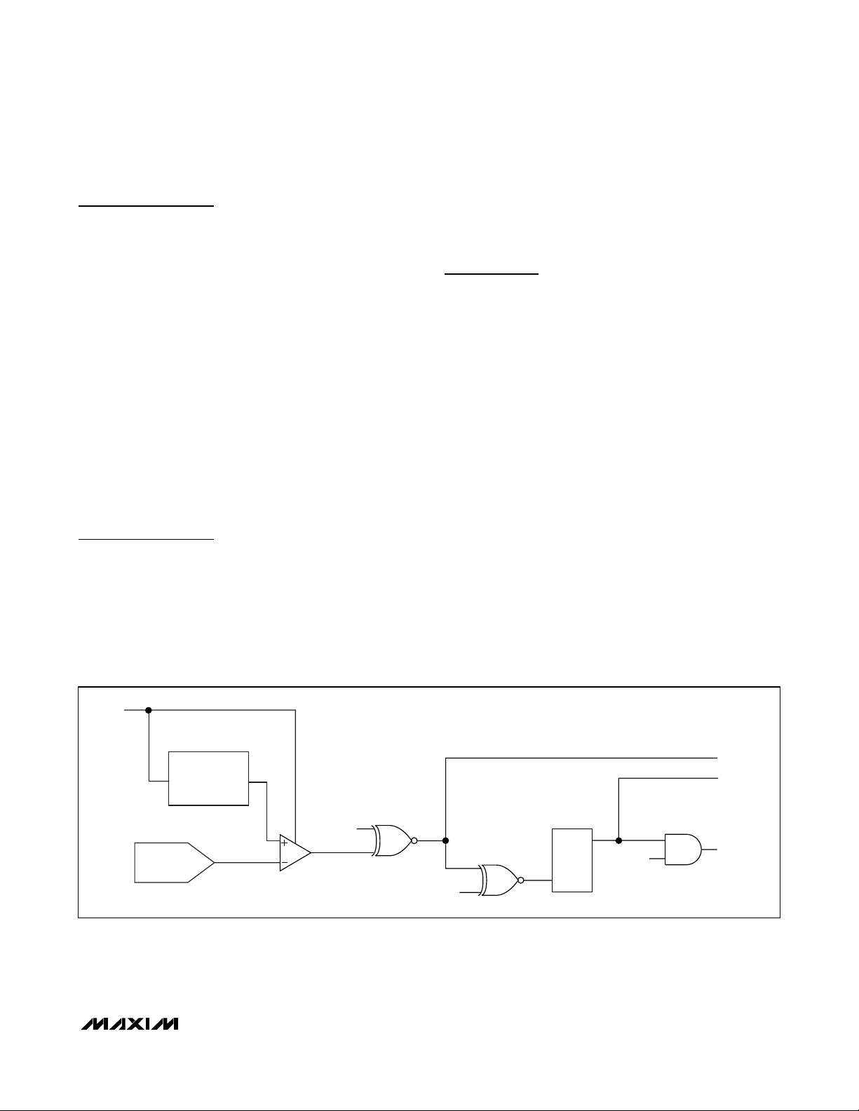
System Timing
The MAXQ3100 generates its internal system clock from
the external 32.768kHz crystal. This serves as the timebase for the RTC and is multiplied internally by a frequency-locked loop (FLL) to provide a system clock of
4.194MHz. Best performance is achieved when mated
with a 32.768kHz crystal rated for a 6pF load. No external load capacitors are required. The frequency accuracy of a crystal-based oscillator circuit is dependent upon
crystal accuracy, the match between the crystal and the
oscillator capacitor load, ambient temperature, etc.
A crystal warmup counter enhances operational reliability. Each time the external crystal oscillation must restart,
including a power-on reset, the device initiates a crystal
warmup period of approximately 2 seconds. This warmup
period allows time for the crystal amplitude and frequency to stabilize before using it as a clock source.
Power Management
Advanced power-management features minimize power
consumption by dynamically matching the processing
speed of the device to the required performance level.
This means device operation can be slowed and power
consumption minimized during periods of reduced
activity. When more processing power is required, the
microcontroller can increase its operating frequency.
Software-selectable clock-divide operations allow flexibility, selecting whether a system clock cycle (SYSCLK)
is 1, 2, 4, or 8 of the 4.194MHz oscillator cycles. By performing this function in software, a lower power state
can be entered without the cost of additional hardware.
For extremely power-sensitive applications, two additional low-power modes are available.
• Divide-by-256 power-management mode (PMM1)
(PMME = 1, CD1:0 = 00b)
• Stop mode (STOP = 1)
In PMM1, one system clock is 256 oscillator cycles, significantly reducing power consumption while the microcontroller functions at reduced speed. The optional
switchback feature allows enabled interrupt sources,
such as the external interrupts, to cause the processor to
quickly exit PMM1 mode and return to a faster internal
clock rate.
Figure 2. Clock Sources
POWER-ON
RESET
STOP
RESET
XDOG
STARTUP
TIMER
CLK INPUT
XDOG DONE
RESET DOG
WATCHDOG
TIMER
RWT
RESET
WATCHDOG RESET
WATCHDOG INTERRUPT
MAXQ3100
CLOCK
DIVIDER
DIV 1
DIV 2
SELECTOR
MUX
GLITCH-FREE
DIV 4
DIV 8
PWM1
DEFAULT
32kHz
CRYSTAL
OSCILLATOR
INPUT
FREQUENCY-
LOCKED LOOP
ENABLE
X32RY
FLLRY
4-CYCLE
DELAY
ENABLE
CLOCK
GENERATION
WATCHDOG DONE
STOP
POWER-ON
RESET
SYSTEM CLOCK
SWB
SWITCHBACK SOURCE
RESET
STOP

MAXQ3100
Mixed-Signal Microcontroller with Analog
Comparators, LCD, and RTC
______________________________________________________________________________________ 21
Power consumption reaches its minimum in stop mode.
In this mode, the system clock and all code execution
is halted. Upon receiving one of the following enabled
events, the device executes a 250ms warmup delay
and then begins normal operation from the point in the
code following the setting of the STOP bit:
• An enabled external interrupt pin is triggered.
• An enabled comparator interrupt is triggered.
• An external reset signal is applied to the RESET pin.
• The RTC time-of-day or subsecond alarms are
activated.
The following peripherals can be enabled during stop
mode:
• Analog comparators
• RTC
• LCD controller
Interrupts
Multiple interrupt sources are available for quick
response to internal and external events. The MAXQ
architecture uses a single interrupt vector (IV), single
interrupt-service routine (ISR) design. For maximum
flexibility, interrupts can be enabled globally, individually, or by module. When an interrupt condition occurs,
its individual flag is set, even if the interrupt source is
disabled at the local, module, or global level. Interrupt
flags must be cleared within the user-interrupt routine
to avoid repeated interrupts from the same source.
Application software must ensure a delay between the
write to the flag and the RETI instruction to allow time
for the interrupt hardware to remove the internal interrupt condition. Asynchronous interrupt flags require a
one-instruction delay, and synchronous interrupt flags
require a two-instruction delay.
When an enabled interrupt is detected, software jumps
to a user-programmable interrupt vector location. The
IV register defaults to 0000h on reset or power-up, so if
it is not changed to a different address, the user program must determine whether a jump to 0000h came
from a reset or interrupt source.
Once software control has been transferred to the ISR,
the interrupt identification register (IIR) can determine if
a system register or peripheral register was the source
of the interrupt. The specified module can then be interrogated for the specific interrupt source and software
can take appropriate action. Because the interrupts are
evaluated by user software, the user can define a
unique interrupt priority scheme for each application.
The following interrupt sources are available.
• Watchdog Interrupt
• External Interrupts 0 to 11
• Analog Comparator 0 and 1 Interrupts
• Temperature Sensor Interrupt
• RTC Time-of-Day and Subsecond Alarms
• Serial Port 0 Receive and Transmit Interrupts
• Serial Port 1 Receive and Transmit Interrupts
• Timer 0 Overflow Interrupt
• Timer 1 Overflow and External Trigger Interrupts
• Timer 2 Low Compare, Low Overflow, Capture/
Compare, and Overflow Interrupts
Reset Sources
Several reset sources are provided for microcontroller
control. Although code execution is halted in the reset
state, the high-frequency oscillator continues to oscillate.
Power-On Reset/Brownout Reset
An internal power-on reset circuit enhances system reliability. This circuit forces the device to perform a
power-on reset whenever a rising voltage on DV
DD
climbs above approximately V
RST
. Additionally, the
device performs a brownout reset whenever DV
DD
drops below V
RST
, a feature that can be optionally disabled in stop mode. The following events occur during
a power-on reset:
• All registers and circuits enter their power-on reset
state.
• I/O pins revert to their reset state, with logic one
states tracking DVDD.
• The power-on reset flag is set to indicate the source
of the reset.
• Code execution begins at location 8000h following a
2-second 32.768kHz warmup.
Watchdog Timer Reset
The watchdog timer functions are described in the
MAXQ Family User’s Guide
. Software can determine if
a reset was caused by a watchdog timeout by checking the watchdog timer reset flag (WTRF) in the WDCN
register. Execution resumes at location 8000h following
a watchdog timer reset.
External System Reset
Asserting the external RESET pin low causes the
device to enter the reset state. The external reset functions as described in the
MAXQ Family User’s Guide
.
Execution resumes at location 8000h after the RESET
pin is released.

MAXQ3100
Mixed-Signal Microcontroller with Analog
Comparators, LCD, and RTC
22 ______________________________________________________________________________________
I/O Ports
The microcontroller uses the Type C and Type D bidirectional I/O ports described in the
MAXQ Family
User’s Guide
. The use of two port types allows for maximum flexibility when interfacing to external peripherals.
Each port has independent, general-purpose I/O pins
and three configure/control registers. Many pins support alternate functions such as timers or interrupts,
which are enabled, controlled, and monitored by dedicated peripheral registers. Using the alternate function
automatically converts the pin to that function.
Type C port pins have Schmitt Trigger receivers and
full CMOS output drivers, and can support alternate
functions. The pin is either tri-stated or a weak pullup
when defined as an input, dependent on the state of
the corresponding bit in the output register.
Type D port pins have Schmitt Trigger receivers and
full CMOS output drivers, and can support alternate
functions. The pin is either tri-stated or a weak pullup
when defined as an input, dependent on the state of
the corresponding bit in the output register. All Type D
pins also have interrupt capability.
Figure 3. Type C/D Port Pin Schematic
PD.x
SF DIRECTION
SF ENABLE
PO.x
SF OUTPUT
MUXMUX
DV
DD
WEAK
DV
DD
MAXQ3100
I/O PAD
PORT PIN
PI.x OR SF INPUT
INTERRUPT
FLAG
FLAG
DETECT
CIRCUIT
EIES.x
TYPE D PORT ONLY

MAXQ3100
Mixed-Signal Microcontroller with Analog
Comparators, LCD, and RTC
______________________________________________________________________________________ 23
Real-Time Clock
A binary real-time clock keeps the time of day in
absolute seconds with 1/256-second resolution. The
32-bit second counter can count up to approximately
136 years and be translated to calendar format by the
application software. A time-of-day alarm and independent subsecond alarm can cause an interrupt or wake
the device from stop mode.
The independent subsecond alarm runs from the same
RTC, and allows the application to perform periodic
interrupts up to 8 seconds with a granularity of approximately 3.9ms. This creates an additional timer that can
be used to measure long periods without performance
degradations. Traditionally, long time periods have
been measured using multiple interrupts from shorter
programmable timers. Each timer interrupt required
servicing, with each accompanying interruption slowing
system operation. By using the RTC subsecond timer
as a long-period timer, only one interrupt is needed,
eliminating the performance hit associated with using a
shorter timer.
Higher accuracy can be obtained by using the useraccessible digital RTC trim function. This feature allows
the designer to fine tune the RTC timing to compensate
for crystal inaccuracies and any unintended boardlevel effects that could cause crystal-frequency drift.
The user can enable a 1Hz or 512Hz square-wave output on P3.4. Frequency measurements of these signals
can show if there is any deviation from the expected
frequency, and writes to the RTC trim register can compensate in increments of 1 to 127 steps, with each step
approximately 3.05ppm (30.5µs).
If the V
BAT
pin is not directly tied to the DVDDpin, then
there may be a short increase in IDDwhile the device is
switching between V
BAT
and DVDDas the RTC power
source. IDDcan temporarily increase up to 300µA while
DVDDis rising and in the range 1.05 x V
BAT
< DVDD<
[(1.05 x V
BAT
) + 200mV]. A similar effect may be
observed while V
BAT
is falling and in the range [(0.95 x
DVDD) - 200mV] < V
BAT
< 0.95 x DVDD.
Programmable Timers
The MAXQ3100 incorporates one instance each of the
timer 0, timer 1, and timer 2 peripherals. These timers
can be used in counter/timer/capture/compare/PWM
functions, allowing precise control of internal and external events. Timer 2 supports optional single-shot, external gating, and polarity control options as well as
carrier generation support for infrared transmit/receive
functions using serial port 0.
Timer 0
The timer 0 peripheral includes the following:
• 8-bit autoreload timer/counter
• 13-bit or 16-bit timer/counter
• Dual 8-bit timer/counter
• External pulse counter
Timer 1
The timer 1 peripheral includes the following:
• 16-bit autoreload timer/counter
• 16-bit capture
• 16-bit counter
• Clock generation output
Timer 2
The timer 2 peripheral includes the following:
• 16-bit autoreload timer/counter
• 16-bit capture
• 16-bit counter
• 8-bit capture and 8-bit timer
• 8-bit counter and 8-bit timer
• Infrared carrier generation support
Watchdog Timer
An internal watchdog timer greatly increases system
reliability. The timer resets the processor if software
execution is disturbed. The watchdog timer is a freerunning counter designed to be periodically reset by
the application software. If software is operating correctly, the counter is periodically reset and never
reaches its maximum count. However, if software operation is interrupted, the timer does not reset, triggering
a system reset and optionally a watchdog timer interrupt. This protects the system against electrical noise
or electrostatic discharge (ESD) upsets that could
cause uncontrolled processor operation. The internal
watchdog timer is an upgrade to older designs with
external watchdog devices, reducing system cost and
simultaneously increasing reliability.
The watchdog timer is controlled through bits in the
WDCN register. Its timeout period can be set to one of
four programmable intervals ranging from 212to 2
21
system clocks in its default mode, allowing flexibility to
support different types of applications. The interrupt
occurs 512 system clocks before the reset, allowing the
system to execute an interrupt and place the system in
a known, safe state before the device performs a total
system reset. At 4.194MHz, watchdog timeout periods
can be programmed from 976µs to 128s, depending on
the system clock mode.
MAXQ3100
Mixed-Signal Microcontroller with Analog
Comparators, LCD, and RTC
24 ______________________________________________________________________________________
In-Circuit Debug
Embedded debugging capability is available through
the debug port TAP. Embedded debug hardware and
embedded ROM firmware provide in-circuit debugging
capability to the user application, eliminating the need
for an expensive in-circuit emulator. Figure 4 shows a
block diagram of the in-circuit debugger. The in-circuit
debug features include:
• Hardware debug engine
• Set of registers able to set breakpoints on register,
code, or data accesses
• Set of debug service routines stored in the utility
ROM
The embedded hardware debug engine is an independent hardware block in the microcontroller. The debug
engine can monitor internal activities and interact with
selected internal registers while the CPU is executing
user code. Collectively, the hardware and software features allow two basic modes of in-circuit debugging:
• Background mode allows the host to configure and set
up the in-circuit debugger while the CPU continues to
execute the application software at full speed. Debug
mode can be invoked from background mode.
• Debug mode allows the debug engine to take control
of the CPU, providing read/write access to internal registers and memory, and single-step trace operation.
Serial Peripherals
The MAXQ3100 incorporates two 8051-style universal
synchronous/asynchronous receiver/transmitters. The
USARTs allow the device to conveniently communicate
with other RS-232 interface-enabled devices, as well as
PCs and serial modems when paired with an external
RS-232 line driver/receiver. The dual independent
USARTs can communicate simultaneously at different
baud rates with two separate peripherals. The USART
can detect framing errors and indicate the condition
through a user-accessible software bit.
The time base of the serial ports is derived from either a
division of the system clock or the dedicated baud
clock generator. The following table summarizes the
operating characteristics as well as the maximum baud
rate of each mode.
Serial port 0 contains additional functionality to support
low-speed infrared transmission in combination with the
PWM function of timer 2. When enabled in this mode,
the serial port automatically outputs a waveform generated by combining the normal serial port output waveform with the PWM carrier waveform output by timer 2,
using a logical OR or logical NOR function. The output
of serial port 0 in this mode can be used to drive an
infrared LED to communicate using a fixed-frequency
carrier modulated signal. Depending on the drive
strength required, the output may require a buffer when
used for this purpose.
Figure 4. In-Circuit Debugger
MAXQ3100
TMS
TCK
TDI
TDO
TAP
CONTROLLER
DEBUG
SERVICE
ROUTINES
(UTILITY ROM)
DEBUG
ENGINE
CONTROL
BREAKPOINT
ADDRESS
CPU
DATA
MODE TYPE START BITS DATA BITS STOP BIT MAX BAUD RATE AT 4.194MHz
Mode 0 Synchronous — 8 — 1.05Mbps
Mode 1 Asynchronous 1 8 1 131kbps
Mode 2 Asynchronous 1 8 + 1 1 131kbps
Mode 3 Asynchronous 1 8 + 1 1 131kbps
MAXQ3100
Mixed-Signal Microcontroller with Analog
Comparators, LCD, and RTC
______________________________________________________________________________________ 25
Analog Comparators
The MAXQ3100 incorporates a pair of 1-bit analog-todigital comparators. The comparator inputs can be
connected to a wide range of peripherals, including
chemical, motion, or proximity detectors; voltage-supply monitoring; or any other appropriate analog input.
The comparator measures the analog inputs against
the internal +1.25V reference. The polarity of the internal comparator-output signal can be selected to indicate a value above or below the internal reference. The
comparators can be configured to generate an optional
interrupt in addition to setting an internal flag when the
input is out of range. A combination of the two comparators along with appropriate biasing of an input
allows the two comparators to be used as a window
comparator. When not in use, the pins associated with
the comparator are usable as general-purpose I/O. A
useful feature of the comparators is that they can be
used to wake the device from stop mode, allowing the
device to monitor external voltages while in an ultralow-power mode and only wake when necessary.
Temperature Sensor
The internal temperature sensor has a user-selectable
resolution of 10 (0.5°C), 11 (0.25°C), 12 (0.125°C), or
13 (0.0625°C) bits. Higher resolutions require longer
conversion times.
Setting the START bit initiates the temperature conversion, and the temperature sensor hardware clears the
bit when the conversion is complete. This bit can be
polled by software, or, optionally, the temperature conversion complete interrupt can be used to alert the system that the results are ready to be read from the
temperature results register (TEMPR).
Applications Information
Grounds and Bypassing
Careful PC-board layout significantly minimizes
crosstalk among the comparator inputs and other digital
signals. Keep digital and analog lines separate, and use
ground traces as shields between them where possible.
Bypass DV
DD
with a capacitor as low as 1µF and keep
bypass capacitor leads short for best noise rejection.
This device incorporates both analog and digital components, straddling both the analog and digital ground
planes. For increased accuracy, an LC filter can be
used to isolate pin 59. This pin powers the analog circuitry, and the additional filtering reduces the noise
entering the analog block.
Device Applications
The low-power, high-performance RISC architecture of
the MAXQ3100 makes it an excellent fit for many applications that require analog measurements combined
with the intelligence of a full-featured microcontroller.
Simple voltage-dividers can be used to scale any input
into a value in the range of the +1.25V reference. The
dual comparators allow the device to function as a simple limit comparator or window comparator in a wide
range of analog applications.
Figure 5. Analog Comparator Functional Diagram
CMON
INTERNAL
1.25V
REFERENCE
CMPOL
CMPx
CMM
SET
CMO
CMF
Q
CMM
INTERRUPT
REQUEST

MAXQ3100
Mixed-Signal Microcontroller with Analog
Comparators, LCD, and RTC
26 ______________________________________________________________________________________
Additional Documentation
Designers must have four documents to fully use all the
features of this device. This data sheet contains pin
descriptions, feature overviews, and electrical specifications. Errata sheets contain deviations from published specifications. The user’s guides offer detailed
information about programming, device features, and
operation. The following documents can be downloaded from www.maxim-ic.com/microcontrollers.
• The MAXQ3100 data sheet, which contains electrical/timing specifications and pin descriptions, available at www.maxim-ic.com/MAXQ3100
.
• The MAXQ3100 errata sheet, available at
www.maxim-ic.com/errata.
• The
MAXQ Family User’s Guide
, which contains
detailed information on core features and operation,
including programming, avaliable at www.maximic.com/MAXQUG.
• The
MAXQ Family User’s Guide: MAXQ3100
Supplement
, which contains detailed information on
features specific to the MAXQ3100, available at
www.maxim-ic.com/MAXQ3100UG.
Development and Technical Support
A variety of highly versatile, affordably priced development tools for this microcontroller are available from
Maxim/Dallas Semiconductor and third-party suppliers,
including:
• Compilers
• In-circuit emulators
• Integrated development environments (IDEs)
• JTAG-to-serial converters for programming and
debugging
A partial list of development tool vendors can be found
on our website at www.maxim-ic.com/microcontrollers
.
Technical support is available through email at
maxq.support@dalsemi.com.

MAXQ3100
Mixed-Signal Microcontroller with Analog
Comparators, LCD, and RTC
______________________________________________________________________________________ 27
Typical Application Circuits
Typical Application Circuit #1
Typical Application Circuit #1
shows a general-purpose
implementation using a MAXQ3100 that reads two sensor inputs, displays result and status information on an
LCD display, and also interfaces simultaneously with
an RS-232 and RS-485 networks. I/O pins that are not
dedicated to special functions are available to control
other system functions.
3.3V
DIRECT INPUT
FROM USER-
DEFINED SENSOR
SCALED
COMPARATOR
INPUT
R
1
R
2
DV
CMP0
CMP1
BACKUP BATTERY
VBAT
DD
V
REF
MAXQ3100
TXD0
RXD0
TXD1
RXD1
Px.x
SEG[39:0]
COM[3:0]
RS-232
Tx/Rx
RS-485
Tx/Rx
RTS
LCD MODULE
NOTE THAT UP TO 160 LCD SEGMENTS
CAN BE DRIVEN IF OTHER MUXED PIN
FUNCTIONS ARE NOT USED.
2
C FRAM
I
OR EEPROM
JTAG DOWNLOAD/
DEBUG
CONNECTOR
P2.3
P2.2
TDO
TDI
TCK
TMS
32KIN
32KOUT
GENERAL-
PURPOSE I/O
INT7
INT6
BUTTON 1
BUTTON 2

MAXQ3100
Mixed-Signal Microcontroller with Analog
Comparators, LCD, and RTC
28 ______________________________________________________________________________________
Typical Application Circuits (continued)
Typical Application Circuit #2
Another target application of the MAXQ3100 is in the
electricity metering market. When coupled with an analog front-end, the microcontroller becomes the core of
an affordable electricity metering solution. Such an
application can accurately keep time, incorporate a
versatile display, and allow for multiple modes of communication. See
Typical Application Circuit #2
.
UNREGULATED
SUPPLY
ENERGY
METERING IC
CALIBRATION
EQUIPMENT
REGULATOR
3.3V
BACKUP BATTERY
ISOLATION
DV
CMP0
V
BAT
CMP1
T0
SQW
DD
MAXQ3100
V
REF
IR Tx/Rx
CIRCUIT
TXD0
RXD0
TXD1
RXD1
RS-232
Tx/Rx
IR Rx
MODULE
2
C FRAM
I
OR EEPROM
JTAG DOWNLOAD/
DEBUG
CONNECTOR
P2.3
P2.2
TDO
TDI
TCK
TMS
32KIN
32KOUT
SEG[39:0]
COM[3:0]
INT7
INT6
LCD MODULE
NOTE THAT UP TO 160 LCD SEGMENTS
CAN BE DRIVEN IF OTHER MUXED PIN
FUNCTIONS ARE NOT USED.
BUTTON 1
BUTTON 2
MAXQ3100
Mixed-Signal Microcontroller with Analog
Comparators, LCD, and RTC
______________________________________________________________________________________ 29
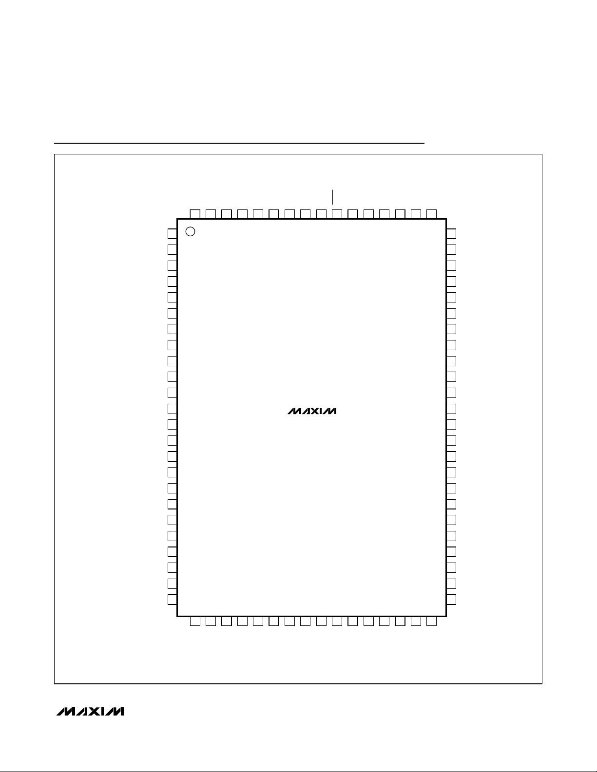
Pin Configuration
TOP VIEW
DGND
P0.4/INT4/T1
P0.5/INT5/T1EX
P0.6/INT6
P0.7/INT7
DV
COM0
COM1
COM2
COM3
DGND
SEG0
SEG1
SEG2
SEG3
SEG4
SEG5
SEG6
SEG7
SEG8
SEG9
SEG10
SEG11
SEG12
DD
DGND
P0.3/INT3/T0
P0.2/INT2/T0G
P0.1/INT1/RXD0
P0.0/INT0/TXD0
DV
77
80
1
2
3
4
5
6
DD
7
8
9
10
11
12
13
14
15
16
17
18
19
20
21
22
23
24
78
79
76
32KOUT
74
75
32KIN
73
MAXQ3100
BAT
V
72
RESET
71
P3.6/CMP1
P3.5/CMP0
70
69
P3.4/SQW
P3.3/TMS
68
67
P3.1/TDO
P3.2/TCK
65
66
64
P3.0/TDI
63
P1.3/INT11/RXD1
P1.2/INT10/TXD1
62
61
P1.1/INTP/T2A
P1.0/INT8/T2B
60
DV
59
DD
DGND
58
V
57
ADJ
56
V
LCD2
V
55
LCD1
54
V
LCD
DV
53
DD
DGND
52
51
P2.7/SEG39
P2.6/SEG38
50
49
P2.5/SEG37
48
P2.4/SEG36
P2.3/SEG35
47
P2.2/SEG34
46
P2.1/SEG33
45
44
P2.0/SEG32
SEG31
43
SEG30
42
SEG29
41
25
SEG13
26
SEG14
27
SEG15
28
SEG16
29
SEG17
30
SEG18
SEG19
32
SEG20
33
SEG21
34
SEG22
35
SEG23
36
SEG24
37
SEG25
38
SEG26
39
SEG27
40
SEG28
31
MQFP
MAXQ3100
Mixed-Signal Microcontroller with Analog
Comparators, LCD, and RTC
Maxim cannot assume responsibility for use of any circuitry other than circuitry entirely embodied in a Maxim product. No circuit patent licenses are
implied. Maxim reserves the right to change the circuitry and specifications without notice at any time.
30
____________________Maxim Integrated Products, 120 San Gabriel Drive, Sunnyvale, CA 94086 408-737-7600
© 2007 Maxim Integrated Products is a registered trademark of Maxim Integrated Products, Inc.
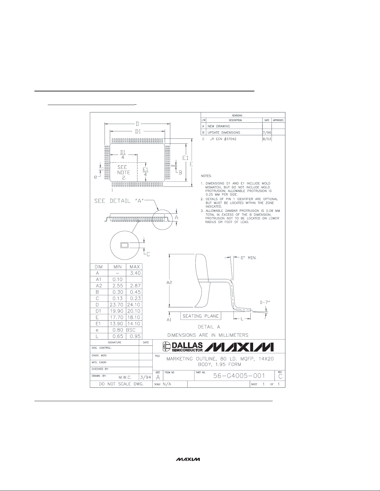
Package Information
(The package drawing(s) in this data sheet may not reflect the most current specifications. For the latest package outline information,
go to www.maxim-ic.com/DallasPackInfo
)
.
Revision History
Rev 0; 6/07: Original release.
 Loading...