

Page 1
General Description
The MAX9994 high-linearity downconversion mixer provides 8.3dB gain, +26.2dBm IIP3, and 9.7dB NF for
1400MHz to 2200MHz UMTS/WCDMA, DCS, and PCS
base-station receiver applications. With a wide LO range
of 1400MHz to 2000MHz, the MAX9994 can be used in
either high-side or low-side LO injection architectures,
depending on the RF band of interest. Higher LO applications are supported by the MAX9996, which is pin-pin
and functionally compatible with the MAX9994.
In addition to offering excellent linearity and noise performance, the MAX9994 also yields a high level of component integration. This device includes a doublebalanced passive mixer core, an IF amplifier, a dualinput LO selectable switch, and an LO buffer. On-chip
baluns are also integrated to allow for single-ended RF
and LO inputs. The MAX9994 requires a nominal LO
drive of 0dBm, and supply current is guaranteed to be
below 235mA.
The MAX9994/MAX9996 are pin compatible with the
MAX9984/MAX9986 815MHz to 995MHz mixers, making this entire family of downconverters ideal for applications where a common PC board layout is used for
both frequency bands. The MAX9994 is also functionally compatible with the MAX9993.
The MAX9994 is available in a compact, 20-pin, thin
QFN package (5mm x 5mm) with an exposed pad.
Electrical performance is guaranteed over the extended
-40°C to +85°C temperature range.
Applications
UMTS/LTE Base Stations
TD-SCDMA/TD-LTE Base Stations
DCS1800/PCS1900 EDGE Base Stations
cdmaOne™ and cdma2000
®
Base Stations
PHS/PAS Base Stations
Predistortion Receivers
Fixed Broadband Wireless Access
Wireless Local Loop
Private Mobile Radios
Military Systems
Microwave Links
Digital and Spread-Spectrum Communication
Systems
Features
♦ 1400MHz to 2200MHz RF Frequency Range
♦ 1400MHz to 2000MHz LO Frequency Range
(MAX9994)
♦ 1900MHz to 2400MHz LO Frequency Range
(MAX9996)
♦ 40MHz to 350MHz IF Frequency Range
♦ 8.3dB Conversion Gain
♦ +26.2dBm Input IP3
♦ +12.6dBm Input 1dB Compression Point
♦ 9.7dB Noise Figure
♦ 67dBc 2RF - 2LO Spurious Rejection at
P
RF
= -10dBm
♦ Integrated LO Buffer
♦ Integrated RF and LO Baluns for Single-Ended
Inputs
♦ Low -3dBm to +3dBm LO Drive
♦ Built-In SPDT LO Switch with 45dB LO1 to LO2
Isolation and 50ns Switching Time
♦ Pin Compatible with the MAX9984/MAX9986
815MHz to 995MHz Mixers
♦ Functionally Compatible with the MAX9993
♦ External Current-Setting Resistors Provide Option
for Operating Mixer in Reduced Power/Reduced
Performance Mode
MAX9994
SiGe High-Linearity, 1400MHz to 2200MHz
Downconversion Mixer with LO Buffer/Switch
________________________________________________________________
Maxim Integrated Products
1
Pin Configuration/Functional Diagram and Typical
Application Circuit appear at end of data sheet.
19-3435; Rev 1; 12/10
For pricing, delivery, and ordering information, please contact Maxim Direct at 1-888-629-4642,
or visit Maxim’s website at www.maxim-ic.com.
EVALUATION KIT
AVAILABLE
Ordering Information
**
EP = Exposed pad.
+
Denotes a lead(Pb)-free/RoHS-compliant package.
T = Tape and reel.
cdma2000 is a registered trademark of Telecommunications
Industry Association.
cdmaOne is a trademark of CDMA Development Group.
PART TEMP RANGE PIN-PACKAGE
MAX9994ETP+ -40°C to +85°C
MAX9994ETP+T -40°C to +85°C
20 Thin QFN-EP**
5mm 5mm
bulk
20 Thin QFN-EP**
5mm 5mm
T/R
Page 2
MAX9994
SiGe High-Linearity, 1400MHz to 2200MHz
Downconversion Mixer with LO Buffer/Switch
2 _______________________________________________________________________________________
ABSOLUTE MAXIMUM RATINGS
DC ELECTRICAL CHARACTERISTICS
(
Typical Application Circuit
, VCC= +4.75V to +5.25V, no RF signal applied, IF+ and IF- outputs pulled up to VCCthrough inductive
chokes, R
1
= 806Ω, R2= 549Ω, TC= -40°C to +85°C, unless otherwise noted. Typical values are at VCC= +5V, TC= +25°C, unless
otherwise noted.)
Stresses beyond those listed under “Absolute Maximum Ratings” may cause permanent damage to the device. These are stress ratings only, and functional
operation of the device at these or any other conditions beyond those indicated in the operational sections of the specifications is not implied. Exposure to
absolute maximum rating conditions for extended periods may affect device reliability.
VCCto GND...........................................................-0.3V to +5.5V
IF+, IF-, LOBIAS, LOSEL, IFBIAS to GND...-0.3V to (V
CC
+ 0.3V)
TAP ........................................................................-0.3V to +1.4V
LO1, LO2, LEXT to GND........................................-0.3V to +0.3V
RF, LO1, LO2 Input Power .............................................+12dBm
RF (RF is DC shorted to GND through a balun) .................50mA
Continuous Power Dissipation (T
A
= +70°C)
20-Pin Thin QFN-EP (derate 20mW/°C above +70°C)..............1.8W
θ
JA
(Note 1) ...................................................................+38°C/W
θ
JC
(Note 1) .....................................................................+8°C/W
Operating Temperature Range (Note 2).....T
C
= -40°C to +85°C
Junction Temperature......................................................+150°C
Storage Temperature Range .............................-65°C to +150°C
Lead Temperature (soldering 10s) ..................................+300°C
Soldering Temperature (reflow) .......................................+260°C
Note 1: Package thermal resistances were obtained using the method described in JEDEC specification JESD51-7, using a four-layer
board. For detailed information on package thermal considerations, refer to www.maxim-ic.com/thermal-tutorial
.
Note 2: T
C
is the temperature on the exposed pad of the package.
RECOMMENDED AC OPERATING CONDITIONS
Supply Voltage V
Supply Current I
LO_SEL Input Logic-Low V
LO_SEL Input Logic-High V
PARAMETER SYMBOL CONDITIONS MIN TYP MAX UNITS
CC
CC
IL
IH
4.75 5.00 5.25 V
2V
206 235 mA
0.8 V
PARAMETER SYMBOL CONDITIONS MIN TYP MAX UNITS
RF Frequency Range f
LO Frequency Range f
IF Frequency Range f
LO Drive Level P
RF
LO
IF
LO
(Note 3) 1400 2200 MHz
(Note 3) 1400 2000 MHz
(Note 3) 40 350 MHz
(Note 3) -3 +3 dBm
Page 3
MAX9994
SiGe High-Linearity, 1400MHz to 2200MHz
Downconversion Mixer with LO Buffer/Switch
_______________________________________________________________________________________ 3
AC ELECTRICAL CHARACTERISTICS—fRF= 1700MHz TO 2200MHz, LOW-SIDE LO INJECTION
(
Typical Application Circuit
, VCC= +4.75V to +5.25V, RF and LO ports are driven from 50Ω sources, PLO= -3dBm to +3dBm,
P
RF
= -5dBm, fRF= 1700MHz to 2200MHz, fLO= 1400MHz to 2000MHz, fIF= 200MHz, fRF> fLO, TC= -40°C to +85°C, unless other-
wise noted. Typical values are at V
CC
= +5V, P
RF
= -5dBm, PLO= 0dBm, fRF= 1900MHz, fLO= 1700MHz, fIF= 200MHz,
T
C
= +25°C, unless otherwise noted.) (Notes 4, 5)
Conversion Gain GC P
Gain Variation Over Temperature TC = -40°C to +85°C ±0.75 dB
Input Compres sion Point P
Input Third-Order Intercept Point
(Note 6)
Input IP3 Variation Over
Temperature
Noise Figure NF Single sideband 9.7 dB
Noise Figure Under-Blocking
LO Drive -3 +3 dBm
Spurious Response at IF
LO1 to LO2 Isolation
(Note 4)
Max imum LO Leakage at RF
Port
Max imum LO Lea kage at IF Port PLO = +3dBm -30 dBm
Min imum RF-to-IF Isolation 35 dB
LO Switching Time 50% of LOSEL to IF settled to within 2° 50 ns
RF Port Return Loss 21 dB
LO Port Return Loss
IF Port Return Loss
PARAMETER S YMBOL CONDITIONS MIN TYP MAX UNITS
(Note 7) 12.6 dBm
1dB
IIP3
T
2 x 2 2RF - 2LO
3 x 3 3RF - 3LO
P
< +2dBm, TA = +25°C (Note 6) 7.2 8.3 9.2 dB
RF
Two tones:
f
= 2000MHz, f
RF1
= -5dBm/tone, fLO = 1800MHz,
P
RF
P
= 0dBm, TA = +25°C
LO
= -40°C to +85°C ±0.5 dB
C
P
= 5dBm, f
RF
f
= 1810MHz, f
LO
LO2 selected,
1500MHz < f
LO1 selected,
1500MHz < f
= +3dBm -17 dBm
LO
LO1/2 port selected,
LO2/1 and IF terminated
LO1/2 port unselected,
LO2/1 and IF terminated
LO driven at 0dBm, RF terminated into
50, differential 200
LO
LO
= 2001MHz,
RF2
= 2000MHz,
RF
= 2100MHz (Note 8)
block
PRF = -10dBm 67
P
PRF = -10dBm 82
P
< 1700MHz
< 1700MHz
23.5 26.2 dBm
19 dB
= -5dBm 62
RF
= -5dBm 72
RF
40 52
40 45
16
26
20 dB
dBc
dB
dB
Page 4
MAX9994
SiGe High-Linearity, 1400MHz to 2200MHz
Downconversion Mixer with LO Buffer/Switch
4 _______________________________________________________________________________________
Note 3: Operation outside this range is possible, but with degraded performance of some parameters.
Note 4: Guaranteed by design and characterization.
Note 5: All limits include external component losses. Output measurements taken at IF output of the
Typical Application Circuit
.
Note 6: Production tested.
Note 7: Compression point characterized. It is advisable not to operate continuously the mixer RF input above +12dBm.
Note 8: Measured with external LO source noise filtered so the noise floor is -174dBm/Hz. This specification reflects the effects of all
SNR degradations in the mixer, including the LO noise as defined in Application Note 2021:
Specifications and
Measurement of Local Oscillator Noise in Integrated Circuit Base Station Mixers
.
AC ELECTRICAL CHARACTERISTICS—fRF= 1455MHz, HIGH-SIDE LO INJECTION
(
Typical Application Circuit
, RF and LO ports are driven from 50Ω sources, fRF< fLO, VCC= +5V, PRF= -5dBm, PLO= 0dBm,
f
RF
= 1455MHz, fLO= 1625MHz, fIF= 170MHz, TC= +25°C, LO2 is selected, unless otherwise noted.) (Note 5)
AC ELECTRICAL CHARACTERISTICS—fRF= 1500MHz, HIGH-SIDE LO INJECTION
(
Typical Application Circuit
, RF and LO ports are driven from 50Ω sources, fRF< fLO, VCC= +5V, PRF= -5dBm, PLO= 0dBm,
f
RF
= 1500MHz, fLO= 1650MHz, fIF= 150MHz, TC= +25°C, LO1 is selected, unless otherwise noted.) (Note 5)
Conversion Gain GC 8.8 dB
Input Third-Order Intercept Point IIP3
Input Compres sion Point
(Note 7)
2LO - 2RF Spurious Response 2 x 2
LO-to-IF Leakage LOSEL = LO2 -30.2 dBm
PARAMETER S YMBOL CONDITIONS MIN TYP MAX UNITS
Conversion Gain GC 8.9 dB
Input Third-Order Intercept Point IIP3
Input Compres sion Point
(Note 7)
2LO - 2RF Spurious Response 2 x 2
LO-to-IF Leakage -33.2 dBm
PARAMETER S YMBOL CONDITIONS MIN TYP MAX UNITS
Two tones:
f
= 1455MHz, f
RF1
= -5dBm/tone
P
RF
IP
12.7 dBm
1dB
PRF = -10dBm 71.4
= -5dBm 66.4
P
RF
Two tones:
f
= 1500MHz, f
RF1
= -5dBm/tone
P
RF
IP
12.5 dBm
1dB
PRF = -10dBm 70.4
= -5dBm 65.4
P
RF
= 1456MHz,
RF2
= 1501MHz,
RF2
25.6 dBm
25.5 dBm
dBc
dBc
Page 5
MAX9994
SiGe High-Linearity, 1400MHz to 2200MHz
Downconversion Mixer with LO Buffer/Switch
_______________________________________________________________________________________
5
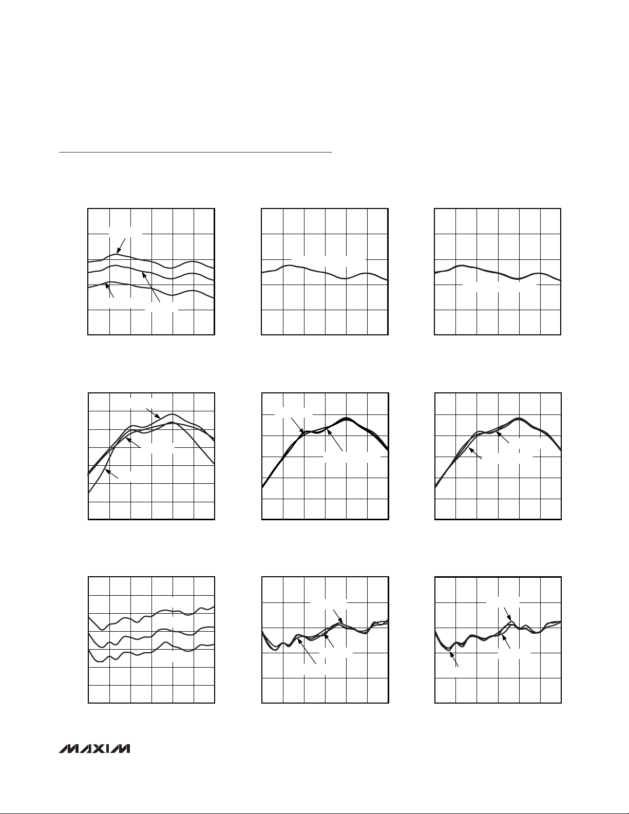
Typical Operating Characteristics
(MAX9994
Typical Application Circuit
, VCC= +5.0V, PLO= 0dBm, PRF= -5dBm, fRF= 1700MHz to 2200MHz, LO is Low-Side
Injected for a 200MHz IF, unless otherwise noted.)
CONVERSION GAIN vs. RF FREQUENCY
11
10
9
8
CONVERSION GAIN (dB)
7
6
TC = -25°C
TC = +85°C
1500 18001650 1950 2100 2250 2400
TC = +25°C
RF FREQUENCY (MHz)
MAX9994 toc01
CONVERSION GAIN (dB)
INPUT IP3 vs. RF FREQUENCY
28
27
26
25
24
INPUT IP3 (dBm)
23
22
21
1500 1800 19501650 2100 2250 2400
TC = +25°C
TC = -25°C
TC = +85°C
RF FREQUENCY (MHz)
MAX9994 toc04
INPUT IP3 (dBm)
CONVERSION GAIN vs. RF FREQUENCY
11
10
9
8
7
6
1500 18001650 1950 2100 2250 2400
28
27
26
25
24
23
22
1500 1800 19501650 2100 2250 2400
PLO = -3dBm, 0dBm, +3dBm
RF FREQUENCY (MHz)
INPUT IP3 vs. RF FREQUENCY
PLO = +3dBm
PLO = -3dBm, 0dBm
RF FREQUENCY (MHz)
11
MAX9994 toc02
10
9
8
CONVERSION GAIN (dB)
7
6
28
27
MAX9994 toc05
26
25
INPUT IP3 (dBm)
24
23
22
CONVERSION GAIN vs. RF FREQUENCY
MAX9994 toc03
VCC = 4.75V, 5.0V, 5.25V
1500 18001650 1950 2100 2250 2400
RF FREQUENCY (MHz)
INPUT IP3 vs. RF FREQUENCY
MAX9994 toc06
VCC = 4.75V
VCC = 5.0V, 5.25V
1500 1800 19501650 2100 2250 2400
RF FREQUENCY (MHz)
NOISE FIGURE vs. RF FREQUENCY
13
12
11
10
9
NOISE FIGURE (dB)
8
7
6
1500 1800 19501650 2100 2250 2400
RF FREQUENCY (MHz)
TC = +85°C
TC = +25°C
TC = -25°C
MAX9994 toc07
NOISE FIGURE vs. RF FREQUENCY
12
11
10
9
NOISE FIGURE (dB)
8
7
1500 1800 19501650 2100 2250 2400
PLO = -3dBm
PLO = 0dBm
PLO = +3dBm
RF FREQUENCY (MHz)
MAX9994 toc08
NOISE FIGURE (dB)
NOISE FIGURE vs. RF FREQUENCY
12
11
10
9
VCC = 5.0V
8
7
1500 1800 19501650 2100 2250 2400
VCC = 5.25V
VCC = 4.75V
RF FREQUENCY (MHz)
MAX9994 toc09
Page 6
MAX9994
SiGe High-Linearity, 1400MHz to 2200MHz
Downconversion Mixer with LO Buffer/Switch
6 _______________________________________________________________________________________
Typical Operating Characteristics (continued)
(MAX9994
Typical Application Circuit
, VCC= +5.0V, PLO= 0dBm, PRF= -5dBm, fRF= 1700MHz to 2200MHz, LO is Low-Side
Injected for a 200MHz IF, unless otherwise noted.)
2RF - 2LO RESPONSE vs. RF FREQUENCY
85
PRF = -5dBm
80
75
70
TC = +25°C
65
60
2RF - 2LO RESPONSE (dBc)
55
50
45
1500 1800 19501650 2100 2250 2400
TC = -25°C
TC = +85°C
RF FREQUENCY (MHz)
3RF - 3LO RESPONSE vs. RF FREQUENCY
95
PRF = -5dBm
90
85
80
75
70
65
3RF - 3LO RESPONSE (dBc)
TC = -25°C
60
55
1500 1800 19501650 2100 2250 2400
RF FREQUENCY (MHz)
TC = +85°C
TC = +25°C
2RF - 2LO RESPONSE vs. RF FREQUENCY
85
80
MAX9994 toc10
75
70
65
60
2RF - 2LO RESPONSE (dBc)
55
50
45
1500 1800 19501650 2100 2250 2400
3RF - 3LO RESPONSE vs. RF FREQUENCY
95
90
MAX9994 toc13
85
80
75
70
65
3RF - 3LO RESPONSE (dBc)
60
55
1500 1800 19501650 2100 2250 2400
PRF = -5dBm
PLO = +3dBm
PLO = -3dBm
RF FREQUENCY (MHz)
PRF = -5dBm
PLO = -3dBm, 0dBm, +3dBm
RF FREQUENCY (MHz)
PLO = 0dBm
2RF - 2LO RESPONSE vs. RF FREQUENCY
90
85
MAX9994 toc11
80
75
70
65
60
2RF - 2LO RESPONSE (dBc)
55
50
45
1500 1800 19501650 2100 2250 2400
3RF - 3LO RESPONSE vs. RF FREQUENCY
95
90
MAX9994 toc14
85
80
75
70
65
3RF - 3LO RESPONSE (dBc)
60
55
1500 1800 19501650 2100 2250 2400
PRF = -5dBm
VCC = 4.75V, 5.0V, 5.25V
RF FREQUENCY (MHz)
PRF = -5dBm
VCC = 5.25V
RF FREQUENCY (MHz)
VCC = 5.0V
VCC = 4.75V
MAX9994 toc12
MAX9994 toc15
INPUT P
15
14
13
(dBm)
1dB
12
INPUT P
TC = -25°C
11
10
1500 1800 19501650 2100 2250 2400
vs. RF FREQUENCY
1dB
TC = +85°C
TC = +25°C
RF FREQUENCY (MHz)
MAX9994 toc16
INPUT P
15
14
13
(dBm)
1dB
12
INPUT P
11
10
1500 1800 19501650 2100 2250 2400
vs. RF FREQUENCY
1dB
PLO = -3dBm, 0dBm, +3dBm
RF FREQUENCY (MHz)
MAX9994 toc17
(dBm)
1dB
INPUT P
INPUT P
15
14
13
12
VCC = 4.75V
11
10
1500 1800 19501650 2100 2250 2400
1dB
RF FREQUENCY (MHz)
vs. RF FREQUENCY
VCC = 5.25V
VCC = 5.0V
MAX9994 toc18
Page 7

MAX9994
SiGe High-Linearity, 1400MHz to 2200MHz
Downconversion Mixer with LO Buffer/Switch
_______________________________________________________________________________________
7
Typical Operating Characteristics (continued)
(MAX9994
Typical Application Circuit
, VCC= +5.0V, PLO= 0dBm, PRF= -5dBm, fRF= 1700MHz to 2200MHz, LO is Low-Side
Injected for a 200MHz IF, unless otherwise noted.)
LO SWITCH ISOLATION
vs. LO FREQUENCY
55
50
45
40
LO SWITCH ISOLATION (dB)
35
TC = +85°C
1300 1600 17501450 1900 2050 2200
LO FREQUENCY (MHz)
TC = -25°C
TC = +25°C
MAX9994 toc19
LO SWITCH ISOLATION (dB)
LO LEAKAGE AT IF PORT
vs. LO FREQUENCY
-20
-25
-30
-35
-40
-45
LO LEAKAGE (dBm)
-50
-55
-60
1300 1600 17501450 1900 2050 2200
TC = +85°C
TC = -25°C
TC = +25°C
LO FREQUENCY (MHz)
MAX9994 toc22
LO LEAKAGE (dBm)
LO SWITCH ISOLATION
vs. LO FREQUENCY
55
50
45
40
35
1300 1600 17501450 1900 2050 2200
PLO = +3dBm
PLO = -3dBm
PLO = 0dBm
LO FREQUENCY (MHz)
LO LEAKAGE AT IF PORT
vs. LO FREQUENCY
-20
-25
-30
-35
-40
-45
-50
-55
-60
1300 1600 17501450 1900 2050 2200
PLO = 0dBm
P
LO
LO FREQUENCY (MHz)
PLO = -3dBm
= +3dBm
55
MAX9994 toc20
50
45
LO SWITCH ISOLATION (dB)
40
35
1300 1600 17501450 1900 2050 2200
-20
-25
MAX9994 toc23
-30
-35
-40
LO LEAKAGE (dBm)
-45
-50
-55
1300 1600 17501450 1900 2050 2200
LO SWITCH ISOLATION
vs. LO FREQUENCY
VCC = 4.75V, 5.0V, 5.25V
LO FREQUENCY (MHz)
LO LEAKAGE AT IF PORT
vs. LO FREQUENCY
VCC = 5.25V
VCC = 5.0V
VCC = 4.75V
LO FREQUENCY (MHz)
MAX9994 toc21
MAX9994 toc24
LO LEAKAGE AT RF PORT
vs. LO FREQUENCY
-10
-15
-20
-25
LO LEAKAGE AT RF PORT (dBm)
-30
1300 1600 17501450 1900 2050 2200
TC = -25°C, +25°C, +85°C
LO FREQUENCY (MHz)
-10
MAX9994 toc25
-15
-20
PLO = -3dBm, 0dBm, +3dBm
-25
LO LEAKAGE AT RF PORT (dBm)
-30
1300 1600 17501450 1900 2050 2200
LO LEAKAGE AT RF PORT
vs. LO FREQUENCY
LO FREQUENCY (MHz)
-10
MAX9994 toc26
-15
-20
VCC = 4.75V
-25
LO LEAKAGE AT RF PORT (dBm)
-30
1300 1600 17501450 1900 2050 2200
LO LEAKAGE AT RF PORT
vs. LO FREQUENCY
MAX9994 toc27
VCC = 5.0V
VCC = 5.25V
LO FREQUENCY (MHz)
Page 8

MAX9994
SiGe High-Linearity, 1400MHz to 2200MHz
Downconversion Mixer with LO Buffer/Switch
8 _______________________________________________________________________________________
Typical Operating Characteristics (continued)
(MAX9994
Typical Application Circuit
, VCC= +5.0V, PLO= 0dBm, PRF= -5dBm, fRF= 1700MHz to 2200MHz, LO is Low-Side
Injected for a 200MHz IF, unless otherwise noted.)
RF-TO-IF ISOLATION
vs. RF FREQUENCY
60
55
50
TC = +85°C
RF-TO-IF ISOLATION
vs. RF FREQUENCY
MAX9994 toc28
RF-TO-IF ISOLATION
vs. RF FREQUENCY
MAX9994 toc29
60
55
50
60
55
50
PLO = +3dBm
PLO = 0dBm
VCC = 4.75V
VCC = 5.0V
MAX9994 toc30
45
40
RF-TO-IF ISOLATION (dB)
35
30
1500 1800 19501650 2100 2250 2400
TC = -25°C
RF FREQUENCY (MHz)
TC = +25°C
RF PORT RETURN LOSS
vs. RF FREQUENCY
0
5
10
15
20
25
30
RF PORT RETURN LOSS (dB)
35
40
PLO = -3dBm, 0dBm, +3dBm
1500 1800 19501650 2100 2250 2400
RF FREQUENCY (MHz)
LO UNSELECTED RETURN LOSS
0
5
10
15
20
25
30
LO UNSELECTED RETURN LOSS (dB)
35
40
1300 1500 1700 1900 2100 2300
45
40
RF-TO-IF ISOLATION (dB)
35
30
MAX9994 toc31
IF PORT RETURN LOSS (dB)
vs. LO FREQUENCY
PLO = -3dBm, 0dBm, +3dBm
LO FREQUENCY (MHz)
PLO = -3dBm
1500 1800 19501650 2100 2250 2400
RF FREQUENCY (MHz)
IF PORT RETURN LOSS
vs. IF FREQUENCY
0
5
10
15
20
25
30
35
40
45
50
VCC = 5.25V
VCC = 5.0V
VCC = 4.75V
50 150 200100 250 300 350
IF FREQUENCY (MHz)
240
MAX9994 toc34
230
220
210
200
SUPPLY CURRENT (mA)
190
180
-30 -10 10 30 50 70 90
45
40
RF-TO-IF ISOLATION (dB)
35
30
1500 1800 19501650 2100 2250 2400
0
5
MAX9994 toc32
10
15
20
25
30
LO SELECTED RETURN LOSS (dB)
35
40
1300 1500 1700 1900 2100 2300
SUPPLY CURRENT
vs. TEMPERATURE (T
VCC = 5.25V
VCC = 5.0V
TEMPERATURE (°C)
VCC = 4.75V
VCC = 5.25V
RF FREQUENCY (MHz)
LO SELECTED RETURN LOSS
vs. LO FREQUENCY
PLO = +3dBm
PLO = -3dBm
PLO = 0dBm
LO FREQUENCY (MHz)
)
C
MAX9994 toc35
MAX9994 toc33
Page 9
MAX9994
SiGe High-Linearity, 1400MHz to 2200MHz
Downconversion Mixer with LO Buffer/Switch
_______________________________________________________________________________________
9
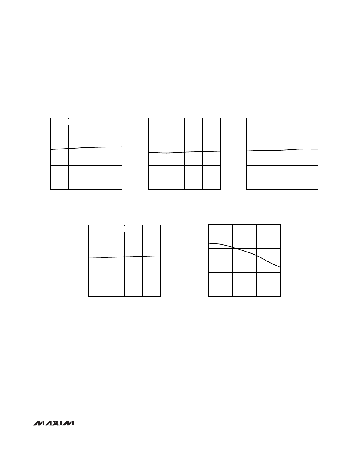
Typical Operating Characteristics (continued)
(MAX9994
Typical Application Circuit
, VCC= +5V, PLO= 0dBm, LO2 selected, PRF= -5dBm, fRF= 1400MHz to 1700MHz, LO is
High-Side Injected for a 170MHz IF, unless otherwise noted.)
CONVERSION GAIN (dB)
CONVERSION GAIN vs. FREQUENCY
10
fIF VARIES WITH f
9
8
7
1445 1465
RF
146014551450
RF FREQUENCY (MHz)
INPUT P
14
fIF FREQ VARIES WITH f
13
INPUT IP3 vs. RF FREQUENCY
27
fIF VARIES WITH f
MAX9994 toc36
vs. FREQUENCY
1dB
RF
PRF = -5dBm/TONE
26
INPUT IP3 (dBm)
25
24
1445 1465
RF
RF FREQUENCY (MHz)
MAX9994 toc39
2LO - 2RF RESPONSE vs. RF FREQUENCY
80
fIF FREQ VARIES WITH f
MAX9994 toc37
146014551450
PRF = -5dBm
70
60
2LO - 2RF RESPONSE (dBc)
50
1445 1465
LO LEAKAGE AT IF PORT
vs. LO FREQUENCY
-20
-30
RF
MAX9994 toc38
146014551450
RF FREQUENCY (MHz)
MAX9994 toc40
(dBm)
1dB
P
12
11
1445 1465
RF FREQUENCY (MHz)
146014551450
-40
LO LEAKAGE AT IF PORT (dBm)
-50
1500 1800
1600 1700
LO FREQUENCY (MHz)
Page 10

MAX9994
SiGe High-Linearity, 1400MHz to 2200MHz
Downconversion Mixer with LO Buffer/Switch
10 ______________________________________________________________________________________
Typical Operating Characteristics (continued)
(MAX9994
Typical Application Circuit
, VCC= +5V, PLO= 0dBm, LO1 selected, PRF= -5dBm, fRF= 1400MHz to 1700MHz, LO is
High-Side Injected for a 150MHz IF, unless otherwise noted.)
CONVERSION GAIN vs. FREQUENCY
10
fIF VARIES WITH f
9
8
CONVERSION GAIN (dB)
7
1429 1579
1479 1529
RF FREQUENCY (MHz)
RF
(dBm)
1dB
P
14
13
12
INPUT P
1dB
fIF VARIES WITH f
27
MAX9994 toc41
26
INPUT IP3 (dBm)
25
24
1496 1511
vs. RF FREQUENCY
RF
INPUT IP3 vs. RF FREQUENCY
fIF VARIES WITH f
PRF = -5dBm/TONE
RF
1501 1506
RF FREQUENCY (MHz)
MAX9994 toc44
LO LEAKAGE AT IF PORT (dBm)
-20
-30
-40
2LO - 2RF RESPONSE vs. RF FREQUENCY
80
fIF VARIES WITH f
MAX9994 toc42
PRF = -5dBm
70
60
2LO - 2RF RESPONSE (dBc)
50
1496 1511
LO LEAKAGE AT IF PORT
vs. LO FREQUENCY
RF
MAX9994 toc43
1501 1506
RF FREQUENCY (MHz)
MAX9994 toc45
11
1496 1511
1501 1506
RF FREQUENCY (MHz)
-50
1500 1800
1600 1700
LO FREQUENCY (MHz)
Page 11

MAX9994
SiGe High-Linearity, 1400MHz to 2200MHz
Downconversion Mixer with LO Buffer/Switch
______________________________________________________________________________________ 11
Detailed Description
The MAX9994 high-linearity downconversion mixer provides 8.3dB of conversion gain and 26.2dBm of IIP3,
with a typical 9.7dB noise figure. The integrated baluns
and matching circuitry allow for 50Ω single-ended interfaces to the RF and the two LO ports. A single-pole,
double-throw (SPDT) switch provides 50ns switching
time between the two LO inputs with 45dB of LO-to-LO
isolation. Furthermore, the integrated LO buffer provides a high drive level to the mixer core, reducing the
LO drive required at the MAX9994’s inputs to a range
of -3dBm to +3dBm. The IF port incorporates a differential output, which is ideal for providing enhanced IIP2
performance.
Specifications are guaranteed over broad frequency
ranges to allow for use in WCDMA, TD-SCDMA, LTE,
TD-LTE, cdma2000, and 2G/2.5G/3G DCS1800 and
PCS1900 base stations. The MAX9994 is specified to
operate over a 1400MHz to 2200MHz RF frequency
range, a 1400MHz to 2000MHz LO frequency range,
and a 40MHz to 350MHz IF frequency range. Operation
beyond these ranges is possible; see the
Typical
Operating Characteristics
for additional details.
With a wide LO range of 1400MHz to 2000MHz, the
MAX9994 can be used in either high-side or low-side
LO injection architectures, depending on the RF band
of interest. Higher LO applications are supported by
the MAX9996, which is pin-pin and functionally compatible with the MAX9994.
RF Input and Balun
The MAX9994 RF input is internally matched to 50Ω,
requiring no external matching components. A DCblocking capacitor is required because the input is
internally DC shorted to ground through the on-chip
balun. Input return loss is typically 21dB over the entire
1700MHz to 2200MHz RF frequency range.
LO Inputs, Buffer, and Balun
The MAX9994 can be used for either high-side or lowside injection applications with a 1400MHz to 2000MHz
LO frequency range. For a device with a 1900MHz to
2400MHz LO frequency range, refer to the MAX9996
data sheet. As an added feature, the MAX9994 includes
an internal LO SPDT switch that can be used for frequency-hopping applications. The switch selects one of
the two single-ended LO ports, allowing the external
oscillator to settle on a particular frequency before it is
Pin Description
PIN NAME FUNCTION
1, 6, 8, 14 V
2RF
3 TAP
4, 5, 10, 12,
13, 17
7 LOBIAS Bias Resistor for Internal LO Buffer. Connect a 549Ω ±1% resistor from LOBIAS to the power supply.
9 LOSEL Local Oscillator Select. Logic control input for selecting LO1 or LO2.
11 LO1 Local Oscillator Input 1. Drive LOSEL low to select LO1.
15 LO2 Local Oscillator Input 2. Drive LOSEL high to select LO2.
16 LEXT
18, 19 IF-, IF+
20 IFBIAS IF Bias Resistor Connection for IF Amplifier. Connect an 806Ω resistor from IFBIAS to GND.
— EP Exposed Pad. Solder the exposed pad to the ground plane using multiple vias.
CC
GND Ground
Power-Supply Connection. Bypass each VCC pin to GND with capacitors as shown in the Typical
Application Circuit.
Single-Ended 50Ω RF Input. This port is internally matched and DC shorted to GND through a balun.
Requires an external DC-blocking capacitor.
Center Tap of the Internal RF Balun. Bypass to GND with capacitors close to the IC, as shown in the
Typical Application Circuit.
External Inductor Connection. Connect a low-ESR, 10nH inductor from LEXT to GND. This inductor
carries approximately 100mA DC current.
Differential IF Outputs. Each output requires external bias to V
Application Circuit).
through an RF choke (see the Typical
CC
Page 12

MAX9994
SiGe High-Linearity, 1400MHz to 2200MHz
Downconversion Mixer with LO Buffer/Switch
12 ______________________________________________________________________________________
switched in. LO switching time is typically less than
50ns, which is more than adequate for virtually all GSM
applications. If frequency hopping is not employed, set
the switch to either of the LO inputs. The switch is controlled by a digital input (LOSEL): logic-high selects
LO2, logic-low selects LO1. LO1 and LO2 inputs are
internally matched to 50Ω, requiring only a 22pF DC
blocking capacitor.
A two-stage internal LO buffer allows a wide input
power range for the LO drive. All guaranteed specifications are for an LO signal power from -3dBm to +3dBm.
The on-chip low-loss balun, along with an LO buffer,
drives the double-balanced mixer. All interfacing and
matching components from the LO inputs to the IF outputs are integrated on-chip.
High-Linearity Mixer
The core of the MAX9994 is a double-balanced, highperformance passive mixer. Exceptional linearity is provided by the large LO swing from the on-chip LO
buffer. When combined with the integrated IF amplifiers, the cascaded IIP3, 2RF - 2LO rejection, and NF
performance is typically 26.2dBm, 67dBc, and 9.7dB,
respectively.
Differential IF Output Amplifier
The MAX9994 mixer has a 40MHz to 350MHz IF frequency range. The differential, open-collector IF output
ports require external pullup inductors to VCC. Note that
these differential outputs are ideal for providing
enhanced 2RF - 2LO rejection performance. Singleended IF applications require a 4:1 balun to transform
the 200Ω differential output impedance to a 50Ω singleended output. After the balun, the IF return loss is better than 15dB.
Applications Information
Input and Output Matching
The RF and LO inputs are internally matched to 50Ω.
No matching components are required. Return loss at
the RF port is typically 21dB over the 1700MHz to
2200MHz input range, and the return loss at the LO
port is typically better than 14dB (1400MHz to
2000MHz). RF and LO inputs require only DC-blocking
capacitors for interfacing.
The IF output impedance is 200Ω (differential). For
evaluation, an external low-loss 4:1 (impedance ratio)
balun transforms this impedance down to a 50Ω singleended output (see the
Typical Application Circuit
).
Bias Resistors
Bias currents for the LO buffer and the IF amplifier are
optimized by fine tuning resistors R1 and R2. If
reduced current is required at the expense of performance, contact the factory for details. If the ±1% bias
resistor values are not readily available, substitute standard ±5% values.
LEXT Inductor
Short LEXT to ground using a 0Ω resistor. For applications requiring improved RF-to-IF and LO-to-IF isolation,
a 10nH inductor (L3) can be used in place of the 0Ω
resistor. However, in order to ensure stable operation,
the mixer IF ports must be presented with a low common-mode load impedance. Contact the factory for
details. Since approximately 100mA flows through
LEXT, it is important to use a low-DCR wire-wound
inductor.
Layout Considerations
A properly designed PC board is an essential part of
any RF/microwave circuit. Keep RF signal lines as short
as possible to reduce losses, radiation, and inductance. For the best performance, route the ground pin
traces directly to the exposed pad under the package.
The PC board exposed pad MUST be connected to the
ground plane of the PC board. It is suggested that multiple vias be used to connect this pad to the lower level
ground planes. This method provides a good RF/thermal conduction path for the device. Solder the exposed
pad on the bottom of the device package to the PC
board. The MAX9994 evaluation kit can be used as a
reference for board layout. Gerber files are available
upon request at www.maxim-ic.com.
Power-Supply Bypassing
Proper voltage-supply bypassing is essential for highfrequency circuit stability. Bypass each V
CC
pin and
TAP with the capacitors shown in the
Typical
Application Circuit
; see Table 1. Place the TAP bypass
capacitor to ground within 100 mils of the TAP pin.
Exposed Pad RF/Thermal Considerations
The exposed pad (EP) of the MAX9994’s 20-pin thin
QFN-EP package provides a low thermal-resistance
path to the die. It is important that the PCB on which the
MAX9994 is mounted be designed to conduct heat
from the EP. In addition, provide the EP with a lowinductance path to electrical ground. The EP MUST be
soldered to a ground plane on the PCB, either directly
or through an array of plated via holes.
Page 13

MAX9994
SiGe High-Linearity, 1400MHz to 2200MHz
Downconversion Mixer with LO Buffer/Switch
______________________________________________________________________________________ 13
Table 1. Component List Referring to the Typical Application Circuit
Pin Configuration/Functional Diagram
MAX9994
1
2
3
4
5
15
14
13
12
11
6
7
8
9
10
20
19
18
17
16
GND
LOSEL
LOBIAS
TAP
RF
V
CC
V
CC
V
CC
V
CC
GND
GND
LO2
GND
LEXT
IFBIAS
IF-
IF+
GND
LO1
GND
+
COMPONENT VALUE DESCRIPTIO N
C1 4pF Microwa ve capacitor (0603)
C2, C6, C7, C8, C10, C12 22pF Microwave capac itors (0603)
C3, C5, C9, C11 0.01µF Microwa ve capacitors (0603)
C4 10pF Microwa ve capacitor (0603)
C13, C14 150pF Microwa ve capacitors (0603)
C15 150pF Microwa ve capacitor (0402)
L1, L2 470nH Wire-wound high-Q inductor s (0805)
L3 10nH Wire-wound high-Q inductor (0603)
R1 806 ±1% res istor (0603)
R2 549 ±1% res istor (0603)
R3 7.15 ±1% resistor (1206)
T1 4:1 balun IF balun
U1 MAX9994 Maxim IC
Page 14

MAX9994
SiGe High-Linearity, 1400MHz to 2200MHz
Downconversion Mixer with LO Buffer/Switch
14 ______________________________________________________________________________________
Typical Application Circuit
Chip Information
PROCESS: SiGe BiCMOS
Package Information
For the latest package outline information and land patterns,
go to www.maxim-ic.com/packages
. Note that a “+”, “#”, or
“-” in the package code indicates RoHS status only. Package
drawings may show a different suffix character, but the drawing
pertains to the package regardless of RoHS status.
PACKAGE
TYPE
PACKAGE
CODE
OUTLINE
NO.
LAND
PATTERN NO.
20 TQFN-EP T2055+3
21-0140 90-0008
V
CC
T1
R3
326
L1
IF
OUTPUT
C3
INPUT
C13
C14
V
CC
C2
C1
RF
C5
C4
V
TAP
GND
GND
CC
1
RF
2
3
4
5
V
CC
L2
R1
IFBIAS
20
6
CC
V
R2
C6 C7
IF+
19
7
LOBIAS
4
LEXT
GND
1
L3
16
LO2
15
V
14
GND
13
GND
12
LO1
11
10
LOSEL
INPUT
C12
CC
C10
C11
LO2
INPUT
V
CC
LO1
INPUT
C15
GND
IF-
18
17
MAX9994
8
9
CC
V
LOSEL
C8
C9
V
CC
Page 15

MAX9994
SiGe High-Linearity, 1400MHz to 2200MHz
Downconversion Mixer with LO Buffer/Switch
Maxim cannot assume responsibility for use of any circuitry other than circuitry entirely embodied in a Maxim product. No circuit patent licenses are
implied. Maxim reserves the right to change the circuitry and specifications without notice at any time.
Maxim Integrated Products, 120 San Gabriel Drive, Sunnyvale, CA 94086 408-737-7600 ____________________
15
© 2010 Maxim Integrated Products Maxim is a registered trademark of Maxim Integrated Products, Inc.
Revision History
REVISION
NUMBER
0 10/04 Initial release —
1 12/10
REVISION
DATE
DESCRIPTION
Updated Title, General Description, Ordering Information, Absolute Maximum Ratings,
Electrical Characteristics, Typical Operating Characteristics, Pin Description, General
Description, and Applications Information sections
PAGES
CHANGED
1–12
 Loading...