

Page 1
MAX9993
High-Linearity 1700MHz to 2200MHz Down-
Conversion Mixer with LO Buffer/Switch
________________________________________________________________ Maxim Integrated Products 1
19-2596; Rev 0; 10/02
For pricing, delivery, and ordering information, please contact Maxim/Dallas Direct! at
1-888-629-4642, or visit Maxim’s website at www.maxim-ic.com.
General Description
The MAX9993 high-linearity down-conversion mixer
provides 8.5dB of gain, +23.5dBm IIP3, and 9.5dB NF
for UMTS, DCS, and PCS base-station applications.
The MAX9993 integrates baluns in the RF and LO ports,
a dual-input LO selectable switch, an LO buffer, a double-balanced mixer, and a differential IF output amplifier. The MAX9993 requires a typical LO drive of +3dBm,
and supply current is guaranteed to below 230mA.
The MAX9993 is available in a compact 20-pin thin
QFN package (5mm ✕5mm) with an exposed pad.
Electrical performance is guaranteed over the extended
-40°C to +85°C temperature range.
The MAX9993 EV kit is available; contact the factory for
more information.
Applications
UMTS and 3G Base Stations
DCS1800 and EDGE Base Stations
PCS1900 Base Stations
Point-to-Point Microwave Systems
Wireless Local Loop
Private Mobile Radio
Military Systems
Features
♦ +23.5dBm Input IIP3
♦ 1700MHz to 2200MHz RF Frequency Range
♦ 40MHz to 350MHz IF Frequency Range
♦ 1400MHz to 2000MHz LO Frequency Range
♦ 8.5dB Conversion Gain
♦ 9.5dB Noise Figure
♦ Integrated LO Buffer
♦ Switch-Selectable (SPDT), Two LO Inputs
♦ Low 0 to +6dBm LO Drive
♦ 40dB LO1-to-LO2 Isolation
Ordering Information
*EP = Exposed pad.
20
19
18
17
16
13
12
11
14
15
4
3
2
1
5
6
7
8
9
10
TOP VIEW
THIN QFN
V
CC
RF
TAP
GND
V
CC
LOBIAS
LO1
GND
GND
LO2
LOSEL
LEXT
IFBIAS
IF+
IF-
GND
V
CC
GND
GND
GND
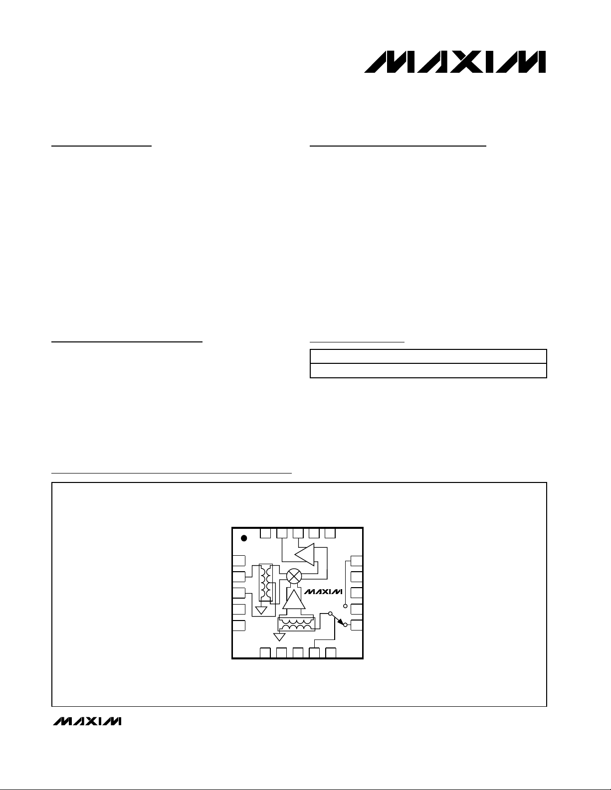
MAX9993
Pin Configuration/Functional Diagram
PART TEMP RANGE PIN-PACKAGE
MAX9993ETP-T -40°C to 85°C 20 Thin QFN-EP*
Page 2
MAX9993
High-Linearity 1700MHz to 2200MHz DownConversion Mixer with LO Buffer/Switch
2 _______________________________________________________________________________________
ABSOLUTE MAXIMUM RATINGS
Stresses beyond those listed under “Absolute Maximum Ratings” may cause permanent damage to the device. These are stress ratings only, and functional
operation of the device at these or any other conditions beyond those indicated in the operational sections of the specifications is not implied. Exposure to
absolute maximum rating conditions for extended periods may affect device reliability.
VCC..........................................................................-0.3V to 5.5V
RF (RF is DC shorted to GND through balun).....................50mA
LO1, LO2 to GND ...............................................................±0.3V
TAP, IF+, IF- to GND ..................................-0.3V to (V
CC
+ 0.3V)
LOSEL to GND ................................-0.3V to (V
CC
(pin 8) + 0.3V)
LOBIAS, IFBIAS, LEXT to GND ..................-0.3V to (V
CC
+ 0.3V)
RF and LO Input Power ..................................................+22dBm
Continuous Power Dissipation (T
A
= +70°C)
20-Lead Thin QFN
(derate 30.3mW/°C above T
A
= +70°C) ....................2200mW
θ
JA
....................................................................................33°C/W
Operating Temperature Range ...........................-40°C to +85°C
Storage Temperature Range .............................-65°C to +150°C
Lead Temperature (soldering, 10s) .................................+300°C
DC ELECTRICAL CHARACTERISTICS
(Typical Operating Circuit as shown, no input RF or LO signals applied. VCC= 4.75V to 5.25V, TA= -40°C to +85°C. Typical values are
at V
CC
= 5.0V and TA= +25°C, unless otherwise noted.)
AC ELECTRICAL CHARACTERISTICS
(Typical Operating Circuit, 4.75V < VCC< 5.75V, -40°C < TA< +85°, RF and LO ports are driven from 50Ω sources, 0dBm < PLO<
+6dBm, P
RF
= -5dBm, 1700MHz < fRF< 2200MHz, 1400MHz < fLO< 2000MHz, fIF= 200MHz. Typical values are for TA= +25°C
V
CC
= 5.0V, PLO= +3dBm, fRF= 1900MHz, fLO= 1700MHz, 200MHz IF.) (Notes 1, 2)
PARAMETER SYMBOL CONDITIONS MIN TYP MAX UNITS
Supply Voltage V
LOSEL Input High Voltage V
LOSEL Input Low Voltage V
LOSEL Input Current IIL and I
CC
CC
Total supply current 202 230
VCC (pin 8) 87 105Supply Current I
IF+/IF- (total of both) 103 133
IH
IL
IH
4.75 5.00 5.25 V
2.0 V
0.8 V
-5 +5 µA
mA
RF Frequency f
LO Frequency f
IF Frequency f
Conversion Gain G
Gain Variation Over Temperature TA = -40°C to +85°C 0.0012 dB/°C
Gain Variation from Nominal (3σ) 0.45 dB
Input Compression Point P
Input Third-Order Intercept Point
(Note 3)
PARAMETER SYMBOL CONDITIONS MIN TYP MAX UNITS
RF
LO
IF
1dB
IIP3
(Note 6) 1400 2000 MHz
(Note 3) 8.5 dB
C
Two RF tones: -5dBm each at 1950MHz
and 1951MHz, LO: +3dBm at 1750MHz
Two RF tones: -5dBm each at 2200MHz
and 2201MHz, LO: +3dBm at 2000MHz
1700 2200 MHz
50 350 MHz
12.6 dBm
24
dBm
23
Page 3
MAX9993
High-Linearity 1700MHz to 2200MHz Down-
Conversion Mixer with LO Buffer/Switch
_______________________________________________________________________________________ 3
AC ELECTRICAL CHARACTERISTICS (continued)
(Typical Operating Circuit, 4.75V < VCC< 5.75V, -40°C < TA< +85°, RF and LO ports are driven from 50Ω sources, 0dBm < PLO<
+6dBm, P
RF
= -5dBm, 1700MHz < fRF< 2200MHz, 1400MHz < fLO< 2000MHz, fIF= 200MHz. Typical values are for TA= +25°C
V
CC
= 5.0V, PLO= +3dBm, fRF= 1900MHz, fLO= 1700MHz, 200MHz IF.) (Notes 1, 2)
Note 1: Guaranteed by design and characterization.
Note 2: All limits reflect losses of external components. Output measurements taken at IFOUT of the Typical Application Circuit.
Note 3: Production tested.
Note 4: Measured at IF port at IF frequency. f
LO1
and f
LO2
are offset by 1MHz, P
LO1
= P
LO2
= +3dBm.
Note 5: IF return loss can be optimized by external matching components.
Note 6: Operation outside this range is possible, but with degraded performance of some specifications.
IIP3 Variation Over Temperature TA = -40°C to +85°C ±0.5 dB
Noise Figure NF
Required LO Drive P
Spurious Response at IF
Maximum LO-to-RF Leakage
Maximum LO-to-IF Leakage
Minimum RF-to-IF Isolation fRF = 1700MHz to 2200MHz 37 dB
Conversion Loss, LO to IF
LO Switching Time
LO1-to-LO2 Isolation (Note 4) 40 dB
RF Return Loss 19 dB
LO Return Loss
IF Return Loss RF terminated, PLO = +3dBm (Note 5) 15 dB
PARAMETER SYMBOL CONDITIONS MIN TYP MAX UNITS
f
= 1950MHz, fLO = 1750MHz,
LO
2 ✕ 2
3
✕ 3
RF
measured single-side band
0 3 6 dBm
2 RF - 2 LO
= -5dBm
P
RF
f
= 1950MHz
RF
= 1750MHz
f
LO
f
= 1850MHz
SPUR
3 RF - 3 LO
P
= -5dBm
RF
= 1950MHz
f
RF
f
= 1750MHz
LO
= 1816.66MHz
f
SPUR
P
= 0dBm to +6dBm,
LO
= 1400MHz to 2000MHz
f
LO
P
= 0dBm to +6dBm,
LO
= 1400MHz to 2000MHz
f
LO
P
= +0dBm, inject -20dBm at 200MHz
LO
into LO port, measure 200MHz at IF
50% of LOSEL to IF settled to within
2 degrees
LO port selected 15
LO port unselected 14
PLO = +3dBm 65
= +6dBm 70
P
LO
PLO = +3dBm 67
P
= +6dBm 68
LO
9.5 dB
dBc
-19 dBm
-21 dBm
28 dB
<50 ns
dB
Page 4
MAX9993
High-Linearity 1700MHz to 2200MHz DownConversion Mixer with LO Buffer/Switch
4 _______________________________________________________________________________________
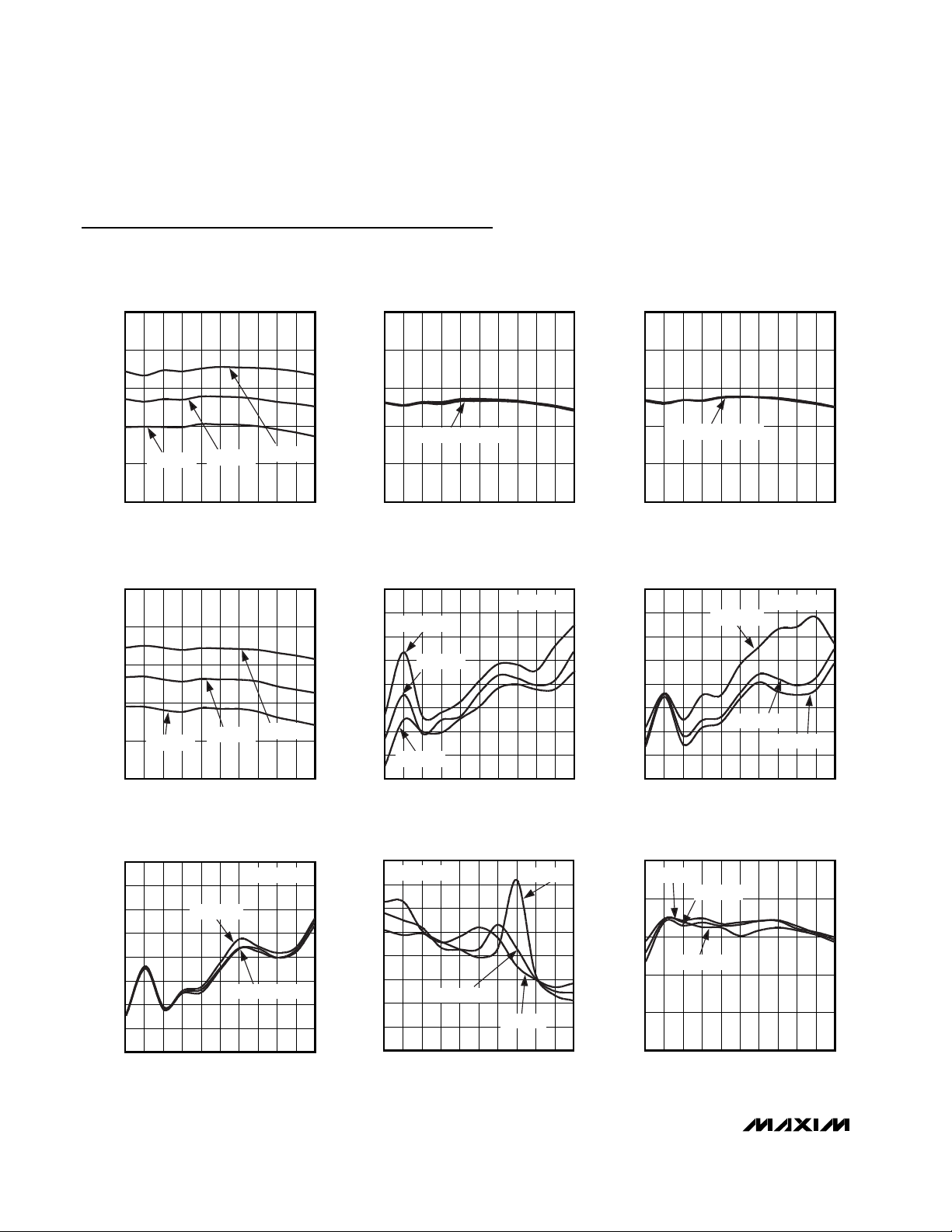
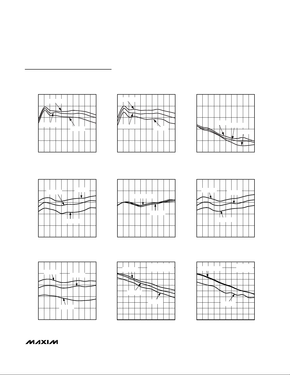
Typical Operating Characteristics
(MAX9993 EV Kit, VCC= 5.0V, PRF= -5dBm, PLO= +3dBm, LO is low-side injected for a 200MHz IF, TA= +25°C. For high-side LO
injection curves, LO frequency is beyond maximum specified range, and is shown for completeness.)
INPUT IP3 vs. RF FREQUENCY
LOW-SIDE INJECTION
MAX9993-09
RF FREQUENCY (MHz)
INPUT IP3 (dBm)
22
23
24
25
26
21
TA = +85°C
TA = +25°C
TA = -40°C
2150210020502000195019001850180017501700 2200
2 LO - 2 RF RESPONSE vs. RF FREQUENCY
HIGH-SIDE INJECTION
MAX9993-08
2 LO - 2 RF RESPONSE (dBc)
50
55
60
65
70
75
80
85
45
RF FREQUENCY (MHz)
2150210020502000195019001850180017501700 2200
TA = -40°C
TA = +25°C
TA = +85°C
PRF = -5dBm
2 RF - 2 LO RESPONSE vs. RF FREQUENCY
LOW-SIDE INJECTION
MAX9993-07
2 RF- 2 LO RESPONSE (dBc)
50
55
60
65
70
75
80
85
45
RF FREQUENCY (MHz)
2150210020502000195019001850180017501700 2200
VCC = 5.25V
VCC = 4.75V, 5.0V
PRF = -5dBm
2 RF - 2 LO RESPONSE vs. RF FREQUENCY
LOW-SIDE INJECTION
MAX9993-06
2 RF- 2 LO RESPONSE (dBc)
50
55
60
65
70
75
80
85
45
RF FREQUENCY (MHz)
2150210020502000195019001850180017501700 2200
PLO = +6dBm
PLO = +3dBm
PLO = 0dBm
PRF = -5dBm
2 RF - 2 LO RESPONSE vs. RF FREQUENCY
LOW-SIDE INJECTION
MAX9993-05
2 RF- 2 LO RESPONSE (dBc)
50
55
60
65
70
75
80
85
45
RF FREQUENCY (MHz)
2150210020502000195019001850180017501700 2200
TA = +85°C
TA = -40°C
TA = +25°C
PRF = -5dBm
CONVERSION GAIN vs. RF FREQUENCY
HIGH-SIDE INJECTION
MAX9993-04
RF FREQUENCY (MHz)
CONVERSION GAIN (dB)
7
8
9
10
11
6
TA = +85°C
TA = +25°C
TA = -40°C
2150210020502000195019001850180017501700 2200
CONVERSION GAIN vs. RF FREQUENCY
LOW-SIDE INJECTION
MAX9993-03
RF FREQUENCY (MHz)
CONVERSION GAIN (dB)
7
8
9
10
11
6
VCC = 4.75V, 5.0V, 5.25V
2150210020502000195019001850180017501700 2200
CONVERSION GAIN vs. RF FREQUENCY
LOW-SIDE INJECTION
MAX9993-02
RF FREQUENCY (MHz)
CONVERSION GAIN (dB)
7
8
9
10
11
6
PLO = 0dBm, +3dBm, +6dBm
2150210020502000195019001850180017501700 2200
CONVERSION GAIN vs. RF FREQUENCY
LOW-SIDE INJECTION
MAX9993-01
RF FREQUENCY (MHz)
CONVERSION GAIN (dB)
7
8
9
10
11
6
TA = +85°C
TA = +25°C
TA = -40°C
2150210020502000195019001850180017501700 2200
Page 5
MAX9993
High-Linearity 1700MHz to 2200MHz Down-
Conversion Mixer with LO Buffer/Switch
_______________________________________________________________________________________ 5
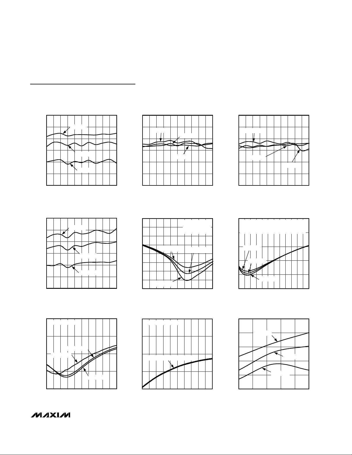
Typical Operating Characteristics (continued)
(MAX9993 EV Kit, VCC= 5.0V, PRF= -5dBm, PLO= +3dBm, LO is low-side injected for a 200MHz IF, TA= +25°C. For high-side LO
injection curves, LO frequency is beyond maximum specified range, and is shown for completeness.)
INPUT IP3 vs. RF FREQUENCY
LOW-SIDE INJECTION
26
25
24
PLO = +3dBm
23
INPUT IP3 (dBm)
22
21
PLO = +6dBm
RF FREQUENCY (MHz)
INPUT P
1dB
PLO = 0dBm
vs. RF REQUENCY
MAX9993-10
INPUT IP3 (dBm)
2150210020502000195019001850180017501700 2200
LOW-SIDE INJECTION
15
14
13
(dBm)
1dB
12
INPUT P
11
TA = +25°C
TA = +85°C
TA = -40°C
MAX9993 toc13
(dBm)
1dB
INPUT P
INPUT IP3 vs. RF FREQUENCY
LOW-SIDE INJECTION
26
VCC = 5.25V
25
24
VCC = 5.0V
23
22
21
RF FREQUENCY (MHz)
INPUT P
1dB
LOW-SIDE INJECTION
15
14
PLO = +3dBm, +6dBm
13
12
11
VCC = 4.75V
vs. RF FREQUENCY
PLO = 0dBm
2150210020502000195019001850180017501700 2200
MAX9993-11
MAX9993 toc14
INPUT IP3 (dBm)
(dBm)
1dB
INPUT P
INPUT IP3 vs. RF FREQUENCY
HIGH-SIDE INJECTION
26
25
24
TA = +85°C
23
22
21
RF FREQUENCY (MHz)
INPUT P
1dB
LOW-SIDE INJECTION
15
VCC = 5.25C
14
13
12
VCC = 4.75V
11
TA = +25°C
TA = -40°C
vs. RF FREQUENCY
V
= 5.0V
CC
2150210020502000195019001850180017501700 2200
MAX9993-12
MAX9993 toc15
10
1700 2200
RF FREQUENCY (MHz)
INPUT P
vs. RF FREQUENCY
1dB
HIGH-SIDE INJECTION
15
TA = +85°C
14
13
(dBm)
1dB
12
INPUT P
11
10
RF FREQUENCY (MHz)
TA = +25°C
TA = -40°C
215021002050200019501900185018001750
2150210020502000195019001850180017501700 2200
10
LO SWITCH ISOLATION vs. RF FREQUENCY
44
43
MAX9993 toc16
42
41
40
39
38
37
LO SWITCH ISOLATION (dB)
36
35
34
RF FREQUENCY (MHz)
LOW-SIDE INJECTION
TA = -40°C
TA = +25°C
RF FREQUENCY (MHz)
P
= P
LO1
= 1MHz
∆f
LO
TA = +85°C
LO2
2150210020502000195019001850180017501700 2200
= +3dBm
2150210020502000195019001850180017501700 2200
10
LO SWITCH ISOLATION vs. RF FREQUENCY
44
43
MAX9993 toc17
42
41
40
39
38
37
LO SWITCH ISOLATION (dB)
36
35
34
RF FREQUENCY (MHz)
LOW-SIDE INJECTION
PLO = 0dBm, +3dBm
RF FREQUENCY (MHz)
PLO = +6dBm
2150210020502000195019001850180017501700 2200
P
= P
LO1
LO2
∆fLO = 1MHz
2150210020502000195019001850180017501700 2200
MAX9993 toc18
Page 6

MAX9993
High-Linearity 1700MHz to 2200MHz DownConversion Mixer with LO Buffer/Switch
6 _______________________________________________________________________________________
Typical Operating Characteristics (continued)
(MAX9993 EV Kit, VCC= 5.0V, PRF= -5dBm, PLO= +3dBm, LO is low-side injected for a 200MHz IF, TA= +25°C. For high-side LO
injection curves, LO frequency is beyond maximum specified range, and is shown for completeness.)
LO SWITCH ISOLATION vs. RF FREQUENCY
LOW-SIDE INJECTION
44
43
42
41
40
39
38
37
LO SWITCH ISOLATION (dB)
36
35
34
VCC = 4.75, 5.00, 5.25V
RF FREQUENCY (MHz)
P
∆f
LO1
LO
= P
LO2
= 1MHz
= +3dBm
2150210020502000195019001850180017501700 2200
LO SWITCH ISOLATION vs. RF FREQUENCY
44
43
MAX9993 toc19
42
41
40
39
38
37
LO SWITCH ISOLATION (dB)
36
35
34
HIGH-SIDE INJECTION
TA = -40°C
RF FREQUENCY (MHz)
P
LO1
∆f
LO
TA = +25°C
TA = +85°C
= P
LO2
= 1MHz
= +3dBm
-30
MAX9993 toc20
-35
-40
LO LEAKAGE (dBm)
-45
-50
2150210020502000195019001850180017501700 2200
LO LEAKAGE AT IF PORT
vs. LO FREQUENCY
TA = +25°C
TA = +85°C
TA = -40°C
1400 2200
LO FREQUENCY (MHz)
MAX9993 toc21
2100200019001800170016001500
LO LEAKAGE AT IF PORT
vs. LO FREQUENCY
-30
P
= +6dBm
LO
-35
PLO = 0dBm
-40
LO LEAKAGE (dBm)
-45
PLO = +3dBm
-50
1400 2200
LO FREQUENCY (MHz)
RF-TO-IF ISOLATION vs. FREQUENCY
57.5
55.0
52.5
50.0
47.5
45.0
42.5
RF-TO-IF ISOLATION (dB)
40.0
37.5
35.0
1700 2200
TA = +85°C
TA = +25°C
RF FREQUENCY (MHz)
LO FREQUENCY (MHz)
2100200019001800170016001500
TA = -40°C
215021002000 20501800 1850 1900 19501750
213820561892 19741564 1646 1728 181014821400 2220
-30
MAX9993 toc22
-35
-40
LO LEAKAGE (dBm)
-45
-50
1400 2200
57.5
55.0
MAX9993 toc25
52.5
50.0
47.5
45.0
42.5
RF-TO-IF ISOLATION (dB)
40.0
37.5
35.0
1700 2200
LO LEAKAGE AT IF PORT
vs. LO FREQUENCY
VCC = 5.25V
VCC = 5.0V
VCC = 4.75V
2100200019001800170016001500
LO FREQUENCY (MHz)
RF-TO-IF ISOLATION vs. RF FREQUENCY
PLO = 0dBm, +3dBm, +6dBm
215021002000 20501800 1850 1900 19501750
RF FREQUENCY (MHz)
213820561892 19741564 1646 1728 181014821400 2220
LO FREQUENCY (MHz)
-15
MAX9993 toc23
-20
-25
-30
LO LEAKAGE (dBm)
-35
-40
57.5
55.0
MAX9993 toc26
52.5
50.0
47.5
45.0
42.5
RF-TO-IF ISOLATION (dB)
40.0
37.5
35.0
LO LEAKAGE AT RF PORT
vs. LO FREQUENCY
IF PORT
TERMINATED IN 50Ω
PLO = 0dBm
PLO = +3dBm
PLO = +6dBm
2300220021002000190018001700160015001400 2400
LO FREQUENCY (MHz)
RF-TO-IF ISOLATION vs. RF FREQUENCY
VCC = +4.75V, +5.0V, +5.25V
1700 2200
RF FREQUENCY (MHz)
LO FREQUENCY (MHz)
215021002000 20501800 1850 1900 19501750
213820561892 19741564 1646 1728 181014821400 2220
MAX9993 toc24
MAX9993 toc27
Page 7
MAX9993
High-Linearity 1700MHz to 2200MHz Down-
Conversion Mixer with LO Buffer/Switch
_______________________________________________________________________________________ 7
Typical Operating Characteristics (continued)
(MAX9993 EV Kit, VCC= 5.0V, PRF= -5dBm, PLO= +3dBm, LO is low-side injected for a 200MHz IF, TA= +25°C. For high-side LO
injection curves, LO frequency is beyond maximum specified range, and is shown for completeness.)
NOISE FIGURE vs. RF FREQUENCY
LOW-SIDE INJECTION
12
11
10
9
NOISE FIGURE (dB)
8
7
6
1700 2200
TA = +85°C
TA = +25°C
TA = -40°C
RF FREQUENCY (MHz)
MAX9993 toc28
215021002050200019501900185018001750
NOISE FIGURE vs. RF FREQUENCY
LOW-SIDE INJECTION
12
11
10
NOISE FIGURE (dB)
VCC = 5.25V
9
8
7
6
1700 2200
RF FREQUENCY (MHz)
VCC = 4.75V
VCC = 5.0V
MAX9993 toc29
215021002050200019501900185018001750
NOISE FIGURE vs. RF FREQUENCY
12
HIGH-SIDE INJECTION
11
10
9
NOISE FIGURE (dB)
8
7
6
1700 2200
TA = +85°C
TA = +25°C
TA = -40°C
RF FREQUENCY (MHz)
MAX9993 toc31
215021002050200019501900185018001750
RF RETURN LOSS vs. RF FREQUENCY
0
5
10
15
20
25
RF RETURN LOSS (dB)
30
35
40
1700 2200
PLO = 0dBm
PLO = +6dBm
RF FREQUENCY (MHz)
LOW-SIDE
INJECTION LO FOR
200MHz IF
PLO = +3dBm
MAX9993 toc32
215021001750 1800 1850 1950 20001900 2050
NOISE FIGURE vs. RF FREQUENCY
LOW-SIDE INJECTION
12
11
PLO = +6dBm
10
9
NOISE FIGURE (dB)
PLO = +3dBm
8
7
6
1700 2200
RF FREQUENCY (MHz)
PLO = 0dBm
IF RETURN LOSS vs. IF FREQUENCY
0
MAX9993 EV KIT
(TUNED FOR 70MHz - 100MHz IF)
SET BY EXTERNAL MATCHING COMPONENTS
5
10
VCC = 4.75V
15
IF RETURN LOSS (dB)
20
25
VCC = 5.0V
VCC = 5.25V
50 350
IF FREQUENCY (MHz)
215021002050200019501900185018001750
32530027525022520017515012510075
MAX9993 toc30
MAX9993 toc33
LO RETURN LOSS vs. LO FREQUENCY
0
LO INPUT SELECTED
5
10
LO RETURN LOSS (dB)
15
20
1400 2400
PLO = +3dBm
PLO = +6dBm
PLO = 0dBm
LO FREQUENCY (MHz)
LO RETURN LOSS vs. LO FREQUENCY
0
LO INPUT UNSELECTED
MAX9993 toc34
5
10
PLO = 0dBm, +3dBm, +6dBm
LO RETURN LOSS (dB)
15
230022002100200019001800170016001500
20
1400 2400
LO FREQUENCY (MHz)
MAX9993 toc35
230022002100200019001800170016001500
SUPPLY CURRENT vs. TEMPERATURE
205
200
195
190
SUPPLY CURRENT (mA)
185
180
-40 85
VCC = 5.25V
VCC = 5.0V
VCC = 4.75V
TEMPERATURE (°C)
MAX9993 toc36
603510-15
Page 8
MAX9993
Detailed Description
The MAX9993 high-linearity down-conversion mixer provides 8.5dB of gain and +23.5dBm IIP3, with a 9.5dB
noise figure (typ). Integrated baluns and matching circuitry allow 50Ω single-ended interfaces to the RF and
LO ports. A single-pole, double-throw (SPDT) LO switch
provides 50ns switching time between LO inputs, with
typically 40dB LO-to-LO isolation. Furthermore, the integrated LO buffer provides a high drive level to the mixer
core, reducing the LO drive required at the MAX9993’s
inputs to 0dBm to +6dBm range. The IF port incorporates a differential output, which is ideal for providing
enhanced IIP2 performance.
Specifications are guaranteed over broad frequency
ranges to allow for use in UMTS and 2G/2.5G/3G
DCS1800 and PCS1900 base stations. The MAX9993 is
specified to operate over an RF input range of
1700MHz to 2200MHz, an LO range of 1400MHz to
2000MHz, and an IF range of 40MHz to 350MHz. This
device can operate in high-side LO injection applications with an extended LO range, but performance
degrades gently as fLOcontinues to increase. See the
Typical Operating Characteristics for measurements
taken with fLOup to 2400MHz. This device is available
in a compact 5mm
✕
5mm 20-pin thin QFN package
with an exposed pad.
RF Input and Balun
The MAX9993 has one input (RF) that is internally
matched to 50Ω, requiring no external matching components. A DC-blocking capacitor is required, because
the input is internally DC shorted to ground through the
on-chip balun. Input return loss is better than 15dB over
the entire RF frequency range of 1700MHz to 2200MHz.
LO Input, Switch, Buffer, and Balun
The mixer can be used for either high-side or low-side
injection applications with an LO frequency range of
1400MHz to 2000MHz. An internal LO SPDT switch
selects one of two single-ended LO ports. This allows
the external oscillator to settle on a particular frequency
before it is switched in. LO switching time is guaranteed to be less than 50ns. This switch is controlled by a
digital input (LOSEL): logic low selects LO1, logic high
selects LO2. LO1 and LO2 inputs are internally
matched to 50Ω, requiring only a 22pF DC-blocking
capacitor.
A two-stage internal LO buffer allows a wide input power
range for the LO drive. All guaranteed specifications are
for an LO signal power from 0dBm to +6dBm. A low-loss
balun along with an LO buffer drives the double-balanced
mixer. All interfacing and matching from the LO inputs to
the IF outputs are integrated on-chip.
High-Linearity 1700MHz to 2200MHz DownConversion Mixer with LO Buffer/Switch
8 _______________________________________________________________________________________
Pin Description
PIN NAME FUNCTION
1, 6, 8 V
2RF
3 TAP
4, 5, 10, 12,
13, 14, 17, EP
7 LOBIAS LO Output Bias Resistor for LO Buffer. Connect a 383Ω (±1%) from LOBIAS to GND.
9 LOSEL LO Select. Logic control input for selecting LO1 or LO2.
11 LO1 Local Oscillator Input. LO1 selected when LOSEL is low.
15 LO2 Local Oscillator Input. LO2 selected when LOSEL is high.
16 LEXT
18 IF-
19 IF+
20 IFBIAS IF Bias Resistor Connection for IF Amplifier. Connect a 523Ω (±1%) from IFBIAS to GND.
CC
GND
Power Supply Connections. See the Typical Application Circuit.
Single-Ended 50Ω RF Input. This port is internally matched and DC shorted to GND through a
balun. Provide a DC-blocking capacitor if required.
Center Tap of the Internal RF Balun. Bypass with capacitors close to the IC, as shown in the
Typical Application Circuit.
Ground. Connect to supply ground. Provide multiple vias in the PC board to create a lowinductance connection between the exposed paddle (EP) and the PC board ground.
External Inductor Connection. Connect a low-ESR 10nH inductor from LEXT to GND. This inductor
carries approximately 100mA DC current.
Noninverting IF Output. Requires external bias to V
Application Circuit).
Inverting IF Output. Requires external bias to V
Application Circuit).
through an RF choke (see the Typical
CC
through an RF choke (see the Typical
CC
Page 9

High-Linearity Mixer
The core of the MAX9993 is a double-balanced, highperformance passive mixer. Exceptional linearity is provided by the large LO swing from the on-chip LO
buffer; IIP3 is typically +23.5dBm, IIP2 is typically
+60dBm, and total cascaded NF is 9.5dB.
Differential IF Output Amplifier
The MAX9993 mixer has an IF frequency range of 40MHz
to 350MHz. The differential, open-collector IF output ports
require external pullup inductors to VCC. Single-ended IF
applications require a 4:1 balun to transform the 200Ω
differential output impedance to a 50Ω single-ended output. After the balun, VSWR is typically 1.5:1.
Applications Information
Input and Output Matching
The RF and LO inputs are internally matched to 50Ω.
No matching components are required. Return loss at
the RF port is better than 15dB over the entire input
range, 1700MHz to 2200MHz, and return loss at LO1
and LO2 is better than 10dB from 1400MHz to
2000MHz. RF and LO inputs require only DC-blocking
capacitors for interfacing. These DC-blocking capacitors can be part of the matching circuit.
The IF output impedance is 200Ω differential out of the
IC. An external low-loss 4:1 balun brings this impedance down to a 50Ω single-ended output (see the
Typical Application Circuit).
Bias Resistors
Bias currents for the LO buffer and the IF amplifier were
optimized by fine-tuning the resistors at LOBIAS and
IFBIAS during characterization at the factory. These currents should not be adjusted. If the 383Ω (±1%) and/or
523Ω (±1%) resistor values are not readily available,
substitute standard ±5% values: 390Ω and 520Ω ,
respectively.
Layout Considerations
A properly designed PC board is an essential part of
any RF/microwave circuit. Keep RF signal lines as short
as possible to reduce losses, radiation, and inductance. For best performance, route the ground pin
traces directly to the exposed pad underneath the
package. This pad should be connected to the ground
plane of the board by using multiple vias under the
device to provide the best RF/thermal conduction path.
Solder the exposed pad on the bottom of the device
package to a PC board exposed pad.
Power Supply Bypassing
Proper voltage supply bypassing is essential for highfrequency circuit stability. Bypass each VCCpin and
TAP with the capacitors shown in the typical application
circuit. Place the TAP bypass capacitor to ground within 100 mils of the TAP pin.
Chip Information
TRANSISTOR COUNT: 989
PROCESS: SiGe BiCMOS
MAX9993
High-Linearity 1700MHz to 2200MHz Down-
Conversion Mixer with LO Buffer/Switch
_______________________________________________________________________________________ 9
Table 1. Component List
COMPONENT VALUE SIZE DESCRIPTION
C1 4pF 0603 Microwave capacitor
C2, C6, C7, C9, C10 22pF 0603 Microwave capacitors
C3, C5, C8 0.01µF 0603 Capacitors
C4 10pF 0603 Microwave capacitor
C11, C12, C13 150pF 0603 Microwave capacitors
L1, L2 470nH 1008 Wire-wound high-Q inductors
L3 10nH 0805 Wire-wound high-Q inductor
R1 523Ω 0603 ±1% resistor
R2 383Ω 0603 ±1% resistor
R3, R4 7.2Ω 1206 ±1% resistors
R5 200Ω 0603 ±5% resistor
T1 4:1 (200:50) — IF balun
Page 10

MAX9993
High-Linearity 1700MHz to 2200MHz DownConversion Mixer with LO Buffer/Switch
10 ______________________________________________________________________________________
Typical Application Circuit
C12
5.0V
2
1
T1
63
4:1 (200:50)
TRANSFORMER
4
IF OUT
R4
C11
R1
L1
L2
C13
5.0V
R3
5.0V
C3
RFIN
R5
C5
C2
V
CC
TAP
GND
GND
1
RF
2
3
4
5
C1
C4
5.0V
R2
C6
IF+
GND
IF-
IFBIAS
20
19
18
17
MAX9993
6
7
8
9
CC
CC
V
V
LOSEL
LOBIAS
C8
C7
LEXT
GND
L3
16
LO2
15
GND
14
GND
13
GND
12
LO1
11
10
C10
L02
L01
C9
LO SELECT
Page 11
MAX9993
High-Linearity 1700MHz to 2200MHz Down-
Conversion Mixer with LO Buffer/Switch
______________________________________________________________________________________ 11
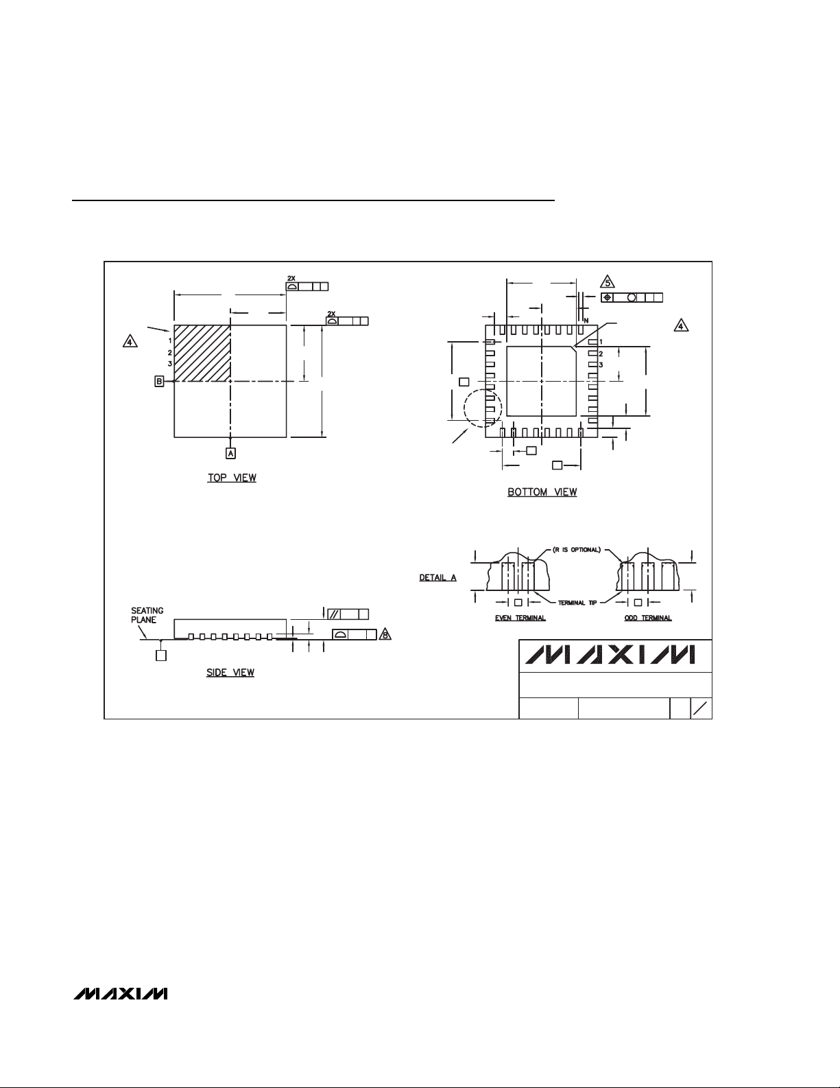
Package Information
(The package drawing(s) in this data sheet may not reflect the most current specifications. For the latest package outline information,
go to www.maxim-ic.com/packages.)
QFN THIN.EPS
D2
(ND-1) X e
e
D
C
PIN # 1
I.D.
(NE-1) X e
E/2
E
0.08 C
0.10
C
A
A1
A3
DETAIL A
0.15
C B
0.15 C A
DOCUMENT CONTROL NO.
21-0140
PACKAGE OUTLINE
16, 20, 28, 32L, QFN THIN, 5x5x0.8 mm
PROPRIETARY INFORMATION
APPROVAL
TITLE:
C
REV.
2
1
E2/2
E2
0.10 M
C A B
PIN # 1 I.D.
b
0.35x45
L
D/2
D2/2
L
C
L
C
e e
L
CC
L
k
k
L
L
Page 12

MAX9993
High-Linearity 1700MHz to 2200MHz DownConversion Mixer with LO Buffer/Switch
Maxim cannot assume responsibility for use of any circuitry other than circuitry entirely embodied in a Maxim product. No circuit patent licenses are
implied. Maxim reserves the right to change the circuitry and specifications without notice at any time.
12 ____________________Maxim Integrated Products, 120 San Gabriel Drive, Sunnyvale, CA 94086 408-737-7600
© 2002 Maxim Integrated Products Printed USA is a registered trademark of Maxim Integrated Products.
Package Information (continued)
(The package drawing(s) in this data sheet may not reflect the most current specifications. For the latest package outline information,
go to www.maxim-ic.com/packages.)
2
2
21-0140
REV.DOCUMENT CONTROL NO.APPROVAL
PROPRIETARY INFORMATION
TITLE:
COMMON DIMENSIONS
EXPOSED PAD VARIATIONS
1. DIMENSIONING & TOLERANCING CONFORM TO ASME Y14.5M-1994.
2. ALL DIMENSIONS ARE IN MILLIMETERS. ANGLES ARE IN DEGREES.
3. N IS THE TOTAL NUMBER OF TERMINALS.
4. THE TERMINAL #1 IDENTIFIER AND TERMINAL NUMBERING CONVENTION SHALL CONFORM TO JESD 95-1
SPP-012. DETAILS OF TERMINAL #1 IDENTIFIER ARE OPTIONAL, BUT MUST BE LOCATED WITHIN THE
ZONE INDICATED. THE TERMINAL #1 IDENTIFIER MAY BE EITHER A MOLD OR MARKED FEATURE.
5. DIMENSION b APPLIES TO METALLIZED TERMINAL AND IS MEASURED BETWEEN 0.25 mm AND 0.30 mm
FROM TERMINAL TIP.
6. ND AND NE REFER TO THE NUMBER OF TERMINALS ON EACH D AND E SIDE RESPECTIVELY.
7. DEPOPULATION IS POSSIBLE IN A SYMMETRICAL FASHION.
8. COPLANARITY APPLIES TO THE EXPOSED HEAT SINK SLUG AS WELL AS THE TERMINALS.
9. DRAWING CONFORMS TO JEDEC MO220.
NOTES:
10. WARPAGE SHALL NOT EXCEED 0.10 mm.
C
PACKAGE OUTLINE
16, 20, 28, 32L, QFN THIN, 5x5x0.8 mm
 Loading...