

General Description
The MAX9989 and MAX9990 LO buffers provide the high
output (+14dBm to +20dBm) necessary to drive the LO
inputs of high-linearity passive mixers, while offering 40dB
reverse isolation to prevent LO pulling. The MAX9989 is
internally matched for the cellular/GSM bands, and the
MAX9990 is matched for the DCS/PCS/UMTS bands.
The Typical Application Circuit provides a nominal
+17dBm output power with ±1dB variation over supply,
temperature, and input power. With two optional resistors, the output power can be precision set from
+14dBm to +20dBm. The devices offer more than 35dB
main driver output to PLL amp output isolation. Each
device is offered in a 5mm ✕5mm 20-pin thin QFN
package with exposed paddle.
Applications
Cellular/GSM/DCS/PCS/UMTS Base Station
Tx/Rx LO Drives
Coherent Receivers
ISM Wireless LAN
Wireless Local Loop
Local Multipoint Distribution Service
Point-to-Point Systems
Features
♦ ±1dB Output Power Variation
♦ +14dBm to +20dBm Adjustable Output Power
♦ 40dB Reverse Isolation
♦ Better Than 35dB Main Driver Output to PLL Amp
Output Isolation
♦ Low Output Noise: -170dBc/Hz at +17dBm
♦ 110mA Supply Current at +17dBm
♦ ESD Protection
♦ Isolated PLL Output (+3dBm)
MAX9989/MAX9990
+14dBm to +20dBm LO Buffers
with ±1dB Variation
________________________________________________________________ Maxim Integrated Products 1
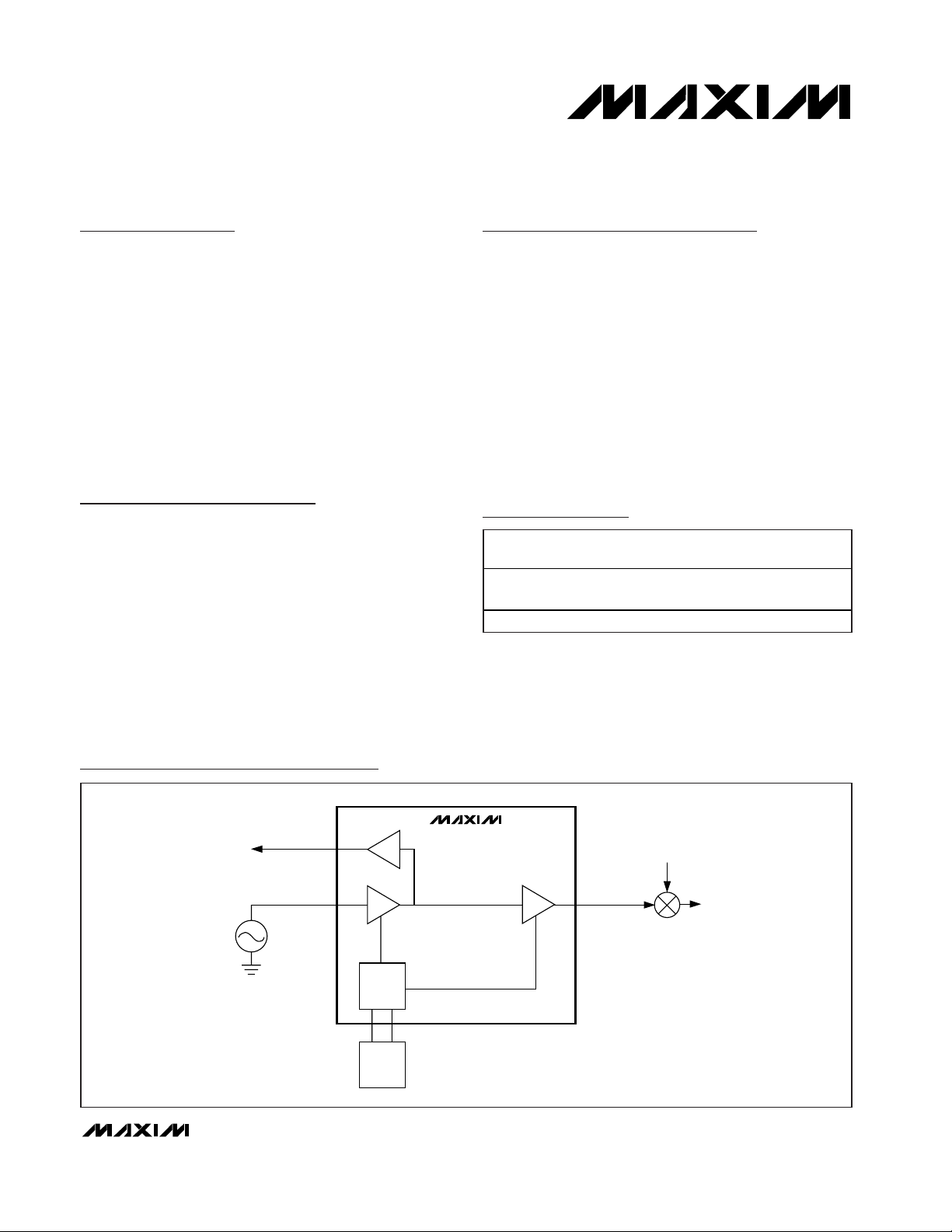
MAX9989
MAX9990
BIAS
BIASIN
RF LO
TO PLL
PRESCALER
PLL BUFFER
INPUT AMP
OUTPUT AMP
RF INPUT
IF OUTPUT
IN
(+7dBm)
OUTPLL
(+3dBm)
OUTLO
(+17dBm)
BIASOUT
BIAS
CONTROL
NETWORK
Typical Operating Circuit and Block Diagram
Ordering Information
19-2486; Rev 0; 7/02
For pricing, delivery, and ordering information, please contact Maxim/Dallas Direct! at
1-888-629-4642, or visit Maxim’s website at www.maxim-ic.com.
PART
TEMP
RANGE
PIN-
FREQUENCY
RANGE (MHz)
20 Thin
QFN-EP*
700 to 1100
1500 to 2200
*EP = Exposed paddle.
Typical Application Circuit/Pin Configuration appears at end of data sheet.
PACKAGE
MAX9989ETP -40°C to +85°C
MAX9990ETP -40°C to +85°C 20 QFN-EP*
MAX9989/MAX9990
+14dBm to +20dBm LO Buffers
with ±1dB Variation
2 _______________________________________________________________________________________
ABSOLUTE MAXIMUM RATINGS
Stresses beyond those listed under “Absolute Maximum Ratings” may cause permanent damage to the device. These are stress ratings only, and functional
operation of the device at these or any other conditions beyond those indicated in the operational sections of the specifications is not implied. Exposure to
absolute maximum rating conditions for extended periods may affect device reliability.
VCC1, VCC2, VCC3, VCCREF to GND .................-0.3V to +6.0V
IN to GND...................................................-0.3V to (V
CC
+ 0.3V)
OUTLO, OUTPLL to GND...........................-0.3V to (V
CC
+ 0.3V)
REF to GND ......................................................Source/Sink 5mA
INBIAS, OUTBIAS to GND...................................-0.3V to +0.75V
PLLBIAS ......................................................................Sink 25mA
RF Input Power ...............................................................+20dBm
Continuous Power Dissipation (T
A
= +70°C)
20-Pin Thin QFN (derate 21mW/°C above +70°C) ....1667mW
θ
JA
.................................................................................+48°C/W
Junction Temperature......................................................+150°C
Operating Temperature Range ...........................-40°C to +85°C
Storage Temperature Range .............................-65°C to +150°C
Lead Temperature (soldering, 10s) .................................+300°C
DC ELECTRICAL CHARACTERISTICS—MAX9989
(Typical Application Circuit, VCC= 4.75V to 5.25V, input and outputs terminated in 50Ω, TA= -40°C to +85°C. Typical specifications
are for V
CC
= 5.0V and TA= +25°C.) (Note 1)
PARAMETER
CONDITIONS
UNITS
Supply Voltage V
CC
V
Low power setting
(see Table 1 for resistor values)
77
Nominal power setting
(R2–R5 not installed) (Note 2)
94
116Supply Current I
CC
High power setting
(see Table 1 for resistor values)
mA
DC ELECTRICAL CHARACTERISTICS—MAX9990
(Typical Application Circuit, VCC= 4.75V to 5.25V, input and outputs terminated in 50Ω, TA= -40°C to +85°C. Typical specifications
are for V
CC
= 5.0V and TA= +25°C.) (Note 1)
PARAMETER
CONDITIONS
UNITS
Supply Voltage V
CC
V
Low power setting
(see Table 1 for resistor values)
87
Nominal power setting
(R2–R5 not installed) (Note 2)
98
122Supply Current I
CC
High power setting
(see Table 1 for resistor values)
mA
SYMBOL
MIN TYP MAX
4.75 5.00 5.25
SYMBOL
105
146
MIN TYP MAX
4.75 5.00 5.25
111
154
MAX9989/MAX9990
+14dBm to +20dBm LO Buffers
with ±1dB Variation
_______________________________________________________________________________________ 3
AC ELECTRICAL CHARACTERISTICS—MAX9989
(Typical Application Circuit, VCC= 4.75V to 5.25V, 50Ω environment, +4dBm < PIN< +10dBm, 700MHz < fIN< 1100MHz,
T
A
= -40°C to +85°C, unless otherwise noted. Typical specifications are for VCC= 5.0V, PIN= +7dBm, fIN= 900MHz, and
T
A
= +25°C, unless otherwise noted.) (Note 1)
PARAMETER
SYMBOL
CONDITIONS
MIN
TYP
MAX
UNITS
Operating Frequency f
MHz
Low power setting, PIN = +4dBm
(see Table 1 for resistor values)
Nominal power setting,
+4dBm < P
IN
< +10dBm
4.75V < V
CC
< 5.25V
-40°C < T
A
< +85°C (R2–R5 not installed)
17.3
Output Power P
OUTLO
High power setting, PIN = +10dBm
(see Table 1 for resistor values)
dBm
Output Power (PLL Driver)
3.7
dBm
Input VSWR VSWR
IN
Output VSWR
Output-Noise Power Density P
NOISE
V
CC
= 5.0V, ±100MHz offset
(R2–R5 not installed)
dBm/Hz
OUTLO to RFIN Isolation S12
V
CC
= 5.0V, nominal power setting
(R2–R5 not installed)
48 dB
AC ELECTRICAL CHARACTERISTICS—MAX9990
(Typical Application Circuit, VCC= 4.75V to 5.25V, 50Ω environment, +6dBm < PIN< +12dBm, 1500MHz < fIN< 2200MHz, and
T
A
= -40°C to +85°C, unless otherwise noted. Typical specifications are for VCC= 5.0V, PIN= +9dBm, fIN= 1800MHz, and
T
A
= +25°C, unless otherwise noted.) (Note 1)
Note 1: Devices are 100% DC screened and AC production tested for functionality. Data sheet typical specifications are derived
from the average of 30 units from a typical lot, and are tested under the conditions specified for the typical specifications.
Note 2: DC current limits at -40°C are guaranteed by design and characterization.
700 1100
14.3
±0.8
19.7
P
OUTPLL
1.2:1
VSWR
OUT
1.7:1
-152
Operating Frequency f 1500 2200 MHz
Output Power P
Output Power (PLL Driver) P
Input VSWR VSWR
Output VSWR VSWR
Output-Noise Power Density P
OUTLO to RFIN Isolation S12
PARAMETER SYMBOL CONDITIONS MIN TYP MAX UNITS
Low power setting, PIN = +6dBm
(see Table 1 for resistor values)
Nominal power setting,
OUTLO
OUTPLL
NOISEVCC
+6dBm < P
4.75V < V
-40°C < T
High power setting, PIN = +12dBm
(see Table 1 for resistor values)
IN
OUT
= 5.0V, ±100MHz offset -152 dBm/Hz
= 5.0V, nominal power setting
V
CC
(R2–R5 not installed)
< +12dBm
IN
< 5.25V
CC
< +85°C (R2–R5 not installed)
A
14.2
17.3
±0.8
19.5
3.6 dBm
1.5:1
1.4:1
49 dB
dBm
MAX9989/MAX9990
+14dBm to +20dBm LO Buffers
with ±1dB Variation
4 _______________________________________________________________________________________
MAX9989 toc01
OUTPUT POWER (dBm)
SUPPLY CURRENT (mA)
191817161514131211
105
110
115
120
100
10 20
TA = +85°C
TA = +25°C
TA = -40°C
SUPPLY CURRENT vs. OUTPUT POWER
OUTLO
20
19
18
17
16
15
14
13
12
11
10
-5 -3 -2-4 0-1 21345678910
MAX9989 toc02
INPUT POWER (dBm)
OUTPUT POWER (dBm)
OUTPUT POWER vs. INPUT POWER
OUTLO
TA = +85°C
TA = +25°C
TA = -40°C
MAX9989 toc03
INPUT POWER (dBm)
OUTPUT POWER (dBm)
862 4-2 0-4
-3
-2
-1
0
1
2
3
4
5
6
-4
-6 10
OUTPUT POWER vs. INPUT POWER
OUTPLL
TA = +85°C
TA = +25°C
TA = -40°C
MAX9989 toc04
OPERATING FREQUENCY (MHz)
OUTPUT POWER (dBm)
11001000900800700600
15
16
17
18
19
20
14
500 1200
OUTPUT POWER vs. FREQUENCY
OUTLO
TA = +85°C
TA = +25°C
TA = -40°C
MAX9989 toc05
OPERATING FREQUENCY (MHz)
OUTPUT POWER (dBm)
11001000900800700600
1
2
3
4
5
6
7
0
500 1200
OUTPUT POWER vs. FREQUENCY
OUTPLL
TA = -40°C
TA = +25°C
TA = +85°C
AMBIENT TEMPERATURE (°C)
OUTPUT POWER (dBm)
806020 400-20
16.2
16.4
16.6
16.8
17.0
17.2
17.4
17.6
17.8
18.0
16.0
107.5
108.0
108.5
109.0
109.5
110.0
110.5
111.0
111.5
112.0
107.0
-40
OUTPUT POWER AND SUPPLY CURRENT
vs. TEMPERATURE
MAX9989 toc06
SUPPLY CURRENT (mA)
P
OUTLO
I
CC
OUTPUT POWER vs. SUPPLY VOLTAGE
SUPPLY VOLTAGE (V)
OUTLO OUTPUT POWER (dBm)
5.34.7 5.14.9
14.5
15.0
15.5
16.0
16.5
17.0
17.5
18.0
14.0
4.5 5.5
MAX9989 toc07
6.0
5.0
4.5
4.0
3.5
3.0
2.5
2.0
5.5
OUTPLL OUTPUT POWER (dBm)
OUTLO
OUTPLL
Typical Operating Characteristics
(VCC= 5.0V, nominal bias, fIN= 900MHz, PIN= +7dBm, TA= +25°C, unless otherwise noted.) (Shaded regions are outside the
guaranteed operating range, and are provided for reference only.)
MAX9989

MAX9989/MAX9990
+14dBm to +20dBm LO Buffers
with ±1dB Variation
_______________________________________________________________________________________ 5
MAX9989 toc08
SUPPLY VOLTAGE (V)
SUPPLY CURRENT (mA)
5.35.14.94.7
95
100
105
110
115
120
90
4.5 5.5
SUPPLY CURRENT vs. SUPPLY VOLTAGE
PLL BIASED
PLL NOT BIASED
SMALL-SIGNAL GAIN vs. FREQUENCY
MAX9989 toc09
FREQUENCY (MHz)
GAIN (dB)
11001000900800700600
14
15
16
17
18
19
13
500 1200
VCC = 5V
T
A
= +25°C
P
IN
= -15dBm
NOMINAL BIAS
INPUT RETURN LOSS vs. FREQUENCY
MAX9989 toc10
FREQUENCY (MHz)
RETURN LOSS (dB)
1000900600 700 800
-35
-30
-25
-20
-15
-10
-5
0
-40
500 1100
VCC = 5V
T
A
= +25°C
P
IN
= +7dBm
Typical Operating Characteristics (continued)
(VCC= 5.0V, nominal bias, fIN= 900MHz, PIN= +7dBm, TA= +25°C, unless otherwise noted.) (Shaded regions are outside the
guaranteed operating range, and are provided for reference only.)
OUTPUT RETURN LOSS vs. FREQUENCY
MAX9989 toc11
FREQUENCY (MHz)
RETURN LOSS (dB)
1000900800700600
18
16
14
12
10
8
6
4
2
0
20
500 1100
VCC = 5V
T
A
= +25°C
P
IN
= +7dBm
OUTLO
OUTPLL
OUT-TO-IN ISOLATION vs. FREQUENCY
MAX9989 toc12
FREQUENCY (MHz)
ISOLATION (dB)
1000900800700600
-65
-60
-55
-50
-45
-40
-35
-30
-25
-20
-70
500 1100
VCC = 5V
T
A
= +25°C
P
IN
= +7dBm
OUTPLL TO IN
OUTLO TO IN
PLL ISOLATION vs. FREQUENCY
MAX9989 toc13
FREQUENCY (MHz)
ISOLATION (dB)
1000900800700600
-65
-60
-55
-50
-45
-40
-35
-30
-25
-20
-70
500 1100
VCC = 5V
T
A
= +25°C
P
IN
= +7dBm
OUTPLL TO
OUTLO
OUTLO TO OUTPLL
OUTPUT NOISE POWER vs. INPUT POWER
MAX9989 toc14
INPUT POWER (dBm)
NOISE POWER (dBm/Hz)
12111098765
-155
-150
-145
-140
-160
413
±100MHz OFFSET
MAX9989

MAX9989/MAX9990
+14dBm to +20dBm LO Buffers
with ±1dB Variation
6 _______________________________________________________________________________________
MAX9990 toc01
OUTPUT POWER (dBm)
SUPPLY CURRENT (mA)
161591011 1312 14
105
110
115
120
125
130
135
140
100
81817
SUPPLY CURRENT vs. OUTPUT POWER
OUTLO
TA = +85°C
TA = +25°C
TA = -40°C
20
19
18
17
16
15
14
13
12
11
10
-5 -3 -2-4 0-1 21345678910
MAX9990 toc02
INPUT POWER (dBm)
OUTPUT POWER (dBm)
OUTPUT POWER vs. INPUT POWER
OUTLO
TA = +85°C
TA = +25°C
TA = -40°C
MAX9990 toc03
INPUT POWER (dBm)
OUTPUT POWER (dBm)
862 4-2 0-4
-3
-2
-1
0
1
2
3
4
5
6
-4
-6 10
OUTPUT POWER vs. INPUT POWER
OUTPLL
TA = +85°C
TA = -40°C
TA = +25°C
MAX9990 toc04
OPERATING FREQUENCY (MHz)
OUTPUT POWER (dBm)
210020001800 190017001600
11
12
13
14
15
16
17
18
19
20
10
1500 2200
OUTPUT POWER vs. FREQUENCY
OUTLO
TA = +85°C
TA = +25°C
TA = -40°C
MAX9990 toc05
OPERATING FREQUENCY (MHz)
OUTPUT POWER (dBm)
210020001900180017001600
1
2
3
4
5
6
0
1500 2200
OUTPUT POWER vs. FREQUENCY
OUTPLL
TA = -40°C
TA = +25°C
TA = +85°C
15.0
15.5
16.0
16.5
17.0
17.5
18.0
100
105
110
115
120
125
130
AMBIENT TEMPERATURE (°C)
OUTPUT POWER (dBm)
-40 0 20-20 40 8060
OUTPUT POWER AND SUPPLY CURRENT
vs. TEMPERATURE
MAX9990 toc06
SUPPLY CURRENT (mA)
I
CC
P
OUTLO
OUTPUT POWER vs. SUPPLY VOLTAGE
SUPPLY VOLTAGE (V)
OUTLO OUTPUT POWER (dBm)
5.34.7 5.14.9
14.5
15.0
15.5
16.0
16.5
17.0
17.5
18.0
14.0
4.5 5.5
MAX9990 toc07
6.0
5.0
4.5
4.0
3.5
3.0
2.5
2.0
5.5
OUTPLL OUTPUT POWER (dBm)
OUTLO
OUTPLL
Typical Operating Characteristics (continued)
(VCC= 5.0V, nominal bias, fIN= 1800MHz, PIN= +9dBm, TA= +25°C, unless otherwise noted.) (Shaded regions are outside the
guaranteed operating range, and are provided for reference only.)
MAX9990

MAX9989/MAX9990
+14dBm to +20dBm LO Buffers
with ±1dB Variation
_______________________________________________________________________________________ 7
Typical Operating Characteristics (continued)
(VCC= 5.0V, nominal bias, fIN= 1800MHz, PIN= +9dBm, TA= +25°C, unless otherwise noted.) (Shaded regions are outside the
guaranteed operating range, and are provided for reference only.)
SUPPLY CURRENT vs. SUPPLY VOLTAGE
MAX9990 toc08
SUPPLY VOLTAGE (V)
SUPPLY CURRENT (mA)
5.35.14.94.7
105
110
115
120
100
4.5 5.5
PLL BIASED
PLL NOT BIASED
MAX9990 toc09
FREQUENCY (MHz)
GAIN (dB)
210020001600 1700 1800 1900
11
12
13
14
15
16
17
18
10
1500 2200
VCC = 5V
P
IN
= -15dBm
NOMINAL BIAS
SMALL-SIGNAL GAIN vs. FREQUENCY
OUTLO
-40°C
+25°C
+85°C
INPUT RETURN LOSS vs. FREQUENCY
MAX9990 toc10
FREQUENCY (MHz)
RETURN LOSS (dB)
210020001900180017001600
-18
-16
-14
-12
-10
-8
-6
-20
1500 2200
VCC = 5V
T
A
= +25°C
P
IN
= +9dBm
MAX9990 toc11
FREQUENCY (MHz)
RETURN LOSS (dB)
210020001600 1700 1800 1900
35
30
25
20
15
10
5
0
40
1500 2200
VCC = 5V
T
A
= +25°C
P
IN
= +9dBm
OUTPUT RETURN LOSS vs. FREQUENCY
OUTLO
OUTPLL
OUT-TO-IN ISOLATION vs. FREQUENCY
MAX9990 toc12
FREQUENCY (GHz)
ISOLATION (dB)
210020001800 190017001600
60
55
50
45
40
35
30
25
20
15
65
1500 2200
OUTPLL TO IN
OUTLO TO IN
VCC = 5V
T
A
= +25°C
P
IN
= +9dBm
PLL ISOLATION vs. FREQUENCY
MAX9990 toc13
FREQUENCY (MHz)
ISOLATION (dB)
210020001800 190017001600
-60
-55
-50
-45
-40
-35
-30
-25
-20
-15
-65
1500 2200
VCC = 5V
T
A
= +25°C
P
IN
= +9dBm
PLL TO OUTLO
OUTLO TO PLL
OUTPUT NOISE POWER vs. INPUT POWER
MAX9990 toc14
INPUT POWER (dBm)
NOISE POWER (dBm/Hz)
12111098765
-155
-150
-145
-140
-160
413
±100MHz OFFSET
MAX9990

MAX9989/MAX9990
+14dBm to +20dBm LO Buffers
with ±1dB Variation
8 _______________________________________________________________________________________
Detailed Description
The MAX9989/MAX9990 LO buffers each consist of a
single-input amplifier, an output amplifier, and a second
buffer amplifier to drive the LO’s PLL. The bias currents
for the amplifiers are adjustable through off-chip resistors, allowing the output level to be precision set anywhere from +14dBm to +20dBm. The PLL output is
preset to +3dBm (about 900mV
P-P
into 50Ω).
Power levels are typically ±1dB over the full supply, input
power, and temperature range. Precision power control
is achieved by internal control circuitry. Maintaining tight
power control keeps the system engineer from over
specifying the LO drive in order to guarantee a linearity
specification in the base-station mixer. More than 40dB
isolation between the LO output and the input prevents
VCO pulling.
The MAX9989 is specified from 700MHz to 1100MHz,
and the MAX9990 is specified from 1500MHz to
2200MHz. Both are offered in compact 5mm
✕
5mm 20-
pin QFN thin packages with EP.
Input Amplifier
A single low-noise input amplifier provides gain and isolation. The compressed output power for this stage is
controlled by the bias setting resistors R2 or R4 (see the
Typical Application Circuit). These resistors are not
required for the nominal +17dBm output; see Table 1 for
bias resistor values to obtain +14dBm to +20dBm output power.
The input is internally matched to 50Ω, and typical
VSWR is no more than 2:1 over all operating conditions.
Since the input is internally biased, provide a DC block
at the input pin.
PLL Amplifier and Output
A small amount of power is tapped off from the input
amplifier’s output, and fed to a high-isolation buffer to
drive the PLL output at about +3dBm. If the PLL output
is not required, it can be disabled by removing R1; disabling the PLL output saves 12mA supply current.
Pin Description
PIN NAME FUNCTION
1, 4, 8, 9,
13–18, EP
GND
Ground. Provide 5–10 plated vias from EP to system ground plane for optimal thermal and RF
performance.
2 IN Input. Internally matched 50Ω RF input. AC couple to this pin so as not to disturb input bias level.
3
Supply. Supply connection for on-chip voltage and current references. See Applications Information
for information on decoupling.
5 REF
Voltage Reference Output. Output for on-chip 1.5V bandgap voltage reference. See the
Applications Information section for information on decoupling.
6 BIASIN
Bias Connection for Input Buffer. Set compressed power point for input amplifier with a resistor to
REF or GND. For +17dBm output power, no external biasing resistors are required. See the
Applications Information section for more information.
7
Bias Connection for LO Output Amplifier. Set compressed power point for OUTLO with a resistor to
REF or ground. For +17dBm output power, no external biasing resistors are required. See the
Applications Information section for more information.
10 OUTLO
LO Output. Internally matched 50Ω RF output. AC couple to this pin so as not to disturb output bias
level.
11, 12 VCC2 Supply. Supply connection for OUTLO.
19 VCC1 Supply. Supply connection for input amplifier.
20 OUTPLL
PLL Output. Output for driving optional external PLL. Requires external 100Ω pullup to VCC for bias.
For applications not requiring the PLL driver, removing R1 leaves OUTPLL unbiased, saving about
12mA current.
VCCREF
BIASOUT

MAX9989/MAX9990
+14dBm to +20dBm LO Buffers
with ±1dB Variation
_______________________________________________________________________________________ 9
Output Amplifier
The output amplifier is similar to the input amplifier,
except it is biased higher to provide more output power.
For example, with an input power of +10dBm, the
MAX9989 can deliver +20dBm. The bias is adjustable;
see Table 1 for details.
The RF output is internally matched to 50Ω, with a typical VSWR limit of 2:1. Provide DC-blocking capacitors
at the outputs.
Applications Information
Input and Output Matching
All input and output matching is accomplished on chip;
no external matching circuitry is required. Use a DC
block of about 47pF (low band) or 22pF (high band) at
the input and the outputs. Because these parts are
internally broadband matched, adjusting external component values can optimize performance for a particular band.
Input Drive Level
In the case of the MAX9989, the typical required input
drive level is +7dBm for +17dBm output, or +10dBm for
+20dBm output. The MAX9990 uses slightly higher
input levels (see Table 1). The typical VCO cannot provide sufficient drive by itself; the typical application follows the VCO with attenuation (about +3dB), and then
with a low-noise gain block. This allows the VCO to
drive the MAX9989/MAX9990 input at the required level
without being load-pulled.
Output Drive Level
The output drive of the MAX9989/MAX9990 is nominally
+17dBm ±1dB. This is the typical application, with no
external bias-setting resistors at INBIAS and OUTBIAS.
Output power can be set from +14dBm to +20dBm by
using the bias-setting resistor values listed in Table 1.
Chip Information
TRANSISTOR COUNT: 89
PROCESS: BiCMOS
Table 1. External Resistor Values for +14dBm to +20dBm Output Power
NOMINAL
OUTPUT POWER
(dBm)
R2 (kΩ) R4 (kΩ) R3 (kΩ) R5 (kΩ)
MAX9989
INPUT DRIVE
(dBm)
MAX9990
INPUT DRIVE
(dBm)
+20 1.35 Open 2.0 Open 10 ±3 12 ±3
+19 2.2 Open 3.0 Open 9 ±3 11 ±3
+18 5.0 Open 6.0 Open 8 ±3 10 ±3
+17 Open Open Open Open 7 ±3 9 ±3
+16 Open 1.8 Open 3.0 6 ±3 8 ±3
+15 Open 0.9 Open 1.1 5 ±3 7 ±3
+14 Open 0.6 Open 0.6 4 ±3 6 ±3
Table 2. Component Values for Typical
Application Circuit
COMPONENT VALUE
DESIGNATION
MAX9989
(LOWBAND)
MAX9990
(HIGHBAND)
C1, C2, C4, C6, C8,
C9, C10
47pF 22pF
C3, C7, C11 0.1µF 0.1µF
C5 5pF 22pF
R2–R5 See Table 1 See Table 1
R1 100Ω 100Ω

MAX9989/MAX9990
+14dBm to +20dBm LO Buffers
with ±1dB Variation
10 ______________________________________________________________________________________
1
2
3
4
5
678910
20 19 18 17 16
15
14
13
12
11
BIAS
R4* R5*
GND
BIASOUT
BIASIN
GND
GND
VCC1
OUTPLL
GND
OUTLO
R3*
C4
C5
VCC2
VCC2
GND
GND
IN
VCCREF
GND
REF
C6
5.0V
C11
R1
100Ω
C10
C3 C2
C9
C1
OUT TO PLL
(+3dBm)
INPUT FROM LO
5.0V
5.0V
TO OUTPUT 2
R2*
GND
GND
C7
C8
5.0V
GND
FOR THESE VALUES, SEE TABLE 1.
FOR CAPACITOR VALUES, SEE TABLE 2.
MAX9989
MAX9990
Typical Application Circuit/Pin Configuration

MAX9989/MAX9990
+14dBm to +20dBm LO Buffers
with ±1dB Variation
______________________________________________________________________________________ 11
Package Information
(The package drawing(s) in this data sheet may not reflect the most current specifications. For the latest package outline information,
go to www.maxim-ic.com/packages.)
D2
(ND-1) X e
e
D
C
PIN # 1
I.D.
(NE-1) X e
E/2
E
0.08 C
0.10
C
A
A1
A3
DETAIL A
0.15
C B
0.15 C A
DOCUMENT CONTROL NO.
21-0140
PACKAGE OUTLINE
16, 20, 28, 32L, QFN THIN, 5x5x0.8 mm
PROPRIETARY INFORMATION
APPROVAL
TITLE:
C
REV.
2
1
E2/2
E2
0.10 M
C A B
PIN # 1 I.D.
b
0.35x45
L
D/2
D2/2
L
C
L
C
e e
L
CC
L
k
k
L
L

MAX9989/MAX9990
+14dBm to +20dBm LO Buffers
with ±1dB Variation
Maxim cannot assume responsibility for use of any circuitry other than circuitry entirely embodied in a Maxim product. No circuit patent licenses are
implied. Maxim reserves the right to change the circuitry and specifications without notice at any time.
12 ____________________Maxim Integrated Products, 120 San Gabriel Drive, Sunnyvale, CA 94086 408-737-7600
© 2002 Maxim Integrated Products Printed USA is a registered trademark of Maxim Integrated Products.
Package Information (continued)
(The package drawing(s) in this data sheet may not reflect the most current specifications. For the latest package outline information,
go to www.maxim-ic.com/packages.)
2
2
21-0140
REV.DOCUMENT CONTROL NO.APPROVAL
PROPRIETARY INFORMATION
TITLE:
COMMON DIMENSIONS
EXPOSED PAD VARIATIONS
1. DIMENSIONING & TOLERANCING CONFORM TO ASME Y14.5M-1994.
2. ALL DIMENSIONS ARE IN MILLIMETERS. ANGLES ARE IN DEGREES.
3. N IS THE TOTAL NUMBER OF TERMINALS.
4. THE TERMINAL #1 IDENTIFIER AND TERMINAL NUMBERING CONVENTION SHALL CONFORM TO JESD 95-1
SPP-012. DETAILS OF TERMINAL #1 IDENTIFIER ARE OPTIONAL, BUT MUST BE LOCATED WITHIN THE
ZONE INDICATED. THE TERMINAL #1 IDENTIFIER MAY BE EITHER A MOLD OR MARKED FEATURE.
5. DIMENSION b APPLIES TO METALLIZED TERMINAL AND IS MEASURED BETWEEN 0.25 mm AND 0.30 mm
FROM TERMINAL TIP.
6. ND AND NE REFER TO THE NUMBER OF TERMINALS ON EACH D AND E SIDE RESPECTIVELY.
7. DEPOPULATION IS POSSIBLE IN A SYMMETRICAL FASHION.
8. COPLANARITY APPLIES TO THE EXPOSED HEAT SINK SLUG AS WELL AS THE TERMINALS.
9. DRAWING CONFORMS TO JEDEC MO220.
NOTES:
10. WARPAGE SHALL NOT EXCEED 0.10 mm.
C
PACKAGE OUTLINE
16, 20, 28, 32L, QFN THIN, 5x5x0.8 mm
 Loading...