

General Description
The MAX9987 and MAX9988 LO buffers/splitters each
integrate a passive two-way power splitter with highisolation input and output buffer amplifiers. These
buffers are designed to provide the high output
(+14dBm to +20dBm) necessary to drive the LO inputs
of high-linearity passive mixers, while offering 40dB
reverse isolation to prevent LO pulling. The MAX9987 is
internally matched for the cellular/GSM bands, and the
MAX9988 is matched for the DCS/PCS/UMTS bands.
The typical application circuit provides a nominal
+17dBm output power with ±1dB variation over supply,
temperature, and input power. With two optional resistors, the output power can be precision set from
+14dBm to +20dBm. The devices offer more than 30dB
output-to-output port isolation, and are offered in 5mm
✕
5mm 20-pin thin QFN packages with exposed paddle.
Applications
Cellular/GSM/DCS/PCS/UMTS Base Station
Tx/Rx LO Drive
Base Station Main and Diversity Channels
Coherent Receivers
ISM Wireless LAN
Wireless Local Loop
Local Multipoint Distribution Service
Point-to-Point Systems
Features
♦ ±1dB Output Power Variation
♦ +14dBm to +20dBm Adjustable Output Power
♦ Two-Way Power Splitting
♦ 40dB Reverse Isolation
♦ More than 30dB Output-to-Output Isolation
♦ Low Output Noise: -170dBc/Hz at +17dBm
♦ 160mA Supply Current at +17dBm
♦ Isolated PLL Output (+3dBm)
MAX9987/MAX9988
+14dBm to +20dBm LO Buffers/Splitters
with ±1dB Variation
________________________________________________________________ Maxim Integrated Products 1
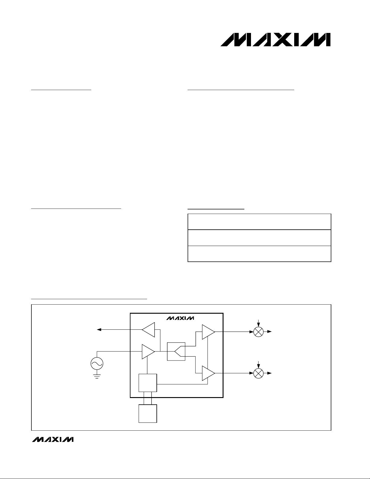
MAX9987
MAX9988
BIAS
BIASIN
RF LO
TO PLL
PRESCALER
PLL BUFFER
INPUT AMP
OUTPUT AMP
(2)
OUTPUT AMP
(1)
RF INPUT
(1)
IF OUTPUT
(1)
PASSIVE TWO-WAY
POWER SPLITTER
IN
(+7dBm)
OUTPLL
(+3dBm)
OUT1
(+17dBm)
OUT2
(+17dBm)
BIASOUT
BIAS
CONTROL
NETWORK
RF INPUT
(2)
IF OUTPUT
(2)
Typical Operating Circuit and Block Diagram
Ordering Information
19-2416; Rev 2; 3/04
For pricing, delivery, and ordering information, please contact Maxim/Dallas Direct! at
1-888-629-4642, or visit Maxim’s website at www.maxim-ic.com.
PART
TEMP
RANGE
PIN-
FREQUENCY
RANGE
MAX9987ETP-T
20 Thin
700MHz to
1100MHz
MAX9988ETP-T
20 Thin
1500MHz to
2200MHz
*EP = Exposed paddle.
PACKAGE
-40°C to 85°C
-40°C to 85°C
QFN-EP*
QFN-EP*
MAX9987/MAX9988
+14dBm to +20dBm LO Buffers/Splitters
with ±1dB Variation
2 _______________________________________________________________________________________
ABSOLUTE MAXIMUM RATINGS
Stresses beyond those listed under “Absolute Maximum Ratings” may cause permanent damage to the device. These are stress ratings only, and functional
operation of the device at these or any other conditions beyond those indicated in the operational sections of the specifications is not implied. Exposure to
absolute maximum rating conditions for extended periods may affect device reliability.
VCC1, VCC2, VCC3,
VCCREF to GND.................................................-0.3V to +6.0V
IN to GND...................................................-0.3V to (V
CC
+ 0.3V)
OUT1, OUT2,
OUTPLL to GND......................................-0.3V to (V
CC
+ 0.3V)
REF to GND ......................................................Source/Sink 5mA
INBIAS, OUTBIAS, to GND..................................-0.3V to +0.75V
PLLBIAS ......................................................................Sink 25mA
RF Input Power...............................................................+20dBm
Continuous Power Dissipation (T
A
= +70°C)
5mm
✕
5mm 20-Pin Thin QFN (derate 20mW/°C
above +70°C).............................................................1600mW
θJA....................................................................................50°C/W
Junction Temperature......................................................+150°C
Operating Temperature Range ...........................-40°C to +85°C
Storage Temperature Range .............................-65°C to +150°C
Lead Temperature (soldering, 10s) .................................+300°C
DC ELECTRICAL CHARACTERISTICS—MAX9987
(Typical Application Circuit, VCC= 4.75V to 5.25V, input and outputs terminated in 50Ω, TA= -40°C to +85°C. Typical specifications
are for V
CC
= 5.0V and TA= +25°C.) (Note 1)
PARAMETER
CONDITIONS
UNITS
Supply Voltage V
CC
V
Low power setting
(see Table 1 for resistor values)
Nominal power setting
(R
1
, R2, R4, and R5 not installed)
171Supply Current I
CC
High power setting
(see Table 1 for resistor values)
mA
DC ELECTRICAL CHARACTERISTICS—MAX9988
(Typical Application Circuit, VCC= 4.75V to 5.25V, input and outputs terminated in 50Ω, TA= -40°C to +85°C. Typical specifications
are for V
CC
= 5.0V and TA= +25°C.) (Note 1)
PARAMETER
CONDITIONS
UNITS
Supply Voltage V
CC
V
Low power setting
(see Table 1 for resistor values)
Nominal power setting
(R
1
, R2, R4, and R5 not installed)
175Supply Current I
CC
High power setting
(see Table 1 for resistor values)
mA
SYMBOL
MIN TYP MAX
4.75 5.00 5.25
110
SYMBOL
139 155
221
MIN TYP MAX
4.75 5.00 5.25
120
150 162
229

MAX9987/MAX9988
+14dBm to +20dBm LO Buffers/Splitters
with ±1dB Variation
_______________________________________________________________________________________ 3
AC ELECTRICAL CHARACTERISTICS—MAX9987
(Typical Application Circuit, VCC= 4.75V to 5.25V, 50Ω environment, +4dBm < PIN< +10dBm, 700MHz < fIN< 1100MHz,
T
A
= -40°C to +85°C, unless otherwise noted. Typical specifications are for VCC= 5.0V, PIN= +7dBm, fIN= 900MHz, and
T
A
= +25°C, unless otherwise noted.) (Note 1)
PARAMETER
CONDITIONS
UNITS
Operating Frequency f
MHz
Low power setting, PIN = +4dBm
(see Table 1 for resistor values)
Nominal power setting,
+4dBm < P
IN
< +10dBm, 4.75V < VCC <
5.25V, -40°C < T
A
< +85°C
(R
1
, R2, R4, and R5 not installed)
17.3
Output Power (Main Drivers) P
OUTLO
High power setting, PIN = +10dBm
(see Table 1 for resistor values)
dBm
Output Power (PLL Driver)
3.7
dBm
Input VSWR VSWR
IN
Output VSWR
Output-Noise Power Density P
NOISE
V
CC
= 5.0V, ±100MHz offset
(R
1
, R2, R4, and R5 not installed)
dBm/Hz
OUT1 to OUT2 Isolation S23
V
CC
= 5.0V, nominal power setting
(R
1
, R2, R4, and R5 not installed)
45 dB
OUT2 to OUT1 Isolation S32
V
CC
= 5.0V, nominal power setting
(R
1
, R2, R4, and R5 not installed)
39 dB
OUT1 to RFIN Isolation S12
V
CC
= 5.0V, nominal power setting
(R
1
, R2, R4, and R5 not installed)
48 dB
OUT2 to RFIN Isolation S13
V
CC
= 5.0V, nominal power setting
(R
1
, R2, R4, and R5 not installed)
50 dB
SYMBOL
P
OUTPLL
VSWR
OUT
MIN TYP MAX
700 1100
14.3
±0.8
19.7
1.2:1
1.7:1
-152
MAX9987/MAX9988
+14dBm to +20dBm LO Buffers/Splitters
with ±1dB Variation
4 _______________________________________________________________________________________
PARAMETER
SYMBOL
CONDITIONS
MIN
TYP
MAX
UNITS
Operating Frequency f
MHz
Low power setting, PIN = +6dBm
(see Table 1 for resistor values)
Nominal power setting,
+6dBm < P
IN
< +12dBm, 4.75V < VCC <
5.25V, -40°C < T
A
< +85°C
(R
1
, R2, R4, and R5 not installed)
17.3
Output Power
(Main Drivers)
High power setting, PIN = +12dBm
(see Table 1 for resistor values)
dBm
Output Power
(PLL Driver)
3.6
dBm
Input VSWR
Output VSWR
Output-Noise Power Density
VCC = 5.0V, ±100MHz offset
dBm/Hz
OUT1 to OUT2 Isolation S23
V
CC
= 5.0V, nominal power setting
(R
1
, R2, R4, and R5 not installed)
33 dB
OUT2 to OUT1 Isolation S32
V
CC
= 5.0V, nominal power setting
(R
1
, R2, R4, and R5 not installed)
44 dB
OUT1 to RFIN Isolation S12
V
CC
= 5.0V, nominal power setting
(R
1
, R2, R4, and R5 not installed)
49 dB
OUT2 to RFIN Isolation S13
V
CC
= 5.0V, nominal power setting
(R
1
, R2, R4, and R5 not installed)
47 dB
AC ELECTRICAL CHARACTERISTICS—MAX9988
(Typical Application Circuit, VCC= 4.75V to 5.25V, 50Ω environment, +6dBm < PIN< +12dBm, 1500MHz < fIN< 2200MHz, and
T
A
= -40°C to +85°C, unless otherwise noted. Typical specifications are for VCC= 5.0V, PIN= +9dBm, fIN= 1800MHz, and
T
A
= +25°C unless otherwise noted.) (Note 1)
Note 1: Devices are 100% DC screened and AC production tested for functionality. Data sheet typical specifications are derived
from the average of 30 units from a typical lot, and are tested under the conditions specified for the typical specifications.
1500 2200
14.2
P
OUTLO
P
OUTPLL
VSWR
VSWR
P
NOISE
OUT
IN
±0.8
19.5
1.5:1
1.4:1
-152

MAX9987/MAX9988
+14dBm to +20dBm LO Buffers/Splitters
with ±1dB Variation
_______________________________________________________________________________________ 5
SUPPLY CURRENT vs. OUTPUT POWER
OUTMAIN
MAX9987 toc01
OUTPUT POWER (dBm)
SUPPLY CURRENT (mA)
20151050-5-10
145
150
155
160
165
170
180
140
-15
175
TA = -40°C
TA = +25°C AND +85°C
OUTPUT POWER vs. INPUT POWER
OUT1
MAX9987 toc02
INPUT POWER (dBm)
OUTPUT POWER (dBm)
923-3-4
11
12
13
14
15
16
17
18
19
20
10
-5 10
87-2 -1 0 1 4 5 6
TA = +85°C
TA = +25°C
TA = -40°C
OUTPUT POWER vs. INPUT POWER
OUT2
MAX9987 toc03
INPUT POWER (dBm)
OUTPUT POWER (dBm)
923-3-4
11
12
13
14
15
16
17
18
19
20
10
-5 10
87-2 -1 0 1 4 5 6
TA = +85°C
TA = +25°C
TA = -40°C
OUTPUT POWER vs. INPUT POWER, OUTPLL
MAX9987 toc04
INPUT POWER (dBm)
OUTPUT POWER (dBm)
862 4-2 0-4
-4
-3
-2
-1
0
1
2
3
4
5
-5
-6 10
TA = +85°C
TA = +25°C
TA = -40°C
OUTPUT POWER vs. FREQUENCY, OUT1
MAX9987 toc05
OPERATING FREQUENCY (MHz)
OUTPUT POWER (dBm)
1200800700600
15
16
17
18
20
14
500
19
900 1000 1100
TA = +85°C
TA = +25°C
TA = -40°C
OUTPUT POWER vs. FREQUENCY, OUT2
MAX9987 toc06
OPERATING FREQUENCY (MHz)
OUTPUT POWER (dBm)
1200800700600
15
16
17
18
20
14
500
19
900 1000 1100
TA = +85°C
TA = +25°C
TA = -40°C
OUTPUT POWER vs. FREQUENCY, PLL
MAX9987 toc07
OPERATING FREQUENCY (MHz)
OUTPUT POWER (dBm)
1200800700600
1
2
3
4
6
0
500
5
900 1000 1100
TA = +85°C
TA = +25°C
TA = -40°C
OUTPUT POWER AND SUPPLY CURRENT
vs. TEMPERATURE
MAX9987 toc08
AMBIENT TEMPERATURE (°C)
OUTPUT POWER (dBm)
806020 400-20
16.2
16.4
16.6
16.8
17.0
17.2
17.4
17.6
17.8
18.0
16.0
-40
I
CC
160.2
160.4
160.6
160.8
161.0
161.2
161.4
161.6
161.8
162.0
160.0
SUPPLY CURRENT (mA)
P
OUT
OUTPUT POWER vs. SUPPLY VOLTAGE
MAX9987 toc09
SUPPLY VOLTAGE (V)
OUT1, OUT2 OUTPUT POWER (dBm)
5.54.94.84.74.6
14.5
15.0
15.5
16.0
16.5
17.0
18.0
14.0
4.5
17.5
OUT2
5.0 5.1 5.2
5.3
5.4
2.5
3.0
3.5
4.0
4.5
5.0
6.0
2.0
5.5
OUT1
OUTPLL
PLL OUTPUT POWER (dBm)
Typical Operating Characteristics
(VCC= 5.0V, nominal bias, fIN= 900MHz, PIN= +7dBm, TA= +25°C, unless otherwise noted.) (Shaded regions are outside the
guaranteed operating range, and are provided for reference only.)
MAX9987

MAX9987/MAX9988
+14dBm to +20dBm LO Buffers/Splitters
with ±1dB Variation
6 _______________________________________________________________________________________
Typical Operating Characteristics (continued)
(VCC= 5.0V, nominal bias, fIN= 900MHz, PIN= +7dBm, TA= +25°C, unless otherwise noted.) (Shaded regions are outside the
guaranteed operating range, and are provided for reference only.)
SUPPLY CURRENT vs. SUPPLY VOLTAGE
MAX9987 toc10
SUPPLY VOLTAGE (V)
SUPPLY CURRENT (mA)
5.54.94.84.74.6
145
150
155
160
170
140
4.5
165
5.0 5.1 5.2
5.3
5.4
PLL NOT BIASED
PLL BIASED
SMALL-SIGNAL GAIN vs. FREQUENCY
MAX9987 toc11
FREQUENCY (GHz)
GAIN (dB)
1.00.90.80.70.6
14
15
16
17
18
19
13
0.5 1.1
VCC = 5.0V
T
A
= +25°C
P
IN
= -15dBm
NOMINAL BIAS
OUT1
OUT2
INPUT RETURN LOSS vs. FREQUENCY
MAX9987 toc12
FREQUENCY (GHz)
RETURN LOSS (dB)
1.11.00.90.80.70.6
-35
-30
-25
-20
-15
-10
0
-40
0.5
-5
VCC = 5.0V
T
A
= +25°C
P
IN
= +7dBm
OUTPUT RETURN LOSS vs. FREQUENCY
MAX9987 toc13
FREQUENCY (GHz)
RETURN LOSS (dB)
1.11.00.90.80.70.6
-18
-16
-14
-12
-10
-8
-4
-20
0.5
-6
VCC = 5.0V
T
A
= +25°C
P
IN
= +7dBm
-2
0
OUT2
OUT1
PLL
IN ISOLATION vs. FREQUENCY
MAX9987 toc14
FREQUENCY (GHz)
ISOLATION (dB)
1.11.00.90.80.70.6
-65
-60
-55
-50
-45
-40
-30
-70
0.5
-35
VCC = 5.0V
T
A
= +25°C
P
IN
= +7dBm
-25
-20
OUT2 TO IN
PLL TO IN
OUT1 TO IN
OUT1 AND OUT2 ISOLATION vs. FREQUENCY
MAX9987 toc15
FREQUENCY (GHz)
ISOLATION (dB)
1.11.00.90.80.70.6
-65
-60
-55
-50
-45
-40
-30
-70
0.5
-35
VCC = 5.0V
T
A
= +25°C
P
IN
= +7dBm
-25
-20
OUT1 TO OUT2
OUT2 TO OUT1
PLL ISOLATION vs. FREQUENCY
MAX9987 toc16
FREQUENCY (GHz)
ISOLATION (dB)
1.11.00.90.80.70.6
-65
-60
-55
-50
-45
-40
-30
-70
0.5
-35
VCC = 5.0V
T
A
= +25°C
P
IN
= +7dBm
-25
-20
OUT2 TO PLL
OUT1 TO PLL
PLL TO OUT_
OUTPUT NOISE POWER
vs. INPUT POWER
MAX9987 toc17
INPUT POWER (dBm)
NOISE POWER (dBm/Hz)
98765
-155
-150
-145
-140
-160
410
±100MHz OFFSET
MAX9987

MAX9987/MAX9988
+14dBm to +20dBm LO Buffers/Splitters
with ±1dB Variation
_______________________________________________________________________________________ 7
140
150
145
160
155
175
170
165
180
-15 -5-10 0 5 10 15 20
SUPPLY CURRENT vs. OUTPUT POWER
MAX9988 toc01
OUTPUT POWER (dBm)
SUPPLY CURRENT (mA)
TA = +25°C
TA = +85°C
TA = -40°C
OUTPUT POWER vs. INPUT POWER, OUT1
MAX9988 toc02
INPUT POWER (dBm)
OUTPUT POWER (dBm)
8756-2 -1 0 1 2 3 4-4 -3
11
12
13
14
15
16
17
18
19
20
10
-5 9
10
TA = -40°C
TA = +85°C
TA = +25°C
OUTPUT POWER vs. INPUT POWER, OUT2
MAX9988 toc03
INPUT POWER (dBm)
OUTPUT POWER (dBm)
8756-2 -1 0 1 2 3 4-4 -3
11
12
13
14
15
16
17
18
19
20
10
-5 9
10
TA = -40°C
TA = +25°C
TA = +85°C
-5
-3
-4
-1
-2
1
0
2
4
3
5
-6 -2 0-4 246810
OUTPUT POWER vs. INPUT POWER, OUTPLL
MAX9988 toc04
INPUT POWER (dBm)
OUTPUT POWER (dBm)
TA = +25°C AND +85°C
TA = -40°C
10
13
12
11
15
14
19
18
17
16
20
1500 1600 1700 1800 1900 2000 2100 2200
OUTPUT POWER vs. FREQUENCY, OUT1
MAX9988 toc05
OPERATING FREQUENCY (MHz)
OUTPUT POWER (dBm)
TA = +85°C
TA = +25°C
TA = -40°C
10
13
12
11
15
14
19
18
17
16
20
1500 1600 1700 1800 1900 2000 2100 2200
OUTPUT POWER vs. FREQUENCY, OUT2
MAX9988 toc06
OPERATING FREQUENCY (MHz)
OUTPUT POWER (dBm)
TA = +85°C
TA = +25°C
TA = -40°C
0
2
1
4
3
5
6
1500 1800 19001600 1700 2000 2100 2200
OUTPUT POWER vs. FREQUENCY, OUTPLL
MAX9988 toc07
OPERATING FREQUENCY (MHz)
OUTPUT POWER (dBm)
TA = +85°C
TA = +25°C
TA = -40°C
15.0
16.4
16.2
16.0
15.8
15.6
15.4
15.2
16.8
16.6
17.2
17.0
17.4
17.8
17.6
18.0
OUTPUT POWER AND SUPPLY CURRENT
vs. TEMPERATURE
MAX9988 toc08
AMBIENT TEMPERATURE (°C)
OUTPUT POWER (dBm)
-40 0 20-20 40 60 80
160
174
172
170
168
166
164
162
178
176
182
180
184
188
186
190
SUPPLY CURRENT (mA)
I
CC
P
OUT
14.0
15.0
14.5
15.5
17.0
17.5
16.5
16.0
18.0
4.5 4.7 4.8 4.9 5.04.6 5.1 5.2 5.3 5.4 5.5
OUTPUT POWER vs. SUPPLY VOLTAGE
MAX9988 toc09
SUPPLY VOLTAGE (V)
OUT1, OUT2 OUTPUT POWER (dBm)
2.0
3.0
2.5
3.5
5.0
5.5
4.5
4.0
6.0
PLL OUTPUT POWER (dBm)
OUT2
OUT1
OUTPLL
_______________________________________________________________________________________ 7
Typical Operating Characteristics (continued)
(VCC= 5.0V, nominal bias, fIN= 1800MHz, PIN= +7dBm, TA= +25°C, unless otherwise noted.) (Shaded regions are outside the
guaranteed operating range, and are provided for reference only.)
MAX9988

MAX9987/MAX9988
+14dBm to +20dBm LO Buffers/Splitters
with ±1dB Variation
8 _______________________________________________________________________________________
150
165
160
155
170
175
180
4.5 4.94.84.6 4.7 5.0 5.1 5.2 5.3 5.4 5.5
SUPPLY CURRENT
vs. SUPPLY VOLTAGE
MAX9988 toc10
SUPPLY VOLTAGE (V)
SUPPLY CURRENT (mA)
PLL BIASED
PLL NOT BIASED
10
12
11
14
13
17
16
15
18
1.5 1.71.6 1.8 1.9 2.0 2.1 2.2
SMALL-SIGNAL GAIN vs. FREQUENCY
MAX9988 toc11
FREQUENCY (GHz)
GAIN (dB)
VCC = 5.0V
T
A
= +25°C
P
IN
= -15dBm
NORMAL BIAS
OUT2
OUT1
-20
-16
-18
-12
-14
-8
-10
-6
1.5 1.7 1.81.6 1.9 2.0 2.1 2.2
INPUT RETURN LOSS vs. FREQUENCY
MAX09988 toc12
FREQUENCY (GHz)
RETURN LOSS (dB)
VCC = 5.0V
T
A
= +25°C
P
IN
= +7dBm
-40
-30
-35
-20
-25
-5
-10
-15
0
1.5 1.71.6 1.8 1.9 2.0 2.1 2.2
OUTPUT RETURN LOSS vs. FREQUENCY
MAX9988 toc13
FREQUENCY (GHz)
RETURN LOSS (dB)
VCC = 5.0V
T
A
= +25°C
P
IN
= +7dBm
OUT2
OUT1
OUTPLL
-65
-50
-55
-60
-40
-45
-20
-25
-30
-35
-15
1.5 1.6 1.7 1.8 1.9 2.0 2.1 2.2
OUT TO IN ISOLATION vs. FREQUENCY
MAX9988 toc14
FREQUENCY (GHz)
ISOLATION (dB)
VCC = 5.0V
T
A
= +25°C
P
IN
= +7dBm
OUT1 TO IN
OUT2 TO IN
PLL TO IN
-65
-50
-55
-60
-40
-45
-20
-25
-30
-35
-15
1.5 1.6 1.7 1.8 1.9 2.0 2.1 2.2
OUT TO OUT ISOLATION vs. FREQUENCY
MAX9988 toc15
FREQUENCY (GHz)
ISOLATION (dB)
VCC = 5.0V
T
A
= +25°C
P
IN
= +7dBm
OUT1 TO OUT2
OUT2 TO OUT1
-50
-35
-40
-45
-25
-30
-5
-10
-15
-20
0
1.5 1.6 1.7 1.8 1.9 2.0 2.1 2.2
PLL ISOLATION vs. FREQUENCY
MAX9988 toc16
FREQUENCY (GHz)
ISOLATION (dB)
VCC = 5.0V
T
A
= +25°C
P
IN
= +7dBm
OUT2 TO PLL
PLL TO OUT_
OUT1 TO PLL
-140
-145
-150
-155
-160
4756 8910
OUTPUT NOISE vs. INPUT POWER
MAX9988 toc17
INPUT POWER (dBm)
OUTPUT NOISE (dBm/Hz)
±100MHz OFFSET
Typical Operating Characteristics (continued)
(VCC= 5.0V, nominal bias, fIN= 1800MHz, PIN= +7dBm, TA= +25°C, unless otherwise noted.) (Shaded regions are outside the
guaranteed operating range, and are provided for reference only.)
MAX9988

MAX9987/MAX9988
+14dBm to +20dBm LO Buffers/Splitters
with ±1dB Variation
_______________________________________________________________________________________ 9
Detailed Description
The MAX9987/MAX9988 LO amplifiers/splitters each
consist of a single input amplifier, a two-way passive
power splitter, two separate output amplifiers, as well as
a third buffer amplifier to drive the LO’s PLL. The bias
currents for the amplifiers are adjustable through off-chip
resistors. This allows the output level to be precision set
anywhere from +14dBm to +20dBm. The PLL output is
preset to +3dBm (about 900mV
P-P
into 50Ω).
Power levels are typically ±1dB over the full supply, input
power, frequency, and temperature range. Precision
power control is achieved by internal control circuitry.
Maintaining tight power control keeps the system engineer from over specifying the LO drive in order to guarantee a linearity specification in the base-station mixer.
More than 40dB isolation between the LO outputs and
the input prevents VCO pulling, and the 30dB outputto-output isolation reduces branch-to-branch coupling.
The MAX9987 is specified from 700MHz to 1100MHz,
and the MAX9988 is specified from 1500MHz to
2200MHz. Both are offered in compact 5mm
✕
5mm 20-
pin QFN packages with exposed paddle.
Input Amplifier
A single low-noise input amplifier before the passive
splitter provides gain and isolation. The compressed
output power for this stage is controlled by the bias setting resistors R1or R4(see Typical Application Circuit).
These resistors are not required for the nominal +17dBm
output; see Table 1 for bias resistor values to obtain
+14dBm to +20dBm output power.
The input is internally matched to 50Ω, and typical
VSWR is no more than 2:1 over all operating conditions.
Since the input is internally biased, provide a DC block
at the input pin.
PLL Amplifier and Output
A small amount of power is tapped off from the input
amplifier’s output, and fed to a high-isolation buffer to
drive the PLL output at +3dBm. If the PLL output is not
required, it can be disabled by removing R3; disabling
the PLL output saves 12mA supply current.
Passive Two-Way Splitter
The input amplifier drives an integrated power splitter.
All impedance matching between stages is on-chip, so
no external tuning components are required.
Pin Description
PIN NAME FUNCTION
1, 4, 8, 9, 13,
17, 18, EP
GND Ground
2INInput. Internally matched 50Ω RF input. AC couple to this pin.
3
Supply. Supply connection for on-chip voltage and current references. See Applications Information
for information on decoupling.
5 REF
Voltage Reference Output. Output for on-chip 1.5V bandgap voltage reference. See
Applications Information section for information on decoupling.
6 BIASIN
Bias Connection for Input Buffer. Set compressed power point for input amplifier with a resistor to
REF or GND. For +17dBm output power, no external biasing resistors are required. See Applications
Information section for information.
7
Bias Connection for Output Amplifiers. Set compressed power point for OUT1 and OUT2 with a
resistor to REF or ground. For +17dBm output power, no external biasing resistors are required. See
Applications Information section for information.
10 OUT2 Output 2. Internally matched 50Ω RF output. AC couple to this pin.
11, 12 VCC3 Supply. Supply connection for OUT2.
14, 15 VCC2 Supply. Supply connection for OUT1.
16 OUT1 Output 1. Internally matched 50Ω RF output. AC couple to this pin.
19 VCC1 Supply. Supply connection for input amplifier.
20 OUTPLL Output PLL. Output for driving optional external PLL.
VCCREF
BIASOUT

MAX9987/MAX9988
+14dBm to +20dBm LO Buffers/Splitters
with ±1dB Variation
10 ______________________________________________________________________________________
Driver Amplifiers and Outputs
Each of the output amplifiers are similar to the input
amplifier, except they are biased higher to provide more
output power. For example, with an input power of
+10dBm, the MAX9987 can deliver +20dBm at both outputs. The bias is adjustable; see Table 1 for details.
Both RF outputs are internally matched to 50Ω, with a
typical VSWR limit of 2:1. Provide DC blocking capacitors
at the outputs.
Applications Information
Input and Output Matching
All input and output matching is accomplished on-chip;
no external matching circuitry is required. Use a DC
block of about 47pF (lowband) or 22pF (highband) at the
input and the outputs. Because these parts are internally
broadband matched, adjusting external component
values can optimize performance for a particular band.
Input Drive Level
In the case of the MAX9987, the typical required input
drive level is +7dBm for +17dBm output, or +10dBm for
+20dBm output. The MAX9988 uses slightly higher
input levels (see Table 1). The typical VCO cannot provide sufficient drive by itself; the typical application follows the VCO with attenuation (about +3dB), and then
with a low-noise gain block. This allows the VCO to
drive the MAX9987/MAX9988 input at the required level
without being load-pulled.
Output Drive Level
The output drive of the MAX9987/MAX9988 is nominally
+17dBm ±1dB. This is the typical application, with no
external bias-setting resistors at INBIAS and OUTBIAS.
Output power can be set from +14dBm to +20dBm by
using the bias-setting resistor values listed in Table 1.
Layout Considerations
A properly designed PC board is an essential part of
any RF/microwave circuit. Keep RF signal lines as short
as possible to reduce losses, radiation, and inductance. For best performance, route the ground pin
traces directly to the exposed pad underneath the
package. This pad must be connected to the ground
plane of the board by using multiple vias under the
device to provide the best RF/thermal conduction path.
Solder the exposed pad on the bottom of the device
package to a PC board exposed pad.
Chip Information
TRANSISTOR COUNT: 89
PROCESS: BiCMOS
Table 1. External Resistor Values for +14dBm to +20dBm Output Power
NOMINAL
OUTPUT POWER
(dBm)
R
1
(Ω)R
2
(Ω)R
4
(Ω)R
5
(Ω)
MAX9987
INPUT DRIVE
(dBm)
MAX9988
INPUT DRIVE
(dBm)
+20 1.35k 2.0k Open Open 10 ±3 12 ±3
+19 2.2k 3.0k Open Open 9 ±3 11 ±3
+18 5.0k 6.0k Open Open 8 ±3 10 ±3
+17 Open Open Open Open 7 ±3 9 ±3
+16 Open Open 1.8k 3.0k 6 ±3 8 ±3
+15 Open Open 0.9k 1.1k 5 ±3 7 ±3
+14 Open Open 0.6k 0.6k 4 ±3 6 ±3
Table 2. Component Values for Typical
Application Circuit
COMPONENT VALUE
DESIGNATION
MAX9987
(LOWBAND)
MAX9988
(HIGHBAND)
C1, C6 100nF 100nF
C3 100pF 100nF
C2, C4, C5, C7, C8,
C9, C12, C13, C14
47pF 22pF
C10, C11 5pF 10pF
R1, R2, R4, R5 See Table 1 See Table 1
R3 100Ω 100Ω

MAX9987/MAX9988
+14dBm to +20dBm LO Buffers/Splitters
with ±1dB Variation
______________________________________________________________________________________ 11
MAX9987
MAX9988
1
2
3
4
5
6
789
10
20
19 18 17 16
15
14
13
12
11
BIAS
R4* R5*
GND
BIASOUT
BIASIN
GND
GND
VCC1
OUTPLL
GND
OUT2 OUT1
R2*
C8
C13
C10
VCC3
VCC3
VCC2
VCC2
GND
GND
IN
VCCREF
GND
REF
C9
5.0V
C1
R3
100Ω
C2
C6
C7
C14
C5
OUT TO PLL
(+3dBm)
INPUT FROM LO
5.0V
5.0V
5.0V
TO OUTPUT 2
TO OUTPUT 1
R1*
C11 C12
C3
C4
5.0V
* FOR THESE VALUES, SEE TABLE 1.
FOR CAPACITOR VALUES, SEE TABLE 2.
EXPOSED PAD
Typical Application Circuit/Pin Configuration

MAX9987/MAX9988
+14dBm to +20dBm LO Buffers/Splitters
with ±1dB Variation
Maxim cannot assume responsibility for use of any circuitry other than circuitry entirely embodied in a Maxim product. No circuit patent licenses are
implied. Maxim reserves the right to change the circuitry and specifications without notice at any time.
12 ____________________Maxim Integrated Products, 120 San Gabriel Drive, Sunnyvale, CA 94086 408-737-7600
© 2004 Maxim Integrated Products Printed USA is a registered trademark of Maxim Integrated Products.
Package Information
(The package drawing(s) in this data sheet may not reflect the most current specifications. For the latest package outline information,
go to www.maxim-ic.com/packages.)
32L QFN.EPS
 Loading...