

Page 1
General Description
The MAX9985 high-linearity, dual-channel downconversion mixer is designed to provide approximately 6dB
gain, +28.5dBm of IIP3, and 10.5dB of noise figure (NF)
ideal for diversity receiver applications. With a 700MHz
to 1000MHz RF frequency range and a 570MHz to
865MHz LO frequency range, this mixer is ideal for lowside LO injection architectures. In addition, the broad
frequency range makes the MAX9985 ideal for GSM
850/950, 2G/2.5G EDGE, WCDMA, cdma2000
®
, and
iDEN®base-station applications.
The MAX9985 dual-channel downconverter achieves a
high level of component integration. The MAX9985 integrates two double-balanced active mixer cores, two LO
buffers, a dual-input LO selectable switch, and a pair of
differential IF output amplifiers. In addition, integrated
on-chip baluns at the RF and LO ports allow for singleended RF and single-ended LO inputs. The MAX9985
requires a typical 0dBm LO drive. Supply current is
adjustable up to 400mA.
The MAX9985 is available in a 36-pin thin QFN package (6mm x 6mm) with an exposed paddle. Electrical
performance is guaranteed over the extended temperature range, from TC= -40°C to +85°C.
Applications
850MHz WCDMA Base Stations
GSM 850/GSM 950, 2G/2.5G EDGE Base
Stations
cdmaOne™ and cdma2000 Base Stations
iDEN Base Stations
Fixed Broadband Wireless Access
Wireless Local Loop
Private Mobile Radios
Military Systems
Digital and Spread-Spectrum Communication
Systems
Microwave Links
Features
700MHz to 1000MHz RF Frequency Range
570MHz to 865MHz LO Frequency Range
50MHz to 250MHz IF Frequency Range
6dB Typical Conversion Gain
10.5dB Typical Noise Figure
+28.5dBm Typical Input IP3
+16.2dBm Typical Input 1dB Compression Point
77dBc Typical 2RF-2LO Spurious Rejection at
P
RF
= -10dBm
Dual Channels Ideal for Diversity Receiver
Applications
47dB Typical Channel-to-Channel Isolation
-3dBm to +3dBm LO Drive
Integrated LO Buffer
Internal RF and LO Baluns for Single-Ended
Inputs
Built-In SPDT LO Switch with 43dB LO1-to-LO2
Isolation and 50ns Switching Time
Pin-Compatible with MAX9995/MAX9995A
1700MHz to 2200MHz Mixers
Lead-Free Package Available
MAX9985
Dual, SiGe, High-Linearity, 700MHz to 1000MHz
Downconversion Mixer with LO Buffer/Switch
________________________________________________________________
Maxim Integrated Products
1
Ordering Information
19-0705 Rev 0; 1/07
For pricing, delivery, and ordering information, please contact Maxim/Dallas Direct! at
1-888-629-4642, or visit Maxim’s website at www.maxim-ic.com.
*
EP = Exposed paddle.
T = Tape-and-reel package.
+
Denotes lead-free and RoHS compliant.
cdma2000 is a registered trademark of Telecommunications
Industry Association.
iDEN is a registered trademark of Motorola, Inc.
cdmaOne is a trademark of CDMA Development Group.
EVALUATION KIT
AVAILABLE
PART TEMP RANGE PIN-PACKAGE
MAX9985ETX -40°C to +85°C
MAX9985ETX-T -40°C to +85°C
MAX9985ETX+ -40°C to +85°C
MAX9985ETX+T -40°C to +85°C
36 Thi n QFN- E P *
(6mm x 6mm)
36 Thi n QFN- E P *
(6mm x 6mm),
T/R
36 Thi n QFN- E P *
(6mm x 6mm),
lead free, bulk
36 Thi n QFN- E P *
(6mm x 6mm),
lead free, T/R
PKG
CODE
T3666-2
T3666-2
T3666-2
T3666-2
Page 2
MAX9985
Dual, SiGe, High-Linearity, 700MHz to 1000MHz
Downconversion Mixer with LO Buffer/Switch
2 _______________________________________________________________________________________
ABSOLUTE MAXIMUM RATINGS
DC ELECTRICAL CHARACTERISTICS
(Using the
Typical Application Circuit
, no input RF or LO signals applied, VCC= 4.75V to 5.25V, TC= -40°C to +85°C. Typical values
are at V
CC
= 5.0V, TC= +25°C, unless otherwise noted.)
Stresses beyond those listed under “Absolute Maximum Ratings” may cause permanent damage to the device. These are stress ratings only, and functional
operation of the device at these or any other conditions beyond those indicated in the operational sections of the specifications is not implied. Exposure to
absolute maximum rating conditions for extended periods may affect device reliability.
VCCto GND...........................................................-0.3V to +5.5V
LO1, LO2 to GND ...............................................................±0.3V
Any Other Pins to GND...............................-0.3V to (V
CC
+ 0.3V)
RFMAIN, RFDIV, and LO_ Input Power ..........................+20dBm
RFMAIN, RFDIV Current (RF is DC shorted to GND through
balun) ...............................................................................50mA
Continuous Power Dissipation (T
C
= +70°C) (Note A)
36-Pin Thin QFN (derate 26mW/°C above +70°C) .........10.8W
Operating Temperature Range ...........................-40°C to +85°C
Maximum Junction Temperature Range..........................+150°C
θ
JA
.................................................................................+38°C/W
θ
JC
...................................................................................7.4°C/W
Storage Temperature Range .............................-65°C to +150°C
Lead Temperature (soldering, 10s) .................................+300°C
AC ELECTRICAL CHARACTERISTICS
(Using the
Typical Application Circuit
, VCC= 4.75V to 5.25V, RF and LO ports are driven from 50Ω sources, PLO= -3dBm to +3dBm,
P
RF
= -5dBm, fRF= 820MHz to 920MHz, fLO= 670MHz to 865MHz, fIF= 100MHz, fRF> fLO, TC= -40°C to +85°C. Typical values are at
V
CC
= 5.0V, PRF= -5dBm, PLO= 0dBm, fRF= 870MHz, fLO= 770MHz, fIF= 100MHz, TC= +25°C, unless otherwise noted.) (Note 1)
Note A: TCis the temperature on the exposed paddle of the package.
Supply Voltage V
Supply Current I
LOSEL Input High Voltage V
LOSEL Input Low Voltage V
LOSEL Input Current IIH and I
PARAMETER SYMBOL CONDITIONS MIN TYP MAX UNITS
CC
Total supply current (see Table 1 for lower
current settings)
CC
VCC (pin 16) 80
VCC (pin 30) 80
IFM+/IFM- (total of both) 105
IFD+/IFD- (total of both) 105
IH
IL
IL
4.75 5 5.25 V
400 440
2V
0.8 V
-10 +10 µA
mA
RF Frequency f
LO Frequency f
IF Frequency f
LO Drive P
Conversion Gain G
Gain Variation over Temperature -0.012 dB/°C
Conversion Gain Flatness
PARAMETER SYMBOL CONDITIONS MIN TYP MAX UNITS
RF
LO
(Note 2) 700 1000 MHz
(Note 2) 570 865 MHz
IF matching components affect the IF
IF
frequency range (Note 2)
(Note 3) -3 +3 dBm
LO
(Note 6) 4.5 6 7.5 dB
C
Fl atness over any one of thr ee fr equency b and s:
= 824MHz to 849MHz
f
RF
f
= 869MHz to 894MHz
RF
= 880MHz to 915MHz
f
RF
50 250 MHz
±0.1 dB
Page 3
MAX9985
Dual, SiGe, High-Linearity, 700MHz to 1000MHz
Downconversion Mixer with LO Buffer/Switch
_______________________________________________________________________________________ 3
AC ELECTRICAL CHARACTERISTICS (continued)
(Using the
Typical Application Circuit
, VCC= 4.75V to 5.25V, RF and LO ports are driven from 50Ω sources, PLO= -3dBm to +3dBm,
P
RF
= -5dBm, fRF= 820MHz to 920MHz, fLO= 670MHz to 865MHz, fIF= 100MHz, fRF> fLO, TC= -40°C to +85°C. Typical values are at
V
CC
= 5.0V, PRF= -5dBm, PLO= 0dBm, fRF= 870MHz, fLO= 770MHz, fIF= 100MHz, TC= +25°C, unless otherwise noted.) (Note 1)
Noise Figure, Single Sideband NF fIF = 190MHz, no blockers present (Note 3) 10.5 13 dB
Noise Figure under Blocking
Condition
Input Compression Point P
Output Compression Point OP
Small-Signal Compression under
Blocking Conditions
Third-Order Input Intercept Point IIP3
Third-Order Input Intercept Point
Variation over Temperature
Third-Order Output Intercept
Point
2RF-2LO Spur 2 x 2
PARAMETER SYMBOL CONDITIONS MIN TYP MAX UNITS
+11dBm blocker tone applied to RF port at
1dB
1dB
OIP3
961MHz, f
f
IFDESIRED
f
BLOCKER
P
= -5dBm, fRF =
RF
870MHz, f
= 871MHz
f
RF1-fRF2
= -5dBm/tone
P
RF
P
= -5dBm/tone, fIF = 100MHz,
RF
f
RF1-fRF2
= 870MHz, f
f
RF
= 770MHz, f
820MHz (Note 3)
= 860MHz, fLO = 670MHz,
RF
= 190MHz,
= 291MHz (Notes 3, 4)
P
BLOCKER
BLOCKER
= 1MHz, fIF = 100MHz,
= 1MHz (Note 3)
SPUR
P
BLOCKER
PRF = -10dBm 63 77
LO
=
= -5dBm 58 72
P
RF
21 26 dB
16.2 dBm
18.5 21.2 dBm
= +8dBm 0.1
= +11dBm 0.25
28.5 dBm
-0.01 dB/°C
32.0 34.5 dBm
dB
dBc
= 870MHz, f
f
3RF-3LO Spur 3 x 3
LO1-to-LO2 Port Isolation
Maximum LO Leakage at RF Port -40 -30 dBm
M axi m um 2LO Leakag e at RF P or t -45 -20 dBm
Maximum LO Leakage at IF Port -30 -20 dBm
Minimum RF-to-IF Isolation 30 45 dB
Minimum Channel-to-Channel
Isolation
RF
= 770MHz, f
803.3MHz (Note 3)
P
LO1
f
LO1-fLO2
= 100MHz (Notes 3, 5)
f
IF
= -10dBm, RFMAIN (RFDIV) power
P
RF
measured at IFDIV (IFMAIN), relative to
IFMAIN (IFDIV), all unused ports terminated
to 50Ω
SPUR
= +3dBm, P
= 1MHz, PRF = -5dBm,
PRF = -10dBm 70 85
LO
=
= -5dBm 60 75
P
RF
= +3dBm,
LO2
dBc
39 43 dB
40 47 dB
Page 4
MAX9985
Dual, SiGe, High-Linearity, 700MHz to 1000MHz
Downconversion Mixer with LO Buffer/Switch
4 _______________________________________________________________________________________
AC ELECTRICAL CHARACTERISTICS (continued)
(Using the
Typical Application Circuit
, VCC= 4.75V to 5.25V, RF and LO ports are driven from 50Ω sources, PLO= -3dBm to +3dBm,
P
RF
= -5dBm, fRF= 820MHz to 920MHz, fLO= 670MHz to 865MHz, fIF= 100MHz, fRF> fLO, TC= -40°C to +85°C. Typical values are at
V
CC
= 5.0V, PRF= -5dBm, PLO= 0dBm, fRF= 870MHz, fLO= 770MHz, fIF= 100MHz, TC= +25°C, unless otherwise noted.) (Note 1)
Note 1: All limits reflect losses of external components. Output measurements taken at IF outputs of the
Typical Application Circuit
.
Note 2: Performance is guaranteed for f
RF
= 820MHz to 920MHz, fLO= 670MHz to 865MHz, and fIF= 100MHz. Operation outside
this range is possible, but with degraded performance of some parameters. See the
Typical Operating Characteristics
.
Note 3: Guaranteed by design and characterization.
Note 4: Measured with external LO source noise filtered so the noise floor is -174dBm/Hz. This specification reflects the effects of all
SNR degradations in the mixer including the LO noise, as defined in Maxim Application Note 2021.
Note 5: Measured at IF port at IF frequency. LOSEL may be in any logic state.
Note 6: Performance at T
C
= -40°C is guaranteed by design.
LO Switching Time
RF Input Impedance 50 Ω
LO Input Impedance 50 Ω
IF Output Impedance Differential 200 Ω
RF Input Return Loss LO on and IF terminated 24 dB
LO Input Return Loss
IF Return Loss RF terminated in 50Ω 20 dB
PARAMETER SYMBOL CONDITIONS MIN TYP MAX UNITS
50% of LOSEL to IF settled within 2 degrees
(Note 3)
LO port selected 35
LO port unselected 36
0.05 1 µs
dB
Page 5
MAX9985
Dual, SiGe, High-Linearity, 700MHz to 1000MHz
Downconversion Mixer with LO Buffer/Switch
_______________________________________________________________________________________
5
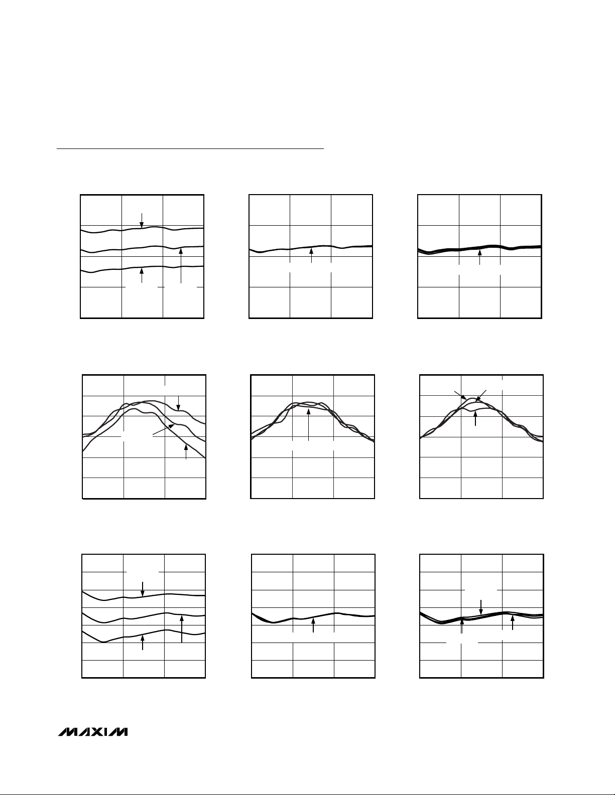
Typical Operating Characteristics
(Using the
Typical Application Circuit
, VCC= 5.0V, PLO= 0dBm, PRF= -5dBm, fRF> fLO, fIF= 100MHz, TC= +25°C, unless other-
wise noted.)
7
6
5
4
8
700 800 900 1000
CONVERSION GAIN vs. RF FREQUENCY
MAX9985 toc01
RF FREQUENCY (MHz)
CONVERSION GAIN (dB)
TC = +85°C
TC = +25°C
TC = -30°C
7
6
5
4
8
700 800 900 1000
CONVERSION GAIN vs. RF FREQUENCY
MAX9985 toc02
RF FREQUENCY (MHz)
CONVERSION GAIN (dB)
PLO = -3dBm, 0dBm, +3dBm
7
6
5
4
8
700 800 900 1000
CONVERSION GAIN vs. RF FREQUENCY
MAX9985 toc03
RF FREQUENCY (MHz)
CONVERSION GAIN (dB)
VCC = 4.75V, 5.0V, 5.25V
24
26
25
28
27
29
30
700 800 900 1000
INPUT IP3 vs. RF FREQUENCY
MAX9985 toc04
RF FREQUENCY (MHz)
INPUT IP3 (dBm)
TC = -30°C
TC = +25°C
TC = +85°C
24
26
25
28
27
29
30
700 800 900 1000
INPUT IP3 vs. RF FREQUENCY
MAX9985 toc05
RF FREQUENCY (MHz)
INPUT IP3 (dBm)
PLO = -3dBm, 0dBm, +3dBm
24
26
25
28
27
29
30
700 800 900 1000
INPUT IP3 vs. RF FREQUENCY
MAX9985 toc06
RF FREQUENCY (MHz)
INPUT IP3 (dBm)
VCC = 5.0V
VCC = 4.75V
VCC = 5.25V
7
9
8
11
10
13
12
14
700 800 900 1000
MAX9985 toc07
RF FREQUENCY (MHz)
NOISE FIGURE (dB)
NOISE FIGURE vs. RF FREQUENCY
TC = -30°C
TC = +25°C
TC = +85°C
7
9
8
11
10
13
12
14
700 800 900 1000
MAX9985 toc08
RF FREQUENCY (MHz)
NOISE FIGURE (dB)
NOISE FIGURE vs. RF FREQUENCY
PLO = -3dBm, 0dBm, +3dBm
7
9
8
11
10
13
12
14
700 800 900 1000
MAX9985 toc09
RF FREQUENCY (MHz)
NOISE FIGURE (dB)
NOISE FIGURE vs. RF FREQUENCY
VCC = 4.75V
VCC = 5.0V
VCC = 5.25V
Page 6

MAX9985
Dual, SiGe, High-Linearity, 700MHz to 1000MHz
Downconversion Mixer with LO Buffer/Switch
6 _______________________________________________________________________________________
Typical Operating Characteristics (continued)
(Using the
Typical Application Circuit
, VCC= 5.0V, PLO= 0dBm, PRF= -5dBm, fRF> fLO, fIF= 100MHz, TC= +25°C, unless other-
wise noted.)
50
60
55
70
65
75
80
700 800 900 1000
2RF-2LO RESPONSE vs. RF FREQUENCY
MAX9985 toc10
RF FREQUENCY (MHz)
2RF-2LO RESPONSE (dBc)
PRF = -5dBm
TC = -30°C
TC = +25°C
TC = +85°C
50
60
55
70
65
75
80
700 800 900 1000
2RF-2LO RESPONSE vs. RF FREQUENCY
MAX9985 toc11
RF FREQUENCY (MHz)
2RF-2LO RESPONSE (dBc)
PRF = -5dBm
PLO = -3dBm
PLO = 0dBm
PLO = +3dBm
50
60
55
70
65
75
80
700 800 900 1000
2RF-2LO RESPONSE vs. RF FREQUENCY
MAX9985 toc12
RF FREQUENCY (MHz)
2RF-2LO RESPONSE (dBc)
PRF = -5dBm
VCC = 4.75V, 5.0V, 5.25V
85
75
65
55
95
700 800 900 1000
3RF-3LO RESPONSE vs. RF FREQUENCY
MAX9985 toc13
RF FREQUENCY (MHz)
3RF-3LO RESPONSE (dBc)
PRF = -5dBm
TC = -30°C
TC = +85°C
TC = +25°C
85
75
65
55
95
700 800 900 1000
3RF-3LO RESPONSE vs. RF FREQUENCY
MAX9985 toc14
RF FREQUENCY (MHz)
3RF-3LO RESPONSE (dBc)
PRF = -5dBm
PLO = -3dBm, 0dBm, +3dBm
85
75
65
55
95
700 800 900 1000
3RF-3LO RESPONSE vs. RF FREQUENCY
MAX9985 toc15
RF FREQUENCY (MHz)
3RF-3LO RESPONSE (dBc)
PRF = -5dBm
VCC = 5.25V
VCC = 4.75V
VCC = 5.0V
19
14
13
16
15
17
18
700 1200
INPUT P
1dB
vs. RF FREQUENCY
MAX9985 toc16
RF FREQUENCY (MHz)
INPUT P
1dB
(dBm)
900800 1000 1100
TC = +25°C
TC = -30°C
TC = +85°C
19
14
13
16
15
17
18
700 1200
INPUT P
1dB
vs. RF FREQUENCY
MAX9985 toc17
RF FREQUENCY (MHz)
INPUT P
1dB
(dBm)
900800 1000 1100
PLO = -3dBm, 0dBm, +3dBm
19
14
13
16
15
17
18
700 1200
INPUT P
1dB
vs. RF FREQUENCY
MAX9985 toc18
RF FREQUENCY (MHz)
INPUT P
1dB
(dBm)
900800 1000 1100
VCC = 5.0V
VCC = 4.75V
VCC = 5.25V
Page 7

MAX9985
Dual, SiGe, High-Linearity, 700MHz to 1000MHz
Downconversion Mixer with LO Buffer/Switch
_______________________________________________________________________________________
7
Typical Operating Characteristics (continued)
(Using the
Typical Application Circuit
, VCC= 5.0V, PLO= 0dBm, PRF= -5dBm, fRF> fLO, fIF= 100MHz, TC= +25°C, unless other-
wise noted.)
_______________________________________________________________________________________
7
CHANNEL ISOLATION vs. RF FREQUENCY
60
55
50
45
TC =
-30°C, +25°C, +85°C
40
CHANNEL ISOLATION (dB)
35
30
700 800 900 1000
RF FREQUENCY (MHz)
LO LEAKAGE AT IF PORT vs. LO FREQUENCY
-10
-15
-20
TC = +25°C
-25
TC = -30°C
60
MAX9985 toc19
MAX9985 toc22
55
50
45
40
CHANNEL ISOLATION (dB)
35
30
-10
-15
-20
-25
CHANNEL ISOLATION vs. RF FREQUENCY
MAX9985 toc20
PLO = -3dBm, 0dBm, +3dBm
700 800 900 1000
RF FREQUENCY (MHz)
LO LEAKAGE AT IF PORT vs. LO FREQUENCY
MAX9985 toc23
PLO = 0dBm
PLO = +3dBm
CHANNEL ISOLATION vs. RF FREQUENCY
60
55
50
45
40
CHANNEL ISOLATION (dB)
35
30
700 800 900 1000
VCC = 4.75V, 5.0V, 5.25V
RF FREQUENCY (MHz)
LO LEAKAGE AT IF PORT vs. LO FREQUENCY
-10
-15
-20
-25
VCC = 5.25V
VCC = 5.0V
MAX9985 toc21
MAX9985 toc24
-30
TC = +85°C
LO LEAKAGE AT IF PORT (dBm)
-35
-40
600 700 750650 800 850 900
LO FREQUENCY (MHz)
RF-TO-IF ISOLATION
vs. RF FREQUENCY
60
55
50
45
40
RF-TO-IF ISOLATION (dB)
35
30
700 800 900 1000
TC = +85°C
TC = +25°C
TC = -30°C
RF FREQUENCY (MHz)
-30
LO LEAKAGE AT IF PORT (dBm)
-35
-40
600 700 750650 800 850 900
60
MAX9985 toc25
55
50
45
40
RF-TO-IF ISOLATION (dB)
35
30
700 800 900 1000
PLO = -3dBm
LO FREQUENCY (MHz)
RF-TO-IF ISOLATION
vs. RF FREQUENCY
PLO = -3dBm, 0dBm, +3dBm
RF FREQUENCY (MHz)
-30
LO LEAKAGE AT IF PORT (dBm)
-35
-40
600 700 750650 800 850 900
60
55
MAX9985 toc26
50
45
40
RF-TO-IF ISOLATION (dB)
35
30
700 800 900 1000
VCC = 4.75V
LO FREQUENCY (MHz)
RF-TO-IF ISOLATION
vs. RF FREQUENCY
VCC = 4.75V, 5.0V, 5.25V
RF FREQUENCY (MHz)
MAX9985 toc27
Page 8

MAX9985
Dual, SiGe, High-Linearity, 700MHz to 1000MHz
Downconversion Mixer with LO Buffer/Switch
8 _______________________________________________________________________________________
Typical Operating Characteristics (continued)
(Using the
Typical Application Circuit
, VCC= 5.0V, PLO= 0dBm, PRF= -5dBm, fRF> fLO, fIF= 100MHz, TC= +25°C, unless other-
wise noted.)
-60
-50
-40
-30
-20
LO LEAKAGE AT RF PORT
vs. LO FREQUENCY
MAX9985 toc28
LO FREQUENCY (MHz)
LO LEAKAGE AT RF PORT (dBm)
500 800 900600 700 1000 1100 1200
TC = +85°C
TC = -30°C
TC = +25°C
-60
-50
-40
-30
-20
LO LEAKAGE AT RF PORT
vs. LO FREQUENCY
MAX9985 toc29
LO FREQUENCY (MHz)
LO LEAKAGE AT RF PORT (dBm)
500 800 900600 700 1000 1100 1200
PLO = -3dBm, 0dBm, +3dBm
-20
-30
-40
-50
-60
600500 900700 800 1000 1100 1200
LO LEAKAGE AT RF PORT
vs. LO FREQUENCY
MAX9985 toc30
LO FREQUENCY (MHz)
LO LEAKAGE AT RF PORT (dBm)
VCC = 4.75V, 5.0V, 5.25V
-60
-50
-30
-40
-20
-10
500 700600 800 900 1000 1100 1200
2LO LEAKAGE AT RF PORT
vs. LO FREQUENCY
MAX9985 toc31
LO FREQUENCY (MHz)
2LO LEAKAGE AT RF PORT (dBm)
TC = +85°C
TC = -30°C
TC = +25°C
-60
-50
-30
-40
-20
-10
500 700600 800 900 1000 1100 1200
2LO LEAKAGE AT RF PORT
vs. LO FREQUENCY
MAX9985 toc32
LO FREQUENCY (MHz)
2LO LEAKAGE AT RF PORT (dBm)
PLO = -3dBm
PLO = +3dBm
PLO = 0dBm
-60
-50
-30
-40
-20
-10
600500 800700 900 1000 1100 1200
2LO LEAKAGE AT RF PORT
vs. LO FREQUENCY
MAX9985 toc33
LO FREQUENCY (MHz)
2LO LEAKAGE AT RF PORT (dBm)
VCC = 4.75V, 5.0V, 5.25V
50
45
40
35
30
600 900700 800 1000 1100 1200
LO SWITCH ISOLATION
vs. RF FREQUENCY
MAX9985 toc34
RF FREQUENCY (MHz)
LO SWITCH ISOLATION (dB)
TC = +85°C
TC = -30°C
TC = +25°C
50
45
40
35
30
600 900700 800 1000 1100 1200
LO SWITCH ISOLATION
vs. RF FREQUENCY
MAX9985 toc35
RF FREQUENCY (MHz)
LO SWITCH ISOLATION (dB)
PLO = -3dBm, 0dBm, 3dBm
50
45
40
35
30
600 900700 800 1000 1100 1200
LO SWITCH ISOLATION
vs. RF FREQUENCY
MAX9985 toc36
RF FREQUENCY (MHz)
LO SWITCH ISOLATION (dB)
VCC = 4.75V, 5.0V, 5.25V
Page 9

MAX9985
Dual, SiGe, High-Linearity, 700MHz to 1000MHz
Downconversion Mixer with LO Buffer/Switch
_______________________________________________________________________________________
9
Typical Operating Characteristics (continued)
(Using the
Typical Application Circuit
, VCC= 5.0V, PLO= 0dBm, PRF= -5dBm, fRF> fLO, fIF= 100MHz, TC= +25°C, unless other-
wise noted.)
30
20
25
10
15
5
0
500 800 900600 700 1000 1100 1200
RF PORT RETURN LOSS
vs. RF FREQUENCY
MAX9985 toc37
RF FREQUENCY (MHz)
RF PORT RETURN LOSS (dB)
PLO = -3dBm, 0dBm, +3dBm
30
20
25
10
15
5
0
0200100 300 400 500
IF PORT RETURN LOSS
vs. IF FREQUENCY
MAX9985 toc38
IF FREQUENCY (MHz)
IF PORT RETURN LOSS (dB)
VCC = 4.75V, 5.0V, 5.25V
50
40
20
30
10
0
500 700600 800 900 1000 1100 1200
LO SELECTED RETURN LOSS
vs. LO FREQUENCY
MAX9985 toc39
LO FREQUENCY (MHz)
LO SELECTED RETURN LOSS (dB)
PLO = +3dBm
PLO = 0dBm
PLO = -3dBm
50
40
20
30
10
0
500 700600 800 900 1000 1100 1200
LO UNSELECTED RETURN LOSS
vs. LO FREQUENCY
MAX9985 toc40
LO FREQUENCY (MHz)
LO UNSELECTED RETURN LOSS (dB)
PLO = -3dBm, 0dBm, +3dBm
360
380
370
400
390
420
410
430
-35 5 25-15 456585
SUPPLY CURRENT
vs. TEMPERATURE (T
C
)
MAX9985 toc41
TEMPERATURE (°C)
SUPPLY CURRENT (mA)
VCC = 5.25V
VCC = 5.0V
VCC = 4.75V
CONVERSION GAIN vs. RF FREQUENCY
(VARIOUS LO AND IF BUFFER BIAS)
MAX9985 toc42
RF FREQUENCY (MHz)
CONVERSION GAIN (dB)
800 900
6.0
6.5
7.0
5.5
700 1000
1
5
6
4
0
2
3
8, 9
7
SEE TABLE 1 FOR R1, R2, AND ICC VALUES.
INPUT IP3 vs. RF FREQUENCY
(VARIOUS LO AND IF BUFFER BIAS)
MAX9985 toc43
RF FREQUENCY (MHz)
INPUT IP3 (dBm)
900800
21
22
23
24
25
26
27
28
29
30
20
700 1000
1
5
6
4
2
0
3
8
9
7
SEE TABLE 1 FOR R1, R2, AND ICC VALUES.
2RF-2LO RESPONSE vs. RF FREQUENCY
(VARIOUS LO AND IF BUFFER BIAS)
RF FREQUENCY (MHz)
2RF-2LO RESPONSE (dBc)
900800
65
70
75
80
85
60
700 1000
5
6
2
3
7
0
SEE TABLE 1 FOR R1, R2, AND ICC VALUES.
PRF = -5dBm
8
MAX9985 toc44
3RF-3LO RESPONSE vs. RF FREQUENCY
(VARIOUS LO AND IF BUFFER BIAS)
MAX9985 toc45
RF FREQUENCY (MHz)
3RF-3LO RESPONSE (dBc)
900800
60
65
70
75
80
85
90
55
700 1000
5
0
4
2
3
7
1
SEE TABLE 1 FOR R1, R2, AND ICC VALUES.
PRF = -5dBm
6
8
9
Page 10

MAX9985
Dual, SiGe, High-Linearity, 700MHz to 1000MHz
Downconversion Mixer with LO Buffer/Switch
10 ______________________________________________________________________________________10 ______________________________________________________________________________________
Typical Operating Characteristics (continued)
(Using the
Typical Application Circuit
, VCC= 5.0V, PLO= 0dBm, PRF= -5dBm, fRF> fLO, fIF= 100MHz, TC= +25°C, unless other-
wise noted.)
INPUT P
1dB
vs. RF FREQUENCY
(VARIOUS LO AND IF BUFFER BIAS)
MAX9985 toc46
RF FREQUENCY (MHz)
INPUT P
1dB
(dBm)
900800
8
9
10
11
12
13
14
15
16
17
18
700 1000
1, 2, 3
4, 5, 6
7, 8, 9
SEE TABLE 1 FOR R1, R2, AND ICC VALUES.
0
LO LEAKAGE AT IF PORT vs. LO FREQUENCY
(VARIOUS VALUES OF L3 AND L6)
MAX9985 toc47
LO FREQUENCY (MHz)
LO LEAKAGE AT IF PORT (dBm)
850800750700650
-35
-30
-25
-20
-15
-10
-40
600 900
0
Ω
L = 7.5nH
L = 30nH
L = 15nH
RF-TO-IF ISOLATION vs. RF FREQUENCY
(VARIOUS VALUES OF L3 AND L6)
MAX9985 toc48
RF FREQUENCY (MHz)
RF-TO-IF ISOLATION (dB)
900800
30
40
50
60
70
20
700 1000
L = 15nH
L = 30nH
L = 7.5nH
0
Ω
Table 1. DC Current vs. Bias Resistor
Settings
BIAS
CONDITION
0 397.8 1070 1100
1 345.0 1400 1100
2 316.5 1400 1620
3 297.5 1400 2210
4 301.2 1910 1100
5 271.7 1910 1620
6 252.2 1910 2210
7 260.1 2800 1100
8 230.5 2800 1620
9 211.5 2800 2210
DC CURRENT
(mA)
R1 AND R4
VALUES (Ω)
R2 AND R5
VALUES (Ω)
Page 11

MAX9985
Dual, SiGe, High-Linearity, 700MHz to 1000MHz
Downconversion Mixer with LO Buffer/Switch
______________________________________________________________________________________ 11______________________________________________________________________________________ 11
Pin Description
PIN NAME FUNCTION
1 RFMAIN Main Channel RF input. Internally matched to 50Ω. Requires an input DC-blocking capacitor.
2 TAPMAIN Main Channel Balun Center Tap. Bypass to GND with capacitors close to the pin.
3, 5, 7, 12,
20, 22, 24,
25, 26, 34
4, 6, 10, 16,
21, 30, 36
8 TAPDIV Diversity Channel Balun Center Tap. Bypass to GND with capacitors close to the pin.
9 RFDIV Diversity Channel RF Input. Internally matched to 50Ω. Requires an input DC-blocking capacitor.
11 IFDBIAS
13, 14 IFD+, IFD-
15 LEXTD
17 LODBIAS
18, 28 N.C. No Connection. Not internally connected.
19 LO1 Local Osci l l ator 1 Inp ut. Thi s i np ut i s i nter nal l y m atched to 50Ω . Req ui r es an i np ut D C - b l ocki ng cap aci tor .
23 LOSEL Local Oscillator Select. Set this pin to high to select LO1. Set low to select LO2.
27 LO2 Local Osci l l ator 2 Inp ut. Thi s i np ut i s i nter nal l y m atched to 50Ω . Req ui r es an i np ut D C - b l ocki ng cap aci tor .
29 LOMBIAS
GND Ground
V
CC
Power Supply. Connect bypass capacitors as close to the pin as possible (see the Typical
Application Circuit).
IF Diversity Amplifier Bias Control. Connect a 1.07kΩ resistor from this pin to ground to set the bias
current for the diversity IF amplifier (see the Typical Operating Characteristics for typical performance
versus resistor value).
Diversity Mixer Differential IF Output. Connect pullup inductors from each of these pins to V
the Typical Application Circuit).
Connect a 30nH inductor from this pin to ground to increase the RF-to-IF and LO-to-IF isolation.
Connect this pin to ground if isolations can be degraded (see the Typical Operating Characteristics
for typical degradation).
LO Diversity Amplifier Bias Control. Connect a 1.1kΩ resistor from this pin to ground to set the bias
current for the diversity LO amplifier (see the Typical Operating Characteristics for typical
performance versus resistor value).
LO Main Amplifier Bias Control. Connect a 1.1kΩ resistor from this pin to ground to set the bias
current for the main LO amplifier (see the Typical Operating Characteristics for typical performance
versus resistor value).
CC
(see
31 LEXTM
32, 33 IFM-, IFM+
35 IFMBIAS
—EP
Connect a 30nH inductor from this pin to ground to increase the RF-IF and LO-IF isolation. Connect
this pin to ground if isolations can be degraded (see the Typical Operating Characteristics for typical
degradation).
Main Mixer Differential IF Output. Connect pullup inductors from each of these pins to V
Typical Application Circuit).
IF M ai n Am p l i fi er Bi as C ontr ol . C onnect a 1.07kΩ r esi stor fr om thi s p i n to g r ound to set the b i as cur r ent for
the m ai n IF am p l i fi er ( see the Typ i cal O p er ati ng C har acter i sti cs for typ i cal p er for m ance vs. r esi stor val ue) .
Exposed Paddle. Solder the exposed paddle to the ground plane using multiple vias. This paddle
affects RF performance and provides heat dissipation.
(see the
CC
Page 12

MAX9985
Detailed Description
The MAX9985 is a dual-channel downconverter
designed to provide 6dB of conversion gain, +28.5dBm
input IP3, and +16.2dBm 1dB input compression point,
with a 10.5dB NF.
In addition to its high-linearity performance, the
MAX9985 achieves a high level of component integration. The device integrates two double-balanced active
mixers for two-channel downconversion. Both the main
and diversity channels include a balun and matching
circuitry to allow 50Ω single-ended interfaces to the RF
ports and the two LO ports. An integrated single-pole,
double-throw (SPDT) switch provides 50ns switching
time between the two LO inputs with 43dB of LO-to-LO
isolation and a -40dBm of LO leakage at the RF port.
Furthermore, the integrated LO buffers provide a high
drive level to each mixer core, reducing the LO drive
required at the MAX9985’s inputs to a -3dBm to +3dBm
range. The IF ports for both channels incorporate differential outputs for downconversion, which is ideal for
providing enhanced IIP2 performance.
Dual-channel downconversion makes the MAX9985
ideal for diversity receiver applications. In addition,
specifications are guaranteed over broad frequency
ranges to allow for use in GSM 850/950, 2G/2.5G
EDGE, WCDMA, cdma2000, and iDEN base stations.
The MAX9985 is specified to operate over a 700MHz to
1000MHz RF input range, a 570MHz to 865MHz LO
range, and a 50MHz to 250MHz IF range. The external
IF components set the lower frequency range (see the
Typical Operating Characteristics
for details).
RF Port and Balun
The RF input ports to both the main and diversity channels are internally matched to 50Ω, requiring no external matching components. A DC-blocking capacitor is
required as the input is internally DC-shorted to ground
through the on-chip balun. The RF port return loss is
typically 15dB over the entire 700MHz to 1000MHz RF
frequency range.
LO Inputs, Buffer, and Balun
The MAX9985 is optimized for a 570MHz to 865MHz
LO frequency range. As an added feature, the
MAX9985 includes an internal LO SPDT switch for use
in frequency-hopping applications. The switch selects
one of the two single-ended LO ports, allowing the
external oscillator to settle on a particular frequency
before it is switched in. LO switching time is typically
less than 50ns, which is more than adequate for typical
GSM applications. If frequency hopping is not
employed, simply set the switch to either of the LO
inputs. The switch is controlled by a digital input
(LOSEL), where logic-high selects LO1 and logic-low
selects LO2. LO1 and LO2 inputs are internally
matched to 50Ω, requiring only an 82pF DC-blocking
capacitor. To avoid damage to the part, voltage MUST
be applied to VCCbefore digital logic is applied to
LOSEL. Alternatively, a 1kΩ resistor can be placed in
series at the LOSEL to limit the input current in applications where LOSEL is applied before V
CC
.
The main and diversity channels incorporate a twostage LO buffer that allows for a wide-input power
range for the LO drive. All guaranteed specifications
are for an LO signal power from -3dBm to +3dBm. The
on-chip low-loss baluns, along with LO buffers, drive
the double-balanced mixers. All interfacing and matching components from the LO inputs to the IF outputs
are integrated on-chip.
High-Linearity Mixer
The core of the MAX9985 dual-channel downconverter
consists of two double-balanced, high-performance
passive mixers. Exceptional linearity is provided by the
large LO swing from the on-chip LO buffers. When combined with the integrated IF amplifiers, the cascaded
IIP3, 2RF-2LO rejection, and NF performance are typically +28.5dBm, 77dBc, and 10.5dB, respectively.
Differential IF
The MAX9985 has a 50MHz to 250MHz IF frequency
range, where the low-end frequency depends on the
frequency response of the external IF components. Note
that these differential ports are ideal for providing
enhanced IIP2 performance. Single-ended IF applications require a 4:1 (impedance ratio) balun to transform
the 200Ω differential IF impedance to a 50Ω singleended system. After the balun, the IF return loss is better than 20dB. The user can use a differential IF
amplifier on the mixer IF ports, but a DC block is
required on both IFD+/IFD- and IFM+/IFM- ports to keep
external DC from entering the IF ports of the mixer.
Applications Information
Input and Output Matching
The RF and LO inputs are internally matched to 50Ω.
No matching components are required. Return loss at
the RF port is typically 15dB over the entire input range
and return loss at the LO ports are typically 25dB. RF
and LO inputs require only DC-blocking capacitors for
interfacing.
The IF output impedance is 200Ω (differential). For
evaluation, an external low-loss 4:1 (impedance ratio)
balun transforms this impedance to a 50Ω single-ended
output (see the
Typical Application Circuit
).
Dual, SiGe, High-Linearity, 700MHz to 1000MHz
Downconversion Mixer with LO Buffer/Switch
12 ______________________________________________________________________________________
Page 13

MAX9985
Dual, SiGe, High-Linearity, 700MHz to 1000MHz
Downconversion Mixer with LO Buffer/Switch
______________________________________________________________________________________ 13
LO Buffer Bias Resistors
Bias currents for the two on-chip LO buffers is optimized by fine-tuning the off-chip resistors on LODBIAS
(pin 17) and LOMBIAS (pin 29). The current in the
buffer amplifiers is reduced by increasing the value of
these resistors, but performance may degrade. See the
Typical Operating Characteristics
for key performance
parameters versus this resistor value. Doubling the
value of these resistors reduces the total chip current
by approximately 50mA (see Table 1).
IF Amplifier Bias Resistors
Bias currents for the two on-chip IF amplifiers are optimized by fine-tuning the off-chip resistors on IFDBIAS
(pin 11) and IFMBIAS (pin 35). The current in the IF
amplifiers is decreased by raising the value of these
resistors, but performance may degrade. See the
Typical Operating Characteristics
for key performance
parameters versus this resistor value. Doubling the
value of this resistor reduces the current in each IF
amplifier from 100mA to approximately 50mA (see
Table 1).
LEXT Inductor
Short LEXT_ to ground using a 0Ω resistor. For applications requiring improved RF-to-IF and LO-to-IF isolation,
LEXT_ can be used by connecting a low-ESR inductor
from LEXT_ to GND. See the
Typical Operating
Characteristics
on RF-to-IF port isolation and LO-to-IF
port leakage for various inductor values. The load
impedance presented to the mixer must be such that
any capacitance from both IF- and IF+ to ground do not
exceed several picofarads to ensure stable operating
conditions.
Approximately 100mA flows through LEXT_, so it is
important to use a low-DCR wire-wound inductor.
Layout Considerations
A properly designed PCB is an essential part of any
RF/microwave circuit. Keep RF signal lines as short as
possible to reduce losses, radiation, and inductance.
For the best performance, route the ground pin traces
directly to the exposed paddle under the package. The
PCB exposed paddle MUST be connected to the
ground plane of the PCB. It is suggested that multiple
vias be used to connect this paddle to the lower-level
ground planes. This method provides a good RF/thermal-conduction path for the device. Solder the exposed
paddle on the bottom of the device package to the
PCB. Refer to the
MAX9985 Evaluation Kit
as a reference for board layout. Gerber files are available upon
request at www.maxim-ic.com.
Power-Supply Bypassing
Proper voltage-supply bypassing is essential for highfrequency circuit stability. Bypass each V
CC
pin and
TAPMAIN/TAPDIV with the capacitors shown in the
Typical Application Circuit
(see Table 2 for component
values). Place the TAPMAIN/TAPDIV bypass capacitor
to ground within 100 mils of the pin.
Exposed Paddle RF/Thermal
Considerations
The exposed paddle (EP) of the MAX9985’s 36-pin thin
QFN-EP package provides a low thermal-resistance
path to the die. It is important that the PCB on which the
MAX9985 is mounted be designed to conduct heat
from the EP. In addition, provide the EP with a lowinductance path to electrical ground. The EP MUST be
soldered to a ground plane on the PCB, either directly
or through an array of plated via holes.
Table 2. Component Values
COMPONENT VALUE DESCRIPTION
C1, C2, C7, C8 39pF Microwave capacitors (0402)
C3, C6 0.033µF Microwave capacitors (0603)
C4, C5 — Not used
C9, C13, C15,
C17, C18
C10, C11, C12,
C19, C20, C21
C14, C16 82pF Microwave capacitors (0402)
L1, L2, L4, L5 560nH
L3, L6 30nH
R1, R4 1.07kΩ ±1% resistors (0402)
R2, R5 1.1kΩ ±1% resistors (0402)
R3, R6 0Ω Resistors (1206)
T1, T2 4:1
U1 — MAX9985 IC
0.01µF Microwave capacitors (0402)
150pF Microwave capacitors (0603)
Wire-wound high-Q inductors
(0805)
Wire-wound high-Q inductors
(0603)
Transformers (200:50)
Mini-Circuits TC4-1W-7A
Page 14

MAX9985
Dual, SiGe, High-Linearity, 700MHz to 1000MHz
Downconversion Mixer with LO Buffer/Switch
14 ______________________________________________________________________________________
Typical Application Circuit
C19
RF MAIN
INPUT
RF DIV
INPUT
C3 C2
C4
V
CC
C5
C6 C7
LO2
GND
GND
GND
LOSEL
GND
V
CC
GND
LO1
IF MAIN
OUTPUT
C16
C14
LO2
LO
SELECT
V
CC
C15
LO1
L1
V
CC
V
CC
C18
RFMAIN
1
C1
TAPMAIN
V
CC
C8
GND
V
GND
V
GND
TAPDIV
RFDIV
C9
2
3
CC
4
5
CC
6
7
8
9
V
CC
R1
CC
IFMBIAS
V
3536 34 32 31 30
10 11
CC
V
IFDBIAS
R4
IFM+
GND
33
13 14 15 16
12
IFD+
GND
IFM-
IFD-
L6
R3
L3
L2
LEXTM
MAX9985
EXPOSED
PADDLE
LEXTD
C21
C20
CC
LOMBIAS
V
29
17
CC
V
LODBIAS
C11
T1
4:1
V
CC
C17
R2
N.C.
28
27
26
25
24
23
22
21
20
19
18
R5
N.C.
V
CC
C13
L5
V
CC
C12
R6
L4
C10
T2
4:1
IF DIV
OUTPUT
Page 15

MAX9985
Dual, SiGe, High-Linearity, 700MHz to 1000MHz
Downconversion Mixer with LO Buffer/Switch
Maxim cannot assume responsibility for use of any circuitry other than circuitry entirely embodied in a Maxim product. No circuit patent licenses are
implied. Maxim reserves the right to change the circuitry and specifications without notice at any time.
Maxim Integrated Products, 120 San Gabriel Drive, Sunnyvale, CA 94086 408-737-7600 ____________________
15
© 2007 Maxim Integrated Products is a registered trademark of Maxim Integrated Products, Inc.
CARDENAS
MAX9985
THIN QFN
6mm x 6mm
TOP VIEW (with
exposed paddle on
the bottom of the
package)
5
6
4
3
23
22
24
IFDBIAS
IFD+
IFD-
LEXTD
V
CC
25
V
CC
IFMBIAS
IFM+
IFM-
V
CC
LEXTM
LOMBIAS
10 11
V
CC
13 14 15 16
3536 34 32 31 30
GND
V
CC
GND
GND
LOSEL
GND
GND
GND
12
33
7
21
GND
GND
9
19
RFDIV
LO1
V
CC
8
20
TAPDIV
GND
2
26
GND
TAPMAIN
1
27
LO2
N.C.
N.C.
18
28
V
CC
LODBIAS
17
29
RFMAIN
EXPOSED
PADDLE
Pin Configuration/Functional Diagram
Chip Information
PROCESS: SiGe BiCMOS
Package Information
For the latest package outline information, go to
www.maxim-ic.com/packages
.
 Loading...