

General Description
The MAX9984 high-linearity downconversion mixer provides 8.1dB gain, +25dBm IIP3, and 9.3dB NF for
400MHz to 1000MHz base-station receiver applications*. With an optimized 570MHz to 850MHz LO frequency range, this particular mixer is ideal for low-side
LO injection receiver architectures in the cellular band.
High-side LO injection is supported by the MAX9986,
which is pin-for-pin and functionally compatible with the
MAX9984.
In addition to offering excellent linearity and noise performance, the MAX9984 also yields a high level of component integration. This device includes a double-balanced
passive mixer core, an IF amplifier, a dual-input LO selectable switch, and an LO buffer. On-chip baluns are also
integrated to allow for single-ended RF and LO inputs.
The MAX9984 requires a nominal LO drive of 0dBm, and
supply current is guaranteed to be below 265mA.
The MAX9984/MAX9986 are pin compatible with the
MAX9994/MAX9996 1700MHz to 2200MHz mixers,
making this entire family of downconverters ideal for
applications where a common PC board layout is used
for both frequency bands. The MAX9984 is also functionally compatible with the MAX9993.
The MAX9984 is available in a compact, 20-pin, thin
QFN package (5mm x 5mm) with an exposed paddle.
Electrical performance is guaranteed over the extended
-40°C to +85°C temperature range.
Applications
850MHz W-CDMA Base Stations
GSM 850/GSM 900 2G and 2.5G EDGE Base Stations
cdmaOne™ and cdma2000
®
Base Stations
iDEN®Base Stations
400MHz to 700MHz OFDM/WiMAX CPE and
Base-Station Equipment
Predistortion Receivers
Fixed Broadband Wireless Access
Wireless Local Loop
Private Mobile Radios
Military Systems
Microwave Links
Digital and Spread-Spectrum Communication Systems
Features
♦ 400MHz to 1000MHz RF Frequency Range*
♦ 325MHz to 850MHz LO Frequency Range*
(MAX9984)
♦ 960MHz to 1180MHz LO Frequency Range
(MAX9986)
♦ 50MHz to 250MHz IF Frequency Range
♦ 8.1dB Conversion Gain
♦ +25dBm Input IP3
♦ +13dBm Input 1dB Compression Point
♦ 9.3dB Noise Figure
♦ 71dBc 2RF-2LO Spurious Rejection at
PRF= -10dBm
♦ Integrated LO Buffer
♦ Integrated RF and LO Baluns for Single-Ended
Inputs
♦ Low -3dBm to +3dBm LO Drive
♦ Built-In SPDT LO Switch with 54dB LO1 to LO2
Isolation and 50ns Switching Time
♦ Pin Compatible with MAX9994/MAX9996 1700MHz
to 2200MHz Mixers
♦ Functionally Compatible with MAX9993
♦ External Current-Setting Resistors Provide Option
for Operating Mixer in Reduced Power/Reduced
Performance Mode
♦ Lead-Free Package Available
MAX9984
SiGe High-Linearity, 400MHz to 1000MHz
Downconversion Mixer with LO Buffer/Switch
________________________________________________________________ Maxim Integrated Products 1
Pin Configuration/Functional Diagram and Typical
Application Circuit appear at end of data sheet.
19-3648; Rev 0; 4/05
For pricing, delivery, and ordering information, please contact Maxim/Dallas Direct! at
1-888-629-4642, or visit Maxim’s website at www.maxim-ic.com.
EVALUATION KIT
AVAILABLE
Ordering Information
*For an RF frequency range below 815MHz (LO frequency below
570MHz), appropriate tuning is required. See Table 2 for details.
**EP = Exposed paddle.
+ = Lead free. D = Dry pack. T = Tape-and-reel.
cdma2000 is a registered trademark of the Telecommunications
Industry Association.
cdmaOne is a trademark of CDMA Development Group.
iDEN is a registered trademark of Motorola, Inc.
PART TEMP RANGE PIN-PACKAGE
MAX9984ETP - 40° C to + 85° C
MAX9984ETP-T - 40° C to + 85° C
MAX9984ETP+D - 40° C to + 85° C
MAX9984E TP + TD - 40° C to + 85° C
20 Thi n QFN - E P **
5m m × 5m m
20 Thi n QFN - E P **
5m m × 5m m
20 Thi n QFN - E P **
5m m × 5m m
20 Thi n QFN - E P **
5m m × 5m m
PKG
CODE
T2055- 3
T2055- 3
T2055- 3
T2055- 3
MAX9984
SiGe High-Linearity, 400MHz to 1000MHz
Downconversion Mixer with LO Buffer/Switch
2 _______________________________________________________________________________________
ABSOLUTE MAXIMUM RATINGS
DC ELECTRICAL CHARACTERISTICS
(MAX9984 Typical Application Circuit, using component values in Table 1, VCC= +4.75V to +5.25V, no RF signal applied, IF+ and
IF- outputs pulled up to V
CC
through inductive chokes, R1= 953Ω, R2= 619Ω, TC= -40°C to +85°C, unless otherwise noted. Typical
values are at V
CC
= +5V, TC= +25°C, unless otherwise noted.)
Stresses beyond those listed under “Absolute Maximum Ratings” may cause permanent damage to the device. These are stress ratings only, and functional
operation of the device at these or any other conditions beyond those indicated in the operational sections of the specifications is not implied. Exposure to
absolute maximum rating conditions for extended periods may affect device reliability.
VCCto GND...........................................................-0.3V to +5.5V
IF+, IF-, LOBIAS, LOSEL, IFBIAS to GND...-0.3V to (V
CC
+ 0.3V)
TAP ........................................................................-0.3V to +1.4V
LO1, LO2, LEXT to GND........................................-0.3V to +0.3V
RF, LO1, LO2 Input Power .............................................+12dBm
RF (RF is DC shorted to GND through a balun) .................50mA
Continuous Power Dissipation (T
A
= +70°C)
20-Pin Thin QFN-EP (derate 26.3mW/°C above +70°C)...........2.1W
θ
JA
.................................................................................+38°C/W
θ
JC
.................................................................................+13°C/W
Operating Temperature Range (Note A) ....T
C
= -40°C to +85°C
Junction Temperature......................................................+150°C
Storage Temperature Range .............................-65°C to +150°C
Lead Temperature (soldering, 10s) .................................+300°C
Note A: T
C
is the temperature on the exposed paddle of the package.
AC ELECTRICAL CHARACTERISTICS
(MAX9984 Typical Application Circuit, using component values in Table 1, VCC= +4.75V to +5.25V, RF and LO ports are driven from
50Ω sources, P
LO
= -3dBm to +3dBm, PRF= -5dBm, fRF= 815MHz to 1000MHz, fLO= 570MHz to 850MHz, fIF= 160MHz, fRF> fLO,
T
C
= -40°C to +85°C, unless otherwise noted. Typical values are at VCC= +5V, P
RF
= -5dBm, PLO= 0dBm, fRF= 910MHz, fLO=
750MHz, f
IF
= 160MHz, TC= +25°C, unless otherwise noted.) (Note 1)
Supply Voltage V
Supply Current I
LO_SEL Input-Logic Low V
LO_SEL Input-Logic High V
PARAMETER SYMBOL CONDITIONS MIN TYP MAX UNITS
CC
CC
IL
IH
4.75 5.00 5.25 V
222 265 mA
2V
0.8 V
RF Frequency Range f
LO Frequency Range f
IF Frequency Range f
Conversion Gain G
Gain Variation Over Temperature TC = -40°C to +85°C- 0.0079 dB/°C
Conversion Gain Flatness
Input Compression Point P
Input Third-Order Intercept Point IIP3
PARAMETER SYMBOL CONDITIONS MIN TYP MAX UNITS
RF
LO
1dB
(Note 2) 815 1000
(Notes 2, 3) 400
(Note 2) 570 850
(Notes 2, 3) 325
MAX9986 960 1180
(Note 2) 50 250 MHz
IF
fRF = 910MHz, fLO = 750MHz, TC = +25°C 7.2 8.1 9.2 dB
C
Fl atness over any one of thr ee fr equency b and s:
f
= 824MHz to 849MHz
RF
= 869MHz to 894MHz
f
RF
f
= 880MHz to 915MHz
RF
(Note 4) 13 dBm
fLO = 570MHz to 850MHz, fIF = 160MHz,
= 0dBm, TC = +25°C (Note 5)
P
LO
Two tones:
= 910MHz, f
f
RF1
P
= -5dBm/tone, fLO = 750MHz,
RF
= 0dBm, TC = +25°C
P
LO
RF2
= 911MHz,
±0.25 dB
19
22 25
MHz
MHz
dBm
MAX9984
SiGe High-Linearity, 400MHz to 1000MHz
Downconversion Mixer with LO Buffer/Switch
_______________________________________________________________________________________ 3
Note 1: All limits include external component losses. Output measurements taken at IF output of the Typical Application Circuit.
Note 2: Operation outside this range is possible, but with degraded performance of some parameters.
Note 3: See Table 2 for component list required for 400MHz to 500MHz operation. For operation from 500MHz to 800MHz, appropriate
tuning is required; please contact the factory for support.
Note 4: Compression point characterized. It is advisable not to operate continuously the mixer RF input above +12dBm.
Note 5: Guaranteed by design and characterization.
Note 6: Measured with external LO source noise filtered so the noise floor is -174dBm/Hz. This specification reflects the effects of all
SNR degradations in the mixer, including the LO noise as defined in Maxim Application Note 2021.
AC ELECTRICAL CHARACTERISTICS (continued)
(MAX9984 Typical Application Circuit, using component values in Table 1, VCC= +4.75V to +5.25V, RF and LO ports are driven from
50Ω sources, P
LO
= -3dBm to +3dBm, PRF= -5dBm, fRF= 815MHz to 1000MHz, fLO= 570MHz to 850MHz, fIF= 160MHz, fRF> fLO,
T
C
= -40°C to +85°C, unless otherwise noted. Typical values are at VCC= +5V, P
RF
= -5dBm, PLO= 0dBm, fRF= 910MHz, fLO=
750MHz, f
IF
= 160MHz, TC= +25°C, unless otherwise noted.) (Note 1)
Input IP3 Variation Over
Temperature
Noise Figure NF Single sideband, fIF = 190MHz 9.3 dB
Noise Figure Under-Blocking
Small-Signal Compression
Under-Blocking Condition
LO Drive -3 +3 dBm
Spurious Response at IF
LO1 to LO2 Isolation
LO Leakage at RF Port PLO = +3dBm -32 dBm
LO Leakage at IF Port PLO = +3dBm -23 dBm
RF-to-IF Isolation PLO = +3dBm 54 dB
LO Switching Time 50% of LOSEL to IF settled to within 2° 50 ns
RF Port Return Loss 14 dB
LO Port Return Loss
IF Port Return Loss
PARAMETER SYMBOL CONDITIONS MIN TYP MAX UNITS
TC = +25°C to -40°C -1.5
T
= +25°C to +85°C +0.8
C
= 900M H z ( no si g nal )
f
R F
= 1090M H z
f
L O
f
B LOC K E R
= 190M H z
f
I F
( N ote 6)
P
FUNDAMENTAL
f
F U N D A M E N TA L
f
B LOC K E R
2 x 2 2RF-2LO
3 x 3 3RF-3LO
P
= +3dBm
LO
= +25°C (Note 5)
T
C
LO1/2 port selected,
LO2/1 and IF terminated
LO1/2 port unselected,
LO2/1 and IF terminated
LO driven at 0dBm, RF terminated into 50Ω,
differential 200Ω
= 981M H z
= -5dBm
= 910M H z
= 911M H z
P
B LOC K E R
+ 8d Bm
P
B LOC K E R
+ 11d Bm
P
B LOC K E R
+ 8d Bm
P
B LOC K E R
+ 11d Bm
PRF = -10dBm 71
P
RF
PRF = -10dBm 87
P
RF
LO2 selected 47 54
LO1 selected 47 60
=
=
=
=
= -5dBm 66
= -5dBm 82
19
24
0.25
0.6
23
20
16 dB
dB
dB
dB
dBc
dB
dB
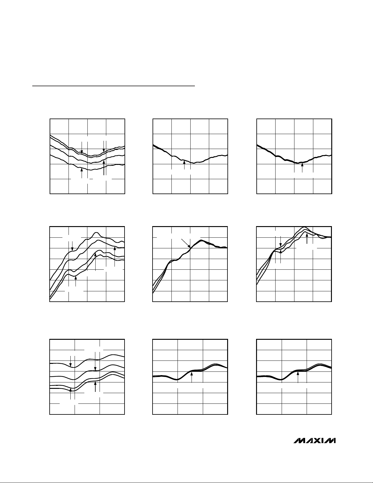
Typical Operating Characteristics
(MAX9984 Typical Application Circuit, using component values in Table 1, VCC= +5.0V, PLO= 0dBm, PRF= -5dBm, fRF> fLO, fIF=
160MHz, unless otherwise noted.)
6
7
9
8
10
11
700 800
900 1000
1100
CONVERSION GAIN vs. RF FREQUENCY
MAX9984 toc01
RF FREQUENCY (MHz)
CONVERSION GAIN (dB)
TC = +85°C
TC = -25°C
TC = -40°C
TC = +25°C
6
7
9
8
10
11
700 800
900 1000
1100
CONVERSION GAIN vs. RF FREQUENCY
MAX9984 toc02
RF FREQUENCY (MHz)
CONVERSION GAIN (dB)
PLO = -3dBm, 0dBm, +3dBm
6
7
9
8
10
11
700 800
900 1000
1100
CONVERSION GAIN vs. RF FREQUENCY
MAX9984 toc03
RF FREQUENCY (MHz)
CONVERSION GAIN (dB)
VCC = 4.75V, 5.0V, 5.25V
20
22
21
24
23
26
25
27
INPUT IP3 vs. RF FREQUENCY
MAX9984 toc04
RF FREQUENCY (MHz)
INPUT IP3 (dBm)
700 800 900 1000 1100
TC = +85°C
TC = -25°C
TC = -40°C
TC = +25°C
20
22
21
24
23
26
25
27
INPUT IP3 vs. RF FREQUENCY
MAX9984 toc05
RF FREQUENCY (MHz)
INPUT IP3 (dBm)
700 800 900 1000 1100
PLO = -3dBm, 0dBm, +3dBm
19
21
20
23
22
25
24
26
INPUT IP3 vs. RF FREQUENCY
MAX9984 toc06
RF FREQUENCY (MHz)
INPUT IP3 (dBm)
700 800 900 1000 1100
VCC = 5.25V
VCC = 5.0V
VCC = 4.75V
5
8
7
6
10
11
9
12
700 800 900 1000
NOISE FIGURE vs. RF FREQUENCY
MAX9984 toc07
RF FREQUENCY (MHz)
NOISE FIGURE (dB)
TC = -40°C
TC = +85°C
TC = +25°C
TC = -25°C
5
7
6
10
11
9
8
12
700 800 900 1000
NOISE FIGURE vs. RF FREQUENCY
MAX9984 toc08
RF FREQUENCY (MHz)
NOISE FIGURE (dB)
PLO = -3dBm, 0dBm, +3dBm
5
7
6
10
11
9
8
12
700 800 900 1000
NOISE FIGURE vs. RF FREQUENCY
MAX9984 toc09
RF FREQUENCY (MHz)
NOISE FIGURE (dB)
VCC = 4.75V, 5.0V, 5.25V
MAX9984
SiGe High-Linearity, 400MHz to 1000MHz
Downconversion Mixer with LO Buffer/Switch
4 _______________________________________________________________________________________
45
60
70
50
55
65
75
700 800 900 1000 1100
2RF-2LO RESPONSE vs. RF FREQUENCY
MAX9984 toc10
RF FREQUENCY (MHz)
2RF-2LO RESPONSE (dBc)
PRF = -5dBm
TC = -25°C, -40°C
TC = +85°C
TC = +25°C
45
60
70
50
55
65
75
700 800 900 1000 1100
2RF-2LO RESPONSE vs. RF FREQUENCY
MAX9984 toc11
RF FREQUENCY (MHz)
2RF-2LO RESPONSE (dBc)
PRF = -5dBm
PLO = -3dBm
PLO = 0dBm
PLO = +3dBm
45
60
75
70
50
55
65
80
700 800 900 1000 1100
2RF-2LO RESPONSE vs. RF FREQUENCY
MAX9984 toc12
RF FREQUENCY (MHz)
2RF-2LO RESPONSE (dBc)
PRF = -5dBm
VCC = 5.25V
VCC = 5.0V
VCC = 4.75V
55
65
75
85
95
700 800 900 1000 1100
3RF-3LO RESPONSE vs. RF FREQUENCY
MAX9984 toc13
RF FREQUENCY (MHz)
3RF-3LO RESPONSE (dBc)
PRF = -5dBm
TC = -25°C
TC = -40°C
TC = +85°C
TC = +25°C
55
65
75
85
95
700 800 900 1000 1100
3RF-3LO RESPONSE vs. RF FREQUENCY
MAX9984 toc14
RF FREQUENCY (MHz)
3RF-3LO RESPONSE (dBc)
PRF = -5dBm
PLO = -3dBm, 0dBm, +3dBm
55
65
75
85
95
700 800 900 1000 1100
3RF-3LO RESPONSE vs. RF FREQUENCY
MAX9984 toc15
RF FREQUENCY (MHz)
3RF-3LO RESPONSE (dBc)
PRF = -5dBm
VCC = 5.25V
VCC = 5.0V
VCC = 4.75V
9
12
14
11
10
13
15
700 800 900 1000 1100
INPUT P
1dB
vs. RF FREQUENCY
MAX9984 toc16
RF FREQUENCY (MHz)
INPUT P
1dB
(dBm)
TC = -40°C
TC = +85°C
TC = +25°C
TC = -25°C
9
12
14
11
10
13
15
700 800 900 1000 1100
INPUT P
1dB
vs. RF FREQUENCY
MAX9984 toc17
RF FREQUENCY (MHz)
INPUT P
1dB
(dBm)
PLO = -3dBm, 0dBm, +3dBm
9
12
14
11
10
13
15
700 800 900 1000 1100
INPUT P
1dB
vs. RF FREQUENCY
MAX9984 toc18
RF FREQUENCY (MHz)
INPUT P
1dB
(dBm)
VCC = 4.75V
VCC = 5.0V
VCC = 5.25V
Typical Operating Characteristics (continued)
(MAX9984 Typical Application Circuit, using component values in Table 1, VCC= +5.0V, PLO= 0dBm, PRF= -5dBm, fRF> fLO, fIF=
160MHz, unless otherwise noted.)
MAX9984
SiGe High-Linearity, 400MHz to 1000MHz
Downconversion Mixer with LO Buffer/Switch
_______________________________________________________________________________________ 5

Typical Operating Characteristics (continued)
(MAX9984 Typical Application Circuit, using component values in Table 1, VCC= +5.0V, PLO= 0dBm, PRF= -5dBm, fRF> fLO, fIF=
160MHz, unless otherwise noted.)
40
45
55
50
60
540 640 740 840 940
LO SWITCH ISOLATION
vs. LO FREQUENCY
MAX9984 toc20
LO FREQUENCY (MHz)
LO SWITCH ISOLATION (dB)
PLO = -3dBm, 0dBm, +3dBm
40
45
55
50
60
540 640 740 840 940
LO SWITCH ISOLATION
vs. LO FREQUENCY
MAX9984 toc19
LO FREQUENCY (MHz)
LO SWITCH ISOLATION (dB)
TC = -25°C, -40°C
TC = +25°C
TC = +85°C
40
45
55
50
60
540 640 740 840 940
LO SWITCH ISOLATION
vs. LO FREQUENCY
MAX9984 toc21
LO FREQUENCY (MHz)
LO SWITCH ISOLATION (dB)
VCC = 4.75V, 5.0V, 5.25V
-40
-35
-20
-25
-30
-10
-15
540 640 740 840 940
LO LEAKAGE AT IF PORT
vs. LO FREQUENCY
MAX9984 toc22
LO FREQUENCY (MHz)
LO LEAKAGE (dBm)
TC = -25°C, -40°C
TC = +25°C
TC = +85°C
-40
-35
-20
-25
-30
-10
-15
540 640 740 840 940
LO LEAKAGE AT IF PORT
vs. LO FREQUENCY
MAX9984 toc23
LO FREQUENCY (MHz)
LO LEAKAGE (dBm)
PLO = -3dBm
PLO = 0dBm, +3dBm
-40
-35
-20
-25
-30
-10
-15
540 640 740 840 940
LO LEAKAGE AT IF PORT
vs. LO FREQUENCY
MAX9984 toc24
LO FREQUENCY (MHz)
LO LEAKAGE (dBm)
VCC = 4.75V
VCC = 5.25V
VCC = 5.0V
-50
-40
-30
-10
-20
540 640 740 840 940
LO LEAKAGE AT RF PORT
vs. LO FREQUENCY
MAX9984 toc25
LO FREQUENCY (MHz)
LO LEAKAGE AT RF PORT (dBm)
TC = -25°C, -40°C
TC = +85°C
TC = +25°C
-50
-40
-30
-10
-20
540 640 740 840 940
LO LEAKAGE AT RF PORT
vs. LO FREQUENCY
MAX9984 toc26
LO FREQUENCY (MHz)
LO LEAKAGE AT RF PORT (dBm)
PLO = -3dBm, 0dBm, +3dBm
-50
-40
-30
-10
-20
540 640 740 840 940
LO LEAKAGE AT RF PORT
vs. LO FREQUENCY
MAX9984 toc27
LO FREQUENCY (MHz)
LO LEAKAGE AT RF PORT (dBm)
VCC = 4.75V, 5.0V, 5.25V
MAX9984
SiGe High-Linearity, 400MHz to 1000MHz
Downconversion Mixer with LO Buffer/Switch
6 _______________________________________________________________________________________

RF-TO-IF ISOLATION
vs. RF FREQUENCY
MAX9984 toc28
RF FREQUENCY (MHz)
RF-TO-IF ISOLATION (dB)
1000900800
35
40
45
50
55
60
30
700 1100
TC = +85°C TC = -25°C
TC = -40°C
TC = +25°C
RF-TO-IF ISOLATION
vs. RF FREQUENCY
MAX9984 toc29
RF FREQUENCY (MHz)
RF-TO-IF ISOLATION (dB)
1000900800
35
40
45
50
55
60
30
700 1100
PLO = -3dBm, 0dBm, +3dBm
RF-TO-IF ISOLATION
vs. RF FREQUENCY
MAX9984 toc30
RF FREQUENCY (MHz)
RF-TO-IF ISOLATION (dB)
1000900800
35
40
45
50
55
60
30
700 1100
VCC = 5.25V
VCC = 5.0V
VCC = 4.75V
RF PORT RETURN LOSS
vs. RF FREQUENCY
MAX9984 toc31
RF FREQUENCY (MHz)
RF PORT RETURN LOSS (dB)
1000900800
25
20
15
10
5
0
30
700 1100
PLO = -3dBm, 0dBm, +3dBm
IF PORT RETURN LOSS
vs. IF FREQUENCY
MAX9984 toc32
IF FREQUENCY (MHz)
IF PORT RETURN LOSS (dB)
200100 150 250 300
25
20
15
10
5
0
30
50 350
VCC = 4.75V, 5.0V, 5.25V
40
0
50
30
20
10
540 640 840740 940
LO SELECTED RETURN LOSS
vs. LO FREQUENCY
MAX9984 toc33
LO FREQUENCY (MHz)
LO SELECTED RETURN LOSS (dB)
PLO = -3dBm
PLO = 0dBm
PLO = +3dBm
Typical Operating Characteristics (continued)
(MAX9984 Typical Application Circuit, using component values in Table 1, VCC= +5.0V, PLO= 0dBm, PRF= -5dBm, fRF> fLO, fIF=
160MHz, unless otherwise noted.)
MAX9984
SiGe High-Linearity, 400MHz to 1000MHz
Downconversion Mixer with LO Buffer/Switch
_______________________________________________________________________________________ 7
LO UNSELECTED RETURN LOSS
vs. LO FREQUENCY
0
5
10
15
20
LO UNSELECTED RETURN LOSS (dB)
25
30
PLO = -3dBm, 0dBm, +3dBm
540 640 840740 940
LO FREQUENCY (MHz)
240
MAX9984 toc34
230
220
SUPPLY CURRENT (mA)
210
200
-40 -15 10 35 8560
SUPPLY CURRENT
vs. TEMPERATURE (T
VCC = 5.25V
VCC = 4.75V
TEMPERATURE (°C)
)
C
VCC = 5.0V
MAX9984 toc35

MAX9984
SiGe High-Linearity, 400MHz to 1000MHz
Downconversion Mixer with LO Buffer/Switch
8 _______________________________________________________________________________________
Typical Operating Characteristics
(MAX9984 Typical Application Circuit, using component values in Table 2, VCC= +5.0V, PLO= 0dBm, PRF= -5dBm, fIF= 75MHz,
unless otherwise noted.)
70
65
60
55
50
45
400 440420 460 480 500
2RF-2LO RESPONSE vs. RF FREQUENCY
(TUNED FOR 400MHz TO 500MHz RF FREQUENCY)
MAX9984 toc38
RF FREQUENCY (MHz)
2RF-2LO RESPONSE (dBc)
LOW-SIDE INJECTION,
f
RF
> f
LO
PRF = -5dBm
TC = +85°C
TC = +25°C
TC = -25°C, -40°C
26
25
24
23
22
21
20
19
400 440420 460 480 500
INPUT IP3 vs. RF FREQUENCY
(TUNED FOR 400MHz TO 500MHz RF FREQUENCY)
MAX9984 toc37
RF FREQUENCY (MHz)
INPUT IP3 (dBm)
LOW-SIDE INJECTION, fRF > f
LO
TC = +85°C
TC = -25°C
TC = +25°C
TC = -40°C
75
65
55
45
35
400 440420 460 480 500
3RF-3LO RESPONSE vs. RF FREQUENCY
(TUNED FOR 400MHz TO 500MHz RF FREQUENCY)
MAX9984 toc39
RF FREQUENCY (MHz)
3RF-3LO RESPONSE (dBc)
TC = +85°C
TC = +25°C
TC = -25°C, -40°C
LOW-SIDE INJECTION, fRF > f
LO
PRF = -5dBm
0
5
10
15
20
25
30
400 440420 460 480 500
RF PORT RETURN LOSS vs. RF FREQUENCY
(TUNED FOR 400MHz TO 500MHz RF FREQUENCY)
MAX9984 toc40
RF FREQUENCY (MHz)
RF PORT RETURN LOSS (dB)
VCC = 5.0V, PLO = 0dBm, TC = +25°C
LOW-SIDE INJECTION, f
RF
> f
LO
40
30
20
10
0
50 100 150 200
IF PORT RETURN LOSS vs. IF FREQUENCY
(TUNED FOR 400MHz TO 500MHz RF FREQUENCY)
MAX9984 toc41
IF FREQUENCY (MHz)
IF PORT RETURN LOSS (dB)
VCC = 5.0V, PLO = 0dBm, TC = +25°C
LOW-SIDE INJECTION, f
RF
> f
LO
0
5
10
15
20
25
30
325 365345 385 405 425
LO SELECTED RETURN LOSS vs. LO FREQUENCY
(TUNED FOR 400MHz TO 500MHz RF FREQUENCY)
MAX9984 toc42
LO FREQUENCY (MHz)
LO SELECTED RETURN LOSS (dB)
VCC = 5.0V, PLO = 0dBm, TC = +25°C
LOW-SIDE INJECTION, f
RF
> f
LO
0
5
10
15
20
25
30
325 365345 385 405 425
LO UNSELECTED RETURN LOSS vs. LO FREQUENCY
(TUNED FOR 400MHz TO 500MHz RF FREQUENCY)
MAX9984 toc43
LO FREQUENCY (MHz)
LO UNSELECTED RETURN LOSS (dB)
VCC = 5.0V, PLO = 0dBm, TC = +25°C
LOW-SIDE INJECTION, f
RF
> f
LO
10
9
8
7
6
5
400 440420 460 480 500
CONVERSION GAIN vs. RF FREQUENCY
(TUNED FOR 400MHz TO 500MHz RF FREQUENCY)
MAX9984 toc44
RF FREQUENCY (MHz)
CONVERSION GAIN (dB)
HIGH-SIDE INJECTION, fLO > f
RF
TC = +85°C
TC = -40°C
TC = +25°C
TC = -25°C
10
9
8
7
6
5
400 440420 460 480 500
CONVERSION GAIN vs. RF FREQUENCY
(TUNED FOR 400MHz TO 500MHz RF FREQUENCY)
MAX9984 toc36
RF FREQUENCY (MHz)
CONVERSION GAIN (dB)
LOW-SIDE INJECTION, fRF > f
LO
TC = +85°C
TC = -40°C
TC = +25°C
TC = -25°C

MAX9984
SiGe High-Linearity, 400MHz to 1000MHz
Downconversion Mixer with LO Buffer/Switch
_______________________________________________________________________________________ 9
Typical Operating Characteristics (continued)
(MAX9984 Typical Application Circuit, using component values in Table 2, VCC= +5.0V, PLO= 0dBm, PRF= -5dBm, fIF= 75MHz,
unless otherwise noted.)
25
24
23
22
21
20
19
18
400 440420 460 480 500
INPUT IP3 vs. RF FREQUENCY
(TUNED FOR 400MHz TO 500MHz RF FREQUENCY)
MAX9984 toc45
RF FREQUENCY (MHz)
INPUT IP3 (dBm)
HIGH-SIDE INJECTION, fLO > f
RF
TC = -40°C
TC = +85°C
TC = +25°C
TC = -25°C
2LO-2RF RESPONSE vs. RF FREQUENCY
(TUNED FOR 400MHz TO 500MHz RF FREQUENCY)
80
HIGH-SIDE INJECTION, fLO > f
PRF = -5dBm
75
TC = +25°C, +85°C
70
TC = -25°C
RF
MAX9984 toc46
3LO-3RF RESPONSE vs. RF FREQUENCY
(TUNED FOR 400MHz TO 500MHz RF FREQUENCY)
75
HIGH-SIDE INJECTION, fLO > f
PRF = -5dBm
TC = +85°C
65
TC = +25°C
RF
TC = -25°C
MAX9984 toc47
RF PORT RETURN LOSS vs. RF FREQUENCY
(TUNED FOR 400MHz TO 500MHz RF FREQUENCY)
0
VCC = 5.0V, PLO = 0dBm, TC = +25°C
HIGH-SIDE INJECTION, f
5
10
15
20
RF PORT RETURN LOSS (dB)
25
30
400 440420 460 480 500
RF FREQUENCY (MHz)
> f
RF
LO
MAX9984 toc48
65
60
2LO-2RF RESPONSE (dBc)
55
50
TC = -40°C
400 440420 460 480 500
RF FREQUENCY (MHz)
IF PORT RETURN LOSS vs. IF FREQUENCY
(TUNED FOR 400MHz TO 500MHz RF FREQUENCY)
0
VCC = 5.0V, PLO = 0dBm, TC = +25°C
HIGH-SIDE INJECTION, f
10
20
IF PORT RETURN LOSS (dB)
30
40
50 100 150 200
IF FREQUENCY (MHz)
> f
LO
RF
MAX9984 toc49
LO UNSELECTED RETURN LOSS vs. LO FREQUENCY
(TUNED FOR 400MHz TO 500MHz RF FREQUENCY)
0
VCC = 5.0V, PLO = 0dBm, TC = +25°C
HIGH-SIDE INJECTION, f
5
> f
LO
RF
MAX9984 toc51
55
TC = -40°C
45
3LO-3RF RESPONSE (dBc)
35
400 440420 460 480 500
RF FREQUENCY (MHz)
LO SELECTED RETURN LOSS vs. LO FREQUENCY
(TUNED FOR 400MHz TO 500MHz RF FREQUENCY)
0
VCC = 5.0V, PLO = 0dBm, TC = +25°C
HIGH-SIDE INJECTION, f
5
10
15
20
LO SELECTED RETURN LOSS (dB)
25
30
475 515495 535 555 575
LO FREQUENCY (MHz)
> f
LO
RF
MAX9984 toc50
10
15
20
25
LO UNSELECTED RETURN LOSS (dB)
30
475 515495 535 555 575
LO FREQUENCY (MHz)

MAX9984
SiGe High-Linearity, 400MHz to 1000MHz
Downconversion Mixer with LO Buffer/Switch
10 ______________________________________________________________________________________
Detailed Description
The MAX9984 high-linearity downconversion mixer
provides 8.1dB of conversion gain and +25dBm of
IIP3, with a typical 9.3dB noise figure. The integrated
baluns and matching circuitry allow for 50Ω singleended interfaces to the RF and the two LO ports. A single-pole, double-throw (SPDT) switch provides 50ns
switching time between the two LO inputs with 54dB of
LO-to-LO isolation. Furthermore, the integrated LO
buffer provides a high drive level to the mixer core,
reducing the LO drive required at the MAX9984’s
inputs to a -3dBm to +3dBm range. The IF port incorporates a differential output, which is ideal for providing enhanced IIP2 performance.
Specifications are guaranteed over broad frequency
ranges to allow for use in cellular band GSM,
cdma2000, iDEN, and W-CDMA 2G/2.5G/3G base stations. The MAX9984 is optimized to operate over a
815MHz to 1000MHz RF frequency range, a 570MHz to
850MHz LO frequency range, and a 50MHz to 250MHz
IF frequency range. Operation beyond these ranges is
possible; see the Typical Operating Characteristics for
additional details. For operation at a 400MHz to
500MHz RF frequency range, see the Typical
Operating Characteristics and Table 2 for details.
RF Input and Balun
The MAX9984 RF input is internally matched to 50Ω,
requiring no external matching components. A DCblocking capacitor is required because the input is internally DC shorted to ground through the on-chip balun.
LO Inputs, Buffer, and Balun
The MAX9984 is ideally suited for low-side LO injection
applications with an optimized 570MHz to 850MHz LO
frequency range. Appropriate tuning allows for an LO
frequency range below 570MHz (RF frequency below
815MHz). For a device with a 960MHz to 1180MHz LO
frequency range, refer to the MAX9986 data sheet. As
an added feature, the MAX9984 includes an internal LO
SPDT switch that can be used for frequency-hopping
applications. The switch selects one of the two singleended LO ports, allowing the external oscillator to settle
on a particular frequency before it is switched in. LO
switching time is typically less than 50ns, which is more
than adequate for virtually all GSM applications. If frequency hopping is not employed, set the switch to
either of the LO inputs. The switch is controlled by a
digital input (LOSEL): logic-high selects LO2, logic-low
selects LO1. To avoid damage to the part, voltage must
be applied to VCCbefore digital logic is applied to
LOSEL. LO1 and LO2 inputs are internally matched to
50Ω, requiring only a 82pF DC-blocking capacitor.
Pin Description
PIN NAME FUNCTION
1, 6, 8, 14 V
2RF
3 TAP
4, 5, 10, 12,
13, 17
7 LOBIAS Bias Resistor for Internal LO Buffer. Connect a 619Ω ±1% resistor from LOBIAS to the power supply.
9 LOSEL Local Oscillator Select. Logic control input for selecting LO1 or LO2.
11 LO1 Local Oscillator Input 1. Drive LOSEL low to select LO1.
15 LO2 Local Oscillator Input 2. Drive LOSEL high to select LO2.
16 LEXT
18, 19 IF-, IF+
20 IFBIAS IF Bias Resistor Connection for IF Amplifier. Connect a 953Ω ±1% resistor from IFBIAS to GND.
EP GND Exposed Ground Paddle. Solder the exposed paddle to the ground plane using multiple vias.
CC
GND Ground
Power-Supply Connection. Bypass each VCC pin to GND with capacitors as shown in the Typical
Application Circuit.
Single-Ended 50Ω RF Input. This port is internally matched and DC shorted to GND through a balun.
Requires an external DC-blocking capacitor.
Center Tap of the Internal RF Balun. Bypass to GND with capacitors close to the IC, as shown in the
Typical Application Circuit.
External Inductor Connection. Connect a low-ESR, 47nH inductor from LEXT to GND. This inductor
carries approximately 140mA DC current.
Differential IF Outputs. Each output requires external bias to V
Typical Application Circuit).
through an RF choke (see the
CC

MAX9984
SiGe High-Linearity, 400MHz to 1000MHz
Downconversion Mixer with LO Buffer/Switch
______________________________________________________________________________________ 11
A two-stage internal LO buffer allows a wide input
power range for the LO drive. All guaranteed specifications are for an LO signal power from -3dBm to +3dBm.
The on-chip low-loss balun, along with an LO buffer,
drives the double-balanced mixer. All interfacing and
matching components from the LO inputs to the IF outputs are integrated on-chip.
High-Linearity Mixer
The core of the MAX9984 is a double-balanced, highperformance passive mixer. Exceptional linearity is provided by the large LO swing from the on-chip LO
buffer. When combined with the integrated IF amplifiers, the cascaded IIP3, 2RF-2LO rejection, and NF
performance is typically 25dBm, 71dBc, and 9.3dB,
respectively.
Differential IF Output Amplifier
The MAX9984 mixer has a 50MHz to 250MHz IF frequency range. The differential, open-collector IF output
ports require external pullup inductors to VCC. Note that
these differential outputs are ideal for providing
enhanced 2RF-2LO rejection performance. Singleended IF applications require a 4:1 balun to transform
the 200Ω differential output impedance to a 50Ω singleended output.
Applications Information
Input and Output Matching
The RF and LO inputs are internally matched to 50Ω. No
matching components are required for an 815MHz to
1000MHz RF frequency range. RF and LO inputs
require only DC-blocking capacitors for interfacing.
The IF output impedance is 200Ω (differential). For
evaluation, an external low-loss 4:1 (impedance ratio)
balun transforms this impedance down to a 50Ω singleended output (see the Typical Application Circuit).
Capacitor CPis used at the RF input port to tune the
mixer down to operate in the 400MHz to 500MHz RF
frequency range (see Table 2). Operation between
500MHz to 815MHz would require a smaller capacitor
CP. Contact the factory for details.
Bias Resistors
Bias currents for the LO buffer and the IF amplifier are
optimized by fine tuning resistors R1 and R2. If
reduced current is required at the expense of performance, contact the factory for details. If the ±1% bias
resistor values are not readily available, substitute standard ±5% values.
LEXT Inductor
LEXT serves to improve the LO-to-IF and RF-to-IF leakage. The inductance value can be adjusted by the user to
optimize the performance for a particular frequency
band. Since approximately 140mA flows through this
inductor, it is important to use a low-DCR wire-wound coil.
If the LO-to-IF and RF-to-IF leakage are not critical
parameters, the inductor can be replaced by a short
circuit to ground.
Layout Considerations
A properly designed PC board is an essential part of
any RF/microwave circuit. Keep RF signal lines as short
as possible to reduce losses, radiation, and inductance. For the best performance, route the ground pin
traces directly to the exposed pad under the package.
The PC board exposed pad MUST be connected to the
ground plane of the PC board. It is suggested that multiple vias be used to connect this pad to the lower-level
ground planes. This method provides a good RF/thermal conduction path for the device. Solder the exposed
pad on the bottom of the device package to the PC
board. The MAX9984 evaluation kit can be used as a
reference for board layout. Gerber files are available
upon request at www.maxim-ic.com.
Power-Supply Bypassing
Proper voltage-supply bypassing is essential for highfrequency circuit stability. Bypass each VCCpin and
TAP with the capacitors shown in the Typical Application
Circuit; see Table 1. Place the TAP bypass capacitor to
ground within 100 mils of the TAP pin.
Exposed Pad RF/Thermal Considerations
The exposed paddle (EP) of the MAX9984’s 20-pin thin
QFN-EP package provides a low thermal-resistance
path to the die. It is important that the PC board on
which the MAX9984 is mounted be designed to conduct heat from the EP. In addition, provide the EP with
a low-inductance path to electrical ground. The EP
MUST be soldered to a ground plane on the PC board,
either directly or through an array of plated via holes.
Chip Information
TRANSISTOR COUNT: 1017
PROCESS: SiGe BiCMOS

MAX9984
SiGe High-Linearity, 400MHz to 1000MHz
Downconversion Mixer with LO Buffer/Switch
12 ______________________________________________________________________________________
Table 1. Component List Referring to the Typical Application Circuit for 815MHz to
1000MHz RF Frequency Operation
Table 2. Component List Referring to the Typical Application Circuit for 400MHz to
995MHz RF Frequency Operation
C2, C4, C7, C8, C10, C11, C12 82pF Microwave capacitors (0603)
COMPONENT VALUE DESCRIPTION
L1, L2 330nH Wire-wound high-Q inductors (0805)
L3 47nH Wire-wound high-Q inductor (0603)
C1 10pF Microwave capacitor (0603)
C3, C5, C6, C9, C13, C14 0.01µF Microwave capacitors (0603)
C15 220pF Microwave capacitor (0402)
R1 953Ω±1% resistor (0603)
R2 619Ω±1% resistor (0603)
R3 3.57Ω±1% resistor (1206)
T1 4:1 balun IF balun (TC4-1W-7A)
U1 MAX9984 Maxim IC
COMPONENT VALUE DESCRIPTION
L1, L2 820nH Wire-wound high-Q inductors (0805)
L3 47nH Wire-wound high-Q inductor (0603)
C
P
C1 56pF Microwave capacitor (0603)
C2, C4, C7, C8, C10,
C11, C12
C3, C5, C6, C9, C13, C14 10nF Microwave capacitors (0603)
C15 220pF Microwave capacitor (0402)
R1 953Ω±1% resistor (0603)
R2 619Ω±1% resistor (0603)
R3 3.57Ω±1% resistor (1206)
T1 4:1 balun IF balun (TC4-1W-7A)
U1 MAX9984 Maxim IC
7pF Microwave capacitor (0603)
220pF Microwave capacitors (0603)

MAX9984
SiGe High-Linearity, 400MHz to 1000MHz
Downconversion Mixer with LO Buffer/Switch
______________________________________________________________________________________ 13
Pin Configuration/Functional Diagram
MAX9984
1
2
3
4
5
15
14
13
12
11
6
7
8910
20
19
18
17
16
GND
LOSEL
LOBIAS
TAP
RF
V
CC
THIN QFN
V
CC
V
CC
V
CC
GND
GND
LO2
GND
LEXT
IFBIAS
IF-
IF+
GND
LO1
GND

MAX9984
SiGe High-Linearity, 400MHz to 1000MHz
Downconversion Mixer with LO Buffer/Switch
14 ______________________________________________________________________________________
Typical Application Circuit
V
CC
T1
R3
L1
326
IF
OUTPUT
RF
INPUT
CP*
R1
1
2
3
4
5
CC
C6 C7
L2
4
IFBIAS
20
6
CC
V
R2
IF+
19
7
LOBIAS
C15
GND
IF18
17 16
MAX9984
8
9
CC
V
LOSEL
LEXT
10
GND
1
L3
LOSEL
INPUT
LO2
15
V
14
GND
13
GND
12
LO1
11
C12
CC
C10
C11
LO2
INPUT
V
CC
LO1
INPUT
C13
C14
V
CC
C3
C2
C1
C5
C4
V
TAP
GND
GND
CC
RF
V
NEEDED FOR 400MHz TO 500MHz RF FREQUENCY OPERATION. SEE TABLE 2.
*C
P
C8
C9
V
CC

MAX9984
SiGe High-Linearity, 400MHz to 1000MHz
Downconversion Mixer with LO Buffer/Switch
Maxim cannot assume responsibility for use of any circuitry other than circuitry entirely embodied in a Maxim product. No circuit patent licenses are
implied. Maxim reserves the right to change the circuitry and specifications without notice at any time.
Maxim Integrated Products, 120 San Gabriel Drive, Sunnyvale, CA 94086 408-737-7600 ____________________ 15
© 2005 Maxim Integrated Products Printed USA is a registered trademark of Maxim Integrated Products, Inc.
Package Information
(The package drawing(s) in this data sheet may not reflect the most current specifications. For the latest package outline information
go to www.maxim-ic.com/packages
.)
C
D
XXXXX
D2
b
C
L
D/2
E/2
E
e
L1
0.10 C
A
0.08 C
A3
A1
(NE-1) X e
DETAIL A
L
D2/2
k
e
(ND-1) X e
L
e e
PACKAGE OUTLINE,
16, 20, 28, 32, 40L THIN QFN, 5x5x0.8mm
0.10 M C A B
H
LL
1
2
QFN THIN.EPS
L
E2/2
C
E2
L
DETAIL B
PIN # 1 I.D.
0.35x45°
CC
L
e/2
21-0140
MARKING
PIN # 1
I.D.
-DRAWING NOT TO SCALE-
PKG.
SYMBOL
A
A1
A3
b
D
E
e
k
L
L1
N
ND
NE
JEDEC
NOTES:
1. DIMENSIONING & TOLERANCING CONFORM TO ASME Y14.5M-1994.
2. ALL DIMENSIONS ARE IN MILLIMETERS. ANGLES ARE IN DEGREES.
3. N IS THE TOTAL NUMBER OF TERMINALS.
4. THE TERMINAL #1 IDENTIFIER AND TERMINAL NUMBERING CONVENTION SHALL
CONFORM TO JESD 95-1 SPP-012. DETAILS OF TERMINAL #1 IDENTIFIER ARE
OPTIONAL, BUT MUST BE LOCATED WITHIN THE ZONE INDICATED. THE TERMINAL #1
IDENTIFIER MAY BE EITHER A MOLD OR MARKED FEATURE.
5. DIMENSION b APPLIES TO METALLIZED TERMINAL AND IS MEASURED BETWEEN
0.25 mm AND 0.30 mm FROM TERMINAL TIP.
6. ND AND NE REFER TO THE NUMBER OF TERMINALS ON EACH D AND E SIDE RESPECTIVELY.
7. DEPOPULATION IS POSSIBLE IN A SYMMETRICAL FASHION.
8. COPLANARITY APPLIES TO THE EXPOSED HEAT SINK SLUG AS WELL AS THE TERMINALS.
9. DRAWING CONFORMS TO JEDEC MO220, EXCEPT EXPOSED PAD DIMENSION FOR T2855-1,
T2855-3, AND T2855-6.
10. WARPAGE SHALL NOT EXCEED 0.10 mm.
11. MARKING IS FOR PACKAGE ORIENTATION REFERENCE ONLY.
12. NUMBER OF LEADS SHOWN ARE FOR REFERENCE ONLY.
13. LEAD CENTERLINES TO BE AT TRUE POSITION AS DEFINED BY BASIC DIMENSION "e", ±0.05.
-DRAWING NOT TO SCALE-
COMMON DIMENSIONS
16L 5x5
MIN. MAX.NOM.
0.70 0.800.75
0.05
0.02
0.20 REF.
0.25
0.350.30
5.10
5.00
4.90
5.105.00
4.90
0.80 BSC.
0.250--
0.30 0.500.40
---
16
4
4
WHHB
MIN.
0.70
0
0.25
4.90
4.90
0.25
0.45
---
20L 5x5
NOM.
0.75
0.02
0.20 REF.
0.30
5.00
5.00
0.65 BSC.
0.55
20
5
5
WHHC
28L 5x5
32L 5x5
MAX.
NOM.
MIN.
MAX.
0.70
0
0.20
4.90
4.90
0.25
0.45
0.75
0.02
0.20 REF.
0.25
5.00
5.00
0.50 BSC.
0.55
---
28
WHHD-1
7
7
0.80
0.70
0.05
0.30
5.10
5.10
--
0.65
MIN.
0
0.20 0.25 0.30
4.90
4.90
0.25
0.30
---
0.80
0.05
0.35
5.10
5.10
--
0.65
NOM.
0.75
0.02
0.20 REF.
5.00
5.00
0.50 BSC.
0.40
32
8
8
WHHD-2
MAX.
0.80
0.70
0.05
5.10
5.10
--
0.50
40L 5x5
MIN.
NOM.
0.75 0.80
0.20 REF.
0.15
4.90
5.00 5.10
4.90 5.00
0.40 BSC.
0.25 0.35 0.45
0.30
0.40 0.50
40
10
10
-----
MAX.
0.0500.02
0.250.20
5.10
0.600.40 0.50
EXPOSED PAD VARIATIONS
PKG.
CODES
T1655-1 3.203.00 3.10 3.00 3.10 3.20
T2855-2 2.60 2.602.80 2.70 2.80
T2855-3 3.15 3.25 3.35 3.15 3.25 3.35
T2855-4 2.60 2.70 2.80 2.60 2.70 2.80
T2855-5 2.60 2.70 2.80 2.60 2.70 2.80
T2855-6 3.15 3.25 3.35 3.15 3.25 3.35
T2855-7 2.60 2.70
T3255-2
D2
MAX.
NOM.MIN.
MIN.E2NOM. MAX.
3.203.00T1655-2 3.10 3.00 3.10 3.20 Y ES
3.20
3.00T2055-2 3.10
3.103.00 3.203.103.00 3.20T2055-4
3.353.15T2055-5 3.25 3.15 3.25 3.35
3.353.15T2855-1 3.25 3.353.15 3.25
2.70
2.80
2.60 2.70 2.80
3.35
3.15T2855-8 3.25 3.15 3.25 3.35
3.35
3.15T2855N-1 3.25 3.15 3.25 3.35
3.20
3.00
3.00 3.10 3.20
3.10
3.203.00 3.10T3255-3 3.203.00 3.10
3.203.00 3.10T3255-4 3.203.00 3.10
3.203.10T3255N-1 3.00
3.30T4055-1 3.20 3.40 3.20 3.30 3.40
SEE COMMON DIMENSIONS TABLE
**
PACKAGE OUTLINE,
16, 20, 28, 32, 40L THIN QFN, 5x5x0.8mm
21-0140
DOWN
L
BONDS
±0.15
ALLOWED
NO
**
**
NO3.203.103.003.10T1655N-1 3.00 3.20
**
**
3.203.00 3.10
NO
YES3.103.00 3.203.103.00 3.20T2055-3
**
NO
**
YES
0.40
NO
**
NO
**
YES
**
YES
**
NO
**
NO
**
YES
**
0.40
YES
NO
**
NO
**
YES
**
NO
**
NO
3.203.103.00
**
YES
**
2
H
2
 Loading...