

Page 1
General Description
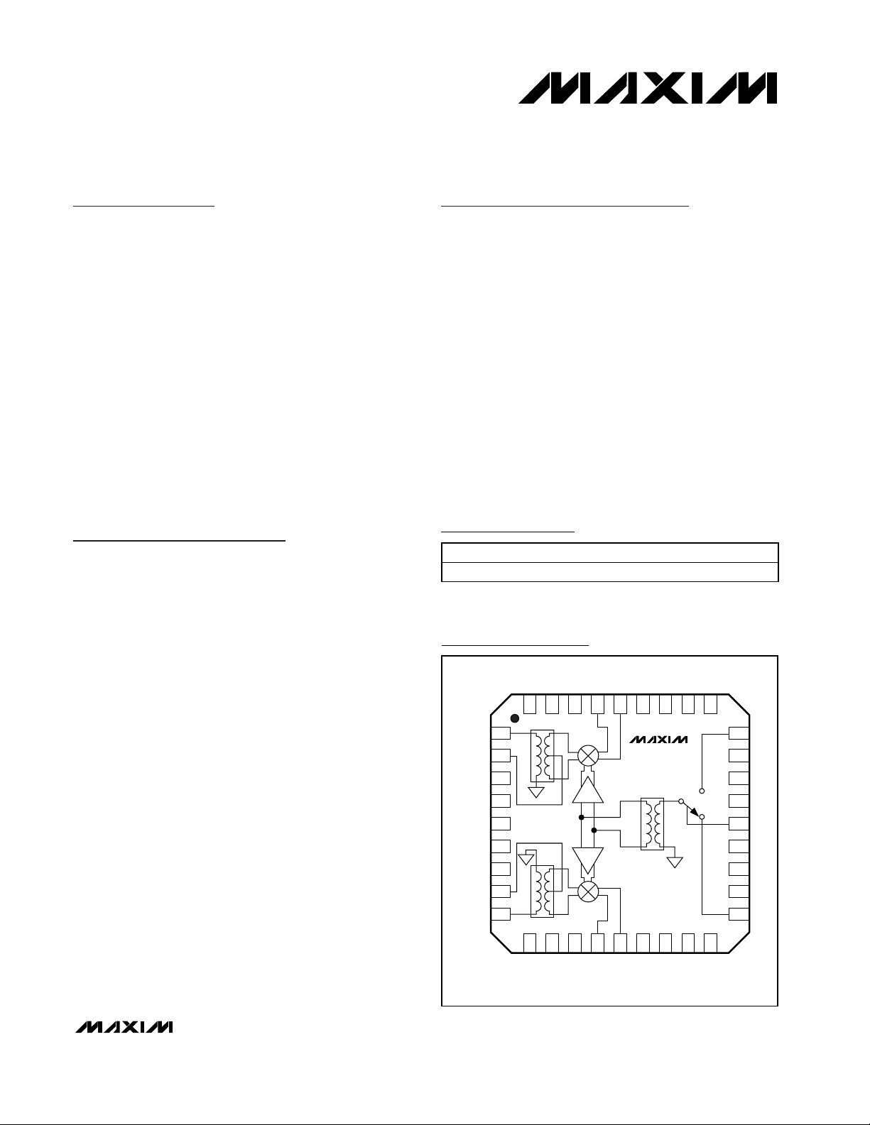
The MAX9981 dual high-linearity mixer integrates a local
oscillator (LO) switch, LO buffer, LO splitter, and two
active mixers. On-chip baluns allow for single-ended RF
and LO inputs. The active mixers eliminate the need for
an additional IF amplifier because the mixer provides a
typical overall conversion gain of 2.1dB.
The MAX9981 active mixers are optimized to meet the
demanding requirements of GSM850, GSM900, and
CDMA850 base-station receivers. These mixers provide
exceptional linearity with an input IP3 of greater than
+27dBm. The integrated LO driver allows for a wide
range of LO drive levels from -5dBm to +5dBm. In addition, the built-in high-isolation switch enables rapid LO
selection of less than 250ns, as needed for GSM transceiver designs.
The MAX9981 is available in a 36-pin QFN package
(6mm ✕ 6mm) with an exposed paddle, and is specified
over the -40°C to +85°C extended temperature range.
Applications
GSM850/GSM900 2G and 2.5G EDGE BaseStation Receivers
Cellular cdmaOne™ and cdma2000™ BaseStation Receivers
TDMA and Integrated Digital Enhanced Network
(iDEN)™ Base-Station Receivers
Digital and Spread-Spectrum Communication
Systems
Microwave Point-to-Point Links
Features
♦ +27.3dBm Input IP3
♦ +13.6dBm Input 1dB Compression Point
♦ 825MHz to 915MHz RF Frequency Range
♦ 70MHz to 170MHz IF Frequency Range
♦ 725MHz to 1085MHz LO Frequency Range
♦ 2.1dB Conversion Gain
♦ 10.8dB Noise Figure
♦ 42dB Channel-to-Channel Isolation
♦ -5dBm to +5dBm LO Drive
♦ +5V Single-Supply Operation
♦ Built-In LO Switch with 52dB LO1 to LO2 Isolation
♦ ESD Protection
♦ Integrated RF and LO Baluns for Single-Ended
Inputs
MAX9981
825MHz to 915MHz, Dual SiGe High-Linearity
Active Mixer
________________________________________________________________ Maxim Integrated Products 1
Ordering Information
19-2588; Rev 0; 9/02
For pricing, delivery, and ordering information, please contact Maxim/Dallas Direct! at
1-888-629-4642, or visit Maxim’s website at www.maxim-ic.com.
Pin Configuration/
Functional Diagram
*EP = Exposed paddle.
cdmaOne is a trademark of CDMA Development Group.
cdma2000 is a trademark of Telecommunications Industry
Association.
iDEN is a trademark of Motorola, Inc.
PART TEMP RANGE PIN-PACKAGE
MAX9981EGX-T -40°C to +85°C 36 QFN-EP* (6mm × 6mm)
TOP VIEW
RFMAIN
TAPMAIN
MAINBIAS
GND
GND
GND
DIVBIAS
TAPDIV
RFDIV
CC
V
36
1
2
3
4
5
6
7
8
9
10
CC
V
GND
31
MAX9981
15
GND
CC
GND
V
29
30
17
16
CC
V
GND
IFMAIN-
IFMAIN+
GND
GND
35
34
11
12
GND
GND
6mm x 6mm QFN-EP
33
13
IFDIV+
32
14
IFDIV-
GND
28
18
GND
27 LO2
26
GND
GND
25
24
GND
LOSEL
23
GND
22
V
21
GND
20
19
LO1
CC
Page 2
MAX9981
825MHz to 915MHz, Dual SiGe High-Linearity
Active Mixer
2 _______________________________________________________________________________________
ABSOLUTE MAXIMUM RATINGS
DC ELECTRICAL CHARACTERISTICS
(Typical Application Circuit, VCC= +4.75V to +5.25V, no RF signals applied, all RF inputs and outputs terminated with 50Ω,
267Ω resistors connected from MAINBIAS and DIVBIAS to GND, T
A
= -40°C to +85°C, unless otherwise noted. Typical values are at
V
CC
= +5.0V, TA= +25°C, unless otherwise noted.)
Stresses beyond those listed under “Absolute Maximum Ratings” may cause permanent damage to the device. These are stress ratings only, and functional
operation of the device at these or any other conditions beyond those indicated in the operational sections of the specifications is not implied. Exposure to
absolute maximum rating conditions for extended periods may affect device reliability.
VCC........................................................................-0.3V to +5.5V
IFMAIN+, IFMAIN-, IFDIV+, IFDIV-,
MAINBIAS, DIVBIAS, LOSEL..................-0.3V to (VCC+ 0.3V)
TAPMAIN, TAPDIV ..............................................................+5.5V
MAINBIAS, DIVBIAS Current ................................................5mA
RFMAIN, RFDIV, LO1, LO2 Input Power ........................+20dBm
Continuous Power Dissipation (TA= +70°C)
36-Pin QFN (derate 33mW/°C above +70°C)..............2200mW
Operating Temperature Range ...........................-40°C to +85°C
Junction Temperature......................................................+150°C
Storage Temperature Range .............................-65°C to +150°C
Lead Temperature (soldering, 10s) .................................+300°C
AC ELECTRICAL CHARACTERISTICS
(Typical Application Circuit, VCC= +4.75V to +5.25V, PLO= -5dBm to +5dBm, fRF= 825MHz to 915MHz, fLO= 725MHz to 1085MHz,
T
A
= -40°C to +85°C, unless otherwise noted. Typical values are at VCC= +5.0V, PRF= -5dBm, PLO= 0dBm, fRF= 870MHz,
f
LO
= 770MHz, TA= +25°C, unless otherwise noted.) (Notes 1, 2)
Supply Voltage V
Supply Current I
Input High Voltage V
Input Low Voltage V
LOSEL Input Current I
PARAMETER SYMBOL CONDITIONS MIN TYP MAX UNITS
CC
CC
IH
IL
LOSEL
4.75 5.00 5.25 V
260 291 325 mA
3.5 V
0.4 V
-5 +5 µA
RF Frequency f
LO Frequency f
IF Frequency f
LO Drive Level P
Conversion Gain (Note 3) G
Gain Variation from Nominal fRF = 825MHz to 915MHz, 3σ ±0.6 dB
Conversion Loss from LO to IF
Noise Figure NF
PARAMETER SYMBOL CONDITIONS MIN TYP MAX UNITS
RF
LO
IF
LO
Must meet RF and LO frequency range. IF
matching components affect IF frequency
range.
VCC = +5.0V,
f
= 100MHz,
IF
low-side injection,
C
P
= 0dBm,
RF
= -5dBm
P
LO
Inject P
LO port. Measure 100MHz at IF port as
P
100MHz IF,
low-side
injection
= -20dBm at fLO + 100MHz into
IN
. No RF signal at RF port.
OUT
Cellular band,
f
= 825MHz to 850MHz
RF
GSM band,
= 880MHz to 915MHz
f
RF
Cellular band,
f
= 825MHz to
RF
850MHz
GSM band,
= 880MHz
f
RF
to 915MHz
825 915 MHz
725 1085 MHz
70 170 MHz
-5 +5 dBm
2.7
dB
2.1
53 dB
10.8
dB
11.9
Page 3
MAX9981
825MHz to 915MHz, Dual SiGe High-Linearity
Active Mixer
_______________________________________________________________________________________ 3
Note 1: Guaranteed by design and characterization.
Note 2: All limits reflect losses of external components. Output measurements taken at IF OUT of Typical Application Circuit.
Note 3: Production tested.
Note 4: Two tones at 1MHz spacing, -5dBm per tone at RF port.
Note 5: Measured at IF port at IF frequency. f
LO1
and f
LO2
are offset by 1MHz.
Note 6: IF return loss can be optimized by external matching components.
AC ELECTRICAL CHARACTERISTICS (continued)
(Typical Application Circuit, VCC= +4.75V to +5.25V, PLO= -5dBm to +5dBm, fRF= 825MHz to 915MHz, fLO= 725MHz to 1085MHz,
T
A
= -40°C to +85°C, unless otherwise noted. Typical values are at VCC= +5.0V, PRF= -5dBm, PLO= 0dBm, fRF= 870MHz,
f
LO
= 770MHz, TA= +25°C, unless otherwise noted.) (Notes 1, 2)
Input 1dB Compression Point P
Input Third-Order Intercept Point IIP3 PLO = -5dBm to +5dBm (Notes 3, 4) 27.3 dBm
2 RF - 2 LO Spur Rejection 2 × 2
3 RF - 3 LO Spur Rejection 3 × 3
Maximum LO Leakage at RF Port
Maximum LO Leakage at IF Port
Minimum RF to IF Isolation
LO1 to LO2 Isolation
Minimum Channel Isolation
LO Switching Time 50% of LOSEL to IF settled within 2° 250 ns
RF Return Loss 25 dB
LO Return Loss
IF Return Loss
PARAMETER SYMBOL CONDITIONS MIN TYP MAX UNITS
1dB
Low-side injection 13.6 dBm
f
= 915MHz, fLO = 815MHz,
RF
= 865MHz, PRF = -5dBm
f
SPUR
f
= 915MHz, fLO = 815MHz,
RF
= 848.3MHz, PRF = -5dBm
f
SPUR
P
= -5dBm to +5dBm,
LO
f
= 725MHz to 1100MHz
LO
P
= -5dBm to +5dBm,
LO
f
= 725MHz to 1100MHz
LO
P
= -5dBm to +5dBm,
LO
f
= 825MHz to 915MHz
RF
f
= 825MHz to 915MHz, P
RF
+5dBm, f
= 825MHz
f
RF
to 915MHz,
f
LO
to 1085MHz
LO port selected 19
LO port unselected 14.3
RF and LO terminated into 50Ω,
= 100MHz (Note 6)
f
IF
= 100MHz (Note 5)
IF
= 725MHz
P
RFMAIN
terminated with 50Ω.
Measured power at IFDIV
relative to IFMAIN.
P
= -5dBm, RFMAIN
RFDIV
terminated with 50Ω.
Measured power at
IFMAIN relative to IFDIV.
Main 53.3
Diversity 43.2
= P
LO2
=
LO1
= -5dBm, RFDIV
dBc
79.7 dBc
-42 dBm
-30.6 dBm
18 dB
52 dB
39.5
dBc
42
dB
15 dB
Page 4
MAX9981
825MHz to 915MHz, Dual SiGe High-Linearity
Active Mixer
4 _______________________________________________________________________________________
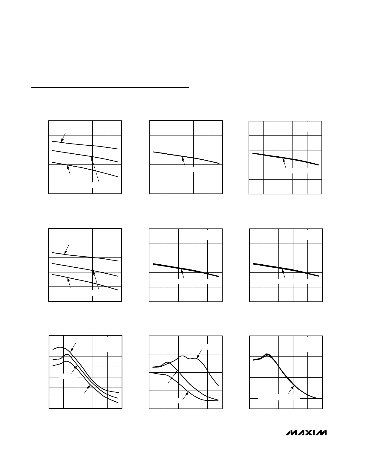
Typical Operating Characteristics
(Typical Application Circuit, VCC= 5.0V, PRF= -5dBm, PLO= 0dBm, TA= +25°C, unless otherwise noted.)
CONVERSION GAIN
vs. RF FREQUENCY LOW-SIDE INJECTION
MAX9981 toc01
RF FREQUENCY (MHz)
CONVERSION GAIN (dB)
900880860840
1
2
3
4
5
0
820 920
fIF = 100MHz
MAIN MIXER
TA = -40°C
TA = +85°C
TA = +25°C
CONVERSION GAIN
vs. RF FREQUENCY LOW-SIDE INJECTION
MAX9981 toc02
RF FREQUENCY (MHz)
CONVERSION GAIN (dB)
900880860840
1
2
3
4
5
0
820 920
fIF = 100MHz
MAIN MIXER
PLO = -5dBm, 0dBm, +5dBm
CONVERSION GAIN
vs. RF FREQUENCY LOW-SIDE INJECTION
MAX9981 toc03
RF FREQUENCY (MHz)
CONVERSION GAIN (dB)
900880860840
1
2
3
4
5
0
820 920
fIF = 100MHz
MAIN MIXER
VCC = 4.75V, 5.0V, 5.25V
CONVERSION GAIN
vs. RF FREQUENCY HIGH-SIDE INJECTION
MAX9981 toc04
RF FREQUENCY (MHz)
CONVERSION GAIN (dB)
900880860840
1
2
3
4
5
0
820 920
fIF = 120MHz
MAIN MIXER
TA = -40°C
TA = +85°C
TA = +25°C
CONVERSION GAIN
vs. RF FREQUENCY HIGH-SIDE INJECTION
MAX9981 toc05
RF FREQUENCY (MHz)
CONVERSION GAIN (dB)
900880860840
1
2
3
4
5
0
820 920
fIF = 120MHz
MAIN MIXER
PLO = -5dBm, 0dBm, +5dBm
CONVERSION GAIN
vs. RF FREQUENCY HIGH-SIDE INJECTION
MAX9981 toc06
RF FREQUENCY (MHz)
CONVERSION GAIN (dB)
900880860840
1
2
3
4
5
0
820 920
fIF = 120MHz
MAIN MIXER
VCC = 4.75V, 5.0V, 5.25V
2 RF - 2 LO RESPONSE
vs. RF FREQUENCY LOW-SIDE INJECTION
MAX9981 toc07
RF FREQUENCY (MHz)
2 RF - 2 LO RESPONSE (dBc)
900880860840
50
55
60
65
70
75
80
45
820 920
fIF = 100MHz
MAIN MIXER
P
RF
= -5dBm
TA = +85°C
TA = +25°C
TA = -40°C
2 RF - 2 LO RESPONSE
vs. RF FREQUENCY LOW-SIDE INJECTION
MAX9981 toc08
RF FREQUENCY (MHz)
2 RF - 2 LO RESPONSE (dBc)
900880860840
55
65
75
85
45
820 920
PLO = -5dBm
PLO = 0dBm
PLO = +5dBm
fIF = 100MHz
MAIN MIXER
P
RF
= -5dBm
2 RF - 2 LO RESPONSE
vs. RF FREQUENCY LOW-SIDE INJECTION
MAX9981 toc09
RF FREQUENCY (MHz)
2 RF - 2 LO RESPONSE (dBc)
900880860840
50
55
60
65
70
75
80
45
820 920
fIF = 100MHz
MAIN MIXER
P
RF
= -5dBm
VCC = 4.75V, 5.0V, 5.25V
Page 5
MAX9981
825MHz to 915MHz, Dual SiGe High-Linearity
Active Mixer
_______________________________________________________________________________________ 5
Typical Operating Characteristics (continued)
(Typical Application Circuit, VCC= 5.0V, PRF= -5dBm, PLO= 0dBm, TA= +25°C, unless otherwise noted.)
vs. RF FREQUENCY LOW-SIDE INJECTION
2 RF - 2 LO RESPONSE
60
TA = +85°C
55
50
45
2 RF - 2 LO RESPONSE (dBc)
40
820 920
TA = +25°C
RF FREQUENCY (MHz)
fIF = 100MHz
DIVERSITY MIXER
P
RF
TA = -40°C
2 LO - 2 RF RESPONSE
vs. RF FREQUENCY HIGH-SIDE INJECTION
70
65
60
55
2 LO - 2 RF RESPONSE (dBc)
50
45
820 920
RF FREQUENCY (MHz)
TA = +85°C
TA = +25°C
TA = -40°C
= -5dBm
900880860840
fIF = 120MHz
MAIN MIXER
= -5dBm
P
RF
900880860840
60
MAX9981 toc10
55
50
45
2 RF - 2 LO RESPONSE (dBc)
40
60
MAX9981 toc13
58
56
54
2 LO - 2 RF RESPONSE (dBc)
52
50
2 RF - 2 LO RESPONSE
vs. RF FREQUENCY LOW-SIDE INJECTION
fIF = 100MHz
PLO = -5dBm
DIVERSITY MIXER
= -5dBm
P
RF
900880860840
PLO = +5dBm
PLO = 0dBm
820 920
RF FREQUENCY (MHz)
2 LO - 2 RF RESPONSE
vs. RF FREQUENCY HIGH-SIDE INJECTION
fIF = 120MHz
MAIN MIXER
= -5dBm
P
RF
PLO = 0dBm
PLO = -5dBm
PLO = +5dBm
820 920
RF FREQUENCY (MHz)
900880860840
vs. RF FREQUENCY LOW-SIDE INJECTION
60
MAX9981 toc11
55
50
45
2 RF - 2 LO RESPONSE (dBc)
40
820 920
vs. RF FREQUENCY HIGH-SIDE INJECTION
60
MAX9981 toc14
58
56
54
2 LO - 2 RF RESPONSE (dBc)
52
50
820 920
VCC = 4.75V, 5.0V, 5.25V
2 RF - 2 LO RESPONSE
fIF = 100MHz
DIVERSITY MIXER
= -5dBm
P
RF
RF FREQUENCY (MHz)
2 LO - 2 RF RESPONSE
fIF = 120MHz
MAIN MIXER
P
VCC = 5.25V
VCC = 4.75, 5.0V
RF FREQUENCY (MHz)
900880860840
= -5dBm
RF
900880860840
MAX9981 toc12
MAX9981 toc15
vs. RF FREQUENCY HIGH-SIDE INJECTION
2 LO - 2 RF RESPONSE
47
46
45
TA = +85°C
44
43
42
2 LO - 2 RF RESPONSE (dBc)
41
40
TA = +25°C
TA = -40°C
820 920
RF FREQUENCY (MHz)
fIF = 120MHz
DIVERSITY MIXER
P
RF
= -5dBm
900880860840
vs. RF FREQUENCY HIGH-SIDE INJECTION
52.5
50.0
MAX9981 toc16
47.5
45.0
42.5
2 LO - 2 RF RESPONSE (dBc)
40.0
37.5
820 920
2 LO - 2 RF RESPONSE
PLO = 0dBm
PLO = +5dBm
RF FREQUENCY (MHz)
fIF = 120MHz
DIVERSITY MIXER
= -5dBm
P
RF
PLO = -5dBm
900880860840
vs. RF FREQUENCY HIGH-SIDE INJECTION
46
MAX9981 toc17
45
44
43
2 LO - 2 RF RESPONSE (dBc)
42
820 920
2 LO - 2 RF RESPONSE
VCC = 5.25V
VCC = 4.75V, 5.0V
RF FREQUENCY (MHz)
fIF = 120MHz
DIVERSITY MIXER
= -5dBm
P
RF
900880860840
MAX9981 toc18
Page 6

MAX9981
825MHz to 915MHz, Dual SiGe High-Linearity
Active Mixer
6 _______________________________________________________________________________________
Typical Operating Characteristics (continued)
(Typical Application Circuit, VCC= 5.0V, PRF= -5dBm, PLO= 0dBm, TA= +25°C, unless otherwise noted.)
vs. RF FREQUENCY LOW-SIDE INJECTION
30
29
TA = +85°C
28
INPUT IP3
fIF = 100MHz
MAIN MIXER
MAX9981 toc19
vs. RF FREQUENCY LOW-SIDE INJECTION
30
29
28
INPUT IP3
PLO = +5dBm
fIF = 100MHz
MAIN MIXER
MAX9981 toc20
vs. RF FREQUENCY LOW-SIDE INJECTION
INPUT IP3
30
29
VCC = 5.25V
28
fIF = 100MHz
MAIN MIXER
MAX9981 toc21
27
INPUT IP3 (dBm)
26
25
TA = +25°C
TA = -40°C
820 920
RF FREQUENCY (MHz)
INPUT IP3
vs. RF FREQUENCY HIGH-SIDE INJECTION
30
29
28
27
INPUT IP3 (dBm)
TA = +25°C
26
25
820 920
RF FREQUENCY (MHz)
TA = -40°C
TA = +85°C
INPUT P1dB
vs. RF FREQUENCY LOW-SIDE INJECTION
17
16
900880860840
fIF = 120MHz
MAIN MIXER
900880860840
fIF = 100MHz
MAIN MIXER
MAX9981 toc22
MAX9981 toc25
27
INPUT IP3 (dBm)
26
25
PLO = 0dBm
PLO = -5dBm
820 920
RF FREQUENCY (MHz)
INPUT IP3
vs. RF FREQUENCY HIGH-SIDE INJECTION
30
29
28
27
INPUT IP3 (dBm)
PLO = 0dBm
26
25
820 920
PLO = -5dBm
PLO = +5dBm
RF FREQUENCY (MHz)
INPUT P1dB
vs. RF FREQUENCY LOW-SIDE INJECTION
17
16
900880860840
fIF = 120MHz
MAIN MIXER
900880860840
fIF = 100MHz
MAIN MIXER
MAX9981 toc23
MAX9981 toc26
27
INPUT IP3 (dBm)
26
VCC = 4.75V
25
820 920
VCC = 5.0V
RF FREQUENCY (MHz)
INPUT IP3
vs. RF FREQUENCY HIGH-SIDE INJECTION
30
29
28
27
INPUT IP3 (dBm)
26
25
820 920
VCC = 5.25V
VCC = 5.0V
VCC = 4.75V
RF FREQUENCY (MHz)
INPUT P1dB
vs. RF FREQUENCY LOW-SIDE INJECTION
17
16
900880860840
fIF = 120MHz
MAIN MIXER
900880860840
fIF = 100MHz
MAIN MIXER
MAX9981 toc24
MAX9981 toc27
15
14
INPUT P1dB (dBm)
13
12
820 920
TA = +25°C
RF FREQUENCY (MHz)
TA = +85°C
TA = -40°C
900880860840
15
PLO = 0dBm
14
INPUT P1dB (dBm)
13
12
820 920
PLO = -5dBm
PLO = +5dBm
RF FREQUENCY (MHz)
15
14
INPUT P1dB (dBm)
13
900880860840
12
VCC = 5.25V
820 920
RF FREQUENCY (MHz)
VCC = 5.0V
VCC = 4.75V
900880860840
Page 7

MAX9981
825MHz to 915MHz, Dual SiGe High-Linearity
Active Mixer
_______________________________________________________________________________________ 7
Typical Operating Characteristics (continued)
(Typical Application Circuit, VCC= 5.0V, PRF= -5dBm, PLO= 0dBm, TA= +25°C, unless otherwise noted.)
vs. RF FREQUENCY HIGH-SIDE INJECTION
INPUT P1dB
17
16
TA = +25°C
15
14
INPUT P1dB (dBm)
13
12
820 920
TA = +85°C
TA = -40°C
RF FREQUENCY (MHz)
CHANNEL ISOLATION
vs. RF FREQUENCY LOW-SIDE INJECTION
55
50
RF MAIN IN/IF DIVERSITY OUT
= 100MHz
f
IF
TA = +85°C
fIF = 120MHz
MAIN MIXER
900880860840
MAX9981 toc28
MAX9981 toc31
vs. RF FREQUENCY HIGH-SIDE INJECTION
17
16
15
14
INPUT P1dB (dBm)
13
12
820 920
vs. RF FREQUENCY LOW-SIDE INJECTION
55
50
INPUT P1dB
PLO = -5dBm
PLO = 0dBm
RF FREQUENCY (MHz)
PLO = +5dBm
CHANNEL ISOLATION
RF MAIN IN/IF DIVERSITY OUT
= 100MHz
f
IF
fIF = 120MHz
MAIN MIXER
900880860840
MAX9981 toc29
INPUT P1dB (dBm)
MAX9981 toc32
vs. RF FREQUENCY HIGH-SIDE INJECTION
17
16
VCC = 5.25V
15
14
13
12
VCC = 4.75V
820 920
vs. RF FREQUENCY LOW-SIDE INJECTION
55
50
INPUT P1dB
VCC = 5.0V
RF FREQUENCY (MHz)
CHANNEL ISOLATION
RF DIVERSITY IN/IF MAIN OUT
= 100MHz
f
IF
fIF = 120MHz
MAIN MIXER
900880860840
MAX9981 toc30
MAX9981 toc33
45
CHANNEL ISOLATION (dBc)
40
35
820 920
TA = +25°C
TA = -40°C
RF FREQUENCY (MHz)
CHANNEL ISOLATION
vs. RF FREQUENCY HIGH-SIDE INJECTION
55
50
45
CHANNEL ISOLATION (dBc)
40
35
820 920
RF MAIN IN/IF DIVERSITY OUT
= 120MHz
f
IF
TA = +85°C
TA = +25°C
TA = -40°C
RF FREQUENCY (MHz)
45
CHANNEL ISOLATION (dBc)
40
900880860840
35
PLO = -5dBm, 0dBm, +5dBm
820 920
RF FREQUENCY (MHz)
900880860840
CHANNEL ISOLATION
vs. RF FREQUENCY HIGH-SIDE INJECTION
55
MAX9981 toc34
900880860840
50
45
CHANNEL ISOLATION (dBc)
40
35
820 920
RF MAIN IN/IF DIVERSITY OUT
= 120MHz
f
IF
PLO = -5dBm, 0dBm, +5dBm
RF FREQUENCY (MHz)
900880860840
45
CHANNEL ISOLATION (dBc)
40
35
820 920
vs. RF FREQUENCY HIGH-SIDE INJECTION
55
MAX9981 toc35
50
45
CHANNEL ISOLATION (dBc)
40
35
820 920
PLO = -5dBm, 0dBm, +5dBm
RF FREQUENCY (MHz)
CHANNEL ISOLATION
RF DIVERSITY IN/IF MAIN OUT
= 120MHz
f
IF
PLO = -5dBm, 0dBm, +5dBm
RF FREQUENCY (MHz)
900880860840
MAX9981 toc36
900880860840
Page 8

MAX9981
825MHz to 915MHz, Dual SiGe High-Linearity
Active Mixer
8 _______________________________________________________________________________________
Typical Operating Characteristics (continued)
(Typical Application Circuit, VCC= 5.0V, PRF= -5dBm, PLO= 0dBm, TA= +25°C, unless otherwise noted.)
LO SWITCH ISOLATION
vs. RF FREQUENCY LOW-SIDE INJECTION
56
55
TA = +85°C
54
LO OFFSET 1MHz
= 100MHz
f
IF
DIVERSITY MIXER
MAX9981 toc37
56
55
54
LO SWITCH ISOLATION
vs. RF FREQUENCY LOW-SIDE INJECTION
LO OFFSET 1MHz
= 100MHz
f
IF
DIVERSITY MIXER
PLO = -5dBm
MAX9981 toc38
vs. RF FREQUENCY HIGH-SIDE INJECTION
LO SWITCH ISOLATION
56
55
54
TA = +85°C
LO OFFSET 1MHz
= 120MHz
f
IF
MAIN MIXER
MAX9981 toc39
53
LO SWITCH ISOLATION (dBc)
52
51
820 920
TA = +25°C
TA = +-40°C
RF FREQUENCY (MHz)
LO LEAKAGE AT IF PORT
vs. LO FREQUENCY
-30
-33
-36
-39
LO LEAKAGE (dBm)
-42
-45
750 1000
TA = +85°C
TA = +25°C
TA = -40°C
LO FREQUENCY (MHz)
RF TO IF ISOLATION
vs. RF FREQUENCY
30
27
TA = +85°C
24
TA = +25°C
21
RF TO IF ISOLATION (dB)
18
TA = -40°C
15
820 920
RF FREQUENCY (MHz)
900880860840
MAIN MIXER
950900850800
MAIN MIXER
900880860840
53
LO SWITCH ISOLATION (dBc)
52
51
820 920
-27
MAX9981 toc40
-30
-33
-36
LO LEAKAGE (dBm)
-39
-42
750 1000
26
MAX9981 toc43
24
22
RF TO IF ISOLATION (dB)
20
18
820 920
PLO = 0dBm
PLO = +5dBm
RF FREQUENCY (MHz)
LO LEAKAGE AT IF PORT
vs. LO FREQUENCY
PLO = 0dBm
PLO = -5dBm
LO FREQUENCY (MHz)
RF TO IF ISOLATION
vs. RF FREQUENCY
PLO = 0dBm, +5dBm
PLO = -5dBm
RF FREQUENCY (MHz)
900880860840
MAIN MIXER
PLO = +5dBm
950900850800
MAIN MIXER
900880860840
53
LO SWITCH ISOLATION (dBc)
52
51
820 920
-40
MAIN MIXER
-45
MAX9981 toc41
-50
-55
LO LEAKAGE (dBm)
-60
-65
-70
700 1100
vs. RF FREQUENCY LOW-SIDE INJECTION
15
14
MAX9981 toc44
13
12
11
NOISE FIGURE (dB)
10
9
8
820 920
TA = +25°C
RF FREQUENCY (MHz)
LO LEAKAGE AT RF PORT
vs. LO FREQUENCY
PLO = -5dBm
PLO = 0dBm
PLO = +5dBm
1000900800
LO FREQUENCY (MHz)
NOISE FIGURE
fIF = 100MHz
MAIN MIXER
TA = +85°C
TA = +25°C
TA = -40°C
RF FREQUENCY (MHz)
TA = -40°C
900880860840
MAX9981 toc42
MAX9981 toc45
900880860840
Page 9

MAX9981
825MHz to 915MHz, Dual SiGe High-Linearity
Active Mixer
_______________________________________________________________________________________ 9
Typical Operating Characteristics (continued)
(Typical Application Circuit, VCC= 5.0V, PRF= -5dBm, PLO= 0dBm, TA= +25°C, unless otherwise noted.)
RF RETURN LOSS vs. RF FREQUENCY
0
MAIN MIXER
5
10
PLO = -5dBm, 0dBm, +5dBm
15
20
RF RETURN LOSS (dB)
25
30
35
700 1100
RF FREQUENCY (MHz)
1000900800
LO RETURN LOSS vs. LO FREQUENCY
0
LO INPUT UNSELECTED
5
10
15
20
LO RETURN LOSS (dB)
25
30
MAX9981 toc46
PLO = -5dBm, 0dBm, +5dBm
IF RETURN LOSS vs. IF FREQUENCY
0
MAIN MIXER
SET BY EXTERNAL MATCHING
5
10
IF RETURN LOSS (dB)
15
20
50 200
IF FREQUENCY (MHz)
MAX9981 toc49
LO RETURN LOSS vs. LO FREQUENCY
0
LO INPUT SELECTED
MAX9981 toc47
17515012575 100
5
10
15
20
LO RETURN LOSS (dB)
25
PLO = 0dBm
30
35
700 1100
SUPPLY CURRENT vs. TEMPERATURE
320
310
300
VCC = 5.0V
290
280
SUPPLY CURRENT (mA)
270
VCC = 5.25V
VCC = 4.75V
MAX9981 toc48
PLO = -5dBm
PLO = +5dBm
1000900800
LO FREQUENCY (MHz)
MAX9981 toc50
35
700 1100
LO FREQUENCY (MHz)
1000900800
260
-40 85
TEMPERATURE (°C)
603510-15
Page 10

MAX9981
825MHz to 915MHz, Dual SiGe High-Linearity
Active Mixer
10 ______________________________________________________________________________________
Pin Description
PIN NAME FUNCTION
1 RFMAIN
2 TAPMAIN Main RF Balun Center Tap. Connect bypass capacitors from this pin to ground.
3 MAINBIAS
4, 5, 6, 11,
12, 15, 17,
18, 20, 22,
24, 25, 26,
28, 29, 31,
34, 35, EP
7 DIVBIAS
8 TAPDIV Diversity RF Balun Center Tap. Connect bypass capacitors from this pin to ground.
9 RFDIV
10, 16, 21,
30, 36
13, 14 IFDIV+, IFDIV-
19 LO1
23 LOSEL Local Oscillator Select. Set this pin to logic HIGH to select LO1; set to logic LOW to select LO2.
27 LO2
32, 33
IFMAIN-,
IFMAIN+
Main Channel RF Input. This input is internally matched to 50Ω and is DC shorted to ground
through a balun.
Bias control for the Main Mixer. Connect a 267Ω resistor from this pin to ground to set the bias
current for the main mixer.
GND Ground
Bias Control for the Diversity Mixer. Connect a 267Ω resistor from this pin to ground to set the bias
current for the diversity mixer.
Diversity Channel RF Input. This input is internally matched to 50Ω and is DC shorted to ground
through a balun.
V
CC
Power-Supply Connections. Connect bypass capacitors as shown in the Typical Application
Circuit.
Differential IF Output for Diversity Mixer. Connect 560nH pullup inductors and 137Ω pullup
resistors from each of these pins to V
Local Oscillator Input 1. This input is internally matched to 50Ω and is DC shorted to ground
through a balun.
Local Oscillator Input 2. This input is internally matched to 50Ω and is DC shorted to ground
through a balun.
Differential IF Output for the Main Mixer. Connect 560nH pullup inductors and 137Ω pullup
resistors from each of these pins to V
for a 70MHz to 100MHz IF range.
CC
for a 70MHz to 100MHz IF range.
CC
Page 11

MAX9981
825MHz to 915MHz, Dual SiGe High-Linearity
Active Mixer
______________________________________________________________________________________ 11
Typical Application Circuit
RF_MAIN
C12
RF_DIV
C14
T1
C10
C8
6
4:1 (200:50)
TRANSFORMER
4
5.0V
C7
IFMAIN_OUT
LO2
LO SELECT
LO1
27
26
25
24
23
22
21
20
19
5.0V
LO2
GND
GND
GND
LOSEL
GND
V
CC
GND
LO1
3
2
1
5.0V
L1 R3
5.0V
C13
L2
5.0V
C5
CC
GND
GND
V
36
C1
C4
RFMAIN
1
TAPMAIN
C2C11
MAINBIAS
R1
R2
C3
GND
GND
GND
DIVBIAS
TAPDIV
RFDIV
5.0V
2
3
4
5
6
7
8
9
10
CC
V
GND
C6
IFMAIN+
IFMAIN-
35
34
33
32
11
12
13
14
GND
IFDIV+
IFDIV-
GND
31
MAX9981
15
V
GND
CC
V
30
16
CC
GND
GND
C16
R4
C15
GND
29
28
17
18
GND
C9
C19
T2
C17
5.0V
L4 R6
L3
3
2
C20
R5
C18
1
6
4:1 (200:50)
TRANSFORMER
4
IFDIV_OUT
Page 12

MAX9981
Detailed Description
The MAX9981 downconverter mixers are designed for
GSM and CDMA base-station receivers with an RF frequency between 825MHz and 915MHz. Each active
mixer provides 2.1dB to 2.7dB of overall conversion
gain to the receive signal, removing the need for an
external IF amplifier. The mixers have excellent input
IP3 measuring greater than +27dBm. The device also
features integrated RF and LO baluns that allow the
mixers to be driven with single-ended signals.
RF Inputs
The MAX9981 has two RF inputs (RFMAIN, RFDIV) that are
internally matched to 50Ω requiring no external matching
components. A 33pF DC-blocking capacitor is required at
the input since the input is internally DC shorted to ground
through a balun. Return loss is better than 15dB over the
entire frequency range of 825MHz to 915MHz.
LO Inputs
The mixers can be used for either high-side or low-side
injection applications with an LO frequency range of
725MHz to 1085MHz. An internal LO switch allows for
switching between two single-ended LO ports. This is
useful for fast frequency changes/frequency hopping. LO
switching time is less than 250ns. The switch is controlled
by a digital input (LOSEL) that when high, selects LO1
and when low, selects LO2. The selected LO input mixes
with both RFMAIN and RFDIV to produce the IF signals.
Internal LO buffers allow for a wide power range on the
LO ports. The LO signal power can vary from -5dBm to
+5dBm. LO1 and LO2 are internally matched to 50Ω, so
only a 15pF DC-blocking capacitor is required at each
LO port.
IF Outputs
Each mixer has an IF frequency range of 70MHz to
170MHz. The differential IF output ports require external pullup inductors to VCCto resonate out the differential on-chip capacitance of 1.8pF. See the Typical
Application Circuit for recommended component values for an IF of 70MHz to 100MHz. The IF match can
be optimized for higher IF frequencies by reducing the
values of the pullup inductors L1, L2, L3, and L4. Note:
Removing the ground plane from underneath these
inductors reduces parasitic capacitive loading and
improves VSWR.
Bias Circuitry
Connect bias resistors from MAINBIAS and DIVBIAS to
ground to set the mixer bias current. A nominal resistor
value of 267Ω sets an input IP3 of +27dBm and supply
current of 290mA. Bias currents are fine-tuned at the
factory and should not be adjusted.
Applications Information
Layout Considerations
A properly designed PC board is an essential part of
any RF/microwave circuit. Keep RF signal lines as short
as possible to reduce losses, radiation, and inductance. For best performance, route the ground pin
traces directly to the exposed paddle underneath the
package. This paddle should be connected to the
ground plane of the board by using multiple vias under
the device to provide the best RF/thermal conduction
path. Solder the exposed paddle, on the bottom of the
device package, to a PC board exposed pad.
825MHz to 915MHz, Dual SiGe High-Linearity
Active Mixer
12 ______________________________________________________________________________________
Component List
COMPONENT VALUE SIZE PART NUMBER
C1, C4 33pF 0603 Murata GRM1885C1H330J
C2, C3 3.9pF 0603 Murata GRM1885C1H3R9C
C5, C6, C9, C10 100pF 0603 Murata GRM1885C1H101J
C7, C8 15pF 0603 Murata GRM1885C1H150J
C11, C12 0.033µF 0603 Murata GRM188R71E333K
C13, C16, C17, C20 220pF 0603 Murata GRM1885C1H221J
C14, C15, C18, C19 330pF 0603 Murata GRM1885C1H331J
L1–L4 560nH 1008 CoilCraft 1008CS-561XJBB
R1, R2 267Ω ±1% 0603 —
R3–R6 137Ω ±1% 0603 —
T1, T2 4:1 (200:50) — Mini-Circuits TC4-1W-7A
Page 13

Power Supply Bypassing
Proper voltage supply bypassing is essential for high-frequency circuit stability. Bypass each VCCpin, TAPMAIN,
and TAPDIV with the capacitors shown in the typical
application circuit. Place the TAPMAIN and TAPDIV
bypass capacitors to ground within 100mils of the
TAPMAIN and TAPDIV pins.
Chip Information
TRANSISTOR COUNT: 358
PROCESS: BiCMOS
MAX9981
825MHz to 915MHz, Dual SiGe High-Linearity
Active Mixer
______________________________________________________________________________________ 13
Page 14

MAX9981
825MHz to 915MHz, Dual SiGe High-Linearity
Active Mixer
14 ______________________________________________________________________________________
Package Information
(The package drawing(s) in this data sheet may not reflect the most current specifications. For the latest package outline information,
go to www.maxim-ic.com/packages.)
36L,40L, QFN.EPS
Page 15

MAX9981
825MHz to 915MHz, Dual SiGe High-Linearity
Active Mixer
Maxim cannot assume responsibility for use of any circuitry other than circuitry entirely embodied in a Maxim product. No circuit patent licenses are
implied. Maxim reserves the right to change the circuitry and specifications without notice at any time.
Maxim Integrated Products, 120 San Gabriel Drive, Sunnyvale, CA 94086 408-737-7600 ____________________ 15
© 2002 Maxim Integrated Products Printed USA is a registered trademark of Maxim Integrated Products.
Package Information (continued)
(The package drawing(s) in this data sheet may not reflect the most current specifications. For the latest package outline information,
go to www.maxim-ic.com/packages.)
 Loading...