

General Description
The MAX9924–MAX9927 variable reluctance (VR or magnetic coil) sensor interface devices are ideal for position
and speed sensing for automotive crankshafts,
camshafts, transmission shafts, etc. These devices integrate a precision amplifier and comparator with selectable
adaptive peak threshold and zero-crossing circuit blocks
that generate robust output pulses even in the presence
of substantial system noise or extremely weak VR signals.
The MAX9926/MAX9927 are dual versions of the
MAX9924/MAX9925, respectively. The MAX9924/
MAX9926 combine matched resistors with a CMOS input
precision operational amplifier to give high CMRR over a
wide range of input frequencies and temperatures. The
MAX9924/MAX9926 differential amplifiers provide a fixed
gain of 1V/V. The MAX9925/MAX9927 make all three terminals of the internal operational amplifier available,
allowing greater flexibility for gain. The MAX9926 also
provides a direction output that is useful for quadratureconnected VR sensors that are used in certain high-performance engines. These devices interface with both
new-generation differential VR sensors as well as legacy
single-ended VR sensors.
The MAX9924/MAX9925 are available in the 10-pin
µMAX®package, while the MAX9926/MAX9927 are
available in the 16-pin QSOP package. All devices are
specified over the -40°C to +125°C automotive temperature range.
Applications
Camshaft VRS Interfaces
Crankshaft VRS Interfaces
Vehicle Speed VRS Interfaces
Features
o Differential Input Stage Provides Enhanced Noise
Immunity
o Precision Amplifier and Comparator Allows
Small-Signal Detection
o User-Enabled Internal Adaptive Peak Threshold or
Flexible External Threshold
o Zero-Crossing Detection Provides Accurate
Phase Information
MAX9924–MAX9927
Variable Reluctance Sensor Interfaces with
Differential Input and Adaptive Peak Threshold
________________________________________________________________
Maxim Integrated Products
1
Ordering Information
19-4283; Rev 4; 3/12
For pricing, delivery, and ordering information, please contact Maxim Direct at 1-888-629-4642,
or visit Maxim’s website at www.maxim-ic.com.
Denotes a lead(Pb)-free/RoHS-compliant package.
/V denotes an automotive qualified part.
µMAX is a registered trademark of Maxim Integrated Products, Inc.
Simplified Block Diagram
PART TEMP RANGE PIN-PACKAGE
MAX9924UAUB+
MAX9924UAUB/V+
MAX9925AUB+
MAX9926UAEE+
MAX9926UAEE/V+
MAX9927
MAX9927AEE/V+ -40°C to +125°C 16 QSOP
+
AEE+ -40°C to +125°C 16 QSOP
-40°C to +125°C
-40°C to +125°C
-40°C to +125°C
-40°C to +125°C
-40°C to +125°C
10 µMAX
10 µMAX
10 µMAX
16 QSOP
16 QSOP
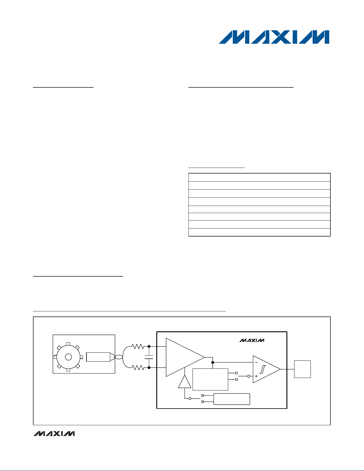
ENGINE BLOCK
MAX9924
VR SENSOR
DIFFERENTIAL
AMPLIFIER
ADAPTIVE/MINIMUM
AND
ZERO-CROSSING
THRESHOLDS
INTERNAL/EXTERNAL
BIAS VOLTAGE
μC

MAX9924–MAX9927
Variable Reluctance Sensor Interfaces with
Differential Input and Adaptive Peak Threshold
2 _______________________________________________________________________________________
ABSOLUTE MAXIMUM RATINGS
ELECTRICAL CHARACTERISTICS
(VCC= 5V, V
GND
= 0V, MAX9925/MAX9927 gain setting = 1V/V, Mode A1, V
BIAS
= 2.5V, V
PULLUP
= 5V, R
PULLUP
= 1kΩ, C
COUT
=
50pF. T
A
= T
MIN
to T
MAX
, unless otherwise noted. Typical values are at TA= +25°C.) (Note 2)
Stresses beyond those listed under “Absolute Maximum Ratings” may cause permanent damage to the device. These are stress ratings only, and functional
operation of the device at these or any other conditions beyond those indicated in the operational sections of the specifications is not implied. Exposure to
absolute maximum rating conditions for extended periods may affect device reliability.
VCCto GND.............................................................-0.3V to + 6V
All Other Pins..............................................-0.3V to (V
CC
+ 0.3V)
Current into IN+, IN-, IN_+, IN_-.......................................±40mA
Current into All Other Pins ................................................±20mA
Output Short-Circuit (OUT_, OUT) to GND.............................10s
Continuous Power Dissipation (T
A
= +70°C) (Note 1)
10-Pin µMAX (derate 8.8mW/°C above +70°C) ........707.3mW
16-Pin QSOP (derate 9.6mW/°C above +70°C)........771.5mW
Operating Temperature Range .........................-40°C to +125°C
Junction Temperature......................................................+150°C
Storage Temperature Range .............................-65°C to +150°C
Lead Temperature (soldering, 10s) .................................+300°C
Soldering Temperature (reflow) .......................................+260°C
Note 1: Package thermal resistances were obtained using the method described in JEDEC specification JESD51-7, using a four-layer
board. For detailed information on package thermal considerations, refer to www.maxim-ic.com/thermal-tutorial
.
µMAX
Junction-to-Ambient Thermal Resistance (θ
JA
) ......113.1°C/W
Junction-to-Case Thermal Resistance (θ
JC
) ................42°C/W
QSOP
Junction-to-Ambient Thermal Resistance (θ
JA
) ......103.7°C/W
Junction-to-Case Thermal Resistance (θ
JC
) ................37°C/W
PACKAGE THERMAL CHARACTERISTICS (Note 1)
POWER SUPPLY
Operating Supply Range V
Supply Current I
Power-On Time P
INPUT OPERATIONAL AMPLIFIER (MAX9925/MAX9927)
Input Voltage Range IN+, IN- Guaranteed by CMRR 0 V
Input Offset Voltage V
Input Bias Current I
Input Offset Current I
Common-Mode Rejection Ratio CMRR From VCM = 0 to V
Power-Supply Rejection Ratio PSRR
Output Voltage Low V
Output Voltage High V
Recovery Time from Saturation t
Gain-Bandwidth Product GBW 1.4 MHz
Slew Rate SR 2.3 V/µs
Charge-Pump Frequency f
PARAMETER SYMBOL CONDITIONS MIN TYP MAX UNITS
CC
CC
ON
OS-OA
BIAS
OFFSET
OL
OH
SAT
CP
(Note 3) 4.5 5.5 V
MAX9924/MAX9925 2.6 5
MAX9926/MAX9927 4.7 10
VCC > V
~ 1µs
Temperature drift 5 µV/° C
(Note 4) 0.1 6 nA
(Note 4) 0.05 2 nA
MAX9925 88 105
MAX9927 77 94
IOL = 1mA 0.050 V
IOH = -1mA
To 1% of the actual V
saturates
= 4.1V, step time for V
UVLO
CC
after output
OUT
CC
75 102 dB
V
CC
0.050
30 150 µs
0.5 3 mV
-
1.2 µs
1.3 MHz
CC
mA
V
dB
V
MAX9924–MAX9927
Variable Reluctance Sensor Interfaces with
Differential Input and Adaptive Peak Threshold
_______________________________________________________________________________________ 3
ELECTRICAL CHARACTERISTICS (continued)
(VCC= 5V, V
GND
= 0V, MAX9925/MAX9927 gain setting = 1V/V, Mode A1, V
BIAS
= 2.5V, V
PULLUP
= 5V, R
PULLUP
= 1kΩ, C
COUT
=
50pF. T
A
= T
MIN
to T
MAX
, unless otherwise noted. Typical values are at TA= +25°C.) (Note 2)
INPUT DIFFERENTIAL AMPLIFIER (MAX9924/MAX9926)
Input Voltage Range IN+, IN- Guaranteed by CMRR -0.3
Differential Amplifier
Common-Mode Rejection Ratio
Input Resistance R
ADAPTIVE PEAK DETECTION
Zero-Crossing Threshold V
Fixed and Adaptive Peak
Threshold
PARAMETER SYMBOL CONDITIONS MIN TYP MAX UNITS
CMRR
IN
ZERO_THRESH
V
ADAPTIVE
V
MIN-THRESH
MAX9924 (Note 5) 60 87
MAX9926 (Note 5) 55 78
(Note 5) 65 100 135 kΩ
Mode B
operation
(Notes 5, 6) MAX9926/MAX9927 -6.5 0 +10
Adaptive peak threshold 33 %PK
Minimum threshold of hysteresis
comparator MAX9924/MAX9926
(Notes 5, 6)
Minimum threshold of hysteresis
comparator MAX9925/MAX9927
(Notes 5, 6)
V
MIN-THRESH
MAX9924 (Notes 5, 6)
V
MIN-THRESH
MAX9926 (Notes 5, 6)
V
MIN-THRESH
MAX9925/MAX9927 (Notes 5, 6)
MAX9924/MAX9925 -6.5 0 +6.5
- V
ZERO-THRESH
- V
ZERO-THRESH
- V
ZERO-THRESH
for
for
for
41530
20 30 50
71526
21530
19 30 50
V
+
CC
0.3
V
dB
mV
mV
Watchdog Timeout for Adaptive
Peak Threshold
ENTIRE SYSTEM
Comparator Output Low Voltage V
Propagation Delay
COUT Transition Time t
Propagation Delay Jitter t
t
WD
COUT_OL
t
PDZ
t
PDA
HL-LH
PD-JITTER
Timing window to reset the adaptive
peak threshold if not triggered (input
level below threshold)
Overdrive = 2V to 3V, zero-crossing
Overdrive = 2V to 3V, adaptive peak
Includes noise of differential amplifier
and comparator, f = 10kHz,
V
IN
= 1V
sine wave
P-P
45 85 140 ms
0.2 V
50
150
2ns
20 ns
ns
MAX9924–MAX9927
Variable Reluctance Sensor Interfaces with
Differential Input and Adaptive Peak Threshold
4 _______________________________________________________________________________________
ELECTRICAL CHARACTERISTICS (continued)
(VCC= 5V, V
GND
= 0V, MAX9925/MAX9927 gain setting = 1V/V, Mode A1, V
BIAS
= 2.5V, V
PULLUP
= 5V, R
PULLUP
= 1kΩ, C
COUT
=
50pF. T
A
= T
MIN
to T
MAX
, unless otherwise noted. Typical values are at TA= +25°C.) (Note 2)
Note 2: Specifications are 100% tested at T
A
= +125°C, unless otherwise noted. All temperature limits are guaranteed by design.
Note 3: Inferred from functional PSRR.
Note 4: CMOS inputs.
Note 5: Guaranteed by design.
Note 6: Includes effect of V
OS
of internal op amp and comparator.
EXT
EXT Voltage Range V
Input Current to EXT I
DIRN (MAX9926 Only)
Output Low Voltage 0.2 V
INT_THRS, ZERO_EN
Low Input V
High Input V
Input Leakage I
Input Current ZERO_EN I
Switching Time Between Modes
A1, A2, and Modes B, C
BIAS
Input Current to BIAS I
BIAS Voltage Range V
Internal BIAS Reference Voltage V
PARAMETER SYMBOL CONDITIONS MIN TYP MAX UNITS
Mode B, TA = +125°C 1.5
EXT
Mode C, TA = +125°C 0.14
EXT
IL
IH
LEAK
SINK
t
SW
BIAS
BIAS
INT_BIAS
Mode B, V
Pullup resistor = 10kΩ,
V
ZERO_EN
With INT_THRS = GND, auto peakdetect is disabled, and EXT_THRS is
active
Modes A1, A2, B, C 1 µA
Modes A1, B, TA = +125°C 1.5
Mode C, TA = +125°C 0.2
Mode A2 (MAX9924/MAX9926) 2.46 V
EXT
= V
> V
GND
BIAS
; and Mode C 10 µA
0.7 x
V
CC
V
CC
- 1.1
V
CC
- 1.1
0.3 x
V
CC
1µA
500 800 µA
3µs
V
CC
- 1.1
V
CC
- 1.1
V
V
V
V
MAX9924–MAX9927
Variable Reluctance Sensor Interfaces with
Differential Input and Adaptive Peak Threshold
_______________________________________________________________________________________ 5
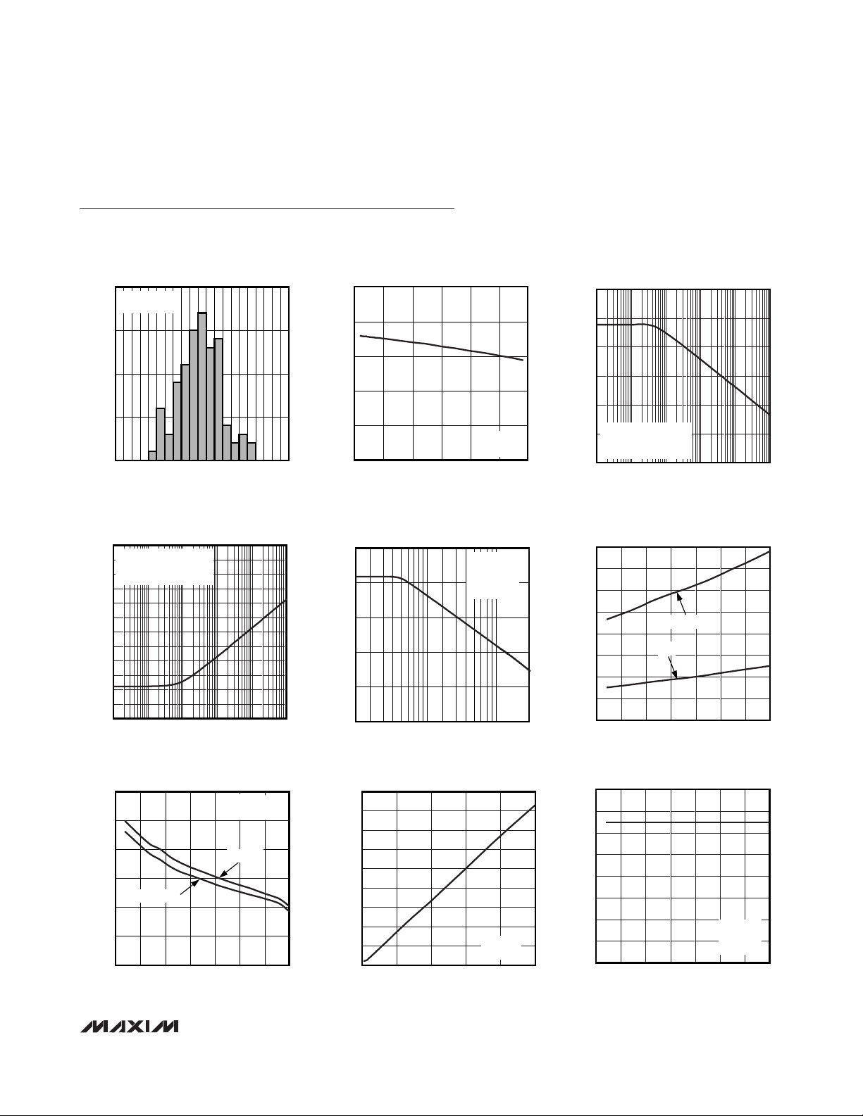
Typical Operating Characteristics
(VCC= 5V, V
GND
= 0V, MAX9925/MAX9927 gain setting = 1V/V. All values are at TA= +25°C, unless otherwise noted.)
INPUT OFFSET VOLTAGE DISTRIBUTION
20
VCM = 0
BIN SIZE = 250
15
10
PERCENTAGE OF UNITS (%)
5
0
-2000
-1500
-1000
0
500
1000
-500
INPUT OFFSET VOLTAGE (μV)
POWER-SUPPLY REJECTION RATIO
vs. FREQUENCY
0
V
= 100mV
RIPPLE
-10
V
BIAS
-20
INPUTS COUPLED TO GND
-30
-40
-50
-60
PSSR (dB)
-70
-80
-90
-100
-110
-120
1 100k
= V
OUT
P-P
= 2.5V
FREQUENCY (Hz)
INPUT OFFSET VOLTAGE
vs. TEMPERATURE
0.6
0.5
0.4
0.3
0.2
INPUT OFFSET VOLTAGE (mV)
0.1
VCM = 2.5V
0
-50 25 50-25 0 75 100 125
TEMPERATURE (°C)
1500
V
MAX9925
VCM = 0
2000
10k1k10010
OUT
2500
= 2.5V
3000
vs. INPUT COMMON-MODE VOLTAGE
0.5
MAX9924 toc01
0.4
0.3
0.2
INPUT OFFSET VOLTAGE (mV)
0.1
0
-0.5 1.50.5 2.5 3.5 4.5 5.5
125
MAX9924 toc04
100
75
GAIN (dB)
50
25
0
0.001 10
900
MAX9924 toc07
800
700
600
500
400
300
200
ADAPTIVE THRESHOLD LEVEL (mV)
100
0
02.5
INPUT OFFSET VOLTAGE
V
= 2.5V
OUT
MAX9925
INPUT COMMON-MODE VOLTAGE (V)
OPEN LOOP FREQUENCY
RESPONSE
VCC = 5V
= 2.5V
V
BIAS
= 2V
V
OUT
P-P
MAX9925
0.1
FREQUENCY (kHz)
ADAPTIVE THRESHOLD AND RATIO
vs. SIGNAL LEVEL
fIN = 1kHz
MAX9924
1.5 2.01.00.5
SIGNAL LEVEL (VP)
MAX9924 toc02
MAX9924 toc05
MAX9924 toc08
COMMON-MODE REJECTION RATIO
120
100
80
60
CMRR (dB)
40
V
20
V
CMRR = 20log(ADM/ACM)
0
1100k
40
35
30
25
(mV)
OH
20
AND V
15
OL
V
10
5
0
-50 125
400
350
300
250
200
150
THRESHOLD (mV)
100
50
0
-50 125
vs. FREQUENCY
= V
= 2.5V
BIAS
OUT
= 2V
CM
P-P
10k1k10010
FREQUENCY (Hz)
VOL AND VOH vs. TEMPERATURE
VCC - V
OH
VOL
50 75 100250-25
TEMPERATURE (°C)
ADAPTIVE THRESHOLD
vs. TEMPERATURE
VIN = 2V
fIN = 1kHz
MAX9924
25 50 75 1000-25
TEMPERATURE (°C)
MAX9924 toc03
MAX9924 toc06
MAX9924 toc09
P-P

MAX9924–MAX9927
Variable Reluctance Sensor Interfaces with
Differential Input and Adaptive Peak Threshold
6 _______________________________________________________________________________________
Typical Operating Characteristics (continued)
(VCC= 5V, V
GND
= 0V, MAX9925/MAX9927 gain setting = 1V/V. All values are at TA= +25°C, unless otherwise noted.)
-5
5
0
15
10
25
20
30
-50 0 25-25 50 75 100 125
MINIMUM AND ZERO-CROSSING
THRESHOLD vs. TEMPERATURE
MAX9924 toc10
TEMPERATURE (°C)
THRESHOLD (mV)
VCM = 2.5V
f
IN
= 5Hz
ZERO CROSSING
AT 5Hz
MINIMUM THRESHOLD
ZERO CROSSING
AT 1Hz
0
25
50
75
100
CMRR vs. TEMPERATURE
MAX9924 toc11
TEMPERATURE (°C)
CMRR (dB)
-50 25 50-25 0 75 100 125
MAX9924
V
CM
= 0 TO 5V
INPUT SIGNAL vs. COUT WITH
WATCHDOG TIMER EXPIRED
MAX9924 toc12
20ms/div
V
BIAS
5V
fIN = 5Hz
COUT
INPUT SIGNAL
INPUT SIGNAL vs. COUT WITH
WATCHDOG TIMER EXPIRED
MAX9924 toc13
100μs/div
V
BIAS
5V
fIN = 1kHz
COUT
INPUT SIGNAL
833mV
MAX9924 toc14
100μs/div
OVERDRIVEN INPUT VOLTAGES
(MAX9924)
MAX9924 toc15
200μs/div
DIRN OPERATION
(MAX9924)
INPUT REFERRED NOISE DENSITY
vs. FREQUENCY
100
80
60
40
INPUT VOLTAGE NOISE (nV/ Hz)
20
10
10 1k100 10k 100k 1M
FREQUENCY (Hz)
MAX9924 toc16

MAX9924–MAX9927
Variable Reluctance Sensor Interfaces with
Differential Input and Adaptive Peak Threshold
_______________________________________________________________________________________ 7
Pin Description
PIN
MAX9924 MAX9925 MAX9926 MAX9927
1 1 — — IN+ Noninverting Input
2 2 — — IN- Inverting Input
— 3 — — OUT Amplifier Output
3 — — — N.C. No Connection. Not internally connected.
4 4 — — BIAS
5 5 11 11 GND Ground
6 6 13 — ZERO_EN
7 7 — — COUT
8 8 — — EXT
9 9 — — INT_THRS Internal Adaptive Threshold. Mode configuration pin.
10 10 14 14 V
— — 1 1 INT_THRS1 Internal Adaptive Threshold 1. Mode configuration pin.
— — 2 2 EXT1
— — 3 3 BIAS1
— — 4 4 COUT1
— — 5 5 COUT2
— — 6 6 BIAS2
— — 7 7 EXT2
— — 8 8 INT_THRS2 Internal Adaptive Threshold 2. Mode configuration pin.
— — 9 9 IN2+ Noninverting Input 2
— — 10 10 IN2- Inverting Input 2
— — 12 — DIRN
— — — 12 OUT2 Amplifier Output 2
— — — 13 OUT1 Amplifier Output 1
— — 15 15 IN1- Noninverting Input 1
— — 16 16 IN1+ Inverting Input 1
NAME FUNCTION
Input Bias. Connect to an external resistor-divider and bypass
to ground with a 0.1µF and 10µF capacitor.
Zero-Crossing Enable. Mode configuration pin, internally
with 10kΩ resistor.
CC
PULLUP
.
PULLUP
PULLUP
PULLUP
CC
pulled up to V
Comparator Output. Open-drain output, connect a 10kΩ pullup
resistor from COUT to V
External Reference Input. Leave EXT unconnected in Modes
A1, A2. Apply an external voltage in Modes B, C.
Power Supply
External Reference Input 1. Leave EXT unconnected in Modes
A1, A2. Apply an external voltage in Modes B, C.
Input Bias 1. Connect to an external resistor-divider and
bypass to ground with a 0.1µF and 10µF capacitor.
Comparator Output 1. Open-drain output, connect a 10kΩ
pullup resistor from COUT1 to V
Comparator Output 2. Open-drain output, connect a 10kΩ
pullup resistor from COUT2 to V
Input Bias 2. Connect to an external resistor-divider and
bypass to ground with a 0.1µF and 10µF capacitor.
External Reference Input 2. Leave EXT unconnected in Modes
A1, A2. Apply an external voltage in Modes B, C.
Rotational Direction Output. Open-drain output, connect a
pullup resistor from DIRN to V
.
.
.
MAX9924–MAX9927
Variable Reluctance Sensor Interfaces with
Differential Input and Adaptive Peak Threshold
8 _______________________________________________________________________________________
Functional Diagrams
V
CC
IN-
IN+
REFERENCE
BIAS
V
CC
INTERNAL
2.5V
100kΩ
100kΩ
100kΩ
BUFFER
PEAK
DETECTOR
MODE
LOGIC
INT_THRS EXT
100kΩ
OP AMP
30%
V
MIN
THRESHOLD
MAX9924
COMPARATOR
MODE
LOGIC
65ms
WATCHDOG
V
CC
10kΩ
V
CC
GND
COUT
ZERO_EN
INT_THRS

MAX9924–MAX9927
Variable Reluctance Sensor Interfaces with
Differential Input and Adaptive Peak Threshold
_______________________________________________________________________________________ 9
Functional Diagrams (continued)
IN+
BIAS
OUT
V
CC
IN-
V
CC
OP AMP
BUFFER
30%
PEAK
DETECTOR
V
MIN
THRESHOLD
MAX9925
COMPARATOR
MODE
LOGIC
85ms
WATCHDOG
V
CC
10kΩ
V
CC
GND
COUT
ZERO_EN
INT_THRS
EXT
MAX9924–MAX9927
Variable Reluctance Sensor Interfaces with
Differential Input and Adaptive Peak Threshold
10 ______________________________________________________________________________________
Functional Diagrams (continued)
V
CC
IN1-
IN1+
BIAS1
EXT1
IN2-
IN2+
V
V
CC
V
100kΩ
CC
100kΩ
100kΩ
INTERNAL
REFERENCE
2.5V
BUFFER
100kΩ
CC
100kΩ
OP AMP
PEAK
DETECTOR
OP AMP
100kΩ
100kΩ
30%
V
MIN
THRESHOLD
MAX9926
COMPARATOR
FLIP-FLOP
DIRN
CLK
85ms
WATCHDOG
V
CC
GND
COUT1
DIRN
BIAS2
EXT2
100kΩ
BUFFER
PEAK
DETECTOR
30%
V
MIN
THRESHOLD
COMPARATOR
MODE
LOGIC
85ms
WATCHDOG
V
CC
10kΩ
COUT2
ZERO_EN
INT_THRS1
INT_THRS2

MAX9924–MAX9927
Variable Reluctance Sensor Interfaces with
Differential Input and Adaptive Peak Threshold
______________________________________________________________________________________ 11
Functional Diagrams (continued)
IN1-
IN1+
BIAS1
OUT1
V
CC
V
CC
OP AMP
BUFFER
30%
PEAK
DETECTOR
V
MIN
THRESHOLD
V
CC
MAX9927
COMPARATOR
85ms
WATCHDOG
V
CC
GND
COUT1
EXT1
IN2-
IN2+
BIAS2
V
CC
OUT1
COUT2
INT_THRS1
INT_THRS2
BUFFER
OP AMP
PEAK
DETECTOR
30%
EXT2
V
MIN
THRESHOLD
COMPARATOR
85ms
WATCHDOG
MODE
LOGIC

MAX9924–MAX9927
Variable Reluctance Sensor Interfaces with
Differential Input and Adaptive Peak Threshold
12 ______________________________________________________________________________________
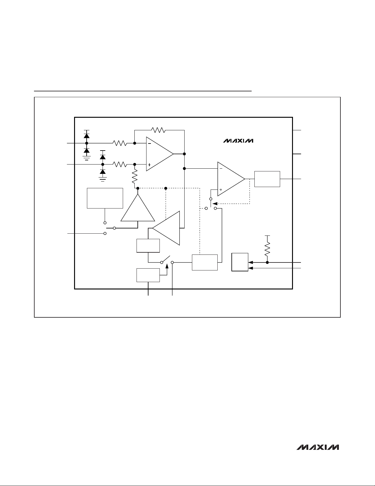
Detailed Description
The MAX9924–MAX9927 interface with variable reluctance (VR) or magnetic coil sensors. These devices
produce accurate pulses aligned with flywheel gearteeth even when the pickup signal is small and in the
presence of large amounts of system noise. They interface with new-generation differential VR sensors as well
as legacy single-ended VR sensors.
The MAX9924/MAX9925 integrate a precision op amp,
a precision comparator, an adaptive peak threshold
block, a zero-crossing detection circuit, and precision
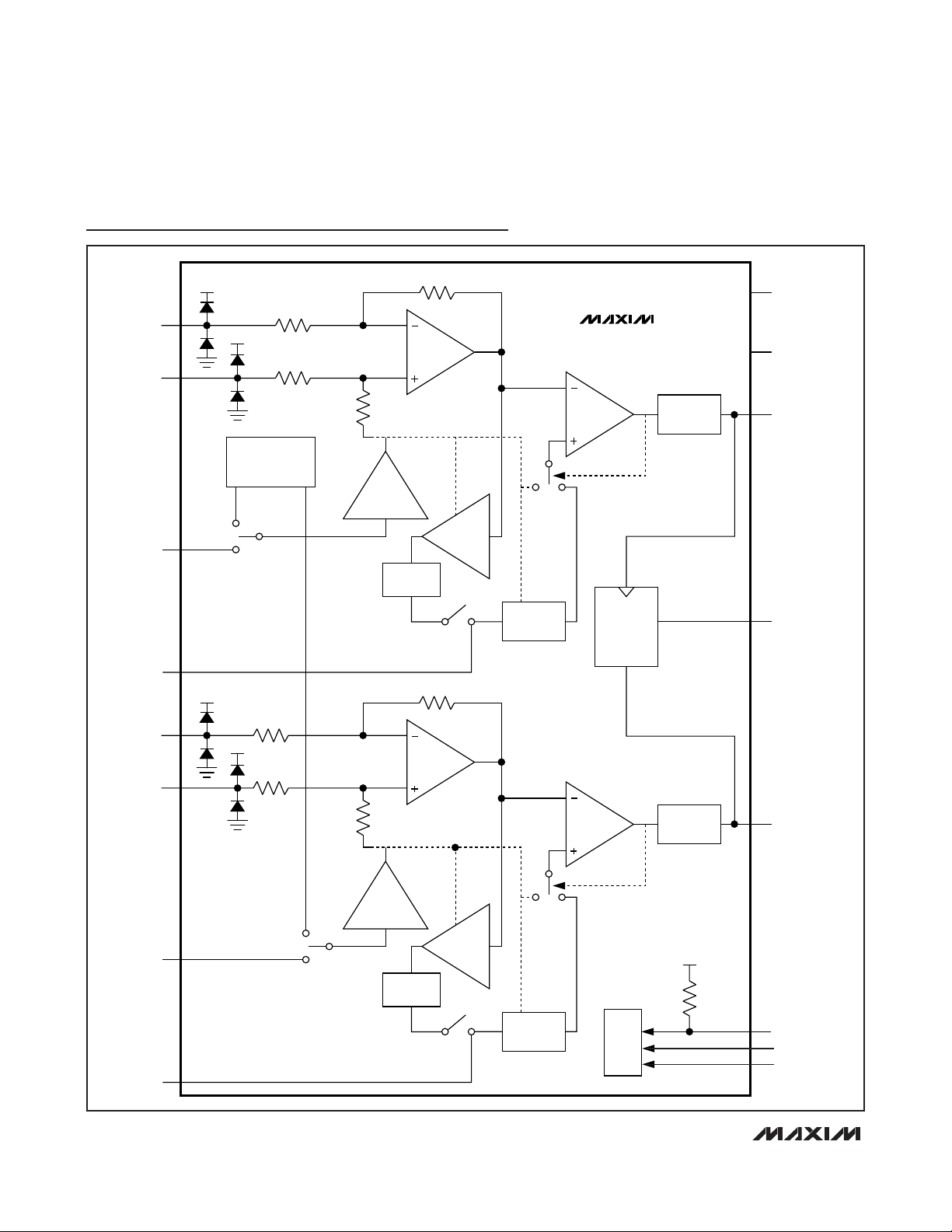
matched resistors (MAX9924). The MAX9926 and
MAX9927 are dual versions of the MAX9924 and
MAX9925, respectively. The MAX9926 also provides a
rotational output that is useful for quadrature-connected
VR sensors used in certain high-performance engines.
The input op amp in the MAX9925/MAX9927 are typically configured as a differential amplifier by using four
external resistors (the MAX9924/MAX9926 integrate
precision-matched resistors to give superior CMRR performance). This input differential amplifier rejects input
common-mode noise and converts the input differential
signal from a VR sensor into a single-ended signal. The
internal comparator produces output pulses by compar-
ing the output of the input differential amplifier with a
threshold voltage that is set depending on the mode
that the device is in (see the
Mode Selection
section).
Mode Selection
The MAX9924/MAX9926 provide four modes of operation: Mode A1, Mode A2, Mode B, and Mode C as determined by voltages applied to inputs ZERO_EN and
INT_THRS (see Tables 1, 2, and 3). In Modes A1 and
A2, the internal adaptive peak threshold and the zerocrossing features are enabled. In Mode A2, an internally
generated reference voltage is used to bias the differential amplifier and all internal circuitry instead of an external voltage connected to the BIAS input—this helps
reduce external components and design variables leading to a more robust application. In Mode B, the adaptive peak threshold functionality is disabled, but
zero-crossing functionality is enabled. In this mode, an
external threshold voltage is applied at EXT allowing
application-specific adaptive algorithms to be implemented in firmware. In Mode C, both the adaptive peak
threshold and zero-crossing features are disabled and
the device acts as a high-performance differential amplifier connected to a precision comparator (add external
hysteresis to the comparator for glitch-free operation).
Table 1. MAX9924/MAX9926 Operating Modes
Table 2. MAX9925 Operating Modes
Table 3. MAX9927 Operating Modes
OPERATING MODE
A1 V
A2 GND GND Enabled Enabled Internal Ref
BVCCGND Enabled Disabled External
C GND V
ZERO_EN INT_THRS ZERO CROSSING
SETTING DEVICE FUNCTIONALITY
CC
V
CC
CC
ADAPTIVE PEAK
THRESHOLD
Enabled Enabled External
Disabled Disabled External
BIAS VOLTAGE
SOURCE
OPERATING MODE
A1 V
BVCCGND Enabled Disabled
C GND V
ZERO_EN INT_THRS ZERO CROSSING ADAPTIVE PEAK THRESHOLD
SETTING DEVICE FUNCTIONALITY
CC
V
CC
CC
Enabled Enabled
Disabled Disabled
OPERATING MODE
A1 V
B GND Enabled Disabled
SETTING DEVICE FUNCTIONALITY
INT_THRS ZERO CROSSING ADAPTIVE PEAK THRESHOLD
CC
Enabled Enabled

Differential Amplifier
The input operational amplifier is a rail-to-rail input and
output precision amplifier with CMOS input bias currents, low offset voltage (VOS) and drift. A novel input
architecture eliminates crossover distortion at the operational amplifier inputs normally found in rail-to-rail input
structures. These features enable reliable small-signal
detection for VR sensors.
The MAX9924/MAX9926 include on-chip precisionmatched low-ppm resistors configured as a differential
amplifier. High-quality matching and layout of these
resistors produce extremely high DC and AC CMRR
that is important to maintain noise immunity. The
matched ppm-drift of the resistors guarantees performance across the entire -40°C to +125°C automotive
temperature range.
Bias Reference
In Modes A1, B, and C, a well-decoupled external
resistor-divider generates a VCC/2 signal for the BIAS
input that is used to reference all internal electronics in
the device. BIAS should be bypassed with a 0.1µF and
10µF capacitor in parallel with the lower half of the
resistor-divider forming a lowpass filter to provide a stable external BIAS reference.
The minimum threshold, adaptive peak threshold, zerocrossing threshold signals are all referenced to this
voltage. An input buffer eliminates loading of resistordividers due to differential amplifier operation. Connect
BIAS to ground when operating in Mode A2. An internal
(2.5V typical) reference is used in Mode A2, eliminating
external components.
Adaptive Peak Threshold
Modes A1 and A2 in the MAX9924–MAX9927 use an
internal adaptive peak threshold voltage to trigger the
output comparator. This adaptive peak threshold voltage scheme provides robust noise immunity to the input
VR signal, preventing false triggers from occurring due
to broken tooth or off-centered gear-tooth wheel. See
Figure 1.
The sensor signal at the output of the differential gain
stage is used to generate a cycle-by-cycle adaptive
peak threshold voltage. This threshold voltage is 1/3 of
the peak of the previous cycle of the input VR signal. As
the sensor signal peak voltage rises, the adaptive peak
threshold voltage also increases by the same ratio.
Conversely, decreasing peak voltage levels of the input
VR signal causes the adaptive peak threshold voltage
used to trigger the next cycle also to decrease to a new
lower level. This threshold voltage then provides an
arming level for the zero-crossing circuit of the comparator (see the
Zero Crossing
section).
If the input signal voltage remains lower than the adaptive peak threshold for more than 85ms, an internal
watchdog timer drops the threshold level to a default
minimum threshold (V
MIN_THRESH
). This ensures pulse
recognition recovers even in the presence of intermittent sensor connection.
The internal adaptive peak threshold can be disabled
and directly fed from the EXT input. This mode of operation is called Mode B, and allows implementations of custom threshold algorithms in firmware. This EXT voltage is
typically generated by filtering a PWM-modulated output
from an onboard microcontroller (µC). An external operational amplifier can also be used to construct an active
lowpass filter to filter the PWM-modulated EXT signal.
MAX9924–MAX9927
Variable Reluctance Sensor Interfaces with
Differential Input and Adaptive Peak Threshold
______________________________________________________________________________________ 13
Figure 1. Adaptive Peak Threshold Operation
ADAPTIVE
THRESHOLD
SET BY V1
SIGNAL
1
V1
VR
V1
3
V2
ADAPTIVE
THRESHOLD
SET BY V2
1/3 V2
MIN
THRESHOLD
COUT
20ms
40ms 60ms
85ms
80ms 100ms 120ms 140ms 160ms
180ms 200ms

MAX9924–MAX9927
Zero Crossing
The zero-crossing signal provides true timing information for engine-control applications. The zero-voltage
level in the VR sensor signal corresponds to the center
of the gear-tooth and is the most reliable marker for
position/angle-sensing applications. Since the output of
the differential amplifier is level-shifted to the BIAS voltage, the zero of the input VR signal is simply BIAS. The
comparator output state controls the status of the input
switch that changes the voltage at its noninverting input
from the adaptive/external threshold level to the BIAS
level. The difference in these two voltages then effectively acts as hysteresis for the comparator, thus providing noise immunity.
Comparator
The internal comparator is a fast open-drain output
comparator with low input offset voltage and drift. The
comparator precision affects the ability of the signal
chain to resolve small VR sensor signals. An open-drain
output allows the comparator to easily interface to a
variety of µC I/O voltages.
When operating the MAX9924/MAX9925/MAX9926 in
Mode C, external hysteresis can be provided by adding
external resistors (see Figures 5 and 8). The high and
low hysteresis thresholds in Mode C can be calculated
using the following equations,
and
Rotational Direction Output
(MAX9926 Only)
For quadrature-connected VR sensors, the open-drain
output DIRN indicates the rotational direction of inputs
IN1 and IN2 based on the output state of COUT1 and
COUT2. DIRN goes high when COUT1 is leading
COUT2, and low when COUT1 is following COUT2.
Applications Information
Bypassing and Layout Considerations
Good power-supply decoupling with high-quality
bypass capacitors is always important for precision
analog circuits. The use of an internal charge pump for
the front-end amplifier makes this more important.
Bypass capacitors create a low-impedance path to
ground for noise present on the power supply.
The minimum impedance of a capacitor is limited to the
effective series resistance (ESR) at the self-resonance
frequency, where the effective series inductance (ESL)
cancels out the capacitance. The ESL of the capacitor
dominates past the self-resonance frequency resulting
in a rise in impedance at high frequencies.
Bypass the power supply of the MAX9924–MAX9927
with multiple capacitor values in parallel to ground. The
use of multiple values ensures that there will be multiple
self-resonance frequencies in the bypass network, lowering the combined impedance over frequency. It is
recommended to use low-ESR and low-ESL ceramic
surface-mount capacitors in a parallel combination of
10nF, 0.1µF and 1µF, with the 10nF placed closest
between the VCCand GND pins. The connection
between these capacitor terminals and the power-supply pins of the part (both V
CC
and GND) should be
through wide traces (preferably planes), and without
vias in the high-frequency current path.
Variable Reluctance Sensor Interfaces with
Differential Input and Adaptive Peak Threshold
14 ______________________________________________________________________________________
⎛
RV V
1
()
V
TH
PULLUP BIAS
=
⎜
RR R
++
12
⎝
V
=
TL BIAS
2
R
⎛
⎜
⎝
+
12
RR
−
PULLUP
⎞
V
+
BIAS
⎟
⎠
⎞
×
V
⎟
⎠
MAX9924–MAX9927
Variable Reluctance Sensor Interfaces with
Differential Input and Adaptive Peak Threshold
______________________________________________________________________________________ 15
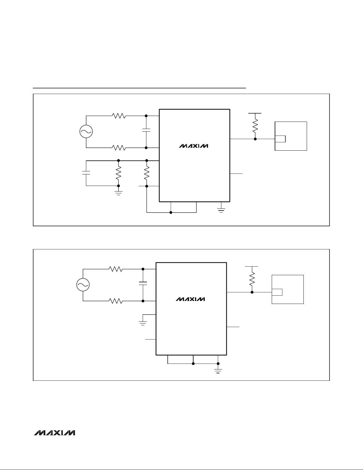
Application Circuits
Figure 2. MAX9924/MAX9926 Operating Mode A1
Figure 3. MAX9924/MAX9926 Operating Mode A2
10kΩ
VR
SENSOR
10kΩ
10μF || 0.1μF
1nF
1kΩ1kΩ
+5V
IN+
IN-
MAX9924
BIAS
V
CC
ZERO_EN INT_THRS GND
MAX9926
COUT
EXT
V
PULLUP
R
PULLUP
μC
TPU
10kΩ
VR
SENSOR
10kΩ
1nF
+5V
IN+
IN-
MAX9924
BIAS
V
CC
ZERO_EN INT_THRS GND
MAX9926
COUT
EXT
R
PULLUP
V
PULLUP
μC
TPU

MAX9924–MAX9927
Variable Reluctance Sensor Interfaces with
Differential Input and Adaptive Peak Threshold
16 ______________________________________________________________________________________
Application Circuits (continued)
Figure 4. MAX9924/MAX9926 Operating Mode B
Figure 5. MAX9924/MAX9926 Operating Mode C
10kΩ
VR
SENSOR
10kΩ
10μF || 0.1μF
1nF
1kΩ1kΩ
+5V
10kΩ
VR
SENSOR
10kΩ
1nF
IN+
IN-
MAX9924
BIAS
V
CC
ZERO_EN INT_THRS GND
IN+
IN-
MAX9926
MAX9924
BIAS
MAX9926
COUT
EXT
COUT
R
PULLUP
R
PULLUP
R2
V
PULLUP
FILTER
V
PULLUP
μC
TPU
PWM
μC
TPU
+5V
1kΩ1kΩ
V
CC
ZERO_ENINT_THRS
R1
EXT
GND
10μF || 0.1μF

MAX9924–MAX9927
Variable Reluctance Sensor Interfaces with
Differential Input and Adaptive Peak Threshold
______________________________________________________________________________________ 17
Application Circuits (continued)
Figure 6. MAX9925/MAX9927 Operating Mode A
Figure 7. MAX9925/MAX9927 Operating Mode B
10kΩ
VR
SENSOR
10μF || 0.1μF
1nF
10kΩ
1kΩ1kΩ
+5V
IN-
IN+
BIAS
V
CC
ZERO_EN INT_THRS GND
OUT
MAX9925
MAX9927
COUT
EXT
R
PULLUP
V
PULLUP
μC
TPU
10kΩ
VR
SENSOR
10μF || 0.1μF
1nF
10kΩ
1kΩ1kΩ
+5V
IN-
IN+
OUT
MAX9925
MAX9927
BIAS
V
CC
ZERO_EN INT_THRS GND
COUT
EXT
R
PULLUP
V
PULLUP
FILTER
μC
TPU
PWM

MAX9924–MAX9927
Variable Reluctance Sensor Interfaces with
Differential Input and Adaptive Peak Threshold
18 ______________________________________________________________________________________
Application Circuits (continued)
Figure 8. MAX9925 Operating Mode C
10kΩ
VR
SENSOR
10μF || 0.1μF
1nF
10kΩ
1kΩ1kΩ
+5V
IN-
IN+
BIAS
V
CC
OUT
MAX9925
ZERO_ENINT_THRS
R1
COUT
GND
EXT
R
PULLUP
V
R2
PULLUP
μC
TPU

MAX9924–MAX9927
Variable Reluctance Sensor Interfaces with
Differential Input and Adaptive Peak Threshold
______________________________________________________________________________________ 19
Typical Operating Circuit
VR SENSOR
V
CC
IN-
IN+
REFERENCE
VOLTAGE = 2 x V
BIAS
*THE MAX9924 IS
CONFIGURED IN MODE A2.
V
CC
BANDGAP
100kΩ
100kΩ
BG
100kΩ
BUFFER
INT_THRS
OP AMP
PEAK
DETECTOR
MODE
LOGIC
100kΩ
30%
EXT
4.5V TO 5.5V
V
THRESHOLD
CC
MAX9924
COMPARATOR
V
MIN
MODE
LOGIC
WATCHDOG
GND
85ms
V
CC
10kΩ
R
PULLUP
COUT
ZERO_EN
V
PULLUP
μC
TPU

MAX9924–MAX9927
Variable Reluctance Sensor Interfaces with
Differential Input and Adaptive Peak Threshold
20 ______________________________________________________________________________________
Pin Configurations
Chip Information
PROCESS: BiCMOS
Selector Guide
PART AMPLIFIER GAIN
MAX9924UAUB 1 x Differential 1V/V
MAX9925AUB 1 x Operational Externally Set
MAX9926UAEE 2 x Differential 1V/V
MAX9927AEE 2 x Operational Externally Set
TOP VIEW
IN_THRS1
EXT1
BIAS1
COUT1
COUT2
BIAS2
EXT2
INT_THRS2
1
2
3
4
5
6
7
8
+
MAX9926
16
15
14
13
12
11
10
9
QSOP
TOP VIEW
IN+
IN-
N.C.
+
1
2
3
MAX9924
4
5
10
9
8
7
6
μMAX
IN1+
IN1-
V
CC
ZERO_EN
DIRN
GND
IN2-
IN2+
V
CC
INT_THRS
EXT
COUTBIAS
ZERO_ENGND
IN_THRS1
EXT1
BIAS1
COUT1
COUT2
BIAS2
EXT2
INT_THRS2
IN+
IN-
OUT
1
2
3
4
5
6
7
8
1
2
3
4
5
+
MAX9927
QSOP
+
MAX9925
μMAX
16
15
14
13
12
11
10
9
10
9
8
7
6
IN1+
IN1-
V
CC
OUT1
OUT2
GND
IN2-
IN2+
V
CC
INT_THRS
EXT
COUTBIAS
ZERO_ENGND

MAX9924–MAX9927
Variable Reluctance Sensor Interfaces with
Differential Input and Adaptive Peak Threshold
______________________________________________________________________________________ 21
PACKAGE TYPE PACKAGE CODE OUTLINE NO. LAND PATTERN NO.
10 µMAX U10+2
21-0061 90-0330
16 QSOP E16+1
21-0055 90-0167
Package Information
For the latest package outline information and land patterns (footprints), go to www.maxim-ic.com/packages. Note that a “+”, “#”, or
“-” in the package code indicates RoHS status only. Package drawings may show a different suffix character, but the drawing pertains to the package regardless of RoHS status.
10LUMAX.EPS
α
α

MAX9924–MAX9927
Variable Reluctance Sensor Interfaces with
Differential Input and Adaptive Peak Threshold
22 ______________________________________________________________________________________
Package Information (continued)
For the latest package outline information and land patterns (footprints), go to www.maxim-ic.com/packages. Note that a “+”, “#”, or
“-” in the package code indicates RoHS status only. Package drawings may show a different suffix character, but the drawing pertains to the package regardless of RoHS status.

MAX9924–MAX9927
Variable Reluctance Sensor Interfaces with
Differential Input and Adaptive Peak Threshold
Maxim cannot assume responsibility for use of any circuitry other than circuitry entirely embodied in a Maxim product. No circuit patent licenses are
implied. Maxim reserves the right to change the circuitry and specifications without notice at any time.
Maxim Integrated Products, 120 San Gabriel Drive, Sunnyvale, CA 94086 408-737-7600 ____________________
Revision History
REVISION
NUMBER
0 10/08 Initial release —
1 2/09
2 3/09 Corrected various errors
3 17, 18
4 1
REVISION
DATE
Removed future product references for the MAX9926 and MAX9927, updated EC
table
3/11 Updated Figures 6, 7, and 8
3/12 Added automotive qualifies parts
DESCRIPTION
PAGES
CHANGED
1–4
2, 3, 4, 6, 13
23
.cnI ,stcudorP detargetnI mixaM fo kramedart deretsiger a si mixaM stcudorP detargetnI mixaM 2102©
 Loading...