

General Description
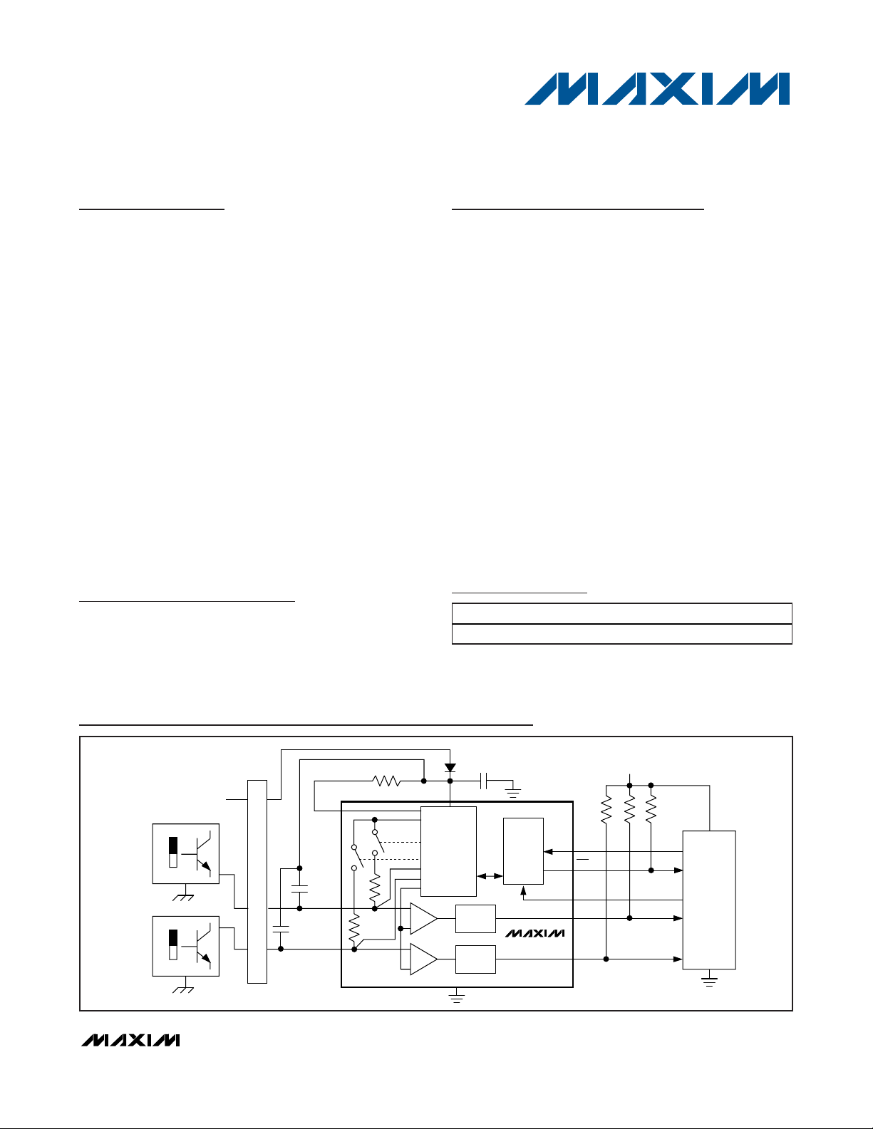
The MAX9921 provides a single chip solution to interface
two 2-wire Hall-effect sensors to a low-voltage microprocessor (µP). This device supplies and monitors the current drawn by two Hall-effect sensors, filters the sensed
current level, and outputs the corresponding logic level.
The MAX9921 includes input diagnostics and fault protection. These features allow the device to determine fault
conditions such as open inputs, inputs shorted to the battery, and inputs shorted to ground. If the MAX9921
detects any of these conditions at either IN1 or IN2, the
device shuts off the current to the corresponding input.
The MAX9921 protects the Hall sensors from supply transients up to 60V at the BAT supply. Normal operating
supply voltage ranges from 6V to 18V. If the battery voltage is out of range, the MAX9921 shuts off the current to
the Hall sensors.
The MAX9921 provides an 80µs blanking time following
Hall sensor power-up or restart. The open-drain logic
outputs are compatible with logic levels up to 5.5V.
The MAX9921 is available in a small 10-pin µMAX
®
package and is specified over the -40°C to +125°C
automotive temperature range.
Applications
Features
♦ Withstands 60V at BAT Supply and Hall Inputs
♦ 6V to 18V Operating Voltage Range
♦ Provides Supply Current and Interfaces to Two
2-Wire Hall Sensors
♦ Error Output with Diagnostics of Hall Inputs and
BAT Voltage
♦ Protects Hall Sensors from Overvoltage by
Isolating them from Supply Transients
♦ Hall Inputs Protected from Short to Ground
♦ Ramps Current to Hall Sensors at 4mA/µs
♦ Output Enable Input Allows Multiplexing of
Outputs from Multiple MAX9921s
♦ Hall Output Filtering
♦ Hall Sensor Blanking Following Hall Sensor
Power-Up and Restart
♦ Low-Power Shutdown, Controlled with OE and
DIAG Inputs
♦ Operates with ±2V Ground Shifts Between Hall
Sensor and MAX9921
MAX9921
Dual, 2-Wire Hall-Effect Sensor Interface
with Diagnostics
________________________________________________________________
Maxim Integrated Products
1
Ordering Information
N
REMOTE
GROUND
ISET
BATTERY
OE
ERR
DIAG
OUT1
OUT2
BAT
R
ISET
= 63.4kΩ, 1%
V
BAT
: 6V TO 18V OPERATING,
WITHSTANDS 60V
3.3V TO 5V
IN1
0.1μF
10kΩ
IN2
REF
GENERATION,
DIAGNOSTICS
AND
OVERVOLTAGE
DETECT
S
N
REMOTE
GROUND
S
0.01μF
CONTROL
FILTER
FILTER
μP/LOGIC
CIRCUIT
GND
V
CC
0.01μF
GND
MAX9921
E
C
U
C
O
N
N
E
C
T
O
R
Typical Application Circuit
19-4119; Rev 0; 6/08
For pricing, delivery, and ordering information, please contact Maxim Direct at 1-888-629-4642,
or visit Maxim’s website at www.maxim-ic.com.
+
Denotes a lead-free package.
T = Tape and reel.
µMAX is a registered trademark of Maxim Integrated Products, Inc.
Pin Configuration appears at end of data sheet.
Door Modules
Window Lifters
Seat Movers
Electric Sunroofs
Powered Lift Gate
Controllers
Powered Running Boards
Seatbelt Buckles
PART TEMP RANGE PIN-PACKAGE
MAX9921AUB+T -40°C to +125°C 10 µMAX
MAX9921
Dual, 2-Wire Hall-Effect Sensor Interface
with Diagnostics
2 _______________________________________________________________________________________
ABSOLUTE MAXIMUM RATINGS
DC ELECTRICAL CHARACTERISTICS
(V
BAT
= 13.6V, V
DIAG
= 0V, VOE= 5V, IN1 = IN2 = no connection, R
ISET
= 63.4kΩ, RPU= 10kΩ at ERR, OUT1 and OUT2, TA= -40°C
to +125°C, unless otherwise noted. Typical values are at T
A
= +25°C.) (Note 1)
Stresses beyond those listed under “Absolute Maximum Ratings” may cause permanent damage to the device. These are stress ratings only, and functional
operation of the device at these or any other conditions beyond those indicated in the operational sections of the specifications is not implied. Exposure to
absolute maximum rating conditions for extended periods may affect device reliability.
BAT to GND............................................................-0.3V to +60V
ISET to BAT ...........................................................-2.0V to +0.3V
IN1, IN2 to GND..........-5.0V to the lower of +60V or (V
BAT
+ 1V)
DIAG, OE to GND..................................................-0.3V to +6.0V
OUT1, OUT2, ERR to GND....................................-0.3V to +6.0V
Short-Circuit Duration of OUT1, OUT2, ERR to GND
or to 5.5V (individually)............................................Continuous
Current into Any Pin Except IN1, IN2 ...............................±20mA
Current into IN1, IN2.......................................................±100mA
Continuous Power Dissipation (T
A
= +70°C)
10-Pin µMAX (derate 5.6mW/°C above +70°C) .........444.4mW
Operating Temperature Range .........................-40°C to +125°C
Junction Temperature......................................................+150°C
Storage Temperature Range .............................-65°C to +150°C
Lead Temperature (soldering, 10s) .................................+300°C
PARAMETER SYMBOL CONDITIONS MIN TYP MAX UNITS
GENERAL
BAT Supply Range V
V
Low for ERR Output Active V
BAT
V
High for ERR Output Active V
BAT
BAT Supply Current
HALL INPUTS (IN1 and IN2)
Input Current for Output High I
Input Current for Output Low I
Input Current Hysteresis for
High/Low Detection
Input Pullup Impedance R
Input Voltage Interpreted as
Shorted to Battery
Current Range Interpreted as
Open Circuit
Current Level Interpreted as
Shorted Sensor to Ground
BAT
BL
BH
I
BAT
I
SD
I
IN,HYS
V
I
OC
I
SC
Normal mode 1 1.3 mA
Shutdown mode, VOE = V
IH
IL
V
PU
SB
BAT
I
= -14mA
IN
Measured with respect to V
Not a sustained condition, reverts to -50µA
when detected
= 6V, inputs IN1, IN2 with
= 0V 1 µA
DIAG
BAT
618V
5.2 V
22 V
-11.5 mA
-7.2 mA
0.76 mA
50 Ω
100 mV
-2 +0.02 mA
-23 mA
MAX9921
Dual, 2-Wire Hall-Effect Sensor Interface
with Diagnostics
_______________________________________________________________________________________ 3
Note 1: All DC specifications are 100% tested at TA= +25°C. AC specifications and specifications over -40°C to +125°C are guar-
anteed by design.
Note 2: C
L
is external load capacitance on the outputs for test only.
Note 3: These blanking times apply when the MAX9921 is operating in normal mode. Blanking times following power-up or startup
from shutdown mode are 20µs longer.
AC TIMING CHARACTERISTICS
(V
BAT
= 13.6V, V
DIAG
= 0V, VOE= 5V, IN1 = IN2 = no connection, R
ISET
= 63.4kΩ, R
PU
= 10kΩ at ERR, OUT1 and OUT2, TA= -40°C
to +125°C, unless otherwise noted. Typical values are at T
A
= +25°C.) (Notes 1 and 2)
DC ELECTRICAL CHARACTERISTICS (continued)
(V
BAT
= 13.6V, V
DIAG
= 0V, VOE= 5V, IN1 = IN2 = no connection, R
ISET
= 63.4kΩ, RPU= 10kΩ at ERR, OUT1 and OUT2, TA= -40°C
to +125°C, unless otherwise noted. Typical values are at T
A
= +25°C.) (Note 1)
PARAMETER SYMBOL CONDITIONS MIN TYP MAX UNITS
LOGIC I/O (OUT1, OUT2, ERR, DIAG, and OE)
Output Voltage Low (ERR, OUT1,
OUT2)
Three-State Output Current (ERR,
OUT1, OUT2)
Input-Voltage High (DIAG, OE) V
Input-Voltage Low (DIAG, OE) V
Input Resistance to GND (DIAG,
OE)
V
I
OZ
R
Sink current = 1mA 0.4 V
OL
VOE = 0V, 0 ≤ V
IH
IL
IN
≤ 5V ±1 µA
OUT_
PARAMETER SYMBOL CONDITIONS MIN TYP MAX UNITS
IN1, IN2 Blanking Time at Hall
Switch Power-Up
IN1, IN2 Current Ramp Rate
After Turn-On
Delay from IN_ to OUT_ (Filter
Delay)
Delay from IN_ Fault to ERR t
Delay from DIAG High to
OUT_ and ERR
Delay from DIAG Low to OUT_
and ERR
Delay Difference Between
Rising and Falling Edges for
Both Channels
t
BL
t
RAMP
t
DEL
ERR
t
DLH
t
DHL
t
DM
IIH = -11.5mA to GND, time from V
500mV until OUT_ high, C
VIN = GND 3.8 mA/µs
From IIH to IIL or from IIL to IIH, CL = 20pF,
Figure 1
From IIL to ISC or from IIH to I
only, C
Rising edge of DIAG to falling or rising edge
of outputs, C
Falling edge of DIAG to falling or rising edge
of outputs, C
C
HALL-BYPASS
= -7.2mA, CL = 20pF
I
IL
= 20pF, Figure 1
L
= 20pF, Figure 1
L
= 20pF, Figure 1
L
= 0.01µF, IIH = -11.5mA and
=
IN_
= 20pF (Note 3)
L
falling edge
OC,
2.1 V
0.8 V
50 80 kΩ
50 140 µs
6.5 µs
31 ns
350 ns
1.6 µs
20 ns
Delay Difference Between
Channels
Maximum Frequency on Hall
Inputs
IN_ Pulse Length Rejected by
Filter to OUT_
t
CC
f
MAX
P
R
C
HALL-BYPASS
I
= -7.2mA, CL = 20pF
IL
C
HALL-BYPASS
I
= -7.2mA, CL = 20pF
IL
= 0.01µF, IIH = -11.5mA and
= 0.01µF, IIH = -11.5mA and
100 ns
50 kHz
Figure 2 5.5 µs
MAX9921
Dual, 2-Wire Hall-Effect Sensor Interface
with Diagnostics
4 _______________________________________________________________________________________
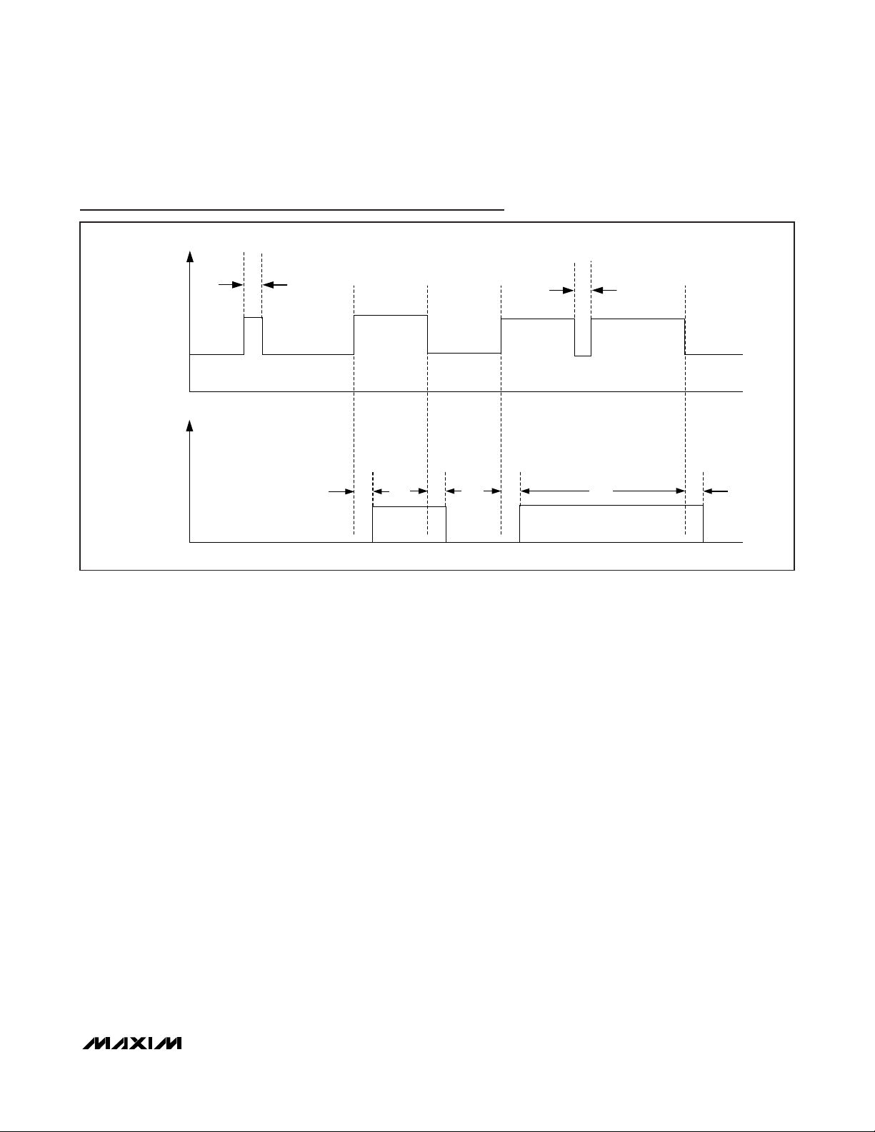
Timing Diagrams
Figure 1. Timing Diagram
APPROX. 50 mA
SHORT CIRCUIT
14mA
IN 1
7mA
RETRY
4mA/μs
0mA
5V
OUT1
0V
5V
OUT2
0V
5V
ERR
0V
5V
DIAG
0V
HALL SENSOR OPEN CIRCUIT
t
DEL
t
ERR
t
ERR
MAX9921
Dual, 2-Wire Hall-Effect Sensor Interface
with Diagnostics
_______________________________________________________________________________________ 5
Timing Diagrams (continued)
Figure 2. Hall Input Pulse Rejection
P
R
14mA
IN_
7mA
0mA
5V
OUT_
0V
P
R
t
DEL
t
DEL

MAX9921
Dual, 2-Wire Hall-Effect Sensor Interface
with Diagnostics
6 _______________________________________________________________________________________
Typical Operating Characteristics
(V
BAT
= 14V, TA= +25°C, unless otherwise noted.)
BAT SUPPLY CURRENT
vs. V
BAT
IN OPERATING MODE
BAT VOLTAGE (V)
BAT CURRENT (mA)
MAX9921 toc01
19.0 19.5 20.0 20.5 21.0
0.6
0.7
0.8
0.9
1.0
1.1
1.2
1.3
1.4
TA = -40°C
BAT SUPPLY CURRENT
vs. V
BAT
IN OPERATING MODE
BAT VOLTAGE (V)
BAT CURRENT (mA)
MAX9921 toc02
19.0 19.5 20.0 20.5 21.0
0.6
0.7
0.8
0.9
1.0
1.1
1.2
1.3
1.4
TA = +25°C
BAT SUPPLY CURRENT
vs. V
BAT
IN OPERATING MODE
BAT VOLTAGE (V)
BAT CURRENT (mA)
MAX9921 toc03
19.0 19.5 20.0 20.5 21.0
0.8
0.9
1.0
1.1
1.2
1.3
1.4
1.5
1.6
TA = +125°C
BAT SUPPLY CURRENT
vs. V
BAT
IN OPERATING MODE
BAT VOLTAGE (V)
BAT CURRENT (mA)
MAX9921 toc04
5 1015202530354045505560
0.6
0.7
0.8
0.9
1.0
1.1
1.2
1.3
TA = -40°C
HALL INPUTS DISABLED
OPERATING MODE
BAT SUPPLY CURRENT
vs. V
BAT
IN OPERATING MODE
BAT VOLTAGE (V)
BAT CURRENT (mA)
MAX9921 toc05
5 1015202530354045505560
0.6
0.7
0.8
0.9
1.0
1.1
1.2
1.3
TA = +25°C
HALL INPUTS DISABLED
OPERATING MODE
BAT SUPPLY CURRENT
vs. V
BAT
IN OPERATING MODE
BAT VOLTAGE (V)
BAT CURRENT (mA)
MAX9921 toc06
5 1015202530354045505560
0.6
0.8
1.0
1.2
1.4
1.6
HALL INPUTS DISABLED
OPERATING MODE
TA = +125°C
BAT SUPPLY CURRENT
vs. V
BAT
IN SHUTDOWN MODE
BAT VOLTAGE (V)
BAT CURRENT (nA)
MAX9921 toc07
0 10203040
0
5
10
15
20
25
30
35
40
45
50
TA = +25°C
TA = +125°C
TA= -40°C
HALL INPUT CURRENT HYSTERESIS FOR
HIGH/LOW THRESHOLDS
vs. TEMPERATURE
HALL INPUT CURRENT (mA)
MAX9921 toc08
-40 -25 -10 5 20 35 50 65 80 95 110 125
8.4
8.6
8.8
9.0
9.2
9.4
9.6
9.8
10.0
LOW THRESHOLD
HIGH THRESHOLD
HALL INPUT CURRENT HYSTERESIS FOR
HIGH/LOW THRESHOLD vs. V
BAT
BAT VOLTAGE (V)
HALL INPUT CURRENT (mA)
MAX9921 toc09
6 8 10 12 14 16 18
8.6
8.8
9.0
9.2
9.4
9.6
9.8
LOW THRESHOLD
HIGH THRESHOLD

MAX9921
Dual, 2-Wire Hall-Effect Sensor Interface
with Diagnostics
_______________________________________________________________________________________
7
Typical Operating Characteristics (continued)
(V
BAT
= 14V, TA= +25°C, unless otherwise noted.)
IN_ BLANKING TIME AT HALL SWITCH
POWER-UP vs. TEMPERATURE
TEMPERATURE (°C)
IN_ BLANKING TIME (μs)
MAX9921 toc10
-40 -25 -10 5 20 35 50 65 80 95 110 125
60
65
70
75
80
85
90
95
100
IN_ CURRENT RAMP RATE AFTER
TURN-ON vs. TEMPERATURE
TEMPERATURE (°C)
IN_ CURRENT RAMP RATE (mA/μs)
MAX9921 toc11
-40 -25 -10 5 20 35 50 65 80 95 110 125
0
1
2
3
4
5
DELAY FROM IN_ TO OUT_ (FILTER DELAY)
vs. TEMPERATURE
TEMPERATURE (°C)
DELAY (μs)
MAX9921 toc12
-40 -25 -10 5 20 35 50 65 80 95 110 125
5
6
7
8
9
10
DELAY FROM IN_ FAULT TO ERR
(FILTER DELAY) vs. TEMPERATURE
TEMPERATURE (°C)
DELAY (μs)
MAX9921 toc13
-40 -25 -10 5 20 35 50 65 80 95 110 125
0
10
20
30
40
50
DELAY DIFFERENCE BETWEEN RISING
AND FALLING EDGES FOR BOTH CHANNELS
vs. TEMPERATURE
TEMPERATURE (°C)
DELAY DIFFERENCE (ns)
MAX9921 toc14
-40 -25 -10 5 20 35 50 65 80 95 110 125
0
20
40
60
80
100
120
140
160
180
IN1 AND IN2
DELAY DIFFERENCE BETWEEN
CHANNELS vs. TEMPERATURE
TEMPERATURE (°C)
DELAY DIFFERENCE (ns)
MAX9921 toc15
-40 -25 -10 5 20 35 50 65 80 95 110 125
0
50
100
150
200
250
MAXIMUM FREQUENCY ON HALL INPUTS
vs. TEMPERATURE
TEMPERATURE (°C)
FREQUENCY (kHz)
MAX9921 toc16
-40 -25 -10 5 20 35 50 65 80 95 110 125
50
55
60
65
70
75
80
85
90
95
100
IN1 AND IN2, 50% DUTY CYCLE
IN_ PULSE LENGTH REJECTED BY FILTER
TO OUT_ vs. TEMPERATURE
TEMPERATURE (°C)
PULSE LENGTH (μs)
MAX9921 toc17
-40 -25 -10 5 20 35 50 65 80 95 110 125
0
1
2
3
4
5
6
7
IN1 AND IN2 WITH
NEGATIVE PULSE
IN1 AND IN2 WITH
POSITIVE PULSE
V
BAT
UNDERVOLTAGE THRESHOLD
vs. TEMPERATURE
TEMPERATURE (°C)
V
BAT
THRESHOLD (V)
MAX9921 toc18
-40 -25 -10 5 20 35 50 65 80 95 110 125
5.2
5.3
5.4
5.5
5.6
5.7
5.8
5.9
6.0
6.1
6.2
V
BAT
RISING, ERR GOES HIGH
V
BAT
FALLING, ERR GOES LOW
MAX9921
Dual, 2-Wire Hall-Effect Sensor Interface
with Diagnostics
8 _______________________________________________________________________________________
Typical Operating Characteristics (continued)
(V
BAT
= 14V, TA= +25°C, unless otherwise noted.)
V
BAT
OVERVOLTAGE THRESHOLD
vs. TEMPERATURE
TEMPERATURE (°C)
V
BAT
THRESHOLD (V)
MAX9921 toc19
-40 -25 -10 5 20 35 50 65 80 95 110 125
19.5
19.6
19.7
19.8
19.9
20.0
20.1
20.2
20.3
20.4
20.5
V
BAT
FALLING, ERR GOES LOW
V
BAT
RISING, ERR GOES HIGH
INPUT PULLUP RESISTANCE
vs. V
BAT
V
BAT
(V)
INPUT PULLUP RESISTANCE (Ω)
MAX9921 toc20
6 9 12 15 18
0
10
20
30
40
50
60
70
80
TA = +125°C
TA = +25°C
TA = -40°C
THRESHOLD CURRENT vs. ISET RESISTOR
CHANGE IN ISET RESISTOR (%)
CHANGE IN THRESHOLD CURRENT (%)
MAX9921 toc21
-15 -10 -5 0 5 10 15
-15
-10
-5
0
5
10
15
HYSTERESIS
INPUT CURRENT FOR OUTPUT
HIGH AND INPUT CURRENT
FOR OUTPUT LOW
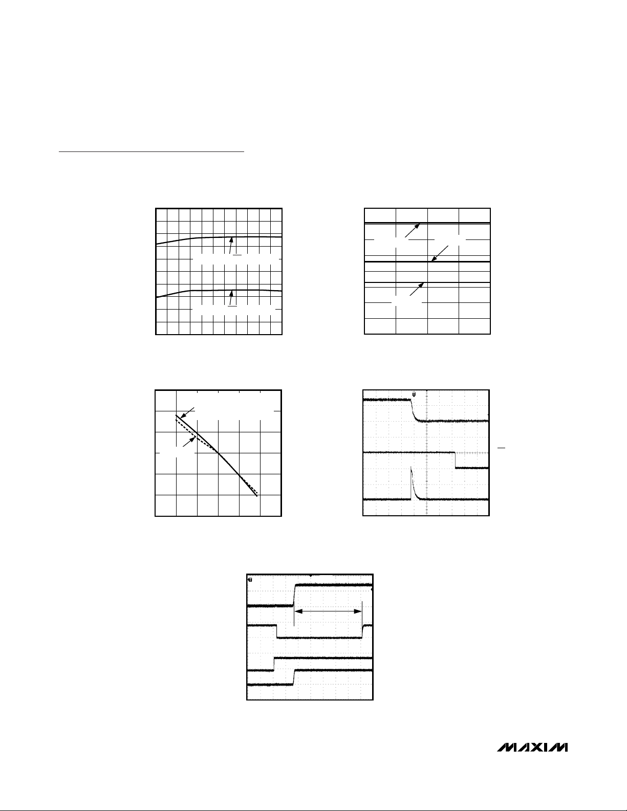
RESPONSE OF INPUT TO SHORT TO GROUND
MAX9921 toc22
10μs/div
V
IN1
10V/div
I
IN1
25mA/div
0V
0V
0A
V
ERR
5V/div
STARTUP OF HALL INPUT FROM SHUTDOWN
MAX9921 toc23
20μs/div
10V/div
5V/div
5V/div
10mA/div
BLANKING PERIOD
V
IN_
V
OUT_
V
OE_
I
IN_

MAX9921
Dual, 2-Wire Hall-Effect Sensor Interface
with Diagnostics
_______________________________________________________________________________________ 9
Pin Description
PIN NAME FUNCTION
1 BAT
2 ISET
3 IN1
4 IN2
5 GND Ground
6 OUT2
7 OUT1
8 ERR
9OE
10 DIAG
Battery Power Supply. Connect BAT to the positive supply through an external reverse-polarity diode. Bypass BAT
to ground with a 0.1µF capacitor.
Current-Setting Input. Connect a 63.4kΩ, 1% resistor (R
thresholds for Hall current sensing. Make no other connections to ISET. All routing must have low parasitic
capacitance.
Hall-Effect Sensor Input 1. Bypass IN1 to BAT or GND with a 0.01µF capacitor. Terminate an unused input with a
1.5kΩ resistor from IN1 to GND to prevent false error diagnostics.
Hall-Effect Sensor Input 2. Bypass IN2 to BAT or GND with a 0.01µF capacitor. Terminate an unused input with a
1.5kΩ resistor from IN2 to GND to prevent false error diagnostics.
Open-Drain Output Signal 2. OUT2 is the signal translated from Hall Sensor 2. Connect a 10kΩ or larger pullup
resistor to logic supply.
Open-Drain Output Signal 1. OUT1 is the signal translated from Hall Sensor 1. Connect a 10kΩ or larger pullup
resistor to logic supply.
Open-Drain Diagnostic and Error Output. Connect a 10kΩ or larger pullup resistor to logic supply. If DIAG is
asserted low, a high on ERR indicates that there is no fault while a low on ERR indicates that either the battery
voltage is out of range or there is a fault condition. If DIAG is high, ERR provides diagnostic information in
conjunction with OUT1 and OUT2. See Tables 1 and 2. If OE is low or while in shutdown, ERR is high impedance.
Output Enable Input. OE has an internal 80kΩ resistor to GND. Drive OE high to enable the outputs ERR, OUT1,
and OUT2. Drive OE low to place the outputs in high impedance. If OE and DIAG are both low for more than 40µs,
the device enters shutdown and all outputs are in high impedance. While in shutdown, if either OE or DIAG
transitions low to high, the device exits shutdown mode.
Diagnostic Enable Input. DIAG has an internal 80kΩ resistor to GND. Drive DIAG low for normal operation. In this
mode, ERR, OUT1, and OUT2 provide Hall sensor information. Drive DIAG high for diagnostic operation. A high-tolow transition initiates an attempt to restart, with a blanking cycle any Hall input that has been shut down. See
Tables 1 and 2 (diagnostic truth tables). If OE and DIAG are both low for more than 40µs, the device enters
shutdown mode with all outputs in high impedance. While in the shutdown mode, if either OE or DIAG transitions
low to high, the device exits shutdown mode.
) between BAT and ISET to set the standard current
ISET

Detailed Description
The MAX9921 connects two 2-wire Hall-effect sensors to
a low-voltage µP. This device supplies current through
IN1 and IN2 to Hall sensors and monitors the current
level drawn by the Hall sensors. The MAX9921 outputs a
high or low logic-level to the corresponding open-drain
output (OUT1 or OUT2). If the current flowing out of
either IN1 or IN2 exceeds the high input current threshold, the corresponding output goes high. If the current
flowing out of either IN1 or IN2 is lower than the low input
current threshold, the corresponding output goes low.
Hall Input Diagnostic
Normal Mode
In normal mode, DIAG is driven low. In this case, if ERR
is high, the outputs (OUT1 and OUT2) indicate the high
or low state of the corresponding Hall sensors (IN1 and
IN2). In normal mode, a low ERR indicates a fault. If
ERR is low, the outputs may be pulled low and may not
indicate the high or low state of the Hall sensors. This
can happen during the power-up, restart, or blanking
cycles of the Hall inputs, or due to a fault on one or
both of the Hall inputs, or when V
BAT
is out of range,
while the error output is low. If one output continues
signaling and the other output is low, the output with
the low logic-level indicates a fault or a restart and
blanking cycle on the corresponding Hall input. Table 1
summarizes normal mode operation.
Diagnostic Mode
When DIAG is driven high, the MAX9921 enters diagnostic mode. In this mode, OUT1 and OUT2 output diagnostic information. IN1 takes precedence over IN2. IN2’s
diagnostics remain masked until a fault on IN1 is cleared.
For diagnostics and troubleshooting, when IN1 or IN2
shuts off due to an input short to ground, it continues to
source 50µA. A falling edge at DIAG restarts a Hall input
that has been shut off due to a short to ground.
Diagnostic indications are never latched internally and
they indicate the real-time state of IN1 or IN2. Table 2
summarizes diagnostic mode operation.
Hall Input Fault Detection
If a fault is detected, the ERR output is asserted low to
notify the µP. This condition can occur due to the Hall
input being shorted to ground, shorted to battery,
or open.
MAX9921
Dual, 2-Wire Hall-Effect Sensor Interface
with Diagnostics
10 ______________________________________________________________________________________
Functional Diagram
Table 1. Diagnostic Truth Table (Normal Mode)
BAT
ISET
REF
GENERATION,
DIAGNOSTICS,
IN1
IN2
AND
OVERVOLTAGE
DETECT
FILTER
FILTER
GND
CONTROL
MAX9921
DIAG
ERR
OE
OUT1
OUT2
INPUT OUTPUT
DIAG ERR OUT1 OUT2
0 1 0 or 1 0 or 1
00 0 0
0 0 0 0 or 1 Fault on IN1 or restart blanking of IN1
0 0 0 or 1 0 Fault on IN2 or restart blanking of IN2
OUT1 and OUT2 indicate state of IN1
and IN2, respectively
Fault on IN1 and/or IN2, or V
of range, or power-up or restart
blanking (unknown current level of
IN1 and IN2)
DIAGNOSIS COMMENT
Normal mode: No fault indication (outputs
indicate Hall sensor high or low status)
out
BAT
Normal mode: ERR asserted low indicates
fault (outputs may no longer indicate the
high or low state of the Hall sensors)
Normal mode: ERR asserted low indicates
fault; Hall output 2 continues signaling
Normal mode: ERR asserted low indicates
fault; Hall output 1 continues signaling
MAX9921
Dual, 2-Wire Hall-Effect Sensor Interface
with Diagnostics
______________________________________________________________________________________ 11
Hall Sensor Protection from Supply Transients
If the V
BAT
voltage is lower than 6V or exceeds 18V,
IN1 and IN2 shut off current to both Hall sensors and
ERR, OUT1, and OUT2 go low. When V
BAT
returns to
the proper range, both IN1 and IN2 restart, following a
blanking cycle.
Hall Inputs Open Condition
If either IN1 or IN2 is open (IIN< 2mA), the corresponding input shuts off current to the Hall sensor. If IN1 or
IN2 is loaded, it exits the open input fault condition and
restarts the corresponding Hall input, following a blanking cycle.
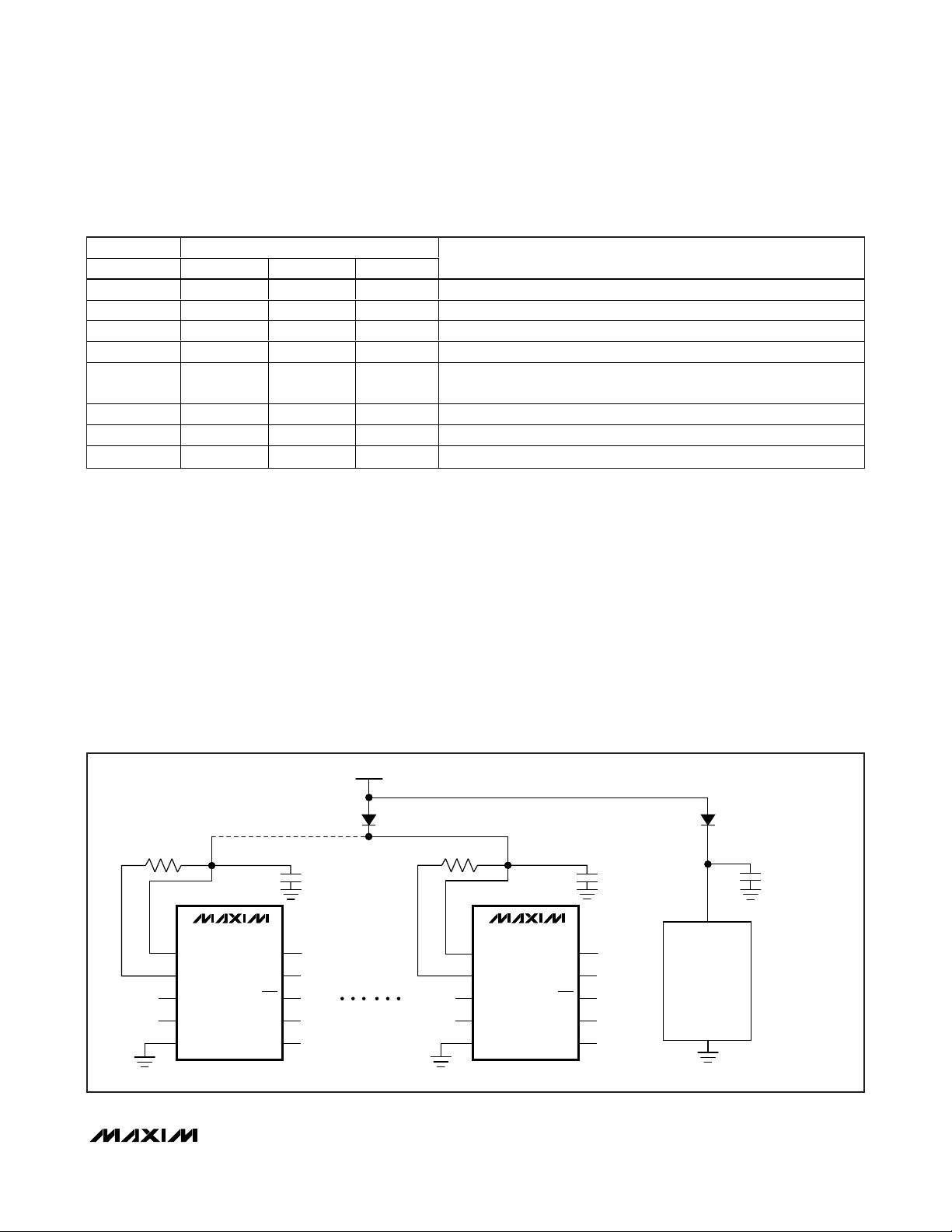
Hall Input Shorted to Battery
If either IN1 or IN2 is shorted to the battery (VIN> V
BAT
+ 100mV), the MAX9921 shuts off current to the corresponding Hall sensor. In this case, if IN1 or IN2 is more
than 1V above V
BAT
, it may back-drive current into
BAT. In such a condition, the current level in the Hall
input should not exceed 100mA. Therefore, all the
MAX9921s together can share a separate reversepolarity protection diode to avoid powering up other circuitry sharing a common diode (Figure 4).
Table 2. Diagnostic Truth Table (Diagnostic Mode)
Figure 4. Several MAX9921s Connected to a Common Reverse-Polarity Diode
INPUT OUTPUT
DIAG ERR OUT1 OUT2
1 0 0 0 No fault
1 0 0 1 IN1 open circuit, or IN1 open circuit and fault on IN2
1 0 1 0 IN1 shorted to battery, or IN1 shorted to battery and fault on IN2
1 0 1 1 IN1 shorted to ground, or IN1 shorted to ground and fault on IN2
V
out of range, or power-up or restart and blanking cycle (dominant
1100
1 1 0 1 IN2 open circuit
1 1 1 0 IN2 shorted to battery
1 1 1 1 IN2 shorted to ground
BAT
fault masks all other faults)
DIAGNOSIS
BATTERY
REVERSE-POLARITY DIODE
R
ISET
MAX9921
BAT
ISET
IN1
IN2
GND
DIAG
OE
ERR
OUT1
OUT2
FOR MAX9921s
R
ISET
MAX9921
BAT
ISET
IN1
IN2
GND
DIAG
ERR
OUT1
OUT2
REVERSE-POLARITY DIODE
FOR OTHER CIRCUITRY
BAT
OE
OTHER
CIRCUITRY
GND

MAX9921
Hall Input Short-to-Ground
The Hall input shorted-to-ground fault is effectively a
latched condition if the input remains loaded by the Hall
switch when the shorting condition is removed. The current required to power the Hall switch is shut off and only
a 50µA pullup current remains. The Hall input can be
manually re-energized or it can be re-energized by the
ECU. A falling edge at DIAG initiates a restart with a
blanking cycle of any Hall input that has been shut down
due to the shorted-to-ground condition. During startup or
restart, it is possible for a Hall input to charge up an external capacitance of 0.02µF without tripping into a shortedto-ground latched state. All other fault conditions are not
latched and when these other faults are removed, ERR
goes high and the Hall input is again functional.
Manual Method for Re-Energizing Hall Sensor
and Means for Diagnosing an Intermittent
Hall Sensor Connection
Figure 5 shows the behavior of the MAX9921 when a
Hall input is open. Figure 6 shows the behavior of the
MAX9921 when the open input is reconnected to a Hall
sensor. Figures 5 and 6 demonstrate how a shorted-toground Hall input can be reset.
Resetting a shorted-to-ground Hall input involves
three steps:
1) Relieve the short to ground at the Hall sensor.
2) Disconnect the Hall input from the Hall sensor (open
input fault condition).
3) Reconnect the Hall input to the Hall sensor.
The MAX9921 restarts the Hall input with a blanking
cycle. If the Hall input is disconnected from the Hall
sensor for 10ms, it allows the Hall input to be pulled up
by the 50µA pullup current to register the open-input
fault condition. Then, reconnecting the Hall input to the
Hall sensor restarts the Hall input with a blanking cycle.
This provides a manual means of re-energizing a Hall
input without having to resort to the ECU to reset it. This
also demonstrates that an intermittent connection to a
Hall sensor can recover without intervention of the ECU.
This gives the ECU a means of diagnosing an intermittent connection to a Hall sensor by using the diagnostic
mode to detect a diagnostic sequence of “open-circuit”
to “blanking cycle” to “no fault.”
Dual, 2-Wire Hall-Effect Sensor Interface
with Diagnostics
12 ______________________________________________________________________________________
Figure 5. Hall Input Ramps to Open-Circuit Fault When Short to Ground is Relieved
14V
V
IN_
DISCONNECTED
0V
I
IN_
50μA
0A
HALL INPUT
SHORT TO
GROUND FAULT
INDICATED
5mV/ms
HALL INPUT
FROM SENSOR
HALL INPUT
OPEN-CIRCUIT
FAULT INDICATED
V
BAT
- 25mV
TIME
TIME

MAX9921
Dual, 2-Wire Hall-Effect Sensor Interface
with Diagnostics
______________________________________________________________________________________ 13
V
Figure 6. Hall Input Re-Energized When Open Input is Reconnected to Hall Sensor
Table 3. Summary of Fault Protection and Recovery
IN_
11.5mA
I
IN_
14V
V
- 500mV
8V
HALL INPUT
RECONNECTED
TO HALL SENSOR
0V
4mA/μs
BAT
TIME
0A
FAULT
DESCRIPTION
V
< 6V — Asserted low
BAT
V
> 18V — Asserted low
BAT
Hall input open IIN < 2mA Asserted low
Hall input shorted
to battery
Hall input shorted
to ground
CRITERION
V
> V
IN
to external
reverse-battery
protection
I
IN
due
BAT
Asserted low
diode
> 23mA Asserted low
OUTPUT
MAX9921 ACTIONS
ERR
Shutoff current to both Hall
sensors
Shutoff current to both Hall
sensors
Shutoff current to
corresponding Hall sensor
Shutoff current to
corresponding Hall sensor
Shutoff current to
corresponding Hall sensor.
50µA of pullup current is
sourced to IN1 or IN2 to
aid in troubleshooting.
HALL INPUT RESPONSE
TIME
COMMENT/RECOVERY
Both IN1 and IN2 are restarted with blanking
cycle when V
Both IN1 and IN2 are restarted with blanking
cycle when V
When a Hall input is again loaded, terminating
open input condition, the Hall input are restarted
with blanking cycle.
If a Hall input is pulled more than 1V above
V
, the input may back drive current into the
BAT
BAT supply and pull V
condition, current levels in the Hall inputs should
never exceed 100mA. For this reason, it is
recommended that one or more MAX9921s be
powered together and share a reverse-polarity
diode separate from other circuitry.
A falling edge at DIAG initiates a restart with a
blanking cycle of any Hall input that has been
shut off due to a short to ground. See Hall input
short-to-ground description.
returns to proper range.
BAT
returns to proper range.
BAT
up with it. In this
BAT
MAX9921
Dual, 2-Wire Hall-Effect Sensor Interface
with Diagnostics
14 ______________________________________________________________________________________
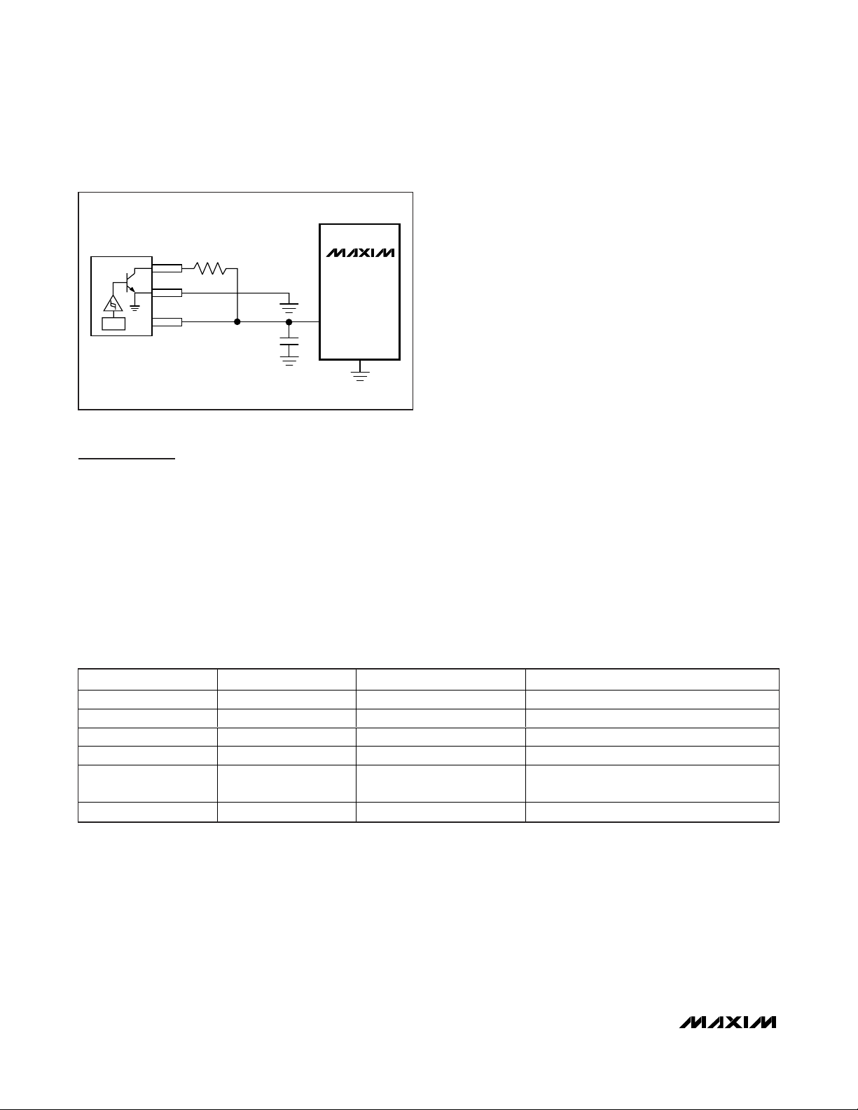
Applications Information
Hall-Effect Sensor Selection
The MAX9921 is optimized for use with 2-wire Halleffect switches or with 3-wire Hall-effect switches connected as 2-wire (Figure 7). When using a 3-wire Hall
sensor, the resistor R is chosen so that the current
drawn by the Hall sensor crosses the MAX9921 current
threshold when the magnetic threshold of the Hall sensor is exceeded.
Table 4 shows a partial list of mostly 2-wire Hall switches, which can be used with the MAX9921.
Hall Input Bypass Capacitor
The MAX9921 is optimized for use with external protection 0.01µF capacitors from both IN1 and IN2 to BAT.
These are essential to ensure robustness against automotive transients. These capacitors may be tied to
GND instead of to BAT, but the connection to BAT is
recommended.
Low-Voltage Operation
To ensure correct operation of the Hall sensor at low
input voltages, it is important to consider the voltage
drop of the MAX9921 with low battery voltages. This
dropout voltage can be calculated using the formula:
V
DROPOUT
= I
HALL
x R
PU
I
HALL
is the maximum current which must be supplied to
the Hall sensor and RPUis the internal resistance of the
MAX9921, nominally 50Ω (see the Input Pullup
Resistance vs. V
BAT
graph in the
Typical Operating
Characteristics
). As an example, assume the use of a
HAL573 sensor, which draws a maximum current of
17mA. The dropout voltage is then 850mV and the
approximate minimum voltage supplied to the Hall sensor
is 6V - 0.85V = 5.15V, which is higher than the minimum
operating voltage of 3.75V specified for the HAL573.
Figure 7. 3-Wire Hall-Effect Switches Configured as 2-Wire
Table 4. Partial List of Compatible Hall Switches
R
V
CC
x_
MAX9921
IN_
GND
PART MANUFACTURER WEBSITE COMMENT
HAL573-6 Micronas www.micronas.com 2-wire
HAL556/560/566 Micronas www.micronas.com 2-wire
HAL581/584 Micronas www.micronas.com 2-wire
A1140/1/2/3 Allegro www.allegromicro.com 2-wire
3161 Allegro www.allegromicro.com
TLE4941/C Infineon www.infineon.com 2-wire
3-wire, optimized for 2-wire use without added
resistor

MAX9921
Dual, 2-Wire Hall-Effect Sensor Interface
with Diagnostics
Maxim cannot assume responsibility for use of any circuitry other than circuitry entirely embodied in a Maxim product. No circuit patent licenses are
implied. Maxim reserves the right to change the circuitry and specifications without notice at any time.
Maxim Integrated Products, 120 San Gabriel Drive, Sunnyvale, CA 94086 408-737-7600 ____________________
15
© 2008 Maxim Integrated Products is a registered trademark of Maxim Integrated Products, Inc.
Chip Information
PROCESS: BiCMOS
Pin Configuration
PACKAGE TYPE PACKAGE CODE DOCUMENT NO.
10 µMAX U10+2
21-0061
Package Information
For the latest package outline information and land patterns, go
to www.maxim-ic.com/packages
.
TOP VIEW
BAT
ISET
IN1
DIAG
1
2
3
MAX9921
4
5
μMAX
10
OE
9
ERR
8
OUT1IN2
7
6
OUT2GND
 Loading...