

Page 1

General Description
The single MAX9910/MAX9911 and dual MAX9912/
MAX9913 operational amplifiers (op amps) feature a
maximized ratio of gain bandwidth (GBW) to supply
current and are ideal for battery-powered applications
such as portable instrumentation, portable medical
equipment, and wireless handsets. These CMOS op
amps feature an ultra-low input-bias current of 1pA, railto-rail inputs and outputs, low supply current of 4µA,
and operate from a single 1.8V to 5.5V supply. For
additional power conservation, the MAX9911/MAX9913
feature a low-power shutdown mode that reduces supply current to 1nA, and puts the amplifiers’ outputs in a
high-impedance state. These devices are unity-gain
stable with a 200kHz GBW product.
The MAX9910 is available in a 5-pin SC70 package. The
MAX9911 is available in tiny 6-bump WLP and a 6-pin
SC70 packages. The MAX9912 is available in an 8-pin
SOT23 package, and the MAX9913 is available in a 10pin µMAX®package. All devices are specified over the
-40°C to +85°C extended operating temperature range.
Applications
Portable Medical Devices
Portable Test Equipment
Laptops
Data-Acquisition Equipment
Features
o 200kHz GBW
o Ultra-Low 4µA Supply Current
o Single 1.8V to 5.5V Supply Voltage Range
o Ultra-Low 1pA Input Bias Current
o Rail-to-Rail Input and Output Voltage Ranges
o Low ±200µV Input Offset Voltage
o Low 0.001µA Shutdown Current
o High-Impedance Output During Shutdown
(MAX9911/MAX9913)
o Unity-Gain Stable
o Available in Tiny WLP, SC70, SOT23, and µMAX
Packages
MAX9910–MAX9913
200kHz, 4µA, Rail-to-Rail
I/O Op Amps with Shutdown
________________________________________________________________
Maxim Integrated Products
1
19-3406; Rev 2; 10/10
For pricing, delivery, and ordering information, please contact Maxim Direct at 1-888-629-4642,
or visit Maxim’s website at www.mxim-ic.com.
Ordering Information
Typical Operating Circuit
Selector Guide
+
Denotes lead(Pb)-free/RoHS-compliant package.
µMAX is a registered trademark of Maxim Integrated Products, Inc.
1.8V TO 5.5V
OUTA
INA-
INA+
V
MID
OUTB
INB-
V
DD
V
OUT
25kΩ
PART TEMP RANGE
MAX9910EXK+T -40°C to +85°C 5 SC70 AGA
MAX9910EXK-T -40°C to +85°C 5 SC70 AGA
MAX9911EXT+T -40°C to +85°C 6 SC70 ACA
MAX9911EXT-T -40°C to +85°C 6 SC70 ACA
MAX9911EWT+ -40°C to +85°C 6 WLP BQ
MAX9912EKA+T -40°C to +85°C 8 SOT23 AEJY
MAX9912EKA-T -40°C to +85°C 8 SOT23 AEJY
MAX9913EUB -40°C to +85°C 10 µMAX —
MAX9913EUB+ -40°C to +85°C 10 µMAX —
PINPACKAGE
TOP
MARK
INB+
V
+ V
MID
V
SS
ON
SHDNA
OFF
1MΩ
THREE ELECTRODE GLUCOSE METER APPLICATION WITH SHUTDOWN
MAX9913
CE
RE
GLUCOSE
SENSOR
WE
SHDNB
BIAS
ON
OFF
PART
MAX9910EXK-T 1 No
MAX9911EXT-T 1 Yes
MAX9912EKA-T 2 No
MAX9913EUB 2 Yes
AMPLIFIERS
PER PACKAGE
SHUTDOWN
MODE
Page 2
MAX9910–MAX9913
200kHz, 4µA, Rail-to-Rail
I/O Op Amps with Shutdown
2 _______________________________________________________________________________________
ABSOLUTE MAXIMUM RATINGS
Stresses beyond those listed under “Absolute Maximum Ratings” may cause permanent damage to the device. These are stress ratings only, and functional
operation of the device at these or any other conditions beyond those indicated in the operational sections of the specifications is not implied. Exposure to
absolute maximum rating conditions for extended periods may affect device reliability.
Power-Supply Voltage (VDDto VSS) ......................-0.3V to +6.0V
IN_+, IN_-, OUT_, SHDN_ ............... (V
SS
- 0.3V) to (VDD+ 0.3V)
Current into IN_+, IN_- ......................................................±20mA
Output Short-Circuit Duration to V
DD
or VSS..............Continuous
Continuous Power Dissipation (T
A
= +70°C)
5-Pin SC70 (derate 3.1mW/°C above +70°C)............. 247mW
6-Bump WLP (derate 10.5mW/°C above +70°C).........840mW
6-Pin SC70 (derate 3.1mW/°C above +70°C)............. 245mW
8-Pin SOT23 (derate 9.1mW/°C above +70°C)........... 727mW
10-Pin µMAX (derate 5.6mW/°C above +70°C) ...........444mW
Operating Temperature Range .......................... -40°C to +85°C
Junction Temperature .....................................................+150°C
Storage Temperature Range ............................-65°C to +150°C
Lead Temperature (excluding WLP, soldering 10s) ........+300°C
Soldering Temperature (reflow)
Lead(Pb)-Free Packages.............................................+260°C
Packages Containing Lead(Pb)...................................+240°C
ELECTRICAL CHARACTERISTICS
(VDD= 1.8V to 5.5V, VSS= 0V, VCM= 0V, V
OUT
= VDD/ 2, RL= ∞ connected to VDD/ 2, SHDN_ = VDD, TA= +25°C, unless otherwise
noted.) (Note 1)
)
Supply Voltage Range V
PARAMETER SYMBOL CONDITIONS MIN TYP MAX UNITS
Supply Current I
Shutdown Supply Current I
Input Offset Voltage V
Input-Offset-Voltage Matching MAX9912/MAX9913 ±250 µV
Input Bias Current I
Input Offset Current I
Input Resistance R
Input Common-Mode Range V
Common-Mode Rejection Ratio CMRR -0.1V < VCM < VDD + 0.1V, VDD = 5.5V 70 80 dB
Power-Supply Rejection Ratio PSRR 1.8V < VDD < 5.5V 65 95 dB
Open-Loop Gain A
Output-Voltage-Swing High V
Channel-to-Channel Isolation CH
Output Short-Circuit Current I
DD(SHDN_
OUT(SC)
DD
DD
OS
B
OS
IN
CM
VOL
OH
OL
ISO
Guaranteed by PSRR test 1.8 5.5 V
MAX9910/MAX9911
MAX9912/MAX9913
SHDN_ = GND, MAX9911/MAX9913 0.001 0.5 µA
(Note 2) ±1 ±10 pA
(Note 2) ±1 ±10 pA
Common mode 1
Differential mode, -1mV < VIN < +1mV 10
Guaranteed by CMRR test
25mV < V
R
L
100mV < V
R
L
VDD - V
V
OUT
Specified at DC, MAX9912/MAX9913 100 dB
OUT
= 100kΩ, VDD = 5.5V
- V
OUT
OUT
SS
= 5kΩ, VDD = 5.5V
VDD = 1.8V 4
= 5.5V 4 5.0
V
DD
VDD = 1.8V 7
= 5.5V 7 9
V
DD
±0.2 ±1mV
V
< VDD - 25mV,
< VDD - 100mV,
RL = 100kΩ 2.5 5
RL = 5kΩ 50 70
RL = 1kΩ 250
RL = 100kΩ 2.5 5
RL = 5kΩ 50 70Output-Voltage-Swing Low V
RL = 1kΩ 250
-
SS
0.1
95 120
95 110
VDD +
0.1
±15 mA
µA
GΩ
V
dB
mV
mV
Page 3
MAX9910–MAX9913
200kHz, 4µA, Rail-to-Rail
I/O Op Amps with Shutdown
_______________________________________________________________________________________ 3
ELECTRICAL CHARACTERISTICS (continued)
(VDD= 1.8V to 5.5V, VSS= 0V, VCM= 0V, V
OUT
= VDD/ 2, RL= ∞ connected to VDD/ 2, SHDN_ = VDD, TA= +25°C, unless otherwise
noted.) (Note 1)
(
)
ELECTRICAL CHARACTERISTICS
(VDD= 1.8V to 5.5V, VSS= 0V, VCM= 0V, V
OUT
= VDD/2, RL= ∞ connected to VDD/ 2, SHDN_ = VDD, TA= -40°C to +85°C, unless
otherwise noted.) (Note 1)
)
SHDN_ Logic Low V
SHDN_ Logic High V
SHDN_ Input Bias Current
Output Leakage in Shutdown I
Gain-Bandwidth Product 200 kHz
Slew Rate 0.1 V/µs
Capacitive-Load Stability (See
the Driving Capacitive Loads
Section)
Input Voltage-Noise Density f = 1kHz 400 nV/√Hz
Input Current-Noise Density f = 1kHz 0.001 pA/√Hz
Settling Time To 0.1%, V
Delay Time to Shutdown t
Delay Time to Enable t
Power-Up Time VDD = 0 to 5.5V step 5 µs
PARAMETER SYMBOL CONDITIONS MIN TYP MAX UNITS
OUT
C
IL
IH
I
IL
I
IH
SHDN_
LOAD
SH
EN
VDD = 1.8V to 3.6V, MAX9911/MAX9913 0.4
VDD = 3.6V to 5.5V, MAX9911/MAX9913 0.8
VDD = 1.8V to 3.6V, MAX9911/MAX9913 1.4
VDD = 3.6V to 5.5V, MAX9911/MAX9913 2
SHDN_ = VSS, MAX9911/MAX9913 (Note 2) 1
SHDN_ = V
SHDN_ = VSS, V
MAX9911/MAX9913
No sustained
oscillations
IDD = 5% of normal operation,
= 5.5V, V
V
DD
= 2.7V, V
V
OUT
V
= 5.5V, V
DD
, MAX9911/MAX9913 500
DD
= 0V to VDD,
OUT
AV = 1V/V 30
AV = 10V/V 250
RL = 5kΩ, AV = 1V/V 200
R
= 1kΩ, AV = 1V/V 100
ISO
= 2V step, AV = -1V/V 18 µs
OUT
= 5.5V to 0 step
SHDN_
settles to 0.1%,
OUT
= 0 to 5.5V step
SHDN_
1 500 nA
2µs
30 µs
V
V
nA
pF
Supply Voltage Range V
Supply Current I
Shutdown Supply Current I
Input Offset Voltage V
Input-Offset-Voltage
Temperature Coefficient
PARAMETER SYMBOL CONDITIONS MIN TYP MAX UNITS
DD(SHDN_
TC
DD
DD
OS
VOS
Guaranteed by PSRR test 1.8 5.5 V
MAX9910/MAX9911 5.5
MAX9912/MAX9913
SHDN_ = GND, MAX9911/MAX9913 1 µA
V
DD
= 5.5V
11
±5mV
±5 µV/°C
µA
Page 4
MAX9910–MAX9913
200kHz, 4µA, Rail-to-Rail
I/O Op Amps with Shutdown
4 _______________________________________________________________________________________
Note 1: Specifications are 100% tested at TA= +25°C (exceptions noted). All temperature limits are guaranteed by design.
Note 2: Guaranteed by design, not production tested.
ELECTRICAL CHARACTERISTICS (continued)
(VDD= 1.8V to 5.5V, VSS= 0V, VCM= 0V, V
OUT
= VDD/2, RL= ∞ connected to VDD/ 2, SHDN_ = VDD, TA= -40°C to +85°C, unless
otherwise noted.) (Note 1)
)
Input Bias Current I
Input Offset Current I
Input Common-Mode Range V
Common-Mode Rejection Ratio CMRR -0.05V < VCM < VDD + 0.05V, VDD = 5.5V 60 dB
Power-Supply Rejection Ratio PSRR 1.8V < VDD < 5.5V 59 dB
Open-Loop Gain A
Output-Voltage-Swing High V
PARAMETER SYMBOL CONDITIONS MIN TYP MAX UNITS
Output-Voltage-Swing Low V
SHDN_ Logic Low V
SHDN_ Logic High V
SHDN_ Input-Bias Current
Output Leakage in Shutdown I
OUT(SHDN_
B
OS
V
-
CM
VOL
OH
OL
IL
IH
I
IL
I
IH
Guaranteed by CMRR test
OUT
SS
OUT
OUT
< V
< V
OUT
- 25mV,
DD
- 150mV,
DD
RL = 100kΩ 5
RL = 5kΩ 90
RL = 100kΩ 5
RL = 5kΩ 90
= 0V to VDD,
25mV < V
= 100kΩ, VDD = 5.5V
R
L
150mV < V
= 5kΩ, VDD = 5.5V
R
L
VDD - V
V
- V
OUT
VDD = 1.8V to 3.6V 0.4
VDD = 3.6V to 5.5V 0.8
VDD = 1.8V to 3.6V, MAX9911/MAX9913 1.4
VDD = 3.6V to 5.5V, MAX9911/MAX9913 2
SHDN_ = VSS, MAX9911/MAX9913 5 nA
SHDN_ = VDD, MAX9911/MAX9913 1000 nA
SHDN_ = VSS, V
MAX9911/MAX9913
SS
0.05
85
80
±30 pA
±20 pA
VDD +
0.05
1000 nA
V
dB
mV
mV
V
V
Page 5
MAX9910–MAX9913
200kHz, 4µA, Rail-to-Rail
I/O Op Amps with Shutdown
_______________________________________________________________________________________
5
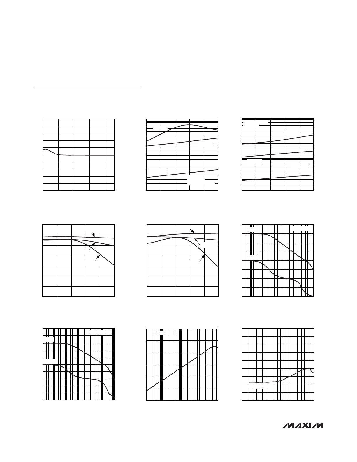
Typical Operating Characteristics
(VDD= 3V, VSS= VCM= 0V, RL to VDD/ 2, TA= +25°C, unless otherwise noted.)
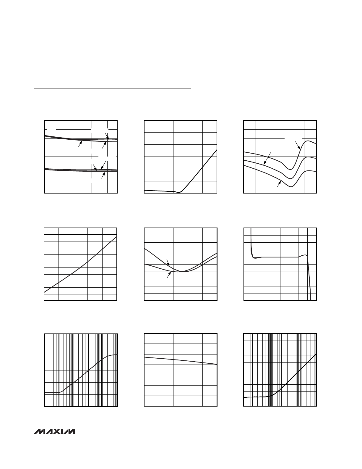
SUPPLY CURRENT
vs. SUPPLY VOLTAGE
9
8
DUAL
7
6
(µA)
5
CC
I
SINGLE
4
3
2
1
1.8 5.5
TA = +85°C
V
TA = +25°C
SUPPLY
TA = -40°C
TA = +25°C
TA = +85°C
(V)
INPUT OFFSET VOLTAGE
vs. TEMPERATURE
200
150
100
50
0
-50
(µV)
OS
-100
V
-150
-200
-250
-300
-350
-40 85
TEMPERATURE (°C)
TA = -40°C
5.04.22.6 3.4
603510-15
MAX9910 toc01
SHUTDOWN SUPPLY CURRENT (nA)
MAX9910 toc04
(pA)
I
SHUTDOWN SUPPLY CURRENT
vs. TEMPERATURE
12
10
8
6
4
2
0
-40 85
TEMPERATURE (°C)
INPUT BIAS CURRENT
vs. TEMPERATURE
7
6
5
4
3
2
B
1
0
-1
-2
-3
-40 85
IB-
IB+
TEMPERATURE (°C)
603510-15
603510-15
MAX9910 toc02
MAX9910 toc05
INPUT OFFSET VOLTAGE
vs. INPUT COMMON-MODE VOLTAGE
1000
750
500
250
(µV)
0
OS
V
-250
-500
-750
-1000
0 3.0
TA = +85°C
TA = -40°C
TA = +25°C
VCM (V)
INPUT BIAS CURRENT
vs. INPUT COMMON-MODE VOLTAGE
5
4
3
2
1
0
(pA)
B
I
-1
-2
-3
-4
-5
-0.5 3.5
VCM (V)
MAX9910 toc03
2.52.00.5 1.0 1.5
MAX9910 toc06
3.02.51.5 2.00.5 1.00
POWER-SUPPLY REJECTION RATIO
vs. FREQUENCY
0
-20
-40
-60
PSRR (dB)
-80
-100
-120
0.1 10k
FREQUENCY (Hz)
COMMON-MODE REJECTION RATIO
vs. TEMPERATURE
140
120
MAX9910 toc07
100
80
60
CMRR (dB)
40
20
0
1k100101
-40 85
TEMPERATURE (°C)
603510-15
MAX9910 toc08
COMMON-MODE REJECTION RATIO
vs. FREQUENCY
0
-10
-20
-30
-40
-50
CMRR (dB)
-60
-70
-80
-90
-100
FREQUENCY (Hz)
MAX9910 toc09
10k1k100101100k
Page 6
MAX9910–MAX9913
200kHz, 4µA, Rail-to-Rail
I/O Op Amps with Shutdown
6 _______________________________________________________________________________________
Typical Operating Characteristics (continued)
(VDD= 3V, VSS= VCM= 0V, RL to VDD/ 2, TA= +25°C, unless otherwise noted.)
SLEW RATE
vs. SUPPLY VOLTAGE
0.6
0.5
0.4
0.3
0.2
0.1
0
SLEW RATE (V/µS)
-0.1
-0.2
-0.3
-0.4
1.8 5.5
SUPPLY VOLTAGE (V)
MAX9910 toc10
5.04.23.42.6
1000
100
10
OUTPUT VOLTAGE SWING (mV)
OPEN-LOOP GAIN
RL = 100k
RL = 5k
L
Ω
RL = 1k
TO VSS)
Ω
Ω
603510-15-40 85
MAX9910 toc13
(dB)
VOL
A
140
120
100
80
60
40
20
(dB)
VOL
A
vs. TEMPERATURE (R
140
120
100
80
60
40
20
0
TEMPERATURE (°C)
OUTPUT-SWING HIGH
vs. TEMPERATURE
Ω
RL = 1k
Ω
RL = 5k
Ω
RL = 100k
RL TO V
SS
VOH = VDD - V
1
-40 85
TEMPERATURE (°C)
OUT
603510-15
OPEN-LOOP GAIN
Ω
RL = 1k
TO VDD)
L
RL = 5k
Ω
603510-15-40 85
Ω
vs. TEMPERATURE (R
RL = 100k
0
TEMPERATURE (°C)
10000
VOL = V
MAX9910 toc11
RL TO V
1000
100
RL = 5k
10
OUTPUT VOLTAGE SWING (mV)
1
-40 85
vs. FREQUENCY (R
80
GAIN
60
MAX9910 toc14
40
20
PHASE
0
GAIN (dB)
-20
-40
-60
-80
11M
OUTPUT-SWING LOW
vs. TEMPERATURE
- V
OUT
SS
DD
Ω
TEMPERATURE (°C)
RL = 1k
GAIN AND PHASE
= ∞, C
L
FREQUENCY (Hz)
Ω
RL = 100k
603510-15
= 15pF)
LOAD
MAX9910 toc15
AV = 1000V/V
100k10k10 100 1k
MAX9910 toc12
Ω
180
135
90
45
0
-45
PHASE (DEGREES)
-90
-135
-180
GAIN AND PHASE
vs. FREQUENCY (R
100
80
GAIN
60
40
20
PHASE
0
GAIN (dB)
-20
-40
-60
-80
-100
11M
= 5kΩ, C
L
FREQUENCY (Hz)
= 100pF)
LOAD
MAX9910 toc16
AV = 1000V/V
100k10k10 100 1k
225
180
135
90
45
0
-45
PHASE (DEGREES)
-90
-135
-180
-225
0
MAX9912/MAX9913
-20
-40
-60
CROSSTALK (dB)
-80
-100
-120
10 100k
CROSSTALK
vs. FREQUENCY
MAX9910 toc17
THD+N (dB)
10k1k100
FREQUENCY (Hz)
TOTAL HARMONIC DISTORTION
PLUS NOISE vs. FREQUENCY
-5
-15
-25
-35
-45
-55
-65
-75
V
= 2V
OUT
P-P
-85
-95
10 10k
FREQUENCY (Hz)
MAX9910 toc18
1k100
Page 7

MAX9910–MAX9913
200kHz, 4µA, Rail-to-Rail
I/O Op Amps with Shutdown
_______________________________________________________________________________________
7
Typical Operating Characteristics (continued)
(VDD= 3V, VSS= VCM= 0V, RL to VDD/ 2, TA= +25°C, unless otherwise noted.)
POWER-UP SETTLING TIME
MAX9910 toc21
500ns/div
OUTPUT
500mV/div
V
DD
1V/div
IN+ = VDD / 2
A
V
= 1V/V
VOLTAGE-NOISE DENSITY
vs. FREQUENCY
10,000
MAX9910 toc19
1000
VOLTAGE NOISE (nV/√Hz)
100
SHDN
OUTPUT
10 100 1k 10k
1100k
FREQUENCY (Hz)
SHUTDOWN RESPONSE
MAX9910 toc22
IN+ = VDD / 2
= 1V/V
A
V
3V
0V
1.5V
0V
8000
7000
6000
5000
(Ω)
4000
ISO
R
3000
2000
1000
0
10 10,000
IN+
50mV/div
OUTPUT
50mV/div
RESISTOR ISOLATION
vs. CAPACITIVE LOAD
AV = 1V/V
= 10V/V
FOR A
V
NEEDED
NO R
ISO
1000100
C
(pF)
LOAD
SMALL-SIGNAL PULSE RESPONSE
= 15pF)
(C
LOAD
MAX9910 toc23
AV = 1V/V
MAX9910 toc20
IN+
5mV/div
OUTPUT
50mV/div
SMALL-SIGNAL PULSE RESPONSE
= 100pF)
(C
LOAD
MAX9910 toc24
AV = 10V/V
20µs/div
LARGE-SIGNAL PULSE RESPONSE
= 15pF)
(C
LOAD
IN+
1V/div
OUTPUT
1V/div
10µs/div
MAX9910 toc25
AV = 1V/V
10µs/div
IN+
100mV/div
OUTPUT
1V/div
LARGE-SIGNAL PULSE RESPONSE
= 100pF)
(C
LOAD
100µs/div
20µs/div
MAX9910 toc26
AV = 10V/V
Page 8

MAX9910–MAX9913
200kHz, 4µA, Rail-to-Rail
I/O Op Amps with Shutdown
8 _______________________________________________________________________________________
Typical Operating Characteristics (continued)
(VDD= 3V, VSS= VCM= 0V, RL to VDD/ 2, TA= +25°C, unless otherwise noted.)
PERCENT OVERSHOOT
vs. CAPACITIVE LOAD
MAX9910 toc29
C
LOAD
(pF)
OVERSHOOT (%)
806020 40
0.5
1.0
1.5
2.0
3.0
2.5
3.5
4.0
0
0100
AV = 1V/V
RL = 1M
Ω
RL = 100k
Ω
RL = 10k
Ω
OUTPUT WAVEFORM WITH R
ISO
(C
LOAD
= 100pF, R
ISO
= 6.2kΩ)
MAX9910 toc30
20µs/div
OUTPUT
50mV/div
IN+
50mV/div
AV = 1V/V
OUTPUT WAVEFORM WITHOUT R
ISO
(C
LOAD
= 100pF)
20µs/div
MAX9910 toc31
OUTPUT
50mV/div
IN+
50mV/div
AV = 1V/V
LARGE-SIGNAL GAIN
vs. FREQUENCY
FREQUENCY (kHz)
GAIN (dB)
-4
-3
-2
-1
0
2
1
4
3
MAX9910 toc28
100101
AV = +1V/V
V
OUT
= 2V
P-P
C
LOAD
= 15pF
SMALL-SIGNAL GAIN
vs. FREQUENCY
MAX9910 toc27
FREQUENCY (kHz)
GAIN (dB)
10010
-8
-6
-4
-2
0
2
4
6
8
10
-10
11000
AV = +1V/V
V
OUT
= 100mV
P-P
C
LOAD
= 15pF
Page 9

MAX9910–MAX9913
200kHz, 4µA, Rail-to-Rail
I/O Op Amps with Shutdown
_______________________________________________________________________________________ 9
Detailed Description
Featuring a maximized ratio of GBW to supply current,
low operating supply voltage, low input bias current,
and rail-to-rail inputs and outputs, the MAX9910–
MAX9913 are an excellent choice for precision or general-purpose, low-current, low-voltage, battery-powered
applications. These CMOS devices consume an ultralow 4µA (typ) supply current and a 200µV (typ) offset
voltage. For additional power conservation, the
MAX9911/MAX9913 feature a low-power shutdown
mode that reduces supply current to 1nA (typ), and
puts the amplifiers’ output in a high-impedance state.
These devices are unity-gain stable with a 200kHz
GBW product, driving capacitive loads up to 30pF. The
capacitive load can be increased to 250pF when the
amplifier is configured for a 10V/V gain.
Rail-to-Rail Inputs and Outputs
All of the MAX9910–MAX9913 amplifiers have a parallelconnected n- and p-channel differential input stage that
allows an input common-mode voltage range that
extends 100mV beyond the positive and negative supply rails, with excellent common-mode rejection.
The MAX9910–MAX9913 are capable of driving the output to within 5mV of both supply rails with a 100kΩ
load. These devices can drive a 5kΩ load with swings
to within 60mV of the rails. Figure 1 shows the output
voltage swing of the MAX9910–MAX9913 configured as
a unity-gain buffer powered from a single 3V supply.
Low Input Bias Current
The MAX9910–MAX9913 feature ultra-low 1pA (typ)
input bias current. The variation in the input bias current
is minimal with changes in the input voltage due to very
high input impedance (in the order of 1GΩ).
Applications Information
Driving Capacitive Loads
The MAX9910–MAX9913 amplifiers are unity-gain stable for loads up to 30pF. However, the capacitive load
can be increased to 250pF when the amplifier is configured for a minimum gain of 10V/V. Applications that
require greater capacitive-drive capability should use
an isolation resistor between the output and the capacitive load (Figure 2). Also, in unity-gain applications with
relatively small RL(approximately 5kΩ), the capacitive
load can be increased up to 200pF.
Power-Supply Considerations
The MAX9910–MAX9913 are optimized for single 1.8V
to 5.5V supply operation. A high amplifier power-supply
Pin Description
PIN
MAX9911
(WLP)
A1 1 1 — — IN+ Noninverting Amplifier Input
A22244VSSNegative Supply Voltage
B1 3 3 — — IN- Inverting Amplifier Input
C1 4 4 — — OUT Amplifier Output
B2 5 6 8 10 V
C2 — 5 — — SHDN Shutdown
— — — 1 1 OUTA Amplifier Output Channel A
— — — 2 2 INA- Inverting Amplifier Input Channel A
— — — 3 3 INA+ Noninverting Amplifier Input Channel A
———— 5SHDNA Shutdown Channel A
———— 6SHDNB Shutdown Channel B
— — — 5 7 INB+ Noninverting Amplifier Input Channel B
— — — 6 8 INB- Inverting Amplifier Input Channel B
— — — 7 9 OUTB Amplifier Output Channel B
MAX9910
MAX9911
(SC70)
MAX9912 MAX9913
NAME FUNCTION
DD
Positive Supply Voltage
Page 10

MAX9910–MAX9913
200kHz, 4µA, Rail-to-Rail
I/O Op Amps with Shutdown
10 ______________________________________________________________________________________
rejection ratio of 95dB (typ) allows the devices to be
powered directly from a battery, simplifying design and
extending battery life.
Power-Up Settling Time
The MAX9910–MAX9913 typically require 5µs after
power-up. Supply settling time depends on the supply
voltage, the value of the bypass capacitor, the output
impedance of the incoming supply, and any lead resistance or inductance between components. Op-amp
settling time depends primarily on the output voltage
and is slew-rate limited. Figure 3 shows the MAX991_ in
a noninverting voltage follower configuration with the
input held at midsupply. The output settles in approximately 18µs for VDD= 3V (see the
Typical Operating
Characteristics
for power-up settling time).
Shutdown Mode
The MAX9911/MAX9913 feature active-low shutdown
inputs. The MAX9911/MAX9913 enter shutdown in 2µs
(typ) and exit in 30µs (typ). The amplifiers’ outputs are
in a high-impedance state in shutdown mode. Drive
SHDN low to enter shutdown. Drive SHDN high to
enable the amplifier. The MAX9913 dual-amplifier features separate shutdown inputs. Shut down both amplifiers for the lowest quiescent current.
Power-Supply Bypassing and Layout
To minimize noise, bypass VDDwith a 0.1µF capacitor
to ground, as close to the pin as possible.
Good layout techniques optimize performance
by decreasing the amount of stray capacitance and
inductance to the op amps’ inputs and outputs.
Minimize stray capacitance and inductance by placing
external components close to the IC.
Figure 1. Rail-to-Rail Output Voltage Range
Figure 2. Using a Resistor to Isolate a Capacitive Load from
the Op Amp
Figure 3. Power-Up Test Configuration
RAIL-TO-RAIL OUTPUT VOLTAGE RANGE
3V
0V
3V
0V
200µs/div
IN_
1V/div
OUT_
1V/div
R
MAX9910–
MAX9913
ISO
C
R
L
L
R
L
RL + R
≈
1V/V
ISO
AV =
0V
5.5V
IN-
Ω
100k
MAX991_
IN+
Ω
100k
V
DD
OUT
V
SS
Page 11

MAX9910–MAX9913
200kHz, 4µA, Rail-to-Rail
I/O Op Amps with Shutdown
______________________________________________________________________________________ 11
Pin Configurations
Chip Information
PROCESS: BiCMOS
MAX9911
IN+
IN-
OUT
A1
B1
C1
VSS
A2
VDD
B2
SHDN
C2
WLP BUMP
SIDE DOWN
INA-
INA+
V
SS
TOP VIEW
MAX9910
15V
IN+
2
V
SS
34
DD
OUTIN-
IN+
V
SS
SC70
MAX9912
1OUTA
2
3
4
VDD8
OUTB7
INA+
INB-6
INB+5
V
SHDNA
SS
MAX9913
1OUTA
2INA-
3
4
SHDNA
5
SHDNB
MAX9911
SHDN
16V
2
34
DD
SHDN5
OUTIN-
SC70
VDD10
OUTB9
INB-8
7
INB+
SHDNB6
SOT23
µMAX
Page 12

MAX9910–MAX9913
200kHz, 4µA, Rail-to-Rail
I/O Op Amps with Shutdown
12 ______________________________________________________________________________________
Package Information
For the latest package outline information and land patterns, go to www.maxim-ic.com/packages. Note that a “+”, “#”, or “-” in the
package code indicates RoHS status only. Package drawings may show a different suffix character, but the drawing pertains to the
package regardless of RoHS status.
PACKAGE TYPE PACKAGE CODE OUTLINE NO. LAND PATTERN NO.
5 SC70 X5+1 21-0076 90-0188
6 SC70 X6SN+1 21-0077 90-0189
6 WLP W61B1+1 21-0217 —
8 SOT23 K8+5 21-0078 90-0176
10 µMAX U10+2 21-0061 90-0330
SC70, 5L.EPS
PACKAGE OUTLINE, 5L SC70
21-0076
1
E
1
Page 13

MAX9910–MAX9913
200kHz, 4µA, Rail-to-Rail
I/O Op Amps with Shutdown
______________________________________________________________________________________ 13
Package Information (continued)
For the latest package outline information and land patterns, go to www.maxim-ic.com/packages. Note that a “+”, “#”, or “-” in the
package code indicates RoHS status only. Package drawings may show a different suffix character, but the drawing pertains to the
package regardless of RoHS status.
Page 14

MAX9910–MAX9913
200kHz, 4µA, Rail-to-Rail
I/O Op Amps with Shutdown
14 ______________________________________________________________________________________
Package Information (continued)
For the latest package outline information and land patterns, go to www.maxim-ic.com/packages. Note that a “+”, “#”, or “-” in the
package code indicates RoHS status only. Package drawings may show a different suffix character, but the drawing pertains to the
package regardless of RoHS status.
Page 15

MAX9910–MAX9913
200kHz, 4µA, Rail-to-Rail
I/O Op Amps with Shutdown
______________________________________________________________________________________ 15
Package Information (continued)
For the latest package outline information and land patterns, go to www.maxim-ic.com/packages. Note that a “+”, “#”, or “-” in the
package code indicates RoHS status only. Package drawings may show a different suffix character, but the drawing pertains to the
package regardless of RoHS status.
MARKING
0
0
PACKAGE OUTLINE, SOT-23, 8L BODY
21-0078
1
1
J
Page 16

MAX9910–MAX9913
200kHz, 4µA, Rail-to-Rail
I/O Op Amps with Shutdown
16 ______________________________________________________________________________________
Package Information (continued)
For the latest package outline information and land patterns, go to www.maxim-ic.com/packages. Note that a “+”, “#”, or “-” in the
package code indicates RoHS status only. Package drawings may show a different suffix character, but the drawing pertains to the
package regardless of RoHS status.
10LUMAX.EPS
α
α
Page 17

MAX9910–MAX9913
200kHz, 4µA, Rail-to-Rail
I/O Op Amps with Shutdown
Maxim cannot assume responsibility for use of any circuitry other than circuitry entirely embodied in a Maxim product. No circuit patent licenses are
implied. Maxim reserves the right to change the circuitry and specifications without notice at any time.
Maxim Integrated Products, 120 San Gabriel Drive, Sunnyvale, CA 94086 408-737-7600 ____________________
17
© 2010 Maxim Integrated Products Maxim is a registered trademark of Maxim Integrated Products, Inc.
Revision History
REVISION
NUMBER
2 10/10 Added WLP package 1, 2, 9, 11
REVISION
DATE
DESCRIPTION
PAGES
CHANGED
 Loading...