

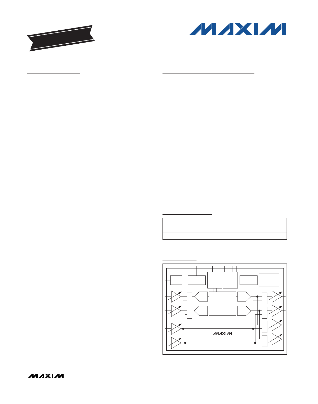
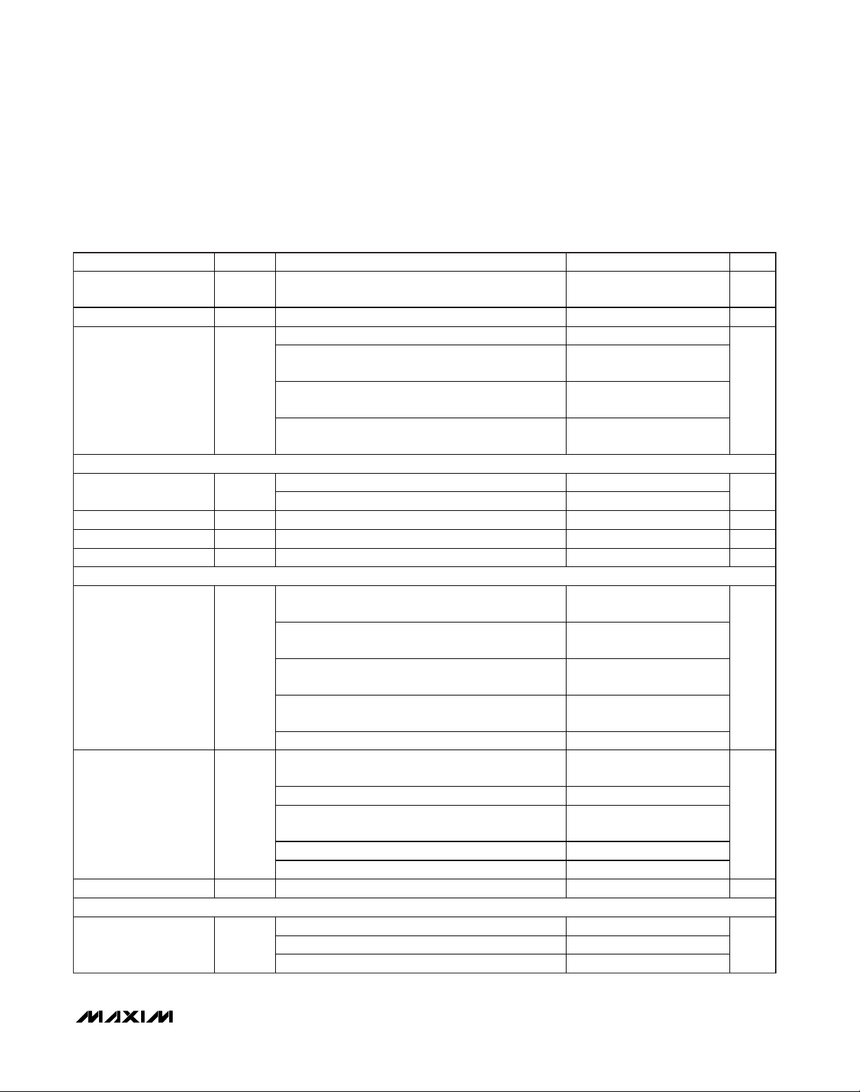
General Description
The MAX9880A is a high-performance, stereo audio
codec designed for portable consumer applications
such as smartphones and tablets. Operating from a single 1.8V supply to ensure low-power consumption, the
MAX9880A offers a variety of input and output configurations for design flexibility. The MAX9880A can be
combined with an audio subsystem, such as the
MAX9877 or MAX9879, for a complete audio solution
for portable applications.
The MAX9880A’s stereo differential microphone inputs
can support either analog or digital microphones. A
stereo single-ended line input, with a configurable preamplifier, can either be recorded by the ADC or routed
directly to the headphone or line output amplifiers. The
stereo headphone amplifiers can be configured as differential, single ended, or capacitorless. The stereo line
outputs have dedicated level adjustment.
There are two digital audio interfaces. The primary
interface is intended for voiceband applications, while
the secondary interface can be used for high performance stereo audio data. Two digital input streams can
be processed simultaneously and both digital interfaces support TDM and I2S data formats.
The flexible clocking circuitry utilizes any available
10MHz to 60MHz system clock, eliminating the need for
an external PLL and multiple crystal oscillators. Both
the ADC and DAC can be operated synchronously or
asynchronously in master or slave mode. The ADC can
be operated from 8kHz to 48kHz sample rates, while
the DAC can be operated up to 96kHz.
The MAX9880A prevents click and pop during volume
changes and during power-up and power-down. Audio
quality is further enhanced with user-configurable digital
filters for voice and audio data. Voiceband filters provide extra attenuation at the GSM packet frequency and
greater than 70dB stopband attenuation at fS/2. An I2C
or SPI™ serial interface provides control for volume levels, signal mixing, and general operating modes.
The MAX9880A is available in space-saving, 48-bump,
2.7mm x 3.5mm, 0.4mm-pitch WLP and 48-pin, 6mm x
6mm TQFN packages.
Applications
Cellular Phones
Tablet PCs
Portable Gaming Devices
Portable Multimedia Players
Features
o 1.8V Single-Supply Operation
o 10.6mW Playback Power Consumption
o 8kHz to 96kHz Stereo DAC with 96dB Dynamic
Range
o 8kHz to 48kHz Stereo ADC with 82dB Dynamic
Range
o Support for Any Master Clock Between 10MHz to
60MHz
o Stereo Microphone Inputs Support Digital
Microphones
o Stereo Headphone Amplifiers: Differential
(30mW), Single-Ended, or Capacitorless (10mW)
o Stereo Line Inputs and Stereo Line Outputs
o Voiceband Filters with Stopband Attenuation
Greater than 70dB
o Battery-Measurement Auxiliary ADC
o Comprehensive Headset Detection
o Dual I2S- and TDM-Compatible Digital Audio
Interfaces
o I2C- or SPI-Compatible Control Bus with 3.6V
Tolerant Inputs
MAX9880A
Low-Power, High-Performance
Dual I2S Stereo Audio Codec
________________________________________________________________
Maxim Integrated Products
1
Ordering Information
19-5139; Rev 1; 3/11
For pricing, delivery, and ordering information, please contact Maxim Direct at 1-888-629-4642,
or visit Maxim’s website at www.maxim-ic.com.
+
Denotes a lead(Pb)-free/RoHS-compliant package.
*
EP = Exposed pad.
EVALUATION KIT
AVAILABLE
PART TEMP RANGE PIN-PACKAGE
MAX9880AEWM+ -40°C to +85°C 48 WLP
MAX9880AETM+ -40°C to +85°C 48 TQFN-EP*
Functional Diagram/Typical Operating Circuit appears at
end of data sheet.
SPI is a trademark of Motorola, Inc.
MAX9880A
MIC
BIAS
MIX
LEFT
DIGITAL
FILTERING
RIGHT
LEFT
DAC
RIGHT
DAC
MIX
MIXMIXMIXMIX
DIGITAL
AUDIO
INTERFACE
1
MASTER
CLOCK
JACK SENSE/
MEASUREMENT
ADC
DIGITAL
AUDIO
INTERFACE
2
I2C
INTERFACE
Simplified Block Diagram
MAX9880A
Low-Power, High-Performance
Dual I
2
S Stereo Audio Codec
2 _______________________________________________________________________________________
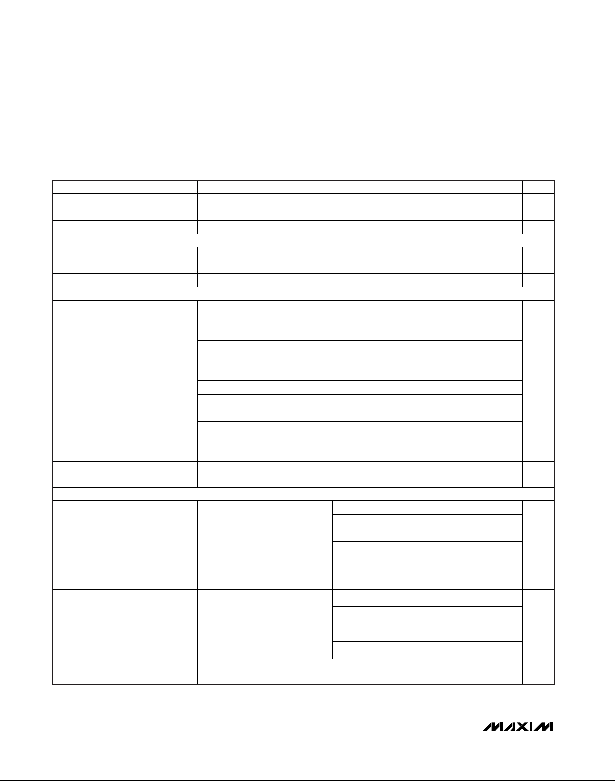
ABSOLUTE MAXIMUM RATINGS
ELECTRICAL CHARACTERISTICS
(V
AVDD
= V
PVDD
= V
MICVDD
= V
DVDD
= V
DVDDS1
= +1.8V, RL= ∞, headphone load (RL) connected between _OUTP and _OUTN, dif-
ferential modes, C
REF
= 2.2µF, C
MICBIAS
= C
PREG
= C
REG
= 1µF, AV
PRE
= +20dB, AV
PGAM
= 0dB, AV
DAC
= 0dB, AV
LINE
= +20dB,
AV
VOL
= 0dB, AVLO= 0dB, f
MCLK
= 13MHz, TA= T
MIN
to T
MAX
, unless otherwise noted. Typical values are at TA= +25°C.) (Note 2)
Stresses beyond those listed under “Absolute Maximum Ratings” may cause permanent damage to the device. These are stress ratings only, and functional
operation of the device at these or any other conditions beyond those indicated in the operational sections of the specifications is not implied. Exposure to
absolute maximum rating conditions for extended periods may affect device reliability.
(Voltages with respect to AGND.)
DVDD, AVDD, PVDD ................................................-0.3V to +2V
DVDDS1, JACKSNS, MICVDD ..............................-0.3V to +3.6V
DGND, PGND........................................................-0.1V to +0.1V
PREG, REF, REG ....................................-0.3V to (V
AVDD
+ 0.3V)
MICBIAS .............................................-0.3V to (V
MICVDD
+ 0.3V)
MCLK, LRCLKS1, BCLKS1,
SDINS1, SDOUTS1..........................-0.3V to (V
DVDDS1
+ 0.3V)
X1, X2, LRCLKS2, BCLKS2, SDINS2,
SDOUTS2, DOUT, MODE ...................-0.3V to (V
DVDD
+ 0.3V)
SDA/DIN, SCL/SCLK, CS, IRQ ..............................-0.3V to +3.6V
LOUTP, LOUTN, ROUTP, ROUTN,
LOUTL, LOUTR ....................(V
PGND
- 0.3V) to (V
PVDD
+ 0.3V)
LINL, LINR, MICLP/DIGMICDATA,
MICLN/DIGMICCLK, MICRP/SPDMDATA,
MICRN/SPDMCLK ...............................-0.3V to (V
AVDD
+ 0.3V)
Continuous Power Dissipation (T
A
= +70°C)
48-Bump WLP (derate 12.5mW/°C above +70°C) .....1000mW
48-Pin TQFN (derate 37mW/°C above +70°C) ..........2963mW
Junction Temperature......................................................+150°C
Operating Temperature Range ...........................-40°C to +85°C
Storage Temperature Range .............................-65°C to +150°C
Lead Temperature (soldering, 10s) .................................+300°C
Soldering Temperature (reflow) .......................................+260°C
Note 1: Package thermal resistances were obtained using the method described in JEDEC specification JESD51-7, using a four-
layer board. For detailed information on package thermal considerations, refer to www.maxim-ic.com/thermal-tutorial
.
PACKAGE THERMAL CHARACTERISTICS (Note 1)
TQFN
Junction-to-Ambient Thermal Resistance (θ
JA
)...............27°C/W
Junction-to-Case Thermal Resistance (θ
JC
)......................1°C/W
WLP
Junction-to-Ambient Thermal Resistance (θ
JA
)................42°C/W
Junction-to-Case Thermal Resistance (θ
JC
).......................5°C/W
PARAMETER SYMBOL CONDITIONS MIN TYP MAX UNITS
Supply Voltage Range
Total Supply Current I
Shutdown Supply
Current
Shutdown to Full
Operation
VDD
T
Excludes PLL lock time 10 ms
PVDD, DVDD, AVDD 1.65 1.8 1.95
DVDDS1, MICVDD 1.65 1.8 3.6
Ful l-duple x 8 kHz
mono (Note 3)
DAC playback
48kHz stereo
(Note 3)
Full-duplex 48kHz
stereo (Note 3)
Stereo line-in to
line-out only,
= +25°C
T
A
= +25°C
A
Analog (AVDD + PVDD +
MICVDD)
Digital (DVDD + DVDDS1) 1.4 2
Analog (AVDD + PVDD +
MICVDD)
Digital (DVDD + DVDDS1) 2.5 4
Analog (AVDD + PVDD +
MICVDD)
Digital (DVDD + DVDDS1) 3.0 5
Analog (AVDD + PVDD +
MICVDD)
Digital (DVDD + DVDDS1) 0.012 0.05
Analog (AVDD + PVDD +
MICVDD)
Digital (DVDD + DVDDS1) 2.6 8
5.33 8
3.5 6
8.4 12
4.9 8
0.3 2
V
mA
µA
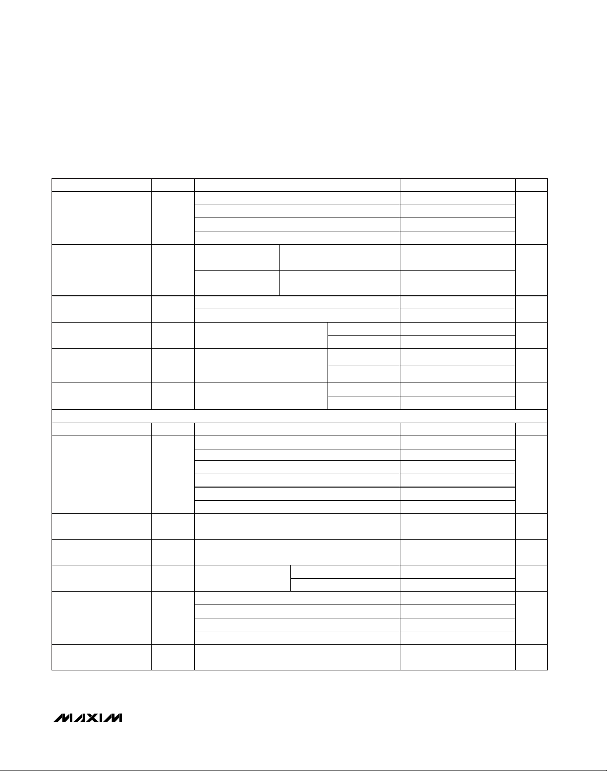
MAX9880A
Low-Power, High-Performance
Dual I2S Stereo Audio Codec
_______________________________________________________________________________________ 3
ELECTRICAL CHARACTERISTICS (continued)
(V
AVDD
= V
PVDD
= V
MICVDD
= V
DVDD
= V
DVDDS1
= +1.8V, RL= ∞, headphone load (RL) connected between _OUTP and _OUTN, dif-
ferential modes, C
REF
= 2.2µF, C
MICBIAS
= C
PREG
= C
REG
= 1µF, AV
PRE
= +20dB, AV
PGAM
= 0dB, AV
DAC
= 0dB, AV
LINE
= +20dB,
AV
VOL
= 0dB, AVLO= 0dB, f
MCLK
= 13MHz, TA= T
MIN
to T
MAX
, unless otherwise noted. Typical values are at TA= +25°C.) (Note 2)
PARAMETER SYMBOL CONDITIONS MIN TYP MAX UNITS
DAC (Note 4)
Dynamic Range
(Note 5)
Ful l-Scale Output
Gain Error
Voice Path Phase Delay P
Total Harmonic
Distortion
DAC Attenuation Range AV
DAC Gain Adju st AV
Power-Supply Rejection
Ratio
DAC VOICE MODE DIGITAL IIR LOWPASS FILTER (6x Interpolation)
Passband Cutoff f
Passband Ripple f < f
Stopband Cutoff f
Stopband Attenuation f > f
DAC VOICE MODE DIGITAL 5th-ORDER IIR HIGHPASS FILTER
5th-Order Passband
Cutoff
(-3dB from Peak,
2
I
C Register
Programmable)
fS = 48kHz, AV
DR
T
= +25°C
A
= 0dB,
VOL
Master or slave mode 96
Slave mode 88
Differential mode 1
Capacitorle ss and single-ended modes 0.56
DC accuracy, mea sured with respect to full-sca le
output
1kHz, 0dB input, highpass
filter disabled measured from
DLY
digital input to analog output;
MODE = 0 (IIR voice)
f
= 12.288MHz, fS = 48kHz, 0dBFS, measured
THD
GAIN
PSRR
PLP
SLP
MCLK
at headphone outputs
VDACA/SDACA = 0xF to 0 x0 -15 0 dB
DAC
VDACG = 00 to 11 0 +18 dB
V
= V
AVDD
f = 217Hz, V
f = 1 kH z, V
f = 10kHz, V
= 1.65V to 1.95V 85
PVDD
= 100mV
RIPPLE
= 100mV
RIPPLE
= 100mV
RIPPLE
With respect to fS within ripple; fS = 8kHz to 48kHz 0.448 x f
-3dB cutoff 0.451 x f
PLP
With respect to fS; fS = 8kHz to 48 kHz 0.476 x f
, f = 20Hz to 20kHz 75 dB
SLP
fS = 8kHz 1.2
= 16kHz 0.59
f
S
P-P
P-P
P-P
, AV
, AV
, AV
= 0dB 85
VOL
= 0dB 80
VOL
= 0dB 74
VOL
DVFLT = 0x1
(Elliptical tuned for 16kHz GSM + 217Hz notch)
DVFLT = 0x2
(500Hz Butterworth tuned for 16kHz)
f
DHPPB
DVFLT = 0x3
(Elliptical tuned for 8kHz GSM + 217Hz notch)
DVFLT = 0x4
(500Hz Butterworth tuned for 8kHz)
DVFLT = 0x5
(f
/240 Butterworth)
S
1 5 %
-75 dB
±0.1 dB
0.0161 x
f
S
0.0312 x
f
S
0.0321 x
f
S
0.0625 x
f
S
0.0042 x
f
S
S
S
S
dB
V
RMS
ms
dB
Hz
Hz
Hz
MAX9880A
Low-Power, High-Performance
Dual I2S Stereo Audio Codec
4 _______________________________________________________________________________________
(
)
ELECTRICAL CHARACTERISTICS (continued)
(V
AVDD
= V
PVDD
= V
MICVDD
= V
DVDD
= V
DVDDS1
= +1.8V, RL= ∞, headphone load (RL) connected between _OUTP and _OUTN, dif-
ferential modes, C
REF
= 2.2µF, C
MICBIAS
= C
PREG
= C
REG
= 1µF, AV
PRE
= +20dB, AV
PGAM
= 0dB, AV
DAC
= 0dB, AV
LINE
= +20dB,
AV
VOL
= 0dB, AVLO= 0dB, f
MCLK
= 13MHz, TA= T
MIN
to T
MAX
, unless otherwise noted. Typical values are at TA= +25°C.) (Note 2)
PARAMETER SYMBOL CONDITIONS MIN TYP MAX UNITS
5th-Order Stopband
Cutoff
(-30dB from Peak,
2
I
C Register
Programmable)
DC Attenuation DC
DAC STEREO AUDIO MODE DIGITAL FIR LOWPASS FILTER (DHF = 0 for f
Passband Cutoff f
Passband Ripple f < f
Stopband Cutoff f
Stopband Attenuation f > f
DAC STEREO AUDIO MODE DIGITAL FIR LOWPASS FILTER (DHF = 1 for f
Passband Cutoff f
Passband Ripple f < f
Stopband Cutoff f
Stopband Attenuation f > f
DAC STEREO AUDIO MODE DIGITAL DC-BLOCKING HIGHPASS FILTER
Passband Cutoff
(-3dB from Peak)
DC Attenuation DC
ADC (Note 6)
Dynamic Range
(Note 5)
Ful l-Scale Input
Gain Error (Note 7)
Voice Path Phase Delay
DVFLT = 0x1
(Elliptical tuned for 16kHz GSM + 217Hz notch)
DVFLT = 0x2
(500Hz Butterworth tuned for 16kHz)
f
DHPSB
DVFLT = 0x3
(Elliptical tuned for 8kHz GSM + 217Hz notch)
DVFLT = 0x4
(500Hz Butterworth tuned for 8kHz)
DVFLT = 0x5
/240 Butterworth)
(f
S
DVFLT not equal to 000 90 dB
ATTEN
With respect to fS within ripple; fS = 8kHz to 48kHz 0.43 x f
PLP
-3dB cutoff 0.47 x f
-6.02dB cutoff 0.50 x f
PLP
SLP
PLP
SLP
f
DHPPB
ATTEN
DR
With respect to f
to 7.42 f
S
60 dB
SLP
Ripple limit cutoff 0.24 x f
-3dB cutoff 0.33 x f
±0.1 dB
PLP
With respect to fS; f = 0.5 fS to 3.5 fS 0.5 x fS Hz
60 dB
SLP
DVFLT = 0x1 (DAI1), DCB = 1 (DAI2)
DVFLT = 0x1 (DAI1), DCB = 1 (DAI2) 90 dB
fS = 8kHz, MODE = 0 (IIR voice), TA = +25°C 72 82
f
= 8kHz to 48kHz, MODE = 1 (FIR audio) (Note 7) 84
S
; fS = 8kHz to 48kHz; f = 0.58 f
S
Differential MIC input or stereo line inputs,
AV
= 0dB, AV
PRE
PGAM
= 0dB
DC accuracy, measured with respect to 80% of fu llscale output
1kH z, 0dB input, highpass
filter disabled measured from
analog input to digital output;
MODE = 0
IIR voice
fS = 8kHz 1.2
f
S
0.0139 x
f
S
0.0156 x
f
S
0.0279 x
f
S
0.0312 x
f
S
0.0021 x
f
S
< 50kHz)
LRCLK
S
S
S
±0.1 dB
LRCLK
S
> 50kHz)
0.58 x f
S
S
S
0.000625 x
f
S
1 V
1 5 %
= 16kHz 0.61
Hz
Hz
Hz
Hz
Hz
dB
P-P
ms
MAX9880A
Low-Power, High-Performance
Dual I2S Stereo Audio Codec
_______________________________________________________________________________________ 5
ELECTRICAL CHARACTERISTICS (continued)
(V
AVDD
= V
PVDD
= V
MICVDD
= V
DVDD
= V
DVDDS1
= +1.8V, RL= ∞, headphone load (RL) connected between _OUTP and _OUTN, dif-
ferential modes, C
REF
= 2.2µF, C
MICBIAS
= C
PREG
= C
REG
= 1µF, AV
PRE
= +20dB, AV
PGAM
= 0dB, AV
DAC
= 0dB, AV
LINE
= +20dB,
AV
VOL
= 0dB, AVLO= 0dB, f
MCLK
= 13MHz, TA= T
MIN
to T
MAX
, unless otherwise noted. Typical values are at TA= +25°C.) (Note 2)
PARAMETER SYMBOL CONDITIONS MIN TYP MAX UNITS
Total Harmonic
Distortion
ADC Level Adjust
Power-Supply Rejection
Ratio
ADC VOICE MODE DIGITAL IIR LOWPASS FILTER
Passband Cutoff f
Passband Ripple f < f
Stopband Cutoff f
Stopband Attenuation f > f
ADC VOICE MODE DIGITAL 5th-ORDER IIR HIGHPASS FILTER
Passband Cutoff
(-3dB from Peak)
Stopband Cutoff
(-30dB from Peak)
DC Attenuation DC
ADC STEREO AUDIO MODE DIGITAL FIR LOWPASS FILTER
Passband Cutoff f
THD f = 1kH z, f
AV
PSRR
f
AHPPB
f
AHPSB
AVL/AVR = 0xF to 0x0 -12 +3 dB
ADC
V
AVDD
f = 217Hz, V
input referred
f = 1 kH z, V
referred
f = 10kHz, V
input referred
PLP
SLP
With respect to fS within ripple; fS = 8kHz to 48kHz 0.445 x f
-3dB cutoff 0.449 x f
With respect to fS; fS = 8kHz to 48 kHz 0.469 x fS Hz
AVFLT = 0x1
(Elliptical tuned for 16kHz GSM + 217Hz notch)
AVFLT = 0x2
(500Hz Butterworth tuned for 16kHz)
AVFLT = 0x3
(Elliptical tuned for 8kHz GSM + 217Hz notch)
AVFLT = 0x4
(500Hz Butterworth tuned for 8kHz)
AVFLT = 0x5 (fS/240 Butterworth) 0.0042 x f
AVFLT = 0x1 (Elliptical tuned for 16kHz GSM +
217Hz notch)
AVFLT = 0x2 (500Hz Butterworth tuned for 16kHz) 0.0156 x f
AVFLT = 0x3 (Elliptical tuned for 8kHz GSM +
217Hz notch)
AVFLT = 0x4 (500Hz Butterworth tuned for 8kHz) 0.0312 x f
AVFLT = 0x5 (fS/240 Butterworth) 0.0021 x f
AVFLT 000 90 dB
ATTEN
With respect to fS within ripple; fS = 8kHz to 48kHz 0.43 x f
PLP
-3dB cutoff 0.48 x f
-6.02dB cutoff 0.5 x f
= 8kHz, TA = +25°C, -20dB input -80 -70 dB
S
= 1.65V to 1.95V, input referred 60 80
= 100mV
RIPPLE
= 100mV
RIPPLE
= 100mV
RIPPLE
±0.1 dB
PLP
, f = 20Hz to 20kHz 74 dB
SLP
P-P
P-P
P-P
, AV
, AV
, AV
= 0dB,
ADC
= 0dB, input
ADC
= 0dB,
ADC
80
78
72
S
S
0.0161 x
f
S
0.0312 x
f
S
0.0321 x
f
S
0.0625 x
f
S
S
0.0139 x
f
S
S
0.0279 x
f
S
S
S
S
S
S
dB
Hz
Hz
Hz
Hz
MAX9880A
Low-Power, High-Performance
Dual I2S Stereo Audio Codec
6 _______________________________________________________________________________________
ELECTRICAL CHARACTERISTICS (continued)
(V
AVDD
= V
PVDD
= V
MICVDD
= V
DVDD
= V
DVDDS1
= +1.8V, RL= ∞, headphone load (RL) connected between _OUTP and _OUTN, dif-
ferential modes, C
REF
= 2.2µF, C
MICBIAS
= C
PREG
= C
REG
= 1µF, AV
PRE
= +20dB, AV
PGAM
= 0dB, AV
DAC
= 0dB, AV
LINE
= +20dB,
AV
VOL
= 0dB, AVLO= 0dB, f
MCLK
= 13MHz, TA= T
MIN
to T
MAX
, unless otherwise noted. Typical values are at TA= +25°C.) (Note 2)
PARAMETER SYMBOL CONDITIONS MIN TYP MAX UNITS
Passband Ripple f < f
Stopband Cutoff f
Stopband Attenuation f > f
ADC STEREO AUDIO MODE DIGITAL DC-BLOCKING HIGHPASS FILTER
Passband Cutoff
(-3dB from Peak)
DC Attenuation DC
OUTPUT VOLUME CONTROL
Output Vo lu me Control
(Note 8)
Output Vo lu me Control
Step Size
Output Vo lu me Control
Mute Attenuation
HEADPHONE AMPLIFIER (Note 9)
Output Power
(Differential Mode)
Output Power
(Capacitorless Mode)
Total Harmonic
Distortion + Noise
(Differential Mode)
Total Harmonic
Distortion + Noise
(Capacitorless Mode)
Total Harmonic
Distortion + Noise
(Single-Ended Mode)
Dynamic Range
(Notes 5, 7)
f
AHPPB
P
P
THD+N f = 1kHz, -3dBFS input
THD+N f = 1kHz, -3dBFS input
THD+N f = 1kHz, -3dBFS input
With respect to fS; fS = 8kHz to 48 kHz 0.58 x fS Hz
SLP
AVFLT = 0x1
AVFLT = 0x1 90 dB
ATTEN
VOLL/VOLR = 0x00 8.1 8.6 9.2
VOLL/VOLR = 0x01 7.6 8.1 8.6
VOLL/VOLR = 0x02 7.1 7.6 8.1
VOLL/VOLR = 0x04 6.1 6.6 7.2
VOLL/VOLR = 0x08 3.1 3.6 4.3
VOLL/VOLR = 0x10 -5.9 -5.4 -4.9
VOLL/VOLR = 0x20 -60 -55.1 -52
VOLL/VOLR = 0x27 -94 -84 -81
VOLL/VOLR = 00 x00 to 0x06 (+9dB to +6dB) 0.5
VOLL/VOLR = 00 x06 to 0x0F (+6dB to +3dB) 1
VOLL/VOLR = 00 x0F to 0x17 (-3dB to -19dB) 2
VOLL/VOLR = 00 x17 to 0x27 (-19dB to -81dB) 4
f = 1kHz 100 dB
f = 1kHz, 0dBFS input,
OUT
THD < 1%, T
f = 1kHz, 0dBFS input,
OUT
THD < 1%, T
DR AV
PLP
, f = 20Hz to 20kHz 60 dB
SLP
= +6dB 77 90 dB
VOL
= +25°C
A
= +25°C
A
RL = 16 25 48
R
= 32 30
L
RL = 16 17
R
= 32 10
L
RL = 16 -78 -67
R
= 32 -79
L
RL = 16 -73 -60
R
= 32 -75
L
RL = 16 -70 -60
R
= 32 -70
L
±0.1 dB
0.000625
x f
S
Hz
dB
dB
mW
mW
dB
dB
dB
MAX9880A
Low-Power, High-Performance
Dual I2S Stereo Audio Codec
_______________________________________________________________________________________ 7
ELECTRICAL CHARACTERISTICS (continued)
(V
AVDD
= V
PVDD
= V
MICVDD
= V
DVDD
= V
DVDDS1
= +1.8V, RL= ∞, headphone load (RL) connected between _OUTP and _OUTN, dif-
ferential modes, C
REF
= 2.2µF, C
MICBIAS
= C
PREG
= C
REG
= 1µF, AV
PRE
= +20dB, AV
PGAM
= 0dB, AV
DAC
= 0dB, AV
LINE
= +20dB,
AV
VOL
= 0dB, AVLO= 0dB, f
MCLK
= 13MHz, TA= T
MIN
to T
MAX
, unless otherwise noted. Typical values are at TA= +25°C.) (Note 2)
PARAMETER SYMBOL CONDITIONS MIN TYP MAX UNITS
Power-Supply Rejection
Ratio (Note 7)
Output Offset Voltage V
Crosstalk XTALK
Capaciti ve Drive
Capability
Click-and-Pop Leve l
(Differential,
Capacitorless Modes)
Click-and-Pop Leve l
(Single-Ended Mode)
LINE OUTPUTS (Note 7)
Ful l-Scale Output 0.5 V
Line Output Level
Adjust
Line Output Mute
Attenuat ion
Total Harmonic
Distortion + Noise
Signal-to-Noise Ratio
Power-Supply Rejection
Ratio
Capaciti ve Drive
Capability
PSRR
V
AVDD
f = 217Hz, V
f = 1 kH z, V
f = 10kHz, V
AV
different ia l mode
OS
AV
capacitorless mode
Differential, P
Capacitorless mode, P
= V
= -81dB,
VOL
PVDD
RIPPLE
= 1.65V to 1.95V 60 80
= 100mV
RIPPLE
RIPPLE
= 100mV
= 100mV
P-P
P-P
P-P
LOUTP to LOUTN, ROUTP to
ROUTN, T
= -81dB,
VOL
LOUTP to LOUTN, ROUTP to
LOUTN, T
= 5mW, f = 1kHz 90
OUT
= 5mW, f = 1kHz 45
OUT
No sustained oscillations
Peak voltage, A-weighted,
32 samples per second
Peak voltage, A-weighted,
32 samples per second
, AV
VOL
, AV
VOL
, AV
VOL
= +25°C
A
= +25°C
A
= 0dB 80
= 0dB 78
= 0dB 72
±0.2
±0.6
RL = 32 500
R
= 100
L
Into shutdown -70
Out of shutdown -70
Into shutdown -70
Out of shutdown -70
LOGL/LOGR = 0x00 -0.7 -0.1 +0.6
LOGL/LOGR = 0x01 -2.6 -2.1 -1.6
AV
LOGL/LOGR = 0x02 -4.6 -4.1 -3.6
LO
LOGL/LOGR = 0x04 -8.6 -8.1 -7.6
LOGL/LOGR = 0x08 -16.6 -16 -15.6
LOGL/LOGR = 0x0F -31.1 -29.9 -29.1
f = 1kHz 90 dB
THD+N R
PSRR
R
= 1k, f = 1kHz, V
L
R
= 1k, LINL/LINR =
L
1µF to GND
V
= V
AVDD
f = 217Hz, V
f = 1 kH z, V
f = 10kHz, V
= 10k, no sustained oscillations 100 pF
L
= 1.65V to 1.95V 46
PVDD
RIPPLE
= 100mV
RIPPLE
RIPPLE
OUT
= 1.4V
(Note 9) -67 -59 dB
P-P
20Hz < f < 20 kHz 86
A-weighted 90
= 100mV
= 100mV
P-P
P-P
P-P
, AV
, AV
, AV
= 0dB 78
VOL
= 0dB 80
VOL
= 0dB 76
VOL
dB
mV
dB
pF
dBV
dBV
RMS
dB
dB
dB
MAX9880A
Low-Power, High-Performance
Dual I2S Stereo Audio Codec
8 _______________________________________________________________________________________
ELECTRICAL CHARACTERISTICS (continued)
(V
AVDD
= V
PVDD
= V
MICVDD
= V
DVDD
= V
DVDDS1
= +1.8V, RL= ∞, headphone load (RL) connected between _OUTP and _OUTN, dif-
ferential modes, C
REF
= 2.2µF, C
MICBIAS
= C
PREG
= C
REG
= 1µF, AV
PRE
= +20dB, AV
PGAM
= 0dB, AV
DAC
= 0dB, AV
LINE
= +20dB,
AV
VOL
= 0dB, AVLO= 0dB, f
MCLK
= 13MHz, TA= T
MIN
to T
MAX
, unless otherwise noted. Typical values are at TA= +25°C.) (Note 2)
PARAMETER SYMBOL CONDITIONS MIN TYP MAX UNITS
MICROPHONE AMPLIFIER
Preamplifier Gain AV
MIC PGA Gain AV
Common-Mode
Reject ion Ratio
MIC Input Resistance RIN_MIC All gain settings 30 50 k
Total Harmonic
Distortion + Noise
Power-Supply Rejection
Ratio
MICROPHONE BIAS
MICBIAS Output Voltage V
Load Regulation I
Line Regulation V
Power-Supply Rejection
Ratio
Noise Voltage A-weighted 9.5 µV
LINE INPUT
Ful l-Scale Input VIN AV
Line Input Level Adjust AV
PALEN/PAREN = 01 -0.5 0 +0.5
PALEN/PAREN = 10 19.5 20 20.5
PRE
PALEN/PAREN = 11 29.3 30 30.5
PGAM
CMRR V
PGAML/PGAMR = 0x1F -0.5 0 +0.6
PGAML/PGAMR = 0x00 19.3 19.9 20.4
IN
AV
V
THD+N
IN
AV
V
IN
V
AVDD
f = 217Hz, V
referred
PSRR
f = 1 kH z, V
referred
f = 10kHz, V
referred
MICBIAS ILOAD
LOAD
AVDD
PSRR
f = 217Hz, V
f = 10kHz, V
LIGL/LIGR = 0x00 22.8 23.9 24.9
LIGL/LIGR = 0x01 20.7 21.9 22.9
LIGL/LIGR = 0x02 18.9 20 20.9
LINE
LIGL/LIGR = 0x04 14.9 16 16.9
LIGL/LIGR = 0x08 6.9 8 8.9
= 100mV
= 0dB
PRE
= 1V
P-P
= +30dB
PRE
= 32mV
, f = 1kHz, A-weighted
P-P
, f = 217Hz 50 dB
P-P
-80
, f = 1kHz, A-weighted
-65
= 1.65V to 1.95V, input referred 60 80
RIPPLE
= 1mA
= 100mV, AV
RIPPLE
= 100mV, AV
= 100mV, AV
RIPPLE
V
MICVDD
V
MICVDD
= 1.8V, MBIAS = 0 1.48 1.52 1.56
= 3V, MBIAS = 0 2.15 2.2 2.25
= 0dB, input
ADC
= 0dB, input
ADC
= 0dB, input
ADC
80
78
72
= 1mA to 2mA, MBIAS = 0 0.6 10 V/A
= 1.8V, V
RIPPLE
RIPPLE
= 0dB 1.0 V
LINE
= 1.65V to 1.95V, MBIAS = 0 1.55 mV/V
MICVDD
= 100mV
= 100mV
100
P-P
90
P-P
dB
dB
dB
dB
V
dB
RMS
P-P
dB
MAX9880A
Low-Power, High-Performance
Dual I
2
S Stereo Audio Codec
_______________________________________________________________________________________ 9
ELECTRICAL CHARACTERISTICS (continued)
(V
AVDD
= V
PVDD
= V
MICVDD
= V
DVDD
= V
DVDDS1
= +1.8V, RL= ∞, headphone load (RL) connected between _OUTP and _OUTN, dif-
ferential modes, C
REF
= 2.2µF, C
MICBIAS
= C
PREG
= C
REG
= 1µF, AV
PRE
= +20dB, AV
PGAM
= 0dB, AV
DAC
= 0dB, AV
LINE
= +20dB,
AV
VOL
= 0dB, AVLO= 0dB, f
MCLK
= 13MHz, TA= T
MIN
to T
MAX
, unless otherwise noted. Typical values are at TA= +25°C.) (Note 2)
PARAMETER SYMBOL CONDITIONS MIN TYP MAX UNITS
Line Input Mute
Attenuat ion
Input Resistance R
Total Harmonic
Distortion + Noise
AUXIN INPUT
Input DC Voltage Range AUXEN = 1 0 0.738 V
AUXIN Input Resistance R
JACK DETECT
JACKSNS High
Threshold
JACKSNS Low
Threshold
JACKSNS Sense
Voltage
JACKSNS Sense
Resistance
JACKSNS Deglitch
Period
Headphone Sense
Threshold
1-BIT SPDM OUTPUT
Dynamic Range
(Note 5)
Output Operational
Range
DIGITAL SIDETONE (MODE = 1 IIR Voice Mode Only)
Sidetone Gain Adjust
Range
Voice Path Phase Delay P
IN_LINE
THD+N V
V
V
V
SENSE
R
SENSE
t
GLITCH
AV
f = 1kHz 100 dB
AV
IN
AUXEN = 1, 0V V
IN
SHDN = 1
TH1
SHDN = 0
SHDN = 1
TH2
SHDN = 0
SHDN = 0 V
SHDN = 0 1.9 2.3 3.1 k
12 300 ms
f
= 48kHz, A-weighted, 20Hz to 20kHz,
DR
STGA
DLY
S
AV
0dB signa l 1’s density 25 75 %
Differential output mode -60 0 dB
MIC input to headphone
output, f = 1 kH z, HP filter
disabled
= +24dB 20 k
LINE
= 0.1V
P-P
= 0dB; ma ster or sla ve mode, TA = +25°C
VOL
, f = 1kHz -74 dB
0.738V
AUXIN
fS = 8kHz 2.2
= 16kHz 1.1
f
S
10 40 M
0.92 x
V
MICBIAS
0.06 x
V
MICBIAS
90 dB
0.95 x
V
MICBIAS
0.95 x
V
MICVDD
0.10 x
V
MICBIAS
0.08 x
V
MICVDD
MICVDD
V
V
V
8
0.98 x
MICBIAS
0.17 x
MICBIAS
V
V
ms
MAX9880A
Low-Power, High-Performance
Dual I2S Stereo Audio Codec
10 ______________________________________________________________________________________
ELECTRICAL CHARACTERISTICS (continued)
(V
AVDD
= V
PVDD
= V
MICVDD
= V
DVDD
= V
DVDDS1
= +1.8V, RL= ∞, headphone load (RL) connected between _OUTP and _OUTN, dif-
ferential modes, C
REF
= 2.2µF, C
MICBIAS
= C
PREG
= C
REG
= 1µF, AV
PRE
= +20dB, AV
PGAM
= 0dB, AV
DAC
= 0dB, AV
LINE
= +20dB,
AV
VOL
= 0dB, AVLO= 0dB, f
MCLK
= 13MHz, TA= T
MIN
to T
MAX
, unless otherwise noted. Typical values are at TA= +25°C.) (Note 2)
PARAMETER SYMBOL CONDITIONS MIN TYP MAX UNITS
INPUT CLOCK CHARACTERISTICS
MCLK Input Frequency f
MCLK Input Duty Cycle
Maximum MCLK Input
Jitter
LRCLK Sample Rate
(Note 10)
LRCLK Average
Frequency Error (Master
and Slave Modes)
(Note 11)
LRCLK PLL Lock Time
LRCLK Acceptable
Jitter for Maintaining
PLL Lock
Soft-Start/Stop Time 10 ms
CRYSTAL OSCILLATOR
Frequency Fundamental mode only 12.288 MHz
Maximum Crystal ESR 100
Input Leakage Current IIH, IIL X1, TA = +25°C -1 +1 µA
Input Capacitance CX1, CX2 4 pF
Maximum Load
Capacitor
DIGITAL INPUT (MCLK)
Input High Voltage VIH 1.2 V
Input Low Voltage VIL 0.6 V
Input Leakage Current IIH, IIL TA = +25°C -1 +1 µA
Input Capacitance 10 pF
DIGITAL INPUTS (SDINS1, BCLKS1, LRCLKS1)
Input High Voltage V
Input Low Voltage VIL
Input Hysteresis 200 mV
Input Leakage Current IIH, IIL TA = +25°C -1 +1 µA
Input Capacitance 10 pF
MCLK
C
L1
Maxi mum a llowable RMS for performance limit s 100 ps
, CL2 45 pF
IH
For any LRCLK sample rate 10 60 MHz
Prescaler = /1 mode 40 60
/2 or /4 modes 30 70
DHF = 0 8 48
DHF = 1 48 96
FREQ1 mode = 0x8 to 0xF 0 0
PCLK = 192x, 256x, 384x, 512x, 768x, and 1024x 0 0
FREQ1 mode = An y c lock other than above -0.025 +0.025
Any al lowable LRCLK and
PCLK rate, slave mode
Allowable LRCLK period change from nominal for
slave PLL mode at any allowable LRCLK and PCLK
rates
Rapid lock mode 2 7
Nonrapid lock mode 12 25
0.7
x V
DVDDS1
V
±100 ns
0.3
x V
DVDDS1
%
kHz
%
ms
V
MAX9880A
Low-Power, High-Performance
Dual I2S Stereo Audio Codec
______________________________________________________________________________________ 11
ELECTRICAL CHARACTERISTICS (continued)
(V
AVDD
= V
PVDD
= V
MICVDD
= V
DVDD
= V
DVDDS1
= +1.8V, RL= ∞, headphone load (RL) connected between _OUTP and _OUTN, dif-
ferential modes, C
REF
= 2.2µF, C
MICBIAS
= C
PREG
= C
REG
= 1µF, AV
PRE
= +20dB, AV
PGAM
= 0dB, AV
DAC
= 0dB, AV
LINE
= +20dB,
AV
VOL
= 0dB, AVLO= 0dB, f
MCLK
= 13MHz, TA= T
MIN
to T
MAX
, unless otherwise noted. Typical values are at TA= +25°C.) (Note 2)
PARAMETER SYMBOL CONDITIONS MIN TYP MAX UNITS
DIGITAL INPUTS (SDA, SCL, DIN, SCLK, CS, MODE, SDINS2, BCLKS2, LRCLKS2)
Input High Voltage V
Input Low Voltage VIL
Input Hysteresis 200 mV
Input Leakage Current IIH, IIL TA = +25°C -1 +1 µA
Input Capacitance 10 pF
DIGITAL INPUTS (DIGMICDATA)
Input High Voltage V
Input Low Voltage VIL
Input Hysteresis 100 mV
Input Leakage Current IIH, IIL TA = +25°C -35 +35 µA
Input Capacitance 10 pF
CMOS DIGITAL OUTPUTS (BCLKS1, LRCLKS1, SDOUTS1)
Output Low Voltage VOL IOL = 3mA 0.4 V
Output High Voltage VOH IOH = 3mA
CMOS DIGITAL OUTPUTS (BCLKS2, LRCLKS2, SDOUTS2)
Output Low Voltage VOL IOL = 3mA 0.4 V
Output High Voltage VOH IOH = 3mA
CMOS DIGITAL OUTPUTS (DOUT)
Output Low Voltage VOL IOL = 1mA, CS = DVDD 0.4 V
Output High Voltage VOH IOH = 1mA, CS = DVDD
Output Low Current IOL MODE = DVDD, DOUT = 0, TA = +25°C -1 +1 µA
Output High Current IOH MODE = DVDD, DOUT = DVDD, TA = +25°C -1 +1 µA
CMOS DIGITAL OUTPUTS (DIGMICCLK, SPDMDATA, SPDMCLK)
Output Low Voltage VOL IOL = 1mA 0.4 V
Output High Voltage VOH IOH = 1mA
OPEN-DRAIN DIGITAL OUTPUTS (SDA, IRQ)
Output High Current IOH V
Output Low Voltage VOL IOL = 3mA
IH
IH
= V
OUT
DVDD
, TA = +25°C -1 +1 µA
0.7
x V
DVDD
0.65
x V
DVDD
V
DVDDS1
- 0.4
V
DVDD
- 0.4
V
DVDD
- 0.4
V
DVDD
- 0.4
V
V
V
V
V
V
x V
x V
x V
0.3
DVDD
0.35
DVDD
0.2
DVDD
V
V
V
MAX9880A
Low-Power, High-Performance
Dual I2S Stereo Audio Codec
12 ______________________________________________________________________________________
ELECTRICAL CHARACTERISTICS (continued)
(V
AVDD
= V
PVDD
= V
MICVDD
= V
DVDD
= V
DVDDS1
= +1.8V, RL= ∞, headphone load (RL) connected between _OUTP and _OUTN, dif-
ferential modes, C
REF
= 2.2µF, C
MICBIAS
= C
PREG
= C
REG
= 1µF, AV
PRE
= +20dB, AV
PGAM
= 0dB, AV
DAC
= 0dB, AV
LINE
= +20dB,
AV
VOL
= 0dB, AVLO= 0dB, f
MCLK
= 13MHz, TA= T
MIN
to T
MAX
, unless otherwise noted. Typical values are at TA= +25°C.) (Note 2)
PARAMETER SYMBOL CONDITIONS MIN TYP MAX UNITS
DIGITAL MICROPHONE TIMING CHARACTERISTICS (V
DIGMICCLK Frequency f
DIGMICDATA to
DIGMICCLK Setup Time
DIGMICDATA to
DIGMICCLK Hold Time
SPDM TIMING CHARACTERISTICS
SPDMCLK Frequency f
SPDMCL K to
SPDMDATA Dela y T ime
DIGITAL AUDIO INTERFACE TIMING CHARACTERISTICS (TDM = 0, V
BCLK Cycle Time t
BCLK High Time t
BCLK Low Time t
BCLK or LRCLK Rise
and Fall Time
SDIN or LRCLK to BCLK
Setup Time
SDIN or LRCLK to BCLK
Hold Time
SDOUT Delay Time from
BCLK Ris ing Edge
DIGITAL AUDIO INTERFACE TIMING CHARACTERISTICS (TDM = 1, Figure 3, V
TDM Cloc k Frequency 1/t
TDM Clock Time High t
TDM Clock Time Low t
TDM Short-Sync Setup
Time
= 1.8V)
DVDD
MICCLK = 00 1.536
MICCLK
f
= 12.288MHz
MCLK
MICCLK = 01 2.048
MICCLK = 10 64f
t
Either clock edge 20 ns
SU, M IC
Either clock edge 0 ns
t
HD, M I C
SPDMCLK = 00 1.536
SPDMCLK fMCLK
= 12.288MHz
SPDMCLK = 01 2.048
SPDMCLK = 10 3.072
Risi ng edge SPDMCLK
Minimum, f
Maximum, f
t
DLY, SP DM
to right-channel valid
SPDMDATA and falling
edge SPDMCLK to leftchannel valid
SPDMDATA
DVDD
75 ns
BCLKS
TA = +25°C 30 ns
BCLKH
TA = +25°C 30 ns
BCLKL
, tF Master operation, CL = 15pF 7 ns
t
R
t
20 ns
SU
5 ns
t
HD
CL = 30pF 0 40 ns
t
DLY
TDM mode (TDM = 1) 128 2048 kHz
CLK
TDM mode (TDM = 1), TA = +25°C 220 ns
CLKH
TDM mode (TDM = 1), TA = +25°C 220 ns
CLKL
Short TDM mode (TDM = 1, FSW = 0), master mode
t
SYNCSET
(MAS = 1)
Short TDM mode (TDM = 1, FSW = 0), slave mode
(MAS = 0)
= 20MH z 15
MCLK
= 10MHz 65
MCLK
= 1.8V)
= 1.8V)
DVDD
200
20
S
MHz
MHz
ns
ns
MAX9880A
Low-Power, High-Performance
Dual I2S Stereo Audio Codec
______________________________________________________________________________________ 13
ELECTRICAL CHARACTERISTICS (continued)
(V
AVDD
= V
PVDD
= V
MICVDD
= V
DVDD
= V
DVDDS1
= +1.8V, RL= ∞, headphone load (RL) connected between _OUTP and _OUTN, dif-
ferential modes, C
REF
= 2.2µF, C
MICBIAS
= C
PREG
= C
REG
= 1µF, AV
PRE
= +20dB, AV
PGAM
= 0dB, AV
DAC
= 0dB, AV
LINE
= +20dB,
AV
VOL
= 0dB, AVLO= 0dB, f
MCLK
= 13MHz, TA= T
MIN
to T
MAX
, unless otherwise noted. Typical values are at TA= +25°C.) (Note 2)
PARAMETER SYMBOL CONDITIONS MIN TYP MAX UNITS
TDM Short Sync Ho ld
Time
TDM Short Sync Tx Data
Delay
TDM Long Sync Start
Delay
TDM Long Sync End
Time Setup
TDM Data Dela y from
Clock
TDM High-Impedance
State Setup from Data
TDM Rx Data Setup
Time
TDM Rx Data Hold Time t
I2C TIMING CHARACTERISTICS (V
Serial-Clock Frequency f
Bus Free Time Between
STOP and START
Conditions
Hold Time (Repeated)
START Condition
SCL Pulse-Width Low t
SCL Pulse-Width High t
Setup Time for a
Repeated START
Condition
Data Hold Time t
Data Setup Time t
SDA a nd SCL Rece i v ing
Rise Time
SDA a nd SCL Rece i v ing
Fal l Time
SDA Transmitting Fall
Time
Setup Time for STOP
Condition
t
SYNCHOLD
t
SYNCTX
t
CLKS YNC
t
ENDSYNC
t
CLKTX
t
HIZOUT
t
SETUP
t
HD, STA
t
SU,STA
HD,DAT
SU,DAT
t
SU,STO
Short TDM mode (TDM = 1, FSW = 0), master mode
(MAS = 1)
Short TDM mode (TDM = 1, FSW = 0), slave mode
(MAS = 0)
200
20
Short TDM mode (TDM = 1, FSW = 0) 12 ns
Long TDM mode (TDM = 1, FSW = 1) 3.4 ns
Long TDM mode (TDM = 1, FSW = 1) 51 ns
TDM mode (TDM = 1) 40 ns
TDM mode (TDM = 1) 120 ns
TDM mode (TDM = 1) 20 ns
TDM mode (TDM = 1) 20 ns
HOLD
= 1.65V)
DVDD
0 400 kHz
SCL
t
1.3 µs
BUF
0.6 µs
1.3 µs
LOW
0.6 µs
HIGH
0.6 µs
R
= 475 0 900 ns
PU,SDA
100 ns
(Note 12)
t
R
(Note 12)
t
F
R
t
F
= 475 (Note 12)
PU,SDA
20 +
0.1C
20 +
0.1C
20 +
0.1C
B
B
B
300 ns
300 ns
250 ns
0.6 µs
ns
MAX9880A
Low-Power, High-Performance
Dual I2S Stereo Audio Codec
14 ______________________________________________________________________________________
ELECTRICAL CHARACTERISTICS (continued)
(V
AVDD
= V
PVDD
= V
MICVDD
= V
DVDD
= V
DVDDS1
= +1.8V, RL= ∞, headphone load (RL) connected between _OUTP and _OUTN, dif-
ferential modes, C
REF
= 2.2µF, C
MICBIAS
= C
PREG
= C
REG
= 1µF, AV
PRE
= +20dB, AV
PGAM
= 0dB, AV
DAC
= 0dB, AV
LINE
= +20dB,
AV
VOL
= 0dB, AVLO= 0dB, f
MCLK
= 13MHz, TA= T
MIN
to T
MAX
, unless otherwise noted. Typical values are at TA= +25°C.) (Note 2)
Note 2: The MAX9880A is 100% production tested at TA= +25°C. Specifications over temperature limits are guaranteed by
design.
Note 3: Clocking all zeros into the DAC. Master mode. Differential headphone mode.
Note 4: DAC performance measured at headphone outputs.
Note 5: Dynamic range measured using the EIAJ method. -60dBFS 1kHz output signal, A-weighted, and normalized to 0dBFS.
f = 20Hz to 20kHz.
Note 6: Performance measured using microphone inputs, unless otherwise stated.
Note 7: Performance measured using line inputs.
Note 8: Performance measured using line inputs to line outputs.
Note 9: Performance measured using DAC. f
MCLK
= 12.288MHz, f
LRCLK
= 48kHz, unless otherwise stated.
Note 10: LRCLK can be any rate in the indicated range. Asynchronous or noninteger MCLK/LRCLK ratios can exhibit some full-
scale performance degradation compared to synchronous integer-related MCLK/LRCLK ratios.
Note 11: In master-mode operation, the accuracy of the MCLK input proportionally determines the accuracy of the sample clock
rate.
Note 12: C
B
is in pF.
PARAMETER SYMBOL CONDITIONS MIN TYP MAX UNITS
Bus Capacitance CB 400 pF
Pulse Width of
Suppres sed Spike
SPI TIMING CHARACTERISTICS
Minimum SCLK Clock
Period
Minimum SCLK PulseWidth Low
Minimum SCLK PulseWidth High
Minimum CS Setup
Time
Minimum CS Hold Time t
Minimum CS Pulse-
Width High
Minimum DIN Setup Time t
Minimum DIN Hold Time t
Minimum Output Data
Propagation De lay
Minimum Output Data
Enable Time
Minimum Output Data
Disable Time
t
t
t
t
CSS
CSH
t
CSW
t
t
DEN
t
0 50 ns
SP
CP
t
CL
CH
DS
DH
CL = 50pF 9 ns
DO
5 ns
5 ns
DZ
40 ns
18 ns
18 ns
20 ns
20 ns
20 ns
5 ns
5 ns
MAX9880A
Low-Power, High-Performance
Dual I2S Stereo Audio Codec
______________________________________________________________________________________
15
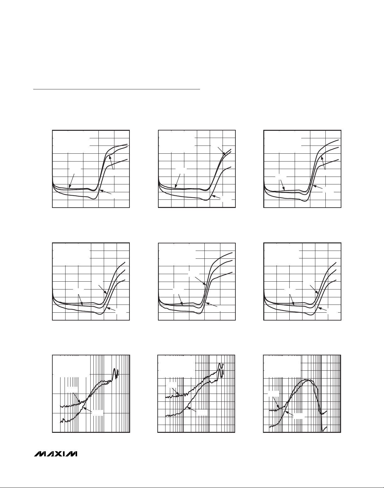
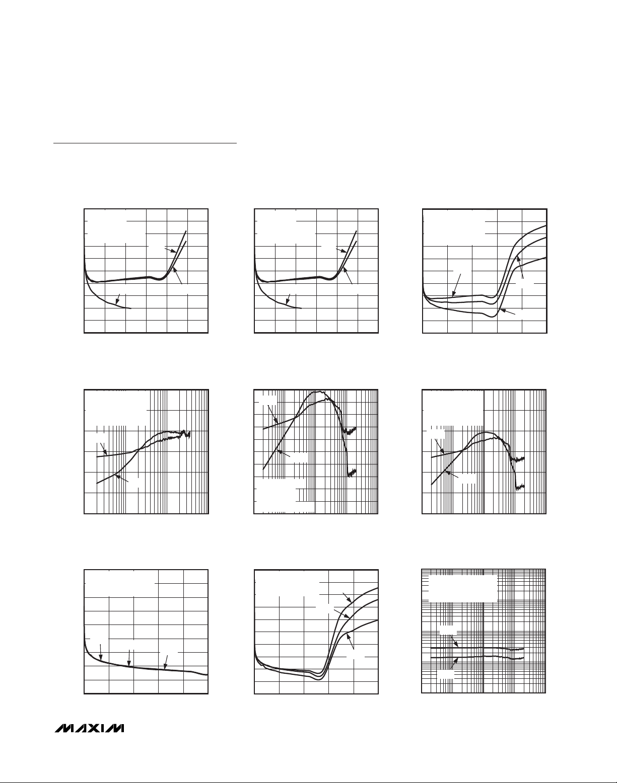
Typical Operating Characteristics
(V
AVDD
= V
PVDD
= V
MICVDD
= V
DVDD
= V
DVDDS1
= +1.8V, RL= ∞, headphone load (RL) connected between _OUTP and _OUTN,
C
REF
= 2.2µF, C
MICBIAS
= C
PREG
= C
REG
= 1µF, AV
PRE
= +20dB, AV
PGAM
= 0dB, AV
DAC
= 0dB, AV
LINE
= +20dB, AV
VOL
= 0dB,
AV
LO
= 0dB, f
MCLK
= 13MHz, differential output, unless otherwise noted.)
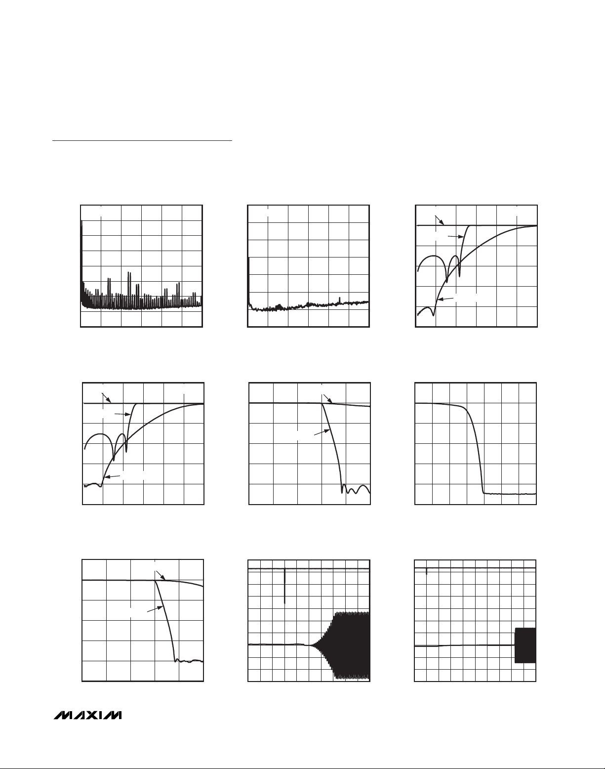
TOTAL HARMONIC DISTORTION + NOISE
vs. POWER OUT (DAC TO HEADPHONE)
0
f
-10
f
R
-20
DIFFERENTIAL MODE
-30
-40
-50
THD+N (dB)
-60
-70
-80
-90
-100
050
TOTAL HARMONIC DISTORTION + NOISE
vs. POWER OUT (DAC TO HEADPHONE)
0
f
-10
f
R
-20
DIFFERENTIAL MODE
-30
-40
-50
THD+N (dB)
-60
-70
-80
-90
-100
060
= 13MHz
MCLK
LRCLK
LOAD
= 12.288MHz
MCLK
LRCLK
LOAD
TOTAL HARMONIC DISTORTION + NOISE
vs. POWER OUT (DAC TO HEADPHONE)
0
f
MCLK
-10
= 8kHz
= 32
Ω
3kHz
MAX9880A toc01
1kHz
20Hz
40302010
POWER OUT (mW)
f
LRCLK
R
LOAD
-20
DIFFERENTIAL MODE
-30
-40
-50
THD+N (dB)
-60
-70
-80
-90
-100
060
TOTAL HARMONIC DISTORTION + NOISE
vs. POWER OUT (DAC TO HEADPHONE)
0
f
MCLK
MAX9880A toc04
-10
f
LRCLK
R
LOAD
-20
DIFFERENTIAL MODE
-30
-40
-50
THD+N (dB)
-60
-70
-80
-90
-100
050
= 48kHz
= 16
Ω
6kHz
1kHz
20Hz
5040302010
POWER OUT (mW)
= 13MHz
= 8kHz
= 16
Ω
3kHz
POWER OUT (mW)
= 12.288MHz
= 96kHz
= 32
Ω
1kHz
6kHz
POWER OUT (mW)
1kHz
20Hz
5040302010
20Hz
40302010
MAX9880A toc02
MAX9880A toc05
TOTAL HARMONIC DISTORTION + NOISE
vs. POWER OUT (DAC TO HEADPHONE)
0
f
= 12.288MHz
MCLK
-10
-20
-30
-40
-50
THD+N (dB)
-60
-70
-80
-90
-100
= 48kHz
f
LRCLK
= 32
R
Ω
LOAD
DIFFERENTIAL MODE
6kHz
050
POWER OUT (mW)
1kHz
20Hz
40302010
TOTAL HARMONIC DISTORTION + NOISE
vs. POWER OUT (DAC TO HEADPHONE)
0
f
= 12.288MHz
MCLK
-10
-20
-30
-40
-50
THD+N (dB)
-60
-70
-80
-90
-100
= 96kHz
f
LRCLK
= 16
R
Ω
LOAD
DIFFERENTIAL MODE
1kHz
6kHz
20Hz
060
POWER OUT (mW)
5040302010
MAX9880A toc03
MAX9880A toc06
TOTAL HARMONIC DISTORTION + NOISE
vs. FREQUENCY (DAC TO HEADPHONE)
-70
f
= 13MHz
MCLK
= 8kHz
f
LRCLK
= 32
R
Ω
LOAD
DIFFERENTIAL MODE
-75
-80
THD+N (dB)
-85
-90
5mW
20mW
10 10,000
FREQUENCY (Hz)
1000100
MAX9880A toc07
TOTAL HARMONIC DISTORTION + NOISE
vs. FREQUENCY (DAC TO HEADPHONE)
-70
f
= 13MHz
MCLK
-72
-74
-76
-78
-80
THD+N (dB)
-82
-84
-86
-88
-90
= 8kHz
f
LRCLK
= 16
R
Ω
LOAD
DIFFERENTIAL MODE
5mW
20mW
10 10,000
FREQUENCY (Hz)
1000100
MAX9880A toc08
TOTAL HARMONIC DISTORTON + NOISE
vs. FREQUENCY (DAC TO HEADPHONE)
-70
f
= 12.288MHz
MCLK
-72
-74
-76
-78
-80
THD+N (dB)
-82
-84
-86
-88
-90
= 48kHz
f
LRCLK
= 32
R
Ω
LOAD
DIFFERENTIAL MODE
5mW
20mW
10 100k
FREQUENCY (Hz)
MAX9880A toc09
10k1k100
MAX9880A
Low-Power, High-Performance
Dual I2S Stereo Audio Codec
16 ______________________________________________________________________________________
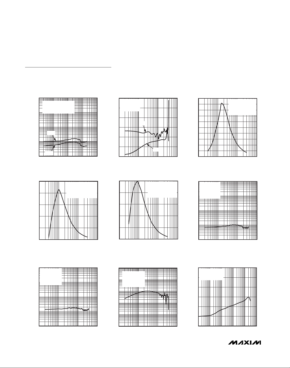
Typical Operating Characteristics (continued)
(V
AVDD
= V
PVDD
= V
MICVDD
= V
DVDD
= V
DVDDS1
= +1.8V, RL= ∞, headphone load (RL) connected between _OUTP and _OUTN,
C
REF
= 2.2µF, C
MICBIAS
= C
PREG
= C
REG
= 1µF, AV
PRE
= +20dB, AV
PGAM
= 0dB, AV
DAC
= 0dB, AV
LINE
= +20dB, AV
VOL
= 0dB,
AV
LO
= 0dB, f
MCLK
= 13MHz, differential output, unless otherwise noted.)
TOTAL HARMONIC DISTORTON + NOISE
vs. FREQUENCY (DAC TO HEADPHONE)
-70
f
MCLK
-72
f
LRCLK
R
-74
DIFFERENTIAL MODE
-76
5mW
-78
-80
THD+N (dB)
-82
-84
-86
-88
-90
10 100k
= 12.288MHz
= 48kHz
= 16
LOAD
TOTAL HARMONIC DISTORTON + NOISE
vs. FREQUENCY (DAC TO HEADPHONE)
-70
f
= 12.288MHz
MCLK
Ω
20mW
FREQUENCY (Hz)
-72
-74
MAX9880A toc10
-76
-78
-80
THD+N (dB)
-82
-84
-86
-88
10k1k100
-90
= 96kHz
f
LRCLK
= 32
R
LOAD
DIFFERENTIAL MODE
5mW
10 100k
Ω
20mW
FREQUENCY (Hz)
10k1k100
MAX9880A toc11
TOTAL HARMONIC DISTORTON + NOISE
vs. FREQUENCY (DAC TO HEADPHONE)
-70
f
= 12.288MHz
MCLK
-72
-74
-76
-78
-80
THD+N (dB)
-82
-84
-86
-88
-90
= 96kHz
f
LRCLK
= 16
R
Ω
LOAD
DIFFERENTIAL MODE
5mW
20mW
10 100k
FREQUENCY (Hz)
MAX9880A toc12
10k1k100
TOTAL HARMONIC DISTORTION + NOISE
vs. POWER OUT (DAC TO HEADPHONE)
0
f
= 13MHz
MCLK
-10
-20
-30
-40
-50
THD+N (dB)
-60
-70
-80
-90
-100
= 8kHz
f
LRCLK
= 32
R
Ω
LOAD
CAPACITORLESS MODE
3kHz
015
POWER OUT (mW)
1kHz
20Hz
105
MAX9880A toc13
TOTAL HARMONIC DISTORTION + NOISE
vs. FREQUENCY (DAC TO HEADPHONE)
-60
f
= 13MHz
MCLK
= 8kHz
f
LRCLK
-65
-70
-75
THD+N (dB)
-80
-85
= 32
R
Ω
LOAD
CAPACITORLESS MODE
1mW
MAX9880A toc16
5mW
TOTAL HARMONIC DISTORTION + NOISE
vs. POWER OUT (DAC TO HEADPHONE)
0
f
= 12.288MHz
MCLK
-10
-20
-30
-40
-50
THD+N (dB)
-60
-70
-80
-90
-100
= 48kHz
f
LRCLK
= 32
R
LOAD
CAPACITORLESS MODE
6kHz
015
TOTAL HARMONIC DISTORTION + NOISE
vs. FREQUENCY (DAC TO HEADPHONE)
-60
f
= 12.288MHz
MCLK
= 48kHz
f
LRCLK
-65
-70
-75
THD+N (dB)
-80
-85
= 32
R
LOAD
CAPACITORLESS MODE
1mW
Ω
POWER OUT (mW)
Ω
5mW
TOTAL HARMONIC DISTORTION + NOISE
vs. POWER OUT (DAC TO HEADPHONE)
0
f
= 12.288MHz
MCLK
-10
-20
MAX9880A toc14
-30
-40
1kHz
20Hz
105
-50
THD+N (dB)
-60
-70
-80
-90
-100
= 96kHz
f
LRCLK
= 32
R
Ω
LOAD
CAPACITORLESS MODE
1kHz
015
POWER OUT (mW)
6kHz
20Hz
105
MAX9880A toc15
TOTAL HARMONIC DISTORTION + NOISE
vs. FREQUENCY (DAC TO HEADPHONE)
-60
f
= 12.288MHz
MCLK
= 96kHz
f
LRCLK
MAX9880A toc17
-65
-70
-75
THD+N (dB)
-80
-85
= 32
R
Ω
LOAD
CAPACITORLESS MODE
5mW
20mW
MAX9880A toc18
-90
10 10,000
FREQUENCY (Hz)
1000100
-90
10 100k
FREQUENCY (Hz)
10k1k100
-90
10 100k
FREQUENCY (Hz)
10k1k100
MAX9880A
Low-Power, High-Performance
Dual I2S Stereo Audio Codec
______________________________________________________________________________________
17
Typical Operating Characteristics (continued)
(V
AVDD
= V
PVDD
= V
MICVDD
= V
DVDD
= V
DVDDS1
= +1.8V, RL= ∞, headphone load (RL) connected between _OUTP and _OUTN,
C
REF
= 2.2µF, C
MICBIAS
= C
PREG
= C
REG
= 1µF, AV
PRE
= +20dB, AV
PGAM
= 0dB, AV
DAC
= 0dB, AV
LINE
= +20dB, AV
VOL
= 0dB,
AV
LO
= 0dB, f
MCLK
= 13MHz, differential output, unless otherwise noted.)
TOTAL HARMONIC DISTORTION + NOISE
vs. POWER OUT (DAC TO HEADPHONE)
-40
f
-45
f
R
-50
SINGLE-ENDED MODE
-55
-60
-65
THD+N (%)
-70
-75
-80
-85
-90
012
TOTAL HARMONIC DISTORTION + NOISE
vs. FREQUENCY (DAC TO HEADPHONE)
-60
f
f
-65
R
SINGLE-ENDED MODE
-70
-75
THD+N (dB)
-80
-85
-90
10 10,000
MCLK
LRCLK
LOAD
MCLK
LRCLK
LOAD
1mW
= 13MHz
= 8kHz
= 32
= 13MHz
= 8kHz
= 32
TOTAL HARMONIC DISTORTION + NOISE
vs. POWER OUT (DAC TO HEADPHONE)
-40
f
MCLK
-45
f
Ω
20Hz
POWER OUT (mW)
MAX9880A toc19
1kHz
3kHz
108642
LRCLK
R
LOAD
-50
SINGLE-ENDED MODE
-55
-60
-65
THD+N (%)
-70
-75
-80
-85
-90
012
TOTAL HARMONIC DISTORTON + NOISE
vs. FREQUENCY (DAC TO HEADPHONE)
-70
1mW
-72
Ω
5mW
1000100
FREQUENCY (Hz)
MAX9880A toc22
-74
-76
-78
-80
THD+N (dB)
-82
-84
f
MCLK
-86
f
LRCLK
R
LOAD
-88
SINGLE-ENDED MODE
-90
10 100k
= 12.288MHz
= 48kHz
= 32
Ω
20Hz
POWER OUT (mW)
5mW
= 12.288MHz
= 48kHz
= 32
Ω
FREQUENCY (Hz)
1kHz
6kHz
108642
10k1k100
MAX9880A toc20
MAX9880A toc23
TOTAL HARMONIC DISTORTION + NOISE
vs. POWER OUT (DAC TO HEADPHONE)
0
-10
-20
-30
-40
-50
THD+N (dB)
-60
-70
-80
-90
-100
015
TOTAL HARMONIC DISTORTION + NOISE
vs. FREQUENCY (DAC TO HEADPHONE)
-60
-65
-70
-75
THD+N (dB)
-80
-85
-90
10 100k
f
= 12.288MHz
MCLK
= 96kHz
f
LRCLK
= 32
R
Ω
LOAD
SINGLE-ENDED MODE
1kHz
POWER OUT (mW)
f
= 12.288MHz
MCLK
= 96kHz
f
LRCLK
= 32
R
Ω
LOAD
SINGLE-ENDED MODE
5mW
20mW
FREQUENCY (Hz)
MAX9880A toc21
6kHz
20Hz
12963
MAX9880A toc24
10k1k100
TOTAL HARMONIC DISTORTION + NOISE
vs. POWER OUT (LINE-IN TO HEADPHONE)
0
LINE-IN PREAMP = +18dB
-10
-20
-30
-40
-50
THD+N (dB)
-60
-70
-80
-90
= 32
R
Ω
LOAD
DIFFERENTIAL MODE
1kHz
6kHz
050
POWER OUT (mW)
20Hz
40302010
MAX9880A toc25
TOTAL HARMONIC DISTORTION + NOISE
vs. POWER OUT (LINE-IN TO HEADPHONE)
0
LINE-IN PREAMP = 0dB
-10
-20
-30
-40
-50
THD+N (dB)
-60
-70
-80
-90
-100
= 32
R
LOAD
DIFFERENTIAL MODE
050
Ω
POWER OUT (mW)
6kHz
1kHz
20Hz
40302010
MAX9880A toc26
TOTAL HARMONIC DISTORTION + NOISE
vs. FREQUENCY (LINE-IN TO HEADPHONE)
10
LINE-IN PREAMP = +18dB
I
= 32
R
LOAD
DIFFERENTIAL MODE
1
0.1
THD+N (%)
0.01
0.001
5mW
20mW
10 100,000
FREQUENCY (Hz)
10,0001000100
MAX9880A toc27
MAX9880A
Low-Power, High-Performance
Dual I
2
S Stereo Audio Codec
18 ______________________________________________________________________________________
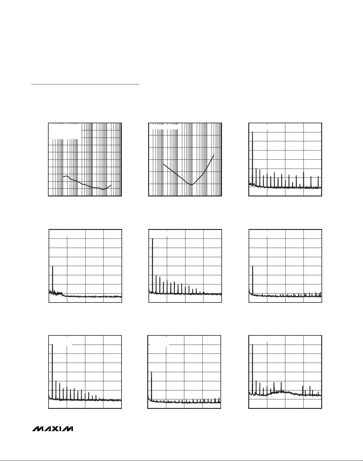
Typical Operating Characteristics (continued)
(V
AVDD
= V
PVDD
= V
MICVDD
= V
DVDD
= V
DVDDS1
= +1.8V, RL= ∞, headphone load (RL) connected between _OUTP and _OUTN,
C
REF
= 2.2µF, C
MICBIAS
= C
PREG
= C
REG
= 1µF, AV
PRE
= +20dB, AV
PGAM
= 0dB, AV
DAC
= 0dB, AV
LINE
= +20dB, AV
VOL
= 0dB,
AV
LO
= 0dB, f
MCLK
= 13MHz, differential output, unless otherwise noted.)
TOTAL HARMONIC DISTORTION + NOISE
vs. FREQUENCY (LINE-IN TO HEADPHONE)
10
1
0.1
THD+N (%)
0.01
0.001
10 100,000
OUTPUT POWER vs. LOAD RESISTANCE
25
20
15
10
POWER OUT (mW)
5
LINE-IN PREAMP = 0dB
I
= 32
R
LOAD
DIFFERENTIAL MODE
5mW
20mW
FREQUENCY (Hz)
(DAC TO HEADPHONE)
f
MCLK
f
LRCLK
THD+N ≤ 0.1%
CAPACITORLESS MODE
10,0001000100
= 12.288MHz
= 48kHz
TOTAL HARMONIC DISTORTION + NOISE
vs. FREQUENCY (DAC TO LINE-OUT)
-30
f
= 13MHz
MCLK
= 8kHz
f
LRCLK
-40
MAX9880A toc28
0dBFS
-50
-60
THD+N (dB)
-70
-80
-90
10 10,000
IIR
FIR
1000100
FREQUENCY (Hz)
POWER OUT vs. HEADPHONE LOAD
MAX9880A toc31
25
20
15
10
POWER OUT (mW)
5
f
= 12.288MHz
MCLK
= 48kHz
f
LRCLK
THD+N ≤ 0.1%
SINGLE-ENDED MODE
MAX9880A toc29
MAX9880A toc32
POWER OUT vs. HEADPHONE LOAD
50
45
40
35
30
25
20
POWER OUT (mW)
15
10
5
0
1 1000
HEADPHONE LOAD (Ω)
f
MCLK
f
LRCLK
THD+N ≤ 0.1%
DIFFERENTIAL MODE
TOTAL HARMONIC DISTORTION + NOISE
vs. FREQUENCY (MICROPHONE TO ADC)
10
f
= 13MHz
MCLK
= 8kHz
f
LRCLK
MICPRE = 0dB
= 1V
V
1
IN
P-P
0.1
THD+N (%)
0.01
= 12.288MHz
= 48kHz
10010
MAX9880A toc30
MAX9880A toc33
0
1 1000
HEADPHONE LOAD (Ω)
10010
TOTAL HARMONIC DISTORTION + NOISE
vs. FREQUENCY (MICROPHONE TO ADC)
10
f
= 13MHz
MCLK
= 8kHz
f
LRCLK
MICPRE = +20dB
= 100mV
V
1
IN
P-P
0.1
THD+N (%)
0.01
0.001
10 10,000
FREQUENCY (Hz)
1000100
MAX9880A toc34
0
1 1000
HEADPHONE LOAD (Ω)
10010
TOTAL HARMONIC DISTORTION + NOISE
vs. FREQUENCY (MICROPHONE TO ADC)
100
f
= 13MHz
MCLK
= 8kHz
f
LRCLK
10
MICPRE = +30dB
VIN = 32mV
P-P
1
THD+N (%)
0.1
0.01
0.001
10 10,000
FREQUENCY (Hz)
1000100
MAX9880A toc35
0.001
10 10,000
FREQUENCY (Hz)
POWER-SUPPLY REJECTION RATIO
vs. FREQUENCY (DAC TO HEADPHONE)
0
f
= 12.288MHz
MCLK
= 48kHz
f
LRCLK
-20
-40
-60
PSRR (dB)
-80
-100
-120
= 100mV
V
RIPPLE
1 100k
P-P
FREQUENCY (Hz)
1000100
MAX9880A toc36
10k1k10010
MAX9880A
Low-Power, High-Performance
Dual I2S Stereo Audio Codec
______________________________________________________________________________________
19
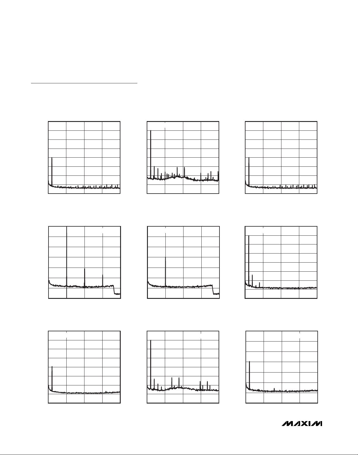
Typical Operating Characteristics (continued)
(V
AVDD
= V
PVDD
= V
MICVDD
= V
DVDD
= V
DVDDS1
= +1.8V, RL= ∞, headphone load (RL) connected between _OUTP and _OUTN,
C
REF
= 2.2µF, C
MICBIAS
= C
PREG
= C
REG
= 1µF, AV
PRE
= +20dB, AV
PGAM
= 0dB, AV
DAC
= 0dB, AV
LINE
= +20dB, AV
VOL
= 0dB,
AV
LO
= 0dB, f
MCLK
= 13MHz, differential output, unless otherwise noted.)
POWER-SUPPLY REJECTION RATIO
vs. FREQUENCY (MICROPHONE TO ADC)
0
V
= 100mV
RIPPLE
-10
f
MCLK
f
LRCLK
-20
-30
-40
-50
PSRR (dB)
-60
-70
-80
-90
-100
1 100k
= 12.288MHz
= 48kHz
FREQUENCY (Hz)
P-P
FFT, DAC TO HEADPHONE,
-60dBFS, f
20
FREQ1 = 0xA
0
-20
-40
-60
-80
AMPLITUDE (dB)
-100
-120
-140
0 20k
= 13MHz, f
MCLK
FREQUENCY (Hz)
LRCLK
15k10k5k
10k1k10010
= 8kHz
MAX9880A toc37
PSRR (dB)
-100
-120
MAX9880A toc40
AMPLITUDE (dB)
-100
-120
-140
POWER-SUPPLY REJECTION RATIO
vs. FREQUENCY (MICBIAS)
0
V
= 100mV
RIPPLE
-20
-40
-60
-80
1 100k
P-P
10k1k10010
FREQUENCY (Hz)
FFT, DAC TO HEADPHONE,
0dBFS, f
20
NI = 0x6000
0
-20
-40
-60
-80
0 20k
= 12.288MHz, f
MCLK
FREQUENCY (Hz)
LRCLK
15k10k5k
= 48kHz
MAX9880A toc38
MAX9880A toc41
FFT, DAC TO HEADPHONE,
0dBFS, f
20
FREQ1 = 0xA
0
-20
-40
-60
-80
AMPLITUDE (dB)
-100
-120
-140
020k
= 13MHz, f
MCLK
FREQUENCY (Hz)
FFT, DAC TO HEADPHONE,
-60dBFS, f
20
NI = 0x6000
0
-20
-40
-60
-80
AMPLITUDE (dB)
-100
-120
-140
0 20k
= 12.288MHz, f
MCLK
FREQUENCY (Hz)
LRCLK
= 8kHz
15k10k5k
LRCLK
15k10k5k
MAX9880A toc39
= 48kHz
MAX9880A toc42
FFT, DAC TO HEADPHONE,
MCLK
NI = 0x6000
DHF = 1
= 12.288MHz, f
FREQUENCY (Hz)
0dBFS, f
20
0
-20
-40
-60
-80
AMPLITUDE (dB)
-100
-120
-140
0 20k
LRCLK
15k10k5k
= 96kHz
MAX9880A toc43
FFT, DAC TO HEADPHONE,
-60dBFS, f
20
NI = 0x6000
DHF = 1
0
-20
-40
-60
-80
AMPLITUDE (dB)
-100
-120
-140
0 20k
= 12.288MHz, f
MCLK
FREQUENCY (Hz)
LRCLK
15k10k5k
= 96kHz
MAX9880A toc44
FFT, DAC TO HEADPHONE,
0dBFS, f
20
PLL MODE
0
-20
-40
-60
-80
AMPLITUDE (dB)
-100
-120
-140
020k
= 13MHz, f
MCLK
FREQUENCY (Hz)
LRCLK
15k10k5k
= 48kHz
MAX9880A toc45
MAX9880A
Low-Power, High-Performance
Dual I2S Stereo Audio Codec
20 ______________________________________________________________________________________
Typical Operating Characteristics (continued)
(V
AVDD
= V
PVDD
= V
MICVDD
= V
DVDD
= V
DVDDS1
= +1.8V, RL= ∞, headphone load (RL) connected between _OUTP and _OUTN,
C
REF
= 2.2µF, C
MICBIAS
= C
PREG
= C
REG
= 1µF, AV
PRE
= +20dB, AV
PGAM
= 0dB, AV
DAC
= 0dB, AV
LINE
= +20dB, AV
VOL
= 0dB,
AV
LO
= 0dB, f
MCLK
= 13MHz, differential output, unless otherwise noted.)
-60dBFS, f
20
PLL MODE
0
-20
-40
-60
-80
AMPLITUDE (dB)
-100
-120
-140
0 20k
FFT, DAC TO HEADPHONE,
= 13MHz, f
MCLK
FREQUENCY (Hz)
LRCLK
15k10k5k
= 48kHz
MAX9880A toc46
AMPLITUDE (dB)
-100
-120
-140
FFT, DAC TO HEADPHONE,
0dBFS, f
20
PLL MODE
0
-20
-40
-60
-80
0 20k
= 13MHz, f
MCLK
FREQUENCY (Hz)
LRCLK
= 44.1kHz
15k10k5k
MAX9880A toc47
FFT, DAC TO HEADPHONE,
-60dBFS, f
20
PLL MODE
0
-20
-40
-60
-80
AMPLITUDE (dB)
-100
-120
-140
020k
= 13MHz, f
MCLK
FREQUENCY (Hz)
LRCLK
15k10k5k
= 44.1kHz
MAX9880A toc48
FFT, MICROPHONE TO ADC,
0dBFS, f
0
-20
-40
-60
-80
AMPLITUDE (dB)
-100
-120
-140
0 4000
= 13MHz, f
MCLK
FREQUENCY (Hz)
FFT, MICROPHONE TO ADC,
-60dBFS, f
20
NI = 0x6000
0
-20
-40
-60
-80
AMPLITUDE (dB)
-100
-120
-140
0 20k
= 12.288MHz, f
MCLK
FREQUENCY (Hz)
LRCLK
FREQ1 = 0xA
300020001000
LRCLK
15k10k5k
= 8kHz
= 48kHz
MAX9880A toc49
MAX9880A toc52
FFT, MICROPHONE TO ADC,
-60dBFS, f
0
FREQ1 = 0xA
-20
-40
-60
-80
AMPLITUDE (dB)
-100
-120
-140
0 4000
= 13MHz, f
MCLK
FREQUENCY (Hz)
FFT, MICROPHONE TO ADC,
0dBFS, f
20
0
-20
-40
-60
-80
AMPLITUDE (dB)
-100
-120
-140
0 20k
= 13MHz, f
MCLK
FREQUENCY (Hz)
LRCLK
LRCLK
300020001000
= 48kHz
PLL MODE
15k10k5k
= 8kHz
MAX9880A toc50
MAX9880A toc53
FFT, MICROPHONE TO ADC,
0dBFS, f
20
NI = 0x6000
0
-20
-40
-60
-80
AMPLITUDE (dB)
-100
-120
-140
020k
= 12.288MHz, f
MCLK
FREQUENCY (Hz)
LRCLK
15k10k5k
= 48kHz
MAX9880A toc51
FFT, MICROPHONE TO ADC,
-60dBFS, f
0
-20
-40
-60
-80
AMPLITUDE (dB)
-100
-120
-140
0 20k
= 13MHz, f
MCLK
FREQUENCY (Hz)
LRCLK
PLL MODE
15k10k5k
= 48kHz
MAX9880A toc54
MAX9880A
Low-Power, High-Performance
Dual I2S Stereo Audio Codec
______________________________________________________________________________________
21
Typical Operating Characteristics (continued)
(V
AVDD
= V
PVDD
= V
MICVDD
= V
DVDD
= V
DVDDS1
= +1.8V, RL= ∞, headphone load (RL) connected between _OUTP and _OUTN,
C
REF
= 2.2µF, C
MICBIAS
= C
PREG
= C
REG
= 1µF, AV
PRE
= +20dB, AV
PGAM
= 0dB, AV
DAC
= 0dB, AV
LINE
= +20dB, AV
VOL
= 0dB,
AV
LO
= 0dB, f
MCLK
= 13MHz, differential output, unless otherwise noted.)
WIDEBAND FFT, DAC TO HEADPHONE,
0dBFS, f
20
FREQ1 = 0xA
0
-20
-40
-60
-80
AMPLITUDE (dB)
-100
-120
-140
0 120k
= 13MHz, f
MCLK
FREQUENCY (Hz)
ADC IIR HIGHPASS FILTER FREQUENCY
RESPONSE, MODE = 0
20
AVFLT = 0
0
AVFLT = 3
-20
-40
AMPLITUDE (dB)
-60
-80
AVFLT = 4
LRCLK
f
LRCLK
= 8kHz
100k80k20k 40k 60k
= 8kHz
MAX9880A toc55
AMPLITUDE (dB)
-100
-120
-140
MAX9880A toc58
AMPLITUDE (dB)
WIDEBAND FFT, DAC TO HEADPHONE,
-60dBFS, f
0
FREQ1 = 0xA
-20
-40
-60
-80
0 120k
= 13MHz, f
MCLK
FREQUENCY (Hz)
LRCLK
100k80k60k40k20k
DAC IIR/FIR LOWPASS FILTER FREQUENCY
LRCLK
MODE = 1
= 8kHz)
-20
-40
-60
-80
20
RESPONSE (f
0
MODE = 0
= 8kHz
MAX9880A toc56
MAX9880A toc59
DAC IIR HIGHPASS FILTER FREQUENCY
RESPONSE, MODE = 0
20
DVFLT = 0
0
DVFLT = 3
-20
-40
AMPLITUDE (dB)
-60
-80
-100
0 600
DVFLT = 4
FREQUENCY (Hz)
DAC FIR LOWPASS FILTER FREQUENCY
RESPONSE (f
20
0
-20
-40
AMPLITUDE (dB)
-60
-80
LRCLK
f
LRCLK
= 96kHz)
= 8kHz
MAX9880A toc57
500400300200100
MAX9880A toc60
-100
0 600
FREQUENCY (Hz)
ADC IIR/FIR LOWPASS FILTER FREQUENCY
20
RESPONSE (f
0
-20
-40
AMPLITUDE (dB)
-60
-80
-100
3000 4000
MODE = 0
FREQUENCY (Hz)
LRCLK
MODE = 1
= 8kHz)
MAX9880A toc62
-100
20k 48k
FREQUENCY (Hz)
SHUTDOWN TO FULL OPERATION
(SE CLICKLESS)
SCL (1V/div)LOUTP (500mV/div)
TIME (40ms/div)
44k40k36k32k28k24k
MAX9880A toc63
500400300200100
-100
3000 4000
FREQUENCY (Hz)
3800360034003200
SHUTDOWN TO FULL OPERATION
(DIFFERENTIAL)
MAX9880A toc61
SCL (1V/div)LOUTP (500mV/div)
3800360034003200
TIME (4ms/div)

MAX9880A
Low-Power, High-Performance
Dual I2S Stereo Audio Codec
22 ______________________________________________________________________________________
Typical Operating Characteristics (continued)
(V
AVDD
= V
PVDD
= V
MICVDD
= V
DVDD
= V
DVDDS1
= +1.8V, RL= ∞, headphone load (RL) connected between _OUTP and _OUTN,
C
REF
= 2.2µF, C
MICBIAS
= C
PREG
= C
REG
= 1µF, AV
PRE
= +20dB, AV
PGAM
= 0dB, AV
DAC
= 0dB, AV
LINE
= +20dB, AV
VOL
= 0dB,
AV
LO
= 0dB, f
MCLK
= 13MHz, differential output, unless otherwise noted.)
SHUTDOWN TO FULL OPERATION
(SE FAST TURN ON)
FULL OPERATION TO SHUTDOWN
SOFT-START ADC
SCL (1V/div)LOUTP (500mV/div)
TIME (4ms/div)
TOTAL HARMONIC DISTORTION + NOISE
0
-10
-20
-30
-40
-50
THD+N (dB)
-60
-70
-80
-90
-100
10 100
MAX9880A toc64
vs. MCLK FREQUENCY, 0dBFS
f
= 48kHz
LRCLK
PLL MODE
MCLK FREQUENCY (MHz)
SCL (1V/div)LOUTP (500mV/div)
MAX9880A toc67
TIME (400µs/div)
MAX9880A toc65
SCL (1V/div)ADC OUTPUT (500mV/div)
DYNAMIC RANGE vs. MCLK FREQUENCY
120
VIN = -60dBFS
= 48kHz
f
LRCLK
110
PLL MODE
100
90
80
DYNAMIC RANGE (dB)
70
60
10 100
MCLK FREQUENCY (MHz)
MAX9880A toc66
TIME (1ms/div)
MAX9880A toc68
LINE INPUT RESISTANCE
300
vs. GAIN SETTING
250
200
150
100
INPUT RESISTANCE (kΩ)
50
0
-10 25
GAIN SETTING (dB)
30,000
MAX9880A toc69
20151050-5
25,000
20,000
15,000
10,000
5000
AUX CODE (SIGNED DECIMAL)
-5000
AUX CODE vs. INPUT VOLTAGE
0
-0.4 1.2
INPUT VOLTAGE (V)
1.00.80.60.40.20-0.2
MAX9880A toc70

MAX9880A
Low-Power, High-Performance
Dual I2S Stereo Audio Codec
______________________________________________________________________________________ 23
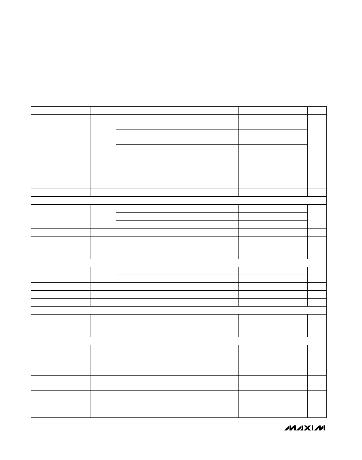
Pin Configurations
TOP VIEW
(BUMP SIDE DOWN)
+
A
B
C
D
E
F
MAX9880A
1
234
X2X1DGND AGNDPREGAVDDMODE
IRQ
CSSCL/SCLKSDA/DINDVDD MICBIASMICVDDREFDOUT
N.C.BCLKS2LRCLKS2SDINS2
N.C.SDINS1SDOUTS2MCLK
LOUTPPVDDBCLKS1LRCLKS1 LINLLOUTLPGNDROUTP
LOUTNPVDDDVDDS1SDOUTS1 LINRLOUTRPGNDROUTN
JACKSNS/
5678
MICRP/
SPDMDATA
MICRN/
SPDMCLK
AUX
REGN.C.
N.C.
MICLN/
DIGMICCLK
MICLP/
DIGMICDATA
WLP
TOP VIEW
37
SDOUTS1
38
SDINS1
39
LRCLKS1
40
BCLKS1
41
MCLK
42
SDOUTS2
43
SDINS2
44
LRCLKS2
45
BCLKS2
46
DVDD
47
DGND
48
N.C.
*EP = EXPOSED PAD
N.C.
N.C.
PVDD
DVDDS1
35
34 33 32 31 30 29 28 272625
36
LOUTN
LOUTP
MAX9880A
ROUTN
+
1
SDA/DIN
2
345
X1
SCL/SCLK
6789101112
X2
CS
DOUT
MODE
THIN QFN
× 6mm)
(6mm
ROUTP
IRQ
N.C.
AVDD
PGND
*EP
REF
LOUTL
N.C.
LOUTR
24
LINR
23
LINL
22
JACKSNS/AUX
21
MICRN/SPDMCLK
20
MICRP/SPDMDATA
19
MICLP/DIGMICDATA
18
MICLN/DIGMICCLK
17
MICBIAS
16
MICVDD
15
AGND
14
N.C.
13
REG
PREG

MAX9880A
Low-Power, High-Performance
Dual I
2
S Stereo Audio Codec
24 ______________________________________________________________________________________
Pin Description
PIN
TQFN-EP WL P
1 B2 SDA/DIN
2 B3 SCL/SCLK
3 A2 X1
4 A3 X2
5 B4 CS SPI-Compatible, Active-Low Chip-Select Input
6 B5 DOUT SPI-Compatible Serial-Data Output
7 A5 MODE I2C/SPI Mode Select Input (MODE = 0 for I2C mode, MODE = 1 for SPI mode)
8 A4 IRQ
9 A6 AVDD Analog Power Supply. Bypass to AGND with a 1µF capacitor.
10 B6 REF Converter Reference. Bypas s to AGND with a 2.2µF capacitor (1.23V nominal).
11, 14,
28, 33,
35, 48
12 A7 PREG
13 C6 REG
15 A8 AGND Analog Ground
16 B7 MICVDD Microphone Bias Power Supply. Bypass to AGND with a 1µF capacitor.
17 B8 MICBIAS
18 C7
19 D7
20 C8
21 D8
22 D5 JACKSNS/AUX
C4, D4,
C5, D6
NAME FUNCTION
2
I
C Serial-Data Input/Output (MODE = 0). Connect a pul lup resistor to DVDD for
full output swing. SPI compatible serial-data input (MODE = 1).
2
I
C Serial-Clock Input (MODE = 0). Connect a pullup resi stor to DVDD for full
output swing. SPI-compatible serial clock input (MODE = 1).
Crystal Osc illator Input. Connect load capacitor and one terminal of the cr ystal
to this pin. Acceptable input frequency range: 10MHz to 30MHz.
Crystal Osc illator Output. Connect load capacitor and second terminal of the
crystal to this pin.
Hardware Interrupt Output. IRQ can be programmed to go low when b its in the
status register 0x00 are set. Read status register 0x00 to clear IRQ once set.
Repeat faults have no effect on IRQ until it is cleared by reading the I
register 0x00. Connect a 10k pullup resistor to DVDD for ful l output swing.
N.C. No Connection. Connect to GND.
Positive Internal Regulated Supply. Bypass to AGND with a 1µF capacitor (1.6V
nominal).
PREG/2 Voltage Reference. Bypass to AGND with a 1µF capacitor (0.8V
nominal)
Low-Noi se Microphone B ia s. Connect a 2.2 k to 470 resistor to the pos it ive
output of the microphone. B ypass to AGND with a 1µF capacitor.
MICLN/
DIGMICCLK
MICLP/
DIGMICDATA
MICRP/
SPDMDATA
MICRN/
SPDMCL K
Left Negative Differential Microphone Input. AC-couple a microphone with a series
1µF capacitor. Also digital microphone clock output. Selectable through I
Left Positive Differential Microphone Input. AC-couple a microphone with a
series 1µF capac itor. Also digital microphone data input. Selectable through
2
C.
I
Right Posit ive Different ia l Microphone Input or SPDM Data Output. AC-couple a
microphone with a series 1µF capac itor. Selectable through I
Right Negative Differential Microphone Input or SPDM Cloc k Output. AC-couple
a microphone with a series 1µF capac itor. Selectable through I
Jack Sense. Detects the presence or absence of a jack. See the Headset
Detection section. When used as an auxiliary ADC input, AUX is used to
measure DC vo ltages.
2
C status
2
C.
2
C.
2
C.

MAX9880A
Low-Power, High-Performance
Dual I2S Stereo Audio Codec
______________________________________________________________________________________ 25
Pin Description (continued)
PIN
TQFN-EP WL P
23 E8 LINL Left-Line Input. AC-couple ana log audio s ignal to LINL with a 1µF capacitor.
24 F8 LINR Right-Line Input. AC-couple analog audio signa l to LINR with a 1µF capacitor.
25 F7 LOUTR Right-Line Output
26 E7 LOUTL Left-Line Output
27 E6, F6 PGND Headphone Power Ground
29 E5 ROUTP
30 F5 ROUTN
31 F4 LOUTN
32 E4 LOUTP
34 E3, F3 PVDD Headphone Power Supply. Bypas s to PGND with a 1µF capacitor.
36 F2 DVDDS1
37 F1 SDOUTS1 S1 Digital Audio Serial-Data ADC Output
38 D3 SDINS1 S1 Digital Audio Serial-Data DAC Input
39 E1 LRCLKS1
40 E2 BCLKS1
41 D1 MCLK Master Cloc k Input. Acceptable input frequency range: 10MHz to 60MHz.
42 D2 SDOUTS2 S2 Digital Audio Serial-Data ADC Output
43 C1 SDINS2 S2 Digital Audio Serial-Data DAC Input
44 C2 LRCLKS2
45 C3 BCLKS2
46 B1 DVDD
47 A1 DGND Digital Ground
— — EP Exposed Pad. Connect the exposed thermal pad to AGND.
NAME FUNCTION
Positive Right-Channel Headphone Output. Connect directly to the load in
differential and capacitorless mode. AC-couple to the load in single-ended mode.
Negative Right-Channel Headphone Output. Unu sed in capacitorless and
single-ended mode.
Negative Left-Channel Headphone Output. Common headphone return in
capacitorless mode. Unused in s ingle-ended mode.
Positi ve Left-Channel Headphone Output. Connect directly to the load in
differential and capacitorless mode. AC-couple to the load in single-ended mode.
S1 Digital Audio Interface Power-Supply Input. Bypass to DGND with a 1µF
capacitor.
S1 Digital Aud io Left-Right Clock Input/Output. LRCLKS1 is the audio sample
rate clock and determines whether the audio data on SDINS1 i s routed to the left
or right channel. In TDM mode, LRCLKS1 is a frame sync pulse. LRCLKS1 is an
input when the MAX9880A is in slave mode and an output when in master
mode.
S1 Digital Audio Bit Clock Input/Output. BCLKS1 i s an input when the
MAX9880A is in slave mode and an output when in master mode.
S2 Digital Aud io Left-Right Clock Input/Output. LRCLKS2 is the audio sample
rate clock and determines whether the audio data on SDINS2 i s routed to the left
or right channel. In TDM mode, LRCLKS2 is a frame sync pulse. LRCLKS2 is an
input when the MAX9880A is in slave mode and an output when in master
mode.
S2 Digital Audio Bit Clock Input/Output. BCLKS2 i s an input when the
MAX9880A is in slave mode and an output when in master mode.
Digital Power Supply. Supply for the d igital core and I
DGND with a 1.0µF capacitor.
2
C/SPI interface. Bypass to

MAX9880A
Low-Power, High-Performance
Dual I2S Stereo Audio Codec
26 ______________________________________________________________________________________
Detailed Description
The MAX9880A is a low-power stereo audio codec
designed for portable applications requiring minimum
power consumption.
The stereo playback path accepts digital audio through
flexible digital audio interfaces compatible with I2S,
TDM, and left-justified audio signals. The MAX9880A
can process two simultaneous digital input streams that
can be mixed digitally. The primary interface is intended for voiceband applications, while the secondary
interface can be used for stereo audio data. An oversampling sigma-delta DAC converts the mixed incoming digital data stream to analog audio and outputs
through the stereo headphone amplifier and stereo-line
outputs. The headphone amplifier can be configured in
differential, single-ended, and capacitorless output
modes.
The stereo record path has two differential analog
microphone inputs with selectable gain. The microphones are powered by an integrated microphone bias.
The MAX9880A can retask the left analog microphone
input to accept data from up to two digital microphones. An oversampling sigma-delta ADC converts
the microphone signals and outputs the digital bit
stream over the digital audio interface. An auxiliary
ADC allows accurate measurements of DC voltages by
retasking the right audio ADC. DC voltages can be
read through the registers.
The MAX9880A also includes two line inputs. These
inputs allow a stereo single-ended signal to be gain
adjusted and then recorded by the ADCs and output by
the headphone amplifier and line output amplifiers. A
jack detection function allows the detection of headphone, microphone, and headset jacks. Insertion and
removal events can be programmed to trigger a hardware interrupt and flag a register bit.
The MAX9880A’s flexible clock circuitry utilizes a programmable clock divider and a digital PLL to allow the
DAC and ADC to operate at maximum dynamic range
for all combinations of master clock (MCLK) and sample rate (LRCLK) without consuming extra supply current. Any master clock between 10MHz and 60MHz is
supported as are all sample rates from 8kHz to 48kHz
for the record path and 8kHz to 96kHz for the playback
path. Master and slave modes are supported for maximum flexibility.
The right analog microphone input can be retasked to
output SPDM data. Integrated digital filtering provides a
range of notch and highpass filters for both the playback and record paths to limit undesirable low-frequency signals and GSM transmission noise. The digital
filtering provides attenuation of out-of-band energy by
over 70dB, eliminating audible aliasing. A digital
sidetone function allows audio from the record path to
be summed into the playback path after digital filtering.
I2C/SPI Registers
Forty internal registers program and report the status of
the MAX9880A. Table 1 lists all of the registers, their
addresses, and power-on-reset states. Registers
0x00–0x03 are read-only while all of the other registers
are read/write. Write zeros to all unused bits in the register table when updating the register, unless otherwise
noted. All bits in the read-only registers are not programmable. Read operations of unused bits return zero.
I2C Slave Address
The MAX9880A is preprogrammed with a slave
address of 0x20 or 0010000. The address is defined as
the 7 most significant bits (MSBs) followed by the
read/write bit. Set the read/write bit to 1 to configure the
MAX9880A to read mode. Set the read/write bit to zero
to configure the MAX9880A to write mode. The address
is the first byte of information sent to the MAX9880A
after the START (S) condition.
Table 1. Register Map
REGISTER B7 B6 B5 B4 B3 B2 B1 B0
STATUS
Status CLD SLD ULK — * * JDET — 0x00 — R
Jac k Status JKSNS[1:0] — — — — — — 0x01 — R
AUX High AUX[15:8] 0x02 — R
AUX Low AUX[7:0] 0x03 — R
Interrupt Enable ICLD ISLD IULK 0 0* 0* IJDET 0 0x04 0x00 R/W
SYSTEM CLOCK CONTROL
System Clock 0 0 PSCLK FREQ1 0x05 0x00 R/W
REGISTER
ADDRESS
(SEE NOTE)
POR
STATE
R/W

MAX9880A
Low-Power, High-Performance
Dual I2S Stereo Audio Codec
______________________________________________________________________________________ 27
Table 1. Register Map (continued)
REGISTER B7 B6 B5 B4 B3 B2 B1 B0
DAI1 CLOCK CONTROL
Stereo Audio Clock Control High PLL1 NI1[14:8] 0x06 0x00 R/W
Stereo Audio Clock Control Low NI1[7:1] RLK1/NI1[0] 0x07 0x00 R/W
DAI1 CONFIGURATION
In t e r fac e M o d e A MA S 1 W C I1 B C I 1 DLY1 HIZOFF1 T D M 1 F SW 1 0 0x08 0x00 R/W
Interface M ode B DL1 SEL1 SDOEN1 SDIEN1 DMONO1 BSEL1 0x09 0x00 R/W
Time-Divi sion Multiplex SLOTL1 SLOTR1 SLOTDLY1[3:0] 0x0 A 0x00 R/W
DAI2 CLOCK CONTROL
Stereo Audio Clock Control High PLL2 NI2[14:8] 0x0B 0x00 R/W
Stereo Audio Clock Control Low NI2[7:1] RLK2/NI2[0] 0x0C 0x00 R/W
DAI2 CONFIGURATION
In t e r fac e M o d e A MA S 2 W C I2 B C I 2 DLY2 HIZOFF2 T D M 2 F SW 2 WS2 0 x 0 D 0 x 0 0 R / W
Interface M ode B DL2 SEL2 SDOEN2 SDIEN2 DHF BSEL2 0x0E 0x00 R/W
Time-Divi sion Multiplex SLOTL2 SLOTR2 SLOTDLY2[3:0] 0x0F 0x00 R/W
DIGITAL MIXERS
DAC-L/R Mixer MIXDAL MIXDAR 0x10 0x00 R/W
DIGITAL FILTERING
Codec Filters MODE AVFLT DCB DVFLT 0x11 0x00 R/W
SPDM OUTPUTS
Configuration SPDMCLK SPDML SPDMR 0 0 0 0 0x12 0x00 R/W
Input MIXSPDML MIXSPDMR 0x13 0x00 R/W
REVISION ID
Rev ID location (replicated for
SPI mode)
LEVEL CONTROL
Sidetone DSTS 0 DVST 0x15 0x00 R/W
Stereo DAC Leve l 0 SDACM 0 0 SDACA 0x16 0x00 R/W
Voice DAC Le ve l 0 VDACM VDACG VDACA 0x17 0x00 R/W
Left ADC Le ve l 0 0 AVLG AVL 0x18 0x00 R/W
Right ADC Level 0 0 AVRG AVR 0x19 0x00 R/W
Left-Line Input Level 0 LILM 0 0 LIGL 0x1A 0x00 R/W
Right-Line Input Le ve l 0 LIRM 0 0 LIGR 0x1B 0x00 R/W
Left Volume Control 0 VOLLM VOLL 0x1C 0x00 R/W
Right Volume Control 0 VOLRM VOLR 0x1D 0x00 R/W
Left-Line Output Level 0 LOLM 0 0 LOGL 0x1E 0x00 R/W
Right-Line Output Level 0 LORM 0 0 LOGR 0x1F 0x00 R/W
Left Microphone Gain 0 PALEN PGAML 0x20 0x00 R/W
Right Micropho ne Gain 0 PAREN PGAMR 0x21 0x00 R/W
CONFIGURATION
In p u t MXINL M X I N R AUXCAP AUXGAIN AUXCAL AUX E N 0 x 22 0 x0 0 R/ W
Micropho ne MICCLK DIGMICL DIGMICR 0 0 0 MBIAS 0x23 0x00 R/W
Mode DSLEW VSEN ZDEN 0 0 HPMODE 0x24 0x00 R/W
Jack De tect JDETEN 0 JDWK 0 0 0 JDEB 0x25 0x00 R/W
REV 0x14 0x42 R/W
REGISTER
ADDRESS
(SEE NOTE)
POR
STATE
R/W

MAX9880A
Low-Power, High-Performance
Dual I2S Stereo Audio Codec
28 ______________________________________________________________________________________
Device Status
Status registers 0x00 and 0x01 are read-only registers
that report the status of various device functions. The
status register bits are cleared upon reading the status
register and are set the next time the event occurs.
Registers 0x02 and 0x03 report the DC level applied to
AUX. See the
ADC
section for more details.
Bits in status register 0x00 are set when an alert condition exists. All bits in status register 0x00 are automatically cleared upon a read operation of the register and
are set again if the condition remains or occurs following the read of this register.
Table 1. Register Map (continued)
*
Reserved.
Grayed boxes = Not used.
Note: Register addresses listed are for I
2
C. To get the SPI address, add 0x200 with the following exception: Register 0xFF is not
accessible through SPI.
Table 2. Status Register
*
Reserved.
Grayed boxes = Not used.
Note: Register addresses listed are for I
2
C. To get the SPI address, add 0x200 with the following exception: Register 0xFF is not
accessible through SPI.
REGISTER B7 B6 B5 B4 B3 B2 B1 B0
POWER MANAGEMENT
Enable LNLEN LNREN LOLEN LOREN DALEN DAREN ADLEN ADREN 0x26 0x00 R/W
System Shutdown SHDN 0 0 0 XTEN XTOSC 0 0 0x27 0x00 R/W
REVISION ID
Revision ID REV 0xFF 0x42 R/W
REGISTER
ADDRESS
(SEE NOTE)
POR
STATE
R/W
REGISTER
REGISTER B7 B6 B5 B4 B3 B2 B1 B0
Status CLD SLD ULK — * * JDET — 0x00
Jac k Status JKSNS[1:0] — — — — — — 0x01
AUX High AUX[15:8] 0x02
AUX Low AUX[7:0] 0x03
ADDRESS
(SEE NOTE)

MAX9880A
Low-Power, High-Performance
Dual I
2
S Stereo Audio Codec
______________________________________________________________________________________ 29
Table 3. Status Register Bits
BITS FUNCTION
Clip Detect Flag. Indicates that a signal has become clipped in the ADC or DAC. To resolve a clip condition in
CLD
SLD
ULK
JDET
JKSNS[1:0]
AUX
the signal path, the DAC gain settings and analog input gain settings should be lowered. As the CLD bit does
not indicate where the overload ha s occurred, identify the source by lowering gains individua lly.
Slew Level Detect Flag. When volume or gain changes are made, the slewing circuitry smoothly steps through
all intermediate settings. When SLD is set high, all slewing has completed and the volume or gain is at its final
value. SLD is also set when soft start or stop is complete.
Digital PLL Unlock Flag. Indicates that the digital audio PLL has become unlocked and digital signal data is not
reliable.
Headset Configuration Change Flag. JDET reports changes in JKSNS[1:0]. Changes to JKSNS[1:0] are
debounced before setting JDET. The debounce period is programmable u sing the JDEB bits.
JKSNS reports the status of the JACKSNS pin when JDETEN = 1. JKSNS is not debounced and should be
interpreted according to the following information.
JKSNS[1:0] DESCRIPTION
00 JACKSNS is below V
01 JACKSNS is between V
10 Inval id.
11 JACKSNS is above V
Auxiliary Input Measur ement. AUX is a 16-bit signed two’s complement number representing the voltage
measured at JACKSNS/AUX. Before reading a value from AUX, set AUXCAP to 1 to ensure a stab le reading. After
reading the value, set AUXCAP to 0.
Use the following formula to convert the AUX value into an equivalent JACKSNS/AUX voltage:
Volt age = 0.738V
k = AUX value when AUXGAIN = 1. See AUXGAIN for details on determining the value of k, the calibration
constant.
AUX
k
.
TH2
and V
TH1
.
TH1
TH2
.

MAX9880A
Low-Power, High-Performance
Dual I2S Stereo Audio Codec
30 ______________________________________________________________________________________
Hardware Interrupts
Hardware interrupts are reported on the open-drain IRQ
pin. When an interrupt occurs, IRQ remains low until the
interrupt is serviced by reading the status register 0x00.
If a flag is set, it is reported as a hardware interrupt only
if the corresponding interrupt enable is set. Each bit
enables interrupts for the status flag in the respective
bit location in register 0x00.
Table 4. Interrupt Enable
*
Reserved.
Grayed boxes = Not used.
Note: Register addresses listed are for I
2
C. To get the SPI address, add 0x200 with the following exception: Register 0xFF is not
accessible through SPI.
Table 5. System and Audio Clock Registers
Grayed boxes = Not used.
Note: Register addresses listed are for I
2
C. To get the SPI address, add 0x200 with the following exception: Register 0xFF is not
accessible through SPI.
Clock Control
The MAX9880A can work with a master clock (MCLK)
supplied from any system clock within the 10MHz to
60MHz range. Internally the MAX9880A requires a
10MHz to 20MHz clock. A prescaler divides MCLK by
1, 2, or 4 to create the internal clock (PCLK). PCLK is
used to clock all portions of the MAX9880A.
The MAX9880A can support any sample rate from 8kHz
to 48kHz for the digital audio path DAI1 (DAC and
ADC) and 8kHz to 96kHz for the DAI2 (high-fidelity
DAC path), including all common sample rates (8kHz,
16kHz, 24kHz, 32kHz, 44.1kHz, 48kHz, 96kHz). To
accommodate a wide range of system architectures,
the MAX9880A supports three main clocking modes:
• Normal mode: This mode uses a 15-bit clock
divider coefficient to set the sample rate relative to
the prescaled MCLK input (PCLK). This allows high
flexibility in both the MCLK and LRCLK frequencies
and can be used in either master or slave mode.
• Exact integer mode: Common MCLK frequencies
(12MHz, 13MHz, 16MHz, and 19.2MHz) can be programmed to operate in exact integer mode for both
8kHz and 16kHz sample rates. In these modes, the
MCLK and LRCLK rates are selected by using the
FREQ1 bits instead of the NI high, NI low, and PLL control bits.
• PLL mode: When operating in slave mode, a PLL
can be enabled to lock onto externally generated
LRCLK signals that are not integer related to PCLK.
Prior to enabling the interface, program NI to the
nearest desired ratio and set the NI[0] = 1 to enable
the PLL’s rapid lock mode. If NI[0] = 0, then NI is
ignored and PLL lock time is slower.
REGISTER
REGISTER B7 B6 B5 B4 B3 B2 B1 B0
Interrupt Enable ICLD ISLD IULK 0 0* 0* IJDET 0 0x04
ADDRESS
(SEE NOTE)
REGISTER
REGISTER B7 B6 B5 B4 B3 B2 B1 B0
SYSTEM CLOCK CONTROL
System Clock 0 0 PSCLK FREQ1 0x05
DAI1 CLOCK CONTROL
Stereo Audio Clock Control High PLL1 NI1[14:8] 0x06
Stereo Audio Clock Control Low NI1[7:1] RLK1/NI1[0] 0x07
DAI2 CLOCK CONTROL
Stereo Audio Clock Control High PLL2 NI2[14:8] 0x0B
Stereo Audio Clock Control Low NI2[7:1] RLK2/NI2[0] 0x0C
ADDRESS
(SEE NOTE)

MAX9880A
Low-Power, High-Performance
Dual I2S Stereo Audio Codec
______________________________________________________________________________________ 31
Table 5. System and Audio Clock Registers (continued)
BITS FUNCTION
MCLK Prescaler. Divides MCLK down to generate a PCLK between 10MHz and 20MHz.
00 = Disable clock for low-power shutdown.
PSCLK
FREQ1
PLL1/PLL2
RLK1/RLK2
NI1/NI2
01 = Select if MCLK is between 10MHz and 20MHz. PCLK = MCLK.
10 = Select if MCLK is between 20MHz and 40MHz. PCLK = MCLK/2.
11 = Select if MCLK is greater than 40MHz. PCLK = MCLK/4.
Exact Integer Modes. Allows integer sampling for specific PCLK (prescaled MCLK) frequencies and 8kHz or
16kHz sample rates.
FREQ1[3:0] PCLK (MH z) LRCLK (kH z) PCL K/LRCLK
0x00
0x1–0x7 Reserved Reserved Reserved
0x8
0x9
0xA
0xB
0xC
0xD
0xE
0xF
Modes 0x8 to 0xF are available in either master or slave mode. In slave mode, if the indicated PCLK/LRCLK
ratio cannot be guaranteed, use PLL mode instead.
PLL Mode Enable
0 = (Valid for slave and ma ster mode) The frequency of LRCLK i s set by the NI divider bits. In master mode,
the MAX9880A generates LRCLK using the specified divide ratio. In slave mode, the MAX9880A expects
an LRCLK as specified by the divide ratio.
1 = (Valid for slave mode only) A digital PLL locks on to any externally supplied LRCLK signal.
Rapid Lock Mode. To enable rapid lock mode set NI_ to the nearest desired ratio and set RLK_ = 1 before
enabling the interface.
Normal Mode LRCLK Divider. When PLL = 0, the frequenc y of LRCLK is determined by NI. See Tab le 6 for
common NI va lues.
For LRCLK = 8 kHz to 48 kHz operation (DHF = 0 for DAI2):
NI = (65,536 x 96 x f
f
f
For LRCLK > 50kHz operation (DHF = 1 for DAI2):
NI = (65,536 x 48 x f
f
f
= LRCLK frequency
LRCLK
= Prescaled internal MCLK frequency (PCLK)
PCLK
= LRCLK frequency
LRCLK
= Prescaled internal MCLK frequency (PCLK)
PCLK
LRCLK
LRCLK
)/f
)/f
PCLK
PCLK
12
12
13
13
16
16
19.2
19.2
Normal or PLL mode
16
16
16
16
8
8
8
8
1500
750
1625
812.5
2000
1000
2400
1200

MAX9880A
Low-Power, High-Performance
Dual I2S Stereo Audio Codec
32 ______________________________________________________________________________________
Digital Audio Interface
The MAX9880A’s dual digital audio interface supports a
wide range of operating modes to ensure maximum
compatibility. See Figures 1 to 5 for timing diagrams. In
master mode, the MAX9880A outputs LRCLK and
BCLK, while in slave mode they are inputs. When operating in master mode, BCLK can be configured in a
number of ways to ensure compatiblity with other audio
devices.
The MAX9880A has two sets of digital audio interface
pins, S1 and S2, that can be connected to one of two
digital audio paths, DAI1 or DAI2.
DAI1: Digital Audio Path 1 Operation
• DAC path with DR of 90dB and ADC path with DR of
82dB
• DAC path connectable to either S1 or S2
• ADC path connectable to either S1 or S2
• 8kHz to 48kHz sample rates
•I
2
S and TDM-compatible modes
• Voice filters or audio filter modes
DAI2: Digital Audio Path 2 Operation
• High-fidelity DAC path with DR of 96dB
• DAC path connectable to either S1 or S2
• 8kHz to 96kHz sample rates
•I2S and TDM-compatible modes
• Audio FIR filters
• No ADC clock control from DAI2 sample clock and
no voice filter modes available in DAI2
Table 6. Common NI Values
Note: Values in bold and underline are exact integers that provide maximum full-scale performance.
LRCLK (kHz)
8 11.025 12 16 22.05 24 32 44.1 48 64 88.2 96
10 13A9 1B18 1D7E 2752 3631 3AFB 4EA5 6C61 75F7 4EA5 6C61 75F7
11 11E0 18A2 1ACF 23BF 3144 359F 477E 6287 6B3E 477E 6287 6B3E
11.2896 116A 1800 1A1F 22D4 3000 343F 45A9 6000 687D 45A9 6000 687D
PCLK
(MHz):
(Note: Any
PCLK from
10MHz to
20MHz
with any
LRCLK
7.8kHz to
50kHz
can be
used.)
12 1062 1694 1893 20C5 2D29 3127 4189 5A51 624E 4189 5A51 624E
12.288 1000 160D 1800 2000 2C1A 3000 4000 5833 6000 4000 5833 6000
13 F20 14D8 16AF 1E3F 29AF 2D5F 3C7F 535F 5ABE 3C7F 535F 5ABE
14 E0B 135B 1511 1C16 26B5 2A21 382C 4D6A 5443 382C 4D6A 5443
15 D1B 1210 13A9 1A37 2420 2752 346E 4841 4EA5 346E 4841 4EA5
16 C4A 10EF 126F 1893 21DE 24DD 3127 43BD 49BA 3127 43BD 49B A
16.9344 B9C 1000 116A 1738 2000 22D4 2E71 4000 45A9 2E71 4000 45A9
17 B91 FF0 1159 1721 1FE0 22B2 2E43 3FC1 4564 2E43 3FC1 4564
18 AEC F0E 1062 15D8 1E1B 20C5 2BB1 3C36 4189 2BB1 3C36 4189
18.432 AAB EB3 1000 1555 1D66 2000 2AAB 3ACD 4000 2AAB 3ACD 4000
19 A59 E43 F86 14B2 1C85 1F0B 2964 390B 3E16 2964 390B 3E16
20 9D5 D8C EBF 13A9 1B18 1D7E 2752 3631 3AFB 2752 3631 3AFB
(DAI1, DAI2 for DHF = 0) (DAI2 for DHF = 1)

MAX9880A
Low-Power, High-Performance
Dual I2S Stereo Audio Codec
______________________________________________________________________________________ 33
Table 7. Digital Audio Interface Registers
Grayed boxes = Not used.
Note: Register addresses listed are for I
2
C. To get the SPI address, add 0x200 with the following exception: Register 0xFF is not
accessible through SPI.
REGISTER
REGISTER B7 B6 B5 B4 B3 B2 B1 B0
DAI1 CONFIGURATION
Interface Mode A MAS1 WCI1 BCI1 DLY1 HIZOFF1 TDM1 FSW1 0 0x08
Interface Mode B DL1 SEL1 SDOEN1 SDIEN1 DMONO1 BSEL1 0x09
Time-Di vis ion Multiplex SLOTL1 SLOTR1 SLOTDLY1[3:0] 0x0A
DAI2 CONFIGURATION
Interface Mode A MAS2 WCI2 BCI2 DLY2 HIZOFF2 TDM2 FSW2 WS2 0x0D
Interface Mode B DL2 SEL2 SDOEN2 SDIEN2 DHF BSEL2 0x0E
Time-Di vis ion Multiplex SLOTL2 SLOTR2 SLOTDLY2[3:0] 0x0F
BITS FUNCTION
Master Mode
MAS1/2
WCI1/2
BCI1/2
DLY1/2
HIZOFF1/2
0 = The MAX9880A operates in slave mode with LRCLK and BCLK configured as inputs.
1 = The MAX9880A operates in master mode with LRCLK and BCLK configured as outputs.
LRCLK Invert (TDM1/2 = 0)
0 = Left-channe l data i s input and output while LRCLK i s low.
1 = Right-channel data is input and output while LRCLK is low.
BCLK Invert
In master and sla ve modes:
0 = SDIN is latched into the part on the ris ing edge of BCLK. SDOUT transitions immediatel y after the rising edge
of BCLK.
1 = SDIN is latched into the part on the falling edge of BCLK. SDOUT transitions immediately after the falling
edge of BCLK.
In master mode:
0 = LRCLK changes state immediately after the rising edge of BCLK.
1 = LRCLK changes state immediately after the falling edge of BCLK.
Delay Mode. DLY1/2 have two different function s in TDM and non-TDM mode.
In Non-TDM Mode (TDM1/TDM2 = 0): The functional it y is as follows:
1 = The most significant bit of an audio word is latched at the second BCLK edge after the LRCLK transition.
0 = The most significant bit of an audio word is latched at the first BCLK edge after the LRCLK trans it ion.
In TDM Mode (TDM1/TDM2 = 1): The functionality is as follows:
1 = The HOLD time on the SDOUT output is increased to be greater than 150ns.
0 = The HOLD time on the SDOUT output is the default (greater than 20ns but less than 150ns).
SDOUT High-Impedance Mode
0 = SDOUT goes to a high-impedance state after all data bits ha ve been transferred out of the MAX9880A,
allowing SDOUT to be shared by other device s.
1 = SDOUT is set either high or low after all data bit s have been transferred out of the MAX9880A.
Note: High-impedance mode is intended for use when TDM = 1.
ADDRESS
(SEE NOTE)

MAX9880A
Low-Power, High-Performance
Dual I2S Stereo Audio Codec
34 ______________________________________________________________________________________
Table 7. Digital Audio Interface Registers (continued)
BITS FUNCTION
TDM Mode Select
TDM1/2
FSW1/2
WS2
DL1/2
SEL1/SEL2
SDOEN1/2
SDIEN1/2
1 = Enables time-division multiplex mode and configures the audio interface to accept PCM data.
0 = Disables time-division multiplex mode. LRCLK signal polarity indicates left and right audio.
Frame Sync Width
1 = Frame sync pulse extended to the width of the entire 16-bit first slot 0 data word (TDM1/TDM2 = 1 only;
SLOTDLY[0] must be 0 when FSW i s set to 1).
0 = Frame sync pulse is 1 bit wide.
Word Si ze
0 = The number of bits per input data word sample is 16 b its, and at lea st 16 BCLK s per input word are required.
1 = The number of bits per input data word sample is 18 b its, and at lea st 18 BCLKs per input word transfer is
required. These control bits are on ly recognized when TDM1/TDM2 are cleared to 0.
Data Loop. Enabling of these bits provides a bridge from one DAI interface to the other. Data format looping could
occur in both directions simultaneously.
BIT DESCRIPTION
DL1 = 0 Normal operation
DL1 = 1, SEL2 = 1 Enables SDINS1 to SDOUTS2.
DL2 = 0 Normal operation
DL2 = 1, SEL1 = 0 Enables SDINS2 to SDOUTS1.
Note: The LRCLKS1 and LRCLKS2 interface s must be identical.
Set the SEL1/2, SDOEN1/2, and SDIEN1/2 bits as shown in the table below to connect the S1 and S2 pins to the
DAI1 and DAI2 paths in the MAX9880A.
SETTING SEL1 SEL2 SDIEN1 SDOEN1 SDIEN2 SDOEN2
Connect S1 pin s to DAI1 (DAC and ADC) 0 X 1 1 0 0
Connect S2 pin s to DAI1 (DAC and ADC) 1 0 1 0 0 1
Connect S1 pin s (DAC only) to DAI2 1 0 0 0 1 0
Connect S2 pin s (DAC only) to DAI2 X 1 0 0 1 0
Connect S1 pin s (DAC and ADC) to DAI1,
connect S2 to DAI2 (DAC only)
Connect S2 pin s (DAC and ADC) to DAI1,
connect S1 to DAI2 (DAC only)
SDOUT Enable
1 = Serial-data output enabled on S1/S2 pins.
0 = Serial-data output d isabled on S1/S2 pins.
SDIN Enable
1 = Serial-data input to DAI1/2 audio path enab led.
0 = Serial-data input to DAI1/2 audio path disabled.
0 1 1 1 1 0
1 0 1 0 1 1
Mono Pl ayback Mode
0 = Stereo data input on DAI1 path is proce ssed separately.
DMONO1
1 = Stereo data input on DAI1 path is mixed to a single channel and routed to both the left and right DAC.
When operating in mono voice mode (MODE = 1), stereo data may st ill be input through DAI1 path and optional ly
mixed using DMONO1 = 1.

MAX9880A
Low-Power, High-Performance
Dual I2S Stereo Audio Codec
______________________________________________________________________________________ 35
Table 7. Digital Audio Interface Registers (continued)
BITS FUNCTION
BCLK Select. Configures BCLK when operating in master mode. BSEL has no effect in slave mode. Set BSEL =
010, unle ss sharing the bus with mu ltiple devices.
BSEL DESCRIPTION
000 Off (BCLK output held low)
001 64x LRCLK (192x internal clock divided by 3)
BSEL1/2
SLOTL1/2
SLOTR1/2
SLOTDLY1/2
DHF
TDM Slot Select. Selects the time slot to use for left/right data according to the following information when
operating in time-division multiplex mode.
Slot Data Delay (SLOTDLY1/SLOTDLY2)
In TDM Mode: Conf igures the data delay for each slot in TDM mode of operation according to the fo llowing
information.
In Non-TDM Mode (TDM = 0): SLOTDLY[1:0] does not have any effect.
DAC High Sample Rate Mode (DHF) (Valid only for DAI2 audio path)
1 = LRCLK is greater than 50kHz. 4x FIR interpolation fi lter used.
0 = LRCLK is less than 50kHz. 8x FIR interpolation filter used.
010 48x LRCLK (192x internal clock divided by 4)
011 128x LRCLK (Note: Not a valid BSEL2 choice when DHF = 1.)
100 PCLK/2
101 PCLK/4
110 PCLK/8
111 PCLK/16
SLOT DESCRIPTION
00 Time slot 1
01 Time slot 2
10 Time slot 3
11 Time slot 4
SLOTDLY1/2[3:0] DESCRIPTION
0xxx Data for slot 4 begins immediately.
1xxx Data for slot 4 delayed 1 BCLK cycle.
x0xx Data for slot 3 begins immediately.
x1xx Data for slot 3 delayed 1 BCLK cycle.
xx0x Data for slot 2 begins immediately.
xx1x Data for slot 2 delayed 1 BCLK cycle.
xxx0 Data for slot 1 begins immediately.
xx x1 Data for slot 1 delayed 1 BC LK cycle (not va l id when FSW = 1).

MAX9880A
Low-Power, High-Performance
Dual I2S Stereo Audio Codec
36 ______________________________________________________________________________________
Figure 1. Digital Audio Interface Audio Master Mode
AUDIO MASTER MODES:
LEFT JUSTIFIED: TDM = 0, WCI = 0, BCI = 0, DLY = 0, SLOTDLY = 0
LRCLK
SDOUT
LRCLK
SDOUT
LRCLK
D15 D14
BCLK
20ns (min) 5ns (min)
SDIN
LEFT JUSTIFIED + LRCLK INVERT: TDM = 0, WCI = 1, BCI = 0, DLY = 0, SLOTDLY = 0
D15 D14
BCLK
20ns (min) 5ns (min)
SDIN
LEFT JUSTIFIED + BCLK INVERT: TDM = 0, WCI = 1, BCI = 0, DLY = 0, SLOTDLY = 0
D15 D14 D13 D12 D11 D10 D9 D8 D7 D6 D5 D4 D3 D2 D1 D0 D15 D14 D13 D12 D11 D10 D9 D8 D7 D6 D5 D4 D3 D2 D1 D0
SDIN
BCLK
20ns (min) 5ns (min)
SDIN
7ns (typ)
RELATIVE TO PCLK (SEE NOTE)
D13 D12 D11 D10 D9 D8 D7 D6 D5 D4 D3 D2 D1 D0 D15 D14 D13 D12 D11 D10 D9 D8 D7 D6 D5 D4 D3 D2 D1 D0
40ns (max)
0ns (min)
7ns (typ) 7ns (typ)
RELATIVE TO PCLK (SEE NOTE)
D13 D12 D11 D10 D9 D8 D7 D6 D5 D4 D3 D2 D1 D0 D15 D14 D13 D12 D11 D10 D9 D8 D7 D6 D5 D4 D3 D2 D1 D0
40ns (max)
0ns (min)
D14D15 D13 D12 D11 D10 D9 D8 D7 D6 D5 D4 D3 D2 D1
7ns (typ) 7ns (typ)
RELATIVE TO PCLK (SEE NOTE)
40ns (max)
0ns (min)
D15 D14 D13 D12 D11 D10 D9 D8 D7 D6 D5 D4 D3 D2 D1 D0
LEFT
7ns (typ)7ns (typ)
CONFIGURED BY BSEL
LEFT
7ns (typ)7ns (typ)
CONFIGURED BY BSEL
D0
LEFT
7ns (typ)7ns (typ)
CONFIGURED BY BSEL
7ns (typ)
1/f
S
D14D15 D13 D12 D11 D10 D9 D8 D7 D6 D5 D4 D3 D2 D1 D0D14D15 D13 D12 D11 D10 D9 D8 D7 D6 D5 D4 D3 D2 D1 D0
1/f
S
D14D15 D13 D12 D11 D10 D9 D8 D7 D6 D5 D4 D3 D2 D1 D0
1/f
S
D14D15 D13 D12 D11 D10 D9 D8 D7 D6 D5 D4 D3 D2 D1 D0
RIGHT
RIGHT
RIGHT
2
S: TDM = 0, WCI = 1, BCI = 0, DLY = 0, SLOTDLY = 0
I
LRCLK
SDIN
BCLK
20ns (min) 5ns (min)
SDIN
LRCLK
SDOUT
BCLK
20ns (min)
SDIN
NOTE: THE DELAY FROM A BCLK EDGE AND AN LRCLK EDGE IS DETERMINED BY LENGTH OF TIME THAT PCLK (THE INTERNALLY DIVIDED-DOWN VERSION OF MCLK AS DEFINED BY THE PSCLK BITS) PERIOD OF MCLK PLUS THE
INTERNAL DELAY. FOR EXAMPLE: IF f
7ns (typ) 7ns (typ)
RELATIVE TO PCLK (SEE NOTE)
D15 D14 D13 D12 D11 D10 D9 D8 D7 D6 D5 D4 D3 D2 D1 D0
40ns (max)
0ns (min)
D15 D14 D13 D12 D11 D10 D9 D8 D7 D6 D5 D4 D3 D2
LEFT JUSTIFIED: TDM = 0, WCI = 1, BCI = 0, DLY = 0, SLOTDLY = 1
7ns (typ) 7ns (typ)
RELATIVE TO PCLK (SEE NOTE)
D15 D14
D13 D12 D11 D10 D9 D8 D7 D6 D5 D4 D3 D2 D1 D0 D15 D14 D13 D12 D11 D10 D9 D8 D7 D6 D5 D4 D3 D2 D1 D0
40ns (max)
0ns (min)
5ns (min)
D14D15 D13 D12 D11 D10 D9 D8 D7 D6 D5 D4 D3 D2 D1
PCLK
LEFT
7ns (typ)7ns (typ)
CONFIGURED BY BSEL
D1
LEFT
7ns (typ)7ns (typ)
CONFIGURED BY BSEL
D0
= 12.288MHz, THEN THE DELAY BETWEEN BCLK AND LRCLK IS TYPICALLY 45ns.
1/f
S
D0
1/f
S
D14D15 D13 D12 D11 D10 D9 D8 D7 D6 D5 D4 D3 D2 D1 D0
D14D15 D13 D12 D11 D10 D9 D8 D7 D6 D5 D4 D3 D2 D1 D0
D14D15 D13 D12 D11 D10 D9 D8 D7 D6 D5 D4 D3 D2 D1 D0
RIGHT
RIGHT

MAX9880A
Low-Power, High-Performance
Dual I2S Stereo Audio Codec
______________________________________________________________________________________ 37
AUDIO SLAVE MODES:
Figure 2. Digital Audio Interface Audio Slave Mode
LEFT JUSTIFIED: TDM = 0, WCI = 0, BCI = 0, DLY = 0, SLOTDLY = 0
LRCLK
20ns (min)
D15 D14
SDOUT
BCLK
20ns (min) 5ns (min)
SDIN
LEFT JUSTIFIED + LRCLK INVERT: TDM = 0, WCI = 1, BCI = 0, DLY = 0, SLOTDLY = 0
D13 D12 D11 D10 D9 D8 D7 D6 D5 D4 D3 D2 D1 D0 D15 D14 D13 D12 D11 D10 D9 D8 D7 D6 D5 D4 D3 D2 D1 D0
40ns (max)
0ns (min)
LEFT
30ns (min)
RIGHT
0ns (min)
75ns (min) 30ns (min)
1/f
S
D14D15 D13 D12 D11 D10 D9 D8 D7 D6 D5 D4 D3 D2 D1 D0D14D15 D13 D12 D11 D10 D9 D8 D7 D6 D5 D4 D3 D2 D1 D0
LRCLK
20ns (min)
D15
D14
SDOUT
BCLK
20ns (min) 5ns (min)
SDIN
LEFT JUSTIFIED + LRCLK INVERT: TDM = 0, WCI = 1, BCI = 0, DLY = 0, SLOTDLY = 0
LRCLK
SDIN
BCLK
20ns (min) 5ns (min)
SDIN
2
I
S: TDM = 0, WCI = 0, BCI = 0, DLY = 1, SLOTDLY = 0
LRCLK
SDIN
BCLK
20ns (min) 5ns (min)
SDIN
D13 D12 D11 D10 D9 D8 D7 D6 D5 D4 D3 D2 D1 D0 D15 D14 D13 D12 D11 D10 D9 D8 D7 D6 D5 D4 D3 D2 D1 D0
40ns (max)
0ns (min)
D14D15 D13 D12 D11 D10 D9 D8 D7 D6 D5 D4 D3 D2 D1 D0
20ns (min)
D14 D13 D12 D11 D10 D9 D8 D7 D6 D5 D4 D3 D2 D1
D15
40ns (max)
0ns (min)
D14D15 D13 D12 D11 D10 D9 D8 D7 D6 D5 D4 D3 D2 D1 D0
20ns (min)
D15 D14 D13 D12 D11 D10 D9 D8 D7 D6 D5 D4 D3 D2 D1 D0
40ns (max)
0ns (min)
D15 D14 D13 D12 D11 D10 D9 D8 D7 D6 D5 D4 D3 D2
LEFT
30ns (min)
LEFT
30ns (min)
LEFT
30ns (min)
75ns (min) 30ns (min)
D0
75ns (min)
75ns (min) 30ns (min)
30ns (min)
D0
D1
1/f
S
D14D15 D13 D12 D11 D10 D9 D8 D7 D6 D5 D4 D3 D2 D1 D0
1/f
S
D13D14D15 D12 D11 D10 D9 D8 D7 D6 D5 D4 D3 D2 D1 D0
D13D14D15 D12 D11 D10 D9 D8 D7 D6 D5 D4 D3 D2 D1 D0
1/f
S
D14D15 D13 D12 D11 D10 D9 D8 D7 D6 D5 D4 D3 D2 D1 D0
D14D15 D13 D12 D11 D10 D9 D8 D7 D6 D5 D4 D3 D2 D1 D0
RIGHT
0ns (min)
RIGHT
0ns (min)
RIGHT
0ns (min)
LEFT JUSTIFIED: TDM = 0, WCI = 1, BCI = 0, DLY = 0, SLOTDLY = 1
LRCLK
20ns (min)
SDOUT
D15 D14
BCLK
20ns (min) 5ns (min)
SDIN
D14D15 D13 D12 D11 D10 D9 D8 D7 D6 D5 D4 D3 D2 D1
D13 D12 D11 D10 D9 D8 D7 D6 D5 D4 D3 D2 D1
40ns (max)
0ns (min)
LEFT
30ns (min)
75ns (min)
1/f
S
D0 D15 D14 D13 D12 D11 D10 D9 D8 D7 D6 D5 D4 D3 D2 D1 D0
30ns (min)
D0
D14D15 D13 D12 D11 D10 D9 D8 D7 D6 D5 D4 D3 D2 D1 D0
RIGHT
0ns (min)
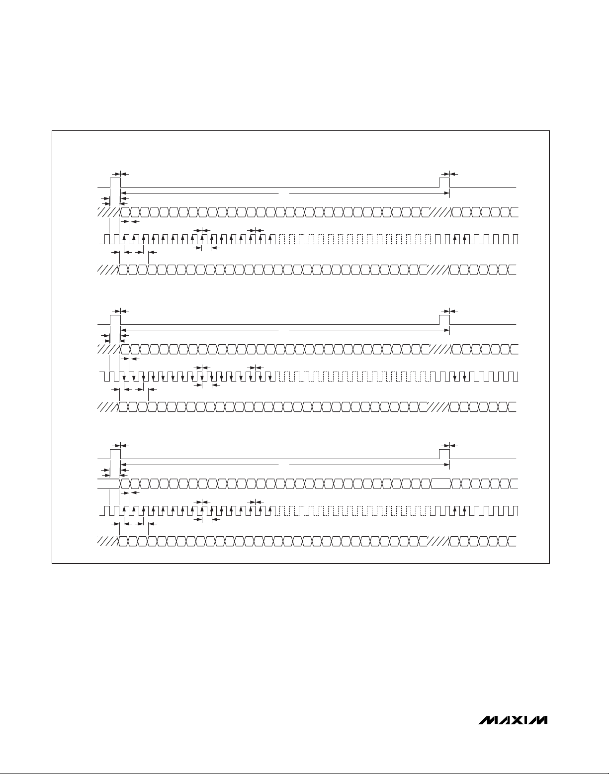
MAX9880A
Low-Power, High-Performance
Dual I2S Stereo Audio Codec
38 ______________________________________________________________________________________
Figure 3. Digital Audio Interface Voice Master Mode
VOICE (TDM/PCM) MASTER MODES:
TDM = 1, BCI = 0, HIZOFF = 0, SLOTDLY = 0, SLOT = 00, DLY = 0
7ns (typ)
LRCLK
200ns
SDOUT
BCLK
20ns (min) 0ns (min)
L15 L14 L13 L12 L11 L10 L9 L8 L7 L6 L5 L4 L3 L2
40ns (max)
0ns (min)
7ns (typ) 7ns (typ)
CONFIGURED BY BSEL
1/f
S
R14R15 R13 R12 R11 R10 R9 R8 R7 R6 R5 R4 R3 R2 R1 R0
L0
L1
7ns (typ)
SDIN
SDIN
LRCLK
SDOUT
BCLK
20ns (min) 0ns (min)
SDIN
LRCLK
SDOUT
BCLK
20ns (min) 0ns (min)
SDIN
L15 L14 L13 L12 L11 L10 L9 L8 L7 L6 L5 L4 L3 L2
TDM = 1, BCI = 1, HIZOFF = 0, SLOTDLY = 0, SLOT = 00
7ns (typ)
200ns
L15 L14 L13 L12 L11 L10 L9 L8 L7 L6 L5 L4 L3 L2
40ns (max)
0ns (min)
L15 L14 L13 L12 L11 L10 L9 L8 L7 L6 L5 L4 L3 L2
TDM = 1, BCI = 0, HIZOFF = 1, SLOTDLY = 0, SLOT = 00, DLY = 0
7ns (typ)
200ns
L15 L14 L13 L12 L11 L10 L9 L8 L7 L6 L5 L4 L3 L2
40ns (max)
0ns (min)
L15 L14 L13 L12 L11 L10 L9 L8 L7 L6 L5 L4 L3 L2
L0
L1
L0
L1
7ns (typ) 7ns (typ)
CONFIGURED BY BSEL
L0
L1
L0
L1
7ns (typ) 7ns (typ)
CONFIGURED BY BSEL
L0
L1
R14R15 R13 R12 R11 R10 R9 R8 R7 R6 R5 R4 R3 R2 R1 R0
1/f
S
R14R15 R13 R12 R11 R10 R9 R8 R7 R6 R5 R4 R3 R2 R1 R0
R14R15 R13 R12 R11 R10 R9 R8 R7 R6 R5 R4 R3 R2 R1 R0
1/f
S
R14R15 R13 R12 R11 R10 R9 R8 R7 R6 R5 R4 R3 R2 R1 R0
R14R15 R13 R12 R11 R10 R9 R8 R7 R6 R5 R4 R3 R2 R1 R0
7ns (typ)
7ns (typ)

MAX9880A
Low-Power, High-Performance
Dual I2S Stereo Audio Codec
______________________________________________________________________________________ 39
VOICE (TDM/PCM) SLAVE MODES:
Figure 4. Digital Audio Interface Voice Slave Mode
Table 8. Digital Mixers
Note: Register addresses listed are for I2C. To get the SPI address, add 0x200 with the following exception: Register 0xFF is not
accessible through SPI.
TDM = 1, BCI = 0, HIZOFF = 0, SLOTDLY = 0, SLOT = 00, DLY = 0
LRCLK
20ns
SDOUT
BCLK
20ns (min) 0ns (min)
SDIN
SDIN
LRCLK
SDOUT
BCLK
20ns (min) 0ns (min)
SDIN
SDIN
LRCLK
SDOUT
BCLK
20ns (min) 0ns (min)
SDIN
SDIN
L15 L14 L13 L12 L11 L10 L9 L8 L7 L6 L5 L4 L3 L2
40ns (max)
0ns (min)
L15 L14 L13 L12 L11 L10 L9 L8 L7 L6 L5 L4 L3 L2
TDM = 1, BCI = 1, HIZOFF = 0, SLOTDLY = 0, SLOT = 00, DLY = 0
20ns
40ns (max)
0ns (min)
L15 L14 L13 L12 L11 L10 L9 L8 L7 L6 L5 L4 L3 L2
TDM = 1, BCI = 0, HIZOFF = 1, SLOTDLY = 0, SLOT = 00, DLY = 0
20ns
L15 L14 L13 L12 L11 L10 L9 L8 L7 L6 L5 L4 L3 L2
40ns (max)
0ns (min)
L15 L14 L13 L12 L11 L10 L9 L8 L7 L6 L5 L4 L3 L2
1/f
L0
L1
30ns (min) 7ns (typ)
75ns (min)
L0
L1
30ns (min) 7ns (typ)
75ns (min)
L0
L1
L0
L1
30ns (min)
75ns (min)
L0
L1
S
R14R15 R13 R12 R11 R10 R9 R8 R7 R6 R5 R4 R3 R2 R1 R0
30ns (min)
R14R15 R13 R12 R11 R10 R9 R8 R7 R6 R5 R4 R3 R2 R1 R0
1/f
S
R14R15 R13 R12 R11 R10 R9 R8 R7 R6 R5 R4 R3 R2 R1 R0L15 L14 L13 L12 L11 L10 L9 L8 L7 L6 L5 L4 L3 L2 L1 L0
30ns (min)
R14R15 R13 R12 R11 R10 R9 R8 R7 R6 R5 R4 R3 R2 R1 R0
1/f
S
R14R15 R13 R12 R11 R10 R9 R8 R7 R6 R5 R4 R3 R2 R1 R0
30ns (min)
R14R15 R13 R12 R11 R10 R9 R8 R7 R6 R5 R4 R3 R2 R1 R0
0ns (min)
0ns (min)
0ns (min)
0ns (min)
0ns (min)
0ns (min)
REGISTER
REGISTER B7 B6 B5 B4 B3 B2 B1 B0
DIGITAL MIXERS
DAC-L/R Mixer MIXDAL MIXDAR 0x10
BITS FUNCTION
Digital Mixers (MIXDAL/MIXDAR). Selects and mi xe s the audio source(s) for the DAC s according to the
information below.
MIXDAL/MIXDAR SOURCE
MIXDAL/
MIXDAR
1xxx DAI1 left-channel data
x1xx DAI1 right-channel data
xx1x DAI2 left-channel data
xxx1 DAI2 right-channel data
ADDRESS
(SEE NOTE)

MAX9880A
Low-Power, High-Performance
Dual I2S Stereo Audio Codec
40 ______________________________________________________________________________________
Table 10. IIR Highpass Digital Filters
Digital Filtering
The MAX9880A incorporates both IIR (voice) and FIR
(audio) digital filters to accomodate a wide range of
audio sources. The IIR fiilters provide over 70dB of
stopband attenuation as well as selectable highpass filters. The FIR filters provide low power consumption and
are linear phase to maintain stereo imaging.
Table 9. Digital Filtering Register
Note: Register addresses listed are for I2C. To get the SPI address, add 0x200 with the following exception: Register 0xFF is not
accessible through SPI.
REGISTER
REGISTER B7 B6 B5 B4 B3 B2 B1 B0
DIGITAL FILTERING
Codec Filters MODE AVFLT DCB DVFLT 0x11
BITS FUNCTION
Digital Audio Filter Mode. Selects the fi ltering mode for the DAI1 DAC and ADC signal paths.
MODE
AVFLT
DCB
DVFLT
0 = IIR vo ice fi lters
1 = FIR audio filter s
ADC Digital Audio Filter. Configures the h ighpass filters for the DAI1 signal path.
MODE = 0
Select the desired digital fi lter response from Table 10. See the frequency response graphs in the Typical
Operating Characteristic s section for details on each filter.
MODE = 1
0x0 = DC-blocking filter disabled.
0x1 = DC-blocking filter enabled.
1 = DC-blocking fi lter for DAI2 enab led.
0 = DC-block ing fi lter for DAI2 disabled.
DAC Digital Audio Filter. Configures the h ighpass filters for the DAI1 signal path.
MODE = 0
Select the desired digital fi lter response from Table 10. See the frequency response graphs in the Typical
Operating Characteristic s section for details on each filter.
MODE = 1
0x0 = DC-blocking filter disabled.
0x1 = DC-blocking filter enabled.
ADDRESS
(SEE NOTE)
CODE FILTER TYPE
0x0 Disabled
0x1 Elliptica l 16 256Hz Yes
0x2 Butterworth 16 500Hz No
0x3 Elliptica l 8 256Hz Yes
0x4 Butterworth 8 500Hz No
0x5 Butterworth 8 to 24 fS/240 No
0x6 to 0x7 Reserved
VALID SAMPLE
RATE (kHz)
HIGHPASS CORNER FREQUENCY 217Hz NOTCH

MAX9880A
Low-Power, High-Performance
Dual I2S Stereo Audio Codec
______________________________________________________________________________________ 41
Table 11. SPDM Output Registers
Grayed boxes = Not used.
Note: Register addresses listed are for I
2
C. To get the SPI address, add 0x200 with the following exception: Register 0xFF is not
accessible through SPI.
The MAX9880A supports stereo PDM outputs. The PDM
signals consist of PDM data outputs (SPDMDATA) and a
clock output (SPDMCLK). The mixer at the input to the
PDM modulators allows a mix/mux of the audio digital data
stream from the digital audio ports SDINS1 and SDINS2.
Figure 5 shows the SPDM interface timing diagram.
Figure 5. SPDM Timing Diagram
REGISTER
REGISTER B7 B6 B5 B4 B3 B2 B1 B0
Conf iguration SPDMCLK SPDML SPDMR 0 0 0 0 0x12
Input MIXSPDML MIXSPDMR 0x13
SPDMCLK
t
DLY, DSD
SPDMDATA LEFT CH RIGHT CH LEFT CH RIGHT CH
t
DLY, DSD
ADDRESS
(SEE NOTE)
BITS FUNCTION
SPDM Clock Rate (SPDMCLK)
00 = SPDMCLK is set to PCLK/8.
SPDMCL K
SPDML/SPDM R
MIXSPDML/
MIXSPDMR
01 = SPDMCLK is set to PCLK6.
10 = SPDMCLK is set to PCLK/4.
11 = Reserved
0 = Dis ables SPDM data.
1 = Enables SPDM data.
SPDM Input Mixers. Selects and mixes the audio source(s) for the SPDM output according to following
information.
MIXS PDML/MIXSPDMR SOURCE
1xxx DAI1 left-channel data
x1xx DAI1 right-channel data
xx1x DAI2 left-channel data
xxx1 DAI2 right-channel data

MAX9880A
Low-Power, High-Performance
Dual I2S Stereo Audio Codec
42 ______________________________________________________________________________________
Digital Gain Control
The MAX9880A includes gain adjustment for the playback and record paths. Independent gain adjustment is
provided for the two record channels. Sidetone gain
adjustment is also provided to set the sidetone level relative to the playback level.
Table 12. Digital Gain Registers
Grayed boxes = Not used.
Note: Register addresses listed are for I
2
C. To get the SPI address, add 0x200 with the following exception: Register 0xFF is not
accessible through SPI.
REGISTER
REGISTER B7 B6 B5 B4 B3 B2 B1 B0
LEVEL CONTROL
Sidetone DSTS 0 DVST 0x15
Stereo DAC Leve l 0 SDACM 0 0 SDACA 0x16
Voice DAC Level 0 VDACM VDACG VDAC A 0x17
Left ADC Le ve l 0 0 AVLG AVL 0x18
Right ADC Level 0 0 AVRG AVR 0x19
BITS FUNCTION
Digital Sidetone Source Mixer
00 = No s idetone selected.
DSTS
DVST
01 = Left ADC
10 = R ight ADC
11 = Left and right ADC
Digital Sidetone Level Control. All gain settings are relative to the ADC input voltage.
Differential Headphone Output Mode
SETTING GAIN (dB) S ETTING GAIN (dB) SETTING GAIN (dB)
0x00 Off 0x0B -20 0x16 -42
0x01 0 0x0C -22 0x17 -44
0x02 -2 0x0D -24 0x18 -46
0x03 -4 0x0E -26 0x19 -48
0x04 -6 0x0F -28 0x1A -50
0x05 -8 0x10 -30 0x1B -52
0x06 -10 0x11 -32 0x1C -54
0x07 -12 0x12 -34 0x1D -56
0x08 -14 0x13 -36 0x1E -58
0x09 -16 0x14 -38 0x1F -60
0x0A -18 0x15 -40 — —
Capacitorless and Single-Ended Headphone Output Mode
SETTING GAIN (dB) S ETTING GAIN (dB) SETTING GAIN (dB)
0x00 Off 0x0B -25 0x16 -47
0x01 -5 0x0C -27 0x17 -49
0x02 -7 0x0D -29 0x18 -51
0x03 -9 0x0E -31 0x19 -53
0x04 -11 0x0F -33 0x1A -55
0x05 -13 0x10 -35 0x1B -57
0x06 -15 0x11 -37 0x1C -59
0x07 -17 0x12 -39 0x1D -61
0x08 -19 0x13 -41 0x1E -63
0x09 -21 0x14 -43 0x1F -65
0x0A -23 0x15 -45 — —
ADDRESS
(SEE NOTE)

MAX9880A
Low-Power, High-Performance
Dual I2S Stereo Audio Codec
______________________________________________________________________________________ 43
Table 12. Digital Gain Registers (continued)
BITS FUNCTION
SDACM/
VDACM
VDACG
VDACA/SDACA
AVLG/AV RG
AVL/AV R
DAC Mute Enable
0 = No mute
1 = Mute
DAC Gain
00 = 0dB
01 = +6dB
10 = +12dB
11 = +18dB
Note: VDACG is only used when MODE = 0. If MODE = 1, then the DAC gain is always 0dB.
DAC Level Control. VDACA/SDACA works in all modes.
SETTING GAIN (dB) S ETTING GAIN (dB)
0x0 0 0x8 -8
0x1 -1 0x9 -9
0x2 -2 0xA -10
0x3 -3 0xB -11
0x4 -4 0xC -12
0x5 -5 0xD -13
0x6 -6 0xE -14
0x7 -7 0xF -15
ADC Gain Control. Applies the specified gain to the digital ADC paths according to the following
information.
SETTING GAIN (dB)
0x0 0
0x1 +6
0x2 +12
0x3 +18
ADC Left/Right Level Control
SETTING GAIN (dB) S ETTING GAIN (dB)
0x0 +3 0x8 -5
0x1 +2 0x9 -6
0x2 +1 0xA -7
0x3 0 0xB -8
0x4 -1 0xC -9
0x5 -2 0xD -10
0x6 -3 0xE -11
0x7 -4 0xF -12

MAX9880A
Low-Power, High-Performance
Dual I2S Stereo Audio Codec
44 ______________________________________________________________________________________
Line Inputs
The MAX9880A include one pair of single-ended line
inputs. When enabled the line inputs connect directly to
the headphone amplifier and line outputs and can be
optionally connected to the ADC for recording.
Playback Volume
The MAX9880A incorporates volume and mute control to
allow level control for the playback audio path. Program
registers 0x1C and 0x1D to set the desired volume.
Line Output Level
The MAX9880A incorporates gain and mute control to
allow level control for the line outputs.
Table 13. Line Input Registers
Table 14. Playback Volume Registers
Grayed boxes = Not used.
Note: Register addresses listed are for I
2
C. To get the SPI address, add 0x200 with the following exception: Register 0xFF is not
accessible through SPI.
Grayed boxes = Not used.
Note: Register addresses listed are for I
2
C. To get the SPI address, add 0x200 with the following exception: Register 0xFF is not
accessible through SPI.
REGISTER B7 B6 B5 B4 B3 B2 B1 B0
Left-Line Input Leve l 0 LILM 0 0 LIGL 0x1A
Right-Line Input Level 0 LIRM 0 0 LIGR 0x1 B
BITS FUNCTION
Line Input Left/Right Playback Mute
LILM/LIRM
LIGL/LIGR
0 = Line input is connected to the headphone amplifiers.
1 = Line input is disconnected from the headphone amplifiers.
Line Input Left/Right Gain
SETTING GAIN (dB) SETTING GAIN (dB)
0x0 +24 0x8 +8
0x1 +22 0x9 +6
0x2 +20 0xA +4
0x3 +18 0xB +2
0x4 +16 0xC 0
0x5 +14 0xD -2
0x6 +12 0xE -4
0x7 +10 0xF -6
REGISTER
ADDRESS
(SEE NOTE)
REGISTER
REGISTER B7 B6 B5 B4 B3 B2 B1 B0
Left Volume Control 0 VOLLM VOLL 0x1C
Right Volume Control 0 VOLRM VOLR 0x1D
BITS FUNCTION
Left/Right Playback Mute. VOLLM and VOLRM mute both the DAC and line input audio signals.
VOLLM/
VOL R M
0 = Audio playback is unmuted.
1 = Audio playback is muted.
Note: VSEN has no effect on the mute function. When VOLLM or VOLRM i s set, the output i s muted
immediately (ZDEN = 1) or at the next zero-crossing (ZDEN = 0).
ADDRESS
(SEE NOTE)

MAX9880A
Low-Power, High-Performance
Dual I2S Stereo Audio Codec
______________________________________________________________________________________ 45
Table 14. Playback Volume Registers (continued)
Table 15. Output Line-Level Registers
Grayed boxes = Not used.
Note: Register addresses listed are for I
2
C. To get the SPI address, add 0x200 with the following exception: Register 0xFF is not
accessible through SPI.
BITS FUNCTION
Left/Right Playback Volume. VOLL and VOLR control the playback volume for both the DAC and line input
audio s ignal s.
SETTING GAIN (dB) S ETTING GAIN (dB) SETTING GAIN (dB)
0x00 +9 0x0E -2 0x1C -39
0x01 +8.5 0x0F -3 0x1D -43
0x02 +8 0x10 -5 0x1E -47
0x03 +7.5 0x11 -7 0x1F -51
0x04 +7 0x12 -9 0x20 -55
0x05 +6.5 0x13 -11 0x21 -59
VOLL/VOLR
0x06 +6 0x14 -13 0x22 -63
0x07 +5 0x15 -15 0x23 -67
0x08 +4 0x16 -17 0x24 -71
0x09 +3 0x17 -19 0x25 -75
0x0A +2 0x18 -23 0x26 -79
0x0B +1 0x19 -27 0x27 -81
0x0C 0 0x1A -31
0x0D -1 0x1B -35
Note: Gain settings apply when the headphone amplif ier i s configured in differential mode. In the s ingleended and capacitorle ss modes, the actual gain is 5dB lower. Assum ing LOGL/LOGR = 0dB, line output
gain is 6dB lower.
0x28 to 0x3F MUTE
REGISTER
REGISTER B7 B6 B5 B4 B3 B2 B1 B0
Left-Line Output Level 0 LOLM
Right-Line Output Le ve l 0 LORM 0 0 LOGR 0x1F
0
0 LOGL 0x1E
ADDRESS
(SEE NOTE)
BITS FUNCTION
Left/Right Line Output Mute. LOLM and LORM mute both the DAC and line input audio signals.
0 = Line output is unmuted.
LOLM/LORM
LOGL/LOGR
1 = Line output is muted.
Note: VSEN has no effect on the mute function. When LOLM or LORM is set the output is muted immediately
(ZDEN = 1) or at the ne xt zero-crossing (ZDEN = 0).
Left/Right Line Output Gain. LOGL and LOGR set the l ine output gain according to the fol low ing information.
SETTING GAIN (dB) SETTING GAIN (dB)
0x00 0 0x08 -16
0x01 -2 0x09 -18
0x02 -4 0x0A -20
0x03 -6 0x0B -22
0x04 -8 0x0C -24
0x05 -10 0x0D -26
0x06 -12 0x0E -28
0x07 -14 0x0F -30

MAX9880A
Low-Power, High-Performance
Dual I2S Stereo Audio Codec
46 ______________________________________________________________________________________
Microphone Inputs
Two differential microphone inputs and a low noise 1.5V
microphone bias for powering the microphones are
provided by the MAX9880A. In typical applications, the
left microphone records a voice signal and the right
microphone records a background noise signal. In
applications that require only one microphone, use the
left microphone input and disable the right ADC. The
microphone signals are amplified by two stages of gain
and then routed to the ADCs. The first stage offers
selectable 0dB, 20dB, or 30dB settings. The second
stage is a programmable gain amplifier (PGA)
adjustable from 0dB to 20dB in 1dB steps. Zero-crossing detection is included on the PGA to minimize zipper
noise while making gain changes. See Figure 6 for a
detailed diagram of the microphone input structure.
Table 16. Microphone Input Registers
Figure 6. Microphone Input Block Diagram
Grayed boxes = Not used.
Note: Register addresses listed are for I
2
C. To get the SPI address, add 0x200 with the following exception: Register 0xFF is not
accessible through SPI.
MICBIAS
1.5V
MICLP
MICLN
MICRP
MICRN
MAX9880A
0/20/30dB
V
REG
PREAMP
0/20/30dB
PREAMP
PGA
-
V
0dB TO +20dB
REG
PGA
ADC
L
ADC
R
0dB TO +20dB
REGISTER
REGISTER B7 B6 B5 B4 B3 B2 B1 B0
Left Microphone Gain 0 PALEN PGAML 0x20
Right Microphone Gain 0 PAREN PGAMR 0x21
BITS FUNCTION
Left/Right Microphone Preamplifier Gain. Enables the microphone circuitry and sets the preamplifier gain.
PALEN/
PAREN
00 = Disabled
01 = 0dB
10 = +20dB
11 = +30dB
ADDRESS
(SEE NOTE)

MAX9880A
Low-Power, High-Performance
Dual I2S Stereo Audio Codec
______________________________________________________________________________________ 47
Table 16. Microphone Input Registers (continued)
ADC
The MAX9880A includes two 18-bit ADCs. The first
ADC is used to record left-channel microphone and
line-input audio signals. The second ADC can be used
to record right-channel microphone and line-input signals or it can be configured to accurately measure DC
voltages.
When measuring DC voltages both the left and right ADC
must be enabled by setting ADLEN and ADREN in register 0x26. The input to the second ADC is JACKSNS/
AUX and the output is reported in AUX (registers 0x02
and 0x03). Since the audio ADC is used to perform the
measurement, the digital audio interface must be properly configured. If the left ADC is being used to convert
audio, then the DC measurement is performed at the
same sample rate. When not using the left ADC, configure the digital interface for a 48kHz sample rate to
ensure the fastest possible settling time.
To ensure accurate results, the MAX9880A includes
two calibration routines. Calibrate the ADC each time
the MAX9880A is powered on. Calibration settings are
not lost if the MAX9880A is placed in shutdown. When
making a measurement, set AUXCAP to 1 to prevent
AUX from changing while reading the registers.
Setup Procedure
1) Ensure a valid MCLK signal is provided and configure PSCLK appropriately.
2) Choose a clocking mode. The following options are
possible:
a. Slave mode with LRCLK and BCLK signals
provided. The measurement sample rate is
determined by the external clocks.
b. Slave mode with no LRCLK and BCLK signals
provided. Configure the device for normal clock
mode using the NI ratio. Select fS= 48kHz to
allow for the fastest settling times.
c. Master mode with audio. Configure the device
in normal mode using the NI ratio or exact integer mode using FREQ1 as required by the audio
signal.
d. Master mode without audio. Configure the
device in normal mode using the NI ratio. Select
fS= 48kHz to allow for the fastest settling times.
3) Ensure jack sense is disabled.
4) Enable the left and right ADC; take the MAX9880A
out of shutdown.
BITS FUNCTION
Left/Right Microphone Programmable Gain Amplifier
SETTING GAIN (dB) SETTING GAIN (dB)
0x00 +20 0x0B +9
0x01 +19 0x0C +8
0x02 +18 0x0D +7
PGAML/
PGAMR
0x03 +17 0x0E +6
0x04 +16 0x0F +5
0x05 +15 0x10 +4
0x06 +14 0x11 +3
0x07 +13 0x12 +2
0x08 +12 0x13 +1
0x09 +11 0x14 to 0x1F 0
0x0A +10

MAX9880A
Low-Power, High-Performance
Dual I2S Stereo Audio Codec
48 ______________________________________________________________________________________
Offset Calibration Procedure
Perform before the first DC measurement is taken after
applying power to the MAX9880A.
1) Enable the AUX input (AUXEN = 1).
2) Enable the offset calibration (AUXCAL = 1).
3) Wait the appropriate time (see Table 17).
4) Complete calibration (AUXCAL = 0).
Gain Calibration Procedure
Perform the first time a DC measurement is taken after
applying power to the MAX9880A or if the temperature
changes significantly.
1) Enable the AUX input (AUXEN = 1).
2) Start gain calibration (AUXGAIN = 1).
3) Wait the appropriate time (see Table 17).
4) Freeze the measurement results (AUXCAP = 1).
5) Read AUX and store the value in memory to correct
all future measurements (k = AUX[15:0], k is typically 19,500).
6) Complete calibration (AUXGAIN = AUXCAP = 0).
DC Measurement Procedure
Perform after offset and gain calibration are complete.
1) Enable the AUX input (AUXEN = 1).
2) Wait the appropriate time (see Table 17).
3) Freeze the measurement results (AUXCAP = 1).
4) Read AUX and correct with the gain calibration value
5) Complete measurement (AUXCAP = 0).
Complete DC Measurement Example
f
MCLK
= 13MHz, slave mode, BCLK, and LRCLK are
not externally supplied.
1) Configure the digital audio interface for fs= 48kHz
(PSCLK = 01, FREQ1 = 0x0, PLL = 0, NI = 0x5ABE,
MAS = 0).
2) Disable jack sense (JDETEN = 0).
3) Enable the left and right ADC; take the MAX9880A
out of shutdown (ADLEN = ADREN = SHDN = 1).
4) Calibrate the offset:
a. Enable the AUX input (AUXEN = 1).
b. Enable the offset calibration (AUXCAL = 1).
c. Wait 40ms.
d. Complete calibration (AUXCAL = 0).
5) Calibrate the gain:
a. Start gain calibration (AUXGAIN = 1).
b. Wait 40ms.
c. Freeze the measurement results (AUXCAP = 1).
d. Read AUX and store the value in memory to cor-
rect all future measurements (k = AUX[15:0]).
e. Complete calibration (AUXGAIN = AUXCAP =
AUXEN = 0).
6) Measure the voltage on JACKSNS/AUX.
a. Enable the AUX input (AUXEN = 1).
b. Wait 40ms.
c. Freeze the measurement results (AUXCAP = 1).
d. Read AUX and correct with the gain calibration
value.
e. Complete measurement (AUXCAP = 0).
7) DC measurement is complete.
Table 17. AUX ADC Wait Times
⎛
V
=
AUX
⎜
⎝
0 738
AUX
15 0
[:]
⎛
.
⎜
⎝
k
⎞
⎞
.
⎟
⎟
⎠
⎠
LRCLK (kHz) WAIT TIME (ms)
48 40
44.1 44
32 60
24 80
22.05 90
16 120
12 160
11.025 175
8 240

MAX9880A
Low-Power, High-Performance
Dual I2S Stereo Audio Codec
______________________________________________________________________________________ 49
Table 18. ADC Input Register
Note: Register addresses listed are for I2C. To get the SPI address, add 0x200 with the following exception: Register 0xFF is not
accessible through SPI.
REGISTER
REGISTER B7 B6 B5 B4 B3 B2 B1 B0
Input MXINL MXINR AUXCAP AUXGAIN AUXCAL AUXEN 0x22
BITS FUNCTION
Left/Right ADC Audio Input Mixer
00 = No input selected
01 = Left/right analog microphone
MXINL/MXINR
AUXCAP
AUXGAIN
AUXCAL
AUXEN
10 = Left/right line input
11 = Left/right analog microphone + line input
Note: If the right line input is disabled, then the left line input is connected to both mixers. Enabling the left
and right digital m icrophones disable s the left and right audio m ixer, respectively. See the DIGMICL/
DIGMICR bit description for more detai ls.
Auxiliary Input Capture
0 = Update AUX with the voltage at JACKSNS/AUX.
1 = Hold AUX for reading.
Auxilia ry Input Gain Calibration
0 = Normal operation
1 = The input buffer is disconnected from JACKSNS/AUX and connected to an internal voltage reference.
While in this mode, read the AUX register and store the va lue. Use the stored value a s a gain
cal ibration factor, k, on subsequent readings. AUXCAL must remain set for time indicated in Table 17 to
guarantee an accurate offset calibration.
Auxiliary Input Offset Calibration
0 = Normal operation
1 = JACKSNS/AUX is disconnected from the input and the ADC automatically calibrates out any internal
offsets. AUXCAL must remain set for time indicated in Table 17 to guarantee an accurate offset
cal ibration.
Auxiliary Input Enable
0 = Use JACKSNS/AUX for jack detection.
1 = Use J ACKSNS/AUX for DC measurements.
Note: Set MXINR = 00, ADLEN = 1, and ADREN = 1 when AUXEN = 1.
ADDRESS
(SEE NOTE)

MAX9880A
Low-Power, High-Performance
Dual I2S Stereo Audio Codec
50 ______________________________________________________________________________________
Digital Microphone Input
The MAX9880A can accept audio from up to two digital microphones. When using digital microphones, the
left analog microphone input is retasked as a digital
microphone input. The right analog microphone input is
still available to allow a combination of analog and digital microphones to be used. Figure 7 shows the digital
microphone interface timing diagram.
Figure 7. Digital Microphone Timing Diagram
Table 19. Digital Microphone Input Register
Grayed boxes = Not used.
Note: Register addresses listed are for I
2
C. To get the SPI address, add 0x200 with the following exception: Register 0xFF is not
accessible through SPI.
DIGMICCLK
DIGMICDATA
t
HD, MIC
LEFT RIGHT LEFT RIGHT
t
SU, MIC
1/f
MICCLK
t
HD, MIC
t
SU, MIC
REGISTER
REGISTER B7 B6 B5 B4 B3 B2 B1 B0
Microphone MICCLK DIGMICL DIGMICR 0 0 0 MBIAS 0x23
ADDRESS
(SEE NOTE)
BITS FUNCTION
Digital Microphone Clock
00 = PCLK/8
MICCLK
DIGMICL/
DIGMICR
MBIAS
01 = PCLK/6
10 = 64f
11 = Reserved
Digital Left/Right Mic rophone Enable
Note: The left analog microphone input is ne ver ava ilable when DIGMICL or DIGMICR = 1.
Mic rophone Bias Output Voltage
Set MBIAS = 0 for nominal output of 1.52V (V
Set MBIAS = 1 for nominal output of 2.2V (V
(high jitter clock)
S
DIGMICL DIGMICR LEFT ADC INPUT RIGHT ADC INPUT
0 0 ADC input mixer ADC input mixer
0 1
1 0 Left digital microphone ADC input mixer
1 1 Left digital microphone Right digital m icrophone
MICVDD
MICVDD
Line input (left analog
microphone unavailable)
= 1.8V)
= 3V)
Right digital microphone

Jack Configuration Change Flag (JDET)
1 = Jack configuration has changed.
0 = No change in jack configuration.
JDET reports changes in JKSNS[1:0]. Changes to
JKSNS[1:0] are debounced before setting JDET. The
debounce period is programmable using the JDEB bits.
Jack status register 0x01 is a read-only register that reports
the status of the jack-detect circuitry when enabled.
Jack Sense (JKSNS)
JKSNS[1:0] reports the status of the JACKSNS pin
when JDETEN = 1. JKSNS[1:0] should be interpreted
according to Table 21.
Jack-Detect Interrupt Enable (IJDET)
Hardware interrupts are reported on the open-drain IRQ
pin. When an interrupt occurs, IRQ remains low until the
interrupt is serviced by reading the status register 0x00.
If a flag is set, it is reported as a hardware interrupt only
if the corresponding interrupt enable is set. Each bit
enables interrupts for the status flag in the respective
bit location in register 0x00. So IJDET must be set to
enable interrupts for jack detect.
Jack-Detect Enable (JDETEN)
Enables the jack-detect circuitry.
Jack-Sense Weak Pullup (JDWK)
Enables a weak internal pullup current for reduced
power loss when the chip is in shutdown or the
MICBIAS is disabled.
JDWK = 0 enables a 2.2kΩ pullup to obtain full jackdetect operation. This mode can be used to detect
insertion and removal of a plug as well as distinguish
between headphone and headset accessories.
JDWK = 1 enables a 4µA pullup current source when
SHDN = 0 or MICBIAS disabled. In this power-saving
configuration, the circuit can detect insertion and
removal of a plug but cannot distinguish between headphone and headset accessories.
The recommended usage follows: Set JDWK = 0 (or set
any bit in the microphone preamplifier gain registers
PALEN[1:0] or PAREN[1:0]). This enables the 2.2kΩ
pullup. Once the jack has been inserted and the type of
accessory determined, set JDWK = 1 to save power.
Once the plug is removed, set JDWK = 0.
MAX9880A
Low-Power, High-Performance
Dual I2S Stereo Audio Codec
______________________________________________________________________________________ 51
Mode Configuration
The MAX9880A includes circuitry to minimize click-andpop during volume changes, detect headsets, and configure the headphone amplifier mode. Both volume
slewing and zero-crossing detection are included to
ensure click-and-pop free volume transitions.
Headset Detection Overview
The MAX9880A contains headset detect circuitry that is
capable of detecting the insertion or removal of a plug
and providing information to assist the system controller
in determining the configuration of an inserted plug. If
programmed to do so, upon insertion or removal of a
plug, the IRQ output is asserted (pulled low).
Table 20 shows the registers associated with the jack
detect function in MAX9880A.
Table 21. Jack Sense (JKSNS)
Table 20. Jack-Detect Registers
Grayed boxes = Not used.
REGISTER B7 B6 B5 B4 B3 B2 B1 B0
Status CLD SLD ULK — * * JDET — 0x00 — R
Jac k Status JKSNS[1:0] — — — — — — 0x01 — R
Interrupt Enable ICLD ISLD IULK 0 0* 0* IJDET 0 0x04 0x00 R/W
Jack Detect JDETEN 0 JDWK 0 0 0 JDEB 0x25 0x00 R/W
REGISTER
ADDRESS
POR STATE R/ W
JKSNS[1:0] DESCRIPTION
00 JACKSNS i s below V
01 JACKSNS i s between V
10 Inval id.
11 J ACKSNS is above V
TH2
TH1
(low).
and V
TH1
(high).
TH2
(mid).

MAX9880A
Low-Power, High-Performance
Dual I
2
S Stereo Audio Codec
52 ______________________________________________________________________________________
Figure 8. Typical Configuration for Headset Detection
Debounce (JDEB)
Configures the JDET debounce time for changes to
JKSNS[1:0] according to Table 22.
For jack plug insertion/removal, the sequence of events
is as follows:
Jack insertion: No jack is present. The MAX9880A has
a power supply and is in low-power sleep mode
(LOUTP/ROUTP are high impedance). When the
JDETEN I
2
C bit is set, the JACKSNS pin has weak
pullups to MICVDD. When a jack is subsequently inserted, JACKSNS should change state (indicated by I
2
C
bits JKSNS[1:0]), and this causes the IRQ pin to be
pulled low, which can trigger a system wakeup.
Jack present: After an interrupt has been sent to the
system controller, the I
2
C must indicate unambiguously
that a jack is present when the I
2
C registers are read.
This is done with the JDET I
2
C bit, which goes high
when there is a change of state of the JKSNS[1:0] bits.
The MAX9880A jack-detect system monitors the
JACKSNS pin and reports the voltage level as high
(> 95% x MICBIAS), mid, or low (< 10% x MICBIAS).
When connected to the microphone pin of the headset
jack, this window comparator allows detection of:
• No headset (high)
• Cellular headset with microphone (high → mid)
• Stereo headset without microphone (high → low)
• Cellular headset button press (mid → low → mid)
• Headset removal (low or mid → high)
Jack removal: A jack is present. All output poles
(headphones/line outs) are assumed driven by a low
impedance amplifier. All input poles (microphones) are
assumed to be biased with a voltage above ground but
below 95% of the MICBIAS voltage. For the MAX9880A
to sense when a jack is removed, the JACKSNS pin
must be connected to the jack in such a way as to
ensure either the JACKSNS pin gets pulled above 95%
of MICBIAS (as would happen if JACKSNS is hooked to
a microphone pole) or it changes state from low to high
or vice versa (as would happen if JACKSNS is hooked
to a ground pole which goes high impedance when the
jack is removed, or is hooked to a regular jack insertion
tab that shorts to ground when the jack is removed).
Subsequently, IRQ is pulled low.
Jack absent: After an interrupt has been sent to the
system controller, the I
2
C must indicate unambiguously
that a jack is not present when the I
2
C registers are
read. This is indicated by reading the status of the
JKSNS[1:0] I
2
C read bits.
Table 22. Debounce Time
MIC GND HPR HPL
LOUTP
MICBIAS
JACKSNS/AUX
ROUTP
MICLP
JDEB DEBOUNCE (ms)
00 25
01 50
10 100
11 200

MAX9880A
Low-Power, High-Performance
Dual I2S Stereo Audio Codec
______________________________________________________________________________________ 53
Table 23. Headset Detect Configuration
Note: JDETEN = 1; MICBIAS enable; any bit of PALEN/PAREN set.
SHDN MICBIAS JDWK
0 — 0 None Headset 11 01 Yes No
0 — 0 None Headphone 11 00 Yes No
0 — 0 Head set None 01 11 Yes No
0 — 0 Headphone None 00 11 Yes No
0 — 1 None Headset 11 00 Yes No
0 — 1 None Headphone 11 00 Yes No
0 — 1 Head set None 00 11 Yes No
0 — 1 Headphone None 00 11 Yes No
1 0 0 None Headset 11 01 Yes No
1 0 0 None Headphone 11 00 Yes No
1 0 0 Headset None 01 11 Yes No
1 0 0 Headphone None 00 11 Yes No
1 0 1 None Headset 11 00 Yes No
1 0 1 None Headphone 11 00 Yes No
1 0 1 Headset None 00 11 Yes No
1 0 1 Headphone None 00 11 Yes No
1 1 — None Headset 11 01 Yes No
1 1 — None Headphone 11 00 Yes No
1 1 — Headset None 01 11 Yes No
1 1 — Headphone None 00 11 Yes No
JACK ACTION JKSNS IRQ TOGGLE S?
FROM TO FROM TO IJDET = 1 IJDET = 0

MAX9880A
Low-Power, High-Performance
Dual I2S Stereo Audio Codec
54 ______________________________________________________________________________________
Figure 9. Headphone Amplifier Modes
Table 24. Mode Configuration Register
Headphone Modes
The MAX9880A’s headphone amplifier supports differential, single-ended, and capacitorless output modes, as
shown in Figure 9. In each mode, the amplifier can be
configured for stereo or mono operation. The single-
ended mode optionally includes click-and-pop reduction to eliminate the click-and-pop that would normally
be caused by the output coupling capacitor. When
click-and-pop reduction is not required leave LOUTN
and ROUTN unconnected.
Grayed boxes = Not used.
Note: Register addresses listed are for I
2
C. To get the SPI address, add 0x200 with the following exception: Register 0xFF is not
accessible through SPI.
DIFFERENTIAL
LOUTP
LOUTN
ROUTP
ROUTN
OPTIONAL COMPONENTS REQUIRED FOR CLICK-AND-POP SUPPRESSION ONLY.
CAPACITORLESS
LOUTP
LOUTN
ROUTP
ROUTN
SINGLE-ENDED
220µF
LOUTP
LOUTN
1µF
220µF
ROUTP
ROUTN
1µF
REGISTER
REGISTER B7 B6 B5 B4 B3 B2 B1 B0
Mode DSLEW VSEN ZDEN 0 0 HPMODE 0x24
Jack Detect JDETEN 0 JDWK 0 0 0 JDEB 0x25
ADDRESS
(SEE NOTE)
BITS FUNCTION
Digital Volume Slew Speed
DSLEW
VSEN
ZDEN
0 = Digita l volume changes are slewed over 10ms.
1 = Digita l volume changes are slewed over 80ms.
Volume Change Smoothing
0 = Volume changes slew through all intermediate values.
1 = Volume changes occur in one step.
Line Input Zero-Crossing Detection
0 = Line input volume changes occur at zero crossings in the audio waveform or after 62ms if no zero
crossing occurs.
1 = Line input volume changes occur immediately.

MAX9880A
Low-Power, High-Performance
Dual I2S Stereo Audio Codec
______________________________________________________________________________________ 55
Table 24. Mode Configuration Register (continued)
Power Management
The MAX9880A includes complete power management
control to minimize power usage. The DAC and both
ADCs can be independently enabled so that only the
required circuitry is active.
Revision Code
The MAX9880A includes a revision code to allow easy
identification of the device revision. Revision code at
register address 0xFF is not accessible through the SPI
interface and so the revision code is accessible
through SPI at an additional address of 0x214. The current revision code is 0x42.
BITS FUNCTION
Headphone Amplifier Mode
HPMODE MODE
000 Stereo differential
001 Mono (left) different ia l
010 Stereo capacitorles s
HPMODE
JDETEN
JDWK
JDEB
Note: In mono operation, the right amp lifier is disabled.
Jack-Detection Enable
SHDN = 0: Sleep Mode. Enables pullups on JACKSNS/AUX to detect jac k insertion.
SHDN = 1: Normal Mode. Enables the comparator circuitry on JACKSNS/AUX to detect voltage changes.
Note: AUXEN must be set to 0 for jack detection to function.
Jack-Sense Weak Pullup. Enable s an internal pullup. Set JDWK = 1 to enable an internal 4µA current
source. Set JDWK = 0 for external pullup.
Jac k Detect Debounce. Configures the JDET debounce time for changes to JKSNS[1:0] according to
information below.
011 Mono (left) capacitorles s
100 Stereo single-ended (clickless)
101 Mono ( left) s ingle-ended (clickless)
110 Stereo single-ended (fast turn-on)
111 Mono (left) single-ended (fast turn-on)
JDEB DEBOUNCE TIME (ms)
00 25
01 50
10 100
11 200

MAX9880A
Low-Power, High-Performance
Dual I2S Stereo Audio Codec
56 ______________________________________________________________________________________
Table 25. Power Management Register
Table 26. Revision Code Register
Grayed boxes = Not used.
Note: Register addresses listed are for I
2
C. To get the SPI address, add 0x200 with the following exception: Register 0xFF is not
accessible through SPI.
Note: Register addresses listed are for I
2
C. To get the SPI address, add 0x200 with the following exception: Register 0xFF is not
accessible through SPI.
REGISTER
REGISTER B7 B6 B5 B4 B3 B2 B1 B0
Enable LNLEN LNREN LOLEN LOREN DALEN DAREN ADLEN ADREN 0x26
System Shutdown SHDN 0 0 0 XTEN XTOSC 0 0 0x27
BITS FUNCTION
Left-Line Input Enable. Enable s the left-line input preamp and automat ical ly enables the left and right
LNLEN
LNREN
LOLEN Left-Line Output Enable. Enables the left-line output.
LOREN Right-Line Output Enable. Enables the right-line output.
DALEN
DAREN Right DAC Enable. Enable s the right DAC. Right DAC operation requires DA LEN = 1.
ADLEN Left ADC Enable.
ADREN
SHDN Shutdown. Places the device in low power shutdown mode.
XTEN
XTOSC
headphone amplifiers. If LNREN = 0, the left-l ine input signal is also routed to the right ADC input mixer and
right headphone amplifier.
Note: Control of the right headphone ampl ifier can be overridden by HPMODE.
Right-Line Input Enable. Enables the right-line input preamp and automatica lly enables the right headphone
amplifiers.
Note: Control of the right headphone ampl ifier can be overridden by HPMODE.
Left DAC Enable. Enables the left DAC and automatica l ly enables the left and right headphone amplifiers. If
DAREN = 0, the left DAC signal i s a lso routed to the right headphone amplif ier.
Note: Control of the right headphone ampl ifier can be overridden by HPMODE.
Right ADC Enable. Enabling the right ADC must be done in the same I
ADC. The right ADC can be enabled while the left ADC is running if u sed for DC measurements. SHDN mu st
be toggled to disable the right ADC in th is ca se. Right ADC operation requires ADLEN = 1.
Crystal Clock Enable
1 = Output of crystal osc illator and buffer routed to the cloc k presca ler. MCLK input disabled.
0 = MCLK input routed to the clock prescaler. Crystal oscillator and buffer disabled.
Crystal Clock Source
1 = Disables the internal crystal oscillator. Provide an external clock on X1.
0 = Enables the internal crystal oscillator. Attach a crystal between X1 and X2. XTOSC i s ignored if XTEN = 0.
2
C write operation that enables the left
ADDRESS
(SEE NOTE)
REGISTER
REGISTER B7 B6 B5 B4 B3 B2 B1 B0
Revision ID REV 0x14
Revision ID REV 0xFF
ADDRESS
(SEE NOTE)
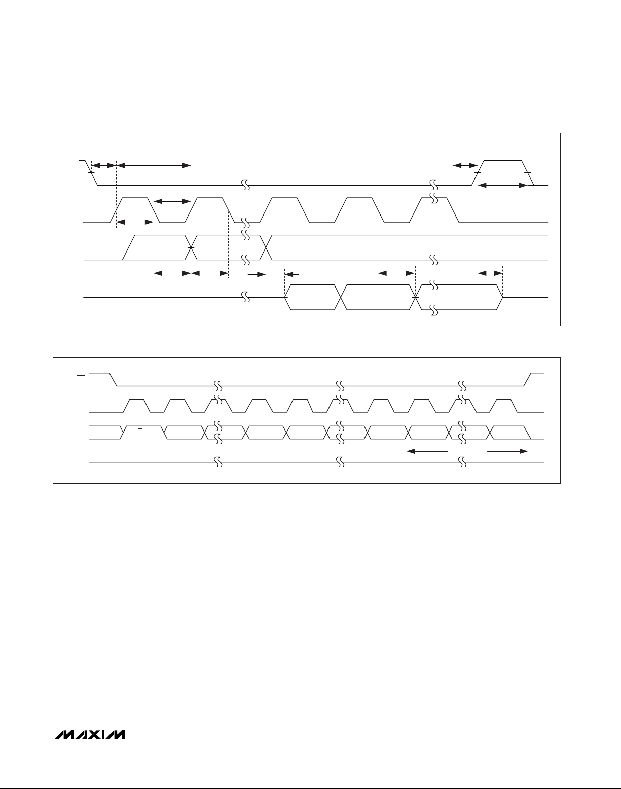
MAX9880A
Low-Power, High-Performance
Dual I
2
S Stereo Audio Codec
______________________________________________________________________________________ 57
Figure 10. SPI Interface Timing Diagram
Figure 11. Writing 1 Byte of Data to the MAX9880A
Serial Peripheral Interface (SPI)
Chip Select (CS)
The MAX9880A SPI interface is active only when CS is
low. When CS is high, the MAX9880A configures the
DOUT output for high impedance and resets the internal SPI logic. If CS goes high in the middle of an SPI
transfer, all the data is discarded. When CS is low,
unless the register address is correctly decoded by the
MAX9880A, the DOUT output is high impedance.
Serial Clock (SCLK)
The SPI master provides the SCLK signal to clock the
SPI interface. SCLK has an upper frequency limit of
25MHz. The MAX9880A samples the DIN input data on
the falling edge of SCLK and changes the output data
on the rising edge of SCLK. The MAX9880A ignores
SCLK transitions when CS is high.
Serial-Data In (DIN) and Serial-Data Out (DOUT)
The SPI frame is organized into 24 bits. The first 16 bits
consist of the R/W enable bit, followed by the 10 register address bits and 5 unused bits. The next 8 bits are
data bits, sent most significant bit first.
For an SPI write transfer, write a 1 to the R/W bit, followed by the 10 register address bits, 5 unused bits,
then the 8 data bits.
Figure 11 illustrates the proper frame format for writing
one byte of data to the MAX9880A. Additional 24-bit
frames can be sent while CS remains low. The DOUT
output is high impedance during a write operation.
For an SPI read transfer, write a zero to the R/W bit, followed by the 10 register address bits and 5 unused
bits. Any data sent after the register address bits are
ignored. The internal contents of the register being read
t
CSS
CS
SCLK
DIN
DOUT
CS
SCLK
DIN
t
CP
t
CL
t
CH
t
DH
R/W ADDR9 ADDR0 UNUSED4 UNUSED0 D7 D0
t
CSH
t
CSW
t
DS
t
DEN
t
DO
t
DZ
DOUT
HIGH-Z
1 DATA BYTE

MAX9880A
Low-Power, High-Performance
Dual I2S Stereo Audio Codec
58 ______________________________________________________________________________________
Figure 12. Reading 1 Byte of Data from the MAX9880A
Figure 13. Reading n Bytes of Data from the MAX9880A
SMBus is a trademark of Intel Corp.
do not change until the transfer is complete. The DOUT
output is high impedance when writing the register
address bits. If the correct register address is decoded, DOUT is driven low at the first rising clock edge
after the first unused bit.
Figure 12 illustrates the proper frame format for reading
1 byte of data from the MAX9880A.
When reading data from the MAX9880A, the address
pointer autoincrements by one register address if CS is
held low after reading the first 8 data bits. For each
subsequent eight clock cycles, a byte of data is read.
This autoincrement feature allows a master to read
sequential registers within one continuous SPI register
address range from 0x200 to 0x227. The register
address does not autoincrement if a read is initiated at
a register address lower than 0x200. If the register
address increments beyond 0x227, the DOUT output is
high impedance. Figure 13 illustrates the proper format
for reading multiple bytes of data.
I2C Serial Interface
The MAX9880A features an I2C/SMBus™-compatible,
2-wire serial interface consisting of a serial-data line
(SDA) and a serial-clock line (SCL). SDA and SCL
facilitate communication between the MAX9880A and
the master at clock rates up to 400kHz. Figure 14
shows the 2-wire interface timing diagram. The master
generates SCL and initiates data transfer on the bus.
The master device writes data to the MAX9880A by
transmitting the proper slave address followed by the
register address and then the data word. Each transmit
sequence is framed by a START (S) or repeated
START (Sr) condition and a STOP (P) condition. Each
word transmitted to the MAX9880A is 8 bits long and is
followed by an acknowledge clock pulse. A master
reading data from the MAX9880A transmits the proper
slave address followed by a series of nine SCL pulses.
The MAX9880A transmits data on SDA in sync with the
master-generated SCL pulses. The master acknowledges receipt of each byte of data. Each read
CS
SCLK
DIN
DOUT
R/W ADDR9 ADDR0 UNUSED4 UNUSED0
HIGH-Z
CS
SCLK
DIN
DOUT
R/W ADDR9 ADDR0 UNUSED4 UNUSED0
HIGH-Z
D7 D0
1 DATA BYTE
D7 D0
1 DATA BYTE
AUTOINCREMENT INTERNAL
REGISTER ADDRESS POINTER
D7 D0
1 DATA BYTE
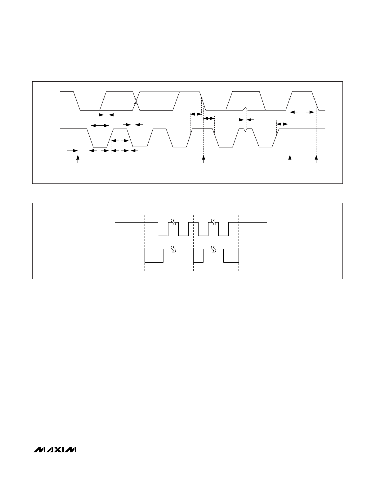
MAX9880A
Low-Power, High-Performance
Dual I2S Stereo Audio Codec
______________________________________________________________________________________ 59
SDA
Figure 14. 2-Wire Interface Timing Diagram
SCL
SDA
SSrP
Figure 15. START, STOP, and Repeated START Conditions
sequence is framed by a START or repeated START
condition, a not acknowledge, and a STOP condition.
SDA operates as both an input and an open-drain output. A pullup resistor, typically greater than 500Ω, is
required on SDA. SCL operates only as an input. A
pullup resistor, typically greater than 500Ω, is required
on SCL if there are multiple masters on the bus, or if the
single master has an open-drain SCL output. Series
resistors in line with SDA and SCL are optional. Series
resistors protect the digital inputs of the MAX9880A
from high voltage spikes on the bus lines and minimize
crosstalk and undershoot of the bus signals.
Bit Transfer
One data bit is transferred during each SCL cycle. The
data on SDA must remain stable during the high period
of the SCL pulse. Changes in SDA while SCL is high
are control signals (see the
START and STOP
Conditions
section).
START and STOP Conditions
SDA and SCL idle high when the bus is not in use. A
master initiates communication by issuing a START
condition. A START condition is a high-to-low transition
on SDA with SCL high. A STOP condition is a low-tohigh transition on SDA while SCL is high (Figure 15). A
START condition from the master signals the beginning
of a transmission to the MAX9880A. The master terminates transmission and frees the bus by issuing a STOP
condition. The bus remains active if a repeated START
condition is generated instead of a STOP condition.
Early STOP Conditions
The MAX9880A recognizes a STOP condition at any
point during data transmission except if the STOP condition occurs in the same high pulse as a START condition. For proper operation, do not send a STOP
condition during the same SCL high pulse as the
START condition.
t
LOW
t
SU,DAT
t
t
t
HD,DAT
SU,STA
t
HD,STA
t
SP
t
SU,STO
BUF
SCL
t
HD,STA
START CONDITION
t
HIGH
t
t
R
F
REPEATED START CONDITION
STOP
CONDITION
CONDITION
START

MAX9880A
Low-Power, High-Performance
Dual I2S Stereo Audio Codec
60 ______________________________________________________________________________________
Figure 16. Acknowledge
Figure 17. Writing 1 Byte of Data
Slave Address
The slave address is defined as the seven most significant bits (MSBs) followed by the read/write bit. For the
MAX9880A, the seven most significant bits are
0010000. Setting the read/write bit to 1 (slave address
= 0x21) configures the MAX9880A for read mode.
Setting the read/write bit to 0 (slave address = 0x20)
configures the MAX9880A for write mode. The address
is the first byte of information sent to the MAX9880A
after the START condition.
Acknowledge
The acknowledge bit (ACK) is a clocked 9th bit that the
MAX9880A uses to handshake receipt each byte of
data when in write mode (see Figure 16). The
MAX9880A pulls down SDA during the entire mastergenerated 9th clock pulse if the previous byte is successfully received. Monitoring ACK allows for detection
of unsuccessful data transfers. An unsuccessful data
transfer occurs if a receiving device is busy or if a system fault has occurred. In the event of an unsuccessful
data transfer, the bus master retries communication.
The master pulls down SDA during the 9th clock cycle
to acknowledge receipt of data when the MAX9880A is
in read mode. An acknowledge is sent by the master
after each read byte to allow data transfer to continue.
A not acknowledge is sent when the master reads the
final byte of data from the MAX9880A, followed by a
STOP condition.
Write Data Format
A write to the MAX9880A includes transmission of a
START condition, the slave address with the R/W bit set
to 0, 1 byte of data to configure the internal register
address pointer, 1 or more bytes of data, and a STOP
condition. Figure 17 illustrates the proper frame format
for writing 1 byte of data to the MAX9880A. Figure 18
illustrates the frame format for writing n bytes of data to
the MAX9880A.
The slave address with the R/W bit set to 0 indicates
that the master intends to write data to the MAX9880A.
The MAX9880A acknowledges receipt of the address
byte during the master-generated 9th SCL pulse.
START
CONDITION
ACKNOWLEDGE FROM MAX9880A
S AA
SCL
SDA
0SLAVE ADDRESS REGISTER ADDRESS
1
29
NOT ACKNOWLEDGE
ACKNOWLEDGE FROM MAX9880A
ACKNOWLEDGE
CLOCK PULSE FOR
ACKNOWLEDGMENT
ACKNOWLEDGE FROM MAX9880A
B1 B0B3 B2B5 B4B7 B6
DATA BYTE
P
A
R/W
1 BYTE
AUTOINCREMENT INTERNAL
REGISTER ADDRESS POINTER

MAX9880A
Low-Power, High-Performance
Dual I2S Stereo Audio Codec
______________________________________________________________________________________ 61
Figure 18. Writing n Bytes of Data
Figure 19. Reading 1 Byte of Data
The second byte transmitted from the master configures the MAX9880A’s internal register address pointer.
The pointer tells the MAX9880A where to write the next
byte of data. An acknowledge pulse is sent by the
MAX9880A upon receipt of the address pointer data.
The third byte sent to the MAX9880A contains the data
that is written to the chosen register. An acknowledge
pulse from the MAX9880A signals receipt of the data
byte. The address pointer autoincrements to the next
register address after each received data byte. This
autoincrement feature allows a master to write to
sequential registers within one continuous frame. The
master signals the end of transmission by issuing a
STOP condition. Register addresses greater than 0x17
are reserved. Do not write to these addresses.
Read Data Format
Send the slave address with the R/W bit set to 1 to initiate a read operation. The MAX9880A acknowledges
receipt of its slave address by pulling SDA low during
the 9th SCL clock pulse. A START command followed
by a read command resets the address pointer to register 0x00.
The first byte transmitted from the MAX9880A is the
contents of register 0x00. Transmitted data is valid on
the rising edge of SCL. The address pointer autoincrements after each read data byte. This autoincrement
feature allows all registers to be read sequentially within
one continuous frame. A STOP condition can be issued
after any number of read data bytes. If a STOP condition is issued followed by another read operation, the
first data byte to be read is from register 0x00.
The address pointer can be preset to a specific register
before a read command is issued. The master presets
the address pointer by first sending the MAX9880A’s
slave address with the R/W bit set to 0 followed by the
register address. A repeated START condition is then
sent followed by the slave address with the R/W bit set
to 1. The MAX9880A then transmits the contents of the
specified register. The address pointer autoincrements
after transmitting the first byte.
The master acknowledges receipt of each read byte
during the acknowledge clock pulse. The master must
acknowledge all correctly received bytes except the
last byte. The final byte must be followed by a not
acknowledge from the master and then a STOP condition. Figure 19 illustrates the frame format for reading 1
byte from the MAX9880A. Figure 20 illustrates the frame
format for reading multiple bytes from the MAX9880A.
ACKNOWLEDGE FROM MAX9880A
S
SLAVE ADDRESS
R/W
ACKNOWLEDGE FROM MAX9880A
S
0
R/W
ACKNOWLEDGE FROM MAX9880A
A
REGISTER ADDRESS
ACKNOWLEDGE FROM MAX9880A
A
ACKNOWLEDGE FROM MAX9880A
B1 B0B3 B2B5 B4B7 B6
A
DATA BYTE 1
1 BYTE
AUTOINCREMENT INTERNAL
REGISTER ADDRESS POINTER
ACKNOWLEDGE FROM MAX9880A
Sr 1SLAVE ADDRESS REGISTER ADDRESS SLAVE ADDRESS DATA BYTE
R/WREPEATED START
ACKNOWLEDGE FROM MAX9880A
A0
NOT ACKNOWLEDGE FROM MASTER
AA
B1 B0B3 B2B5 B4B7 B6
DATA BYTE n
1 BYTE
A
1 BYTE
AUTOINCREMENT INTERNAL
REGISTER ADDRESS POINTER
A
P
P

MAX9880A
Low-Power, High-Performance
Dual I2S Stereo Audio Codec
62 ______________________________________________________________________________________
Figure 20. Reading n Bytes of Data
Table 27. Clock Initialization (Perform Before Any Playback or Record Setup)
Table 28. Music Playback
Applications Information
Proper layout and grounding are essential for optimum
performance. When designing a PCB for the
MAX9880A, partition the circuitry so that the analog
sections of the MAX9880A are separated from the digital sections. This ensures that the analog audio traces
are not routed near digital traces.
Use a large continuous ground plane on a dedicated
layer of the PCB to minimize loop areas. Connect
AGND and DGND directly to the ground plane using
the shortest trace length possible. Proper grounding
improves audio performance, minimizes crosstalk
between channels, and prevents any digital noise from
coupling into the analog audio signals.
Ground the bypass capacitors on MICBIAS, REG,
PREG, and REF directly to the ground plane with minimum trace length. Also be sure to minimize the path
length to AGND. Bypass AVDD directly to AGND.
Connect all digital I/O termination to the ground plane
with minimum path length to DGND. Bypass DVDD and
DVDDS1 directly to DGND.
Route microphone signals from the microphone to the
MAX9880A as a differential pair, ensuring that the positive and negative signals follow the same path as
closely as possible with equal trace length. When using
single-ended microphones or other single-ended audio
sources, ground the negative microphone input as
close to the audio source as possible and then treat the
positive and negative traces as differential pairs.
The MAX9880A TQFN package features an exposed
thermal pad on its underside. Connect the exposed
thermal pad to AGND.
An evaluation kit (EV kit) is available to provide an
example layout for the MAX9880A. The EV kit allows
quick setup of the MAX9880A and includes easy-to-use
software allowing all internal registers to be controlled.
Startup Sequences
ACKNOWLEDGE FROM MAX9880A
S
R/W
ACKNOWLEDGE FROM MAX9880A
0
REPEATED START
ACKNOWLEDGE FROM MAX9880A
Sr 1SLAVE ADDRESS REGISTER ADDRESS SLAVE ADDRESS DATA BYTE
R/W
NOT ACKNOWLEDGE FROM MASTER
AAA
1 BYTE
AUTOINCREMENT INTERNAL
REGISTER ADDRESS POINTER
A
P
SEQUENCE DESCRIPTION REGISTERS
1 SHDN = 0 0x27
2 Configure clocks 0x05, 0x06, 0x07, 0x0B, 0x0C
3 Conf igure digital audio interface 0x08, 0x09, 0x0A, 0x0D, 0x0E, 0x0F
SEQUENCE DESCRIPTION REGISTERS
1 Select DAC audio source 0x10
2 Select music filters 0x11
3 Set output volume 0x1C, 0x1D
4 Set line output volume 0x1E, 0x1F
5 Select headphone mode 0x24
6 Enable line outputs and DAC as required 0x26
7 Enable LRCLK and BCLK (if operating in slave mode) N/A
8 Enable MAX9880A 0x27
9 Enable external amplifier (if using) N/A

MAX9880A
Low-Power, High-Performance
Dual I2S Stereo Audio Codec
______________________________________________________________________________________ 63
Table 29. Line Input Playback
Table 30. Line Input Playback with Record
Table 31. Voice Playback
SEQUENCE DESCRIPTION REGISTERS
1 Set line input gain 0x1A, 0x1B
2 Set volume 0x1C, 0x1D
3 Set line output volume (if using) 0x1E, 0x1F
4 Select headphone mode 0x24
5 Enable line outputs and line inputs as required 0x26
6 Enable MAX9880A 0x27
7 Enable external amplifier (if using) N/A
SEQUENCE DESCRIPTION REGISTERS
1 Select music filters 0x11
2 Set line input gain 0x1A, 0x1B
3 Set volume 0x1C, 0x1D
4 Set line output volume (if using) 0x1E, 0x1F
5 Conf igure ADC input m ixer 0x22
6 Select headphone mode 0x24
7 Enable line outputs, line inputs, and ADC as required 0x26
8 Enable LRCLK and BCLK (if operating in slave mode) N/A
9 Enable MAX9880A 0x27
10 Enable external amplifier (if using) N/A
SEQUENCE DESCRIPTION REGISTERS
1 Select DAC audio source 0x10
2 Select voice filters 0x11
3 Set volume 0x1C, 0x1D
4 Set line output volume (if using) 0x1E, 0x1F
5 Select headphone mode 0x24
6 Enable line outputs and DAC as required 0x26
7 Enable LRCLK and BCLK (if operating in slave mode) N/A
8 Enable MAX9880A 0x27
9 Enable external amplifier (if using) N/A

MAX9880A
Low-Power, High-Performance
Dual I2S Stereo Audio Codec
64 ______________________________________________________________________________________
Table 32. Voice Microphone Record
Table 33. Voice Playback with Record
SEQUENCE DESCRIPTION REGISTERS
1 Select voice filters 0x11
2 Set ADC level to 0dB 0x18, 0x19
3 Configure microphone gain 0x20, 0x21
4 Set line output volume (if using) 0x1E, 0x1F
5 Conf igure ADC input m ixer 0x22
6 Configure MICBIAS voltage 0x23
7 Enable ADC 0x26
8 Enable LRCLK and BCLK (if operating in slave mode) N/A
9 Enable MAX9880A 0x27
SEQUENCE DESCRIPTION REGISTERS
1 Select voice filters 0x11
2 Set ADC level to 0dB 0x18, 0x19
3 Configure microphone gain 0x20, 0x21
4 Set line output volume (if using) 0x1E, 0x1F
5 Conf igure ADC input m ixer 0x22
6 Configure MICBIAS voltage 0x23
7 Enable ADCs and DACs as required 0x26
8 Enable LRCLK and BCLK (if operating in slave mode) N/A
9 Enable MAX9880A 0x27

MAX9880A
Low-Power, High-Performance
Dual I2S Stereo Audio Codec
______________________________________________________________________________________ 65
Table 34. Music Playback
Table 35. Voice Duplex
Example of Register Settings for Music
Playback and Voice Duplex Senarios
Music Playback
f
MCLK
= 12.288MHz (master clock supplied to codec),
f
LRCLK
= 48kHz, standard I2S format, codec in slave
mode, music source connected through S2 pins to
DAI2 audio path, and output on headphone amplifiers
(output capacitorless mode).
Voice Duplex
f
MCLK
= 13MHz (master clock supplied to codec),
f
LRCLK
= 8kHz, TDM/PCM format, codec in slave
mode, voice signals on S1 pins to DAI1 audio path and
output on headphone amplifier left (differential mode).
SEQUENCE DESCRIPTION REGISTER ADDRESS REGISTER VALUE
1 SHDN = 0 0x27 04h
2 Configure system clock 0x05 10h
3 Configure DAI2 clock 0x0B 60h
4 Configure DAI2 clock 0x0C 00h
5 Conf igure D AI2 audio path 0x0D 11h
6 Conf igure D AI2 audio path 0x0E 50h
7 Select DAC audio source 0x10 21h
8 Select mu sic filters 0x11 80h
9 Set output volume (0dB) 0x1C, 0 x1D 09h
10 Set line output vo lume (muted) 0x1E, 0 x1F 40h
11 Select headphone mode (output capacitorless mode) 0x24 02h
12 Enable line outputs and DAC as required 0x26 0Ch
13 Enable MAX9880A 0x27 84h
SEQUENCE DESCRIPTION REGISTER ADDRESS REGISTER VALUE
1 SHDN = 0 0x27 04h
2 Configure system clock 0x05 10h
3 Configure DAI1 clock 0x0B 0Fh
4 Configure DAI1 clock 0x0C 1Fh
5 Conf igure D AI1 audio path 0x0D 04h
6 Conf igure D AI2 audio path 0x0E 30h
7 Select DAC audio source 0x10 21h
8 Select vo ice GSM filters 0x11 33h
9 Set ADC le ve l to 0dB 0x18, 0x19 03h
10 Configure microphone gain (20dB preamp gain) 0x20, 0 x21 54h
11 Set headphone vo lume 0x1C, 0 x1D 09h
12 Set line output vo lume (if using) 0x1E, 0x1F 40h
13 Configure ADC input mi xer 0x22 50h
14 Configure MICBIAS voltage (2.2V) 0x23 01h
15 Select headphone mode 0x24 01h
16 Enable line outputs, ADC and DAC as required 0x26 0Bh
17 Enable MAX9880A 0x27 84h

MAX9880A
Low-Power, High-Performance
Dual I2S Stereo Audio Codec
66 ______________________________________________________________________________________
/
Functional Diagram/Typical Operating Circuit
X1
1µF
1.8V
1µF
1µF
1.8V
1µF
1.8V
SDOUTS2
SDINS2
LRCLKS2
BCLKS2
SDOUTS1
SDINS1
LRCLKS1
BCLKS1
MCLK
DOUT
SDA/DIN
CS
SCL/SCLK
MODE
IRQ
1µF
1.8V
1.8V
1µF
PVDD
PREG
AVDD
DVDD
MICVDD
DVDDS1
3
34
(E3, F3)
12
(A7)
9
(A6)
46
(B1)
42
(D2)
43
(C1)
44
(C2)
45
(C3)
37
(F1)
38
(D3)
39
(E1)
40
(E2)
41
(D1)
6
(B5)
1
(B2)
5
(B4)
2
(B3)
7
(A5)
8
(A4)
16
(B7)
36
(F2)
(A2)4(A3)
OSC
XTAL
XTEN,
XTOSC
REG
LINEAR
AUDIO SOURCE SELECTION SEL1, SEL2
GEN
CLOCK
C/SPI
2
I
REF
10
(B6)
REF
2.2µF
X2
(8kHz TO 96kHz)
DIGITAL AUDIO PATH 2
(8kHz TO 48kHz)
DIGITAL AUDIO PATH 1
FREQ1
PSCLK
SPDMCLK
VOLL:
_DACA:
PLL2, NI2,
REGS 0D-0F
PLL1, NI1,
REGS 08-OA
13
(C6)
REG
1µF
MIXSPDML
DCB
AUDIO
+6dB TO -84dB
0dB TO -15dB
VCM PREG
MICBIAS
17
1µF
SPDML
MIX
FILTER
MIX/MUX
(B8)
MICBIAS
SPDMDATA
1b
DCB
VOLR:
+6dB TO -84dB
_DACA:
0dB TO -15dB
I/F
SPDMR
MIX
MIXSPDMR
AUDIO
FILTER
DVST:
MAX9880A
-9dB TO -69dB
DSTS
MIX/MUX
PGAML:
PALEN:
LOUTP
32
(E4)31(F4)
HPMODE
MIXDAL
VOICE/AUDIO
VOLL:
+6dB TO -84dB
_DACA:
0dB TO -15dB
VDACG:
0/6/12/18dB
AVL:
+4dB TO -11dB
MODEADLEN
VOICE/AUDIO
MXINL
+20dB TO 0dB
0/20/30dB
19
(D7)18(C7)
MICLP/
DIGMICDATA
DAC
MIX
FILTER
FILTER
ADCL
MIX
MICLN/
LOUTN
DALEN
MODE, DVFLT
MIX/MUX
AVLG:
AVFLT
DIGMICCLK
29
HPMODE
MIXDAR
VOLR:
_DACA:
VDACG:
0/6/12/18dB
ROUTP
(E5)
DAC
MIX
FILTER
VOICE/AUDIO
+6dB TO -84dB
0dB TO -15dB
0/6/12/18dB
SPDMDATA
ROUTN
30
(F5)
DAREN
MODE, DVFLT
AVR:
PGAMR:
+20dB TO 0dB
PAREN:
0/20/30dB
20
(C8)
MICRP/
SPDMDATA
LOUTL
26
(E7)
LOLEN
LOGL:
0dB TO -30dB
+4dB TO -11dB
MODE
FILTER
VOICE/AUDIO
ADCR
MIX
MIXINR
21
MICRN/
AVRG:
AVFLTADREN
SPDMCLK
(D8)
SPDMCLK
0/6/12/18dB
LIGL:
+30dB TO 0dB
23
JACKSNS
AUX
LOUTR
22
25
(F7)
(D5)
LOREN
SENSE
LNREN
AUXEN
HEADPHONE
27
(E6, F6)
15
(A8)
47
(A1)
PGND
AGND
DGND
LOGR:
0dB TO -30dB
LNLEN
LIGR:
+30dB TO 0dB
(E8)
24
(F8)
LINL
LINR
RECEIVER
FM

MAX9880A
Low-Power, High-Performance
Dual I2S Stereo Audio Codec
______________________________________________________________________________________ 67
Package Information
For the latest package outline information and land patterns (footprints), go to www.maxim-ic.com/packages. Note that a “+”, “#”, or
“-” in the package code indicates RoHS status only. Package drawings may show a different suffix character, but the drawing pertains to the package regardless of RoHS status.
PACKAGE TYPE PACKAGE CODE OUTLINE NO.
LAND
PATTERN NO.
48 TQFN-EP T4866+1
21-0141
90-0057
48 WLP W482A3+1
21-0230
Refer to Application Note 1891

MAX9880A
Low-Power, High-Performance
Dual I2S Stereo Audio Codec
68 ______________________________________________________________________________________
Package Information (continued)
For the latest package outline information and land patterns (footprints), go to www.maxim-ic.com/packages. Note that a “+”, “#”, or
“-” in the package code indicates RoHS status only. Package drawings may show a different suffix character, but the drawing pertains to the package regardless of RoHS status.

MAX9880A
Low-Power, High-Performance
Dual I2S Stereo Audio Codec
______________________________________________________________________________________ 69
Package Information (continued)
For the latest package outline information and land patterns (footprints), go to www.maxim-ic.com/packages. Note that a “+”, “#”, or
“-” in the package code indicates RoHS status only. Package drawings may show a different suffix character, but the drawing pertains to the package regardless of RoHS status.

MAX9880A
Low-Power, High-Performance
Dual I2S Stereo Audio Codec
Maxim cannot assume responsibility for use of any circuitry other than circuitry entirely embodied in a Maxim product. No circuit patent licenses are
implied. Maxim reserves the right to change the circuitry and specifications without notice at any time.
70
____________________Maxim Integrated Products, 120 San Gabriel Drive, Sunnyvale, CA 94086 408-737-7600
© 2011 Maxim Integrated Products Maxim is a registered trademark of Maxim Integrated Products, Inc.
Revision History
REVISION
NUMBER
0 7/10 Init ia l release —
1 3/11 Various data sheet errors
REVISION
DATE
DESCRIPTION
PAGES
CHANGED
15–22, 24, 29, 31,
47, 49, 51, 52,
55–58, 60, 61,
62, 66
 Loading...