

General Description
The MAX9879 combines a high-efficiency stereo Class D
audio power amplifier with a stereo capacitor-less
DirectDrive®headphone amplifier. Maxim’s filterless class
D amplifiers with active emissions limiting technology provide Class AB performance with Class D efficiency.
The Class D power amplifier delivers up to 715mW from
a 3.7V supply into an 8Ω load with 88% efficiency to
extend battery life. The filterless modulation scheme
combined with active emission limiting circuitry and
spread-spectrum modulation greatly reduces EMI while
eliminating the need for output filtering used in traditional Class D devices.
The headphone amplifier delivers up to 58mW from
a 3.7V supply into a 16Ω load. Maxim’s DirectDrive
architecture produces a ground-referenced output from
a single supply, eliminating the need for large DCblocking capacitors, saving cost, space and component height.
The device utilizes a user-defined input architecture,
three preamplifier gain settings, an input mixer, volume
control, comprehensive click-and-pop suppression, and
I
2
C control. A bypass mode feature disables the integrated Class D amplifier and utilizes an internal DPST switch
to allow an external amplifier to drive the speaker that is
connected at the outputs of the MAX9879.
The MAX9879 is available in a thermally efficient,
space-saving 30-bump UCSP™ package.
Applications
Features
♦ Better than 9dB Margin Under EN 55022 Class B
Limits with No Filter Components
♦ Low RF Susceptibility Design Rejects TDMA
Noise from GSM Radios
♦ Input Mixer with User Defined Input Mode
♦ Stereo 715mW Speaker Output (R
L
= 8Ω,
V
DD
= 3.7V)
♦ Stereo 58mW Headphone Output (16Ω,
V
DD
= 3.7V)
♦ Low 0.04% THD+N at 1kHz (Class D Power
Amplifier)
♦ Low 0.018% THD+N at 1kHz (Headphone
Amplifier)
♦ 88% Efficiency (R
L
= 8Ω, P
OUT
= 750mW)
♦ 1.6Ω Analog Switch for Speaker Amplifier Bypass
♦ High Speaker Amplifier PSRR (72dB at 217Hz)
♦ High Headphone Amplifier PSRR (84dB at 217Hz)
♦ I
2
C Control
♦ Hardware and Software Shutdown Mode
♦ Ultra-Low Click and Pop
♦ Robust Design with Current and Thermal
Protection
♦ Available in Space-Saving Package
5x6 UCSP (2.5mm x 3mm)
MAX9879
Stereo Class D Audio Subsystem
with DirectDrive Headphone Amplifier
________________________________________________________________
Maxim Integrated Products
1
MIXER
PREAMPLIFIER
SINGLE SUPPLY
2.7V TO 5.5V
I2C
INTERFACE
VOLUME
CONTROL
VOLUME
CONTROL
BYPASS
MAX9879
Simplified Block Diagram
OUTL- PVDDL
OUTL+
C1P
1
A
B
C
D
E
2
3
4
PGNDR
RXIN- PGNDL
RXIN+
C1N
PGNDR
GND GND
GND
V
SS
GND
BIAS INB1
INA1
HPL
SCL
56
TOP VIEW
(BUMP SIDE DOWN)
OUTR-
PVDDR
OUTR+
SDA
V
DD
INB2
INA2
HPR
SHDN
V
CCIO
Pin Configuration
19-4436; Rev 0; 2/09
For pricing, delivery, and ordering information, please contact Maxim Direct at 1-888-629-4642,
or visit Maxim’s website at www.maxim-ic.com.
EVALUATION KIT
AVAILABLE
Ordering Information
PART
PIN - PA C K A G E
MAX9879ERV+
30 UCSP (5x6)
+
Denotes a lead(Pb)-free/RoHS-compliant package.
Cell Phones
Portable Multimedia Players
DirectDrive is a registered trademark of Maxim Integrated
Products, Inc.
UCSP is a trademark of Maxim Integrated Products, Inc.
TEMP RANGE
-40°C to +85°C
MAX9879
Stereo Class D Audio Subsystem
with DirectDrive Headphone Amplifier
2 _______________________________________________________________________________________
ABSOLUTE MAXIMUM RATINGS
VDD, PVDDL, PVDDR to GND ..................................-0.3V to +6V
V
DD
, PVDDL to PVDDR .........................................-0.3V to +0.3V
V
DD
to PVDDL .......................................................-0.3V to +0.3V
V
CCIO
to GND...........................................................-0.3V to +4V
PGNDL, PGNDR, to GND......................................-0.3V to +0.3V
PGNDL to PGNDR.................................................-0.3V to +0.3V
V
SS
to GND...............................................................-6V to +0.3V
C1N to GND ................................................(V
SS
- 0.3V) to +0.3V
C1P to GND ...........................................-0.3V to (PVDD_ + 0.3V)
HPL, HPR to V
SS
(Note 1).............................-0.3V to the lower of
(V
DD
- V
SS
+ 0.3V) or +9V
HPL, HPR to V
DD
(Note 2) .........................+0.3V to the higher of
(V
SS
- PVDD_ - 0.3V) or -9V
INA1, INA2, INB1, INB2, BIAS..................................-0.3V to +4V
SDA, SCL, SHDN......................................................-0.3V to +4V
All Other Pins to GND ............................-0.3V to (PVDD_ + 0.3V)
Continuous Current In/Out of PVDD_, PGND_, OUT_ ....±800mA
Continuous Current In/Out of HPR and HPL .....................140mA
Continuous Current In/Out of RXIN+ and RXIN- ...............150mA
Continuous Input Current V
SS
...........................................100mA
Continuous Input Current (All Other Pins) ........................±20mA
Duration of OUT_ Short Circuit
to PGND_ or PVDD_...............................................Continuous
Duration of Short Circuit
Between OUT_+ and OUT_- ..................................Continuous
Duration of HP_ Short Circuit to GND or PVDDL........Continuous
Continuous Power Dissipation (T
A
= +70°C)
5x6 UCSP Multilayer Board
(derate 16.5mW/°C above +70°C).............................1250mW
Junction Temperature......................................................+150°C
Operating Temperature Range ...........................-40°C to +85°C
Storage Temperature Range .............................-65°C to +150°C
Lead Temperature (soldering, 10s) .................................+300°C
ELECTRICAL CHARACTERISTICS
(VDD= V
PVDDL
= V
PVDDR
= 3.7V, V
CCIO
= 1.8V, V
GND
= V
PGNDL
= V
PGNDR
= 0. Single-ended inputs, preamp = 0, volume controls =
0dB, BYPASS = 0, SHDN = 1. Speaker loads connected between OUT_+ and OUT_-. Headphone loads connected from HPL or HPR to
GND. R
SPK
= ∞, RHP= ∞. C1 = C2 = C
BIAS
= 1µF. TA= T
MIN
to T
MAX
, unless otherwise noted. Typical values are at TA= +25°C.)
(Notes 3, 4)
Stresses beyond those listed under “Absolute Maximum Ratings” may cause permanent damage to the device. These are stress ratings only, and functional
operation of the device at these or any other conditions beyond those indicated in the operational sections of the specifications is not implied. Exposure to
absolute maximum rating conditions for extended periods may affect device reliability.
Note 1: HPR and HPL should be limited to no more than 9V above VSS, or above PVDD+ 0.3V, whichever limits first.
Note 2: HPR and HPL should be limited to no more than 9V below PV
DD
, or below VSS- 0.3V, whichever limits first.
Analog Supply Voltage Range
Digital Supply Voltage Range V
Quiescent Current I
Shutdown Current I
Turn-On Time t
Input Resistance R
PARAMETER SYMBOL CONDITIONS MIN TYP MAX UNITS
V
,
DD
PVDDR
Guaranteed by PSRR Test 2.7 5.5 V
PVDDL
CCIO
1.7 3.6 V
HP mode, RHP = ∞ 5.6 9.0
DD
SHDN
ON
IN
Stereo SPK mode, R
Mono SPK mode, R
Stereo SPK + HP mode, RHP= R
I
= IDD + I
SHDN
I
+ ICC; TA = +25°C
PVDDL
PVDDR
Time from shutdown or power-on to full
operation
TA = +25°C, preamp = 0dB or +5.5dB 11 21 31
TA = +25°C, preamp = +20dB 3 5.5 8
= ∞ 9.8 18
SPK
= ∞ 6.6 10
SPK
= ∞ 13.2 24
SPK
Software
shutdown
+
Hardware
shutdown
510
0.1 1
10 ms
Preamp = 0 2.3
Preamp = +5.5dB 1.2Maximum Input Signal Swing
Preamp = +20dB 0.230
mA
V
µA
kΩ
P-P
MAX9879
Stereo Class D Audio Subsystem
with DirectDrive Headphone Amplifier
_______________________________________________________________________________________ 3
ELECTRICAL CHARACTERISTICS (continued)
(VDD= V
PVDDL
= V
PVDDR
= 3.7V, V
CCIO
= 1.8V, V
GND
= V
PGNDL
= V
PGNDR
= 0. Single-ended inputs, preamp = 0, volume controls =
0dB, BYPASS = 0, SHDN = 1. Speaker loads connected between OUT_+ and OUT_-. Headphone loads connected from HPL or HPR to
GND. R
SPK
= ∞, RHP= ∞. C1 = C2 = C
BIAS
= 1µF. TA= T
MIN
to T
MAX
, unless otherwise noted. Typical values are at TA= +25°C.)
(Notes 3, 4)
Common-Mode Rejection Ratio CMRR
Input DC Voltage IN__ inputs 1.22 1.3 1.38 V
Bias Voltage V
SPEAKER AMPLIFIER
Output Offset Voltage V
Click-and-Pop Level K
Power-Supply Rejection Ratio
(Note 5)
Total Harmonic Distortion + Noise THD+N
Signal-to-Noise Ratio SNR
Output Frequency
PARAMETER SYMBOL CONDITIONS MIN TYP MAX UNITS
BIAS
OS
CP
PSRR T
OUT
f
= 1kHz (differential
IN
input mode)
TA = +25°C (volume at mute) ±0.5 ±4 mV
TA = + 25° C ( vol um e at 0d B, E N A = 1 and
E N B = 0 or E N B = 1 and E N A = 0, ΔIN _ = 0)
Peak voltage,
= +25°C
T
A
A-weighted, 32 samples
per second, volume at
mute (Note 5)
= +25°C
A
THD+N ≤ 1%, R
8Ω
f = 1kHz, P
R
= 8Ω
SPK
A-weighted, ENA = 1
and ENB = 0 or ENB = 1
and ENA = 0
A-weighted ENA =
ENB = 1
=
SPK
= 350mW, TA = +25°C,
OUT
Preamp = 0 58
Preamp = 5.5dB 55
Preamp = 20dB 43
1.13 1.2 1.272 V
±4.5 mV
Into shutdown -70
Out of shutdown -70
PVDD_ = V
= 2.7V to 5.5V
f = 217Hz,
100mV
f = 1kHz,
100mV
f = 20kHz,
100mV
VDD = 3.7V 715
VDD = 3.3V 565Output Power P
V
DD
ΔIN_ = 0
(single-ended)
ΔIN_ = 1
(differential)
ΔIN_ = 0
(single-ended)
ΔIN_ = 1
(differential)
DD
ripple
P-P
ripple
P-P
ripple
P-P
= 3.0V 470
50 76
72
68
55
0.04 0.2 %
92
94
88
92
700
±40
dB
dBV
dB
mW
dB
kHz
MAX9879
Stereo Class D Audio Subsystem
with DirectDrive Headphone Amplifier
4 _______________________________________________________________________________________
ELECTRICAL CHARACTERISTICS (continued)
(VDD= V
PVDDL
= V
PVDDR
= 3.7V, V
CCIO
= 1.8V, V
GND
= V
PGNDL
= V
PGNDR
= 0. Single-ended inputs, preamp = 0, volume controls =
0dB, BYPASS = 0, SHDN = 1. Speaker loads connected between OUT_+ and OUT_-. Headphone loads connected from HPL or HPR to
GND. R
SPK
= ∞, RHP= ∞. C1 = C2 = C
BIAS
= 1µF. TA= T
MIN
to T
MAX
, unless otherwise noted. Typical values are at TA= +25°C.)
(Notes 3, 4)
Current Limit 1.5 A
Efficiency η P
Speaker Gain A
Output Noise
Crosstalk
HEADPHONE AMPLIFIERS
Output Offset Voltage V
Click-and-Pop Level K
Power-Supply Rejection Ratio
(Note 5)
Output Power P
Headphone Gain A
Channel-to-Channel Gain
Tracking
PARAMETER SYMBOL CONDITIONS MIN TYP MAX UNITS
V
OS T
CP
PSRR T
OUT
V
= 600mW, f = 1kHz 88 %
OUT
A-weighted, (ENA = 1 and ENB = 0
or ENA = 0 and ENB = 1), ΔIN_ = 0
OUTL to OUTR, OUTR to OUTL,
f = 20Hz to 20kHz
TA = +25°C (volume at mute) ±0.22 ±0.85 mV
= + 25° C ( V ol um e at 0d B, E N A = 1 and
A
E N B = 0 or E N A = 0 and E N B = 1, ΔIN _ = 0)
Peak voltage, TA = 25°C
A-weighted, 32 samples
per second, volume at
mute (Note 5)
= +25°C
A
THD+N = 1%
T
= +25°C, HPL to HPR, volume at 0dB,
A
ENA=1 and ENB = 0 or ENA = 1 and ENB
= 0, ΔIN_ = 0
17.4 18 18.4 dB
63 µV
75 dB
±1.5 mV
Into shutdown -75
Out of shutdown -75
PVDD_ = V
= 2.7V to 5.5V
f = 217Hz,
V
RIPPLE
= 100mV
f = 1kHz,
V
RIPPLE
= 100mV
f = 20kHz,
V
RIPPLE
= 100mV
RHP = 16Ω 58
R
HP
DD
P-P
P-P
P-P
= 32Ω 54
70 85
84
80
62
2.6 3 3.4 dB
±0.3 ±2.5 %
RMS
dBV
dB
mW
Total Harmonic Distortion + Noise THD+N
RHP = 32Ω
= 10mW, f = 1kHz)
(P
OUT
R
= 16Ω
HP
= 10mW, f = 1kHz)
(P
OUT
0.018
0.037 0.08
%
MAX9879
Stereo Class D Audio Subsystem
with DirectDrive Headphone Amplifier
_______________________________________________________________________________________ 5
ELECTRICAL CHARACTERISTICS (continued)
(VDD= V
PVDDL
= V
PVDDR
= 3.7V, V
CCIO
= 1.8V, V
GND
= V
PGNDL
= V
PGNDR
= 0. Single-ended inputs, preamp = 0, volume controls =
0dB, BYPASS = 0, SHDN = 1. Speaker loads connected between OUT_+ and OUT_-. Headphone loads connected from HPL or HPR to
GND. R
SPK
= ∞, RHP= ∞. C1 = C2 = C
BIAS
= 1µF. TA= T
MIN
to T
MAX
, unless otherwise noted. Typical values are at TA= +25°C.)
(Notes 3, 4)
Signal-to-Noise Ratio SNR
Slew Rate SR 0.35 V/µs
Capacitive Drive C
Crosstalk HPL to HPR, HPR to HPL, f = 20Hz to 20kHz 67 dB
Charge-Pump Frequency
VOLUME CONTROL
Minimum Setting _VOL = 1 -75 dB
Maximum Setting _VOL = 31 0 dB
Mute Attenuation f = 1kHz, _VOL = 0
Zero-Crossing Detection Time
Out
ANALOG SWITCH
On-Resistance R
Total Harmonic Distortion + Noise
Off-Isolation
DIGITAL INPUTS (SDA, SCL, SHDN)
Input Voltage High (SDA, SCL) V
Input Voltage Low (SDA, SCL) V
Input Hysteresis (SDA, SCL) V
PARAMETER SYMBOL CONDITIONS MIN TYP MAX UNITS
L
ON
IH
IL
HYS
A-weighted,
R
= 16Ω
HP
ZCD = 1 60 ms
I
= 20mA,
RXIN__
RXIN_ = 0 and V
BYPASS = 1
V
DIFRXIN
V
CMRXIN
f = 1kHz, BYPASS = 1
BYPASS = 0, RXIN+ and RXIN- to GND =
50Ω, R
SPK
speaker output signal
ENA = 1 and
ENB = 0 or
ENA = 1 and
ENB = 0
ENA = 1 and
ENB = 1
DD,
= 2V
= VDD/2,
,
P-P
= 8Ω, f = 10kHz, referred to
PGAIN_ = 00 0
PGAIN_ = 01 5.5Input Gain Input A or B
PGAIN_ = 10 20
Speaker 100
Headphone 110
TA = +25°C 2.4 4
= T
T
A
MIN
Series resistance is
10Ω per switch
No series resistors 0.3
ΔIN_ = 0 98
ΔIN_ = 1 98
ΔIN_ = 0 96
ΔIN_ = 1 96
100 pF
350
±20
to T
MAX
0.3 0.25 %
88 dB
0.7 x
V
CCIO
200 mV
5.2
0.3 x
V
CCIO
dB
kHz
dB
dB
Ω
V
V
MAX9879
Stereo Class D Audio Subsystem
with DirectDrive Headphone Amplifier
6 _______________________________________________________________________________________
ELECTRICAL CHARACTERISTICS (continued)
(VDD= V
PVDDL
= V
PVDDR
= 3.7V, V
CCIO
= 1.8V, V
GND
= V
PGNDL
= V
PGNDR
= 0. Single-ended inputs, preamp = 0, volume controls =
0dB, BYPASS = 0, SHDN = 1. Speaker loads connected between OUT_+ and OUT_-. Headphone loads connected from HPL or HPR to
GND. R
SPK
= ∞, RHP= ∞. C1 = C2 = C
BIAS
= 1µF. TA= T
MIN
to T
MAX
, unless otherwise noted. Typical values are at TA= +25°C.)
(Notes 3, 4)
Input Voltage High (SHDN) V
Input Voltage Low (SHDN) V
Input Hysteresis (SHDN) V
SDA, SCL, SHDN Input
Capacitance
Input Leakage Current I
Input Leakage Current I
DIGITAL OUTPUTS (SDA open drain)
Output Low-Voltage SDA V
Output High-Voltage SDA V
Output Fall Time SDA t
2-WIRE INTERFACE TIMING
External Pullup Voltage Range
(SDA and SCL)
Serial-Clock Frequency f
Bus Free Time Between STOP
and START Conditions
START Condition Hold t
START Condition Setup Time t
Clock Low Period t
Clock High Period t
Data Setup Time t
Data Hold Time t
SCL/SDA Receiving Rise Time t
SCL/SDA Receiving Fall Time t
SDA Transmitting Fall Time t
PARAMETER SYMBOL CONDITIONS MIN TYP MAX UNITS
1.4 V
0.4 V
100 mV
10 pF
V
-
CCIO
0.4
250 ns
HYS
C
IN
IN
OL
OH
OF
IH
IL
IN
SDA, SCL, SHDN, TA = +25°C ±1.0 µA
V
= 0, TA = +25°C ±1.0 µA
CCIO
I
= 3mA 0.4 V
SINK
I
= 3mA
SINK
V
to V
H(MIN)
= 10pF to 400pF, I
bus capacitance
L(MAX)
SINK
= 3mA
1.7 3.6 V
SCL
t
BUF
HD:STA
SU:STA
LOW
HIGH
SU:DAT
HD:DAT
R
F
F
(Note 6)
V
=1.8V (Note 6)
CCIO
V
= 3.6V (Note 6)
CCIO
DC 400 kHz
1.3 µs
0.6 µs
0.6 µs
1.3 µs
0.6 µs
100 ns
0 900 ns
20 +
0.1 x C
20 +
0.1 x C
20 +
0.1 x C
20 +
0.05 x C
B
B
B
B
300 ns
300 ns
250
250
V
ns
MAX9879
Stereo Class D Audio Subsystem
with DirectDrive Headphone Amplifier
_______________________________________________________________________________________ 7
Note 3: All devices are 100% production tested at TA= +25°C. All temperature limits are guaranteed by design.
Note 4: Class D amplifier testing performed with a resistive load in series with an inductor to simulate an actual speaker load. For
R
SPKR
= 8Ω, L = 68mH.
Note 5: Amplifier inputs are AC-coupled to GND.
Note 6: C
B
is in pF.
ELECTRICAL CHARACTERISTICS (continued)
(VDD= V
PVDDL
= V
PVDDR
= 3.7V, V
CCIO
= 1.8V, V
GND
= V
PGNDL
= V
PGNDR
= 0. Single-ended inputs, preamp = 0dB, volume controls =
0dB, BYPASS = 0, SHDN = 1. Speaker loads connected between OUT_+ and OUT_-. Headphone loads connected from HPL or HPR to
GND. R
SPK
= ∞, RHP= ∞. C1 = C2 = C
BIAS
= 1µF. TA= T
MIN
to T
MAX
, unless otherwise noted. Typical values are at TA= +25°C.)
(Notes 3, 4)
Set-Up Time for STOP Condition t
Pulse Width of Spike Suppressed t
Capacitive Load for Each Bus
Line
PARAMETER SYMBOL CONDITIONS MIN TYP MAX UNITS
SU:STO
SP
C
B
0.6 µs
050ns
400 pF
MAX9879
Stereo Class D Audio Subsystem
with DirectDrive Headphone Amplifier
8 _______________________________________________________________________________________
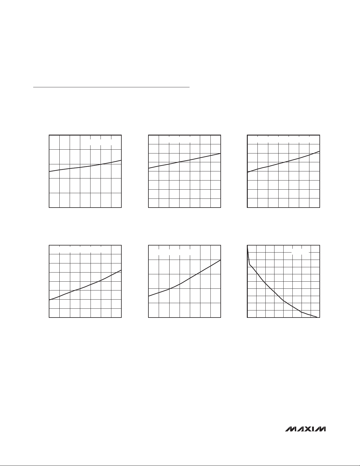
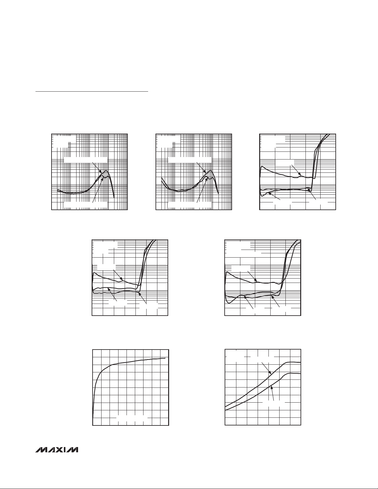
Typical Operating Characteristics
(VDD= V
PVDDL
= V
PVDDR
= 3.7V, V
CCIO
= 1.8V, V
GND
= V
PGNDL
= V
PGNDR
= 0. Single-ended inputs, preamp = 0dB, volume con-
trols = 0dB, BYPASS = 0, SHDN = 1. Speaker loads connected between OUT_+ and OUT_-. Headphone loads connected from HPL
or HPR to GND. R
SPK
= ∞, RHP= ∞. C1 = C2 = C
BIAS
= 1µF. TA= +25°C, unless otherwise noted.)
GENERAL
SUPPLY CURRENT vs. SUPPLY VOLTAGE
10
8
6
4
SUPPLY CURRENT (mA)
2
0
2.7 5.5
SUPPLY VOLTAGE (V)
HEADPHONE MODE
3.93.53.1 4.3 4.7 5.1
MAX9879 toc01
SUPPLY CURRENT (mA)
SUPPLY CURRENT vs. SUPPLY VOLTAGE
16
14
12
10
8
6
4
2
0
STEREO-SPEAKER MODE
2.7 5.5
3.93.53.1 4.3 4.7 5.1
SUPPLY VOLTAGE (V)
20
18
MAX9879 toc02
16
14
12
10
SUPPLY CURRENT (mA)
SUPPLY CURRENT vs. SUPPLY VOLTAGE
HEADPHONE + STEREO-SPEAKER MODE
8
6
4
2.7 5.5
3.93.53.1 4.3 4.7 5.1
SUPPLY VOLTAGE (V)
MAX9879 toc03
SUPPLY CURRENT vs. SUPPLY VOLTAGE
16
SOFTWARE-SHUTDOWN MODE
14
12
10
8
6
SUPPLY CURRENT (µA)
4
2
0
2.7 5.5
3.93.53.1 4.3 4.7 5.1
SUPPLY VOLTAGE (V)
50
MAX9879 toc04
40
30
20
SUPPLY CURRENT (nA)
10
SUPPLY CURRENT vs. SUPPLY VOLTAGE
HARDWARE-SHUTDOWN MODE
0
2.7 5.5
3.93.53.1 4.3 4.7 5.1
SUPPLY VOLTAGE (V)
MAX9879 toc05
ATTENUATION (dB)
VOLUME LEVEL vs. VOLUME STEP
100
90
80
70
60
50
40
30
20
10
0
032
VOLUME STEP
fIN = 1kHz
MAX9879 toc06
20 2812 1648 24
MAX9879
Stereo Class D Audio Subsystem
with DirectDrive Headphone Amplifier
_______________________________________________________________________________________ 9
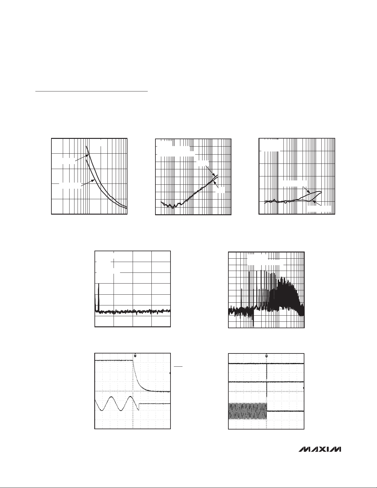
Typical Operating Characteristics (continued)
(VDD= V
PVDDL
= V
PVDDR
= 3.7V, V
CCIO
= 1.8V, V
GND
= V
PGNDL
= V
PGNDR
= 0. Single-ended inputs, preamp = 0dB, volume con-
trols = 0dB, BYPASS = 0, SHDN = 1. Speaker loads connected between OUT_+ and OUT_-. Headphone loads connected from HPL
or HPR to GND. R
SPK
= ∞, RHP= ∞. C1 = C2 = C
BIAS
= 1µF. TA= +25°C, unless otherwise noted.)
SPEAKER AMPLIFIERS (Headphone Disabled)
EFFICIENCY vs. OUTPUT POWER
MAX9879 toc12
OUTPUT POWER (mW)
EFFICIENCY (%)
700400 800600200100 300 500
50
70
80
20
60
10
30
40
90
100
0
0 900
fIN = 1kHz, RL = 8Ω
10
1
THD+N (%)
0.1
0.01
0.01 100
THD+N vs. FREQUENCY SPEAKER
PVDD_= 3.7V
= 8Ω
R
L
OUTPUT POWER = 200mW
OUTPUT POWER = 600mW
10.1 10
FREQUENCY (kHz)
THD+N vs. OUTPUT POWER
10
PVDD_ = 3.0V
= 8Ω
R
L
1
fIN = 6kHz
MAX9879 toc07
THD+N vs. FREQUENCY SPEAKER
10
PVDD_= 3.0V
= 8Ω
R
L
1
THD+N (%)
0.1
0.01
OUTPUT POWER = 100mW
OUTPUT POWER = 400mW
0.01 100
MAX9879 toc10
10.1 10
FREQUENCY (kHz)
10
1
MAX9879 toc08
PVDD_ = 3.7V
= 8Ω
R
L
LEFT SPEAKER ONLY
fIN = 6kHz
10
PVDD_ = 3.7V
= 8Ω
R
L
1
THD+N (%)
0.1
0.01
0 1000600
fIN = 6kHz
fIN = 20Hz
OUTPUT POWER (mW)
THD+N vs. OUTPUT POWER
THD+N vs. OUTPUT POWER
fIN = 1kHz
800200 400
MAX9879 toc11
MAX9879 toc09
THD+N (%)
0.1
0.01
0 700300 400100
fIN = 20Hz
200 500 600
OUTPUT POWER (mW)
fIN = 1kHz
THD+N (%)
0.1
0.01
0 1000800200 400
fIN = 20Hz
OUTPUT POWER (mW)
fIN = 1kHz
600
OUTPUT POWER vs. SUPPLY VOLTAGE
2000
RL = 8Ω
1800
1600
1400
1200
1000
OUPUT POWER (mW)
= 1kHz
f
IN
800
600
400
200
0
2.7 5.5
THD+N = 10%
THD+N = 1%
3.5 4.33.93.1 4.7 5.1
SUPPLY VOTAGE (V)
MAX9879 toc13
MAX9879
Stereo Class D Audio Subsystem
with DirectDrive Headphone Amplifier
10 ______________________________________________________________________________________
Typical Operating Characteristics (continued)
(VDD= V
PVDDL
= V
PVDDR
= 3.7V, V
CCIO
= 1.8V, V
GND
= V
PGNDL
= V
PGNDR
= 0. Single-ended inputs, preamp = 0dB, volume con-
trols = 0dB, BYPASS = 0, SHDN = 1. Speaker loads connected between OUT_+ and OUT_-. Headphone loads connected from HPL
or HPR to GND. R
SPK
= ∞, RHP= ∞. C1 = C2 = C
BIAS
= 1µF. TA= +25°C, unless otherwise noted.)
SPEAKER AMPLIFIERS (Headphone Disabled)
1000
800
600
400
OUPUT POWER (mW)
200
0
1 100
OUTPUT POWER vs. LOAD
THD+N = 10%
THD+N = 1%
LOAD (Ω)
f = 1kHz
10
POWER-SUPPLY REJECTION RATIO
vs. FREQUENCY (SPEAKER MODE)
0
RL = 8Ω
MAX9879 toc14
-10
-20
-30
-40
-50
PSRR (dB)
-60
-70
-80
-90
-100
= 100mV
V
RIPPLE
INPUTS AC GROUNDED
0.01 100110
P-P
RIGHT
LEFT
0.1
FREQUENCY (kHz)
MAX9879 toc15
CROSSTALK vs. FREQUENCY
0
RL = 8Ω
= 1
V
IN
-20
-40
-60
CROSSTALK (dB)
-80
-100
-120
VP-P
RIGHT TO LEFT
LEFT TO RIGHT
0.01 100
FREQUENCY (kHz)
MAX9879 toc16
1010.1
OUTPUT FREQUENCY SPECTRUM
SPEAKER MODE
0
V
= -60dBV
OUT
f = 1kHz
-20
= 8Ω
R
L
UNWEIGHTED
-40
-60
-80
-100
OUTPUT MAGNITUDE (dBV)
-120
-140
02010 15
5
FREQUENCY (kHz)
MAX9879 toc19
MAX9879 toc17
SHDN
1V/div
OUT+ - OUT1V/div
WIDEBAND FREQUENCY SPECTRUM
(SPEAKER MODE)
0
-10
-20
-30
-40
-50
-60
-70
-80
OUTPUT MAGNITUDE (dBV)
-90
-100
-110
-120
0100110
RBW = 1kHz
INPUT AC GROUNDED
FREQUENCY (MHz)
MAX9879 toc20
MAX9879 toc18
SDA
2V/div
SCL
2V/div
400μs/div
2ms/div

MAX9879
Stereo Class D Audio Subsystem
with DirectDrive Headphone Amplifier
______________________________________________________________________________________ 11
Typical Operating Characteristics (continued)
(VDD= V
PVDDL
= V
PVDDR
= 3.7V, V
CCIO
= 1.8V, V
GND
= V
PGNDL
= V
PGNDR
= 0. Single-ended inputs, preamp = 0dB, volume con-
trols = 0dB, BYPASS = 0, SHDN = 1. Speaker loads connected between OUT_+ and OUT_-. Headphone loads connected from HPL
or HPR to GND. R
SPK
= ∞, RHP= ∞. C1 = C2 = C
BIAS
= 1µF. TA= +25°C, unless otherwise noted.)
HEADPHONE AMPLIFIERS (Speaker Disabled)
TOTAL HARMONIC DISTORTION + NOISE
10
1
MAX9879 toc21
2ms/div
vs. FREQUENCY (HEADPHONE MODE)
VDD = 3.0V
= 32Ω
R
L
TOTAL HARMONIC DISTORTION + NOISE
vs. FREQUENCY (HEADPHONE MODE)
10
SDA
2V/div
SCL
2V/div
OUT+ - OUT1V/div
VDD = 3.7V
= 32Ω
R
L
1
0.1
THD+N (%)
0.01
0.001
OUTPUT POWER = 20mW
OUTPUT POWER = 45mW
0.01 100
FREQUENCY (kHz)
MAX9879 toc22
1010.1
TOTAL HARMONIC DISTORTION + NOISE
vs. FREQUENCY (HEADPHONE MODE)
10
VDD = 3.0V
= 16Ω
R
MAX9879 toc24
L
1
MAX9879 toc25
TOTAL HARMONIC DISTORTION + NOISE
vs. FREQUENCY (HEADPHONE NOISE)
10
VDD = 3.7V
= 16Ω
R
L
1
OUTPUT POWER = 10mW
0.1
THD+N (%)
0.01
0.001
OUTPUT POWER = 40mW
0.01 100
10.1 10
FREQUENCY (kHz)
TOTAL HARMONIC DISTORTION + NOISE
vs. FREQUENCY (HEADPHONE MODE)
10
VDD = 3.7V
= 32Ω
R
L
1
MAX9879 toc23
MAX9879 toc26
0.1
THD+N (%)
0.01
0.001
OUTPUT POWER = 30mW
OUTPUT POWER = 10mW
0.01 100
10.1 10
FREQUENCY (kHz)
TOTAL HARMONIC DISTORTION + NOISE
vs. OUTPUT POWER (HEADPHONE MODE)
10
VDD = 3.7V
= 16Ω
R
L
1
fIN = 100Hz
0.1
THD+N (%)
0.01
fIN = 1kHz
0.001
060100
20 8040
OUTPUT POWER (mW)
fIN = 6kHz
MAX9879 toc27
OUTPUT POWER = 7mW
0.1
THD+N (%)
0.01
0.001
OUTPUT POWER = 22mW
0.01 100
10.1 10
FREQUENCY (kHz)
TOTAL HARMONIC DISTORTION + NOISE
vs. OUTPUT POWER (HEADPHONE MODE)
100
VDD = 3.0V
= 32Ω
R
L
10
fIN = 100Hz
0.1
THD+N (%)
0.01
0.001
fIN = 1kHz
020 7010 60
OUTPUT POWER (mW)
fIN = 6kHz
4030 50
MAX9879 toc28
0.1
THD+N (%)
0.01
0.001
0.01 100
fIN = 1kHz
fIN = 6kHz
10.1 10
FREQUENCY (kHz)
TOTAL HARMONIC DISTORTION + NOISE
vs. OUTPUT POWER (HEADPHONE MODE)
100
VDD = 3.0V
= 16Ω
R
L
10
fIN = 100Hz
0.1
THD+N (%)
020 6010
fIN = 1kHz
OUTPUT POWER (mW)
fIN = 6kHz
4030 50
0.01
0.001
fIN = 100Hz
MAX9879 toc29

MAX9879
Stereo Class D Audio Subsystem
with DirectDrive Headphone Amplifier
12 ______________________________________________________________________________________
Typical Operating Characteristics (continued)
(VDD= V
PVDDL
= V
PVDDR
= 3.7V, V
CCIO
= 1.8V, V
GND
= V
PGNDL
= V
PGNDR
= 0. Single-ended inputs, preamp = 0dB, volume con-
trols = 0dB, BYPASS = 0, SHDN = 1. Speaker loads connected between OUT_+ and OUT_-. Headphone loads connected from HPL
or HPR to GND. R
SPK
= ∞, RHP= ∞. C1 = C2 = C
BIAS
= 1µF. TA= +25°C, unless otherwise noted.)
HEADPHONE AMPLIFIERS (Speaker Disabled)
vs. OUTPUT POWER (HEADPHONE MODE)
100
10
0.1
THD+N (%)
0.01
0.001
0.1 1 100
160
140
120
100
80
60
OUPUT POWER (mW)
40
20
0
2.7 3.5 4.33.9 5.14.7 5.5
0
-10
-20
-30
-40
-50
PSRR (dB)
-60
-70
-80
-90
-100
0.01 0.1 1 10 100
TOTAL HARMONIC DISTORTION + NOISE
VDD = 3.7V
RL = 16Ω
OUTPUT POWER (mW)
RL = 32Ω
10
OUTPUT POWER vs. SUPPLY VOLTAGE
THD+N = 10%
THD+N = 1%
RL = 16Ω
= 1kHz
f
IN
3.1
SUPPLY VOTAGE (V)
POWER SUPPLY REJECTION RATIO
vs. FREQUENCY (HEADPHONE MODE)
V
= 100mV
RIPPLE
INPUTS AC GROUNDED
P-P
LEFT
RIGHT
FREQUENCY (kHz)
POWER DISSIPATION vs. OUTPUT POWER
250
VDD = 3.0V
225
MAX9879 toc30
200
175
150
125
100
75
POWER DISSIPATION (mW)
50
25
0
0 1 100
OUTPUT POWER vs. LOAD RESISTANCE
100
90
MAX9879 toc33
80
70
60
50
40
OUPUT POWER (mW)
30
20
10
0
10 100
POWER-SUPPLY REJECTION RATIO
vs. FREQUENCY (HEADPHONE MODE)
0
V
= -60dB
OUT
f =1kHz
-20
MAX9879 toc36
OUTPUT FREQUENCY SPECTRUM (dB)
= 32Ω
R
L
-40
-60
-80
-100
-120
-140
01520510
(HEADPHONE MODE)
RL = 16Ω
RL = 32Ω
10
TOTAL OUTPUT POWER (mW)
(HEADPHONE MODE)
THD+N = 10%
THD+N = 1%
LOAD RESISTANCE (Ω)
FREQUENCY (kHz)
OUTPUT POWER vs. SUPPLY VOLTAGE
80
MAX9879 toc31
OUTPUT POWER (mW)
75
60
50
40
30
20
10
0
2.7 3.1 5.5
THD+N = 10%
THD+N = 10%
RL = 32Ω
f
IN
3.5 3.9 4.3 4.7 5.1
SUPPLY VOLTAGE (V)
OUTPUT POWER vs. LOAD RESISTANCE
(HEADPHONE MODE)
VDD = 3.3V
f = 1kHz
100
MAX9879 toc34
OUTPUT POWER (mW)
90
80
70
50
30
20
10
0
C1 = C2 = 0.47μF
C1 = C2 = 1μF
C1 = C2 = 2.2μF
10 100
LOAD RESISTANCE (Ω)
f = 1kHz
THD+N = 1%
CROSSTALK vs. FREQUENCY
(HEADPHONE MODE)
0
RL = 16Ω
-10
MAX9879 toc37
f = 1kHz
= 1V
V
IN
-20
-30
-40
-50
CROSSTALK (dB)
-60
-70
-80
0.01 10 1000.1 1
P-P
RIGHT TO LEFT
LEFT TO RIGHT
FREQUENCY (Hz)
MAX9879 toc32
= 1kHz
MAX9879 toc35
MAX9879 toc38

MAX9879
Stereo Class D Audio Subsystem
with DirectDrive Headphone Amplifier
______________________________________________________________________________________ 13
Typical Operating Characteristics (continued)
(VDD= V
PVDDL
= V
PVDDR
= 3.7V, V
CCIO
= 1.8V, V
GND
= V
PGNDL
= V
PGNDR
= 0. Single-ended inputs, preamp = 0dB, volume con-
trols = 0dB, BYPASS = 0, SHDN = 1. Speaker loads connected between OUT_+ and OUT_-. Headphone loads connected from HPL
or HPR to GND. R
SPK
= ∞, RHP= ∞. C1 = C2 = C
BIAS
= 1µF. TA= +25°C, unless otherwise noted.)
HEADPHONE AMPLIFIERS (Speaker Disabled)
COMMON-MODE REJECTION RATIO
vs. FREQUENCY (HEADPHONE MODE)
0
-10
-20
-30
-40
GAIN (dB)
-50
-60
AV = 0dB
-70
-80
0.01 100
AV = +20dB
AV = +5.5dB
FREQUENCY (kHz)
MAX9879 toc39
1010.1
MAX9879 toc40
20μs/div
SHDN
1V/div
HP_
1V/div

MAX9879
Stereo Class D Audio Subsystem
with DirectDrive Headphone Amplifier
14 ______________________________________________________________________________________
Typical Operating Characteristics (continued)
(VDD= V
PVDDL
= V
PVDDR
= 3.7V, V
CCIO
= 1.8V, V
GND
= V
PGNDL
= V
PGNDR
= 0. Single-ended inputs, preamp = 0dB, volume con-
trols = 0dB, BYPASS = 0, SHDN = 1. Speaker loads connected between OUT_+ and OUT_-. Headphone loads connected from HPL
or HPR to GND. R
SPK
= ∞, RHP= ∞. C1 = C2 = C
BIAS
= 1µF. TA= +25°C, unless otherwise noted.)
ANALOG SWITCH
100
10
1
THD+N (%)
0.1
2ms/div
THD+N vs. OUTPUT POWER
BYPASS SWITCH
PVDD_ = 3.7V
= 8Ω
R
L
NO SERIES RESISTORS
fIN = 100Hz
MAX9879 toc41
fIN = 1kHz
fIN = 6kHz
SDA
2V/div
SCL
2V/div
HP_
1V/div
MAX9879 toc43
10
1
THD+N (%)
0.1
2ms/div
THD+N vs. OUTPUT POWER
BYPASS SWITCH
PVDD_ = 3.7V
= 8Ω
R
L
NO SERIES RESISTORS
fIN = 100Hz
fIN = 1kHz
fIN = 6kHz
MAX9879 toc42
SDA
2V/div
SCL
2V/div
HP_
1V/div
MAX9879 toc44
0.01
0 1000
OUTPUT POWER (mW)
800600400200
0.01
060 15012030 90
OUTPUT POWER (mW)

MAX9879
Stereo Class D Audio Subsystem
with DirectDrive Headphone Amplifier
______________________________________________________________________________________ 15
Pin Description
Detailed Description
Signal Path
The MAX9879 signal path consists of flexible inputs,
signal mixing, volume control, and output amplifiers
(Figures 1a, 1b, 1c).
The inputs can be configured for single-ended or differential signals (Figure 2). The internal preamplifiers feature three programmable gain settings of 0dB, +5.5dB,
and +20dB. Following preamplification, the input signals are mixed, volume adjusted, and routed to the
headphone and speaker amplifiers based on the output mode configuration (see Table 6). The volume control stages provide up to 75dB attenuation. The
headphone amplifiers provide +3dB of gain while the
speaker amplifier provides +18dB of additional gain.
When an input is configured as mono differential, it can
be routed to both speakers or to both headphones.
When an input is stereo, it is routed to either the stereo
headphones or the stereo speakers. Simultaneous operation is also possible. If the right speaker amplifier is disabled then the left and right audio signals are summed
into the left speaker amplifier and vice-versa.
When the application does not require the use of both
INA_ and INB_, the SNR of the MAX9879 is improved
by deselecting the unused input through the I2C output
mode register and AC-coupling the unused inputs to
ground with a 330pF capacitor. The 330pF capacitor
and the input resistance to the MAX9879 form a highpass filter preventing audible noise from coupling into
the outputs.
BUMP NAME FUNCTION
A1 C1P Charge-Pump Flying Capacitor Positive Terminal. Connect a 1µF capacitor between C1P and C1N.
A2 OUTL- Left-Speaker Negative Output
A3 PVDDL Left-Channel Class D Power Supply. Bypass with a 1µF capacitor to PGNDL.
A4 OUTL+ Left-Speaker Positive Output
A5, B5 PGNDR Right-Channel Class D Power Ground
A6 OUTR- Right-Speaker Negative Output
B1 C1N Charge-Pump Flying Capacitor Negative Terminal. Connect a 1µF capacitor between C1P and C1N.
B2 RXIN- Receiver Bypass Negative Input
B3 PGNDL Left-Channel Class D Power Ground
B4 RXIN+ Receiver Bypass Positive Input
B6 PVDDR Right-Channel Class D Power Supply. Bypass with a 1µF capacitor to PGNDL.
C1 V
C2, C3, C4,
C5
C6 OUTR+ Right-Speaker Positive Output
D1 HPL Headphone Amplifier Right Output
D2 BIAS Common-Mode Bias. Bypass to GND with a 1µF capacitor.
D3 INB1 Input B1. Left input or negative input.
D4 INA1 Input A1. Left input or negative input.
D5 SCL Serial-Clock Input. Connect a pullup resistor from SDA to V
D6 SDA Serial-Data Input/Output. Connect a pullup resistor from SDA to V
E1 HPR Headphone Amplifier Left Output
E2 V
E3 INB2 Input B2. Right input or positive input.
E4 INA2 Input A2. Right input or positive input.
E5 SHDN Active-Low Shutdown Input Signal
E6 V
SS
GND Analog Ground
DD
CCIO
Headphone Amplifier Negative Power Supply. Bypass with a 1µF capacitor to PGND.
.
CCIO
.
CCIO
Analog Supply. Connect to PVDDL and PVDDR. Bypass with a 1µF capacitor to GND.
I2C Power Supply

MAX9879
Stereo Class D Audio Subsystem
with DirectDrive Headphone Amplifier
16 ______________________________________________________________________________________
Figure 1a. Stereo-Mode Signal Path
CLASS AB
CLASS AB
+
INA1
INA2
INB1
INB2
OUTR+
OUTR-
HPL
HPR
OUTL+
OUTL-
INPUT B
INPUT A
CLASS D
CLASS D
+
-
+
-
MONO MODE
1μF
1μF
1μF
1μF
Figure 1b. Mono-Mode Signal Path
STEREO MODE
1μF
1μF
INA1
INA2
L
INPUT A
R
L
R
L
+
R
+
1μF
INB1
1μF
INB2
L
INPUT B
R
L
+
R
CLASS AB
CLASS AB
CLASS D
HPL
HPR
OUTL+
OUTL-
OUTR+
NOTE: STEREO SPEAKER OUTPUTS MAY
BE SUMMED FOR MONO OUTPUT.
CLASS D
OUTR-

MAX9879
Stereo Class D Audio Subsystem
with DirectDrive Headphone Amplifier
______________________________________________________________________________________ 17
1μF
Figure 1c. Mono INB, Stereo INA, Output in Stereo-Mode Signal Path
1μF
1μF
1μF
INA1
INA2
INB1
INB2
MONO IN, STEREO IN, OUTPUT IN STEREO MODE
L
INPUT A
R
+
INPUT B
-
L
R
L
+
R
+
+
CLASS AB
CLASS AB
CLASS D
HPL
HPR
OUTL+
OUTL-
OUTR+
NOTE: STEREO SPEAKER OUTPUTS MAY
BE SUMMED FOR MONO OUTPUT.
CLASS D
OUTR-

MAX9879
Stereo Class D Audio Subsystem
with DirectDrive Headphone Amplifier
18 ______________________________________________________________________________________
Figure 2. Differential and Stereo Single-Ended Input Configurations
STEREO SINGLE-ENDED
IN_2 (R)
IN_1 (L)
DIFFERENTIAL
IN_2 (+)
IN_1 (-)
R
TO MIXER
L
TO MIXER

MAX9879
Stereo Class D Audio Subsystem
with DirectDrive Headphone Amplifier
______________________________________________________________________________________ 19
Volume Control and Mute
The MAX9879 features three Volume Control registers
(see Table 4), allowing independent volume control of
speaker and headphone amplifier outputs. There is one
Speaker Volume Control register that evenly controls both
speaker outputs. Two Headphone Volume Control registers provide independent control of each headphone output. Each volume control register provides 31 attenuation
steps providing 0dB to -75dB (typ) of total attenuation
and a mute function.
Class D Speaker Amplifier
The MAX9879 integrates a filterless Class D amplifier
that offers much higher efficiency than Class AB without the typical disadvantages.
The high efficiency of a Class D amplifier is due to the
switching operation of the output stage transistors. In a
Class D amplifier, the output transistors act as currentsteering switches and consume negligible additional
power. Any power loss associated with the Class D output stage is mostly due to the I2R loss of the MOSFET
on-resistance, and quiescent current overhead.
The theoretical best efficiency of a linear amplifier is
78%, however, that efficiency is only exhibited at peak
output power. Under normal operating levels (typical
music reproduction levels), efficiency falls below 30%,
whereas the MAX9879 still exhibits 88% efficiency
under the same conditions (Figure 3).
Ultra-Low EMI Filterless Output Stage
In traditional Class D amplifiers, the high dV/dt of the
rising and falling edge transitions results in increased
EMI emissions, which requires the use of external LC
filters or shielding to meet EN55022 electromagnetic-
interference (EMI) regulation standards. Limiting the
dV/dt normally results in decreased efficiency. Maxim’s
active emissions limiting circuitry actively limits the
dV/dt of the rising and falling edge transitions, providing reduced EMI emissions, while maintaining up to
88% efficiency.
In addition to active emission limiting, the MAX9879 features a spread-spectrum modulation mode that flattens
the wideband spectral components. Proprietary techniques ensure that the cycle-to-cycle variation of the
switching period does not degrade audio reproduction
or efficiency (see the
Typical Operating Characteristics
).
With spread-spectrum modulation, the switching frequency varies randomly by ±40kHz around the center
frequency (700kHz). The effect is to reduce the peak
energy at harmonics of the switching frequency. Above
10MHz, the wideband spectrum looks like white noise for
EMI purposes (see Figure 4).
Speaker Current Limit
Most applications do not enter current limit unless the
output is short circuited or connected incorrectly.
When the output current of the speaker amplifier
exceeds the current limit (1.5A, typ) the MAX9879 disables the outputs for approximately 250µs. At the end of
250µs, the outputs are re-enabled, and if the fault condition still exists, the MAX9879 continues to disable and reenable the outputs until the fault condition is removed.
Bypass Mode
The integrated DPST analog audio switch allows the
MAX9879’s Class D amplifier to be bypassed. In bypass
mode, the Class D amplifier is automatically disabled
allowing an external amplifier to drive the speaker connected between OUTL+ and OUTL- through RXIN+ and
RXIN- (see the
Typical Application Circuit
).
The bypass switch is enabled at startup. The switch can
be opened or closed even when the MAX9879 is in software shutdown (see the
I2C Register Description
section).
Unlike discrete solutions, the switch design reduces
coupling of Class D switching noise to the RXIN_
inputs. This eliminates the need for a costly T-switch.
The bypass switch is typically used with two 10Ω resistors connected to each input. These resistors, in combination with the switch on-resistance and an 8Ω load,
approximate the 32Ω load expected by the external
amplifier. Although not required, using the resistors
optimizes THD+N.
Drive RXIN+ and RXIN- with a low-impedance source
to minimize noise on the pins. In applications that do
not require the bypass mode, leave RXIN+ and RXINunconnected.
MAX9877 EFFICIENCY
vs. IDEAL CLASS EFFICIENCY
MAX9877 fig03
OUTPUT POWER (W)
EFFICIENCY (%)
0.750.500.25
10
20
30
40
50
60
70
80
90
100
0
0 1.00
MAX9879
IDEAL CLASS AB
VDD = PVDD_ = 3.7V (MAX9879)
V
SUPPLY
= 3.7V (IDEAL CLASS AB)
Figure 3. MAX9879 Efficiency vs. Class AB Efficiency

MAX9879
Stereo Class D Audio Subsystem
with DirectDrive Headphone Amplifier
20 ______________________________________________________________________________________
DirectDrive Headphone Amplifier
Traditional single-supply headphone amplifiers have
outputs biased at a nominal DC voltage (typically half
the supply). Large coupling capacitors are needed to
block this DC bias from the headphone. Without these
capacitors, a significant amount of DC current flows to
the headphone, resulting in unnecessary power dissipation and possible damage to both the headphone
and headphone amplifier.
Maxim’s DirectDrive
®
architecture uses a charge pump
to create an internal negative supply voltage. This
allows the headphone outputs of the MAX9879 to be
biased at GND while operating from a single supply
(Figure 5). Without a DC component, there is no need
for the large DC-blocking capacitors. Instead of two
large (220µF, typ) capacitors, the MAX9879 charge
pump requires two small ceramic capacitors, conserv-
ing board space, reducing cost, and improving the frequency response of the headphone amplifier. See the
Output Power vs. Load Resistance graph in the
Typical
Operating Characteristics
for details of the possible
capacitor sizes. There is a low DC voltage on the amplifier outputs due to amplifier offset. However, the offset of
the MAX9879 is typically ±1.5mV, which, when combined with a 32Ω load, results in less than 47µA of DC
current flow to the headphones.
In addition to the cost and size disadvantages of the
DC-blocking capacitors required by conventional headphone amplifiers, these capacitors limit the amplifier’s
low-frequency response and can distort the audio signal. Previous attempts at eliminating the output-coupling capacitors involved biasing the headphone return
(sleeve) to the DC bias voltage of the headphone
amplifiers. This method raises some issues:
FREQUENCY (MHz)
AMPLITUDE (dBμV/m)
1601401201008060
10
15
20
25
30
35
40
TEST LIMIT
MAX9879 OUTPUT
MAX9879 OUTPUT
TEST LIMIT
5
30
180 200 240 260 280 300220
FREQUENCY (MHz)
AMPLITUDE (dBμV/m)
600
550
500
450
400350
15
20
25
35
40
10
300
650
700 800
850 900
1000950
750
Figure 4. EMI with 152mm of Speaker Cable
DirectDrive is a registered trademark of Maxim Integrated
Products, Inc.

MAX9879
Stereo Class D Audio Subsystem
with DirectDrive Headphone Amplifier
______________________________________________________________________________________ 21
1) The sleeve is typically grounded to the chassis.
Using the midrail biasing approach, the sleeve
must be isolated from system ground, complicating
product design.
2) During an ESD strike, the amplifier’s ESD structures
are the only path to system ground. Thus, the
amplifier must be able to withstand the full energy
from an ESD strike.
3) When using the headphone jack as a line out to
other equipment, the bias voltage on the sleeve
may conflict with the ground potential from other
equipment, resulting in possible damage to the
amplifiers.
The MAX9879 features a low-noise charge pump. The
switching frequency of the charge pump is 1/2of the
Class D switching frequency, regardless of the operating
mode. Since the Class D amplifiers are operated in
spread-spectrum mode, the charge pump also switches
with a spread-spectrum pattern. The nominal switching
frequency is well beyond the audio range, and thus does
not interfere with audio signals. The switch drivers feature a controlled switching speed that minimizes noise
generated by turn-on and turn-off transients. By limiting
the switching speed of the charge pump, the di/dt noise
caused by the parasitic trace inductance is minimized.
Although not typically required, additional high-frequency noise attenuation can be achieved by increasing the
size of C2 (see the
Typical Application Circuit
). The
charge pump is active only in headphone modes.
Headphone Current Limit
The headphone amplifier current is limited to 140mA (typ).
The current limit clamps the output current, which appears
as clipping when the maximum current is exceeded.
Shutdown Mode
The MAX9879 features two ways of entering low-power
shutdown:
• The device can be placed in shutdown mode by writ-
ing to the SHDN bit in the Output Control Register.
• The device can be placed in an ultra-low power shut-
down mode by setting the SHDN pin to 0V. This completely disables the MAX9879 including the I2C
interface.
Click-and-Pop Suppression
The MAX9879 features click-and-pop suppression that
eliminates audible transients from occurring at startup
and shutdown.
Use the following procedure to start up the MAX9879:
1) Configure the desired output mode and preamplifier gain.
2) Set the SHDN bit to 1 to start up the amplifier.
3) Wait 10ms for the startup time to pass.
4) Increase the output volume to the desired level.
To disable the device simply set SHDN to 0.
During the startup period, the MAX9879 precharges the
input capacitors to prevent clicks and pops. If the output
amplifiers have been programmed to be active they are
held in shutdown until the precharge period is complete.
When power is initially applied to the MAX9879, the
power-on-reset state of all three volume control registers
is mute. For most applications, the volume can be set to
the desired level once the device is active. If the clickand-pop is too high, step through intermediate volume
settings with zero-crossing detection disabled. Stepping
through higher volume settings has a greater impact on
click-and-pop than lower volume settings.
For the lowest possible click and pop, start up the device
at minimum volume and then step through each volume
setting until the desired setting is reached. Disable zerocrossing detection if no input signal is expected.
V
DD
VDD/2
GND
CONVENTIONAL DRIVER BIASING SCHEME
DirectDrive BIASING SCHEME
+V
DD
GND
-V
DD
V
OUT
V
OUT
Figure 5. Traditional Amplifier Output vs. MAX9879 DirectDrive
Output

MAX9879
Stereo Class D Audio Subsystem
with DirectDrive Headphone Amplifier
22 ______________________________________________________________________________________
I2C Register Description
Zero-Crossing Detection (ZCD)
Zero-crossing detection limits distortion in the output
signal during volume transitions by delaying the transition until the mixer output crosses the internal bias voltage. A timeout period (typically 60ms) forces the
volume transition if the mixer output signal does not
cross the bias voltage.
1 = Zero-crossing detection is enabled.
0 = Zero-crossing detection is disabled.
Differential Input Configuration (ΔIN_)
The inputs INA_ and INB_ can be configured for mono
differential or stereo single-ended operation.
1 = IN_ is configured as a mono differential input with
IN_2 as the positive and IN_1 as the negative input.
0 = IN_ is configured as a stereo single-ended input
with IN_2 as the right and IN_1 as the left input.
Preamplifier Gain (PGAIN_)
The preamplifier gain of INA_ and INB_ can be programmed by writing to PGAIN_.
00 = 0dB
01 = +5.5dB
10 = +20dB
11 = Reserved
I2C Address
The slave address of the MAX9879 is 1001101R/(W)
(write: 0x9A, read: 0x9B).
Table 1. Register Map
Table 2. Input Mode Control Register
I2C Interface
REGISTER
Input Mode
Control
Speaker
Volume
Control
Left
Headphone
Volume
Control
Right
Headphone
Volume
Control
REGISTER
ADDRESS
0x00 0x40 0 ZCD ΔINA ΔINB PGAINA PGAINB
0x01 0x00 0 0 0 SPKVOL
0x02 0x00 0 0 0 HPLVOL
0x03 0x00 0 0 0 HPRVOL
POR STATE B7 B6 B5 B4 B3 B2 B1 B0
Output Mode
Control
0x04 0x49 SHDN BYPASS 0 ENB ENA
LSPKENRSPK
REGISTER B7 B6 B5 B4 B3 B2 B1 B0
0x00 0 ZCD ΔINA ΔINB PGAINA PGAINB
EN
HPEN

MAX9879
Stereo Class D Audio Subsystem
with DirectDrive Headphone Amplifier
______________________________________________________________________________________ 23
Shutdown (
SSHHDDNN
)
1 = MAX9879 operational.
0 = MAX9879 in low-power shutdown mode.
SHDN is an active-low shutdown bit that overrides all
settings and places the entire device in low-power shutdown mode. The I
2
C interface is fully active in this shut-
down mode and bypass mode remains operational.
Volume Control
The device has a separate volume control for left headphone, right headphone, and speaker amplifiers. The
total system gain is a combination of the input gain, the
volume control, and the output amplifier gain. Table 4
shows the volume settings for each volume control.
Table 4. Volume Control Settings
Table 5. Output Mode Control
Table 3. Speaker/Left Headphone/Right Headphone Volume Control
REGISTER B7 B6 B5 B4 B3 B2 B1 B0
0x01 0 0 0 SVOL (Table 4)
0x02 0 0 0 HPLVOL (Table 4)
0x03 0 0 0 HPRVOL (Table 4)
CODE
10 0 1 0 1 0 -41
11 0 1 0 1 1 -38
12 0 1 1 0 0 -35
13 0 1 1 0 1 -32
14 0 1 1 1 0 -29
15 0 1 1 1 1 -26
B4 B3 B2 B1 B0
0 0 0 0 0 0 MUTE
1 0 0 0 0 1 -75
2 0 0 0 1 0 -71
3 0 0 0 1 1 -67
4 0 0 1 0 0 -63
5 0 0 1 0 1 -59
6 0 0 1 1 0 -55
7 0 0 1 1 1 -51
8 0 1 0 0 0 -47
9 0 1 0 0 1 -44
_VOL
GAIN (dB)
CODE
16 1 0 0 0 0 -23
17 1 0 0 0 1 -21
18 1 0 0 1 0 -19
19 1 0 0 1 1 -17
20 1 0 1 0 0 -15
21 1 0 1 0 1 -13
22 1 0 1 1 0 -11
23 1 0 1 1 1 -9
24 1 1 0 0 0 -7
25 1 1 0 0 1 -6
26 1 1 0 1 0 -5
27 1 1 0 1 1 -4
28 1 1 1 0 0 -3
29 1 1 1 0 1 -2
30 1 1 1 1 0 -1
31 1 1 1 1 1 0
B4 B3 B2 B1 B0
_VOL
GAIN (dB)
REGISTER B7 B6 B5 B4 B3 B2 B1 B0
0x04 SHDN BYPASS 0 ENB ENA
LSPK
EN
RSPK
EN
HPEN

MAX9879
Stereo Class D Audio Subsystem
with DirectDrive Headphone Amplifier
24 ______________________________________________________________________________________
Bypass Mode (BYPASS)
1 = MAX9879 bypass switches are closed and the
Class D amplifier is disabled.
0 = Bypass mode disabled.
This mode does not control headphone operation.
Output Mode Control Register
Speaker/Headphone Output Mode
(_SPKEN/HPEN)
The MAX9879 features independent enables and input
selection for each speaker amplifier and the headphone
amplifier. See Table 6 for a detailed description of the
available modes. If the right speaker amplifier is disabled,
the stereo signals are automatically summed to mono for
the left output and vice-versa.
I2C Interface Specification
The MAX9879 features an I2C/SMBus™-compatible,
2-wire serial interface consisting of a serial-data line
(SDA) and a serial-clock line (SCL). SDA and SCL facilitate communication between the MAX9879 and the
master at clock rates up to 400kHz. Figure 6 shows the
2-wire interface timing diagram. The master generates
SCL and initiates data transfer on the bus. The master
device writes data to the MAX9879 by transmitting the
proper slave address followed by the register address
and then the data word. Each transmit sequence is
framed by a START (S) or REPEATED START (Sr) condition and a STOP (P) condition. Each word transmitted
to the MAX9879 is 8 bits long and is followed by an
acknowledge clock pulse. A master reading data from
the MAX9879 transmits the proper slave address followed by a series of nine SCL pulses. The MAX9879
transmits data on SDA in sync with the master-generated SCL pulses. The master acknowledges receipt of
each byte of data. Each read sequence is framed by a
START (S) or REPEATED START (Sr) condition, a not
acknowledge, and a STOP (P) condition. SDA operates
as both an input and an open-drain output. A pullup
resistor, typically greater than 500Ω, is required on
SDA. SCL operates only as an input. A pullup resistor,
typically greater than 500Ω, is required on SCL if there
are multiple masters on the bus, or if the single master
has an open-drain SCL output. Series resistors in line
with SDA and SCL are optional. Series resistors protect
the digital inputs of the MAX9879 from high voltage
spikes on the bus lines, and minimize crosstalk and
undershoot of the bus signals.
Bit Transfer
One data bit is transferred during each SCL cycle. The
data on SDA must remain stable during the high period
of the SCL pulse. Changes in SDA while SCL is high
are control signals (see the
START and STOP
Conditions
section).
START and STOP Conditions
SDA and SCL idle high when the bus is not in use. A
master initiates communication by issuing a START condition. A START (S) condition is a high-to-low transition
on SDA with SCL high. A STOP (P) condition is a low-tohigh transition on SDA while SCL is high (Figure 7).
Table 6. Speaker/Headphone Modes
Figure 6. 2-Wire Interface Timing Diagram
SMBus is a trademark of Intel Corp.
BIT DESCRIPTION
LSPKEN Enable bit for left speaker
RSPKEN Enable bit for right speaker
HPEN Enable bit for headphone amplifier
ENA Enable bit for input A
ENB Enable bit for input B
SDA
t
t
LOW
SCL
t
HD:STA
START
CONDITION
SU:DAT
t
HIGH
t
R
t
HD:DAT
t
F
t
SU:STA
REPEATED
START CONDITION
t
SU:STA
t
SU:STO
STOP
CONDITION
t
BUF
START
CONDITION

MAX9879
1
SCL
START
CONDITION
SDA
289
CLOCK PULSE FOR
ACKNOWLEDGMENT
ACKNOWLEDGE
NOT ACKNOWLEDGE
Figure 8. Acknowledge
A START (S) condition from the master signals the
beginning of a transmission to the MAX9879. The master terminates transmission, and frees the bus, by issuing a STOP condition. The bus remains active if a
REPEATED START (Sr) condition is generated instead of
a STOP condition.
Early STOP Conditions
The MAX9879 recognizes a STOP (P) condition at any
point during data transmission except if the STOP (P)
condition occurs in the same high pulse as a START (S)
condition. For proper operation, do not send a STOP
(P) condition during the same SCL high pulse as the
START (S) condition.
Slave Address
The MAX9879 is preprogrammed with a slave address
of 1001101R/(W). The address is defined as the seven
most significant bits (MSBs) followed by the Read/Write
bit. Setting the Read/Write bit to 1 configures the
MAX9879 for read mode. Setting the Read/Write bit to 0
configures the MAX9879 for write mode. The address is
the first byte of information sent to the MAX9879 after
the START (S) condition.
Acknowledge
The acknowledge bit (ACK) is a clocked 9th bit that the
MAX9879 uses to handshake receipt each byte of data
when in write mode (see Figure 8). The MAX9879 pulls
down SDA during the entire master-generated 9th
clock pulse if the previous byte is successfully
received. Monitoring ACK allows for detection of unsuccessful data transfers. An unsuccessful data transfer
occurs if a receiving device is busy or if a system fault
has occurred. In the event of an unsuccessful data
transfer, the bus master may retry communication.
The master pulls down SDA during the ninth clock
cycle to acknowledge receipt of data when the
MAX9879 is in read mode. An acknowledge is sent by
the master after each read byte to allow data transfer to
continue. A not acknowledge is sent when the master
reads the final byte of data from the MAX9879, followed
by a STOP (P) condition.
Write Data Format
A write to the MAX9879 includes transmission of a
START (S) condition, the slave address with the R/W bit
set to 0, one byte of data to configure the internal register address pointer, one or more bytes of data, and a
STOP (P) condition. Figure 9 illustrates the proper
frame format for writing one byte of data to the
SCL
SDA
SSrP
Figure 7. START (S), STOP (P), and REPEATED START (Sr) Conditions
Stereo Class D Audio Subsystem
with DirectDrive Headphone Amplifier
______________________________________________________________________________________ 25

MAX9879
Stereo Class D Audio Subsystem
with DirectDrive Headphone Amplifier
26 ______________________________________________________________________________________
Figure 11. Reading One Indexed Byte of Data from the MAX9879
1 BYTE
AUTOINCREMENT INTERNAL
REGISTER ADDRESS POINTER
ACKNOWLEDGE FROM MAX9879
ACKNOWLEDGE FROM MAX9879
B1 B0B3 B2B5 B4B7 B6
A
A0
ACKNOWLEDGE FROM MAX9879
R/W
S
A
1 BYTE
ACKNOWLEDGE FROM MAX9879
B1 B0B3 B2B5 B4B7 B6
P
A
SLAVE ADDRESS
REGISTER ADDRESS
DATA BYTE 1
DATA BYTE n
Figure 10. Writing n Bytes of Data to the MAX9879
MAX9879. Figure 10 illustrates the frame format for writing n bytes of data to the MAX9879.
The slave address with the R/W bit set to 0 indicates
that the master intends to write data to the MAX9879.
The MAX9879 acknowledges receipt of the address
byte during the master-generated 9th SCL pulse.
The second byte transmitted from the master configures the MAX9879’s internal register address pointer.
The pointer tells the MAX9879 where to write the next
byte of data. An acknowledge pulse is sent by the
MAX9879 upon receipt of the address pointer data.
The third byte sent to the MAX9879 contains the data
that is written to the chosen register. An acknowledge
pulse from the MAX9879 signals receipt of the data
byte. The address pointer autoincrements to the next
register address after each received data byte. This
autoincrement feature allows a master to write to
sequential registers within one continuous frame. Figure
10 illustrates how to write to multiple registers with one
frame. The master signals the end of transmission by
issuing a STOP (P) condition.
Register addresses greater than 0x04 are reserved. Do
not write to these addresses.
A
0SLAVE ADDRESS REGISTER ADDRESS DATA BYTE
ACKNOWLEDGE FROM MAX9877
R/W
1 BYTE
AUTOINCREMENT INTERNAL
REGISTER ADDRESS POINTER
ACKNOWLEDGE FROM MAX9877
ACKNOWLEDGE FROM MAX9879
B1 B0B3 B2B5 B4B7 B6
S AA
P
Figure 9. Writing One Byte of Data to the MAX9879
ACKNOWLEDGE FROM MAX9879
SA
R/W
ACKNOWLEDGE FROM MAX9879
0
ACKNOWLEDGE FROM MAX9879
Sr 1SLAVE ADDRESS REGISTER ADDRESS SLAVE ADDRESS DATA BYTE
NOT ACKNOWLEDGE FROM MASTER
P
AA
R/WREPEATED START
1 BYTE
AUTOINCREMENT INTERNAL
REGISTER ADDRESS POINTER
A

MAX9879
Stereo Class D Audio Subsystem
with DirectDrive Headphone Amplifier
______________________________________________________________________________________ 27
Read Data Format
Send the slave address with the R/W bit set to 1 to initiate a read operation. The MAX9879 acknowledges
receipt of its slave address by pulling SDA low during
the 9th SCL clock pulse. A START (S) command followed by a read command resets the address pointer
to register 0x00. The first byte transmitted from the
MAX9879 is the contents of register 0x00. Transmitted
data is valid on the rising edge of SCL. The address
pointer autoincrements after each read data byte. This
autoincrement feature allows all registers to be read
sequentially within one continuous frame. A STOP (P)
condition can be issued after any number of read data
bytes. If a STOP (P) condition is issued followed by
another read operation, the first data byte to be read
will be from register 0x00.
The address pointer can be preset to a specific register
before a read command is issued. The master presets
the address pointer by first sending the MAX9879‘s
slave address with the R/W bit set to 0 followed by the
register address. A REPEATED START (Sr) condition is
then sent followed by the slave address with the R/W
bit set to 1. The MAX9879 then transmits the contents
of the specified register. The address pointer autoincrements after transmitting the first byte. The master
acknowledges receipt of each read byte during the
acknowledge clock pulse. The master must acknowledge all correctly received bytes except the last byte.
The final byte must be followed by a not acknowledge
from the master and then a STOP (P) condition. Figure
11 illustrates the frame format for reading one byte from
the MAX9879. Figure 12 illustrates the frame format for
reading multiple bytes from the MAX9879.
Applications Information
Filterless Class D Operation
Traditional Class D amplifiers require an output filter to
recover the audio signal from the amplifier’s output. The
filters add cost, increase the solution size of the amplifier,
and can decrease efficiency and THD+N performance.
The traditional PWM scheme uses large differential output swings (2 x V
DD(P-P)
) and causes large ripple currents. Any parasitic resistance in the filter components
results in a loss of power, lowering the efficiency.
The MAX9879 does not require an output filter. The
device relies on the inherent inductance of the speaker
coil and the natural filtering of both the speaker and the
human ear to recover the audio component of the
square-wave output. Eliminating the output filter results
in a smaller, less costly, more efficient solution.
Because the frequency of the MAX9879 output is well
beyond the bandwidth of most speakers, voice coil
movement due to the square-wave frequency is very
small. Although this movement is small, a speaker not
designed to handle the additional power can be damaged. For optimum results, use a speaker with a series
inductance > 10µH. Typical 8Ω speakers exhibit series
inductances in the 20µH to 100µH range.
Component Selection
Optional Ferrite Bead Filter
In applications where speaker leads exceed 20mm,
additional EMI suppression can be achieved by using a
filter constructed from a ferrite bead and a capacitor to
ground. A ferrite bead with low DC resistance, highfrequency (> 1.176MHz) impedance of 100Ω to 600Ω,
and rated for at least 1A should be used. The capacitor
value varies based on the ferrite bead chosen and the
ACKNOWLEDGE FROM MAX9879
1 BYTE
AUTOINCREMENT INTERNAL
REGISTER ADDRESS POINTER
ACKNOWLEDGE FROM MAX9879
AA
AP
0
ACKNOWLEDGE FROM MAX9879
R/W
SA
R/W
REPEATED START
Sr 1SLAVE ADDRESS REGISTER ADDRESS SLAVE ADDRESS DATA BYTE
Figure 12. Reading n Bytes of Indexed Data from the MAX9879
MAX9879
OUT+
OUT-
Figure 13. Optional Ferrite Bead Filter

MAX9879
Stereo Class D Audio Subsystem
with DirectDrive Headphone Amplifier
28 ______________________________________________________________________________________
actual speaker lead length. Select a capacitor less than
1nF based on EMI performance.
Input Capacitor
An input capacitor, CIN, in conjunction with the input
impedance of the MAX9879 forms a highpass filter that
removes the DC bias from an incoming signal. The ACcoupling capacitor allows the amplifier to automatically
bias the signal to an optimum DC level. Assuming zero
source impedance, the -3dB point of the highpass filter
is given by:
Choose CINso that f
-3dB
is well below the lowest frequency of interest. Use capacitors whose dielectrics
have low-voltage coefficients, such as tantalum or aluminum electrolytic. Capacitors with high-voltage coefficients, such as ceramics, may result in increased
distortion at low frequencies.
BIAS Capacitor
BIAS is the output of the internally generated DC bias voltage. The BIAS bypass capacitor, C
BIAS
, reduces power
supply and other noise sources at the common-mode
bias node. Bypass BIAS with a 1µF capacitor to GND.
Charge-Pump Capacitor Selection
Use capacitors with an ESR less than 100mΩ for optimum
performance. Low-ESR ceramic capacitors minimize the
output resistance of the charge pump. Most surfacemount ceramic capacitors satisfy the ESR requirement.
For best performance over the extended temperature
range, select capacitors with an X7R dielectric.
Flying Capacitor (C1)
The value of the flying capacitor (C1) affects the output
resistance of the charge pump. A C1 value that is too
small degrades the device’s ability to provide sufficient
current drive, which leads to a loss of output voltage.
Increasing the value of C1 reduces the charge-pump output resistance to an extent. Above 1µF, the on-resistance
of the switches and the ESR of C1 and C2 dominate.
Output Holding Capacitor (C2)
The output capacitor value and ESR directly affect the
ripple at V
SS
. Increasing the value of C2 reduces output
ripple. Likewise, decreasing the ESR of C2 reduces both
ripple and output resistance. Lower capacitance values
can be used in systems with low maximum output power
levels. See the
Output Power vs. Load Resistance
graph
in the
Typical Operating Characteristics
.
PVDD Bulk Capacitor (C3)
In addition to the recommended PVDD bypass capacitance, bulk capacitance equal to C3 should be used.
Place the bulk capacitor as close as possible to the device.
Supply Bypassing,
Layout, and Grounding
Proper layout and grounding are essential for optimum
performance. Use wide traces for the power-supply
inputs and amplifier outputs to minimize losses due to
parasitic trace resistance. Wide traces also aid in moving heat away from the package. Proper grounding
improves audio performance, minimizes crosstalk
between channels, and prevents any switching noise
from coupling into the audio signal. Connect PGND and
GND together at a single point on the PCB. Route all
traces that carry switching transients away from GND
and the traces/components in the audio signal path.
Connect the PVDD_ pins to a 2.7V to 5.5V source.
Bypass PVDD_ to PGND pin with a 1µF ceramic capacitor. Additional bulk capacitance should be used to prevent power supply pumping. Bypass PVDD_ to the
PGND pin with a 1µF ceramic capacitor. Additional
bulk capacitance should be used to prevent powersupply pumping. Place the bypass capacitors as close
as possible to the MAX9879.
Connect VDDto PVDD_. Bypass VDDto GND with a
1µF capacitor. Place the bypass capacitors as close as
possible to the MAX9879.
Figure 14. MAX9879 Susceptibility to a GSM Cell Phone Radio
RF SUSCEPTIBILITY
f
−=3
dB
1
RC
2π
IN IN
-10
-30
-50
-70
-90
EFFICIENCY (dBμ)
-110
-130
-150
10 100k
THRESHOLD OF HEARING
MAX9879
NOISE FLOOR
10k1k100
FREQUENCY (Hz)
MAX9877 fig14

MAX9879
Stereo Class D Audio Subsystem
with DirectDrive Headphone Amplifier
______________________________________________________________________________________ 29
RF Susceptibility
GSM radios transmit using time-division multiple access
(TDMA) with 217Hz intervals. The result is an RF signal
with strong amplitude modulation at 217Hz that is easily
demodulated by audio amplifiers. Figure 14 shows the
susceptibility of the MAX9879 to a transmitting GSM
radio placed in close proximity. Although there is measurable noise at 217Hz and its harmonics, the noise is
well below the threshold of hearing using typical headphones.
In RF applications, improvements to both layout and
component selection decreases the MAX9879’s susceptibility to RF noise and prevent RF signals from
being demodulated into audible noise. Trace lengths
should be kept below 1/4the wavelength of the RF frequency of interest. Minimizing the trace lengths prevents them from functioning as antennas and coupling
RF signals into the MAX9879. The wavelength λ in
meters is given by:
λ = c/f
where c = 3 x 10
8
m/s, and f = the RF frequency of
interest.
Route audio signals on middle layers of the PCB to
allow ground planes above and below shield them from
RF interference. Ideally the top and bottom layers of the
PCB should primarily be ground planes to create effective shielding.
Additional RF immunity can also be obtained from relying on the self-resonant frequency of capacitors as it
exhibits the frequency response similar to a notch filter.
Depending on the manufacturer, 10pF to 20pF capacitors typically exhibit self resonance at RF frequencies.
These capacitors, when placed at the input pins, can
effectively shunt the RF noise at the inputs of the
MAX9879. For these capacitors to be effective, they
must have a low-impedance, low-inductance path to
the ground plane. Do not use microvias to connect to
the ground plane as these vias do not conduct well at
RF frequencies.
UCSP Applications Information
For the latest application details on UCSP construction,
dimensions, tape carrier information, PCB techniques,
bump-pad layout, and recommended reflow temperature profile, as well as the latest information on reliability
testing results, refer to the Application Note 1891:
Understanding the Basics of the Wafer-Level ChipScale Package (WL-CSP)
on Maxim’s website at
www.maxim-ic.com/ucsp. See Figure 15 for the rec-
ommended PCB footprint for the MAX9879.
250μm
45±5μm
Figure 15. PCB Footprint Recommendation Diagram

MAX9879
Stereo Class D Audio Subsystem
with DirectDrive Headphone Amplifier
30 ______________________________________________________________________________________
Typical Application Circuit
Chip Information
PROCESS: BiCMOS
C
1
1μF
1μF
1μF
1μF
CONNECT TO V
NORMAL OPERATION
BASEBAND
RECEIVER
AMPLIFIER
1μF
CCIO
FOR
1μF
10Ω
10Ω
C1N
C1PB1A1
INA2
INA1E4D4
INB2
INB1E3D3
SHDN
BIAS
SDA
SCL
RXIN+
RXIN-B4B2
E5
D2
D6
D5
V
SS
C1
CHARGE
PUMP
INPUT A
0dB/+5.5dB/+20dB
INPUT B
0dB/+5.5dB/+20dB
2
I
C
CONTROL
1.7V TO 3.6V
C
2
1μF
V
E6
CCIO
0.1μF
C2, C3, C4, C5
2.7V TO 5.5V
1μF
V
DD
E2 A3 B6
-75dB TO 0dB
-75dB TO 0dB
-75dB TO 0dB
-75dB TO 0dB
BYPASS
A5, B5
B3
C
3
1μF
PVDDL PVDDR
MAX9879
3dB
3dB
CLASS D
MODULATOR
+18dB
CLASS D
MODULATOR
+18dB
C
1μF
3
E1 HPR
D1 HPL
C6A6OUTR+
OUTR-
A4A2OUTL+
OUTL-
GND
PGNDR
PGNDL

MAX9879
Stereo Class D Audio Subsystem
with DirectDrive Headphone Amplifier
PACKAGE TYPE PACKAGE CODE DOCUMENT NO.
30 NCSP R302A3+1
21-0432
Package Information
For the latest package outline information and land patterns, go to www.maxim-ic.com/packages.
bpitchcontrol
Maxim cannot assume responsibility for use of any circuitry other than circuitry entirely embodied in a Maxim product. No circuit patent licenses are
implied. Maxim reserves the right to change the circuitry and specifications without notice at any time.
Maxim Integrated Products, 120 San Gabriel Drive, Sunnyvale, CA 94086 408-737-7600 ____________________
31
© 2009 Maxim Integrated Products Maxim is a registered trademark of Maxim Integrated Products, Inc.
UCSP.EPS
 Loading...