

Page 1
General Description
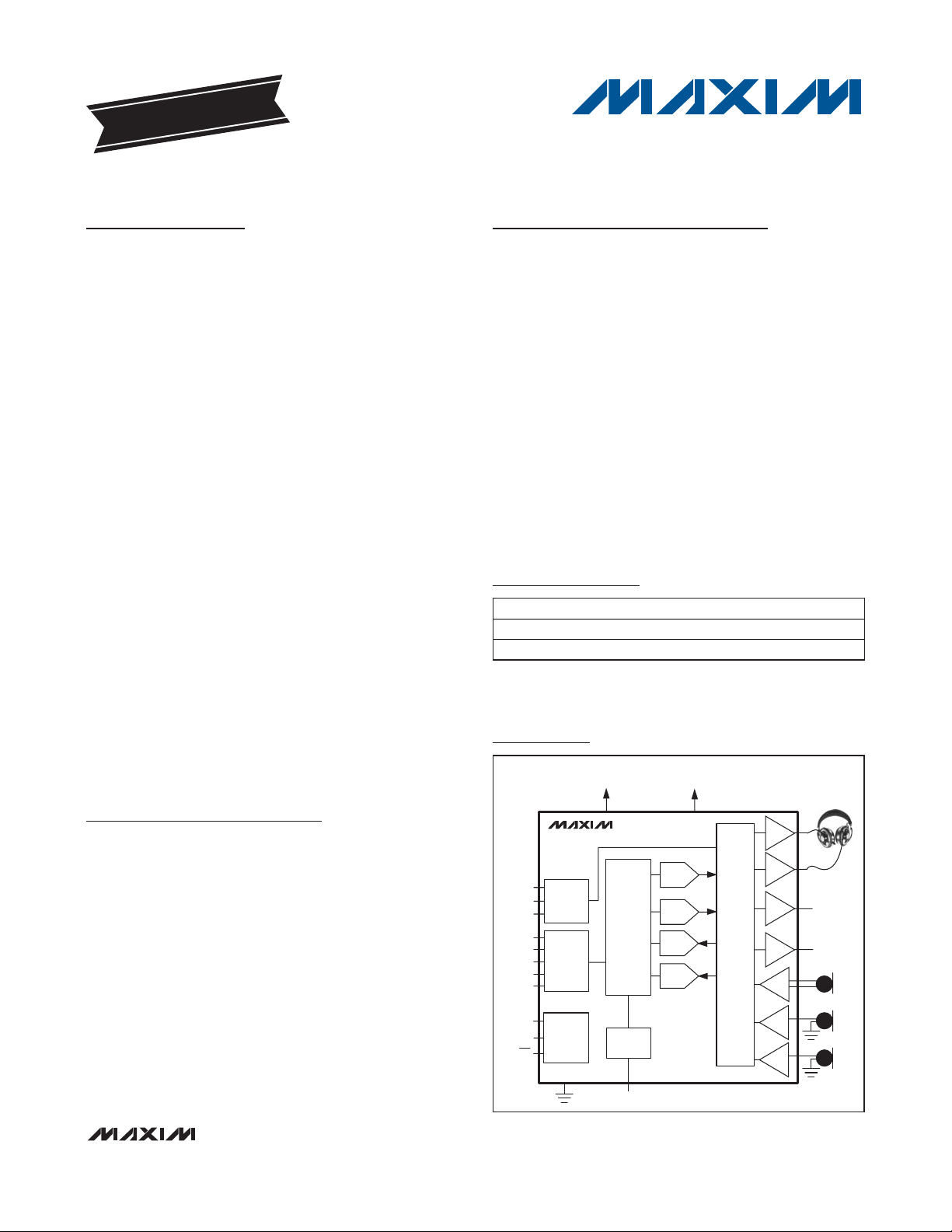
The MAX9856 is a high-performance, low-power stereo
audio CODEC designed for MP3, personal media players (PMPs), or other portable multimedia devices.
Using on-board stereo DirectDrive
®
headphone amplifiers, the CODEC can output 30mW into stereo 32Ω
headphones while operating from a single 1.8V power
supply. Very low 9mW playback power consumption
makes it an ideal choice for battery-powered applications. The MAX9856 provides microphone input amplifiers, plus flexible input selection, signal mixing, and
automatic gain control (AGC). Comprehensive loadimpedance sensing allows the MAX9856 to autodetect
most common audio and audio/video headset and jack
plug types.
Outputs include stereo DirectDrive line outputs and
DirectDrive headphone amplifiers. The stereo ADC can
convert audio signals from either internal or external
microphones that can be configured for single-ended
or differential signal inputs. Line inputs can be configured as stereo, differential, or mono and fed through
one channel of the microphone path. The analog inputs
selected can be gain ranged or mixed with other input
sources prior to conversion to digital. The ADC path
also features programmable digital highpass filters to
remove DC offset voltages and wind noise.
The MAX9856 supports all common sample rates from
8kHz to 48kHz in both master and slave mode. The serial digital audio interfaces support a variety of formats
including I
2
S, left-justified, and PCM modes.
The MAX9856 uses a thermally efficient, space-saving
40-pin, 6mm x 6mm x 0.8mm TQFN package.
Applications
MP3 Players
Personal Media Players
Handheld Gaming Consoles
Cellular Phones
Features
o 1.71V to 3.6V Single-Supply Operation
o Stereo 30mW DirectDrive Headphone Amplifier
o Stereo 1V
RMS
DirectDrive Line Outputs
(V
DD
= 1.8V) and Stereo Line Inputs
o Low-Noise Stereo and Mono Differential
Microphone Inputs with Automatic Gain Control
and Noise Quieting
o 9mW Playback Power Consumption (V
DD
= 1.8V)
o 91dB 96kHz 18-Bit Stereo DAC
o 85dB 48kHz 18-Bit Stereo ADC
o Supports Any Master Clock Frequency from
10MHz to 60MHz
o ADCs and DACs Can Run at Independent Sample
Rates
o Flexible Audio Mixing and Volume Control
o Clickless/Popless Operation
o Headset Detection Logic
o I
2
C Control Interface
MAX9856
Low-Power Audio CODEC with
DirectDrive Headphone Amplifiers
________________________________________________________________
Maxim Integrated Products
1
Ordering Information
Simplified Block Diagram
19-1288; Rev 2; 12/11
For pricing, delivery, and ordering information, please contact Maxim Direct at 1-888-629-4642,
or visit Maxim’s website at www.maxim-ic.com.
EVALUATION KIT
AVAILABLE
+
Denotes a lead-free/RoHS-compliant package.
*
EP = Exposed pad.
/V denotes an automotive qualified part.
Pin Configuration appears at end of data sheet.
DirectDrive is a registered trademark of Maxim Integrated
Products, Inc.
PART TEMP RANGE PIN-PACKAGE
MAX9856ETL+ -40°C to +85°C 40 TQFN-EP*
MAX9856GTL/V+ -40°C to +105°C 40 TQFN-EP*
AND DVDDS2
DVDD
1.71V TO 3.6V
AVDD AND CPVDD
1.71V TO 3.6V
MAX9856
AUXIN
LINEIN1
LINEIN2
SDOUT
SDIN
BCLK
LRCLK_D
LRCLK_A
SDA
SCL
MUX
DIGITAL
INTERFACE
2
C
I
IRQ
DIGITAL
FILTERING
AND
MIXERS
CLOCK
CONTROL
MCLK
DAC
DAC
ADC
ADC
ANALOG
MIXERS
LEFT LINE
OUT
RIGHT LINE
OUT
DIFF
MIC
LEFT
EXT
MIC
RIGHT
EXT
MIC
Page 2
MAX9856
Low-Power Audio CODEC with
DirectDrive Headphone Amplifiers
2 _______________________________________________________________________________________
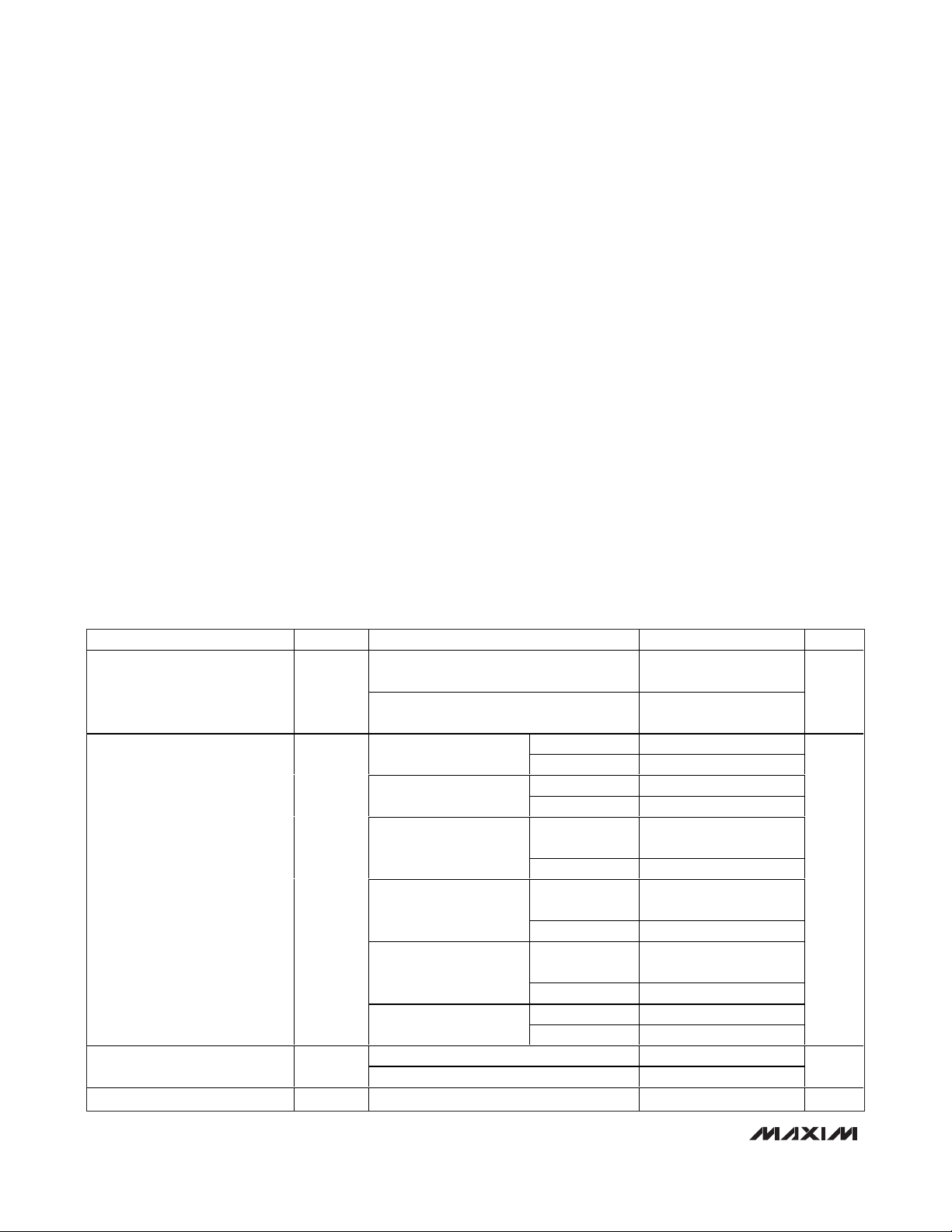
ABSOLUTE MAXIMUM RATINGS
ELECTRICAL CHARACTERISTICS
(V
AVDD
= V
CPV
DD
= V
DV
DDS2
= V
DV
DD
= 1.8V, RHP= 32Ω, R
LINE
= 10kΩ, C1 = 4.7µF, C2 = 4.7µF, C
REF
= C
MBIAS
= C
PREG
=
C
NREG
= 1µF, A
V
PRE
= +20dB, C
MICBIAS
= 1µF, A
VMIGPGA
= 0dB, f
MCLK
= 11.2896MHz, DRATE = 00, TA= T
MIN
to T
MAX
, unless
otherwise noted. Typical values are at T
A
= +25°C.) (Note 1)
Stresses beyond those listed under “Absolute Maximum Ratings” may cause permanent damage to the device. These are stress ratings only, and functional
operation of the device at these or any other conditions beyond those indicated in the operational sections of the specifications is not implied. Exposure to
absolute maximum rating conditions for extended periods may affect device reliability.
(Voltages with respect to AGND.)
AVDD, DVDD, DVDDS2, CPVDD .............................-0.3V to +4V
PVSS, SVSS........................................Capacitor connection only
AGND, DGND, CPGND.........................................-0.3V to +0.3V
HPL, HPR .................................(V
SVSS
- 0.3V) to (V
AVDD
+ 0.3V)
HGNDSNS, LGNDSNS, MICGND .........................-0.3V to +0.3V
JACKSNS .................................(V
SVSS
- 0.3V) to (V
AVDD
+ 0.3V)
LOUTL, LOUTR ........................(V
SVSS
- 0.3V) to (V
AVDD
+ 0.3V)
LINEIN1, LINEIN2, AUXIN ...........................................-2V to +2V
MICL, MICR, INLP, INLM, INRM..................................-2V to +2V
C1N........................................(V
PVSS
- 0.3V) to (V
CPGND
+ 0.3V)
C1P .....................................(V
CPGND
- 0.3V) to (V
CPVDD
+ 0.3V)
PREG, REF, MBIAS, MICBIAS................-0.3V to (V
AVDD
+ 0.3V)
NREG ......................................................(V
SVSS
- 0.3V) to +0.3V
MCLK........................................................................-0.3V to +4V
SDA, SCL, IRQ .........................................................-0.3V to +4V
LRCLK_A, LRCLK_D, BCLK,
SDIN, SDOUT ..................................-0.3V to (V
DVDDS2
+ 0.3V)
Continuous Current Into/Out of HPR/HPL/
LOUTL/LOUTR ...............................................................150mA
CPVDD/CPGND/C1P/C1N/PVSS ......................................300mA
Any Other Pin ......................................................................20mA
Duration of HPR/HPL/LOUTL/LOUTR Short Circuit
to AVDD/AGND/CPVDD/CPGND ............................Continuous
Continuous Power Dissipation (T
A
= +70°C)
40-Pin TQFN (derate 26.3mW/°C above +70°C,
single-layer board) ......................................................2105mW
40-Pin TQFN (derate 37mW/°C above +70°C,
multilayer board) .........................................................2963mW
Operating Temperature Ranges:
E Series.............................................................-40°C to +85°C
G Series ..........................................................-40°C to +105°C
Storage Temperature Range .............................-65°C to +150°C
Lead Temperature (soldering, 10s) .................................+300°C
Soldering Temperature (reflow) .......................................+260°C
PARAMETER SYMBOL CONDITIONS MIN TYP MAX UNITS
AVDD = CPVDD (inferred from HP output
Supply Voltage Range
PSRR)
DVDD, DVDDS2 (inferred from CODEC
performance tests)
DAC playback mode
(f
= 44.1kHz) analog
S
Line-only playback mode
(DAC/ADC disabled)
DAC + line input
playback mode
(f
= 44.1kHz)
S
Total Supply Current (Note 2) I
VDD
Full operation, fS =
44.1kHz (DAC + ADC +
LINEIN + MIC + AUXIN)
DAC playback, fS =
44.1kHz mono ADC
record f
= 8kHz
S
ADC record,
f
= 44.1kHz
S
I
+ I
Shutdown Supply Current
AVDD
I
DVDD
+ I
CPVDD
DVDDS2
Shutdown to Full Operation 50 ms
1.71 1.80 3.60
1.71 1.80 3.60
I
AVDD
I
DVDD
I
AVDD
I
DVDD
I
AVDD
I
DVDD
I
AVDD
I
DVDD
I
AVDD
I
DVDD
I
AVDD
I
DVDD
+ I
+ I
+ I
+ I
+ I
+ I
+ I
+ I
+ I
+ I
+ I
+ I
CPVDD
DVDDS2
CPVDD
DVDDS2
CPVDD
DVDDS2
CPVDD
DVDDS2
CPVDD
DVDDS2
CPVDD
DVDDS2
2.9 5.1
2.3
2.9 4.3
0.14 0.20
3.9 5.4
2.3 3.5
11.0 15.5
3.7 4.5
6.6 9.1
2.8 3.5
7.8 10.5
2.3 3.5
2.2 10
0.6 10
V
mA
µA
Page 3
MAX9856
Low-Power Audio CODEC with
DirectDrive Headphone Amplifiers
_______________________________________________________________________________________ 3
ELECTRICAL CHARACTERISTICS (continued)
(V
AVDD
= V
CPV
DD
= V
DV
DDS2
= V
DV
DD
= 1.8V, RHP= 32Ω, R
LINE
= 10kΩ, C1 = 4.7µF, C2 = 4.7µF, C
REF
= C
MBIAS
= C
PREG
=
C
NREG
= 1µF, A
V
PRE
= +20dB, C
MICBIAS
= 1µF, A
VMIGPGA
= 0dB, f
MCLK
= 11.2896MHz, DRATE = 00, TA= T
MIN
to T
MAX
, unless
otherwise noted. Typical values are at T
A
= +25°C.) (Note 1)
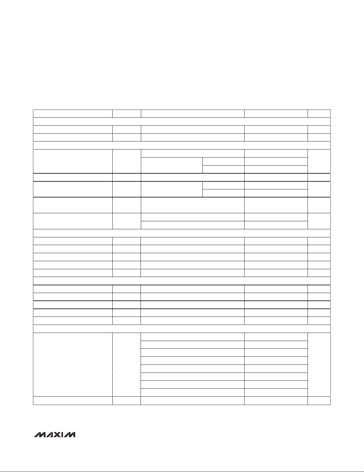
PARAMETER SYMBOL CONDITIONS MIN TYP MAX UNITS
STEREO DAC (Note 3)
Gain Error ±1 ±5 %
Channel Gain Mismatch ±1 %
DAC DYNAMIC SPECIFICATIONS
fS = 44.1kHz, A-weighted, DRATE = 10 80 91
Dynamic Range (Note 4)
= 8kHz to 96kHz,
f
S
A-weighted
DRATE = 00 87
DRATE =10 91
Total Harmonic Distortion THD fIN = 1kHz, fS = 8kHz to 96kHz, 0dBFS 82 dB
Signal-to-Noise Ratio SNR
Crosstalk
Power-Supply Rejection Ratio PSRR
f
= 8kHz to 96kHz,
S
A-weighted (Note 5)
Driven channel at -1dBFS, f
= 8kHz
f
S
f = 217Hz, V
f = 10kHz, V
RIPPLE
RIPPLE
= 100mV, A
= 100mV, A
DRATE = 00 87
DRATE = 10 91
= 1kHz,
IN
= 0dB 93
VPGA
= 0dB 60
VPGA
78 dB
DAC DIGITAL FILTER (8x interpolation, FIR (fS = 7.8kHz to 50kHz))
Passband Cutoff f
Passband Ripple f < 0.44 x f
Stopband Cutoff f
Stopband Attenuation f > f
-0.2dB from peak 0.44 f
P
S
S
S
±0.1 dB
0.58 f
58 dB
Attenuation at fS/2 -6.02 dB
DAC DIGITAL FILTER (4x interpolation, FIR (fS = 50kHz to 100kHz))
Passband Cutoff f
Passband Ripple f < 0.23 x f
Stopband Cutoff f
Stopband Attenuation f > f
-0.2dB from peak 0.24 f
P
S
S
S
±0.1 dB
0.5 f
54 dB
Attenuation at fS/2 -60 dB
DAC HIGHPASS FILTER
DACHP = 000 Disabled
DACHP = 001; LRCLK/1598 28
DACHP = 010; LRCLK/798 55
-3dB Corner Frequency
= 44.1kHz)
(f
S
HP
DACHP = 011; LRCLK/398 111
FILT
DACHP = 100; LRCLK/197 224
DACHP = 101; LRCLK/97 455
DACHP = 110; LRCLK/47 938
DACHP = 111; LRCLK/22 2004
DC Attenuation DC
ATTEN
DACHP ≠ 000 60 dB
dB
dB
dB
S
S
S
S
Hz
Page 4
MAX9856
Low-Power Audio CODEC with
DirectDrive Headphone Amplifiers
4 _______________________________________________________________________________________
ELECTRICAL CHARACTERISTICS (continued)
(V
AVDD
= V
CPV
DD
= V
DV
DDS2
= V
DV
DD
= 1.8V, RHP= 32Ω, R
LINE
= 10kΩ, C1 = 4.7µF, C2 = 4.7µF, C
REF
= C
MBIAS
= C
PREG
=
C
NREG
= 1µF, A
V
PRE
= +20dB, C
MICBIAS
= 1µF, A
VMIGPGA
= 0dB, f
MCLK
= 11.2896MHz, DRATE = 00, TA= T
MIN
to T
MAX
, unless
otherwise noted. Typical values are at T
A
= +25°C.) (Note 1)
PARAMETER SYMBOL CONDITIONS MIN TYP MAX UNITS
STEREO ADC (Note 6)
Gain Error ±1 ±5 %
Full-Scale Conversion 0dBFS fIN = 1kHZ, line input PGA = 0dB 2 V
Channel Gain Mismatch ±1 %
ADC DYNAMIC SPECIFICATIONS
fS = 8kHz to 32kHz, BW = 22Hz to fS/2 80
Dynamic Range (Note 4)
Total Harmonic Distortion THD
fS = 44.1kHz, BW = 22Hz to 20kHz,
A-weighted
f
= 48kHz, BW = 22Hz to 20kHz,
S
A-weighted
1kHz, 0dBFS, fS = 8kHz -63
1kHz, 0dBFS, f
= 48kHz -68
S
1kHz, 0dBFS, fS = 8kHz, BW = 22Hz to
20kHz, A-weighted
78 84
85
77
Signal-to-Noise Ratio SNR
Channel Crosstalk
Power-Supply Rejection Ratio
(Note 7)
PSRR
1kHz, 0dBFS, f
20kHz, A-weighted
Driven channel at -1dBFS, f
= 8kHz
f
S
V
= 1.71V to 3.6V 60 100
AVDD
f = 1kHz, V
f = 10kHz, V
= 48kHz, BW = 22Hz to
S
= 1kHz,
IN
= 100mV 80
RIPPLE
= 100mV 50
RIPPLE
77
65 dB
ADC DIGITAL FILTER PATH
Passband Cutoff f
Passband Ripple f < f
Stopband Cutoff f
Stopband Attenuation f > f
-0.2dB from peak 0.44 f
P
P
S
S
±0.1 dB
0.56 f
60 dB
Attenuation at fS/2 -6.02 dB
ADC HIGHPASS FILTER
ADCHP = 000 Disabled
ADCHP = 001; LRCLK/1598 28
ADCHP = 010; LRCLK/798 55
-3dB Corner Frequency
(f
= 44.1kHz)
S
HP
FILT
ADCHP = 011; LRCLK/398 111
ADCHP = 100; LRCLK/197 224
ADCHP = 101; LRCLK/97 455
ADCHP = 110; LRCLK/47 938
ADCHP = 111; LRCLK/22 2004
DC Attenuation DC
ATTEN
ADCHP anything other than 000 90 dB
DC Output Offset ADCHP = 000 -40 dBFS
P-P
dB
dB
dB
dB
S
S
Hz
Page 5
MAX9856
Low-Power Audio CODEC with
DirectDrive Headphone Amplifiers
_______________________________________________________________________________________ 5
ELECTRICAL CHARACTERISTICS (continued)
(V
AVDD
= V
CPV
DD
= V
DV
DDS2
= V
DV
DD
= 1.8V, RHP= 32Ω, R
LINE
= 10kΩ, C1 = 4.7µF, C2 = 4.7µF, C
REF
= C
MBIAS
= C
PREG
=
C
NREG
= 1µF, A
V
PRE
= +20dB, C
MICBIAS
= 1µF, A
VMIGPGA
= 0dB, f
MCLK
= 11.2896MHz, DRATE = 00, TA= T
MIN
to T
MAX
, unless
otherwise noted. Typical values are at T
A
= +25°C.) (Note 1)
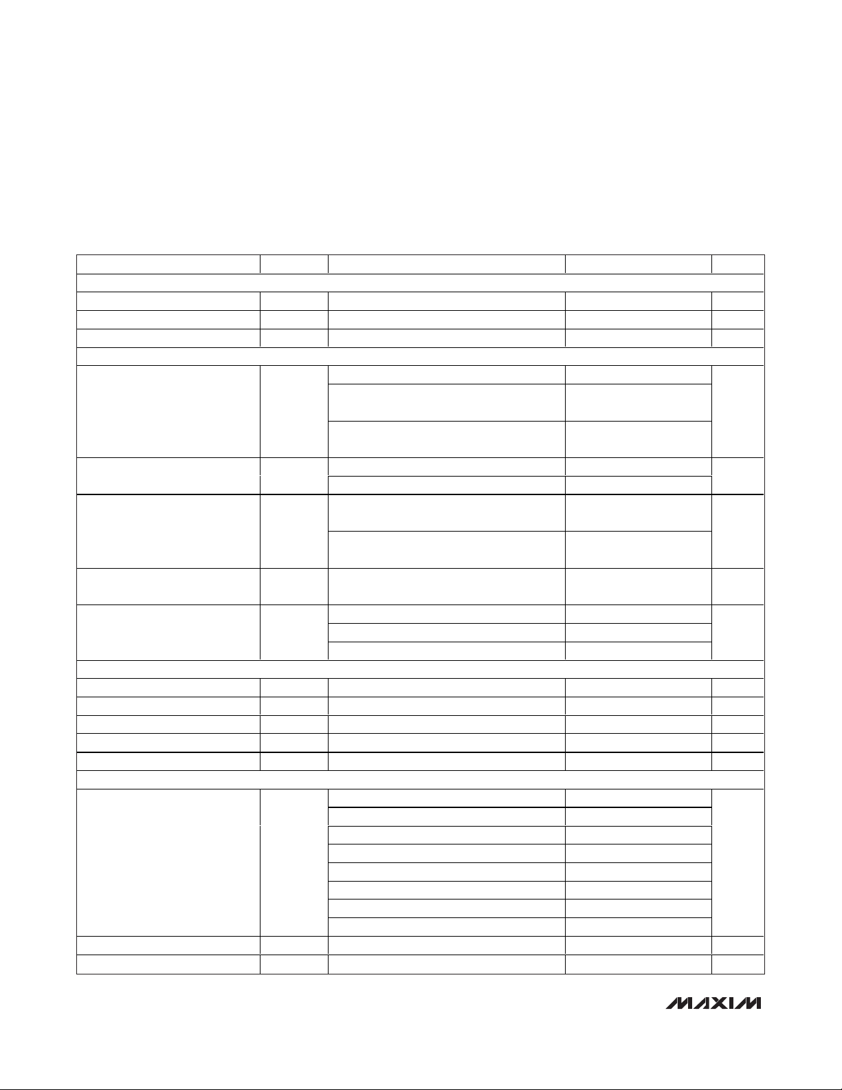
PARAMETER SYMBOL CONDITIONS MIN TYP MAX UNITS
ADC/DAC DATA RATE ACCURACY
LRCLK_D and LRCLK_A Output
Average Sample Rate Deviation
(Note 8) -0.025 +0.025 %
(Master Mode, Any MCLK)
LRCLK_D Output Sample Rate
Deviation (Master Mode)
LRCLK Input Sample Rate Range
(Slave Mode)
LRCLK_D and LRCLK_A PLL
Lock Time
LRCLK_D and LRCLK_A
Acceptable Jitter for Maintaining
PLL Lock (All Slave Modes)
t
LOCK
PCLK/LRCLK = 1536, 1024, 768, 512, 384,
256, 192, or 128
0%
LRCLK_A, LRCLK_D (DHF = 0) 7.8 50
LRCLK_D (DHF = 1) 15.6 100
Any allowable LRCLK and PCLK rates 12 25 ms
Allowable LRCLK period change from
nominal for slave PLL mode at any
±20 ns
allowable LRCLK and PCLK rates
HEADPHONE AMPLIFIERS
Output Power P
OUT
f = 1kHz, THD < 1%,
= +25°C
T
A
RL = 16Ω 35
R
= 32Ω 15 28
L
0dBFS DAC Output Voltage +0dB volume setting 3.40 3.51 3.80 V
Line In to HP Out Voltage Gain +4.5dB volume setting, 0dB PGA setting 1.77 V/V
Output Offset Voltage V
Total Harmonic Distortion Plus
Noise
OS
THD+N
Dynamic Range DR
Capacitive Drive C
Crosstalk
Channel Gain Matching A
VMATCH
Click-and-Pop Level
TA = +25°C, -40dB volume setting ±0.6 ±4 mV
RL = 32Ω, P
= 16Ω, P
R
L
+5.5dB volume setting, DAC input at
= 44.1kHz (Note 4)
f
S
V
= 1.71V to 3.6V 70 94
AVDD
V
= 100mV
RIPPLE
V
= 100mV
RIPPLE
No sustained oscillations 150 pF
L
= 1.6mW, f = 1kHz, (HPL to HPR) or
P
OUT
(HPR to HPL)
= 25mW, f = 1kHz 0.03
OUT
= 25mW, f = 1kHz 0.05
OUT
80 91 dB
, f = 217Hz 80Power-Supply Rejection Ratio PSRR
P-P
, f = 10kHz 50
P-P
69 dB
±2 %
Peak voltage,
A-weighted, 32 samples
per second
Into shutdown -70
Out of shutdown -70
LINE AMPLIFIERS
0dBFS DAC Output Voltage 1.0 V
Line-In to Line-Out Voltage Gain 0dB input PGA setting 1.3 1.34 1.4 V/V
Output Offset Voltage V
OS
TA = +25°C ±0.7 ±10 mV
kHz
mW
P-P
%
dB
dBV
RMS
Page 6
MAX9856
Low-Power Audio CODEC with
DirectDrive Headphone Amplifiers
6 _______________________________________________________________________________________
ELECTRICAL CHARACTERISTICS (continued)
(V
AVDD
= V
CPV
DD
= V
DV
DDS2
= V
DV
DD
= 1.8V, RHP= 32Ω, R
LINE
= 10kΩ, C1 = 4.7µF, C2 = 4.7µF, C
REF
= C
MBIAS
= C
PREG
=
C
NREG
= 1µF, A
V
PRE
= +20dB, C
MICBIAS
= 1µF, A
VMIGPGA
= 0dB, f
MCLK
= 11.2896MHz, DRATE = 00, TA= T
MIN
to T
MAX
, unless
otherwise noted. Typical values are at T
A
= +25°C.) (Note 1)
Total Harmonic Distortion Plus
Noise
PARAMETER SYMBOL CONDITIONS MIN TYP MAX UNITS
THD+N V
= 1V
OUT
, f = 1kHz 0.024 %
RMS
Signal-to-Noise Ratio SNR 98 dB
V
= 1.71V to 3.6V 70 108
AVDD
dB
Capacitive Drive C
Crosstalk
Channel Gain Matching A
VMATCH
V
= 100mV
RIPPLE
= 100mV
V
RIPPLE
No sustained oscillations 150 pF
L
V
= 2V
OUT
P-P
or (LOUTR to LOUTL)
, f = 217Hz 93Power-Supply Rejection Ratio PSRR
P-P
, f = 10kHz 60
P-P
, f = 1kHz, (LOUTL to LOUTR)
98 dB
±2 %
VOLUME CONTROL
Headphone Volume Control
Range
-74.0 +5.5 dB
5.5dB to 2dB 0.5
Headphone Volume Control Step
Size
+2.5dB to -2dB 1
-2dB to -46dB 2
dB
-46dB to -74dB 4
Headphone Mute Attenuation f = 1kHz 92 dB
CHARGE PUMP
Charge-Pump Oscillator
Frequency
f
OSC
TA = +25°C 600 665 720 kHz
MICROPHONE AMPLIFIERS
PALEN/PAREN = 01 -0.5 0 +0.5
Preamplifier Gain A
VPRE
MICL or MICR
PALEN/PAREN = 10 19 20 21
dB
PALEN/PAREN = 11 28.5 30.0 31.5
MIC PGA Gain A
VMICPGA
PGAML/R = 0x20 -0.5 0 +0.5
PGAML/R = 0x00 19.5 20.0 19.5
dB
MIC PGA Gain Step Size 1dB
MIC Mute Attenuation f = 1kHz 92 dB
INL±, V
Common-Mode Rejection Ratio CMRR
A
VPRE
IN
= +20dB
INL±, MICL or MICR, A
MIC Input Resistance R
IN_MIC
INL±, MICL or MICR, A
INL±, MICL or MICR, A
MIC Input Resistance Matching R
MIC Input Bias Voltage V
MATCH
CML
INL+ to INL- or MICL/MICR to AGND 1 %
Measured at INL±, MICR, MICL, and AGND -0.05 0 +0.05 V
Input Voltage Noise f = 1kHz, A
= 100mV
VPRE
at 217Hz,
P-P
= +30dB 4 8 10
VPRE
= +20dB 12 18 28
VPRE
= 0dB 60 100 160
VPRE
73 dB
kΩ
= +30dB 15 nV/√Hz
Page 7
MAX9856
Low-Power Audio CODEC with
DirectDrive Headphone Amplifiers
_______________________________________________________________________________________ 7
ELECTRICAL CHARACTERISTICS (continued)
(V
AVDD
= V
CPV
DD
= V
DV
DDS2
= V
DV
DD
= 1.8V, RHP= 32Ω, R
LINE
= 10kΩ, C1 = 4.7µF, C2 = 4.7µF, C
REF
= C
MBIAS
= C
PREG
=
C
NREG
= 1µF, A
V
PRE
= +20dB, C
MICBIAS
= 1µF, A
VMIGPGA
= 0dB, f
MCLK
= 11.2896MHz, DRATE = 00, TA= T
MIN
to T
MAX
, unless
otherwise noted. Typical values are at T
A
= +25°C.) (Note 1)
Total Harmonic Distortion Plus
Noise
MIC Power-Supply Rejection
Ratio
PARAMETER SYMBOL CONDITIONS MIN TYP MAX UNITS
THD+N
PSRR
A
VPRE
V
IN
A
VPRE
V
IN
A
VPRE
V
IN
V
AVDD
V
RIPPLE
V
RIPPLE
= 0dB, A
= 500mV
VMICPGA
, f = 1kHz, A-weighted
P-P
= +20dB, A
= 50mV
, f = 1kHz, A-weighted
P-P
= +30dB, A
= 18mV
, f = 1kHz, A-weighted
P-P
=1.71V to 3.6V, TA = +25°C 79 80
= 100mV at 1kHz, input referred 80
= 100mV at 10kHz, input referred 50
= 0dB,
VMICPGA
VMICPGA
= 0dB,
= 0dB,
0.04
0.08
0.08
MICROPHONE BIAS
V
= 1.8V (MBSEL = 0 register setting) 1.4 1.5 1.6
MICBIAS Output Voltage V
MICBIAS
MICBIAS Load Regulation I
AVDD
V
= 3.0V (MBSEL = 1 register setting) 2.3 2.4 2.5
AVDD
= 0 to 2mA 0.8 10 Ω
MICBIAS
MICBIAS Capacitive Load Minimum capacitive load 1 µF
MICBIAS Short-Circuit Current To GND 14 mA
V
= 1.71V to 3.6V, MBSEL = 0,
MICBIAS Power-Supply Rejection
Ratio
MICBIAS Noise Voltage
PSRR
V
NOISEMIC
BIAS
AVDD
= +25°C
T
A
V
= 100mV at 1kHz 86
RIPPLE
= 100mV at 10kHz 76
V
RIPPLE
MBSET = 0 or 1
f = 10Hz to 20kHz 3 µV
f = 1kHz 20 nV/√Hz
75 86
AUTOMATIC GAIN CONTROL
Threshold Level Set by AGCSTH[3:0] -3 -18 dB
Attack Time Set by AGCATK[1:0] 3 200 ms
Release Time Set by AGCRLS[2:0] 0.078 10.000 s
Hold Time Set by AGCHLD[1:0] 50 400 ms
A
= +30dB 30 to 50
VPRE
A
= +20dB 20 to 40Gain Adjustment Range
VPRE
= 0dB 0 to 20
A
VPRE
ADC LOW-LEVEL QUIETING
Full 12dB quieting at 1dB of
attenuation/(gain) for every 2dB
NG Attack and Release Time
decrease/(increase) of signal level
0.5 s
(immediate release if PGA < 20dB gain
when AGC is enabled)
ANTH[3:0] setting range (AGC off) (AGC on
NG Threshold Level
adjusts these values by 20dB since lowlevel signals cause maximum AGC gain in
-64 -28 dB
the PGA)
NG Attenuation
1dB of attenuation for every 2dB signal
amplitude decrease from NG threshold
012dB
%
dB
V
dB
RMS
dB
Page 8
MAX9856
Low-Power Audio CODEC with
DirectDrive Headphone Amplifiers
8 _______________________________________________________________________________________
ELECTRICAL CHARACTERISTICS (continued)
(V
AVDD
= V
CPV
DD
= V
DV
DDS2
= V
DV
DD
= 1.8V, RHP= 32Ω, R
LINE
= 10kΩ, C1 = 4.7µF, C2 = 4.7µF, C
REF
= C
MBIAS
= C
PREG
=
C
NREG
= 1µF, A
V
PRE
= +20dB, C
MICBIAS
= 1µF, A
VMIGPGA
= 0dB, f
MCLK
= 11.2896MHz, DRATE = 00, TA= T
MIN
to T
MAX
, unless
otherwise noted. Typical values are at T
A
= +25°C.) (Note 1)
PARAMETER SYMBOL CONDITIONS MIN TYP MAX UNITS
LINEIN1/LINEIN2 INPUTS
Line Input Full-Scale Input
Voltage
0dBFS 2 V
P-P
Input DC Bias Voltage 0V
Line Input Resistance R
Crosstalk
Line Channel-to-Channel Gain
Matching
AV
MATCH
PGA = 0dB (Note 9) 12 21 kΩ
IN
LINEIN1 to LINEIN2 or LINEIN2 to
LINEIN1, f = 1kHz
97 dB
±2 %
PGA Gain Range -32 +30 dB
PGA Gain Step Size -32dB to +30dB 2 dB
AUXIN INPUT
AUXIN Full-Scale Input Voltage 0dBFS AUXDC = 0 2 V
P-P
Input DC Voltage Range AUXDC = 1 0 1 V
Input DC Bias Voltage AUXDC = 0 0 V
AUXIN Input Resistance R
Line Channel-to-Channel Gain
Matching
AV
MATCH
AUXDC = 0 12 21 kΩ
IN
AUXDC = 1 100 MΩ
±2 %
PGA Gain Range -32 +30 dB
PGA Gain Step Size -32dB to +30dB 2 dB
JACK SENSE OPERATION (EN[2:0] = 000)
JACKSNS High Threshold
(JKMIC)
JACKSNS Deglitch Period
(JKMIC)
V
TH1
t
GLITCH
TA = +25°C
Pulses shorter than t
are eliminated 12 ms
GLITCH
JACKSNS Voltage (JKMIC) JDETEN = 1 V
0.92 x
V
MICBIAS
0.95 x
V
MICBIAS
AV DD
0.98 x
V
MICBIAS
V
V
HEADSET IMPEDANCE DETECT MODE (EN[2:0] = 111)
JACKSNS/HPL/HPR High
Threshold
V
TH2
HPL/HPR disabled 0.32 0.40 0.48 V
(JSDET/ HSDETL/HSDETR)
JACKSNS/HPL/HPR Low
Threshold
V
TH3
HPL/HPR disabled 0.075 0.100 0.125 V
(JSDET/HSDETL/HSDETR)
JACKSNS/HPL/HPR Sense
Current
I
SNS
HPL/HPR disabled 1.7 2.0 2.3 mA
(JSDET/HSDETL/HSDETR)
Page 9
MAX9856
Low-Power Audio CODEC with
DirectDrive Headphone Amplifiers
_______________________________________________________________________________________ 9
DIGITAL INTERFACE ELECTRICAL CHARACTERISTICS
(V
DVDD
= V
DVDDS2
= 1.8V, TA= T
MIN
to T
MAX
, unless otherwise noted.) (Note 1)
ELECTRICAL CHARACTERISTICS (continued)
(V
AVDD
= V
CPV
DD
= V
DV
DDS2
= V
DV
DD
= 1.8V, RHP= 32Ω, R
LINE
= 10kΩ, C1 = 4.7µF, C2 = 4.7µF, C
REF
= C
MBIAS
= C
PREG
=
C
NREG
= 1µF, A
V
PRE
= +20dB, C
MICBIAS
= 1µF, A
VMICPGA
= 0dB, MCLK = 11.2896MHz, DRATE = 00, TA= T
MIN
to T
MAX
, unless
otherwise noted. Typical values are at T
A
= +25°C.) (Note 1)
PARAMETER SYMBOL CONDITIONS MIN TYP MAX UNITS
SLEEP MODE (JDETEN = 1, SHDNB = 0)
JACKSNS/HPL Resistance R
JACKSNS/HPL Sense Voltage V
JACKSNS/HPL Sleep Threshold
(JKSNS/LSNS)
V
TH4
MICBIAS = GND 400 1000 kΩ
PU
PU
V
AVDD
0.8V
V
AVDD
-
V
-
AVDD
0.4V
V
AVDD
0.15V
V
V
PARAMETER SYMBOL CONDITIONS MIN TYP MAX UNITS
MCLK INPUT CHARACTERISTICS
Input Voltage High V
Input Voltage Low V
Input Leakage Current IIH, I
IH
IL
IL
0.7 x V
DVDD
0.4 V
-10 +10 µA
V
Input Capacitance 3pF
MCLK Input Frequency 10 60 MHz
MCLK Duty Cycle 40 50 60 %
Maximum MCLK Input Jitter For guaranteed performance limits 100 ps
RMS
DIGITAL INPUTS (BCLK, LRCLK_A, LRCLK_D, SDIN, SDA, SCL)
Input Voltage High V
Input Voltage Low V
IH
IL
0.7 x V
DVDD
0.3 x V
DVDD
V
V
Input Hysteresis 200 mV
Input Leakage Current IIH, I
IL
-10 +10 µA
Input Capacitance 10 pF
CMOS DIGITAL OUTPUTS (BCLK, LRCLK_A, LRCLK_D, SDOUT)
Output Low Voltage V
Output High Voltage V
OL
OH
IOL = 3mA 0.4 V
IOH = 3mA V
- 0.4 V
DVDD
OPEN-DRAIN DIGITAL OUTPUTS (IRQ, SDA)
Output High Current I
Output Low Voltage V
OH
OL
V
OUT
= V
DVDD
1µA
IOL = 3mA 0.4 V
DIGITAL AUDIO INTERFACE TIMING CHARACTERISTICS
BCLK Cycle Time
BCLK High Time t
BCLK Low Time t
BCLK or LRCLK_A/D Rise and
Fall Time
t
BCLKS
t
BCLKM
BCLKH
BCLKL
t
r , tf
Slave operation 75 ns
Master operation 100 325 ns
Slave operation 30 ns
Master operation 30 ns
Master operation, CL = 15pF 7 ns
Page 10
MAX9856
Low-Power Audio CODEC with
DirectDrive Headphone Amplifiers
10 ______________________________________________________________________________________
Note 1: All devices are 100% production tested at room temperature. All temperature limits are guaranteed by design.
Note 2: Supply current measurements taken with no applied input signal to line and microphone inputs. A digital zero audio signal
used for all digital serial audio inputs. Speaker and headphone outputs are loaded as stated in the global conditions.
Note 3: DAC performance measured at headphone outputs.
Note 4: Dynamic range measured using the EIAJ method. The input is applied at -60dBFS, f
IN
= 1kHz. The is THD+N referred to
0dBFS.
Note 5: Signal-to-noise ratio measured using an all-zeros input signal, and is relative to 0dB full scale. The DAC is not muted for the
SNR measurement.
Note 6: Performance measured from line inputs (unless otherwise noted).
Note 7: Microphone amplifiers connected to ADC, microphone inputs AC-grounded.
Note 8: In master-mode operation, the accuracy of the MCLK input proportionally determines the accuracy of the sample clock
rate. (V
DVDD
= 1.8V, unless otherwise noted).
Note 9: To enable the line input, make sure the desired input is selected by either the audio output mixer or the ADC input mixer.
Note 10: C
B
is in pF.
DIGITAL INTERFACE ELECTRICAL CHARACTERISTICS (continued)
(V
DVDD
= V
DVDDS2
= 1.8V, TA= T
MIN
to T
MAX
, unless otherwise noted.) (Note 1)
SDIN or LRCLK_A/D to BCLK
Rising Setup Time
SDIN or LRCLK_A/D to BCLK
Rising Hold Time
SDOUT Delay Time t
I2C INTERFACE TIMING CHARACTERISTICS
Serial-Clock Frequency f
Bus Free Time Between STOP
and START Conditions
Hold Time (Repeated) START
Condition
SCL Pulse Width Low t
SCL Pulse Width High t
Setup Time for a Repeated
START Condition
Data Hold Time t
Data Setup Time t
SDA and SCL Receiving Rise
Time
SDA and SCL Receiving Fall
Time
SDA Transmitting Fall Time t
Setup Time for STOP Condition t
Bus Capacitance C
Pulse Width of Suppressed Spike t
PARAMETER SYMBOL CONDITIONS MIN TYP MAX UNITS
t
SU
t
HD
DLY
SCL
t
BUF
t
HD,STA
LOW
HIGH
t
SU,STA
HD,DAT
SU,DAT
t
r
t
f
f
SU,STO
b
SP
BCI = 0 (see the I2C Register Address Map
and Definitions section)
BCI = 0 (see the I2C Register Address Map
and Definitions section)
BCI = 0 (see the I2C Register Address Map
and Definitions section), C
(Note 10) 20 + 0.1C
(Note 10) 20 + 0.1C
V
= 1.8V (Note 10) 20 + 0.1C
DVDD
V
= 3.6V (Note 10) 20 + 0.05C
DVDD
TA = +25°C 0 50 ns
= 30pF
L
30 ns
5ns
050ns
0 400 kHz
1.3 µs
0.6 µs
1.3 µs
0.6 µs
0.6 µs
0 900 ns
100 ns
B
B
B
B
0.6 µs
300 ns
300 ns
250
250
400 pF
ns
Page 11
MAX9856
Low-Power Audio CODEC with
DirectDrive Headphone Amplifiers
______________________________________________________________________________________ 11
3
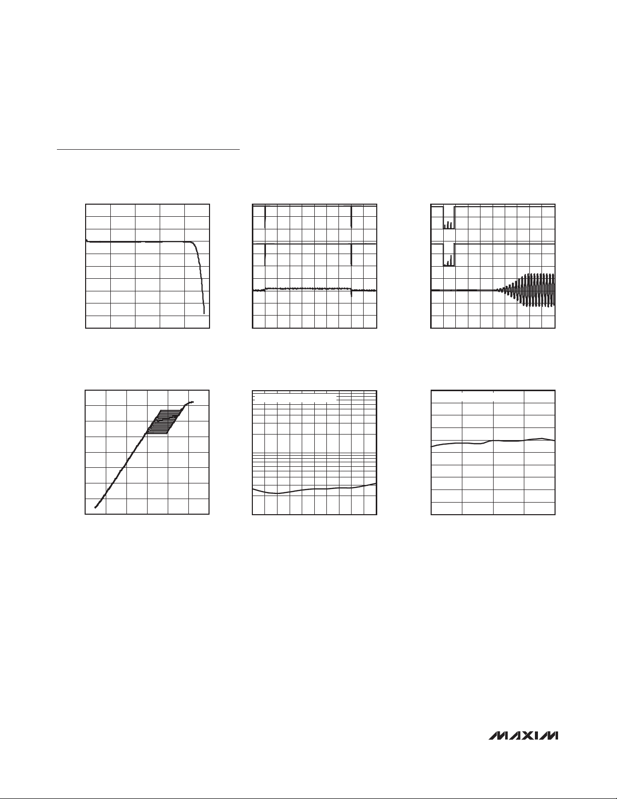
Typical Operating Characteristics
(V
AVDD
= V
CPVDD
= V
DVDDS2
= V
DVDD
= 1.8V, RHP= 32Ω, R
LINE
= 10kΩ, C1 = 4.7µF, C2 = 4.7µF, C
REF
= C
MBIAS
= C
PREG
= C
NREG
=1µF, V
AVPRE
= +20dB, C
MICBIAS
= 1µF, V
AV
MICPGA
= 0dB, f
MCLK
= 12.288MHz, DRATE = 10, TA= +25°C, unless otherwise noted.)
TOTAL HARMONIC DISTORTION PLUS NOISE
vs. OUTPUT POWER (DAC TO HP)
100
HP GAIN = +5.5dB
= 32
R
Ω
L
10
1
THD+N (%)
0.1
0.01
0.001
1kHz
040
OUTPUT POWER (mW)
20kHz
TOTAL HARMONIC DISTORTION + NOISE
vs. FREQUENCY (DAC TO HP)
10
HP GAIN = +5.5dB
= 16
R
Ω
L
1
10kHz
MAX9856 toc01
3530252015105
MAX9856 toc04
TOTAL HARMONIC DISTORTION PLUS NOISE
vs. OUTPUT POWER (DAC TO HP)
100
HP GAIN = +5.5dB
= 16
R
L
10
1
THD+N (%)
0.1
0.01
0.001
060
TOTAL HARMONIC DISTORTION + NOISE
vs. FREQUENCY (DAC TO LINE OUT)
10
V
= 2V
OUT
RL = 10k
1
Ω
1kHz
OUTPUT POWER (mW)
P-P
Ω
20Hz
10kHz
5040302010
MAX9856 toc02
MAX9856 toc05
TOTAL HARMONIC DISTORTION + NOISE
vs. FREQUENCY (DAC TO HP)
10
HP GAIN = +5.5dB
= 32
R
Ω
L
1
0.1
THD+N (%)
0.001
5mW
0.01
20mW
10E+0 100E+
FREQUENCY (Hz)
10E+31E+3100E+0
TOTAL HARMONIC DISTORTION PLUS NOISE
vs. FREQUENCY (LINE IN TO ADC)
10
1
MAX9856 toc03
MAX9856 toc06
0.1
THD+N (%)
0.01
0.001
5mW
20mW
10E+0 100E+3
FREQUENCY (Hz)
10E+31E+3100E+0
TOTAL HARMONIC DISTORTION PLUS NOISE
vs. FREQUENCY (INTMIC TO ADC)
10
ADC
= -3dBFS
OUT
MIC PREAMP = +20dB
MIC GAIN = 0dB
1
0.1
THD+N (%)
0.01
0.001
10 100k
FREQUENCY (Hz)
10k1k100
MAX9856 toc07
0.1
THD+N (%)
0.01
0.001
10E+0 100E+3
FREQUENCY (Hz)
10E+31E+3100E+0
TOTAL HARMONIC DISTORTION PLUS NOISE
vs. FREQUENCY (INTMIC TO ADC)
10
ADC
= -3dBFS
OUT
MIC PREAMP = +30dB
MIC GAIN = 0dB
1
0.1
THD+N (%)
0.01
0.001
10 100k
FREQUENCY (Hz)
10k1k100
MAX9856 toc08
0.1
THD+N (%)
0.01
0.001
10 100k
FREQUENCY (Hz)
POWER OUT
vs. HEADPHONE LOAD
100
THD+N = 10%
10
POWER OUT (mW)
1
THD+N = 1%
10010
HEADPHONE LOAD (Ω)
10k1k100
fIN = 1kHz
MAX9856 toc09
10001
Page 12

MAX9856
Low-Power Audio CODEC with
DirectDrive Headphone Amplifiers
12 ______________________________________________________________________________________
)
)
)
)
)
Typical Operating Characteristics (continued)
(V
AVDD
= V
CPVDD
= V
DVDDS2
= V
DVDD
= 1.8V, RHP= 32Ω, R
LINE
= 10kΩ, C1 = 4.7µF, C2 = 4.7µF, C
REF
= C
MBIAS
= C
PREG
= C
NREG
=1µF, V
AVPRE
= +20dB, C
MICBIAS
= 1µF, V
AV
MICPGA
= 0dB, f
MCLK
= 12.288MHz, DRATE = 10, TA= +25°C, unless otherwise noted.)
-20
0
V
POWER-SUPPLY REJECTION RATIO
vs. FREQUENCY (DAC TO HP)
= 100mV
RIPPLE
P-P
POWER-SUPPLY REJECTION RATIO
vs. FREQUENCY (DAC TO LINE OUT)
0
V
RIPPLE
-20
MAX9856 toc10
= 100mV
P-P
-40
-60
PSRR (dB)
-80
-100
-120
10 100k
FREQUENCY (Hz)
FFT, DAC TO LINE OUT, 48kHz
SYNCHRONOUS SLAVE MODE, -60dBFS
20
0
-20
-40
-60
-80
AMPLITUDE (dBFS)
-100
-120
-140
000E+0 4E+3
6E+3
MCLK = 12.288MHz
LRCLK = 48kHz
PCLK/2
8E+3
12E+3
10E+32E+3
FREQUENCY (Hz
14E+3
FFT, DAC TO LINE OUT, 48kHz
ASYNCHRONOUS SLAVE MODE, 0dBFS
20
0
-20
-40
-60
-80
AMPLITUDE (dBFS)
-100
-120
-140
000E+0 4E+3
6E+3
MCLK = 11.2896MHz
LRCLK = 48kHz
PCLK/2
8E+3
12E+3
10E+32E+3
FREQUENCY (Hz
14E+3
10k1k100
16E+3
16E+3
18E+3
18E+3
20E+3
20E+3
PSRR (dB)
MAX9856 toc13
AMPLITUDE (dBFS)
MAX9856 toc16
AMPLITUDE (dBFS)
-40
-60
-80
-100
-120
10 100k
FREQUENCY (Hz)
10k1k100
FFT, DAC TO LINE OUT, 48kHz
ASYNCHRONOUS MASTER MODE, 0dBFS
20
0
-20
-40
-60
-80
-100
-120
-140
000E+0 4E+3
6E+3
FREQUENCY (Hz
8E+3
10E+32E+3
MCLK = 11.2896MHz
LRCLK = 48kHz
PCLK/2
12E+3
14E+3
FFT, DAC TO LINE OUT, 48kHz
ASYNCHRONOUS SLAVE MODE, -60dBFS
20
0
-20
-40
-60
-80
-100
-120
-140
000E+0 4E+3
6E+3
8E+3
10E+32E+3
MCLK = 11.2896MHz
LRCLK = 48kHz
PCLK/2
12E+3
14E+3
16E+3
16E+3
18E+3
18E+3
20E+3
20E+3
MAX9856 toc11
AMPLITUDE (dBFS)
MAX9856 toc14
AMPLITUDE (dBFS)
MAX9856 toc17
AMPLITUDE (dBFS)
FFT, DAC TO LINE OUT, 48kHz
SYNCHRONOUS SLAVE MODE, 0dBFS
20
0
-20
-40
-60
-80
-100
-120
-140
000E+0 4E+3
6E+3
FREQUENCY (Hz
8E+3
10E+32E+3
MCLK = 12.288MHz
LRCLK = 48kHz
PCLK/2
12E+3
16E+3
14E+3
FFT, DAC TO LINE OUT, 48kHz
ASYNCHRONOUS MASTER MODE, -60dBFS
20
0
-20
-40
-60
-80
-100
-120
-140
000E+0 4E+3
6E+3
MCLK = 11.2896MHz
LRCLK = 48kHz
PCLK/2
8E+3
12E+3
10E+32E+3
FREQUENCY (Hz
14E+3
16E+3
FFT, LINE IN TO ADC (48kHz)
SYNCHRONOUS MASTER MODE (0dBFS)
20
0
-20
-40
-60
-80
-100
-120
-140
0 20k
MCLK = 12.288MHz
LRCLK = 48kHz
PCLK/2
FREQUENCY (Hz)
15k10k5k
18E+3
18E+3
MAX9856 toc12
20E+3
MAX9856 toc15
20E+3
MAX9856 toc18
Page 13
MAX9856
Low-Power Audio CODEC with
DirectDrive Headphone Amplifiers
______________________________________________________________________________________ 13
Typical Operating Characteristics (continued)
(V
AVDD
= V
CPVDD
= V
DVDDS2
= V
DVDD
= 1.8V, RHP= 32Ω, R
LINE
= 10kΩ, C1 = 4.7µF, C2 = 4.7µF, C
REF
= C
MBIAS
= C
PREG
= C
NREG
=1µF, V
AVPRE
= +20dB, C
MICBIAS
= 1µF, V
AV
MICPGA
= 0dB, f
MCLK
= 12.288MHz, DRATE = 10, TA= +25°C, unless otherwise noted.)
FFT, LINE IN TO ADC (48kHz)
SYNCHRONOUS MASTER MODE (-60dBFS)
20
0
-20
-40
-60
-80
AMPLITUDE (dBFS)
-100
-120
-140
0 20k
FREQUENCY (Hz)
FFT, LINE IN TO ADC (48kHz)
ASYNCHRONOUS SLAVE MODE (0dBFS)
20
0
-20
-40
-60
-80
AMPLITUDE (dBFS)
-100
-120
-140
0 20k
FREQUENCY (Hz)
MCLK = 12.288MHz
LRCLK = 48kHz
PCLK/2
15k10k5k
MCLK = 11.2896MHz
LRCLK = 48kHz
PCLK/2
15k10k5k
ASYNCHRONOUS MASTER MODE (0dBFS)
20
MAX9856 toc19
MAX9856 toc22
0
-20
-40
-60
-80
AMPLITUDE (dBFS)
-100
-120
-140
0 20k
ASYNCHRONOUS SLAVE MODE (-60dBFS)
20
0
-20
-40
-60
-80
AMPLITUDE (dBFS)
-100
-120
-140
0 20k
FFT, LINE IN TO ADC (48kHz)
MCLK = 11.2896MHz
LRCLK = 48kHz
PCLK/2
15k10k5k
FREQUENCY (Hz)
FFT, LINE IN TO ADC (48kHz)
MCLK = 11.2896MHz
LRCLK = 48kHz
PCLK/2
15k10k5k
FREQUENCY (Hz)
MAX9856 toc20
AMPLITUDE (dBFS)
-100
-120
-140
-10
MAX9856 toc23
-30
-50
-70
-90
AMPLITUDE (dBFS)
-110
-130
-150
FFT, LINE IN TO ADC (48kHz)
ASYNCHRONOUS MASTER MODE (-60dBFS)
20
0
-20
-40
-60
-80
0 20k
MCLK = 11.2896MHz
LRCLK = 48kHz
PCLK/2
FREQUENCY (Hz)
15k10k5k
WIDEBAND FFT, DAC TO HP AMP, 48kHz
SYNCHRONOUS MASTER MODE, 0dBFS
10
10
FREQUENCY (Hz)
C1 = 4.7μF
1M100k100 1k 10k
MAX9856 toc21
MAX9856 toc24
10M
WIDEBAND FFT, DAC TO HP AMP, 48kHz
SYNCHRONOUS MASTER MODE, -60dBFS
10
-10
-30
-50
-70
-90
AMPLITUDE (dBFS)
-110
-130
-150
10
FREQUENCY (Hz)
C1 = 4.7μF
1M100k100 1k 10k
MAX9856 toc25
10M
SUPPLY CURRENT
vs. SUPPLY VOLTAGE
20
STEREO DAC PLAYBACK MODE (48kHz)
18
SUPPLY CURRENT = I
16
14
12
10
8
6
SUPPLY CURRENT (mA)
4
2
0
1.0 4.0
SUPPLY VOLTAGE (V)
VDD
+ I
DVDDS2
DAC DIGITAL FILTER FREQUENCY RESPONSE
3
MAX9856 toc26
3.53.02.52.01.5
2
1
0
-1
-2
-3
-4
OUTPUT AMPLITUDE (dB)
-5
-6
-7
0 25k
FREQUENCY (Hz)
MAX9856 toc27
20k15k10k5k
Page 14
MAX9856
Low-Power Audio CODEC with
DirectDrive Headphone Amplifiers
14 ______________________________________________________________________________________
Typical Operating Characteristics (continued)
(V
AVDD
= V
CPVDD
= V
DVDDS2
= V
DVDD
= 1.8V, RHP= 32Ω, R
LINE
= 10kΩ, C1 = 4.7µF, C2 = 4.7µF, C
REF
= C
MBIAS
= C
PREG
= C
NREG
=1µF, V
AVPRE
= +20dB, C
MICBIAS
= 1µF, V
AV
MICPGA
= 0dB, f
MCLK
= 12.288MHz, DRATE = 10, TA= +25°C, unless otherwise noted.)
ADC DIGITAL FILTER FREQUENCY RESPONSE
3
2
1
0
-1
-2
-3
-4
OUTPUT AMPLITUDE (dB)
-5
-6
-7
0 25k
FREQUENCY (Hz)
AUTOMATIC GAIN CONTROL THRESHOLDS
10
0
-10
-20
-30
-40
ADC OUTPUT (dBFS)
-50
-60
-70
-100 20
MICROPHONE INPUT (dBV)
CLICK-POP
SCL
1V/div
MAX9856 toc28
SDA
1V/div
HPL
5mV/div
20k15k10k5k
TIME (200ms/div)
MAX9856 toc29
0V
0V
0V
SCL
1V/div
SDA
1V/div
LINEOUTL
1V/div
TOTAL HARMONIC DISTORTION + NOISE
vs. MCLK FREQUENCY, 0dBFS
1
DAC PLAYBACK MODE (48kHz)
MAX9856 toc31
0.1
THD+N (%)
0-20-80 -60 -40
0.01
12 14 16 18
10 2011 13 15 17 19
FREQUENCY (MHz)
MAX9856 toc32
100
98
96
94
92
90
88
DYNAMIC RANGE (dB)
86
84
82
80
10 20
DAC SOFT-START
TIME (4ms/div)
MAX9856 toc30
DYNAMIC RANGE
vs. MCLK FREQUENCY (-60dBFS)
DAC PLAYBACK MODE (48kHz)
161412
FREQUENCY (MHz)
0V
0V
0V
MAX9856 toc33
Page 15
MAX9856
Low-Power Audio CODEC with
DirectDrive Headphone Amplifiers
______________________________________________________________________________________ 15
Pin Description
PIN NAME FUNCTION
1 LINEIN1 Line 1 Input. AC-couple signal to LINEIN1 with a 1µF capacitor.
2 LINEIN2 Line 2 Input. AC-couple signal to LINEIN2 with a 1µF capacitor.
3 AUXIN Auxiliary Input. Input for beep and sound effect signals or can be used for DC measurements.
4 PREG Positive Internally Regulated Supply (+1.6V ±5%). Bypass to AGND with 1µF capacitor.
5 NREG Negative Internally Regulated Supply (-1.15V ±5%). Bypass to AGND with 1µF capacitor.
6 MBIAS Internal Microphone Bias Regulator Output (1.23V ±5%). Bypass to AGND with a 1µF capacitor.
7 REF Converter Reference (1.23V ±5%). Bypass to AGND with a 1µF capacitor.
8 LGNDSNS
9 LOUTL Left-Channel Line Output. Ground-referenced DirectDrive output.
10 LOUTR Right-Channel Line Output. Ground-referenced DirectDrive output.
11 HGNDSNS
12 AVDD Analog Power Supply. Bypass to AGND with 10µF and 0.1µF capacitors.
13 HPL Left Headphone DirectDrive Output
14 HPR Right Headphone DirectDrive Output
15 SVSS Negative Power-Supply Input. Connect to PVSS and bypass to CPGND with a 4.7µF capacitor.
16 PVSS Internally Generated Negative Supply. Connect to SVSS.
17 C1N Charge-Pump Flying Capacitor Negative Terminal. Connect a 4.7µF capacitor between C1N and C1P.
18 CPGND Charge-Pump Ground
19 C1P Charge-Pump Flying Capacitor Positive Terminal. Connect a 4.7µF capacitor between C1P and C1N.
20 CPVDD Charge-Pump Positive Supply. Bypass to CPGND with a 4.7µF capacitor.
21 SCL I2C Serial-Clock Input. Connect a 10kΩ pullup resistor to DVDD.
22 SDA I2C Serial-Data Input/Output. Connect a 10kΩ pullup resistor to DVDD.
Line Output Ground Sense. Feedback path to line-out amplifiers for noise reduction. Connect to the ground
pin of the line output jack. Connect directly to AGND, if ground sense is not required.
Headphone Ground Sense. Feedback path to headphone amplifiers for noise reduction. Connect to the
ground pin of the headphone jack. Connect directly to AGND if ground sense is not required.
23 IRQ
24 LRCLK_D
Hardware Interrupt Output. IRQ can be programmed to pull low when bits in the status register 0x00
change state. Read status register 0x00 to clear IRQ once set. Repeat faults have no effect on IRQ until it is
cleared by reading the I
swing.
Digital Audio Left-Right Clock Input/Output. LRCLK_D is the audio sample rate clock that determines
whether the audio data on SDIN is routed to the left or right channel. LRCLK_D is an input when the
MAX9856 is in slave mode and an output when in master mode. LRCLK_D is also used with SDOUT if
LRCLK_A is configured as a GPIO.
2
C status register 0x00. Connect a 10kΩ pullup resistor to DVDD for full output
Page 16

MAX9856
Low-Power Audio CODEC with
DirectDrive Headphone Amplifiers
16 ______________________________________________________________________________________
Pin Description (continued)
PIN NAME FUNCTION
25 BCLK
26 SDOUT Digital Audio Serial Data ADC Output
27 SDIN Digital Audio Serial Data DAC Input
28 DVDDS2 Digital Audio Interface I/O Power Supply. Bypass to DGND with 1µF capacitor.
29 LRCLK_A
30 MCLK Master Clock Input (CMOS Input). Acceptable Input frequency range: 10MHz to 60MHz.
31 DVDD Digital Power Supply. Supply for the digital core and I2C interface. Bypass to DGND with a 1.0µF capacitor.
32 DGND Digital Ground
Digital Audio Bit Clock Input/Output. BCLK is an input when the MAX9856 is in slave mode and an output
when in master mode.
Digital Audio Left-Right Clock Input/Output. LRCLK_A is the audio sample rate clock that determines
whether the audio data on SDOUT is routed to the left or right channel. When only one LRCLK is needed
(ADC and DAC are at the same sample rate), LRCLK_A can be reprogrammed as a general-purpose
input/output, GPIO.
33 INLN
34 INLP
35 MICL Left-Channel Single-Ended Microphone Input. AC-couple to the microphone with a 1µF capacitor.
36 MICGND
37 MICR Right-Channel Single-Ended Microphone Input. AC-couple to the microphone with a 1µF capacitor.
38 MICBIAS
39 AGND Analog Ground (and Chip Substrate)
40 JACKSNS
—EP
Inverting Left Differential Input. AC-couple to the low side of microphone, or connect to the negative line
signal. AC-couple to ground when using with a single-ended line or microphone input.
Noninverting Left Differential Input. AC-couple to the high side of microphone, or connect to the positive
line signal. AC-couple to the signal when using with a single-ended line or microphone input.
Microphone Ground. Allows the common return signal of a stereo microphone pair to be connected to the
inverting input differential amps in a pseudo differential configuration. Alternatively MICGND can be
grounded for single-ended microphone applications.
Low-Noise Bias Voltage. Outputs a 1.5V or 2.4V microphone bias. An external resistor in the 2.2kΩ to 470Ω
range should be used to set the microphone current.
Jack Sense. Detects the presence or absence of a jack, and can be configured to detect the impedance
range of the external load. See the Headset Detection section.
Exposed Pad. The exposed pad lowers the package’s thermal impedance by providing a direct heat
conduction path from the die to the PCB. The exposed pad is internally connected to the substrate.
Connect the exposed thermal pad to AGND.
Page 17
MAX9856
Low-Power Audio CODEC with
DirectDrive Headphone Amplifiers
______________________________________________________________________________________ 17
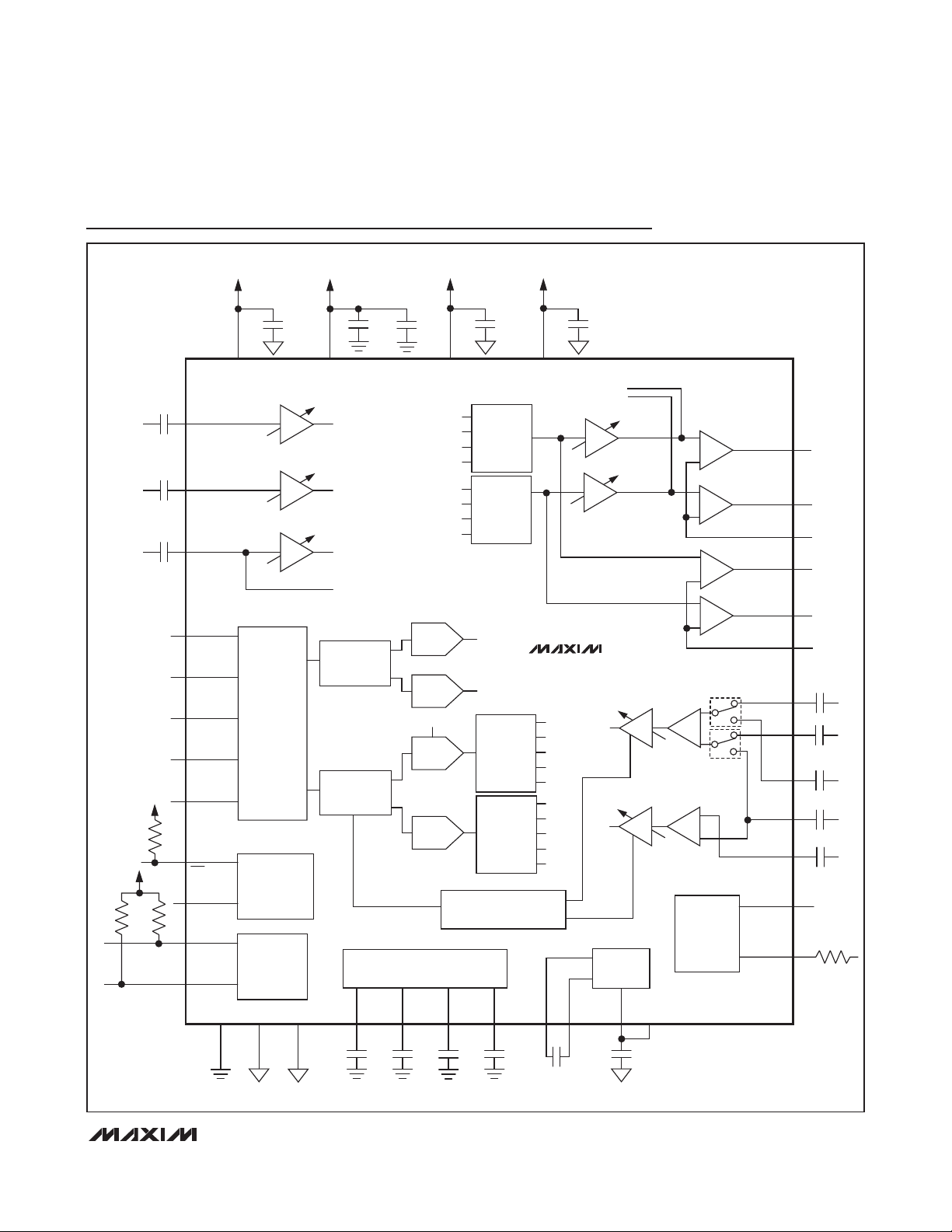
Functional Diagram
10kΩ
DVDD
10kΩ
10kΩ
DVDD
1μF
1μF
1μF
29
24
25
27
26
23
30
21
22
1
2
3
1.71V TO 3.6V
LINEIN1
LINEIN2
AUXIN
LRCLK_A
LRCLK_D
BCLK
SDIN
SDOUT
IRQ
MCLK
SCL
SDA
AGND
39
20
CPVDD
DIGITAL AUDIO
INTERFACE
TIMING AND
CONTROL LOGIC
2
I
DGND
32
4.7μF
-32dB TO +30dB
PGA
-32dB TO +30dB
PGA
-32dB TO +30dB
PGA
C SERIAL
PORT
CPGND
18
12
AVDD
LN1
LN2
AUXAC
AUXDC
DIGITAL
FILTERING AND
GAIN
DIGITAL
FILTERING AND
GAIN
1μF
1.71V TO 3.6V
0.1μF
PREG
4
10μF
LEFT
DAC
RIGHT
DAC
AUXDC
LEFT
ADC
RIGHT
ADC
INTERNAL REGULATORS
NREG
5
1μF
1μF
1μF
31
DVDD
MICL
LEFT AUDIO
LN1
OUTPUT
LN2
DACL
MICR
DACR
MIXER
RIGHT AUDIO
LN1
OUTPUT
LN2
MIXER
DACL
DACR
LEFT ADC
INPUT MIXER
RIGHT ADC
INPUT MIXER
AUTOMATIC GAIN CONTROL
MBIAS
REF
7
6
1μF
28
DVDDS2
MAX9856
AUXAC
LN1
LN2
MICL
MICR
AUXAC
LN1
LN2
MICL
MICR
C1N
C1
4.7μF
1μF
AUXAC
-73dB
TO +6dB
PGA
-73dB
TO +6dB
PGA
0 TO 20dB
MICL
PGA
PREAMPLIFIER
0 TO 20dB
MICR
PGA
PREAMPLIFIER
CHARGE
PUMP
C1P SVSS
PVSS
1917
16
C2
4.7μF
15
0
20dB
30dB
0
20dB
30dB
MICROPHONE
BIAS AND
JACK
DETECTION
HPL
HPR
HGNDSNS
LOUTL
LOUTR
LGNDSNS
INLP
INLN
MICL
MICGND
MICR
JACKSNS
MICBIAS
13
14
11
9
10
8
1μF
34
1μF
33
1μF
35
36
1μF
37
1μF
40
2.2kΩ
38
Page 18

MAX9856
Low-Power Audio CODEC with
DirectDrive Headphone Amplifiers
18 ______________________________________________________________________________________
Detailed Description
The MAX9856 is a high-performance, low-power stereo
audio CODEC designed to provide a complete audio
solution. Operating from a 1.8V supply, the MAX9856
achieves high performance and reasonable output power
while consuming only 9mW in DAC playback mode.
The internal 18-bit sigma-delta DAC accepts stereo digital audio signals, and converts them to stereo audio
outputs that can be mixed with line inputs and/or microphone inputs. The DAC is capable of operating at sample rates ranging from 8kHz to 96kHz with any master
clock frequency between 10MHz and 60MHz. The DAC
is capable of operating at a different sample rate than
the ADC. Both master and slave modes are available
when operating the interface in left-justified, I2S or PCM
data format. The incoming data can be level shifted and
highpass filtered in the digital domain. The highpass filtering allows only reproducible frequencies to be converted, saving power and improving sound quality.
The MAX9856 features stereo DirectDrive headphone
amplifiers and line outputs, which eliminate the need for
large output-coupling capacitors. The audio output path
includes high-quality mixing amplifiers to allow flexibility
in choosing from the DAC output and the stereo analog
line inputs. Volume control amplifiers provide adjustable
gains between +5.5dB and -74dB for the headphones.
The line outputs are capable of generating a 1V
RMS
out-
put signal from a full-scale digital input.
The digital audio signals of the internal 18-bit sigmadelta ADC outputs are converted from the analog microphone and line input paths. The ADC is capable of
operating at a sample rate ranging from 8kHz to 48kHz
with any master clock frequency between 10MHz and
60MHz. The ADC is capable of operating at a different
sample rate than the DAC. Both master and slave
modes are available when operating the interface in leftjustified, I2S, or PCM data formats. The outgoing data
can be level shifted and highpass filtered in the digital
domain. The highpass filtering allows reduction of wind
noise from microphone inputs.
Three microphone inputs are available. One fully differential input can be used with internal microphones
while a pair of single-ended inputs can be used with an
external mono or stereo headset microphone.
Selectable gain of 0dB, 20dB, and 30dB can be
applied to the input signals in addition to a 0 to 20dB
input PGA. The MAX9856 features AGC on the microphone input path to automatically compensate for varying input signal levels and the limited dynamic range of
most microphones. The integrated noise gate provides
low-level audio noise quieting to lower the audible
noise floor.
An auxiliary input is available for sending externally
generated beeps and sound effects directly to the
headphones. The auxiliary input can also be used to
make DC measurements with the ADC by providing a
direct path to the ADC.
HPL, HPR, and JACKSNS provide a headset detection
feature which can both detect the insertion of a jack
and measure the load impedance. Jack detection can
be done in both shutdown and powered-on mode. The
headphone and line outputs feature ground sensing to
reduce ground noise. Reduced output offset voltage
and extensive click-and-pop suppression circuitry on
headphone amplifiers eliminate audible clicks and
pops at startup and shutdown
I2C Register Address Map
and Definitions
The MAX9856 has 28 internal registers used for configuration and status reporting. Table 1 lists all the registers, their addresses, and power-on-reset (POR) states.
Registers 0x00 and 0x01 are read only, while all the
other registers are read/write. Write zeros to all unused
bits in the register table when updating the register,
unless otherwise noted.
Page 19

MAX9856
Low-Power Audio CODEC with
DirectDrive Headphone Amplifiers
______________________________________________________________________________________ 19
Table 1. Register Map
REGISTER B7 B6 B5 B4 B3 B2 B1 B0
Status CLD SLD ULK JKMIC HPOCL HPOCR JDET GPI 0x00 —
Status LSNS JKSNS HSDETL HSDETR JSDET 0x01 —
Interrupt Enable ICLD ISLD IULK 0 IHPOCL IHPOCR IJDET IGPI 0x02 0x00
CLOCK CONTROL
Clock Rates 0 PSCLK MAS BSEL 0x03 0x00
DAC INTERFACE
System DWCI DBCI DRATE DDLY PCM DHF WS 0x04
Interface DPLLEN DACNI[14:8] 0x05 0x00
Interface DACNI[7:0] 0x06 0x00
ADC INTERFACE
System AWCI ABCI APIN ADLY 0 0 0 0x07 0x00
Interface APLLEN ADCNI[14:8] 0x08 0x00
Interface ADCNI[7:0] 0x09 0x00
Level AGAIN ANTH 0x0A 0x00
DIGITAL FILTERS
Highpass Filters 0 ADCHP 0 DACHP 0x0B 0x00
AUTOMATIC GAIN CONTROL
AGC Control 0 AGCRLS AGCATK AGCHLD 0x0C 0x00
AGC Threshold 0 0 0 AGCSRC AGCSTH 0x0D 0x00
ANALOG MIXERS
ADC Mixer 0 0 0 MXINL 0x0E 0x00
ADC Mixer 0 0 0 MXINR 0x0F 0x00
Output Mixer MXOUTL MXOUTR 0x10 0x00
AUDIO INPUTS
Digital Input
Gain
AUXIN Gain 0 0 0 PGAAUX 0x12 0x00
LINEIN1 Gain 0 0 0 PGAL1 0x13 0x00
LINEIN2 Gain 0 0 0 PGAL2 0x14 0x00
MICL Gain 0 PAENL PGAML 0x15 0x00
MICR Gain 0 PAENR PGAMR 0x16 0x00
MIC Mode 0 0 0 0 MMIC MBSEL 0 LMICDIF 0x17 0x00
AUDIO OUTPUTS
HPL Volume 0 HPMUTE HPVOLL 0x18 0x00
HPR Volume 0 0 HPVOLR 0x19 0x00
Output Mode 0 VSEN AUXDC AUXMIX 0 0 HPMODE 0x1A 0x00
HEADSET DETECT
System 0 0 0 0 JDETEN EN 0x1B 0x00
POWER MANAGEMENT
System SHDN 0 DIGEN LOUTEN DALEN DAREN ADLEN ADREN 0x1C 0x00
PGADS 0x11 0x00
REGISTER
ADDRESS
POWER-ON
RESET
STATE
Page 20

MAX9856
Low-Power Audio CODEC with
DirectDrive Headphone Amplifiers
20 ______________________________________________________________________________________
Status Registers
Status registers 0x00 and 0x01 are read-only registers
that report the status of various device functions. The
status register bits are cleared upon a read operation of
the status register and are set the next time the event
occurs. Table 2 lists the status registers bit location and
description.
Table 2. Status Registers Bit Location
Status Register Bit Description
REG B7 B6 B5 B4 B3 B2 B1 B0
0x00 CLD SLD ULK JKMIC HPOCL HPOCR JDET GPI
0x01 LSNS JKSNS HSDETL HSDETR JSDET
BIT FUNCTION
CLD Clip Detect Flag. Indicates that a signal has become clipped in the ADC.
SLD
ULK
JKMIC
HPOCL/
HPOCR
JDET Headset Configuration Change Flag. Indicates a change in JKMIC, LSNS, or JKSNS.
GPI GPI State. Indicates the state of LRCLK_A when configured as a general-purpose input.
LSNS
Slew-Level Detect Flag. When volume or gain changes are made, the slewing circuitry smoothly steps through all
intermediate settings. When SLD is set high, all slewing has completed and the volume or gain is at its final value.
Digital PLL Unlock Flag. Indicates that the digital audio PLL for the DAC or ADC has become unlocked and digital
signal data is not reliable.
Jack Microphone Flag. Indicates JACKSNS has been pulled up to the MICBIAS voltage. The microphone bias
must be enabled for this bit to function properly.
Headphone Output Left/Right Current Overload Flags. Indicate that the headphone output amplifiers have
exceeded the rated current.
Headphone Sense. LSNS is set when the internal pullup current forces the voltage at HPL to exceed AVDD - 0.4V.
This indicates headphone jack insertion or removal has occurred. HPMODE must be set to 00 and JDETEN set to
1 for this bit to function.
JKSNS
HSDETL,
HSDETR,
JSDET
Jack S ense. JKS N S i s set w hen the i nter nal p ul l up cur r ent for ces the vol tag e on JAC KS N S to exceed AVDD - 0.4V .
Thi s i nd i cates j ack i nser ti on or r em oval has occur r ed . JD E TE N m ust b e set for thi s b i t to functi on.
Load Impedance Sense. Indicates the approximate load connected to HPR, HPL, or JACKSNS. These bits are
updated once each time the appropriate EN bits are set high and cause an undefeatable hardware interrupt.
BITS HEADPHONE OR JACKSNS LOAD
00 200Ω < load < open
01 50Ω < load < 200Ω
10 0 < load < 50Ω
11 Idle state
Page 21

MAX9856
Low-Power Audio CODEC with
DirectDrive Headphone Amplifiers
______________________________________________________________________________________ 21
Interrupt Enables
Hardware interrupts are reported on the open-drain IRQ
pin. When an interrupt occurs, IRQ remains low until the
interrupt is serviced by reading status register 0x00. If a
flag is set, it is reported as a hardware interrupt only if
the corresponding interrupt enable is set. Each bit
enables interrupts for the status flag in the respective bit
location in register 0x00. Table 3 lists the interrupt enable
bit locations and description.
Table 3. Interrupt Enable Bit Locations
Table 4. Clock Control Register
Clock Control Register Bit Description
Clock Control
The MAX9856 can work with a master clock supplied
from any system clock (MCLK) within the range of
10MHz to 60MHz range. A clock prescaler divides by
1, 2, or 4 to create an internal clock (PCLK) in the
10MHz to 20MHz range.
There are two clock-generation circuits that operate
independently for the ADC and DAC path, allowing the
ADC and DAC to be operated at different sample rates.
BCLK services the LRCLK signals for both the ADC and
DAC. When the ADC and DAC operate at different
LRCLK rates, BCLK should be set appropriately for the
higher sample rate. The number of clock cycles per
frame must be greater than or equal to the configured
bit depth.
The MAX9856 digital audio interface can operate in
either master or slave mode. In master mode, the
MAX9856 generates the BCLK and LRCLK signals,
which control the data flow on the digital audio interface. In slave mode, the external master device generates the BCLK and LRCLK signals. See Table 4.
REG B7 B6 B5 B4 B3 B2 B1 B0
0x02 ICLD ISLD IULK 0 IHPOCL IHPOCR IJDET IGPI
REG B7 B6 B5 B4 B3 B2 B1 B0
0x03 0 PSCLK MAS BSEL
BITS FUNCTION
MCLK Prescaler. Set PSCLK to appropriately divide down MCLK to a usable frequency:
000—Disable clock input
001—10MHz ≤ MCLK ≤ 16MHz (PCLK = MCLK/1)
PSCLK
MAS
BSEL
010—16MHz ≤ MCLK ≤ 20MHz (PCLK = MCLK/1)
011—20MHz ≤ MCLK ≤ 32MHz (PCLK = MCLK/2)
100—32MHz ≤ MCLK ≤ 40MHz (PCLK = MCLK/2)
101—40MHz ≤ MCLK ≤ 60MHz (PCLK = MCLK/4)
110—Reserved
111—Reserved
Master Mode. Selects between master and slave operation:
0 = Slave mode (BCLK, LRCLK_D, and LRCLK_A are inputs)
1 = Master mode (BCLK, LRCLK_D, and LRCLK_A are outputs)
BCLK Select. Configures BCLK when operating in master mode. Set BSEL to be a sufficiently high frequency to
fully clock in all data bits for both the DAC and ADC, if operating at different sample rates:
000—Off
001—Off
010—BCLK = 48 x LRCLK_D (recommended if the DAC and ADC operate at the same rate)
011—BCLK = 48 x LRCLK_A
100—BCLK = PCLK/2 (recommended if the DAC and ADC are not operating at the same rate)
101—BCLK = PCLK/4
110—BCLK = PCLK/8
111—BCLK = PCLK/16
Page 22

MAX9856
DAC Interface
The MAX9856 DAC is capable of supporting any sample rate from 8kHz to 96kHz in either master or slave
mode, including all common sample rates (8kHz,
11.025kHz, 12kHz, 16kHz, 22.05kHz, 24kHz, 32kHz,
44.1kHz, 48kHz, 88.2kHz and 96kHz).
A 15-bit clock divider coefficient must be programmed
into the device to set the DAC sample rate relative to
the prescaled MCLK input (PCLK). This allows high
flexibility in both the MCLK and LRCLK_D frequencies.
In slave mode, the interface accepts any LRCLK_D signal between 7.8kHz to 100kHz.
There are two speed settings for the DAC set by the
DRATE control bits. The highest rate runs the modulator
at an internal clock rate between 5MHz and 10MHz,
and provides the highest audio performance. The low
rate runs the modulator between 2.5MHz and 5MHz for
reduced power consumption.
The digital audio interface offers full functionality for
several digital audio formats including left-justified, I
2
S,
and PCM modes (Figure 1). Figure 2 shows the digital
timing for various modes. Table 5 shows the DAC interface registers and descriptions. Table 6 lists the common
DACNI and ADCNI values.
Low-Power Audio CODEC with
DirectDrive Headphone Amplifiers
22 ______________________________________________________________________________________
Table 5. DAC Interface Registers
DAC Interface Register Bit Descriptions
REG B7 B6 B5 B4 B3 B2 B1 B0
0x04 DWCI DBCI DRATE DDLY PCM DHF WS
0x05 DPLLEN DACNI[14:8]
0x06 DACNI[7:0]
REGISTER FUNCTION
DAC Word Clock (LRCLK_D) Invert
When PCM = 0:
0—Left-channel data is transmitted while LRCLK_D is low.
DWCI
1—Right-channel data is transmitted while LRCLK_D is low.
When PCM = 1:
0—Start of a new frame is signified by the falling edge of the LRCLK_D pulse.
1—Start of a new frame is signified by the rising edge of the LRCLK_D pulse.
DAC BCLK Invert:
0—SDIN is accepted on the rising edge of BCLK.
DBCI
DRATE
DDLY
1—SDIN is accepted on the falling edge of BCLK.
In master mode:
0—LRCLK_D transitions occur on the falling edge of BCLK.
1—LRCLK_D transitions occur on the rising edge of BCLK.
DAC Modulator Rate:
00—Low-power mode
01—Reserved
10—High-performance mode
11—DAC clock disabled
DAC Data Delay:
0—The most significant bit of an audio word is latched at the first BCLK edge after the
LRCLK_D transition.
1—The most significant bit of an audio word is latched at the second BCLK edge after the
LRCLK_D transition.
2
(DDLY = 1 for I
S-compatible mode)
Page 23

MAX9856
Low-Power Audio CODEC with
DirectDrive Headphone Amplifiers
______________________________________________________________________________________ 23
DAC Interface Register Bit Descriptions (continued)
Table 6. Common DACNI and ADCNI Values
Note: Values in bold are exact integers that provide maximum full-scale performance.
REGISTER FUNCTION
PCM Mode Select. PCM determines the format of the LRCLK_D and LRCLK_A signal:
0—The LRCLK_D and LRCLK_A signals have a 50% duty cycle. Left-channel audio is
transmitted during one state of and right-channel audio during the other state.
PCM
DHF
WS
DPLLEN
DACNI
1—LRCLK_D and LRCLK_A are pulses that indicate the start of a frame of audio data
consisting of two channels. Following the frame sync pulse, 16 bits of left-channel data is
immediately followed by 16 bits of right-channel data. The DDLY and WS bits are ignored when
PCM = 1.
DAC High-Sample Rate Mode:
0—LRCLK_D is less than 50kHz. 8x FIR interpolation filter used.
1—LRCLK_D is greater than 50kHz. 4x FIR interpolation filter used.
Word Size. This bit controls both the DAC and ADC:
0—16 bits.
1—18 bits.
The DAC interface can accept higher than 18-bit words but the additional least significant bits
are ignored.
DAC PLL Enable:
0 (valid for slave and master mode)—The frequency of LRCLK_D is set by the DACNI divider
bits. In master mode, the MAX9856 generates LRCLK_D using the specified divide ratio. In
slave mode, the MAX9856 expects an LRCLK_D as specified by the divide ratio.
1 (valid for slave mode only)—A digital PLL locks on to any externally supplied LRCLK_D signal
regardless of the MCLK frequency. DHF must set high for sample rates above 50kHz.
DAC LRCLK Divider. When DPLLEN is set low, the frequency of LRCLK_D is determined by
DACNI. See Table 6 for common DACNI values:
DACNI = (65536 x 96 x f
DACNI = (65536 x 48 x f
f
LRCLK_D
f
PCLK
= LRCLK_D frequency.
= Prescaled MCLK internal clock frequency (PCLK).
LRCLK_D
LRCLK_D
)/f
)/f
PCLK
PCLK
for (DHF = 0).
for (DHF = 1).
LRCLK
MCLK (MHz) PSCLK 8kHz 16kHz 32kHz 44.1kHz 48kHz 88.2kHz (DAC ONLY) 96kHz (DAC ONLY)
11.2896 001 116A 22D4 45A9 6000 687D 6000 687D
12 001 1062 20C5 4189 5A51 624E 5A51 624E
12.288 001 1000 2000 4000 5833 6000 5833 6000
13 001 F20 1E3F 3C7F 535F 5ABE 535F 5ABE
16.9344 010 B9C 1738 2E71 4000 45A9 4000 45A9
18.432 010 AAB 1555 2AAB 3ACD 4000 3ACD 4000
19.2 010 960 4B0 258 1B3 190 1B3 190
24 011 1062 20C5 4189 5A51 624E 5A51 624E
26 011 F20 1E3F 3C7F 535F 5ABE 535F 5ABE
27 011 E90 1D21 3A41 5048 5762 5048 5762
Page 24

MAX9856
Low-Power Audio CODEC with
DirectDrive Headphone Amplifiers
24 ______________________________________________________________________________________
Figure 1. Digital Audio Interface Data Format Examples
DIGITAL AUDIO INTERFACE SLAVE MODES: (LRCLK SHOULD TRANSITION ON THE UNUSED BCLK EDGE)
DWCI/AWCI = 0, DBCI/ABCI = 0, DDLY/ADLY = 0, WS = 0, PCM = 0
LEFT RIGHT
D15 D14 D13 D12 D11 D10 D9 D8 D7 D6 D5 D4 D3 D2 D1 D0
DWCI/AWCI = 1, DBCI/ABCI = 1, DDLY/ADLY = 0, WS = 0, PCM = 0
D15 D14 D13 D12 D11 D10 D9 D8 D7 D6 D5 D4 D3 D2 D1 D0
DWCI/AWCI = 0, DBCI/ABCI = 0, DDLY/ADLY = 1, WS = 1, PCM = 0
D17
D16 D15 D14 D13 D12 D11 D10 D9 D 8 D7 D6 D5 D 4 D 3 D 2 D 1 D 0 D17 D16 D15 D14 D13 D12 D11 D10 D 9 D 8 D7 D6 D 5 D 4 D3 D2 D1 D 0
DWCI/AWCI = 0, DBCI/ABCI = 0, DDLY/ADLY = 0, WS = 0, PCM = 1
LEFT RIGHT
D15 D14 D13 D12 D11 D10 D9 D 8 D 7 D 6 D 5 D 4 D3 D 2 D1 D0 D15 D14 D13 D12 D11 D10 D9 D 8 D 7 D 6 D5 D4D3D2 D1 D0
DIGITAL AUDIO INTERFACE MASTER MODE:
DWCI/AWCI = 0, DBCI/ABCI = 0, DDLY/ADLY = 0, WS = 0, PCM = 0
LEFT RIGHT
D15 D14 D13 D12 D11 D10 D9 D8 D7 D6 D5 D4 D3 D2 D1 D0
LEFT RIGHT
D15 D14 D13 D12 D11 D10 D9 D8 D7 D6 D5 D4 D3 D2 D1 D0
LEFT
RIGHT
D15 D14 D13 D12 D11 D10 D9 D8 D7 D6 D5 D4 D3 D2 D1 D0
DWCI/AWCI = 0, DBCI/ABCI = 0, DDLY/ADLY = 1, WS = 0, PCM = 0
LEFT RIGHT
D15 D14 D13 D12 D11 D10 D9 D8 D7 D6 D5 D4 D3 D2 D1 D0
D15 D14 D13 D12 D11 D10 D9 D8 D 7 D6 D5 D 4 D 3 D 2 D 1 D 0
D13 D12 D11 D10 D9 D8 D7 D6 D5 D4 D3 D2 D1 D0
D14
D15
Page 25

MAX9856
Low-Power Audio CODEC with
DirectDrive Headphone Amplifiers
______________________________________________________________________________________ 25
ADC Interface
The stereo ADC is capable of outputting data at any
sample rate from 8kHz to 48kHz. Data can be output in
common formats including left justified, I2S, and PCM
(Figure 1). Figure 2 shows the digital timing in both
slave and master modes.
If the DAC and ADC operate at the same sample rate
only the LRCLK_D is needed, allowing the LRCLK_A
pin to be reassigned as a GPIO. When configured as a
general-purpose output, LRCLK_A can be set high or
low by the APIN bits. When configured as a generalpurpose input, the status is reported in register 0x00.
Table 7 lists and describes the ADC interface registers.
Figure 2. Digital Audio Interface Timing Diagrams
Table 7. ADC Interface Registers
ADC Interface Register Bit Description
DAI STEREO SERIAL INTERFACE TIMING DIAGRAM (SLAVE MODE)
DAI STEREO SERIAL INTERFACE TIMING DIAGRAM (MASTER MODE)
SDIN/LRCLK (INPUTS)
t
t
SU
BCLK (BCI = 0, INPUT)
BCLK (BCI = 1, INPUT)
SDOUT (OUTPUT)
t
r, tf
t
DLY
t
HD
BCLKH, tBCLKL
t
BCLKS
SDIN (INPUT)
t
BCLKH, tBCLKL
t
BCLKM
BCLK (OUTPUT)
SDOUT/LRCLK (OUTPUTS)
t
SU
t
r, tf
t
DLY
t
HD
REG B7 B6 B5 B4 B3 B2 B1 B0
0x07 AWCI ABCI APIN ADLY 0 0 0
0x08 APLLEN ADCNI[14:8]
0x09 ADCNI[7:0]
0x0A AGAIN ANTH
REGISTER FUNCTION
ADC Word Clock (LRCLK_A) Invert
When PCM = 0:
0—Left-channel data is transmitted while LRCLK_A is low.
AWCI
ABCI
1—Right-channel data is transmitted while LRCLK_A is low.
When PCM = 1:
0—Start of a new frame is signified by the falling edge of the LRCLK_A pulse.
1—Start of a new frame is signified by the rising edge of the LRCLK_A pulse.
ADC BCLK Invert:
0—SDOUT is valid on the rising edge of BCLK.
1—SDOUT is valid on the falling edge of BCLK.
If operating in master mode, the ABCI bit has no effect. The DBCI bit controls BCLK to LRCLK_A
timing.
Page 26

MAX9856
Low-Power Audio CODEC with
DirectDrive Headphone Amplifiers
26 ______________________________________________________________________________________
ADC Interface Register Bit Description (continued)
REGISTER FUNCTION
LRCLK_A/GPIO Configuration:
00 = General-purpose input
01 = Word clock for the ADC
APIN
ADLY
APLLEN
ADCNI
AGAIN
10 = General-purpose output—low
11 = General-purpose output—high
When APIN ≠ 01, LRCLK_D is used as the word clock for both the DAC and ADC. AWCI, ABCI, and
ADLY are still active and independent from the DAC mode bit settings when operating with a shared
LRCLK_D.
ADC Data Delay
0—The most significant bit of an audio word is valid at the first BCLK edge after the LRCLK_A
transition.
1—The most significant bit of an audio word is valid at the second BCLK edge after the LRCLK_A
transition.
(ADLY = 1 for I
ADC PLL Enable. This bit only applies when APIN = 01. When APIN ≠ 01 use DPLLEN for both the
DAC and ADC:
0 (Valid for slave and master mode)—The frequency of LRCLK_A is set by the ADCNI divider bits. In
master mode, the MAX9856 generates LRCLK_A using the specified divide ratio. In slave mode, the
MAX9856 expects an LRCLK_A using specified divide ratio.
1 (Valid for slave mode only)—A digital PLL locks on to any externally supplied LRCLK_A signal
regardless of the MCLK frequency.
ADC LRCLK Divider. If APIN ≠ 01, use DACNI for both the DAC and ADC. When APLLEN is set low,
the frequency of LRCLK_A is determined by ADCNI. See Table 6 for common ADCNI values:
ADCNI = (65536 x 96 x f
f
LRCLK_A
f
= Prescaled MCLK internal clock frequency (PCLK).
PCLK
ADC Output Gain. Specifies the gain applied to the digital output of the ADC prior to being output
from the device.
2
S-compatible mode)
LRCLK_A
= LRCLK_A frequency.
VALUE GAIN (dB)
0x0 +3
0x1 +2
0x2 +1
0x3 0
0x4 -1
0x5 -2
0x6 -3
0x7 -4
0x8 -5
0x9 -6
0xA -7
0xB -8
0xC -9
0xD -10
0xE -11
0xF -12
)/f
PCLK
.
Page 27

MAX9856
Low-Power Audio CODEC with
DirectDrive Headphone Amplifiers
______________________________________________________________________________________ 27
ADC Interface Register Bit Description (continued)
Digital Filters
The MAX9856 digital audio interface includes digital
first-order highpass filters (Table 8) for both the DAC
input and the ADC output. The corner frequency for
each filter is selectable from 5Hz to 4kHz. The DAC filter (DACHP) can be used to reduce the low-frequency
energy sent to speakers incapable of reproducing low
frequencies. The ADC filter (ADCHP) can reduce lowfrequency noise such as wind noise from being converted. The cutoff frequency depends on sample rate
and is shown in Table 9.
Table 8. Digital Highpass Filters
REGISTER FUNCTION
ADC Noise Gate Threshold. The MAX9856 features a noise gate that reduces the audible noise at
low signal levels. The noise gate attenuates the output at a rate of 1dB for each 2dB the signal is
below the threshold. ANTH specifies the noise gate threshold level relative to the final ADC output
signal level.
The noise gate can be used in conjunction with AGC or on its own. When AGC is enabled, the noise
gate reduces the output level only when the AGC has set the gain to the maximum setting. Choose a
threshold between -28dB and -48dB when used in conjunction with the AGC. When the AGC is
enabled, the effective noise gate thresholds are increased by 20dB due to the microphone PGA
being set to maximum gain by the AGC.
ADC NOISE GATE THRESHOLD LEVELS
ANTH
VALUE THRESHOLD (dB)
0x0 to 0x5 Disabled
0x6 -64
0x7 -60
0x8 -56
0x9 -52
0xA -48
0xB -44
0xC -40
0xD -36
0xE -32
0xF -28
REG B7 B6 B5 B4 B3 B2 B1 B0
0x0B 0 ADCHP 0 DACHP
Page 28
MAX9856
Automatic Gain Control
The MAX9856 AGC continuously adjusts the analog
microphone PGAs to maintain constant signal level. When
the AGC is enabled, manual control of the input PGA is
not possible. The PGA includes zero-cross detection,
which prevents gain changes, from being audible.
The AGC process consists of three main sections.
When the AGC threshold is exceeded, the gain is
reduced exponentially with a time constant referred to
as the attack time. Once the large signal has passed,
the AGC waits the specified hold time before reducing
the gain. The time required to reduce the gain from
maximum attenuation to minimum attenuation is known
as the release time.
The AGC circuitry only operates on the PGA in the microphone path, but the digital level detector is based on the
mixed signal. Only use the AGC when input signals from
the LINEIN and AUXIN are excluded or attenuated.
Table 10 lists the AGC registers and shows the AGC
register bit description.
Low-Power Audio CODEC with
DirectDrive Headphone Amplifiers
28 ______________________________________________________________________________________
Table 9. Digital Highpass Filter Cutoff Frequencies
Table 10. Automatic Gain Control Registers
AGC Register Bit Description
LRCLK (kHz)
8 Off 5 10 20 41 82 170 364
11.025 Off 7 14 28 56 114 235 501
12 Off 8 15 30 61 124 255 545
16 Off 10 20 40 81 165 340 727
22.05 Off 14 28 55 112 227 469 1002
24 Off 15 30 60 122 247 511 1091
32 Off 20 40 80 162 330 681 1455
44.1 Off 28 55 111 224 455 938 2005
48 Off 30 60 121 244 495 1021 2182
64 Off 40 80 161 325 660 1362 2909
88 Off 55 111 222 448 909 1877 4009
96 Off 60 120 241 487 990 2043 4364
000 001 (Hz) 010 (Hz) 011 (Hz) 100 (Hz) 101 (Hz) 110 (Hz) 111 (Hz)
ADCHP/DACHP
REG B7 B6 B5 B4 B3 B2 B1 B0
0x0C 0 AGCRLS AGCATK AGCHLD
0x0D 0 0 0 AGCSRC AGCSTH
BITS FUNCTION
AGC Release Time. The release time is the time it takes for the gain to return to its normal level after the
input signal has fallen below the threshold and the hold time has passed:
000—78ms
001—156ms
AGCRLS
010—312ms (recommended)
011—625ms
100—1.25s
101—2.5s
110—5s
111—10s
Page 29

MAX9856
Low-Power Audio CODEC with
DirectDrive Headphone Amplifiers
______________________________________________________________________________________ 29
AGC Register Bit Description (continued)
BITS FUNCTION
AGC Attack Time. The attack time is the time it takes to reduce the gain after the input signal has
exceeded the threshold level. The gain attenuation during attack is exponential and the attack time is
defined as one-time constant rather than the time it takes to reach the final gain:
AGCATK
AGCHLD
AGCSRC
AGCSTH
00—3ms
01—12ms
10—50ms (recommended)
11—200ms
AGC Hold Time. Hold time is the delay before the AGC release begins. The hold time counter starts
whenever the signal drops below the AGC threshold and is reset by any signal that exceeds the
threshold:
00—AGC disabled
01—50ms
10—100ms (recommended)
11—400ms
AGC and Noise Gate Signal Source. Selects the audio signal that the AGC and noise gate circuitry
monitors:
0—Left-channel ADC output
1—Left-channel + right channel ADC output (results in 3dB lower threshold for coherent signals)
AGC Threshold. Sets the signal level at which the AGC begins gain reduction. The signal is monitored
after the ADC output gain has been applied.
AGCSTH LEVEL (dB)
0000 -3
0001 -4
0010 -5
0011 -6
0100 -7
0101 -8
0110 -9
0111 -10
1000 -11
1001 -12
1010 -13
1011 -14
1100 -15
1101 -16
1110 -17
1111 -18
AGC THRESHOLD LEVELS
Page 30

MAX9856
Analog Mixers
The MAX9856 has two main analog mixers. The first
feeds signals into the headphone and line output
amplifiers while the second supplies the ADC input.
Each mixer is configurable independently for left and
right channels. See Table 11 for audio mixer control
registers and register bit description.
Low-Power Audio CODEC with
DirectDrive Headphone Amplifiers
30 ______________________________________________________________________________________
Table 11. Audio Mixer Control Registers
Audio Mixer Register Bit Description
REG B7 B6 B5 B4 B3 B2 B1 B0
0x0E 0 0 0 MXINL
0x0F 0 0 0 MXINR
0x10 MXOUTL MXOUTR
BITS FUNCTION
MXINL OR MXINR SELECTED INPUT SOURCE
MXINL/MXINR
MXOUTL OR MXOUTR SELECTED INPUT SOURCE
MXOUTL/MXOUTR
ADC INPUT MIXER DESCRIPTION
00000 No input source selected
1XXXX AUXOUT selected
X1XXX LINEIN1 selected
XX1XX LINEIN2 selected
XXX1X MICL selected
XXXX1 MICR selected
AUDIO OUTPUT MIXER DESCRIPTION
0000 No input source selected
1XXX MIC L/R PGA output selected
X1XX LINEIN1 selected
XX1X LINEIN2 selected
XXX1 DAC output selected
Page 31

Analog Inputs
The MAX9856 features various analog inputs. All inputs
have independent gain control for maximum flexibility.
AUXIN is a mono auxiliary input that can be used for
mixing alarms, beeps, and sound effects into the headphone outputs or ADC input. The AUXIN signal has a
dedicated PGA for gain adjustment and can be mixed
into the headphone output signal directly, bypassing
the output mixer and volume control. AUXIN can also
serve as an input for making precise measurements in
the system. In this mode, the PGA is bypassed,
increasing the impedance of the input, and is directly
connected to the ADC.
Three microphone inputs are available. Two are pseudodifferential inputs with a shared ground connected to the
inverting input of the microphone preamplifier. The third
is a fully differential input. Stereo microphones that share
a common return path can take advantage of the
pseudo-differential configuration by connecting the common return to the MICGND, canceling common-mode
noise. Figure 3 shows the typical application circuit for
both single-ended and differential microphones. The
microphone preamplifier and PGA provide a wide range
of gain options. The microphone inputs can also be used
as additional line inputs when the gain is set to 0dB.
A single low-noise bias voltage output is available
(MICBIAS) to bias microphones from a clean supply
with an external bias resistor. There are two selectable
microphone bias voltages that can be selected
depending on the power-supply voltage. Table 12 lists
the audio input control registers and bit description.
MAX9856
Low-Power Audio CODEC with
DirectDrive Headphone Amplifiers
______________________________________________________________________________________ 31
Table 12. Audio Input Control Registers
Figure 3. Typical Microphone Connections: (a) Pseudo-Differential, (b) Differential
MICBIAS
2.2kΩ
JACKSNS
MICL/MICR
MICBIAS
2.2kΩ
JACKSNS
INLP
MICGND
2.2kΩ
(a)
(b)
REG B7 B6 B5 B4 B3 B2 B1 B0
0x11 PGADS
0x12 0 0 0 PGAAUX
0x13 0 0 0 PGAL1
0x14 0 0 0 PGAL2
0x15 0 PAENL PGAML
0x16 0 PAENR PGAMR
0x17 0 0 0 0 MMIC MBSEL 0 LMICDIF
INLN
Page 32

MAX9856
Low-Power Audio CODEC with
DirectDrive Headphone Amplifiers
32 ______________________________________________________________________________________
Audio Input Register Bit Description
BITS FUNCTION
Programmable Gain Adjust for Digital Audio Input
SETTING GAIN (dB) SETTING GAIN (dB)
0x00 0 0x93 -15
0x07 -0.5 0x96 -15.5
0x0E -1 0x99 -16
0x15 -1.5 0x9C -16.5
0x1C -2 0x9F -17
0x22 -2.5 0xA2 -17.5
0x29 -3 0xA5 -18
0x2F -3.5 0xA7 -18.5
0x35 -4 0xAA -19
0x3A -4.5 0xAC -19.5
0x40 -5 0xAE -20
0x45 -5.5 0xB3 -21
0x4A -6 0xB7 -22
PGADS
0x50 -6.5 0xBB -23
0x55 -7 0xBF -24
0x59 -7.5 0xC2 -25
0x5E -8 0xC6 -26
0x63 -8.5 0xC9 -27
0x67 -9 0xCC -28
0x6B -9.5 0xCF -29
0x70 -10 0xD2 -30
0x74 -10.5 0xD4 -31
0x78 -11 0xD6 -32
0x7C -11.5 0xD9 -33
0x7F -12 0xDB -34
0x83 -12.5 0xDD -35
0x86 -13 0xDF -36
0x8A -13.5 0xE1 -37
0x8D -14 0xE2 -38
0x90 -14.5 0xE4 -39
— — 0xE5 -40
DIGITAL AUDIO INPUT PGA SETTINGS
Page 33

MAX9856
Low-Power Audio CODEC with
DirectDrive Headphone Amplifiers
______________________________________________________________________________________ 33
Audio Input Register Bit Description (continued)
BITS FUNCTION
Programmable Gain Adjust for Line Inputs
LINE INPUT PGA SETTINGS
SETTING GAIN (dB) SETTING GAIN (dB)
0x00 +30 0x10 -2
0x01 +28 0x11 -4
0x02 +26 0x12 -6
0x03 +24 0x13 -8
0x04 +22 0x14 -10
PGAAUX/
PGAL1/
PGAL2
0x05 +20 0x15 -12
0x06 +18 0x16 -14
0x07 +16 0x17 -16
0x08 +14 0x18 -18
0x09 +12 0x19 -20
0x0A +10 0x1A -22
0x0B +8 0x1B -24
0x0C +6 0x1C -26
0x0D +4 0x1D -28
0x0E +2 0x1E -30
0x0F +0 0x1F -32
Page 34

MAX9856
Low-Power Audio CODEC with
DirectDrive Headphone Amplifiers
34 ______________________________________________________________________________________
Audio Input Register Bit Description (continued)
BITS FUNCTION
Left/Right Programmable Gain Adjustment for Microphone Inputs. When AGC is enabled, the PGAML and
PGAMR bits cannot be manually programmed. The PGAML register can be monitored to determine the gain
set by the AGC.
MICROPHONE PGA SETTINGS
PGAML/
PGAMR
PAENL/PAENR
MMIC Microphone Mute Enable
Left/Right Microphone Preamplifier Enable. Enables the microphone circuitry and sets the preamplifier gain:
00—Microphones disabled
01—0dB
10—20dB
11—30dB
SETTING GAIN (dB) SETTING GAIN (dB)
0x00 +20 0x0B +9
0x01 +19 0x0C +8
0x02 +18 0x0D +7
0x03 +17 0x0E +6
0x04 +16 0x0F +5
0x05 +15 0x10 +4
0x06 +14 0x11 +3
0x07 +13 0x12 +2
0x08 +12 0x13 +1
0x09 +11 0x14 to 0x1F 0
0x0A +10 — —
MICBIAS Voltage Select:
MBSEL
LMICDIF
0—MICBIAS = 1.5V
1—MICBIAS = 2.4V (use only when AVDD ≥ 2.7V)
Left Microphone Input Select:
0—MICL/MICGND (pseudo-differential input)
1—INLP/INLN (differential input)
Page 35

MAX9856
Low-Power Audio CODEC with
DirectDrive Headphone Amplifiers
______________________________________________________________________________________ 35
Audio Outputs
The MAX9856 features stereo headphone amplifiers and
line output amplifiers with DirectDrive technology.
DirectDrive eliminates the need for bulky and expensive
DC-blocking capacitors on the outputs. The DirectDrive
biasing scheme is illustrated in Figure 4. The headphone outputs have separate left/right volume controls
while the line outputs produce a fixed level signal.
The audio outputs feature ground sensing, which is
intended to reduce the effect of ground noise. In many
systems, the ground return for line outputs and headphone jacks is used by other functions such as video
signals and microphone signals. The sharing of ground
can result in interference that is audible. The MAX9856’s
ground sense provides a path for the interfering signal to
be input and combined with the output audio signal to
reduce the audibility of the interference. Connect HGNDSNS directly to the ground terminal of the headphone jack
to enable ground sense on the headphones (Figure 5).
Similarly connect LGNDSNS directly to the ground terminal of a line output jack to enable ground sense on the
line outputs. If ground sense is not required, connect
HGNDSNS and LGNDSNS to AGND. Table 13 lists the
audio output control registers and bit description.
Figure 4. Traditional Amplifier Output vs. MAX9856 DirectDrive Output
Figure 5. Ground Sense Connection
AVDD
AVDD/2
AVDD
AGND
GND
CONVENTIONAL AMPLIFIER BIASING SCHEME
GND HPR HPL
SVSS
DirectDrive AMPLIFIER BIASING SCHEME
HPL
HPR
HGNDSNS
Page 36

MAX9856
Low-Power Audio CODEC with
DirectDrive Headphone Amplifiers
36 ______________________________________________________________________________________
Table 13. Audio Output Control Registers
Audio Output Register Bit Description
REGISTER B7 B6 B5 B4 B3 B2 B1 B0
0x18 0 HPMUTE HPVOLL
0x19 0 0 HPVOLR
0x1A 0 VSEN AUXDC AUXMIX 0 0 HPMODE
BITS FUNCTION
HPMUTE Headphone Mute Enable
Headphone Volume Control
HEADPHONE VOLUME-CONTROL SETTINGS
SETTING GAIN (dB) SETTING GAIN (dB) SETTING GAIN (dB)
0x00 +5.5 0x0E -8 0x1C -36
0x01 +5 0x0F -10 0x1D -38
0x02 +4.5 0x10 -12 0x1E -40
0x03 +4 0x11 -14 0x1F -42
0x04 +3.5 0x12 -16 0x20 -46
HPVOLL/HPVOLR
VSEN
0x05 +3 0x13 -18 0x21 -50
0x06 +2.5 0x14 -20 0x22 -54
0x07 +2 0x15 -22 0x23 -58
0x08 +1 0x16 -24 0x24 -62
0x09 0 0x17 -26 0x25 -66
0x0A -1 0x18 -28 0x26 -70
0x0B -2 0x19 -30 0x27 -74
0x0C -4 0x1A -32 0x28 to 0x3F Mute
0x0D -6 0x1B -34 — —
Volume Slewing Enable. Enables volume slewing so that when a volume change is made, the actual
volume control steps though all intermediate settings to give a smooth sounding change.
Auxiliary Input DC Measurement Mode:
AUXDC
AUXMIX
HPMODE
0—AUXIN connected to the input PGA for audio signals.
1—AUXIN directly connected to the ADC input for DC measurements.
Set MXINL to 10000 for proper operation.
Auxiliary Input Connected to Headphone Amplifiers:
0—AUXIN not connected to the headphone amplifiers.
1—AUXIN mixed directly into the headphone amplifiers bypassing the output mixer.
Headphone Output Mode:
00—Shutdown
01—Standard mono mode (HPL = mono, HPR = shutdown)
10—Dual mono mode (HPL = HPR = mono)
11—Stereo mode
Page 37

MAX9856
Low-Power Audio CODEC with
DirectDrive Headphone Amplifiers
______________________________________________________________________________________ 37
Headset Detection
The MAX9856 features headset detection that can detect
the insertion and removal of a jack as well as the load
type. When a jack is detected, an interrupt on IRQ can be
triggered to alert the microcontroller of the event. Figure 6
shows the typical configuration for jack detection and
Table 14 shows the headset detect control register and
bit description.
Sleep-Mode Jack Detection
When the MAX9856 is in shutdown and the power supply is available, sleep mode jack detection can be
enabled to detect jack insertion. Sleep mode applies a
2µA pullup current to JACKSNS and HPL, which forces
the voltage on JACKSNS and HPL to AVDD when no
load is applied. When a jack is inserted, either JACKSNS, HPL, or both are loaded sufficiently to reduce the
output voltage to nearly 0V and clear the JKSNS or
LSNS bits, respectively. The change in the LSNS and
JKSNS bits sets JDET and triggers an interrupt on IRQ
if IJDET is set. The interrupt signals the microcontroller
that a jack has been inserted, allowing the microcontroller to respond as desired.
Powered-On Jack Detection
When the MAX9856 is in normal operation and the
microphone interface is enabled, jack insertion and
removal can be detected through the JACKSNS pin. As
shown in Figure 6, V
MIC
is pulled up by MICBIAS.
When a microphone is connected, V
MIC
is assumed to
be between 0V and 95% of V
MICBIAS
. If the jack is
removed, V
MIC
increases to V
MICBIAS
. This event causes JKMIC to be set, alerting the system that the headset has been removed. Alternatively, if the jack is
inserted, V
MIC
decreases to below 95% of V
MICBIAS
and JKMIC is cleared, alerting that a jack has been
inserted. The JKMIC bit can be configured to create a
hardware interrupt that alerts the microcontroller of jack
removal and insertion events.
Impedance Detection
The MAX9856 is able to detect the type of load connected by applying a 2mA pullup current to HPL, HPR,
and JACKSNS. To minimize click-and-pop the current
is ramped up and down over a 24ms period. The 2mA
current can be individually applied to HPL, HPR, and
JACKSNS by appropriately configuring the EN bits.
When the 2mA current has finished ramping, HSDETL,
HSDETR, and JSDET are updated to reflect the measured impedance. EN must be cleared and reset to remeasure the impedance. Figure 7 and Table 15
illustrate the impedance detection process.
Figure 6. Example Jack Configuration for Jack Detection
Figure 7. Current on HPL, HPR, or JACKSNS During Impedance Detection
HPL
GND MIC HPR HPL
HPR
I
SET EN BITS TO 1
2mA
t
O
READ HSDETL,
HSDETR,
JSDET
tO + 24ms
SET EN BITS TO 0
- 24ms
t
f
MICBIAS
JACKSNS
MICL
IMPEDANCE
DETECTION
COMPLETE
t
f
Page 38

MAX9856
Low-Power Audio CODEC with
DirectDrive Headphone Amplifiers
38 ______________________________________________________________________________________
Table 15. Impedance Detection Routine
Table 14. Headset Detect Control Register
Headset Detection Register Bit Description
REG B7 B6 B5 B4 B3 B2 B1 B0
0x1B 0 0 0 0 JDETEN EN
TIME EVENT
t
0
t0 + 24ms
tf -24ms
t
f
BIT FUNCTION
Disable the headphone amplifiers. Set EN = 111 to enable the detection circuitry.
IRQ set high. Indicates that the detection current has reached its final value and the impedance has been
stored in HSDETL, HSDETR, and JSDET.
Once the impedance of HPL, HPR, and JACKSNS has been read, set EN = 000 to shut down the detection
circuitry.
IRQ set high. Indicates that the detection circuitry is completely shut down and the headphone amplifiers can
be reenabled.
Jack Detection Enable
JDETEN
EN
Sleep Mode—Enables pullups on HPL and JACKSNS to detect jack insertion. LSNS and JKSNS are not
valid unless JDETEN = 1 and SHDN = 0.
Normal Mode—Enables the comparator circuitry on JACKSNS to detect voltage changes. JKMIC is not valid
unless JDETEN = 1 and the microphone circuitry is enabled.
Impedance Detection Enable. Enables the impedance detection circuitry for HPL, HPR, and JACKSNS.
When EN = 000 HSDETL, HSDETR, and JSDET are set to 11. See Table 2, Status Register Bit Description
for details on reading the load impedance.
IMPEDANCE DETECTION ENABLE DESCRIPTION
EN DESCRIPTION
000 Disabled
1xx JACKSNS pin impedance sense enabled
x1x HPR pin impedance sense enabled
xx1 HPL pin impedance sense enabled
Page 39
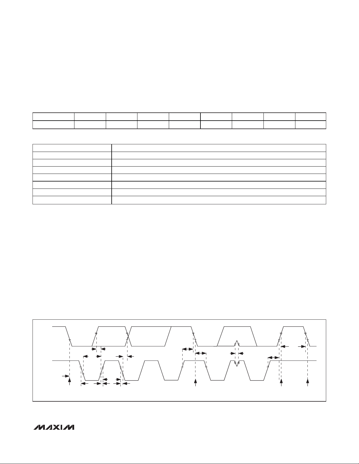
MAX9856
Low-Power Audio CODEC with
DirectDrive Headphone Amplifiers
______________________________________________________________________________________ 39
Power Management and Control
The MAX9856 has comprehensive power management
that allows unused features to be disabled, thereby
saving power. Table 16 shows the power/management
register and a register bit description.
Table 16. Power-Management Register
Power-Management Register Bit Description
SMBus is a trademark of Intel Corp.
Figure 8. 2-Wire Interface Timing Diagram
I2C Serial Interface
The MAX9856 features an I2C/SMBus™-compatible,
2-wire serial interface consisting of a serial-data line
(SDA) and a serial-clock line (SCL). SDA and SCL facilitate communication between the MAX9856 and the
master at clock rates up to 400kHz. Figure 8 shows the
2-wire interface timing diagram. The master generates
SCL and initiates data transfer on the bus. The master
device writes data to the MAX9856 by transmitting the
proper slave address followed by the register address
and then the data word. Each transmit sequence is
framed by a START (S) or REPEATED START (Sr) condition and a STOP (P) condition. Each word transmitted
to the MAX9856 is 8 bits long and is followed by an
acknowledge clock pulse. A master reading data from
the MAX9856 transmits the proper slave address
followed by a series of nine SCL pulses. The MAX9856
transmits data on SDA in sync with the master-generated
SCL pulses. The master acknowledges receipt of each
byte of data. Each read sequence is framed by a
START or REPEATED START condition, a not acknowledge, and a STOP condition. SDA operates as both an
input and an open-drain output. A pullup resistor, typically greater than 500Ω, is required on SDA. SCL operates only as an input. A pullup resistor, typically
greater than 500Ω, is required on SCL if there are multiple masters on the bus, or if the single master has an
open-drain SCL output. Series resistors in line with
SDA and SCL are optional. Series resistors protect the
digital inputs of the MAX9856 from high voltage spikes
on the bus lines, and minimize crosstalk and undershoot of the bus signals.
REGISTER B7 B6 B5 B4 B3 B2 B1 B0
0x1C SHDN 0 DIGEN LOUTEN DALEN DAREN ADLEN ADREN
BITS FUNCTION
SHDN Shutdown. Overrides all settings and forces the entire device into a shutdown state.
DIGEN Digital Core Enable. Set high to use either the DAC or ADC.
LOUTEN Line Output Enable.
DALEN Left DAC Enable.
DAREN Right DAC Enable.
ADLEN Left ADC Enable.
ADREN Right ADC Enable.
SDA
t
SU, DAT
t
LOW
SCL
t
HD, STA
START
CONDITION
t
HIGH
t
R
t
STOP
BUF
START
CONDITION
t
HD, STA
t
HD, DAT
t
F
REPEATED
START CONDITION
t
HD, STA
t
SP
t
SU, STO
CONDITION
Page 40
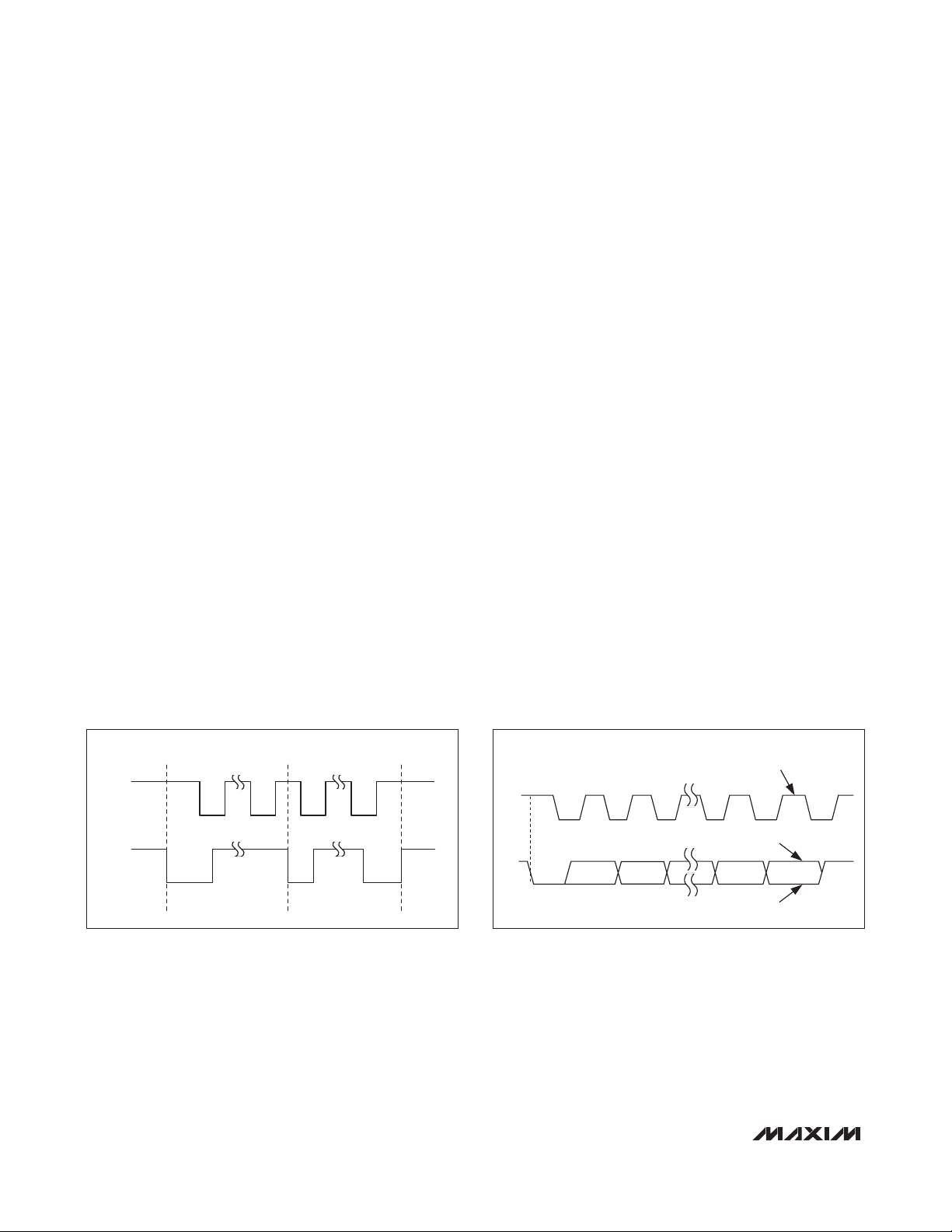
Bit Transfer
One data bit is transferred during each SCL cycle. The
data on SDA must remain stable during the high period
of the SCL pulse. Changes in SDA while SCL is high
are control signals (see the
START and STOP
Conditions
section).
START and STOP Conditions
SDA and SCL idle high when the bus is not in use. A
master initiates communication by issuing a START condition. A START condition is a high-to-low transition on
SDA with SCL high. A STOP condition is a low-to-high
transition on SDA while SCL is high (Figure 9). A START
condition from the master signals the beginning of a
transmission to the MAX9856. The master terminates
transmission, and frees the bus, by issuing a STOP condition. The bus remains active if a REPEATED START
condition is generated instead of a STOP condition.
Early STOP Conditions
The MAX9856 recognizes a STOP condition at any
point during data transmission except if the STOP condition occurs in the same high pulse as a START condition. For proper operation, do not send a STOP
condition during the same SCL high pulse as the
START condition.
Slave Address
The MAX9856 is preprogrammed with a slave address
of 0x20 or 0010000. The address is defined as the 7
most significant bits (MSBs) followed by the read/write
bit. Setting the read/write bit to 1 configures the
MAX9856 for read mode. Setting the read/write bit to 0
configures the MAX9856 for write mode. The address is
the first byte of information sent to the MAX9856 after
the START condition.
Acknowledge
The acknowledge bit (ACK) is a clocked 9th bit that the
MAX9856 uses to handshake receipt of each byte of
data when in write mode (see Figure 10). The MAX9856
pulls down SDA during the entire master-generated 9th
clock pulse if the previous byte is successfully
received. Monitoring ACK allows for detection of unsuccessful data transfers. An unsuccessful data transfer
occurs if a receiving device is busy or if a system fault
has occurred. In the event of an unsuccessful data
transfer, the bus master retries communication.
The master pulls down SDA during the 9th clock cycle to
acknowledge receipt of data when in read mode. An
acknowledge is sent by the master after each read byte
to allow data transfer to continue. A not acknowledge is
sent when the master reads the final byte of data from the
MAX9856, followed by a STOP condition.
MAX9856
Low-Power Audio CODEC with
DirectDrive Headphone Amplifiers
40 ______________________________________________________________________________________
Figure 9. START, STOP, and REPEATED START Conditions
Figure 10. Acknowledge
SSrP
SCL
SDA
START
CONDITION
SCL
SDA
1
289
NOT ACKNOWLEDGE
ACKNOWLEDGE
CLOCK PULSE FOR
ACKNOWLEDGMENT
Page 41
MAX9856
Low-Power Audio CODEC with
DirectDrive Headphone Amplifiers
______________________________________________________________________________________ 41
Figure 11. Writing 1 Byte of Data to the MAX9856
Figure 12. Writing n Bytes of Data to the MAX9856
Write Data Format
A write to the MAX9856 includes transmission of a
START condition, the slave address with the R/W bit set
to 0, 1 byte of data to configure the internal register
address pointer, 1 or more bytes of data, and a STOP
condition. Figure 11 illustrates the proper frame format
for writing 1 byte of data to the MAX9856. Figure 12
illustrates the frame format for writing n-bytes of data to
the MAX9856.
The slave address with the R/W bit set to 0 indicates
that the master intends to write data to the MAX9856.
The MAX9856 acknowledges receipt of the address
byte during the master-generated 9th SCL pulse.
The second byte transmitted from the master configures the MAX9856’s internal register address pointer.
The pointer tells the MAX9856 where to write the next
byte of data. An acknowledge pulse is sent by the
MAX9856 upon receipt of the address pointer data.
The third byte sent to the MAX9856 contains the data
that is written to the chosen register. An acknowledge
pulse from the MAX9856 signals receipt of the data
byte. The address pointer autoincrements to the next
register address after each received data byte. This
autoincrement feature allows a master to write to
sequential registers within one continuous frame. Figure
12 illustrates how to write to multiple registers with one
frame. The master signals the end of transmission by
issuing a STOP condition.
Register addresses greater than 0x1C are reserved. Do
not write to these addresses.
ACKNOWLEDGE FROM MAX9856
S AA
0SLAVE ADDRESS REGISTER ADDRESS DATA BYTE
R/W
ACKNOWLEDGE FROM MAX9856
ACKNOWLEDGE FROM MAX9856
B1 B0B3 B2B5 B4B7 B6
P
A
1 BYTE
ACKNOWLEDGE FROM MAX9856
S
SLAVE ADDRESS
R/W
ACKNOWLEDGE FROM MAX9856
A
REGISTER ADDRESS
ACKNOWLEDGE FROM MAX9856
A
DATA BYTE 1
1 BYTE
AUTOINCREMENT INTERNAL
REGISTER ADDRESS POINTER
AUTOINCREMENT INTERNAL
REGISTER ADDRESS POINTER
ACKNOWLEDGE FROM MAX9856
B1 B0B3 B2B5 B4B7 B6
A0
DATA BYTE n
1 BYTE
B1 B0B3 B2B5 B4B7 B6
A
P
Page 42

Read Data Format
Send the slave address with the R/W bit set to 1 to initiate a read operation. The MAX9856 acknowledges
receipt of its slave address by pulling SDA low during
the 9th SCL clock pulse. A START command followed
by a read command resets the address pointer to register 0x00. The first byte transmitted from the MAX9856
is the contents of register 0x00. Transmitted data is
valid on the rising edge of SCL. The address pointer
autoincrements after each read data byte. This autoincrement feature allows all registers to be read
sequentially within one continuous frame. A STOP condition can be issued after any number of read data
bytes. If a STOP condition is issued, followed by another read operation, the first data byte to be read is from
register 0x00.
The address pointer can be preset to a specific register
before a read command is issued. The master presets
the address pointer by first sending the MAX9856’s
slave address with the R/W bit set to 0 followed by the
register address. A REPEATED START condition is then
sent followed by the slave address with the R/W bit set
to 1. The MAX9856 then transmits the contents of the
specified register. The address pointer autoincrements
after transmitting the first byte. The master acknowledges receipt of each read byte during the acknowledge clock pulse. The master must acknowledge all
correctly received bytes except the last byte. The final
byte must be followed by a not acknowledge from the
master and then a STOP condition. Figure 13 illustrates
the frame format for reading 1 byte from the MAX9856.
Figure 14 illustrates the frame format for reading multiple bytes from the MAX9856.
MAX9856
Low-Power Audio CODEC with
DirectDrive Headphone Amplifiers
42 ______________________________________________________________________________________
Figure 13. Reading 1 Indexed Byte of Data from the MAX9856
Figure 14. Reading n Bytes of Indexed Data from the MAX9856
ACKNOWLEDGE FROM MAX9856
SA
R/W
ACKNOWLEDGE FROM MAX9856
0
REPEATED START
ACKNOWLEDGE FROM MAX9856
Sr 1SLAVE ADDRESS REGISTER ADDRESS SLAVE ADDRESS DATA BYTE
NOT ACKNOWLEDGE FROM MASTER
AA
R/W
A
1 BYTE
AUTOINCREMENT INTERNAL
REGISTER ADDRESS POINTER
P
ACKNOWLEDGE FROM MAX9856
SA
R/W
ACKNOWLEDGE FROM MAX9856
0
REPEATED START
ACKNOWLEDGE FROM MAX9856
Sr 1SLAVE ADDRESS REGISTER ADDRESS SLAVE ADDRESS DATA BYTE
R/W
AA
1 BYTE
A
AUTOINCREMENT INTERNAL
REGISTER ADDRESS POINTER
Page 43

PCB Layout and Bypassing
Proper layout and grounding are essential for optimum
performance. Use large traces for the power-supply
inputs and amplifier outputs to minimize losses due to
parasitic trace resistance. Proper grounding improves
audio performance, minimizes crosstalk between channels, and prevents any switching noise from coupling
into the audio signal. Connect AGND, DGND, CPGND,
and PGND together at a single point on the PCB using
the star grounding technique. Route DGND, CPGND,
and all traces that carry switching transients or digital
signals separately from AGND and the analog audio
signal paths. Ground all components associated with
the charge pump to CPGND (CPVSS bypassing and
CPVDD bypassing). Connect all digital I/O termination
to DGND including DVDD and DVDDS2 bypassing.
Bypass REF and MICBIAS to AGND.
Connect PVSS and SVSS together at the device and
place the charge-pump hold capacitor (C2) as close to
SVSS as possible and ground to CPGND. Bypass
CPVDD with a 1µF capacitor to CPGND and place the
bypass capacitor as close to the device as possible.
The MAX9856 thin QFN package features an exposed
thermal pad on its underside. This pad lowers the package’s thermal resistance by providing a direct heat
conduction path from the die to the PCB. Connect the
exposed thermal pad to AGND.
An evaluation kit (EV Kit) is available to provide an
example layout for the MAX9856. The EV Kit allows
quick setup of the MAX9856 and includes easy-to-use
software allowing all internal registers to be controlled.
MAX9856
Low-Power Audio CODEC with
DirectDrive Headphone Amplifiers
______________________________________________________________________________________ 43
Chip Information
PROCESS: BiCMOS
Pin Configuration
TOP VIEW
31
DVDD
32
DGND
33
INLN
34
INLP
35
MICL
36
MICGND
37
MICR
38
MICBIAS
39
AGND
40
JACKSNS
* EP = EXPOSED PAD.
LRCLK_A
MCLK
+
12
LINEIN2
LINEIN1
SDIN
SDOUT
25
BCLK
DVDDS2
27282930 26 24 23 22
MAX9856
4567
3
PREG
NREG
AUXIN
MBIAS
THIN QFN
(6mm x 6mm)
LRCLK_D
IRQ
*EP
8910
REF
LGNDSNS
SDA
LOUTL
SCL
21
LOUTR
20
19
18
17
16
15
14
13
12
11
CPVDD
C1P
CPGND
C1N
PVSS
SVSS
HPR
HPL
AVDD
HGNDSNS
Page 44
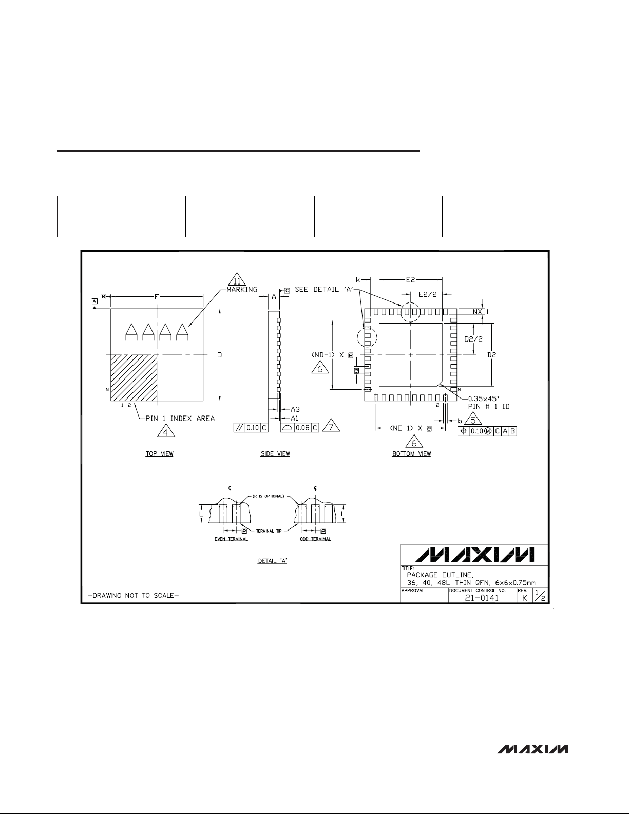
MAX9856
Low-Power Audio CODEC with
DirectDrive Headphone Amplifiers
44 ______________________________________________________________________________________
Package Information
For the latest package outline information and land patterns (footprints), go to www.maxim-ic.com/packages. Note that a "+", "#", or
"-" in the package code indicates RoHS status only. Package drawings may show a different suffix character, but the drawing pertains to the package regardless of RoHS status.
PACKAGE TYPE PACKAGE CODE OUTLINE NO.
40 TQFN T4066+5 21-0141 90-0055
LAND
PATTERN NO.
Page 45
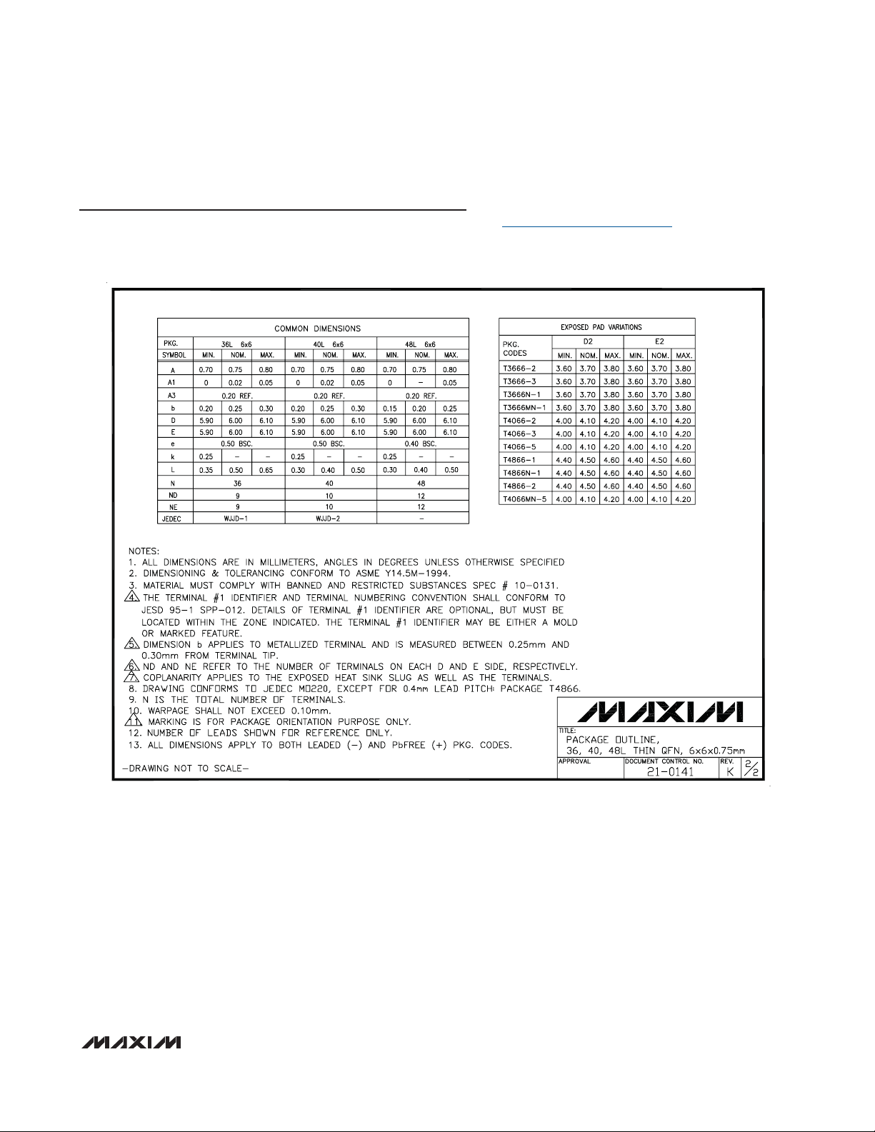
MAX9856
Low-Power Audio CODEC with
DirectDrive Headphone Amplifiers
______________________________________________________________________________________ 45
Package Information (continued)
For the latest package outline information and land patterns (footprints), go to www.maxim-ic.com/packages. Note that a "+", "#", or
"-" in the package code indicates RoHS status only. Package drawings may show a different suffix character, but the drawing pertains to the package regardless of RoHS status.
Page 46

MAX9856
Low-Power Audio CODEC with
DirectDrive Headphone Amplifiers
Maxim cannot assume responsibility for use of any circuitry other than circuitry entirely embodied in a Maxim product. No circuit patent licenses are
implied. Maxim reserves the right to change the circuitry and specifications without notice at any time. The parametric values (min and max limits) shown in
the Electrical Characteristics table are guaranteed. Other parametric values quoted in this data sheet are provided for guidance.
46
____________________Maxim Integrated Products, 120 San Gabriel Drive, Sunnyvale, CA 94086 408-737-7600
© 2011 Maxim Integrated Products Maxim is a registered trademark of Maxim Integrated Products, Inc.
Revision History
REVISION
NUMBER
0 3/08 Initial release —
1 9/08 Added new Note 1 to EC table 2–10
2 12/11 Added automotive qualified part information to data sheet 1, 2
REVISION
DATE
DESCRIPTION
PAGES
CHANGED
 Loading...