

E V A L UA T I ON K IT A V AI L A BL E
19-5912; Rev 0; 6/11
MAX98309/MAX98310
Mono 1.4W Class AB Audio Amplifiers
General Description
The MAX98309/MAX98310 mono 1.4W class AB audio
amplifiers offer low quiescent current while maintaining
excellent SNR and low 0.008% THD+N. These ICs feature excellent 90dB PSRR and state of the art click-andpop suppression.
The ICs are offered with an internally fixed 0dB, 3dB,
6dB, and 9dB gain (MAX98310) or an externally set gain
(MAX98309) through external resistors.
The MAX98309 feature a 10ms or 100ms pin-selectable
turn-on time, while the MAX98310 has a preset 5ms turnon time.
The MAX98309/MAX98310 are available in a (1.0mm x
1.0mm) 9-bump, 0.3mm pitch WLP, and are specified over
the extended -40NC to +85NC temperature range.
Applications
Cell Phones/Smartphones
Digital Cameras
GPS
Portable Media Players
e-Readers
Tablets
Benefits and Features
S Enhances System Performance
Differential Input Improves Noise Immunity
Industry-Leading Click-and-Pop Suppression
High 90dB PSRR (fIN = 217Hz)
S Smaller Solution Size
1mm x 1mm WLP Footprint
S Extends Battery Life
Low Quiescent Current
S Delivers Robust System Design
Thermal Overload Protection
Short-Circuit Protection
S 1.2mA Supply Current (VDD = 3.7V)
S 750mW into 8I (VDD = 3.7V)
S 2.5V to 5.5V Supply Operation
S Pin-Selectable, Internally-Fixed Gain (MAX98310)
S 1.8V Logic-Compatible SHDN Input
Ordering Information appears at end of data sheet.
For related parts and recommended products to use with this part,
refer to www.maxim-ic.com/MAX98309.related.
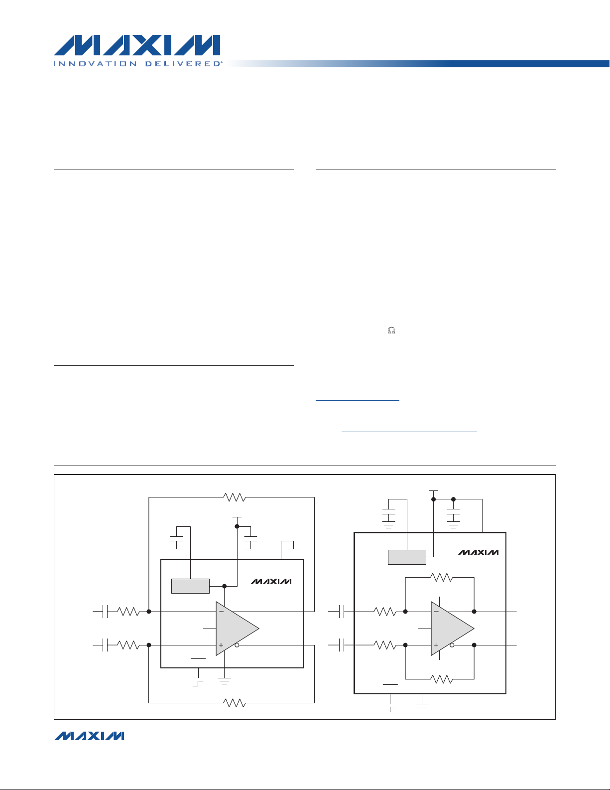
Simplified Block Diagram
BIAS V
BIAS
BIAS
2.5V TO 5.5V
DD
R
V
DD
R
F
GND
F
GAIN
MAX98310
OUT+
OUT-
R
F
2.5V TO 5.5V
0.1µF 1µF
GND
R
V
DD
MAX98309
OUT+
OUT-
F
BIAS TON
BIAS
C
IN
R
IN
C
IN
R
IN
IN-
BIAS
IN+
SHDN
0.1µF 1µF
C
IN
C
IN
IN-
IN+
R
IN
R
IN
SHDN GND
����������������������������������������������������������������� Maxim Integrated Products 1
For pricing, delivery, and ordering information, please contact Maxim Direct at 1-888-629-4642,
or visit Maxim’s website at www.maxim-ic.com.
MAX98309/MAX98310
Mono 1.4W Class AB Audio Amplifiers
ABSOLUTE MAXIMUM RATINGS
VDD to GND ............................................................... -0.3V to 6V
SHDN to GND ........................................................... -0.3V to 6V
All Other Pins to GND ...............................-0.3V to (V
Continuous Current
VDD, GND, OUT_ ....................................................... Q750mA
IN_, SHDN, BIAS, GAIN, TON ......................................... Q20mA
OUT_ Short Circuit to GND or VDD Duration ............Continuous
Stresses beyond those listed under “Absolute Maximum Ratings” may cause permanent damage to the device. These are stress ratings only, and functional operation of the device at these or any other conditions beyond those indicated in the operational sections of the specifications is not implied. Exposure to absolute
maximum rating conditions for extended periods may affect device reliability.
DD
+ 0.3V)
PACKAGE THERMAL CHARACTERISTICS (Note 1)
WLP
Junction-to-Ambient Thermal Resistance (BJA)......... 94°C/W
Junction-to-Case Thermal Resistance (BJC) ...............41°C/W
Note 1: Package thermal resistances were obtained using the method described in JEDEC specification JESD51-7, using a four-
layer board. For detailed information on package thermal considerations, refer to www.maxim-ic.com/thermal-tutorial.
OUT+ to OUT- Short Circuit Duration .......................Continuous
Continuous Power Dissipation (TA = +70NC)
WLP (derate 11.9mW/NC above +70NC)......................848mW
Junction Temperature .....................................................+150NC
Operating Temperature Range .......................... -40NC to +85NC
Storage Temperature Range ............................ -65NC to +150NC
Soldering Temperature (reflow).......................................+260NC
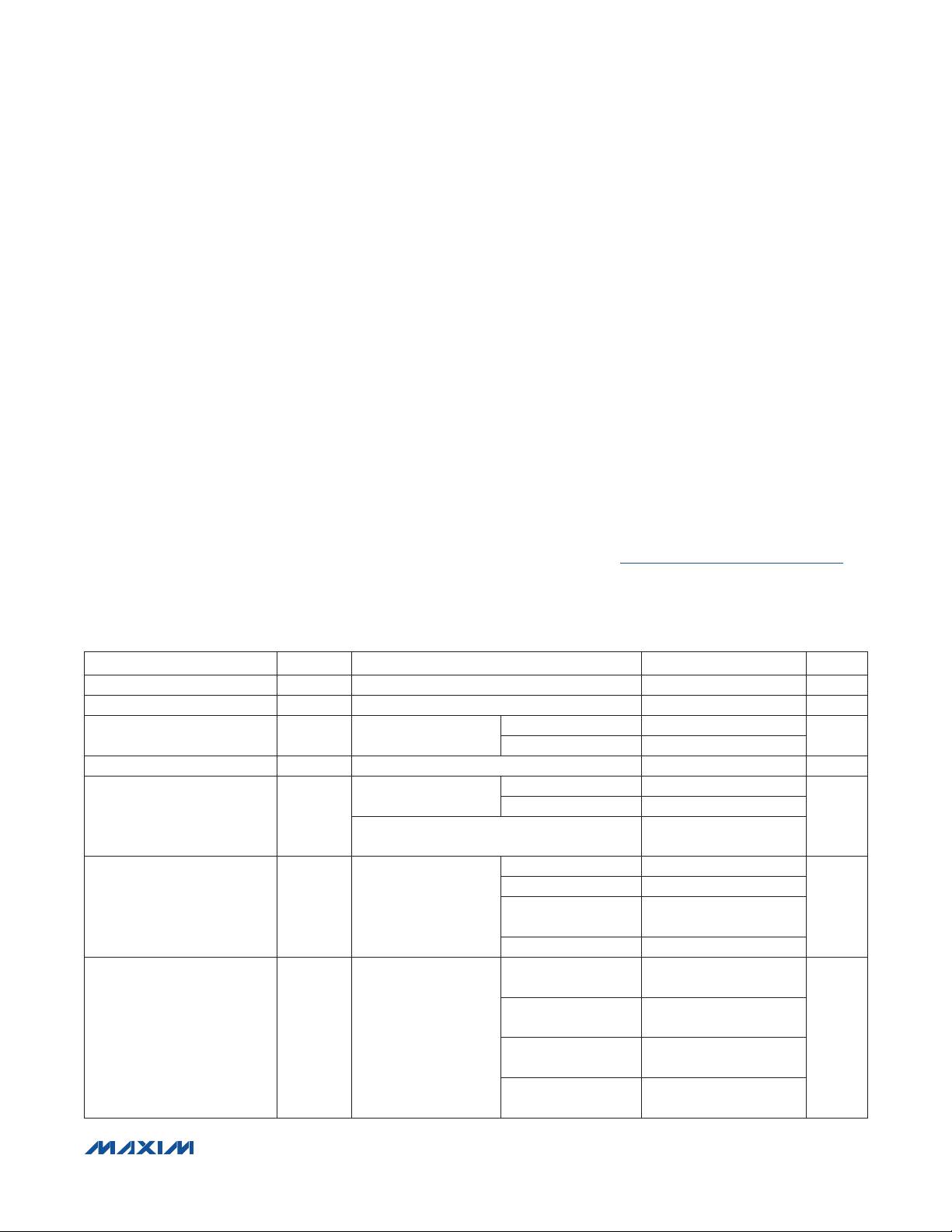
ELECTRICAL CHARACTERISTICS
(VDD = 3.7V, V
TA = T
MIN to TMAX.
PARAMETER SYMBOL CONDITIONS MIN TYP MAX UNITS
Supply Voltage Range V
Undervoltage Lockout UVLO VDD falling 1.8 2.3 V
Quiescent Supply Current I
Shutdown Supply Current I
Turn-On Time t
Gain A
Gain Selection Threshold MAX98310
= 0V, SHDN = VDD, GAIN = VDD (0dB), C
GND
Typical values are at TA = +25°C, unless otherwise noted.) (Note 2)
DD
VDD
VDD_SD
ON
Guaranteed by PSRR test 2.5 5.5 V
SHDN = V
V
SHDN
MAX98309 shutdown to
full operation
MAX98310 shutdown to full operation 5.7 11.5
MAX98310
V
DD
= 0V, TA = +25NC
= 0.1µF, C
BIAS
V
= 3.7V 1.2
DD
V
= 5V 1.9 1.8
DD
TON = GND 10 22.8
TON = V
GAIN = V
GAIN = GND 2.75 3 3.25
GAIN = unconnected 5.75 6 6.25
GAIN = BIAS 8.75 9 9.25
GAIN = V
GAIN = GND
GAIN = unconnected
GAIN = BIAS
= 0.47µF, no load: RIN = RF = 10kI (MAX98309),
IN
2 3
DD
DD
DD
-0.25 0 +0.25
0.80 x
V
DD
0.16 x
V
DD
0.35 x
V
DD
100
0.05 x
V
DD
0.24 x
V
DD
0.69 x
V
DD
mA
FA
ms
dB
V
����������������������������������������������������������������� Maxim Integrated Products 2
Mono 1.4W Class AB Audio Amplifiers
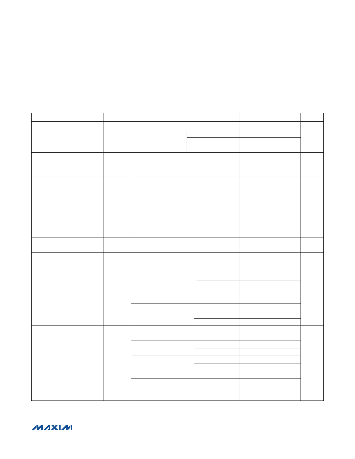
ELECTRICAL CHARACTERISTICS (continued)
(VDD = 3.7V, V
= T
MIN to TMAX.
PARAMETER SYMBOL CONDITIONS MIN TYP MAX UNITS
Differential Input Resistance R
Input Bias Current I
Shutdown Input Bias Current
Output Offset Voltage
= 0V, SHDN = VDD, GAIN = VDD (0dB), C
GND
Typical values are at TA = +25°C, unless otherwise noted.) (Note 2)
MAX98309, SHDN = VDD
INDIFF
INBIAS
I
INBIAS_
SHDN
V
OS
MAX98310
MAX98309/MAX98310, SHDN = V
SHDN = GND, IN_ = VDD or IN_ = GND
TA = +25NC (Note 3) Q0.2 Q1
= 0.1µF, C
BIAS
MAX98309/MAX98310
= 0.47µF, no load: RIN = RF = 10kI (MAX98309), TA
IN
1000
GAIN = 0dB 38.2
GAIN = 3dB 31.7
GAIN = 6dB 25.5
DD
-5 +5
Q1 FA
kI
FA
mV
RL = 8I, 32 samples per
Click-and-Pop Level K
Common-Mode Bias Voltage V
Input Common-Mode Voltage
Range
Common-Mode Rejection Ratio CMRR MAX98310/MAX98310
Power-Supply Rejection Ratio PSRR
Output Power P
BIAS
V
OUT
CP
CM
second, A-weighted,
TA = +25NC (Notes 3, 4)
Voltage at BIAS
Inferred from CMRR test 0.5
DC 2.5V to 5.5V 73 93
V
= 200mV
RIPPLE
(Note 3)
VDD = 3.7V, 1% THD+N
V
= 3.7V, 10% THD+N
DD
V
= 5V, 1% THD+N
DD
(Note 5)
VDD = 5V, 10% THD+N
(Note 5)
P-P
Into shutdown -66
Out of shutdown -66
0.475
x V
Guaranteed over
input commonmode voltage
range
fIN = 1kHz,
RL = 8I + 33FH
fIN = 217Hz 90
fIN = 1kHz 90
fIN = 10kHz 72
RL = 8I + 68FH
RL = 4I + 33FH
RL = 8I + 68FH
RL = 4I + 33FH
RL = 8I + 68FH
RL = 4I + 33FH,
thermally limited
RL = 8I + 68FH
RL = 4I + 33FH,
thermally limited
-50 -76
DD
0.5 x
V
-62
0.750
1.2
0.9
1.5
1.4
2.1
1.7
2.7
DD
0.525
x V
DD
VDD -
0.6
dBV
V
V
dB
dB
W
����������������������������������������������������������������� Maxim Integrated Products 3
MAX98309/MAX98310
Mono 1.4W Class AB Audio Amplifiers
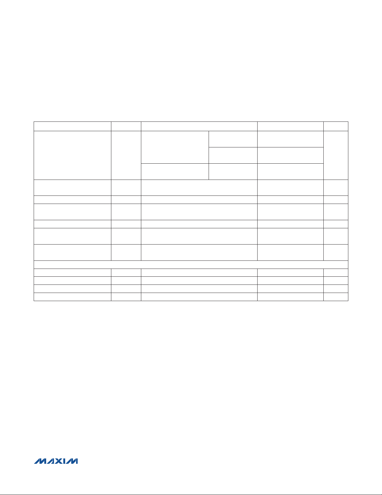
ELECTRICAL CHARACTERISTICS (continued)
(VDD = 3.7V, V
TA = T
MIN to TMAX.
PARAMETER SYMBOL CONDITIONS MIN TYP MAX UNITS
Total Harmonic Distortion Plus
Noise
Signal-to-Noise Ratio SNR
Output Noise Voltage V
Overcurrent Protection
Threshold
Thermal-Protection Threshold +160
= 0V, SH DN = VDD, GAIN = VDD (0dB), C
GND
Typical values are at TA = +25°C, unless otherwise noted.) (Note 2)
fIN = 1kHz, BW = 22Hz to
THD+N
22kHz
fIN = 6kHz, BW = 22Hz to
22kHz
A-weighted, VDD = 5V, P
RL = 8I + 33FH
A-weighted (Note 3) 9
N
= 0.1µF, C
BIAS
RL = 8I + 68FH,
P
RL = 4I + 33FH,
P
RL = 8I + 68FH,
P
= 1.4W,
OUT
= 0.47µF, no load: RIN = RF = 10kI (MAX98309),
IN
= 375mW
OUT
= 750mW
OUT
= 375mW
OUT
0.06 0.02
0.008
0.01
110 dB
%
FV
2 A
NC
Thermal-Protection Hysteresis 15
Maximum Capacitive Load
Drive
LOGIC INPUT (SHDN, TON) (MAX98309)
Input Logic-High V
Input Logic-Low V
Input Leakage Current High I
Input Leakage Current Low I
Note 2: All specifications are 100% tested at TA = +25°C; temperature limits are guaranteed by design.
Note 3: Inputs AC-coupled to GND.
Note 4: Mode transitions controlled by SHDN.
Note 5: Thermally limited by package.
C
IH
Bridge-tied load capacitance 500 pF
L
1.8V logic compliant 1.4 V
IH
1.8V logic compliant 0.4 V
IL
TA = +25NC
TA = +25NC
IL
NC
1
1
FA
FA
����������������������������������������������������������������� Maxim Integrated Products 4
MAX98309/MAX98310
Mono 1.4W Class AB Audio Amplifiers
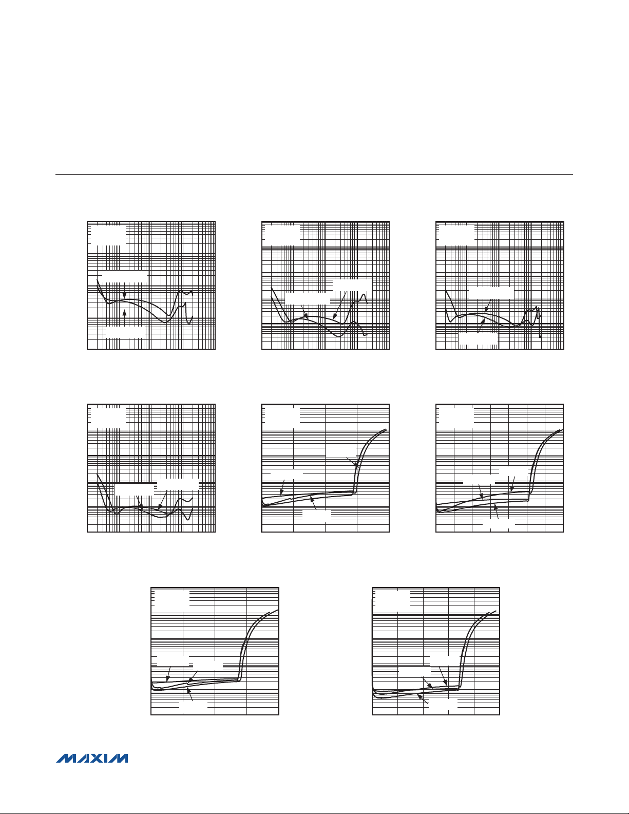
Typical Operating Characteristics
(VDD = 3.7V, V
= 0V, SHDN = VDD, GAIN = GND (RF = RIN = 10kI), C
GND
TOTAL HARMONIC DISTORTION PLUS
NOISE vs. FREQUENCY
10
VDD = 4.2V
R
= 4I
L
1
P
= 300mW
0.1
THD+N (%)
0.01
0.001
OUT
P
= 50mW
OUT
10 100k
FREQUENCY (kHz)
TOTAL HARMONIC DISTORTION PLUS
NOISE vs. FREQUENCY
100
VDD = 3.7V
= 8I
R
L
10
1
THD+N (%)
0.1
0.01
0.001
10 100k
P
= 50mW
OUT
FREQUENCY (Hz)
TOTAL HARMONIC DISTORTION PLUS
100
10
MAX98309 toc01
10k1k100
MAX98309 toc04
P
= 500mW
OUT
10k1k100
NOISE vs. OUTPUT POWER
VDD = 3.7V
R
= 4I
L
BIAS
TOTAL HARMONIC DISTORTION PLUS
NOISE vs. FREQUENCY
100
VDD = 5V
RL = 8I
10
1
P
THD+N (%)
0.1
0.01
0.001
P
= 200mW
OUT
10 100k
FREQUENCY (Hz)
OUT
TOTAL HARMONIC DISTORTION PLUS
NOISE vs. OUTPUT POWER
100
VDD = 4.2V
R
= 4I
L
10
1
THD+N (%)
0.001
fIN = 300Hz
0.1
0.01
0 2000
OUTPUT POWER (mW)
MAX98309 toc07
fIN = 6kHz
fIN = 1kHz
= 0.1µF, CIN = 1µF, no load, unless otherwise noted.)
TOTAL HARMONIC DISTORTION PLUS
NOISE vs. FREQUENCY
100
VDD = 3.7V
MAX98309 toc02
= 1.2W
10k1k100
RL = 4I
10
1
P
= 800mW
THD+N (%)
0.1
0.01
0.001
10 100k
OUT
P
= 50mW
OUT
FREQUENCY (Hz)
10k1k100
TOTAL HARMONIC DISTORTION PLUS
NOISE vs. OUTPUT POWER
100
VDD = 5V
R
= 8I
MAX98309 toc05
THD+N (%)
0.001
15001000500
L
10
1
0.1
0.01
fIN = 300Hz
0 1750
OUTPUT POWER (mW)
fIN = 6kHz
fIN = 1kHz
150012501000750500250
TOTAL HARMONIC DISTORTION PLUS
NOISE vs. OUTPUT POWER
100
VDD = 3.7V
RL = 8I
10
MAX98309 toc08
MAX98309 toc03
MAX98309 toc06
1
fIN = 300Hz
THD+N (%)
0.1
0.01
0.001
0 1600
fIN = 6kHz
fIN = 1kHz
OUTPUT POWER (mW)
1200800400
1
THD+N (%)
0.1
0.01
0.001
fIN = 300Hz
0 1000
fIN = 6kHz
fIN = 1kHz
OUTPUT POWER (mW)
800600400200
����������������������������������������������������������������� Maxim Integrated Products 5

MAX98309/MAX98310
Mono 1.4W Class AB Audio Amplifiers
Typical Operating Characteristics (continued)
(VDD = 3.7V, V
= 0V, SHDN = VDD, GAIN = GND (RF = RIN = 10kI), C
GND
OFFSET VOLTAGE
vs. COMMON-MODE VOLTAGE
5
4
3
2
1
(mV)
0
OS
V
-1
-2
-3
-4
-5
0 5
COMMON-MODE VOLTAGE (V)
VDD = 5V
RL = 8
4321
I
MAX98309 toc09
OUTPUT POWER vs. SUPPLY VOLTAGE
2500
fIN = 1kHz
RL = 8I
2000
1500
1000
OUTPUT POWER (mW)
500
THD+N = 10%
THD+N = 10%
MAX98309 toc11
= 0.1µF, CIN = 1µF, no load, unless otherwise noted.)
BIAS
OFFSET VOLTAGE
vs. COMMON-MODE VOLTAGE
4
3
2
1
(mV)
0
OS
V
-1
-2
-3
-4
0 3.5
COMMON-MODE VOLTAGE (V)
VDD = 3.7V
RL = 8I
3.02.50.5 1.0 1.5 2.0
MAX98309 toc10
OUTPUT POWER vs. SUPPLY VOLTAGE
3500
fIN = 1kHz
= 4I
R
500
L
THD+N = 10%
MAX98309 toc12
THERMALLY
LIMITED
THD+N = 1%
3000
2500
2000
1500
OUTPUT POWER (mW)
1000
0
2.5 5.5
SUPPLY VOLATGE (V)
OUTPUT POWER vs. LOAD
3.0
2.5
2.0
1.5
1.0
OUTPUT POWER (W)
0.5
0
LOAD RESISTANCE (I)
Z
LOAD
THERMALLY
LIMITED
THD+N = 10%
THD+N = 1%
100101 1k
5.04.54.03.53.0
VDD = 5V
= 1kHz
f
IN
= LOAD + 68µH
MAX98309 toc13
0
2.5 5.5
SUPPLY VOLATGE (V)
OUTPUT POWER vs. LOAD
1.8
1.6
1.4
1.2
1.0
0.8
0.6
OUTPUT POWER (mW)
0.4
THD+N = 1%
0.2
0
1 1k
LOAD RESISTANCE (I)
Z
LOAD
THD+N = 10%
= LOAD + 68µH
10010
5.04.54.03.53.0
VDD = 3.7V
= 1kHz
f
IN
����������������������������������������������������������������� Maxim Integrated Products 6
MAX98309 toc14

MAX98309/MAX98310
Mono 1.4W Class AB Audio Amplifiers
Typical Operating Characteristics (continued)
(VDD = 3.7V, V
= 0V, SHDN = VDD, GAIN = GND (RF = RIN = 10kI), C
GND
POWER DISSIPATION
vs. OUTPUT POWER
1400
1200
1000
800
600
400
POWER DISSIPATION (mW)
200
0
0 2000
RL = 4I
OUTPUT POWER (mW)
0
RL = 8I
-10
V
RIPPLE
-20
-30
-40
-50
-60
-70
PSRR (dB)
-80
-90
-100
-110
-120
-130
-140
10 100k
0
RL = 8I
-10
THD + N = 1%
-20
-30
-40
-50
CMRR (dB)
-60
-70
-80
-90
-100
10 100k
VDD = 5V
= 1kHz
f
= P
RL = 8I
OUTL
15001000500
IN
+ P
OUTR
P
OUT
PSRR vs. FREQUENCY
(MAX98309)
= 200mV
VDD = 5V
VDD = 3.7V
FREQUENCY (Hz)
CMRR vs. FREQUENCY
(MAX98309)
VDD = 3.7V
VDD = 5V
FREQUENCY (Hz)
800
700
MAX98309 toc15
600
500
400
300
POWER DISSIPATION (mW)
200
100
0
0 1500
10k1k100
10k1k100
POWER DISSIPATION
vs. OUTPUT POWER
RL = 8I
OUTPUT POWER (mW)
MAX98309 toc18
MAX98309 toc20
RL = 4I
P
OUT
= 0.1µF, CIN = 1µF, no load, unless otherwise noted.)
BIAS
GAIN vs. FREQUENCY
(MAX98310)
12
11
= P
VDD = 3.7V
fIN = 1kHz
OUTL
1200900300 600
+ P
OUTR
MAX98309 toc16
10
9
8
7
6
5
4
3
GAIN (dB)
2
1
0
-1
-2
-3
-4
-5
10 100k 1000k
AV = 9dB
AV = 6dB
AV = 3dB
AV = 0dB
10k1k100
FREQUENCY (Hz)
PSRR vs. FREQUENCY
(MAX98310)
0
RL = 8I
-10
V
= 200mV
RIPPLE
-20
-30
-40
-50
-60
PSRR (dB)
-70
-80
-90
-100
-110
-120
10 100k
VDD = 3.7V
VDD = 5V
10k1k100
FREQUENCY (Hz)
CMRR vs. FREQUENCY
(MAX98310)
0
RL = 8I
-10
THD + N = 1%
-20
-30
-40
-50
CMRR (dB)
-60
-70
-80
-90
-100
10 100k
VDD = 3.7V
VDD = 5V
10k1k100
FREQUENCY (Hz)
MAX98309 toc17
MAX98309 toc19
MAX98309 toc21
����������������������������������������������������������������� Maxim Integrated Products 7

MAX98309/MAX98310
Mono 1.4W Class AB Audio Amplifiers
Typical Operating Characteristics (continued)
(VDD = 3.7V, V
= 0V, SHDN = VDD, GAIN = GND (RF = RIN = 10kI), C
GND
TURN-ON TIME (MAX98309) 10ms
2ms/div
3.0
2.5
2.0
1.5
1.0
SUPPLY CURRENT (mA)
0.5
MAX98309 toc22
SUPPLY CURRENT
vs. SUPPLY VOLTAGE
= 0.1µF, CIN = 1µF, no load, unless otherwise noted.)
BIAS
TURN-ON TIME (MAX98309) 100ms
20ms/div
MAX98309 toc25
MAX98309 toc23
TURN-ON TIME MAX98310
SUPPLY CURRENT vs. TEMPERATURE
2.5
2.0
1.5
1.0
SUPPLY CURRENT (mA)
0.5
VDD = 5V
VDD = 3.7V
MAX98309 toc24
1ms/div
MAX98309 toc26
0
2.5 5.5
SUPPLY VOLTAGE (V)
SHUTDOWN CURRENT
vs. SUPPLY VOLTAGE
9
8
7
6
5
4
3
SHUTDOWN CURRENT (µA)
2
1
0
2.5 5.5
SUPPLY VOLTAGE (V)
5.04.54.03.53.0
MAX98309 toc27
5.04.54.03.53.0
0
-40 85
TEMPERATURE (°C)
SHUTDOWN CURRENT
vs. TEMPERATURE
10
9
8
7
6
5
4
3
SHUTDOWN CURRENT (µA)
2
1
0
-40 85
VDD = 5V
VDD = 3.7V
TEMPERATURE (°C)
603510-15
MAX98309 toc28
603510-15
����������������������������������������������������������������� Maxim Integrated Products 8

MAX98309/MAX98310
Mono 1.4W Class AB Audio Amplifiers
Pin Configurations
TOP VIEW
(BUMP SIDE DOWN)
A
B
C
MAX98309
1
+
OUT+ SHDN
GND
OUT- BIAS
2 3
TON V
IN-
DD
IN+
TOP VIEW
(BUMP SIDE DOWN)
A
B
C
WLP
PIN
MAX98309 MAX98310
NAME FUNCTION
A1 A1 OUT+ Amplifier Positive Output
A2 A2
SHDN
Active-Low Shutdown Input. Connect to GND to place the IC into shutdown. Connect
to VDD for normal operation.
A3 A3 IN- Inverting Audio Input
B1 B1 GND Ground
B2 — TON
Turn-On Time Selection. Connect TON to GND for a 10ms turn-on time. Connect TON
to VDD for a 100ms turn on time.
— B2 GAIN Gain Select Input. See Table 1 for gain settings.
B3 B3 V
DD
Power Supply Input. Connect a 1FF capacitor from VDD to GND.
C1 C1 OUT- Amplifier Negative Output
C2 C2 BIAS
Common-Mode DC Bias Bypass. Connect a 0.1FF (min) capacitor to GND.
C3 C3 IN+ Noninverting Audio Input
MAX98310
1
+
OUT+ SHDN
GND
OUT- BIAS
2 3
GAIN V
WLP
IN-
DD
IN+
Pin Descriptions
����������������������������������������������������������������� Maxim Integrated Products 9

MAX98309/MAX98310
V
Mono 1.4W Class AB Audio Amplifiers
Detailed Description
The MAX98309/MAX98310 mono 1.4W Class AB audio
amplifiers offer low quiescent current while maintaining
excellent SNR and low 0.008% THD+N. Both ICs feature
excellent 90dB PSRR and state-of-the-art click-and-pop
suppression.
The ICs are offered with an internally fixed 0dB, 3dB,
6dB, and 9dB gain (MAX98310) or an externally set gain
(MAX98309) through external resistors.
The MAX98309 features a 10ms or 100ms pin-selectable
turn-on time, while the MAX98310 has a preset 5ms turnon time.
Bias
The ICs operate from a single 2.5V to 5.5V power supply
and feature an internally generated common-mode bias
voltage of VDD/2 reference to ground. BIAS provides both
click-and-pop suppression and sets the DC bias level
for the audio outputs. Choose the value of the bypass
capacitor as described in the BIAS Capacitor section. Do
not connect external loads to BIAS as this can affect the
overall performance.
Turn-On Time
The MAX98309 external gain amplifier features a selectable turn-on time for optimized click-and-pop performance. Connect TON to GND for a 10ms turn-on time.
Connect TON to VDD for a 100ms turn-on time. The
MAX98310 has a preset 5ms turn-on time.
Shutdown Mode
The ICs feature a 1.8FA low-power shutdown mode
that reduces quiescent current consumption. When the
active-low shutdown mode is entered, the ICs’ internal
bias circuitry is disabled, the amplifier outputs go high
impedance, and BIAS is driven to GND.
Click-and-Pop Suppression
The ICs feature Maxim’s industry-leading click-andpop suppression circuitry. During startup, the amplifier
common-mode bias voltage ramps to the DC bias point.
When entering shutdown, the amplifier outputs are high
impedance between both outputs. This scheme minimizes the energy present in the audio band.
Applications Information
BTL Amplifier
The ICs are designed to drive a load differentially, a
configuration referred to as bridge-tied load, or BTL. The
BTL configuration (Figure 1) offers advantages over the
single-ended configuration, where one side of the load
is connected to ground. Driving the load differentially
doubles the output voltage compared to a single-ended
amplifier under similar conditions.
Substituting 2 x V
OUT(P-P)
equations yields four times the output power due to
doubling of the output voltage:
P
Because the differential outputs are biased at midsupply,
there is no net DC voltage across the load. This eliminates the need for DC-blocking capacitors required for
single-ended amplifiers. These capacitors can be large,
expensive, consume board space, and degrade lowfrequency performance.
Power Dissipation and Heatsinking
Under normal operating conditions, the ICs dissipate a
significant amount of power. The maximum power dissipation is given in the Absolute Maximum Ratings or can
be calculated by the following equation:
D(MAX)
where T
is +150NC, TA is the ambient temperature,
J(MAX)
and BJA is the reciprocal of the derating factor in C/W as
specified in the Absolute Maximum Ratings.
V
RMS
OUT
for V
=
=
=
+1
-1
OUT(P-P)
OUT (P P)
−
2 2
V 2
RMS
R
L
T TP−
J(MAX) A
θ
JA
into the following
V
OUT(P-P)
2 x V
OUT(P-P)
V
OUT(P-P)
Figure 1. BTL Configuration
���������������������������������������������������������������� Maxim Integrated Products 10

MAX98309/MAX98310
Mono 1.4W Class AB Audio Amplifiers
The increase in power delivered by the BTL configuration
directly results in an increase in internal power dissipation over the single-ended configuration. The maximum
internal power dissipation for a given VDD and load is
given by the following equation:
2
2V
P
D(MAX)
DD
2
R=π
L
If the internal power dissipation for a given application
exceeds the maximum allowed for a given package,
reduce power dissipation by increasing the ground plane
heatsinking capability and the size of the traces to the
device. See the Layout and Grounding section. Other
methods for reducing power dissipation are to reduce
VDD, increase load impedance, decrease ambient
temperature, reduce gain, or reduce input signal.
Thermal-overload protection limits total power dissipation
in the MAX98309/MAX98310. When the junction temperature exceeds +160NC, the thermal protection circuitry
disables the amplifier. Operation returns to normal once
the die cools by 15NC.
Amplifier Gain
Fixed Differential Gain (MAX98310)
The MAX98310 features four internally fixed differential
gain options selectable by GAIN (Table 1). This simplifies
design, decreases required application footprint size, and
eliminates external gain-setting resistors.
External Differential Gain (MAX98309)
The MAX98309 features an external gain option. Resistors
RF and RIN. See the Simplified Block Diagram and set the
gain of the amplifier as follows:
R
AR=
F
V
IN
where AV is the desired voltage gain. Hence, an RIN of
10kI and an RF of 20kI yields a gain of 2V/V or 6dB.
RF can be either fixed or variable, allowing the use of a
digitally controlled potentiometer to alter the gain under
software control.
Table 1. Fixed Differential Gain
GAIN CONNECTION GAIN (dB)
V
DD
GND 3
Unconnected 6
BIAS 9
0
Input Filter
The fully differential amplifier inputs can be biased at
voltages other than midsupply. The common-mode
feedback circuit adjusts for input bias, ensuring the outputs are still biased at midsupply. Input capacitors are
not required as long as the input voltage is within the
specified common-mode range listed in the Electrical
Characteristics table.
If input capacitors are used, input capacitor CIN, in conjunction with the input resistor RIN, forms a highpass filter
that removes the DC bias from an incoming signal. The
AC-coupling capacitor allows the amplifier to bias the signal to an optimum DC level. Assuming zero-source impedance, the -3dB point of the highpass filter is given by:
=
2 R C
π
1
IN IN
Setting f
f
3dB
−
too high affects the low-frequency response
-3dB
of the amplifier. Use capacitors with adequately low voltage coefficients, such as X7R ceramic capacitors with a
high voltage rating. Capacitors with higher voltage coefficients result in increased distortion at low frequencies.
BIAS Capacitor
BIAS is the output of the internally generated VDD/2 bias
voltage. The BIAS bypass capacitor, C
, improves
BIAS
PSRR and THD+N by reducing power supply and other
noise sources at the common-mode bias node, and also
generates the clickless/popless startup DC bias waveform for the speaker amplifiers. Bypass BIAS with a 0.1FF
capacitor to GND. Larger values of C
(up to 1FF)
BIAS
improve PSRR.
Supply Bypassing
Proper power-supply bypassing ensures low-noise, lowdistortion performance. Connect a 1FF ceramic capacitor
from VDD to GND. Add additional bulk capacitance as
required by the application. Locate the bypass capacitor
as close as possible to the device.
Layout and Grounding
Good PCB layout is essential for optimizing performance.
Use large traces for the power-supply inputs and amplifier
outputs to minimize losses due to parasitic trace resistance and route heat away from the device. Good grounding improves audio performance, and prevents any digital
switching noise from coupling into the audio signal.
���������������������������������������������������������������� Maxim Integrated Products 11

Mono 1.4W Class AB Audio Amplifiers
PART TEMP RANGE GAIN PIN-PACKAGE TOP MARK
MAX98309EWL+
MAX98310EWL+
+Denotes a lead(Pb)-free/RoHS-compliant package.
-40NC to +85NC
-40NC to +85NC
MAX98309/MAX98310
Ordering Information
External 9 WLP +AIY
Fixed 9 WLP +AIZ
���������������������������������������������������������������� Maxim Integrated Products 12

MAX98309/MAX98310
Mono 1.4W Class AB Audio Amplifiers
Package Information
For the latest package outline information and land patterns (footprints), go to www.maxim-ic.com/packages. Note that a “+”, “#”, or
“-” in the package code indicates RoHS status only. Package drawings may show a different suffix character, but the drawing pertains
to the package regardless of RoHS status.
PACKAGE TYPE PACKAGE CODE OUTLINE NO. LAND PATTERN NO.
9 WLP (0.3mm pitch) W91D1+1
PIN 1
INDICATOR
E
1
A
AAAA
TOP VIEW
MARKING
D
0.05
S
A1
S
21-0486
SIDE VIEW
See
Note 7
Refer to Application Note 1891
COMMON DIMENSIONS
0.64
A
A3
A2
A
A1
A2
A3
b
D1
E1
e
SD
SE
0.05
0.16
0.03
0.48
REF
0.025
BASIC
0.21
0.03
0.60
BASIC
0.60
BASIC
0.30
BASIC
0.00 BASIC
0.00 BASIC
B
C
B
A
1 2 3
A
BOTTOM VIEW
-DRAWING NOT TO SCALE-
E
MAX
PKG. CODE
W91D1+1
E1
e
SE
SD
D1
b
NOTES:
1. Terminal pitch is defined by terminal center to center value.
2. Outer dimension is defined by center lines between scribe lines.
3. All dimensions in millimeter.
4. Marking shown is for package orientation reference only.
5. Tolerance is ± 0.02 unless specified otherwise.
6. All dimensions apply to PbFree (+) package codes only.
7. Front - side finish can be either Black or Clear.
MIN
0.95 0.98 0.95 0.98
TITLE
APPROVAL
PACKAGE OUTLINE
9 BUMPS, WLP PKG. 0.3mm PITCH
DOCUMENT CONTROL NO.
MIN
D
MAX
21-0486
DEPOPULATED
BUMPS
NONE
REV.
1
1
B
���������������������������������������������������������������� Maxim Integrated Products 13

MAX98309/MAX98310
Mono 1.4W Class AB Audio Amplifiers
Revision History
REVISION
NUMBER
0 6/11 Initial release —
REVISION
DATE
DESCRIPTION
PAGES
CHANGED
Maxim cannot assume responsibility for use of any circuitry other than circuitry entirely embodied in a Maxim product. No circuit patent licenses are implied.
Maxim reserves the right to change the circuitry and specifications without notice at any time. The parametric values (min and max limits) shown in the Electrical
Characteristics table are guaranteed. Other parametric values quoted in this data sheet are provided for guidance.
Maxim Integrated Products, 120 San Gabriel Drive, Sunnyvale, CA 94086 408-737-7600 14
©
2011 Maxim Integrated Products Maxim is a registered trademark of Maxim Integrated Products, Inc.
 Loading...