

EVALUATION KIT AVAILABLE
19-5335; Rev 1; 6/11
MAX98088
Stereo Audio Codec
with FlexSound Technology
General Description
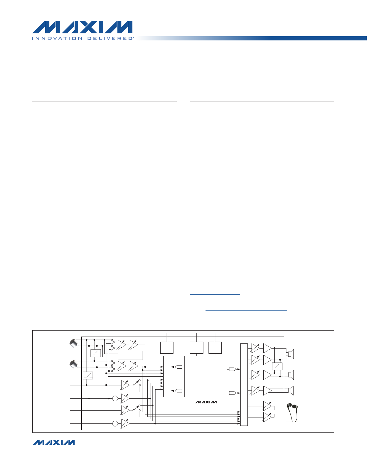
The MAX98088 is a full-featured audio codec whose high
performance and low power consumption make it ideal
for portable applications.
Class D speaker amplifiers provide efficient amplification
for two speakers. Low radiated emissions enable completely filterless operation. Integrated bypass switches
optionally connect an external amplifier to the transducer
when the Class D amplifiers are disabled.
The IC features a stereo Class H headphone amplifier
that utilizes a dual-mode charge pump to maximize efficiency while outputting a ground referenced signal that
does not require output coupling capacitors.
The IC also features a mono differential amplifier that can
also be configured as a stereo line output.
Two differential analog microphone inputs are available as
well as support for two PDM digital microphones. Integrated
switches allow for an additional microphone input as well
as microphone signals to be routed out to external devices.
Two flexible single-ended or differential line inputs may be
connected to an FM radio or other sources.
Integrated FlexSoundK technology improves loudspeaker performance by optimizing the signal level and frequency response while limiting the maximum distortion
and power at the output to prevent speaker damage.
Automatic gain control (AGC) and a noise gate optimize
the signal level of microphone input signals to make best
use of the ADC dynamic range.
The device is fully specified over the -40NC to +85NC
extended temperature range.
FlexSound is a trademark of Maxim Integrated Products, Inc.
Features
S 5.6mW Power Comsumption (DAC to HP at 97dB DR)
S 101dB DR Stereo DAC (8kHz < fS < 96kHz)
S 93dB DR Stereo ADC (8kHz < fS < 96kHz)
S Stereo Low EMI Class D Amplifiers
950mW/Channel (8I, V
SPKVDD�
= 4.2V)
S Efficient Class H Headphone Amplifier
S Differential Receiver Amplifier/Stereo Line Outputs
S 2 Stereo Single-Ended/Mono Differential Line
Inputs
S 3 Differential Microphone Inputs
S FlexSound Technology
5-Band Parametric EQ
Automatic Level Control (ALC)
Excursion Limiter
Speaker Power Limiter
Speaker Distortion Limiter
Microphone Automatic Gain Control
and Noise Gate
S Dual I2S/PCM/TDM Digital Audio Interfaces
S Asynchronous Digital Mixing
S Supports Master Clock Frequencies from 10MHz
to 60MHz
S RF Immune Analog Inputs and Outputs
S Extensive Click-and-Pop Reduction Circuitry
S Available in 63-Bump WLP Package (3.80mm x
3.30mm, 0.4mm Pitch)
Ordering Information appears at end of data sheet.
For related parts and recommended products to use with this part,
refer to www.maxim-ic.com/MAX98088.related.
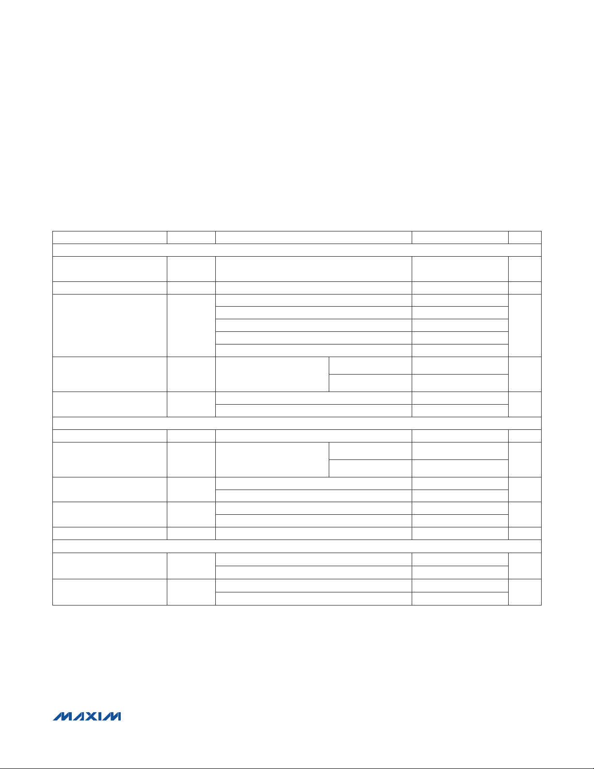
Simplified Block Diagram
2
I2S/PCM
S/PCM
I
AUDIO
TECHNOLOGY
MAX98088
DIGITAL
AUDIO
INTERFACE
DIGITAL
INTERFACE
FlexSound
• 5-BAND PARAMETRIC EQ
• AUTOMATIC LEVEL CONTROL
• LOUDSPEAKER PROCESSING
• EXCURSION LIMITER
• THD LIMITER
• POWER LIMITER
• MICROPHONE PROCESSING
• AUTOMATIC GAIN CONTROL
• NOISE GATE
• ASYNCHRONOUS DIGITAL MIXING
RECEIVER/LINEOUT AMPS
DAC
DAC
SPEAKER AMP
SPEAKER AMP
MIX
HEADPHONE AMP
HEADPHONE AMP
LINEIN A1
LINEIN A2
LINEIN B1
LINEIN B2
DIGITAL MICROPHONE
+
+
I2C
CONTROL
INPUT
ADC
MIX
ADC
����������������������������������������������������������������� Maxim Integrated Products 1
For pricing, delivery, and ordering information, please contact Maxim Direct at 1-888-629-4642,
or visit Maxim’s website at www.maxim-ic.com.

MAX98088
Stereo Audio Codec
with FlexSound Technology
TABLE OF CONTENTS
General Description ............................................................................ 1
Features ..................................................................................... 1
Simplified Block Diagram ........................................................................ 1
Functional Diagram ............................................................................ 5
Absolute Maximum Ratings ...................................................................... 6
Electrical Characteristics ........................................................................6
Digital Input/Output Characteristics ............................................................... 19
Input Clock Characteristics ..................................................................... 21
Audio Interface Timing Characteristics ............................................................22
Digital Microphone Timing Characterstics .......................................................... 23
I2C Timing Characterstics ...................................................................... 24
Power Consumption ........................................................................... 25
Typical Operating Characteristics ................................................................ 28
Microphone to ADC..........................................................................28
Line to ADC................................................................................32
Line-In Pin Direct to ADC .....................................................................33
Digital Loopback ............................................................................33
Analog Loopback ...........................................................................34
DAC to Receiver ............................................................................35
Line to Receiver ............................................................................37
DAC to Line Output..........................................................................38
Line to Line Output ..........................................................................38
DAC to Speaker.............................................................................39
Line to Speaker .............................................................................43
DAC to Headphone..........................................................................44
Line to Headphone ..........................................................................51
Speaker Bypass Switch ......................................................................52
Pin Configuration ............................................................................. 53
Pin Description ............................................................................... 54
Detailed Description........................................................................... 56
I2C Slave Address...........................................................................57
Registers ..................................................................................57
Power Management .........................................................................63
Microphone Inputs ..........................................................................65
Line Inputs.................................................................................67
ADC Input Mixers ...........................................................................68
����������������������������������������������������������������� Maxim Integrated Products 2

MAX98088
Stereo Audio Codec
with FlexSound Technology
TABLE OF CONTENTS (continued)
Record Path Signal Processing.................................................................69
Microphone AGC .........................................................................69
Noise Gate ..............................................................................69
ADC Record Level Control ....................................................................72
Sidetone ..................................................................................73
Digital Audio Interfaces.......................................................................74
Clock Control...............................................................................81
Sample Rate Converter.......................................................................84
Passband Filtering...........................................................................85
Playback Path Signal Processing ...............................................................88
Automatic Level Control ....................................................................88
Parametric Equalizer ......................................................................89
Playback Level Control .......................................................................91
DAC Input Mixers ...........................................................................92
Receiver Amplifier ...........................................................................93
Receiver Output Mixer .....................................................................94
Receiver Output Volume ...................................................................95
Speaker Amplifiers ..........................................................................96
Speaker Output Mixers ....................................................................97
Speaker Amplifier Signal Processing ............................................................98
Excursion Limiter .........................................................................98
Speaker Output Volume ....................................................................98
Power Limiter ...........................................................................101
Distortion Limiter ........................................................................102
Headphone . . . . . . . . . . . . . . . . . . . . . . . . . . . . . . . . . . . . . . . . . . . . . . . . . . . . . . . . . . . . . . . . . . . . . . . . . . . . . . . 103
DirectDrive Headphone Amplifier ...........................................................103
Charge Pump...........................................................................103
Class H Operation .......................................................................104
Headphone Output Mixers.................................................................105
Headphone Output Volume ................................................................10 6
Output Bypass Switches.....................................................................107
Click-and-Pop Reduction ....................................................................108
Jack Detection.............................................................................109
Jack Detection and Removal ...............................................................109
Battery Measurement .......................................................................110
Device Status .............................................................................111
����������������������������������������������������������������� Maxim Integrated Products 3

MAX98088
Stereo Audio Codec
with FlexSound Technology
TABLE OF CONTENTS (CONTINUED)
I2C Serial Interface .........................................................................112
Bit Transfer .............................................................................112
START and STOP Conditions...............................................................112
Early STOP Conditions....................................................................112
Device Revision............................................................................112
Slave Address ..........................................................................113
Acknowledge ...........................................................................113
Write Data Format .......................................................................113
Read Data Format .......................................................................114
Applications Information ........................................................................115
Typical Operating Circuits....................................................................115
Filterless Class D Operation ..................................................................117
RF Susceptibility ...........................................................................117
Startup/Shutdown Sequencing ................................................................117
Component Selection .......................................................................118
Optional Ferrite Bead Filter ................................................................118
Input Capacitor..........................................................................118
Charge-Pump Capacitor Selection ..........................................................118
Charge-Pump Flying Capacitor .............................................................119
Charge-Pump Holding Capacitor ...........................................................119
Unused Pins ..............................................................................119
Recommended PCB Routing .................................................................120
Supply Bypassing, Layout, and Grounding ......................................................120
WLP Applications Information.................................................................121
Ordering Information ......................................................................... 121
Package Information.......................................................................... 122
Revision History ............................................................................. 123
����������������������������������������������������������������� Maxim Integrated Products 4
MAX98088
Stereo Audio Codec
with FlexSound Technology
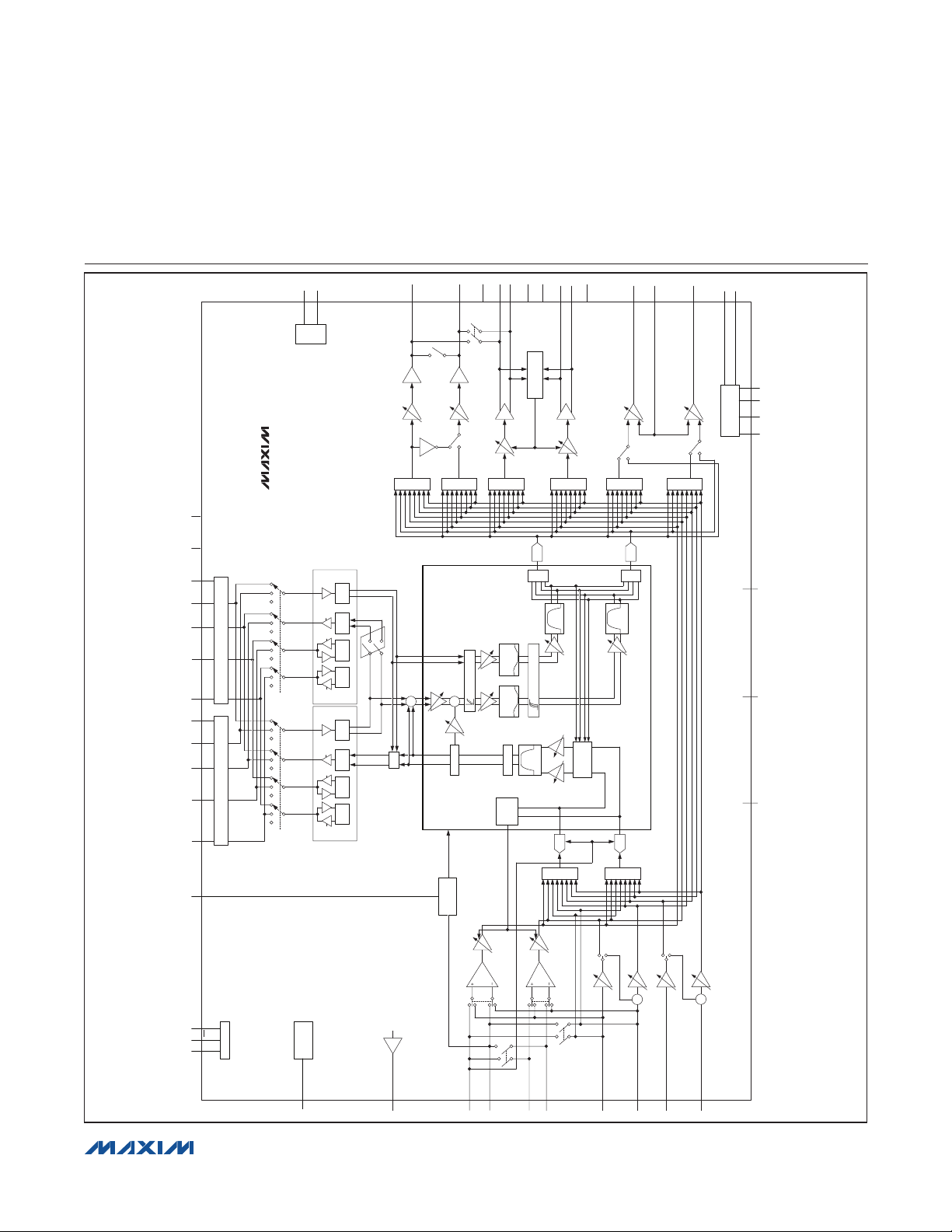
Functional Diagram
F6
REFG6
REG
BIAS
MAX98088
G5
AVDD
G4
DVDD
SDIN2
DATA
INPUT
HIZOFF2SDIEN1 SDIEN2
SDOUT2
DATA
OUTPUT
PORT S2PORT S1
LRCLKS2 SDOUTS2 SDINS2 DVDDS2
LRCLKS1 SDOUTS1 SDINS1 DVDDS1 BCLKS2
D1 D4 D2 E4 E1 F2 F3 G1 G3 G2
BCLKS1
MCLK
MAS2
LRCLK2
FRAME
CLOCK
BIT
BCLK2
SDIN1
SDOUT1
LRCLK1
BCLK1
SEL1 SEL2
CLOCK
MAS2
DAI2
DATA
INPUT
HIZOFF1
DATA
OUTPUT
MAS1
FRAME
CLOCK
BIT
CLOCK
MAS1
DAI1
RECP/
RECVOLL:
LBEN1
MUX
A6
RXINP
LOUTL/
0dB
+8dB TO -62dB
MIX
+
LBEN2
RECN/
LOUTR/
RECBYP
RECLEN
RECVOLR:
+8dB TO -62dB
MIXRECL
TM
DV1G:
0/6/12/18dB
LTEN1
DVST:
0dB TO -60dB
CLOCK
RXINN B6
FlexSound
TECHNOLOGY
+
MIX
SIDETONE
CONTROL
RECREN
0dB
LINEMODE
MIX
MULTI BAND ALC
DSTS
SPKBYP
A3, B3
SPKLVDD
MIXRECR
DVEQ2:
DVEQ1:
A4, B4
SPKLP
SPVOLL:
+8dB TO -62dB
0dB TO -15dB
0dB TO -15dB
A5, B5
SPKLN
+6dB
MIX
5-BAND
PARAMETRIC
5-BAND
PARAMETRIC
NOISE GATE
GAIN
AUTOMATIC
SPLEN
EQ
EQ
CONTROL
C4, C5
SPKLGND
MIXSPL
EQ1ENEQ2EN
AUDIO/
MODE1
C9
C8
SPKRGND A2, B2
+8dB TO -62dB
MIXSPR
CONVERTER
MODE
MIXHPL_
AUDIO/
HPVOLL:
PATH SEL
VOICE
ADCR
HPL
+3dB TO -67dB
MIX
DACR
MIX
FILTERS
MODE1
DV1:
0dB TO -15dB
ADREN
MIX
DAREN
DVFLT
HPLEN
MIXHPL
MIXDAR
MIXADR
HPSNS
HPVOR:
+3dB TO -67dB
MIXHPR_
PATH SEL
MIX
SPKRP C1, C2
SPKRN A1, B1
SPKRVDD C3, D3
POWER/
DISTORTION LIMITER
SPREN
+6dB
SPVOLR:
MIX
DACL
DALEN
MIX
MIXDAL
AUDIO
FILTERS
DCB2
DV2:
0dB TO -15dB
EXCURSION LIMITER
AVRG: 0/6/
12/18dB
AVR:0dB
TO -15dB
VOICE
FILTERS
SAMPLE RATE
AVFLT
SRMIX_
12/18dB
AVL:0dB
TO -15dB
AVLG: 0/6/
ADCL
ADLEN
MIX
MIXADL
A9
HPR D9
PVDD A7
HPGND
B7B8A8
HPREN
HPVSS
PUMP
CHARGE
B9
HPVDD C1N C1P
MIXHPR
F1 G7 C6, C7, D5, D6, D7, E3
DGND AGND N.C.
0/20/30dB
INABYP
PGAINA:
+20dB TO -6dB
INADIFF
INA1/EXTMICP
F9
MIC1N/
DIGMICCLK
F8
PA1EN:
EXTMIC
0/20/30dB
MIC2BYP
PGAM2:
+20dB TO 0dB
G9 MIC2P
PA2EN:
EXTMIC
G8 MIC2N
PGAM1:
+20dB TO 0dB
E5F5F4 E2
IRQ
C
2
I
SCL
SDA
JACK
JACKSNS
E6
DETECTION
JDETEN
REG
MBEN
MIC1P/
MICBIAS
F7
DIGMICDATA
E8
PGAINA:
+20dB TO -6dB
INA2/EXTMICN
E9
INBDIFF
PGAINB:
+20dB TO -6dB
PGAINB:
+20dB TO -6dB
+
+
INB2
INB1
E7
D8
����������������������������������������������������������������� Maxim Integrated Products 5
MAX98088
Stereo Audio Codec
with FlexSound Technology
ABSOLUTE MAXIMUM RATINGS
(Voltages with respect to AGND.)
DVDD, AVDD, PVDD, HPVDD .............................. -0.3V to +2.2V
SPKLVDD, SPKRVDD, DVDDS1, DVDDS2 .......... -0.3V to +6.0V
DGND, HPGND, SPKLGND, SPKRGND .............. -0.1V to +0.1V
HPVSS ............................... (HPGND - 2.2V) to (HPGND + 0.3V)
C1N .................................... (HPVSS - 0.3V) to (HPGND + 0.3V)
C1P .....................................(HPGND - 0.3V) to (HPVDD + 0.3V)
REF, MICBIAS ................................. -0.3V to (SPKLVDD + 0.3V)
MCLK, SDINS1, SDINS2, JACKSNS,
SDA, SCL, IRQ .................................................-0.3V to +6.0V
LRCLKS1, BCLKS1, SDOUTS1 ......... -0.3V to (DVDDS1 + 0.3V)
LRCLKS2, BCLKS2, SDOUTS2 ......... -0.3V to (DVDDS2 + 0.3V)
Stresses beyond those listed under “Absolute Maximum Ratings” may cause permanent damage to the device. These are stress ratings only, and functional operation of the device at these or any other conditions beyond those indicated in the operational sections of the specifications is not implied. Exposure to absolute
maximum rating conditions for extended periods may affect device reliability.
ELECTRICAL CHARACTERISTICS
(V
= V
AVDD
SPK_P and SPK_N. Receiver load (R
to HPGND. Line out loads (R
= 2.2FF, C
= 0dB, AV
MCLK = 12.288MHz, LRCLK = 48kHz, MAS = 1. TA = T
PARAMETER SYMBOL CONDITIONS MIN TYP MAX UNITS
POWER SUPPLY
Supply Voltage Range Guaranteed by PSRR
Total Supply Current
(Notes 2 and 3)
Shutdown Supply Current
(Note 2)
REF Voltage 2.5 V
REG Voltage 0.79 V
Shutdown to Full Operation
= V
PVDD
MICBIAS
DACGAIN
= V
DVDD
= C
REG
= 0dB, AV
= V
DVDDS1
) connected between RECP and RECN. Headphone loads (RHP) connected from HPL or HPR
REC
) connected from LOUTL or LOUTR to SPKLGND. R
LOAD
= 1FF, C
C1N-C1P
ADCLVL
= 0dB, AV
DVDDS2
= 1FF, C
= +1.8V, V
HPVDD
ADCGAIN
MIN
SPKLVDD
= C
= 0dB, AV
to T
Full-duplex 8kHz mono,
receiver output, MAS = 1
DAC playback 48kHz
I
VDD
stereo, headphone
outputs, MAS = 1
DAC playback 48kHz
stereo, speaker outputs,
MAS = 1
TA = +25NC
VSEN = 0
VSEN = 1
REG, INA1/EXTMICP, INA2/EXTMICN, INB1,
INB2, MIC1P/DIGMICDATA, MIC1N/DIGMICCLK,
MIC2P, MIC2N .................................................. -0.3V to +2.2V
HPSNS ............................... (HPGND - 0.3V) to (HPGND + 0.3V)
HPL, HPR ............................ (HPVSS - 0.3V) to (HPVDD + 0.3V)
RECP/LOUTL/RXINP, RECN/LOUTR/
RXINN .....................(SPKLGND - 0.3V) to (SPKLVDD + 0.3V)
SPKLP, SPKLN ...........(SPKLGND - 0.3V) to (SPKLVDD + 0.3V)
SPKRP, SPKRN .........(SPKRGND - 0.3V) to (SPKRVDD + 0.3V)
Continuous Power Dissipation (TA = +70NC)
63-Bump WLP (derate 25.6mW/NC above +70NC) ........2.05W
Operating Temperature Range .......................... -40NC to +85NC
Storage Temperature Range ............................ -65NC to +150NC
Soldering Temperature (reflow) ......................................+260NC
= V
SPKRVDD
= 1FF. AV
HPVSS
PGAIN_
, unless otherwise noted. Typical values are at +25NC.) (Note 1)
MAX
V
SPKLVDD
DVDD
V
DVDDS1
= 3.7V. Speaker loads (Z
= RHP = J, R
LOAD
SPKRVDD
, V
PVDD
DVDDS2
= +20dB, AV
= 0dB, AV
HP_
MICPRE_
= 0dB, AV
, V
, V
AVDD
, V
) connected between
SPK
= J, Z
REC
MICPGA_
= 0dB, AV
REC
SPK
= 0dB, AV
2.8 5.5
1.65 1.8 2
1.65 3.6
= J, C
SPK_
Analog 4.5 8
Speaker 1.6 2.3
Digital 1.3 2
Analog 1.9 3
Speaker 0.001 0.0058
Digital 2.47 3.5
Analog 3.6 6.5
Speaker 6.41 8.5
Digital 2.49 3.5
Analog 0.2 2
Speaker 0.01 1
Digital 1 5
30
17
REF
DACATTN
= 0dB,
VV
mA
FA
ms
����������������������������������������������������������������� Maxim Integrated Products 6
with FlexSound Technology
ELECTRICAL CHARACTERISTICS (continued)
(V
= V
AVDD
SPK_P and SPK_N. Receiver load (R
to HPGND. Line out loads (R
= 2.2FF, C
= 0dB, AV
MCLK = 12.288MHz, LRCLK = 48kHz, MAS = 1. TA = T
PARAMETER SYMBOL CONDITIONS MIN TYP MAX UNITS
MICROPHONE TO ADC PATH
Dynamic Range DR
Total Harmonic Distortion +
Noise
Common-Mode Rejection
Ratio
Power-Supply Rejection Ratio PSRR
Path Phase Delay
MICROPHONE PREAMP
Full-Scale Input AV
Preamplifier Gain AV
PGA Gain AV
MIC Input Resistance R
= V
PVDD
MICBIAS
DACGAIN
= V
DVDD
= C
REG
= 0dB, AV
= V
DVDDS1
) connected between RECP and RECN. Headphone loads (RHP) connected from HPL or HPR
REC
) connected from LOUTL or LOUTR to SPKLGND. R
LOAD
= 1FF, C
C1N-C1P
ADCLVL
= 0dB, AV
DVDDS2
= 1FF, C
= +1.8V, V
HPVDD
ADCGAIN
MIN
SPKLVDD
= C
HPVSS
= 0dB, AV
to T
MAX
fS = 8kHz, MODE = 0 (IIR voice), AV
(Note 4)
VIN = 0.1V
THD+N
MICPRE_
AV
MICPRE_
CMRR VIN = 100mV
V
AVDD
, fS = 8kHz, f = 1kHz -78
P-P
= 0dB, VIN = 1V
= +30dB, VIN = 32mV
, f = 217Hz 74 dB
P-P
= 1.65V to 1.95V, input referred,
MIC inputs floating
= 200mV
RIPPLE
f = 1kHz, V
f = 10kHz, V
RIPPLE
RIPPLE
= 200mV
= 200mV
1kHz, 0dB input,
highpass filter disabled
measured from analog
input to digital output
= 0dB 1.05 V
MICPRE_
MICPGA_
IN_MIC
MICPRE_
(Note 5)
(Note 5)
All gain settings, measured at MIC1P/
MIC1N/MIC2P/MIC2N
MAX98088
Stereo Audio Codec
= V
SPKRVDD
= 1FF. AV
PGAIN_
, unless otherwise noted. Typical values are at +25NC.) (Note 1)
P-P
P-P
P-P
P-P
MODE = 0 (IIR voice)
8kHz
MODE = 0 (IIR voice)
16kHz
MODE = 1 (FIR audio)
8kHz
MODE = 1 (FIR audio)
48kHz
PA1EN/PA2EN = 01 0
PA1EN/PA2EN = 11 29.5 30 30.5
PGAM1/PGAM2 = 0x00 19 20 21
PGAM1/PGAM2 = 0x14 0
= 3.7V. Speaker loads (Z
= RHP = J, R
LOAD
MICPRE_
= 0dB, AV
MICPRE_
= +20dB, AV
= 0dB, AV
HP_
= 0dB
SPK
REC
MICPGA_
= 0dB, AV
REC
88 dB
, f = 1kHz -85
, f = 1kHz -71
P-P
50 62
, input referred 62
, input referred 62
, input referred 53
2.2
1.1
4.5
0.76
50
) connected between
= J, Z
= 0dB, AV
SPK
= J, C
DACATTN
SPK_
REF
= 0dB,
dBAV
dBf = 217Hz, V
ms
P-P
dBPA1EN/PA2EN = 10 19.5 20 20.5
dB
kI
����������������������������������������������������������������� Maxim Integrated Products 7
MAX98088
Stereo Audio Codec
with FlexSound Technology
ELECTRICAL CHARACTERISTICS (continued)
(V
= V
AVDD
SPK_P and SPK_N. Receiver load (R
to HPGND. Line out loads (R
= 2.2FF, C
= 0dB, AV
MCLK = 12.288MHz, LRCLK = 48kHz, MAS = 1. TA = T
PARAMETER SYMBOL CONDITIONS MIN TYP MAX UNITS
MICROPHONE BIAS
MICBIAS Output Voltage V
Load Regulation I
Line Regulation V
Ripple Rejection
Noise Voltage
MICROPHONE BYPASS SWITCH
On-Resistance R
Total Harmonic Distortion +
Noise
Off-Isolation
Off-Leakage Current
LINE INPUT TO ADC PATH
Dynamic Range (Note 4) DR
Total Harmonic Distortion +
Noise
Gain Error DC accuracy 1 %
Power-Supply Rejection Ratio PSRR
= V
PVDD
MICBIAS
DACGAIN
= V
DVDD
= C
REG
= 0dB, AV
= V
DVDDS1
) connected between RECP and RECN. Headphone loads (RHP) connected from HPL or HPR
REC
) connected from LOUTL or LOUTR to SPKLGND. R
LOAD
= 1FF, C
C1N-C1P
= 0dB, AV
ADCLVL
MICBIASILOAD
DVDDS2
= 1FF, C
LOAD
SPKLVDD
f = 217Hz, V
f = 10kHz, V
= +1.8V, V
HPVDD
ADCGAIN
MIN
SPKLVDD
= C
= 0dB, AV
to T
= V
HPVSS
, unless otherwise noted. Typical values are at +25NC.) (Note 1)
MAX
= 1mA 2.15 2.2 2.25 V
= 1mA to 2mA 0.5 4.5 mV
= 2.8V to 5.5V 110
RIPPLE (SPKLVDD)
RIPPLE (SPKLVDD)
A-weighted, f = 20Hz to 20kHz 3.9
P-weighted, f = 20Hz to 4kHz 2.1
f = 1kHz 50
I
= 100mA, INABYP = MIC2BYP = 1,
ON
THD+N
MIC1_
V
MIC2_
VIN = 2V
= V
= 0V, AVDD, TA = +25NC
INA_
, VCM = 0.9V, RL = 10kI,
P-P
f = 1kHz, INABYP = MIC2BYP = 1
VIN = 2V
V
MIC1_
, VCM = 0.9V, RL = 10kI, f = 1kHz
P-P
= [0V, AVDD], V
MIC2_/VINA_
[AVDD, 0V]
INA pin direct, fS = 48kHz, MODE = 1
(FIR audio)
THD+N VIN = 1V
V
AVDD
, f = 1kHz -82 -74 dB
P-P
= 1.65V to 1.95V, input referred,
line inputs floating, TA = +25NC
f = 217Hz, V
AV
= 0dB, input referred
ADC
f = 1kHz, V
AV
= 0dB, input referred
ADC
f = 10kHz, V
AV
= 0dB, input referred
ADC
RIPPLE
RIPPLE
RIPPLE
= 200mV
= 200mV
= 200mV
SPKRVDD
= 1FF. AV
= 0dB, AV
PGAIN_
= 100mV
= 100mV
,
P-P
,
P-P
,
P-P
= 3.7V. Speaker loads (Z
= RHP = J, R
LOAD
HP_
P-P
P-P
= +20dB, AV
= 0dB, AV
-1 +1
MICPRE_
=
57 68
) connected between
SPK
= J, Z
REC
MICPGA_
REC
= 0dB, AV
= 0dB, AV
92
83
5 30
-80 dB
60 dB
93 dB
63
63
57
SPK
= J, C
DACATTN
SPK_
= 0dB,
FV
nV/√Hz
FV
dB
RMS
I
FA
dB
REF
����������������������������������������������������������������� Maxim Integrated Products 8
MAX98088
Stereo Audio Codec
with FlexSound Technology
ELECTRICAL CHARACTERISTICS (continued)
(V
= V
AVDD
SPK_P and SPK_N. Receiver load (R
to HPGND. Line out loads (R
= 2.2FF, C
= 0dB, AV
MCLK = 12.288MHz, LRCLK = 48kHz, MAS = 1. TA = T
PARAMETER SYMBOL CONDITIONS MIN TYP MAX UNITS
LINE INPUT PREAMP
Full-Scale Input V
Level Adjust Gain AV
Input Resistance R
Feedback Resistance R
ADC LEVEL CONTROL
ADC Level Adjust Range AV
ADC Level Step Size 1 dB
ADC Gain Adjust Range AV
ADC Gain Adjust Step Size 6 dB
ADC DIGITAL FILTERS
VOICE MODE IIR LOWPASS FILTER (MODE1 = 0)
Passband Cutoff f
Passband Ripple f < f
Stopband Cutoff f
Stopband Attenuation
(Note 6)
= V
PVDD
MICBIAS
DACGAIN
= V
DVDD
= C
REG
= 0dB, AV
= V
DVDDS1
) connected between RECP and RECN. Headphone loads (RHP) connected from HPL or HPR
REC
) connected from LOUTL or LOUTR to SPKLGND. R
LOAD
= 1FF, C
C1N-C1P
ADCLVL
PGAIN_
IN_FB
ADCLVL
ADCGAIN
PLP
SLP
= 0dB, AV
IN
IN
DVDDS2
= 1FF, C
AV
AV
= +1.8V, V
ADCGAIN
PGAIN_
PGAIN_
SPKLVDD
= C
HPVDD
= 0dB, AV
to T
MIN
= 0dB 1
= -6dB 1.4
= V
HPVSS
, unless otherwise noted. Typical values are at +25NC.) (Note 1)
MAX
TA = +25NC
(Note 5)
AV
AV
AV
AV
AV
AV
= +20dB 14.5 21 28
PGAIN_
= +14dB 20
PGAIN_
= +3dB 20
PGAIN_
= 0dB 7.5 10 14
PGAIN_
= -3dB 20
PGAIN_
= -6dB 20
PGAIN_
INAEXT/INBEXT = 1
AVL/AVR = 0xF to 0x0 (Note 5) -12 +3 dB
AVLG/AVRG = 00 to 11 (Note 5) 0 18 dB
Ripple limit cutoff 0.441 x fs
-3dB cutoff 0.449 x fs
PLP
0.47 x f
f > f
SLP
SPKRVDD
= 1FF. AV
= 0dB, AV
PGAIN_
= 3.7V. Speaker loads (Z
= RHP = J, R
LOAD
MICPRE_
= +20dB, AV
= 0dB, AV
HP_
) connected between
SPK
= J, Z
REC
MICPGA_
REC
= 0dB, AV
= 0dB, AV
SPK
PGAINA/PGAINB = 0x0 19 20 21
PGAINA/PGAINB = 0x1 13 14 15
PGAINA/PGAINB = 0x2 2 3 4
PGAINA/PGAINB = 0x3 0
PGAINA/PGAINB = 0x4 -4 -3 -2
PGAINA/PGAINB = 0x5,
0x6, 0x7
TA = +25NC
TA = T
MIN
to T
MAX
-7 -6 -5
18 20 22
16 24
-0.1 +0.1 dB
74 dB
= J, C
DACATTN
SPK_
S
= 0dB,
V
P-P
dB
kI
kI
Hz
Hz
REF
����������������������������������������������������������������� Maxim Integrated Products 9
Stereo Audio Codec
with FlexSound Technology
ELECTRICAL CHARACTERISTICS (continued)
(V
= V
AVDD
SPK_P and SPK_N. Receiver load (R
to HPGND. Line out loads (R
= 2.2FF, C
= 0dB, AV
MCLK = 12.288MHz, LRCLK = 48kHz, MAS = 1. TA = T
PARAMETER SYMBOL CONDITIONS MIN TYP MAX UNITS
VOICE MODE IIR HIGHPASS FILTER (MODE1 = 0)
Passband Cutoff
(-3dB from Peak)
Stopband Cutoff
(-30dB from Peak)
DC Attenuation DC
STEREO AUDIO MODE FIR LOWPASS FILTER (MODE1 = 1, DHF1 = 0, LRCLK < 50kHz)
Passband Cutoff f
Passband Ripple f < f
Stopband Cutoff f
Stopband Attenuation
(Note 6)
ADC STEREO AUDIO MODE FIR LOWPASS FILTER (MODE1 = 1, DHF1 = 1, LRCLK > 50kHz)
Passband Cutoff f
Passband Ripple f < f
Stopband Cutoff f
Stopband Attenuation f < f
= V
PVDD
MICBIAS
DACGAIN
= V
DVDD
= C
REG
= 0dB, AV
= V
DVDDS1
) connected between RECP and RECN. Headphone loads (RHP) connected from HPL or HPR
REC
) connected from LOUTL or LOUTR to SPKLGND. R
LOAD
= 1FF, C
C1N-C1P
ADCLVL
= 0dB, AV
DVDDS2
= 1FF, C
= +1.8V, V
HPVDD
ADCGAIN
MIN
SPKLVDD
= C
HPVSS
= 0dB, AV
to T
, unless otherwise noted. Typical values are at +25NC.) (Note 1)
MAX
= V
AVFLT = 0x1 (Elliptical tuned for fS = 16kHz +
217Hz notch)
AVFLT = 0x2 (500Hz Butterworth tuned for fS =
16kHz)
f
AHPPB
AVFLT = 0x3 (Elliptical tuned for fS = 8kHz +
217Hz notch)
AVFLT = 0x4 (500Hz Butterworth tuned for fS =
8kHz)
AVFLT = 0x5 (fS/240 Butterworth)
AVFLT = 0x1 (Elliptical tuned for fS = 16kHz +
217Hz notch)
AVFLT = 0x2 (500Hz Butterworth tuned for fS =
16kHz)
f
AHPSB
AVFLT = 0x3 (Elliptical tuned for fS = 8kHz +
217Hz notch)
AVFLT = 0x4 (500Hz Butterworth tuned for fS =
8kHz)
AVFLT = 0x5 (fS/240 Butterworth)
ATTEN
AVFLT ≠ 000
Ripple limit cutoff 0.43 x f
PLP
-6.02dB cutoff 0.5 x f
PLP
SLP
f < f
SLP
PLP
SLP
Ripple limit cutoff 0.208 x f
-3dB cutoff 0.28 x f
PLP
SLP
SPKRVDD
= 1FF. AV
= 0dB, AV
PGAIN_
= 3.7V. Speaker loads (Z
= RHP = J, R
LOAD
MICPRE_
= +20dB, AV
= 0dB, AV
HP_
MAX98088
) connected between
SPK
= J, Z
REC
MICPGA_
REC
= 0dB, AV
= 0dB, AV
0.0139
x f
S
0.0156
x f
S
0.0279
x f
S
0.0312
x f
S
0.0018
x f
S
90 dB
S
S
S
-0.1 +0.1 dB
60 dB
S
S
-0.1 +0.1 dB
0.417 x fSHz
60 dB
= J, C
SPK
DACATTN
SPK_
0.0161
x f
S
0.0319
x f
S
0.0321
x f
S
0.0632
x f
S
0.0043
x f
S
0.58 x fSHz
REF
= 0dB,
Hz
Hz
Hz-3dB cutoff 0.48 x f
Hz
���������������������������������������������������������������� Maxim Integrated Products 10
MAX98088
Stereo Audio Codec
with FlexSound Technology
ELECTRICAL CHARACTERISTICS (continued)
(V
= V
AVDD
SPK_P and SPK_N. Receiver load (R
to HPGND. Line out loads (R
= 2.2FF, C
= 0dB, AV
MCLK = 12.288MHz, LRCLK = 48kHz, MAS = 1. TA = T
PARAMETER SYMBOL CONDITIONS MIN TYP MAX UNITS
ADC STEREO AUDIO MODE DC BLOCKING HIGHPASS FILTER (MODE1 = 1)
Passband Cutoff
(-3dB from Peak)
DC Attenuation DC
MICROPHONE AUTOMATIC GAIN CONTROL
AGC Hold Duration
AGC Attack Time
AGC Release Time
AGC Threshold Level AGCTH = 0x0 to 0xF -3 +18 dB
AGC Threshold Step Size 1 dB
AGC Gain (Note 5) 0 20 dB
ADC NOISE GATE
NG Threshold Level ANTH = 0x3 to 0xF, referred to 0dBFS -64 -16 dB
NG Attenuation (Note 5) 0 12 dB
ADC-TO-DAC DIGITAL SIDETONE (MODE = 0)
Sidetone Gain Adjust Range AV
Sidetone Gain Adjust Step
Size
Sidetone Path Phase Delay
ADC-TO-DAC DIGITAL LOOP-THROUGH PATH
Dynamic Range (Note 4) DR
Total Harmonic Distortion +
Noise
DAC LEVEL CONTROL
DAC Attenuation Range AV
DAC Attenuation Step Size 1 dB
DAC Gain Adjust Range AV
DAC Gain Adjust Step Size 6 dB
= V
PVDD
MICBIAS
DACGAIN
= V
DVDD
= C
REG
= 0dB, AV
= V
DVDDS1
) connected between RECP and RECN. Headphone loads (RHP) connected from HPL or HPR
REC
) connected from LOUTL or LOUTR to SPKLGND. R
LOAD
= 1FF, C
C1N-C1P
ADCLVL
f
AHPPB
= 0dB, AV
Atten
= +1.8V, V
DVDDS2
= 1FF, C
AVFLT ≠ 000
AVFLT ≠ 000
HPVDD
ADCGAIN
MIN
SPKLVDD
= C
HPVSS
= 0dB, AV
to T
, unless otherwise noted. Typical values are at +25NC.) (Note 1)
MAX
= V
AGCHLD = 01 50
AGCHLD = 11 400
AGCATK = 00 2
AGCATK = 11 123
AGCRLS = 000 0.078
AGCRLS = 111 10
STGA
DVST = 0x01 -0.5
DVST = 0x1F -60.5
1kHz, 0dB input, highpass filter
disabled
fS = 48kHz, MCLK = 12.288MHz, MODE = 1
(FIR audio), MIC to HP output, TA = +25NC
THD+N
DACATTN
DACGAIN
f = 1kHz, fS = 48kHz, MCLK = 12.288MHz, MODE
= 1 (FIR audio), MIC to HP output
DV_ = 0xF to 0x0 (Note 5) -15 0 dB
DV1G = 00 to 11 (Note 5) 0 18 dB
SPKRVDD
= 1FF. AV
= 0dB, AV
PGAIN_
= 3.7V. Speaker loads (Z
= RHP = J, R
LOAD
MICPRE_
= +20dB, AV
= 0dB, AV
HP_
SPK
REC
MICPGA_
= 0dB, AV
REC
90 dB
8kHz 2.2
16kHz 1.1
83 93 dB
81 dB
) connected between
= J, Z
= 0dB, AV
SPK
= J, C
DACATTN
SPK_
= 0dB,
0.000125
x f
S
2 dB
Hz
ms
ms
s
dB
ms
REF
���������������������������������������������������������������� Maxim Integrated Products 11
Stereo Audio Codec
with FlexSound Technology
ELECTRICAL CHARACTERISTICS (continued)
(V
= V
AVDD
SPK_P and SPK_N. Receiver load (R
to HPGND. Line out loads (R
= 2.2FF, C
= 0dB, AV
MCLK = 12.288MHz, LRCLK = 48kHz, MAS = 1. TA = T
PARAMETER SYMBOL CONDITIONS MIN TYP MAX UNITS
DAC DIGITAL FILTERS
VOICE MODE IIR LOWPASS FILTER (MODE1 = 0)
Passband Cutoff f
Passband Ripple f < f
Stopband Cutoff f
Stopband Attenuation (Note 6) f > f
VOICE MODE IIR HIGHPASS FILTER (MODE1 = 0)
Passband Cutoff
(-3dB from Peak)
Stopband Cutoff
(-30dB from Peak)
DC Attenuation DC
STEREO AUDIO MODE FIR LOWPASS FILTER (MODE1 = 1, DHF1/DHF2 = 0, LRCLK < 50kHz)
Passband Cutoff f
Passband Ripple f < f
Stopband Cutoff f
Stopband Attenuation (Note 6) f > f
= V
PVDD
MICBIAS
DACGAIN
= V
DVDD
= C
REG
= 0dB, AV
= V
DVDDS1
) connected between RECP and RECN. Headphone loads (RHP) connected from HPL or HPR
REC
) connected from LOUTL or LOUTR to SPKLGND. R
LOAD
= 1FF, C
C1N-C1P
ADCLVL
PLP
SLP
= 0dB, AV
DVDDS2
= 1FF, C
= +1.8V, V
HPVDD
ADCGAIN
MIN
SPKLVDD
= C
= 0dB, AV
to T
= V
HPVSS
, unless otherwise noted. Typical values are at +25NC.) (Note 1)
MAX
Ripple limit cutoff 0.448 x f
-3dB cutoff 0.451 x f
PLP
SLP
DVFLT = 0x1 (Elliptical tuned for fS = 16kHz +
217Hz notch)
DVFLT = 0x2 (500Hz Butterworth tuned for fS =
16kHz)
f
DHPPB
DVFLT = 0x3 (Elliptical tuned for fS = 8kHz +
217Hz notch)
DVFLT = 0x4 (500Hz Butterworth tuned for fS =
8kHz)
DVFLT = 0x5 (fs/240 Butterworth)
DVFLT = 0x1 (Elliptical tuned for fS = 16kHz +
217Hz notch)
DVFLT = 0x2 (500Hz Butterworth tuned for fS =
16kHz)
f
DHPSB
DVFLT = 0x3 (Elliptical tuned for fS = 8kHz +
217Hz notch)
DVFLT = 0x4 (500Hz Butterworth tuned for fS =
8kHz)
DVFLT = 0x5 (fS/240 Butterworth) 0.0021 x f
ATTEN
DVFLT ≠ 000
Ripple limit cutoff 0.43 x f
PLP
-3dB cutoff 0.47 x f
-6.02dB cutoff 0.5 x f
PLP
SLP
SLP
SPKRVDD
= 1FF. AV
= 0dB, AV
PGAIN_
= 3.7V. Speaker loads (Z
= RHP = J, R
LOAD
MICPRE_
= +20dB, AV
= 0dB, AV
HP_
MAX98088
) connected between
SPK
= J, Z
REC
MICPGA_
REC
= 0dB, AV
= 0dB, AV
S
S
-0.1 +0.1 dB
0.476 x f
75 dB
0.0139 x f
0.0156 x f
0.0279 x f
0.0312 x f
S
S
S
S
S
85 dB
S
S
S
-0.1 +0.1 dB
60 dB
= J, C
SPK
DACATTN
SPK_
S
0.0161
x f
S
0.0312
x f
S
0.0321
x f
S
0.0625
x f
S
0.0042
x f
S
0.58 x fSHz
REF
= 0dB,
Hz
Hz
Hz
Hz
Hz
���������������������������������������������������������������� Maxim Integrated Products 12
MAX98088
Stereo Audio Codec
with FlexSound Technology
ELECTRICAL CHARACTERISTICS (continued)
(V
= V
AVDD
SPK_P and SPK_N. Receiver load (R
to HPGND. Line out loads (R
= 2.2FF, C
= 0dB, AV
MCLK = 12.288MHz, LRCLK = 48kHz, MAS = 1. TA = T
PARAMETER SYMBOL CONDITIONS MIN TYP MAX UNITS
STEREO AUDIO MODE FIR LOWPASS FILTER (MODE1 = 1, DHF1/DHF2 = 1 for LRCLK > 50kHz)
Passband Cutoff f
Passband Ripple f < f
Stopband Cutoff f
Stopband Attenuation
(Note 6)
STEREO AUDIO MODE DC BLOCKING HIGHPASS FILTER
Passband Cutoff
(-3dB from Peak)
DC Attenuation DC
AUTOMATIC LEVEL CONTROL
Dual Band Lowpass Corner
Frequency
Dual Band Highpass Corner
Frequency
Gain Range 0 12 dB
Low-Signal Threshold ALCTH = 111 to 001 -48 -12 dBFS
Release Time
PARAMETRIC EQUALIZER
Number of Bands 5 Bands
Per Band Gain Range -12 +12 dB
Preattenuator Gain Range (Note 5) -15 0 dB
Preattenuator Step Size 1 dB
DAC TO RECEIVER AMPLIFIER PATH
Dynamic Range DR fS = 48kHz, f = 1kHz (Note 4) 96 dB
Total Harmonic Distortion +
Noise
Power-Supply Rejection Ratio PSRR
Click-and-Pop Level K
= V
PVDD
MICBIAS
DACGAIN
= V
DVDD
= C
REG
= 0dB, AV
= V
DVDDS1
) connected between RECP and RECN. Headphone loads (RHP) connected from HPL or HPR
REC
) connected from LOUTL or LOUTR to SPKLGND. R
LOAD
= 1FF, C
C1N-C1P
ADCLVL
PLP
SLP
f
DHPPB
ATTEN
= 0dB, AV
DVDDS2
= 1FF, C
= +1.8V, V
HPVDD
ADCGAIN
MIN
SPKLVDD
= C
= 0dB, AV
to T
= V
HPVSS
, unless otherwise noted. Typical values are at +25NC.) (Note 1)
MAX
Ripple limit cutoff 0.24 x f
-3dB cutoff 0.31 x f
PLP
f < f
SLP
DVFLT ≠ 000 (DAI1), DCB2 = 1 (DAI2)
DVFLT ≠ 000 (DAI1), DCB2 = 1 (DAI2)
ALCMB = 1 5 kHz
ALCMB = 1 5 kHz
ALCRLS = 101 0.25
ALCRLS = 000 8
THD+N
f = 1kHz, P
V
SPKLVDD
= 2.8V to 5.5V, TA = +25NC
f = 217Hz, V
f = 1kHz, V
f = 10kHz, V
= 15mW, R
OUT
RIPPLE
RIPPLE
RIPPLE
= 200mV
= 200mV
= 200mV
Peak voltage, A-weighted, 32
samples per second, AV
CP
REC
0dB
SPKRVDD
= 1FF. AV
PGAIN_
REC
P-P
P-P
P-P
= 3.7V. Speaker loads (Z
= RHP = J, R
LOAD
MICPRE_
= 0dB, AV
= +20dB, AV
HP_
= 32I
= 0dB, AV
Into shutdown -68
=
Out of shutdown -72
) connected between
SPK
REC
MICPGA_
= 0dB, AV
REC
S
S
= J, Z
= 0dB, AV
SPK
= J, C
DACATTN
SPK_
= 0dB,
Hz
-0.1 +0.1 dB
0.477 x fSHz
60 dB
0.000104
x f
S
Hz
90 dB
-70 -63 dB
64 75
-59
-59
dB
-59
dBV
s
REF
���������������������������������������������������������������� Maxim Integrated Products 13
MAX98088
Stereo Audio Codec
with FlexSound Technology
ELECTRICAL CHARACTERISTICS (continued)
(V
= V
AVDD
SPK_P and SPK_N. Receiver load (R
to HPGND. Line out loads (R
= 2.2FF, C
= 0dB, AV
MCLK = 12.288MHz, LRCLK = 48kHz, MAS = 1. TA = T
PARAMETER SYMBOL CONDITIONS MIN TYP MAX UNITS
LINE INPUT TO RECEIVER AMPLIFIER PATH
Dynamic Range (Note 4) DR Referenced to full-scale output level 94 dB
Total Harmonic Distortion +
Noise
Click-and-Pop Level K
RECEIVER AMPLIFIER
Output Power P
Full-Scale Output (Note 7) 1 V
Volume Control (Note 5) AV
Volume Control Step Size
Mute Attenuation f = 1kHz 88 dB
Capacitive Drive Capability No sustained oscillations
DAC TO LINE OUT AMPLIFIER PATH
Dynamic Range (Note 4) DR fS = 48kHz, f = 1kHz 83 96 dB
Total Harmonic Distortion +
Noise
LINE INPUT TO LINE OUT AMPLIFIER PATH
Dynamic Range (Note 4) DR Referenced to full-scale output level 92 dB
Total Harmonic Distortion +
Noise
Full-Scale Output (Note 7) 2 V
Mute Attenuation f = 1kHz 85 dB
Output Offset Voltage V
Capacitive Drive Capability
= V
PVDD
MICBIAS
DACGAIN
= V
DVDD
= C
REG
= 0dB, AV
= V
DVDDS1
) connected between RECP and RECN. Headphone loads (RHP) connected from HPL or HPR
REC
) connected from LOUTL or LOUTR to SPKLGND. R
LOAD
= 1FF, C
C1N-C1P
ADCLVL
= 0dB, AV
DVDDS2
= 1FF, C
= +1.8V, V
HPVDD
ADCGAIN
MIN
SPKLVDD
= C
HPVSS
= 0dB, AV
to T
, unless otherwise noted. Typical values are at +25NC.) (Note 1)
MAX
= V
SPKRVDD
= 1FF. AV
PGAIN_
= 3.7V. Speaker loads (Z
= RHP = J, R
LOAD
MICPRE_
= 0dB, AV
= +20dB, AV
= 0dB, AV
HP_
) connected between
SPK
= J, Z
REC
MICPGA_
REC
= 0dB, AV
= 0dB, AV
THD+N -64 dB
CP
OUT
REC
Peak voltage, A-weighted, 32
samples per second, AV
REC
0dB
R
= 32I, f = 1kHz, THD = 1%
REC
RECVOL = 0x00 -62
RECVOL = 0x1F 8
Into shutdown -51
=
Out of shutdown -49
83 mW
+8dB to +6dB 0.5
+6dB to +0dB 1
0dB to -14dB 2
-14dB to -38dB 3
-38dB to -62dB 4
500
100
-78 -72 dB
76 dB
Q3.0 Q4
500 pF
THD+N
THD+N
OS
R
REC
R
REC
f = 1kHz, RL = 1kI
f = 1kHz, RL = 10kI
AV
= -62dB
REC_
No sustained oscillations, RL = 1kI
= 32I
= J
SPK
= J, C
DACATTN
SPK_
= 0dB,
dBV
RMS
dB
dB
pF
P-P
mV
REF
���������������������������������������������������������������� Maxim Integrated Products 14
MAX98088
Stereo Audio Codec
with FlexSound Technology
ELECTRICAL CHARACTERISTICS (continued)
(V
= V
AVDD
SPK_P and SPK_N. Receiver load (R
to HPGND. Line out loads (R
= 2.2FF, C
= 0dB, AV
MCLK = 12.288MHz, LRCLK = 48kHz, MAS = 1. TA = T
PARAMETER SYMBOL CONDITIONS MIN TYP MAX UNITS
DAC TO SPEAKER AMPLIFIER PATH
Total Harmonic Distortion +
Noise
Crosstalk
Output Noise 53
Click-and-Pop Level K
MIC INPUT TO SPEAKER AMPLIFIER PATH
Dynamic Range (Note 4) DR Referenced to full-scale output level, AV
Total Harmonic Distortion +
Noise
Click-and-Pop Level K
SPEAKER AMPLIFIER
Output Power P
Full-Scale Output (Note 7) 2 V
Volume Control AV
Volume Control Step Size
Mute Attenuation f = 1kHz 86 dB
Output Offset Voltage V
= V
PVDD
MICBIAS
DACGAIN
= V
DVDD
= C
REG
= 0dB, AV
= V
DVDDS1
) connected between RECP and RECN. Headphone loads (RHP) connected from HPL or HPR
REC
) connected from LOUTL or LOUTR to SPKLGND. R
LOAD
= 1FF, C
C1N-C1P
ADCLVL
= 0dB, AV
THD+N
DVDDS2
= 1FF, C
f = 1kHz, P
= +1.8V, V
HPVDD
ADCGAIN
MIN
OUT
SPKLVDD
= C
= V
HPVSS
= 0dB, AV
to T
, unless otherwise noted. Typical values are at +25NC.) (Note 1)
MAX
= 200mW, Z
SPKL to SPKR and SPKR to SPKL,
P
= 640mW, f = 1kHz
OUT
Peak voltage, A-weighted,
32 samples per second,
CP
AV
= 0dB
SPK_
THD+N
f = 1kHz, P
= 200mW, RL = 8I + 68FH
OUT
Peak voltage, A-weighted, 32
samples per second, AV
CP
SPK_
= 0dB
V
SPKLVDD
V
SPKLVDD
V
SPKLVDD
V
SPKLVDD
SPVOLL/SPVOLR = 0x00 -62
SPVOLL/SPVOLR = 0x1F +8
OUT
SPK_
f = 1kHz,
THD = 1%,
Z
= 8I +
SPK
68FH
(Note 5)
+8dB to +6dB 0.5
+6dB to +0dB 1
0dB to -14dB 2
-14dB to -38dB 3
-38dB to -64dB 4
AV
OS
= -61dB, TA = +25NC Q0.5 Q3
SPK_
SPKRVDD
= 1FF. AV
PGAIN_
SPK
= 3.7V. Speaker loads (Z
= RHP = J, R
LOAD
MICPRE_
= 0dB, AV
= +20dB, AV
= 0dB, AV
HP_
= 8I + 68FH
Into shutdown 65
Out of shutdown 66
= 0dB 82 dB
SPK_
Into shutdown 55
Out of shutdown 52
= V
= V
= V
= V
SPKRVDD
SPKRVDD
SPKRVDD
SPKRVDD
= 5.0V 1323
= 4.2V 914
= 3.7V 700
= 3.2V 514
) connected between
SPK
= J, Z
REC
MICPGA_
REC
= 0dB, AV
= 0dB, AV
-68 dB
-88 dB
71 dB
SPK
= J, C
DACATTN
SPK_
= 0dB,
FV
dBV
dBV
RMS
mW
RMS
dB
dB
mV
REF
���������������������������������������������������������������� Maxim Integrated Products 15
MAX98088
Stereo Audio Codec
with FlexSound Technology
ELECTRICAL CHARACTERISTICS (continued)
(V
= V
AVDD
SPK_P and SPK_N. Receiver load (R
to HPGND. Line out loads (R
= 2.2FF, C
= 0dB, AV
MCLK = 12.288MHz, LRCLK = 48kHz, MAS = 1. TA = T
PARAMETER SYMBOL CONDITIONS MIN TYP MAX UNITS
EXCURSION LIMITER
Upper Corner Frequency
Range
Lower Corner Frequency DHPLCF = 01 to 10 400 Hz
Biquad Minimum Corner
Frequency
Threshold Voltage
Release Time
POWER LIMITER
Attenuation -64 dB
Threshold
Time Constant 1 t
Time Constant 2 t
Weighting Factor k
DISTORTION LIMITER
Distortion Limit
Release Time Constant
= V
PVDD
MICBIAS
DACGAIN
= V
DVDD
= C
REG
= 0dB, AV
= V
DVDDS1
) connected between RECP and RECN. Headphone loads (RHP) connected from HPL or HPR
REC
) connected from LOUTL or LOUTR to SPKLGND. R
LOAD
= 1FF, C
C1N-C1P
ADCLVL
= 0dB, AV
DVDDS2
= 1FF, C
= +1.8V, V
HPVDD
ADCGAIN
MIN
SPKLVDD
= C
HPVSS
= 0dB, AV
to T
, unless otherwise noted. Typical values are at +25NC.) (Note 1)
MAX
= V
DHPUCF = 001 to 100 400 1000 Hz
DHPUCF = 000 (fixed mode) 100
DHPUCF = 001 200
DHPUCF = 010 300
DHPUCF = 011 400
DHPUCF = 100 500
Z
= 8I + 68FH,
SPK
V
SPKLVDD
5.5V, AV
= V
SPK_
SPKRVDD
= 8dB
=
ALCRLS = 101 0.25
ALCRLS = 000 4
Z
= 8I + 68FH,
SPK
PWR1
PWR2
PWR
V
SPKLVDD
5.5V, AV
PWRT1 = 0x1 0.5
PWRT1 = 0xF 8.7
PWRT2 = 0x1 to 0xF 0.5
PWRT2 = 0xF 8.7
PWRK = 000 to 111 12.5 100 %
= V
SPK_
SPKRVDD
= 8dB
=
THDCLP = 0x1 < 1
THDCLP = 0xF 24
THDT1 = 000 0.76
THDT1 = 111 6.2
SPKRVDD
= 1FF. AV
PGAIN_
= 3.7V. Speaker loads (Z
= RHP = J, R
LOAD
MICPRE_
= 0dB, AV
= +20dB, AV
= 0dB, AV
HP_
DHPTH = 000 0.34
DHPTH = 111 0.95
PWRTH = 0x1 0.08
PWRTH = 0xF 1.23
) connected between
SPK
= J, Z
REC
MICPGA_
REC
= 0dB, AV
= 0dB, AV
SPK
= J, C
DACATTN
SPK_
= 0dB,
Hz
V
s
W
s
min
%
s
REF
P
���������������������������������������������������������������� Maxim Integrated Products 16
MAX98088
Stereo Audio Codec
with FlexSound Technology
ELECTRICAL CHARACTERISTICS (continued)
(V
= V
AVDD
SPK_P and SPK_N. Receiver load (R
to HPGND. Line out loads (R
= 2.2FF, C
= 0dB, AV
MCLK = 12.288MHz, LRCLK = 48kHz, MAS = 1. TA = T
PARAMETER SYMBOL CONDITIONS MIN TYP MAX UNITS
DAC TO HEADPHONE AMPLIFIER PATH
Dynamic Range (Note 4) DR fS = 48kHz
Total Harmonic Distortion +
Noise
Crosstalk
Power-Supply Rejection Ratio PSRR
DAC Path Phase Delay
Gain Error 1 5 %
Channel Gain Mismatch 1 %
Click-and-Pop Level K
LINE INPUT TO HEADPHONE AMPLIFIER PATH
Total Harmonic Distortion +
Noise
Dynamic Range (Note 4) 92.5 dB
Click-and-Pop Level K
= V
PVDD
MICBIAS
DACGAIN
= V
DVDD
= C
REG
= 0dB, AV
= V
DVDDS1
) connected between RECP and RECN. Headphone loads (RHP) connected from HPL or HPR
REC
) connected from LOUTL or LOUTR to SPKLGND. R
LOAD
= 1FF, C
C1N-C1P
ADCLVL
= 0dB, AV
THD+N f = 1kHz, P
DVDDS2
= 1FF, C
= +1.8V, V
HPVDD
ADCGAIN
MIN
OUT
SPKLVDD
= C
HPVSS
= 0dB, AV
to T
, unless otherwise noted. Typical values are at +25NC.) (Note 1)
MAX
= 20mW
= V
HPL to HPR and HPR to HPL, P
f = 1kHz, RHP = 32I
V
= V
AVDD
f = 217Hz, V
AV
= 0dB
HP_
f = 1kHz, V
AV
= 0dB
HP_
f = 10kHz, V
AV
= 0dB
HP_
= 1.65V to 2.0V 46 54
PVDD
= 200mV
RIPPLE
= 200mV
RIPPLE
= 200mV
RIPPLE
1kHz, 0dB input, highpass
filter disabled measured
from digital input to analog
output
Peak voltage, A-weighted,
32 samples per second,
CP
AV
= 0dB
HP_
THD+N
VIN = 1V
, f =1kHz, RHP = 32I
P-P
Peak voltage, A-weighted,
32 samples per second,
CP
AV
= 0dB
HP_
SPKRVDD
= 1FF. AV
PGAIN_
= 3.7V. Speaker loads (Z
= RHP = J, R
LOAD
MICPRE_
= 0dB, AV
= +20dB, AV
= 0dB, AV
HP_
MICPGA_
REC
Master or slave mode 101
Slave mode 97
Low power mode,
TA = +25NC
95 97
RHP = 16I
RHP = 32I
= 5mW,
OUT
,
P-P
,
P-P
,
P-P
MODE = 0 (voice)
8kHz
MODE = 0 (voice)
16kHz
MODE = 1 (music)
8kHz
MODE = 1 (music)
48kHz
Into shutdown -62
Out of shutdown -63
Into shutdown -62
Out of shutdown -63
) connected between
SPK
= J, Z
REC
= 0dB, AV
= 0dB, AV
SPK
= J, C
DACATTN
SPK_
-85 -64
-92
79.5 dB
72
63
43
2.2
1.1
4.5
0.76
81 dB
= 0dB,
dBV
dBV
dB
dB
dB
ms
REF
���������������������������������������������������������������� Maxim Integrated Products 17
MAX98088
Stereo Audio Codec
with FlexSound Technology
ELECTRICAL CHARACTERISTICS (continued)
(V
= V
AVDD
SPK_P and SPK_N. Receiver load (R
to HPGND. Line out loads (R
= 2.2FF, C
= 0dB, AV
MCLK = 12.288MHz, LRCLK = 48kHz, MAS = 1. TA = T
PARAMETER SYMBOL CONDITIONS MIN TYP MAX UNITS
HEADPHONE AMPLIFIER
Output Power P
Positive Charge-Pump Output
Voltage
Negative Charge-Pump
Output Voltage
Output Voltage Threshold
(Output Voltage at which
the Charge Pump Switches
Modes; VOUT Rising;
Transition from Split to Invert
Mode)
Full-Scale Output (Note 7) 1 V
Volume Control AV
Volume Control Step Size
Mute Attenuation f = 1kHz 100 dB
Output Offset Voltage V
Capacitive Drive Capability No sustained oscillations
SPEAKER BYPASS SWITCH
On-Resistance R
Total Harmonic Distortion +
Noise
Off-Isolation
Off-Leakage Current
= V
PVDD
MICBIAS
DACGAIN
= V
DVDD
= C
REG
= 0dB, AV
= V
DVDDS1
) connected between RECP and RECN. Headphone loads (RHP) connected from HPL or HPR
REC
) connected from LOUTL or LOUTR to SPKLGND. R
LOAD
= 1FF, C
C1N-C1P
ADCLVL
OUT
= 0dB, AV
HPVDD
HPVSS
V
TH
HP_
= +1.8V, V
DVDDS2
= 1FF, C
HPVDD
ADCGAIN
MIN
f = 1kHz, THD = 1%
V
≤ V
V
V
V
OUT
OUT
OUT
OUT
> V
≤ V
> V
PVDD
PVDD
PVDD
PVDD
RL = J
(Note 5)
SPKLVDD
= C
= V
HPVSS
= 0dB, AV
to T
, unless otherwise noted. Typical values are at +25NC.) (Note 1)
MAX
x 0.25V, RHP = J
x 0.25V, RHP = J
x 0.25V, RHP = J
x 0.25V, RHP = J
+3dB to +1dB 0.5
+1dB to -5dB 1
-5dB to -19dB 2
-19dB to -43dB 3
-43dB to -67dB 4
AV
OS
ON
THD+N
= -67dB
HP_
I
= 100mA, SPKBYP = 1,
SPKL_
V
= [0V, V
RXIN_
VIN = 2V
Z
= 8I + 68FH, f = 1kHz,
SPK
, VCM = V
P-P
SPKLVDD
]
SPKLVDD
SPKBYP = 1
VIN = 2V
Z
SPK
V
RXIN_
V
SPKL_
, VCM = V
P-P
SPKLVDD
= 8I + 68FH, f = 1kHz
= [0V, V
= [V
SPKLVDD
SPKLVDD
],
, 0V]
SPKRVDD
= 1FF. AV
PGAIN_
= 3.7V. Speaker loads (Z
= RHP = J, R
LOAD
MICPRE_
= 0dB, AV
= +20dB, AV
= 0dB, AV
HP_
REC
MICPGA_
REC
RHP = 32I
RHP = 16I
PVDD/2
-PVDD/2
QPVDD
HPVOL_ = 0x00 -67
HPVOL_ = 0x1F +3
TA = +25NC Q0.5 Q1
TA = T
MIN
to T
MAX
RHP = 32I
RHP = J
/2,
RS = 10I
RS = 0I
/2,
-20 +20
) connected between
SPK
= J, Z
SPK
= J, C
= 0dB, AV
= 0dB, AV
SPK_
30
38
PVDD
-PVDD
x 0.25
Q3
500
100
2.8
60
60
96 dB
DACATTN
= 0dB,
mW
V
V
V
RMS
dB
dB
mV
pF
I
dB
FA
REF
���������������������������������������������������������������� Maxim Integrated Products 18
MAX98088
Stereo Audio Codec
with FlexSound Technology
ELECTRICAL CHARACTERISTICS (continued)
(V
= V
AVDD
SPK_P and SPK_N. Receiver load (R
to HPGND. Line out loads (R
= 2.2FF, C
= 0dB, AV
MCLK = 12.288MHz, LRCLK = 48kHz, MAS = 1. TA = T
PARAMETER SYMBOL CONDITIONS MIN TYP MAX UNITS
RECEIVER BYPASS SWITCH
On-Resistance R
Total Harmonic Distortion +
Noise
Off-Isolation
Off-Leakage Current
JACK DETECTION
JACKSNS Threshold
JACKSNS Sense Voltage
JACKSNS Sense Current V
BATTERY ADC
Input Voltage Range 2.6 5.6 V
LSB Size 0.1 V
= V
PVDD
MICBIAS
DACGAIN
= V
DVDD
= C
REG
= 0dB, AV
= V
DVDDS1
) connected between RECP and RECN. Headphone loads (RHP) connected from HPL or HPR
REC
) connected from LOUTL or LOUTR to SPKLGND. R
LOAD
= 1FF, C
C1N-C1P
ADCLVL
ON
= 0dB, AV
THD+N
DVDDS2
= 1FF, C
I
RECP
V
SPKLVDD
VIN = 2V
= +1.8V, V
ADCGAIN
HPVDD
MIN
SPKLVDD
= C
= 0dB, AV
to T
= 100mA, RECBYP = 1, V
]
, VCM = V
P-P
= V
HPVSS
, unless otherwise noted. Typical values are at +25NC.) (Note 1)
MAX
SPKLVDD
68FH, f = 1kHz, RECBYP = 1, RS = 0I
VIN = 2V
, VCM = V
P-P
SPKLVDD
68FH, f = 1kHz
V
RECP
[V
SPKLVDD
= [0V, V
, 0V]
SPKLVDD
], V
SHDN = 1, JACKSNS rising
SHDN = 0, JKSNS
SHDN = 0
JACKSNS
= 0V 4 10
SPKRVDD
= 1FF. AV
= 0dB, AV
PGAIN_
RECN
/2, Z
/2, Z
=
RECN
= 3.7V. Speaker loads (Z
= RHP = J, R
LOAD
MICPRE_
= +20dB, AV
= 0dB, AV
HP_
= [0V,
= 8I +
SPK
= 8I +
SPK
-15 +15
0.92 x
V
MICBIAS
) connected between
SPK
REC
MICPGA_
= 0dB, AV
REC
= J, Z
= 0dB, AV
SPK
= J, C
SPK_
2
60 dB
84 dB
0.95 x
V
MICBIAS
0.98 x
V
MICBIAS
SPKLVDD - 0.7
SPKLVDD V
DACATTN
= 0dB,
FA
FA
I
V
REF
DIGITAL INPUT/OUTPUT CHARACTERISTICS
(V
= V
AVDD
(Note 1)
PARAMETER SYMBOL CONDITIONS MIN TYP MAX UNITS
MCLK
Input High Voltage V
Input Low Voltage V
Input Leakage Current IIH, I
Input Capacitance 10 pF
SDINS1, BCLKS1, LRCLKS1—INPUT
Input High Voltage V
Input Low Voltage V
Input Hysteresis 200 mV
Input Leakage Current IIH, I
Input Capacitance 10 pF
PVDD
= V
DVDD
= V
DVDDS1
= V
IH
IL
IL
IH
IL
IL
DVDDS2
V
DVDD
V
DVDDS1
= +1.8V, V
SPKLVDD
= V
SPKRVDD
= 2.0V, VIN = 0V, 5.5V; TA = +25°C
= 3.6V, VIN = 0V, 3.6V; TA = +25°C
= 3.7V, TA = +25NC, unless otherwise noted.)
1.2 V
-1 +1
0.7 x
DVDDS1
0.29 x
DVDDS1
-1 +1
���������������������������������������������������������������� Maxim Integrated Products 19
0.6 V
FA
V
V
FA
MAX98088
Stereo Audio Codec
with FlexSound Technology
DIGITAL INPUT/OUTPUT CHARACTERISTICS (continued)
(V
= V
AVDD
(Note 1)
PARAMETER SYMBOL CONDITIONS MIN TYP MAX UNITS
BCLKS1, LRCLKS1, SDOUTS1—OUTPUT
Output Low Voltage V
Output High Voltage V
Input Leakage Current IIH, I
SDINS2, BCLKS2, LRCLKS2—INPUT
Input High Voltage V
Input Low Voltage V
Input Hysteresis 200 mV
Input Leakage Current IIH, I
Input Capacitance 10 pF
BCLKS2, LRCLKS2, SDOUTS2—OUTPUT
Output Low Voltage V
Output High Voltage V
Input Leakage Current IIH, I
SDA, SCL—INPUT
Input High Voltage V
Input Low Voltage V
Input Hysteresis 210 mV
Input Leakage Current IIH, I
Input Capacitance 10 pF
SDA, IRQ—OUTPUT
Output High Current I
Output Low Voltage V
DIGMICDATA—INPUT
Input High Voltage V
Input Low Voltage V
Input Hysteresis 125 mV
Input Leakage Current IIH, I
Input Capacitance 10 pF
PVDD
= V
DVDD
= V
DVDDS1
OL
OH
IH
IL
OL
OH
IH
IL
OH
OL
IH
IL
= V
IL
IL
IL
IL
IL
= +1.8V, V
DVDDS2
V
DVDDS1
V
DVDDS1
V
DVDD
high-impedance state
V
DVDDS2
V
DVDDS2
V
DVDDS2
V
DVDD
high-impedance state
V
DVDD
V
= 5.5V, TA = +25°C
OUT
V
DVDD
V
DVDD
SPKLVDD
= V
SPKRVDD
= 3.7V, TA = +25NC, unless otherwise noted.)
= 1.65V, IOL = 3mA 0.4 V
= 1.65V, IOH = 3mA
= 2.0V, VIN = 0V, 5.5V; TA = +25°C,
DVDDS1
- 0.4
-1 +1
0.7 x
DVDDS2
0.29 x
DVDDS2
= 3.6V, VIN = 0V, 3.6V; TA = +25°C
-1 +1
= 1.65V, IOL = 3mA 0.4 V
= 1.65V, IOH = 3mA
= 2.0V, VIN = 0V, 5.5V; TA = +25NC,
DVDDS2
- 0.4
-1 +1
0.7 x
DVDD
0.3 x
DVDD
= 2.0V, VIN = 0V, 5.5V; TA = +25NC
-1 +1
1 mA
= 1.65V, IOL = 3mA
0.2 x
DVDD
0.65 x
DVDD
0.35 x
DVDD
= 2.0V, VIN = 0V, 2.0V; TA = +25°C
-25 +25
V
FA
V
V
FA
V
FA
V
V
FA
V
V
V
FA
���������������������������������������������������������������� Maxim Integrated Products 20
MAX98088
Stereo Audio Codec
with FlexSound Technology
DIGITAL INPUT/OUTPUT CHARACTERISTICS (continued)
(V
= V
AVDD
(Note 1)
PARAMETER SYMBOL CONDITIONS MIN TYP MAX UNITS
DIGMICCLK—OUTPUT
Output Low Voltage V
Output High Voltage V
INPUT CLOCK CHARACTERISTICS
(V
= V
AVDD
(Note 1)
MCLK Input Frequency f
MCLK Input Duty Cycle
Maximum MCLK Input Jitter 100 ps
LRCLK Sample Rate (Note 8)
DAI1 LRCLK Average Frequency
Error (Note 9)
DAI2 LRCLK Average Frequency
Error (Note 9)
PLL Lock Time
Maximum LRCLK Jitter to Maintain
PLL Lock
Soft-Start/Stop Time 10 ms
= V
PVDD
= V
PVDD
PARAMETER SYMBOL CONDITIONS MIN TYP MAX UNITS
DVDD
DVDD
= V
= V
DVDDS1
DVDDS1
= V
OL
OH
= V
MCLK
= +1.8V, V
DVDDS2
V
= 1.65V, IOL = 1mA 0.4 V
DVDD
V
= 1.65V, IOH = 1mA
DVDD
= +1.8V, V
DVDDS2
PSCLK = 01 40 50 60
PSCLK = 10 or 11 30 70
DHF_ = 0 8 48
DHF_ = 1 48 96
FREQ1 = 0x8 to 0xF 0 0
FREQ1 = 0x0 -0.025 +0.025
Rapid lock mode 2 7
Nonrapid lock mode 12 25
SPKLVDD
SPKLVDD
= V
= V
SPKRVDD
SPKRVDD
= 3.7V, TA = +25NC, unless otherwise noted.)
DVDD -
0.4
= 3.7V, TA = +25NC, unless otherwise noted.)
10 60 MHz
-0.025 +0.025 %
100 ns
V
%
RMS
kHz
%
ms
���������������������������������������������������������������� Maxim Integrated Products 21
with FlexSound Technology
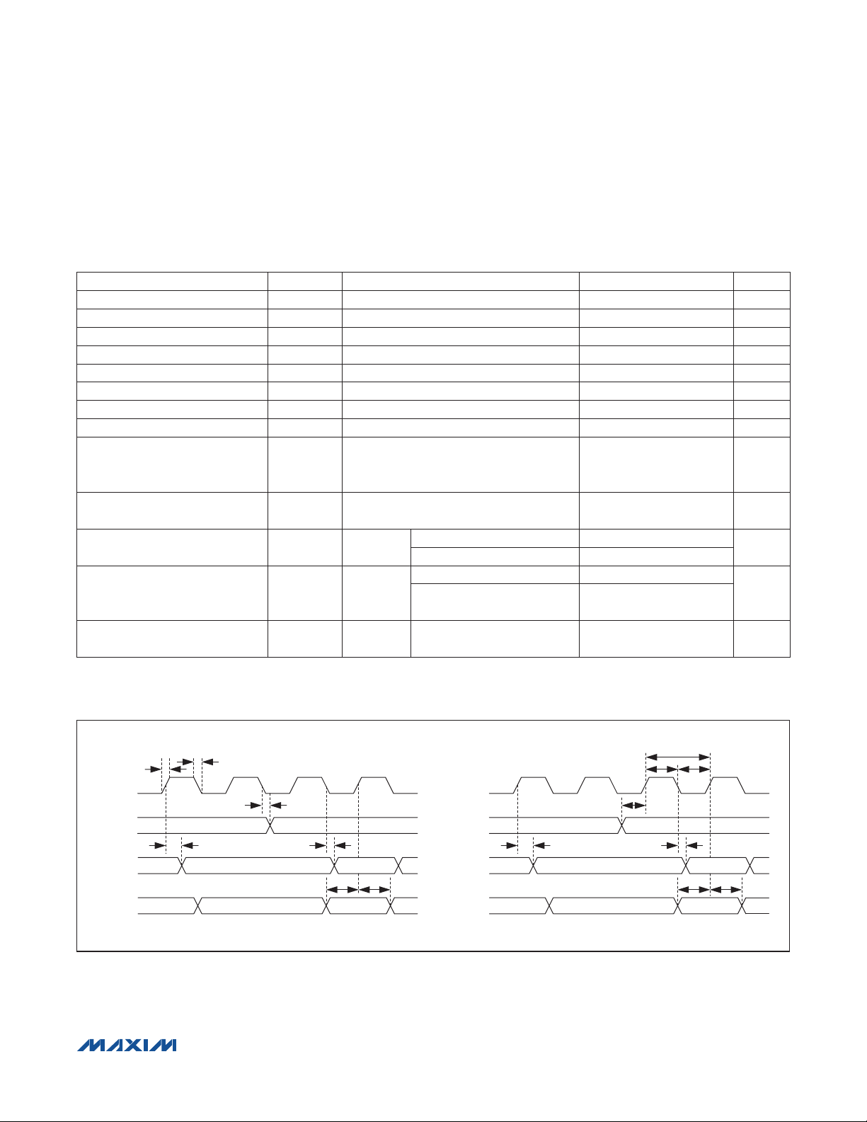
AUDIO INTERFACE TIMING CHARACTERISTICS
(V
= V
AVDD
(Note 1)
BCLK Cycle Time t
BCLK High Time t
BCLK Low Time t
BCLK or LRCLK Rise and Fall Time tR, t
SDIN to BCLK Setup Time t
LRCLK to BCLK Setup Time t
SDIN to BCLK Hold Time t
LRCLK to BCLK Hold Time t
Minimum Delay Time from LSB
BCLK Falling Edge to
High-Impedance State
LRCLK Rising Edge to SDOUT
MSB Delay
BCLK to SDOUT Delay t
Delay Time from BCLK to LRCLK t
Delay Time from LRCLK to BCLK
After LSB
PVDD
= V
DVDD
= V
DVDDS1
= V
DVDDS2
= +1.8V, V
SPKLVDD
PARAMETER SYMBOL CONDITIONS MIN TYP MAX UNITS
BCLK
BCLKH
BCLKL
SETUP
SYNCSET
HOLD
SYNCHOLD
t
HIZOUT
t
SYNCTXCL
CLKTX
CLKSYNC
t
ENDSYNC
Slave mode 90 ns
Slave mode 20 ns
Slave mode 20 ns
Master mode, CL = 15pF 5 ns
F
Slave mode 20 ns
Slave mode 20 ns
Master mode, TDM_ = 1 42 ns
= 30pF, TDM_ = 1, FSW_ = 1 50 ns
CL = 30pF
Master
mode
Master
mode
TDM_ = 1, BCLK rising edge 50
TDM_ = 0 50
TDM_ = 1 -15 +15
TDM_ = 0
TDM_ = 1, FSW_ = 1 20 ns
= V
MAX98088
Stereo Audio Codec
SPKRVDD
= 3.7V, TA = +25NC, unless otherwise noted.)
20 ns
20 ns
0.8 x
t
BCLKL
ns
ns
t
t
CLKSYNC
t
HIZOUT
F
t
CLKTX
HI-Z MSB
MASTER MODE
t
SETUPtHOLD
MSBLSB
BCLK
(OUTPUT)
LRCLK
(OUTPUT)
SDOUT
(OUTPUT)
SDIN
(INPUT)
t
R
LSB
Figure 1. Non-TDM Audio Interface Timing Diagrams (TDM_ = 0)
���������������������������������������������������������������� Maxim Integrated Products 22
BCLK
(INPUT)
LRCLK
(INPUT)
SDOUT
(OUTPUT)
SDIN
(INPUT)
t
SYNCSET
t
HIZOUT
LSB HI-Z
LSB
SLAVE MODE
t
BCLKH
t
CLKTX
t
BCLK
t
SETUPtHOLD
MSB
t
MSB
BCLKL
with FlexSound Technology
t
F
BCLK (OUTPUT)
t
CLKSYNC
LRCLK (OUTPUT)
t
t
SDOUT (OUTPUT)
SDIN (INPUT)
HIZOUT
LSB
CLKTX
HI-ZLSB
MASTER MODE SLAVE MODE
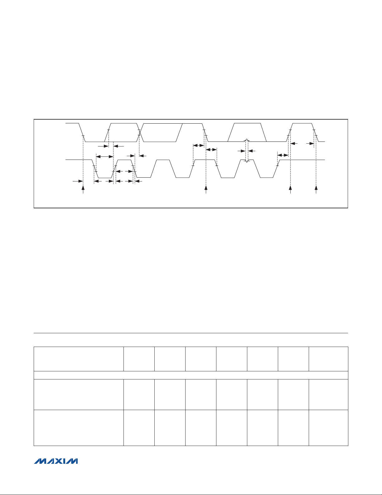
Figure 2. TDM Audio Interface Timing Diagram (TDM_ = 1, FSW_ = 0)
t
F
BCLK (OUTPUT)
t
ENDSYNC
LRCLK (OUTPUT)
t
SYNCTX
HI-ZLSB MSB
SDOUT (OUTPUT)
SDIN (INPUT)
t
HIZOUT
LSB MSB
t
R
t
CLKSYNC
MSB
MSB
t
R
t
CLKSYNC
t
CLKTX
t
SETUP
t
SETUP
t
HOLD
t
HOLD
SDOUT (OUTPUT)
SDOUT (OUTPUT)
BCLK (INPUT)
LRCLK (INPUT)
SDIN (INPUT)
BCLK (INPUT)
LRCLK (INPUT)
SDIN (INPUT)
MAX98088
Stereo Audio Codec
t
BCLK
t
SYNCSET
t
HIZOUT
t
HIZOUT
LSB
LSB
t
CLKTX
HI-ZLSB
t
SYNCTX
HI-ZLSB
t
BCLKH
t
SYNCHOLD
t
BCLKH
MSB
MSB
MSB
t
CLKTX
MSB
t
BCLK
t
SETUP
t
SETUP
t
BCLKL
t
HOLD
t
BCLKL
t
HOLD
MASTER MODE
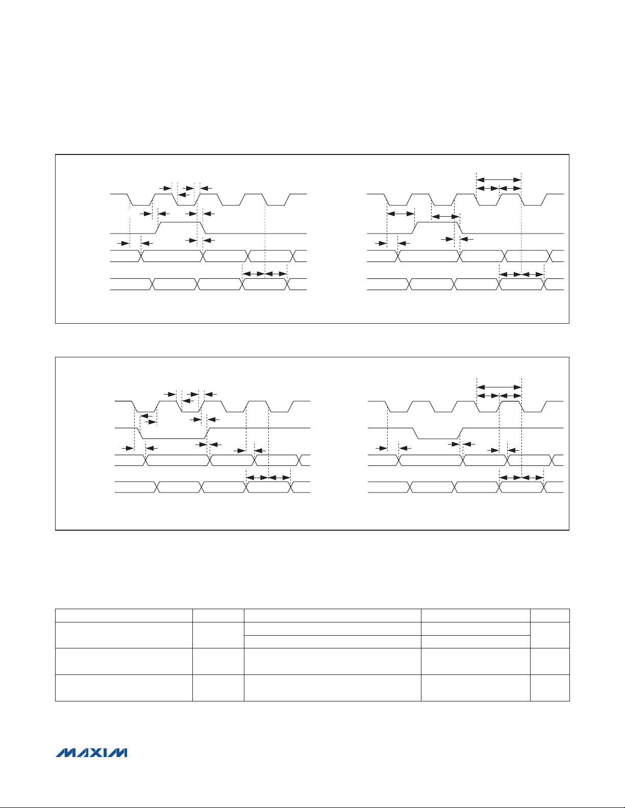
Figure 3. TDM Audio Interface Timing Diagram (TDM_ = 1, FSW_ = 1)
DIGITAL MICROPHONE TIMING CHARACTERSTICS
(V
= V
AVDD
(Note 1)
DIGMICCLK Frequency f
DIGMICDATA to DIGMICCLK
Setup Time
DIGMICDATA to DIGMICCLK
Hold Time
PVDD
= V
DVDD
= V
DVDDS1
= V
DVDDS2
= +1.8V, V
SPKLVDD
= V
PARAMETER SYMBOL CONDITIONS MIN TYP MAX UNITS
MICCLK
t
SU,MIC
t
HD,MIC
MICCLK = 00 MCLK/8
MICCLK = 01 MCLK/6
Either clock edge 20 ns
Either clock edge 0 ns
���������������������������������������������������������������� Maxim Integrated Products 23
SPKRVDD
SLAVE MODE
= 3.7V, TA = +25NC, unless otherwise noted.)
MHz
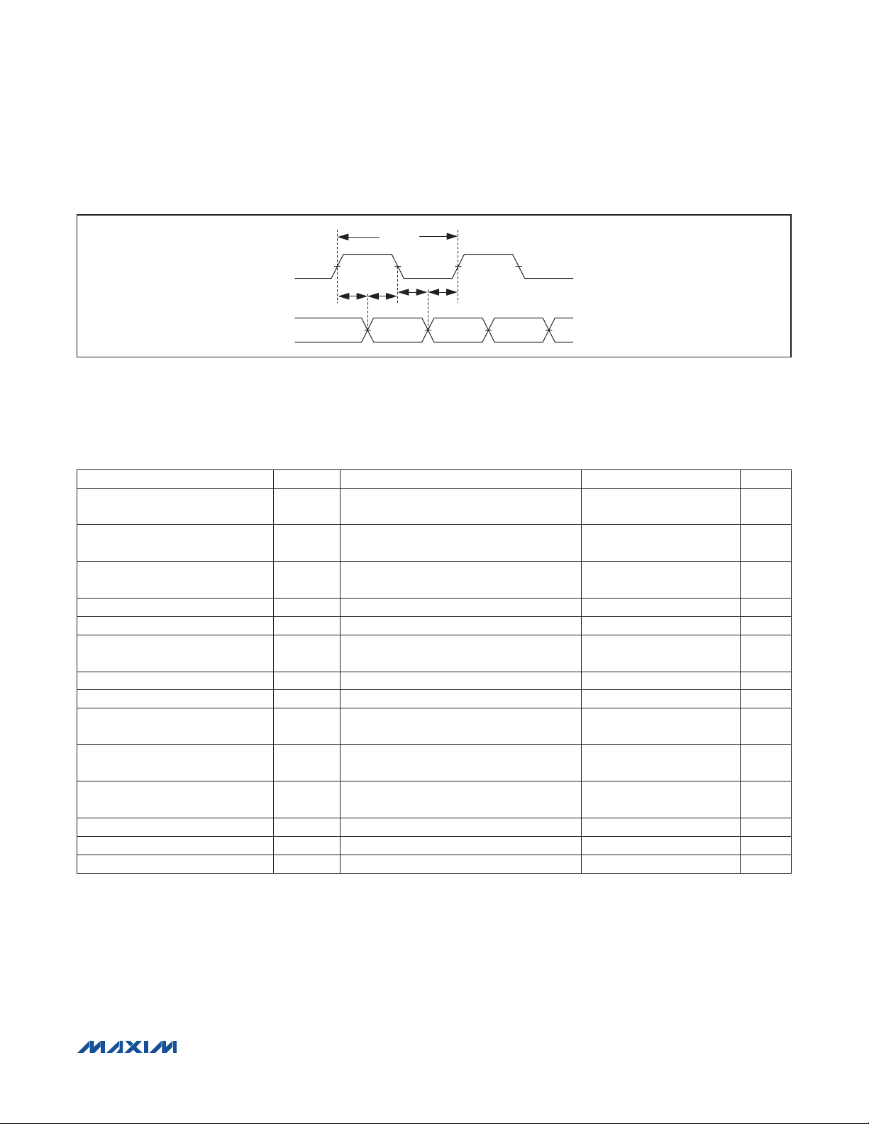
Figure 4. Digital Microphone Timing Diagram
I2C TIMING CHARACTERSTICS
(V
= V
AVDD
(Note 1)
Serial-Clock Frequency f
Bus Free Time Between STOP and
START Conditions
Hold Time (Repeated) START
Condition
SCL Pulse-Width Low t
SCL Pulse-Width High t
Setup Time for a Repeated START
Condition
Data Hold Time t
Data Setup Time t
SDA and SCL Receiving Rise Time t
SDA and SCL Receiving Fall Time t
SDA Transmitting Fall Time t
Setup Time for STOP Condition t
Bus Capacitance C
Pulse Width of Suppressed Spike t
PVDD
= V
DVDD
= V
DVDDS1
= V
DVDDS2
PARAMETER SYMBOL CONDITIONS MIN TYP MAX UNITS
SCL
t
BUF
t
HD,STA
LOW
HIGH
t
SU,STA
HD,DAT
SU,DAT
R
F
F
SU,STO
B
SP
MAX98088
Stereo Audio Codec
with FlexSound Technology
1/f
MICCLK
t
HD,MICtSU,MIC
t
HD,MICtSU,MIC
LEFT RIGHTLEFTRIGHT
= +1.8V, V
SPKLVDD
Guaranteed by SCL pulse-width low and
high
RPU = 475I, CB = 100pF, 400pF
(Note 10)
(Note 10)
RPU = 475I, CB = 100pF, 400pF (Note 10)
Guaranteed by SDA transmitting fall time 400 pF
= V
SPKRVDD
= 3.7V, TA = +25NC, unless otherwise noted.)
0 400 kHz
1.3
0.6
1.3
0.6
0.6
0 900 ns
100 ns
20 +
0.1C
20 +
0.1C
20 +
0.05C
B
B
B
300 ns
300 ns
250 ns
0.6
0 50 ns
Fs
Fs
Fs
Fs
Fs
Fs
���������������������������������������������������������������� Maxim Integrated Products 24
with FlexSound Technology
I2C TIMING CHARACTERISTICS (continued)
(V
AVDD
(Note 1)
= V
SDA
PVDD
= V
DVDD
= V
t
LOW
DVDDS1
t
SU,DAT
= V
DVDDS2
t
HD,DAT
= +1.8V, V
SPKLVDD
t
SU,STA
= V
MAX98088
Stereo Audio Codec
SPKRVDD
t
= 3.7V. TA = +25NC, unless otherwise noted.)
t
HD,STA
t
SP
t
SU,STO
BUF
SCL
t
HD,STA
START CONDITION
t
HIGH
t
t
R
F
REPEATED START CONDITION
STOP
CONDITION
START
CONDITION
Figure 5. I2C Interface Timing Diagram
Note 1: The IC is 100% production tested at TA = +25NC. Specifications over temperature limits are guaranteed by design.
Note 2: Analog supply current = I
+ I
DVDDS1
+ I
DVDDS2
.
AVDD
+ I
. Speaker supply current = I
HPVDD
SPKLVDD
+ I
SPKRVDD
. Digital supply current = I
DVDD
Note 3: Clocking all zeros into the DAC.
Note 4: Dynamic range measured using the EIAJ method. -60dBFS, 1kHz output signal, A-weighted and normalized to 0dBFS.
f = 20Hz to 20kHz.
Note 5: Gain measured relative to the 0dB setting.
Note 6: The filter specification is accurate only for synchronous clocking modes, where NI is a multiple of 0x1000.
Note 7: 0dBFS for DAC input. 1V
for INA/INB inputs.
P-P
Note 8: LRCLK may be any rate in the indicated range. Asynchronous or noninteger MCLK/LRCLK ratios may exhibit some full-
scale performance degradation compared to synchronous integer related MCLK/LRCLK ratios.
Note 9: In master-mode operation, the accuracy of the MCLK input proportionally determines the accuracy of the sample clock rate.
Note 10: CB is in pF.
Power Consumption
(V
AVDD
= V
PVDD
= V
DVDD
= V
DVDDS1
= V
DVDDS2
= 1.8V, V
SPKLVDD
= V
SPKRVDD
= 3.7V)
MODE
PLAYBACK TO HEADPHONE ONLY
DAC Playback 48kHz Stereo HP
DAC ª HP
Low power mode, 24-bit, music filters, 256Fs
DAC Playback 48kHz Stereo HP
DAC ª HP
Low power mode, 24-bit, music filters, 256Fs, 0.1mW/channel,
RHP = 32I
���������������������������������������������������������������� Maxim Integrated Products 25
I
AVDD
(mA)
I
PVDD
(mA)
I
SPKVDD
I
SPKLVDD
(mA)
+
I
DVDD
(mA)
I
DVDDS1
I
DVDDS2
(mA)
+
POWER
(mW)
DYNAMIC
RANGE (dB)
1.25 0.47 0.00 1.35 0.01 5.55 97
1.25 1.81 0.00 1.56 0.01 8.32 97
(V
= V
AVDD
DAC Playback 48kHz Stereo HP
DAC ª HP
24-bit, music filters, 256Fs
DAC Playback 48kHz Stereo HP
DAC ª HP
24-bit, music filters, 256Fs, 0.1mW/
channel, RHP = 32I
DAC Playback 44.1kHz Stereo HP
DAC ª HP
24-bit, music filters
DAC Playback 44.1kHz Stereo HP
DAC ª HP
Low power mode, 24-bit, music
filters
DAC Playback 8kHz Stereo HP
DAC ª HP
16-bit, voice filters
DAC Playback 8kHz Stereo HP
DAC ª HP
16-bit, low power mode, voice filters
DAC Playback 8kHz Mono HP
DAC ª HP
16-bit, low power mode, voice filters
Line Playback Stereo HP
INA ª HP
Single-ended inputs
DAC PLAYBACK TO CLASS D SPEAKER
DAC Playback 48kHz Stereo SPK
DAC ª SPK
24-bit, music filters
PVDD
= V
MODE
DVDD
= V
DVDDS1
= V
MAX98088
Stereo Audio Codec
with FlexSound Technology
Power Consumption (continued)
= 1.8V, V
DVDDS2
I
AVDD
(mA)
2.04 1.27 0.00 1.53 0.01 8.72 101
2.04 2.11 0.00 1.74 0.01 10.63 101
2.03 1.27 0.00 1.41 0.01 8.46 100
1.25 0.47 0.00 1.25 0.01 5.34 97
2.04 1.27 0.00 1.07 0.00 7.89 95
1.26 0.47 0.00 0.90 0.00 4.72 94
0.77 0.29 0.00 0.79 0.00 3.33 93.7
2.40 1.27 0.00 0.02 0.00 6.67 95
2.31 0.00 6.33 2.14 0.01 31.44 86
I
PVDD
(mA)
SPKLVDD
= V
I
SPKVDD
I
SPKLVDD
(mA)
SPKRVDD
+
= 3.7V)
I
DVDD
(mA)
I
DVDDS1
I
DVDDS2
(mA)
+
POWER
(mW)
DYNAMIC
RANGE (dB)
���������������������������������������������������������������� Maxim Integrated Products 26
(V
= V
AVDD
DAC Playback 48kHz Mono SPK
DAC ª SPK
24-bit, music filters
Line Playback Mono SPK
INA ª SPKL
Differential inputs
FULL DUPLEX
Full-Duplex 8kHz Mono RCV
MIC1 ª ADC
DAC ª REC
16-bit, voice filters
Full-Duplex 8kHz Stereo HP
MIC1/2 ª ADC
DAC ª HP
16-bit, mixer, voice filters
PVDD
= V
MODE
DVDD
= V
DVDDS1
MAX98088
Stereo Audio Codec
with FlexSound Technology
Power Consumption (continued)
= V
I
AVDD
(mA)
11.19 1.27 0.48 1.28 0.01 26.43
= 1.8V, V
DVDDS2
1.35 0.00 3.23 1.84 0.01 17.69 86
1.01 0.00 3.24 0.03 0.00 13.83 83
6.32 0.00 1.54 1.24 0.01 19.33
I
PVDD
(mA)
SPKLVDD
= V
I
SPKVDD
I
SPKLVDD
(mA)
SPKRVDD
+
= 3.7V)
I
DVDD
(mA)
I
DVDDS1
I
DVDDS2
(mA)
+
POWER
(mW)
DYNAMIC
RANGE (dB)
Record = 87
Playback = 94
Record = 87
Playback = 96
Full-Duplex 8kHz Stereo HP
MIC1/2 ª ADC
DAC ª HP
16-bit, low power mode, voice filters
LINE RECORD
Line Stereo Record 48kHz
INA ª ADC
24-bit, low power, music filters
Line Stereo Record 48kHz
INA ª ADC
Direct pin input, 24bit, low power,
music filters
7.12 0.47 0.48 1.10 0.02 17.44
6.19 0.00 0.20 1.31 0.15 14.47 91
5.69 0.00 0.20 1.31 0.12 13.53 93
Record = 87
Playback = 94
���������������������������������������������������������������� Maxim Integrated Products 27

(V
FREQUENCY (Hz)
AVDD
= V
PVDD
= V
DVDD
= V
DVDDS1
SPK_P and SPK_N. Receiver load (R
HPGND. RHP = J, R
= +20dB, AV
0dB, AV
MICPGA_
= 0dB, AV
REC
= J, Z
REC
= 0dB, AV
SPK
DACATTN
= 0dB, MCLK = 12.288MHz, LRCLK = 48kHz, MAS = 1. TA = +25NC, unless otherwise noted.)
SPK_
MAX98088
Stereo Audio Codec
with FlexSound Technology
Typical Operating Characteristics
= V
) connected between RECP and RECN. Headphone loads (RHP) connected from HPL or HPR to
REC
= J, C
REF
= 0dB, AV
DVDDS2
= 2.2FF, C
= +1.8V, V
MICBIAS
DACGAIN
SPKLVDD
= 0dB, AV
= C
= V
REG
= 1FF, C
ADCLVL
Microphone to ADC
SPKRVDD
C1N-C1P
= 0dB, AV
= 3.7V. Speaker loads (Z
= 1FF, C
ADCGAIN
= C
HPVDD
= 0dB, AV
) connected between
SPK
= 1FF. AV
HPVSS
= 0dB, AV
PGAIN_
MICPRE_
HP_
=
TOTAL HARMONIC DISTORTION PLUS
NOISE vs. FREQUENCY (MIC TO ADC)
0
MCLK = 13MHz
-10
LRCLK = 8kHz
-20
FREQ MODE
= 1V
V
IN
AV
MICPRE_
P-P
= 0dB
FREQUENCY (Hz)
100010010 10,000
-30
-40
-50
-60
THD+N RATIO (dB)
-70
-80
-90
-100
TOTAL HARMONIC DISTORTION PLUS
NOISE vs. FREQUENCY (MIC TO ADC)
0
MCLK = 12.288MHz
-10
LRCLK = 96kHz
-20
NI MODE
= 1V
V
IN
-30
-40
-50
-60
THD+N RATIO (dB)
-70
-80
-90
-100
P-P
AV
= 0dB
MICPRE_
10 100,000
FREQUENCY (Hz)
10,0001000100
MAX98088 toc01
MAX98088 toc04
TOTAL HARMONIC DISTORTION PLUS
NOISE vs. FREQUENCY (MIC TO ADC)
0
MCLK = 13MHz
-10
LRCLK = 44.1kHz
PLL MODE
-20
= 1V
V
IN
-30
-40
-50
THD+N RATIO (dB)
-60
-70
-80
-90
P-P
AV
= 0dB
MICPRE_
10 100,000
FREQUENCY (Hz)
10,0001000100
TOTAL HARMONIC DISTORTION PLUS
NOISE vs. FREQUENCY (MIC TO ADC)
0
MCLK = 13MHz
-10
LRCLK = 8kHz
-20
FREQ MODE
= 0.1V
V
IN
AV
MICPRE_
P-P
= 0dB
FREQUENCY (Hz)
100010010 10,000
-30
-40
-50
-60
THD+N RATIO (dB)
-70
-80
-90
-100
MAX98088 toc02
THD+N RATIO (dB)
MAX98088 toc05
THD+N RATIO (dB)
TOTAL HARMONIC DISTORTION PLUS
NOISE vs. FREQUENCY (MIC TO ADC)
0
MCLK = 12.288MHz
-10
LRCLK = 48kHz
-20
NI MODE
= 1V
V
IN
-30
-40
-50
-60
-70
-80
-90
-100
P-P
AV
= 0dB
MICPRE_
10 100,000
10,0001000100
TOTAL HARMONIC DISTORTION PLUS
NOISE vs. FREQUENCY (MIC TO ADC)
0
MCLK = 13MHz
-10
LRCLK = 8kHz
-20
FREQ MODE
= 0.032V
V
IN
MICPRE_
P-P
= 0dB
FREQUENCY (Hz)
100010010 10,000
-30
-40
-50
-60
-70
-80
-90
-100
AV
MAX98088 toc03
MAX98088 toc06
���������������������������������������������������������������� Maxim Integrated Products 28
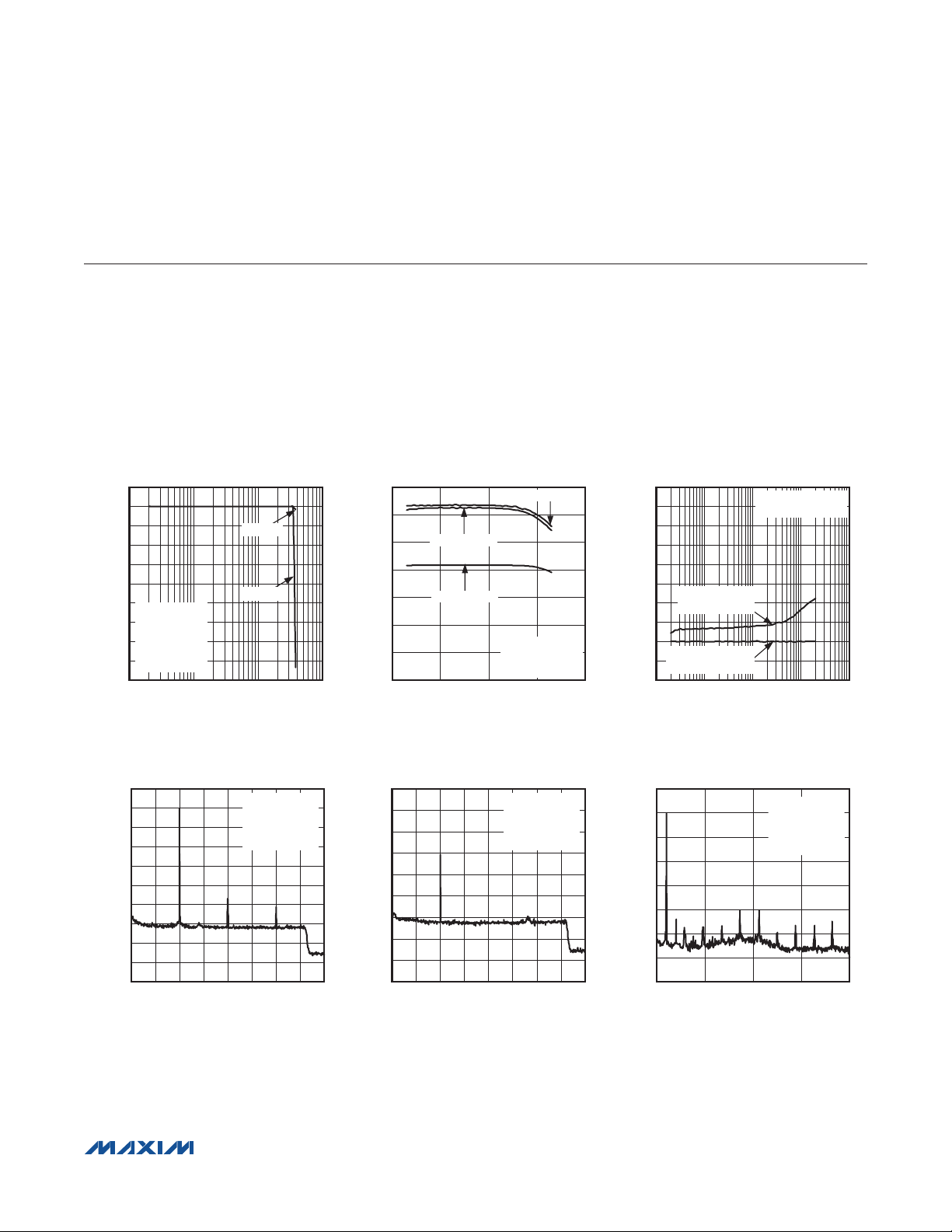
(V
AVDD
= V
PVDD
= V
DVDD
= V
DVDDS1
SPK_P and SPK_N. Receiver load (R
HPGND. RHP = J, R
= +20dB, AV
0dB, AV
MICPGA_
= 0dB, AV
REC
= J, Z
REC
= 0dB, AV
SPK
DACATTN
= 0dB, MCLK = 12.288MHz, LRCLK = 48kHz, MAS = 1. TA = +25NC, unless otherwise noted.)
SPK_
MAX98088
Stereo Audio Codec
with FlexSound Technology
Typical Operating Characteristics (continued)
= V
) connected between RECP and RECN. Headphone loads (RHP) connected from HPL or HPR to
REC
= J, C
REF
= 0dB, AV
DVDDS2
= 2.2FF, C
= +1.8V, V
MICBIAS
DACGAIN
SPKLVDD
= C
REG
= 0dB, AV
= V
SPKRVDD
= 1FF, C
ADCLVL
= 3.7V. Speaker loads (Z
C1N-C1P
= 0dB, AV
= 1FF, C
ADCGAIN
HPVDD
= C
= 0dB, AV
) connected between
SPK
= 1FF. AV
HPVSS
= 0dB, AV
PGAIN_
MICPRE_
HP_
=
GAIN vs. FREQUENCY (MIC TO ADC)
10
0
-10
-20
-30
-40
-50
MCLK = 13MHz
-60
NORMALIZED GAIN (dB)
LRCLK = 8kHz
FREQ MODE
-70
V
= 1V
IN
AV
P-P
MICPRE_
-80
-90
= 0dB
FREQUENCY (Hz)
MODE = 1
MODE = 0
100010010 10k
FFT, 0dBFS (MIC TO ADC)
20
0
-20
-40
-60
-80
-100
AMPLITUDE (dBFS)
-120
-140
-160
-180
0 4000
FREQUENCY (Hz)
MCLK = 13MHz
AV
LRCLK = 8kHz
FREQ MODE
= 0dB
MICPRE_
350030002000 25001000 1500500
MAX98088 toc07
CMRR (dB)
MAX98088 toc10
-100
AMPLITUDE (dBFS)
-120
-140
-160
-180
COMMON-MODE REJECTION RATIO
vs. FREQUENCY (MIC TO ADC)
70
60
50
40
30
20
10
0
MICPRE = 20dB
MICPRE = 0dB
10 100,000
FREQUENCY (Hz)
MICPRE = 30dB
MCLK = 12.288MHz
LRCLK = 48kHz
FREQ MODE
10,0001000100
FFT, -60dBFS (MIC TO ADC)
0
-20
-40
-60
-80
FREQUENCY (Hz)
MCLK = 13MHz
LRCLK = 8kHz
FREQ MODE
AV
MICPRE_
= 0dB
350030002000 25001000 15005000 4000
MAX98088 toc08
PSRR (dB)
MAX98088 toc11
AMPLITUDE (dBFS)
POWER-SUPPLY RECTION RATIO
vs. FREQUENCY (MIC TO ADC)
10
0
-10
-20
-30
-40
-50
-60
-70
-80
-90
RIPPLE ON AVDD,
DVDD, HPVDD
RIPPLE ON SPKLVDD,
10 100,000
INPUTS AC GROUNDED
SPKRVDD
FREQUENCY (Hz)
V
RIPPLE
= 200mV
10,0001000100
FFT, 0dBFS (MIC TO ADC)
20
0
-20
-40
-60
-80
-100
-120
-140
0 20,000
FREQUENCY (Hz)
MCLK = 13MHz
LRCLK = 44.1kHz
PLL MODE
AV
MICPRE_
15,00010,0005000
P-P
MAX98088 toc09
MAX98088 toc12
= 0dB
���������������������������������������������������������������� Maxim Integrated Products 29
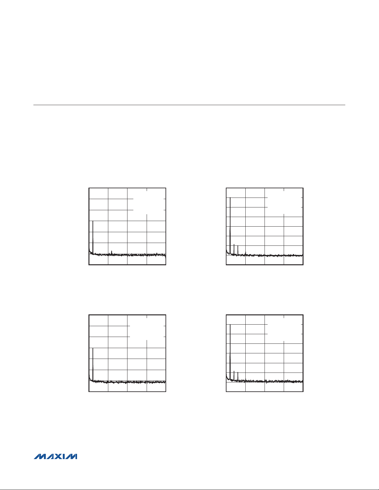
(V
02
02
02
02
AVDD
= V
PVDD
= V
DVDD
= V
DVDDS1
SPK_P and SPK_N. Receiver load (R
HPGND. RHP = J, R
= +20dB, AV
0dB, AV
MICPGA_
= 0dB, AV
REC
= J, Z
REC
= 0dB, AV
SPK
DACATTN
= 0dB, MCLK = 12.288MHz, LRCLK = 48kHz, MAS = 1. TA = +25NC, unless otherwise noted.)
SPK_
MAX98088
Stereo Audio Codec
with FlexSound Technology
Typical Operating Characteristics (continued)
= V
) connected between RECP and RECN. Headphone loads (RHP) connected from HPL or HPR to
REC
= J, C
REF
= 0dB, AV
DVDDS2
= 2.2FF, C
= +1.8V, V
MICBIAS
DACGAIN
SPKLVDD
= C
REG
= 0dB, AV
= V
SPKRVDD
= 1FF, C
ADCLVL
= 3.7V. Speaker loads (Z
C1N-C1P
= 0dB, AV
= 1FF, C
ADCGAIN
HPVDD
= C
= 0dB, AV
) connected between
SPK
= 1FF. AV
HPVSS
= 0dB, AV
PGAIN_
MICPRE_
HP_
=
FFT, -60dBFS (MIC TO ADC)
0
-20
-40
-60
-80
AMPLITUDE (dBFS)
-100
-120
-140
FFT, -60dBFS (MIC TO ADC)
0
-20
-40
-60
-80
AMPLITUDE (dBFS)
-100
-120
-140
LRCLK = 44.1kHz
AV
FREQUENCY (kHz)
MCLK = 12.288MHz
AV
FREQUENCY (kHz)
MCLK = 13MHz
PLL MODE
= 0dB
MICPRE_
15105
LRCLK = 48kHz
NI MODE
= 0dB
MICPRE_
15105
MAX98088 toc13
0
MAX98088 toc15
0
20
0
-20
-40
-60
-80
AMPLITUDE (dBFS)
-100
-120
-140
20
0
-20
-40
-60
-80
AMPLITUDE (dBFS)
-100
-120
-140
FFT, 0dBFS (MIC TO ADC)
MCLK = 12.288MHz
LRCLK = 48kHz
NI MODE
AV
MICPRE_
1515
FREQUENCY (kHz)
FFT, 0dBFS (MIC TO ADC)
MCLK = 12.288MHz
LRCLK = 96kHz
NI MODE
AV
MICPRE_
15105
FREQUENCY (kHz)
MAX98088 toc14
= 0dB
0
MAX98088 toc16
= 0dB
0
���������������������������������������������������������������� Maxim Integrated Products 30

(V
02
AVDD
= V
PVDD
= V
DVDD
= V
DVDDS1
SPK_P and SPK_N. Receiver load (R
HPGND. RHP = J, R
= +20dB, AV
0dB, AV
MICPGA_
= 0dB, AV
REC
= J, Z
REC
= 0dB, AV
SPK
DACATTN
= 0dB, MCLK = 12.288MHz, LRCLK = 48kHz, MAS = 1. TA = +25NC, unless otherwise noted.)
SPK_
MAX98088
Stereo Audio Codec
with FlexSound Technology
Typical Operating Characteristics (continued)
= V
) connected between RECP and RECN. Headphone loads (RHP) connected from HPL or HPR to
REC
= J, C
REF
= 0dB, AV
DVDDS2
= 2.2FF, C
= +1.8V, V
MICBIAS
DACGAIN
SPKLVDD
= C
REG
= 0dB, AV
= V
SPKRVDD
= 1FF, C
ADCLVL
= 3.7V. Speaker loads (Z
C1N-C1P
= 0dB, AV
= 1FF, C
ADCGAIN
HPVDD
= C
= 0dB, AV
) connected between
SPK
= 1FF. AV
HPVSS
= 0dB, AV
PGAIN_
MICPRE_
HP_
=
FFT, -60dBFS (MIC TO ADC)
0
-20
-40
-60
-80
AMPLITUDE (dBFS)
-100
-120
-140
MCLK = 12.288MHz
AV
FREQUENCY (kHz)
LRCLK = 96kHz
NI MODE
MICPRE_
15105
MAX98088 toc17
= 0dB
0
SOFTWARE TURN-ON/OFF RESPONSE
(MIC TO ADC)
ADC ENABLE/DISABLE RESPONSE
(MIC TO ADC)
10ms/div
MAX98088 toc19
SCL
1V/div
MAX98088 toc18
SCL
1V/div
ADC
OUTPUT
0.5V/div
���������������������������������������������������������������� Maxim Integrated Products 31
ADC
OUTPUT
0.5V/div
10ms/div

(V
AVDD
= V
PVDD
= V
DVDD
= V
DVDDS1
SPK_P and SPK_N. Receiver load (R
HPGND. RHP = J, R
= +20dB, AV
0dB, AV
MICPGA_
= 0dB, AV
REC
= J, Z
REC
= 0dB, AV
SPK
DACATTN
= 0dB, MCLK = 12.288MHz, LRCLK = 48kHz, MAS = 1. TA = +25NC, unless otherwise noted.)
SPK_
MAX98088
Stereo Audio Codec
with FlexSound Technology
Typical Operating Characteristics (continued)
= V
) connected between RECP and RECN. Headphone loads (RHP) connected from HPL or HPR to
REC
= J, C
REF
= 0dB, AV
DVDDS2
= 2.2FF, C
= +1.8V, V
MICBIAS
DACGAIN
Line to ADC
SPKLVDD
= C
REG
= 0dB, AV
= V
SPKRVDD
= 1FF, C
ADCLVL
= 3.7V. Speaker loads (Z
C1N-C1P
= 0dB, AV
= 1FF, C
ADCGAIN
HPVDD
= C
= 0dB, AV
) connected between
SPK
= 1FF. AV
HPVSS
= 0dB, AV
PGAIN_
MICPRE_
HP_
=
TOTAL HARMONIC DISTORTION PLUS NOISE
vs. FREQUENCY (LINE TO ADC)
0
-10
-20
-30
-40
-50
THD+N RATIO (dB)
-60
-70
-80
-90
10 100,000
FREQUENCY (Hz)
MCLK = 12.288MHz
LRCLK = 48kHz
V
IN
AV
PGAIN_
10,0001000100
TOTAL HARMONIC DISTORTION PLUS NOISE
vs. FREQUENCY (LINE-IN TO ADC)
0
-10
-20
-30
-40
-50
THD+N (dB)
-60
-70
-80
-90
10 100,000
NI MODE
= 1.4V
C
FREQUENCY (Hz)
MAX98088 toc20
P-P
= -6dB
= 1µF
IN
MCLK = 12.288MHz
EXTERNAL GAIN MODE
TOTAL HARMONIC DISTORTION PLUS NOISE
vs. FREQUENCY (LINE TO ADC)
0
-10
-20
-30
-40
-50
-60
THD+N RATIO (dB)
-70
-80
-90
-100
10 100,000
FREQUENCY (Hz)
LRCLK = 48kHz
VIN = 1V
RMS
MAX98088 toc23
= 56kI
R
IN
C
= 1µF
IN
10,0001000100
MCLK = 12.288MHz
AV
TOTAL HARMONIC DISTORTION PLUS NOISE
vs. FREQUENCY (LINE TO ADC)
0
LRCLK = 48kHz
NI MODE
V
= 1V
IN
= 0dB
PGAIN_
C
= 1µF
IN
10,0001000100
P-P
MAX98088 toc21
-10
-20
-30
-40
-50
THD+N RATIO (dB)
-60
-70
-80
-90
10 100,000
POWER-SUPPLY REJECTION RATIO
vs. FREQUENCY (LINE-IN TO ADC)
10
0
-10
-20
-30
-40
PSRR (dB)
-50
-60
-70
-80
-90
RIPPLE ON AVDD,
DVDD, HPVDD
RIPPLE ON SPKLVDD,
SPKRVDD
10 100,000
FREQUENCY (Hz)
V
RIPPLE
FREQUENCY (Hz)
= 200mV
10,0001000100
MCLK = 12.288MHz
AV
P-P
MAX98088 toc24
LRCLK = 48kHz
NI MODE
V
= 0.1V
IN
= +20dB
PGAIN_
C
= 1µF
IN
10,0001000100
P-P
MAX98088 toc22
���������������������������������������������������������������� Maxim Integrated Products 32

(V
02
02
AVDD
= V
PVDD
= V
DVDD
= V
DVDDS1
SPK_P and SPK_N. Receiver load (R
HPGND. RHP = J, R
= +20dB, AV
0dB, AV
MICPGA_
= 0dB, AV
REC
= J, Z
REC
= 0dB, AV
SPK
DACATTN
= 0dB, MCLK = 12.288MHz, LRCLK = 48kHz, MAS = 1. TA = +25NC, unless otherwise noted.)
SPK_
MAX98088
Stereo Audio Codec
with FlexSound Technology
Typical Operating Characteristics (continued)
= V
) connected between RECP and RECN. Headphone loads (RHP) connected from HPL or HPR to
REC
= J, C
REF
= 0dB, AV
= +1.8V, V
DVDDS2
= 2.2FF, C
DACGAIN
SPKLVDD
MICBIAS
= 0dB, AV
= C
REG
Line-In Pin Direct to ADC
= V
SPKRVDD
= 1FF, C
ADCLVL
= 3.7V. Speaker loads (Z
C1N-C1P
= 0dB, AV
= 1FF, C
ADCGAIN
HPVDD
= C
= 0dB, AV
) connected between
SPK
= 1FF. AV
HPVSS
= 0dB, AV
PGAIN_
MICPRE_
HP_
=
TOTAL HARMONIC DISTORTION PLUS NOISE
vs. FREQUENCY (LINE-IN DIRECT TO ADC)
0
-10
-20
-30
-40
-50
-60
THD+N RATIO (dB)
-70
-80
-90
-100
10 100,000
FREQUENCY (Hz)
MCLK = 12.288MHz
LRCLK = 48kHz
V
10,0001000100
FFT, 0dBFS (SDINS1 TO SDINS2
DIGITAL LOOPBACK)
0
-20
-40
-60
-80
-100
AMPLITUDE (dBFS)
-120
-140
-160
-180
FREQUENCY (kHz)
MCLK = 12.288MHz
LRCLK = 48kHz
15105
NI MODE
IN
CIN = 1µF
= 1V
P-P
MAX98088 toc25
Digital Loopback
NI MODE
MAX98088 toc27
0
POWER-SUPPLY REJECTION RATIO
vs. FREQUENCY (LINE-IN DIRECT TO ADC)
0
-10
-20
-30
RIPPLE ON AVDD,
-40
-50
PSRR (dB)
-60
-70
-80
-90
DVDD, HPVDD
RIPPLE ON SPKLVDD, SPKRVDD
10 100,000
FREQUENCY (Hz)
V
RIPPLE
10,0001000100
FFT, -60dBFS (SDINS1 TO SDINS2
DIGITAL LOOPBACK)
0
-20
-40
-60
-80
-100
AMPLITUDE (dBFS)
-120
-140
-160
-180
FREQUENCY (kHz)
MCLK = 12.288MHz
LRCLK = 48kHz
= 200mV
NI MODE
15105
P-P
MAX98088 toc26
MAX98088 toc28
0
���������������������������������������������������������������� Maxim Integrated Products 33

(V
02
02
02
02
AVDD
= V
PVDD
= V
DVDD
= V
DVDDS1
SPK_P and SPK_N. Receiver load (R
HPGND. RHP = J, R
= +20dB, AV
0dB, AV
MICPGA_
= 0dB, AV
REC
= J, Z
REC
= 0dB, AV
SPK
DACATTN
= 0dB, MCLK = 12.288MHz, LRCLK = 48kHz, MAS = 1. TA = +25NC, unless otherwise noted.)
SPK_
MAX98088
Stereo Audio Codec
with FlexSound Technology
Typical Operating Characteristics (continued)
= V
) connected between RECP and RECN. Headphone loads (RHP) connected from HPL or HPR to
REC
= J, C
REF
= 0dB, AV
DVDDS2
= 2.2FF, C
= +1.8V, V
DACGAIN
SPKLVDD
MICBIAS
= 0dB, AV
= C
REG
Analog Loopback
= V
SPKRVDD
= 1FF, C
ADCLVL
= 3.7V. Speaker loads (Z
C1N-C1P
= 0dB, AV
= 1FF, C
ADCGAIN
HPVDD
= C
= 0dB, AV
) connected between
SPK
= 1FF. AV
HPVSS
= 0dB, AV
PGAIN_
MICPRE_
HP_
=
TOTAL HARMONIC DISTORTION PLUS
NOISE vs. FREQUENCY
(LINE TO ADC TO DAC TO HEADPHONE)
0
MCLK = 13MHz
-10
LRCLK = 44.1kHz
PLL MODE
-20
RHP = 32I
-30
C
= 1µF
IN
-40
-50
THD+N RATIO (dB)
-60
P
= 0.020W
OUT
-70
-80
-90
10 100,000
P
= 0.01W
OUT
FREQUENCY (Hz)
10,0001000100
FFT, -60dBFS (LINE TO ADC TO DAC
TO HEADPHONE)
0
-20
-40
-60
-80
AMPLITUDE (dBV)
-100
-120
-140
FREQUENCY (kHz)
MCLK = 13MHz
LRCLK = 44.1kHz
PLL MODE
= 32I
R
HP
C
= 1µF
IN
15105
MAX98088 toc29
MAX98088 toc32
0
TOTAL HARMONIC DISTORTION PLUS
NOISE vs. FREQUENCY
(LINE TO ADC TO DAC TO HEADPHONE)
0
MCLK = 12.288MHz
-10
LRCLK = 48kHz
NI MODE
-20
-30
-40
-50
THD+N RATIO (dB)
-60
-70
-80
P
R
C
OUT
= 32I
HP
= 1µF
IN
= 0.01W
P
OUT
= 0.020W
FREQUENCY (Hz)
FFT, 0dBFS (LINE TO ADC TO DAC
TO HEADPHONE)
20
0
-20
-40
-60
-80
AMPLITUDE (dBV)
-100
-120
-140
MCLK = 12.288MHz
FREQUENCY (kHz)
10,000100010010 100,000
LRCLK = 48kHz
NI MODE
= 32I
R
HP
C
= 1µF
IN
15105
MAX98088 toc30
MAX98088 toc33
0
FFT, 0dBFS (LINE TO ADC TO DAC
TO HEADPHONE)
20
0
-20
-40
-60
-80
AMPLITUDE (dBV)
-100
-120
-140
FREQUENCY (kHz)
FFT, -60dBFS (LINE TO ADC TO DAC
TO HEADPHONE)
0
-20
-40
-60
-80
AMPLITUDE (dBV)
-100
-120
-140
FREQUENCY (kHz)
MCLK = 13MHz
LRCLK = 44.1kHz
PLL MODE
= 32I
R
HP
C
= 1µF
IN
15105
MCLK = 12.288MHz
LRCLK = 48kHz
NI MODE
= 32I
R
HP
C
= 1µF
IN
15105
MAX98088 toc31
0
MAX98088 toc34
0
���������������������������������������������������������������� Maxim Integrated Products 34

(V
AVDD
= V
PVDD
= V
DVDD
= V
DVDDS1
SPK_P and SPK_N. Receiver load (R
HPGND. RHP = J, R
= +20dB, AV
0dB, AV
MICPGA_
= 0dB, AV
REC
= J, Z
REC
= 0dB, AV
SPK
DACATTN
= 0dB, MCLK = 12.288MHz, LRCLK = 48kHz, MAS = 1. TA = +25NC, unless otherwise noted.)
SPK_
MAX98088
Stereo Audio Codec
with FlexSound Technology
Typical Operating Characteristics (continued)
= V
) connected between RECP and RECN. Headphone loads (RHP) connected from HPL or HPR to
REC
= J, C
REF
= 0dB, AV
DVDDS2
= 2.2FF, C
= +1.8V, V
DACGAIN
SPKLVDD
MICBIAS
= 0dB, AV
= C
DAC to Receiver
= V
REG
SPKRVDD
= 1FF, C
ADCLVL
= 3.7V. Speaker loads (Z
C1N-C1P
= 0dB, AV
= 1FF, C
ADCGAIN
HPVDD
= C
= 0dB, AV
) connected between
SPK
= 1FF. AV
HPVSS
= 0dB, AV
PGAIN_
MICPRE_
HP_
=
TOTAL HARMONIC DISTORTION PLUS NOISE
vs. OUTPUT POWER (DAC TO RECEIVER)
0
MCLK = 13MHz
-10
LRCLK = 8kHz
FREQ MODE
-20
R
= 32I
REC
= +8dB
AV
REC
-30
-40
-50
THD+N (dB)
-60
-70
-80
-90
f = 1000Hz
0 0.12
f = 3000Hz
f = 100Hz
OUTPUT POWER (W)
GAIN vs. FREQUENCY
(DAC TO RECEIVER)
5
MCLK = 13MHz
4
LRCLK = 8kHz
3
FREQ MODE
= 32I
R
REC
2
1
0
-1
-2
NORMALIZED GAIN (dB)
-3
-4
-5
FREQUENCY (Hz)
TOTAL HARMONIC DISTORTION PLUS NOISE
vs. FREQUENCY (DAC TO RECEIVER)
0
MCLK = 13MHz
-10
LRCLK = 8kHz
MAX98088 toc35
0.100.080.060.040.02
FREQ MODE
-20
R
= 32I
REC
= +8dB
AV
REC
-30
-40
-50
THD+N (dB)
-60
-70
-80
-90
10 10,000
P
= 0.02W
OUT
FREQUENCY (Hz)
P
OUT
1000100
MAX98088 toc36
= 0.08W
POWER CONSUMPTION vs. OUTPUT
POWER (DAC TO RECEIVER)
250
MCLK = 13MHz
MAX98088 toc38
10,000100010010
LRCLK = 8kHz
200
FREQ MODE
AV
= +8dB
REC
R
= 32I
REC
150
100
POWER CONSUMPTION (mW)
50
0
0 120
OUTPUT POWER PER CHANNEL (mW)
MAX98088 toc39
10080604020
OUTPUT POWER vs. SUPPLY VOLTAGE
(DAC TO RECEIVER)
200
MCLK = 13MHz
180
LRCLK = 8kHz
FREQ MODE
= 32I
R
160
REC
AV
= +8dB
REC
140
120
100
OUTPUT POWER PER CHANNEL (mW)
80
60
2.5 5.5
THD+N = 10%
THD+N = 1%
SUPPLY VOLTAGE (V)
POWER-SUPPLY REJECTION RATIO
vs. FREQUENCY (DAC TO RECEIVER)
0
-10
-20
-30
-40
RIPPLE ON AVDD,
-50
PSRR (dB)
-60
-70
-80
-90
-100
DVDD, HPVDD
RIPPLE ON SPKLVDD,
10 100,000
INPUTS AC GROUNDED
V
RIPPLE
SPKRVDD
FREQUENCY (Hz)
10,0001000100
5.04.54.03.53.0
= 200mV
MAX98088 toc37
P-P
MAX98088 toc40
���������������������������������������������������������������� Maxim Integrated Products 35

(V
02
02
AVDD
= V
PVDD
= V
DVDD
= V
DVDDS1
SPK_P and SPK_N. Receiver load (R
HPGND. RHP = J, R
= +20dB, AV
0dB, AV
MICPGA_
= 0dB, AV
REC
= J, Z
REC
= 0dB, AV
SPK
DACATTN
= 0dB, MCLK = 12.288MHz, LRCLK = 48kHz, MAS = 1. TA = +25NC, unless otherwise noted.)
SPK_
MAX98088
Stereo Audio Codec
with FlexSound Technology
Typical Operating Characteristics (continued)
= V
) connected between RECP and RECN. Headphone loads (RHP) connected from HPL or HPR to
REC
= J, C
REF
= 0dB, AV
DVDDS2
= 2.2FF, C
= +1.8V, V
MICBIAS
DACGAIN
SPKLVDD
= C
REG
= 0dB, AV
= V
SPKRVDD
= 1FF, C
ADCLVL
= 3.7V. Speaker loads (Z
C1N-C1P
= 0dB, AV
= 1FF, C
ADCGAIN
HPVDD
= C
= 0dB, AV
) connected between
SPK
= 1FF. AV
HPVSS
= 0dB, AV
PGAIN_
MICPRE_
HP_
=
SOFTWARE TURN-ON/OFF RESPONSE
(DAC TO RECEIVER, VSEN = 0)
10ms/div
FFT, -60dBFS (DAC TO RECEIVER)
0
-20
-40
-60
-80
AMPLITUDE (dBV)
-100
-120
MAX98088 toc41
MCLK = 13MHz
LRCLK = 8kHz
FREQ MODE
= 32I
R
REC
SCL
1V/div
RECEIVER
OUTPUT
1V/div
-20
MAX98088 toc44
-40
-60
AMPLITUDE (dBm)
-80
-100
SOFTWARE TURN-ON/OFF RESPONSE
(DAC TO RECEIVER, VSEN = 1)
10ms/div
WIDEBAND FFT, 0dBFS
(DAC TO RECEIVER)
0
MCLK = 13MHz
LRCLK = 8kHz
MAX98088 toc42
FREQ MODE
= 32I
R
REC
SCL
1V/div
RECEIVER
OUTPUT
1V/div
MAX98088 toc45
FFT, 0dBFS (DAC TO RECEIVER)
20
0
-20
-40
-60
-80
AMPLITUDE (dBV)
-100
-120
-140
-160
0
-20
-40
-60
AMPLITUDE (dBm)
-80
-100
MCLK = 13MHz
LRCLK = 8kHz
FREQ MODE
R
15105
FREQUENCY (kHz)
WIDEBAND FFT, 0dBFS
(DAC TO RECEIVER)
MCLK = 13MHz
LRCLK = 8kHz
FREQ MODE
R
REC
REC
= 32I
= 32I
MAX16067 toc43
0
MAX98088 toc46
-140
15105
FREQUENCY (kHz)
-120
0
0 10,000
���������������������������������������������������������������� Maxim Integrated Products 36
FREQUENCY (kHz)
1000100101
-120
0 10,000
FREQUENCY (kHz)
1000100101

(V
FREQUENCY (Hz)
AVDD
= V
PVDD
= V
DVDD
= V
DVDDS1
SPK_P and SPK_N. Receiver load (R
HPGND. RHP = J, R
= +20dB, AV
0dB, AV
MICPGA_
= 0dB, AV
REC
= J, Z
REC
= 0dB, AV
SPK
DACATTN
= 0dB, MCLK = 12.288MHz, LRCLK = 48kHz, MAS = 1. TA = +25NC, unless otherwise noted.)
SPK_
MAX98088
Stereo Audio Codec
with FlexSound Technology
Typical Operating Characteristics (continued)
= V
) connected between RECP and RECN. Headphone loads (RHP) connected from HPL or HPR to
REC
= J, C
REF
= 0dB, AV
DVDDS2
= 2.2FF, C
= +1.8V, V
DACGAIN
SPKLVDD
MICBIAS
= 0dB, AV
= C
Line to Receiver
= V
REG
SPKRVDD
= 1FF, C
ADCLVL
= 3.7V. Speaker loads (Z
C1N-C1P
= 0dB, AV
= 1FF, C
ADCGAIN
HPVDD
= C
= 0dB, AV
) connected between
SPK
= 1FF. AV
HPVSS
= 0dB, AV
PGAIN_
MICPRE_
HP_
=
TOTAL HARMONIC DISTORTION PLUS NOISE
vs. OUTPUT POWER (LINE TO RECEIVER)
0
R
= 32I
REC
AV
= +8dB
REC
-10
= 1µF
C
IN
-20
-30
-40
THD+N RATIO (dB)
-50
-60
-70
f = 100Hz
0 0.10
f = 1000Hz
OUTPUT POWER (W)
f = 6000Hz
GAIN vs. FREQUENCY
(LINE TO RECEIVER)
5
R
= 32I
REC
4
= 1µF
C
IN
3
2
1
0
-1
-2
NORMALIZED GAIN (dB)
-3
-4
-5
10 100,000
FREQUENCY (Hz)
10,0001000100
TOTAL HARMONIC DISTORTION PLUS NOISE
vs. FREQUENCY (LINE TO RECEIVER)
0
R
= 32I
REC
-10
AV
= +8dB
REC
= 1µF
C
MAX98088 toc47
0.080.060.040.02
IN
-20
-30
-40
-50
THD+N RATIO (dB)
-60
-70
-80
-90
10 100,000
P
= 0.02W
OUT
P
= 0.08W
OUT
FREQUENCY (Hz)
10,0001000100
MAX98088 toc48
POWER-SUPPLY
REJECTION RATIO vs. FREQUENCY
(LINE-IN DIRECT TO RECEIVER)
MAX98088 toc49
0
-10
-20
-30
-40
-50
PSRR (dB)
-60
-70
-80
-90
RIPPLE ON AVDD,
10 100,000
INPUTS AC GROUNDED
DVDD, HPVDD
= 200mV
V
RIPPLE
RIPPLE ON SPKLVDD,
P-P
SPKRVDD
10,0001000100
MAX98088 toc50
���������������������������������������������������������������� Maxim Integrated Products 37

(V
02
02
AVDD
= V
PVDD
= V
DVDD
= V
DVDDS1
SPK_P and SPK_N. Receiver load (R
HPGND. RHP = J, R
= +20dB, AV
0dB, AV
MICPGA_
= 0dB, AV
REC
= J, Z
REC
= 0dB, AV
SPK
DACATTN
= 0dB, MCLK = 12.288MHz, LRCLK = 48kHz, MAS = 1. TA = +25NC, unless otherwise noted.)
SPK_
MAX98088
Stereo Audio Codec
with FlexSound Technology
Typical Operating Characteristics (continued)
= V
) connected between RECP and RECN. Headphone loads (RHP) connected from HPL or HPR to
REC
= J, C
REF
= 0dB, AV
DVDDS2
= 2.2FF, C
= +1.8V, V
MICBIAS
DACGAIN
SPKLVDD
= 0dB, AV
= C
= V
REG
= 1FF, C
ADCLVL
DAC to Line Output
SPKRVDD
C1N-C1P
= 0dB, AV
= 3.7V. Speaker loads (Z
= 1FF, C
ADCGAIN
= C
HPVDD
= 0dB, AV
) connected between
SPK
= 1FF. AV
HPVSS
= 0dB, AV
PGAIN_
MICPRE_
HP_
=
FFT, 0dBFS (DAC TO LINE OUT)
20
0
-20
-40
-60
-80
AMPLITUDE (dBV)
-100
-120
-140
TOTAL HARMONIC DISTORTION PLUS
NOISE vs. OUTPUT LEVEL
(LINE-IN TO LINE-OUT)
0
R
= 10kI
LOAD
-10
-20
-30
-40
-50
THD+N (dB)
-60
-70
-80
-90
0 1.4
f = 6kHz
f = 1kHz
OUTPUT LEVEL (V
f = 100Hz
RMS
FREQUENCY (kHz)
1.21.00.6 0.80.40.2
)
MCLK = 13MHz
LRCLK = 8kHz
FREQ MODE
R
LOAD
15105
MAX98088 toc53
THD+N (dB)
MAX98088 toc51
= 10kI
0
Line to Line Output
TOTAL HARMONIC DISTORTION PLUS
NOISE vs. FREQUENCY
0
-10
-20
-30
-40
-50
-60
-70
-80
-90
(LINE-IN TO LINE-OUT)
R
= 10kI
LOAD
V
V
= 0.8V
OUT
RMS
FREQUENCY (Hz)
OUT
= 0.2V
RMS
FFT, -60dBFS (DAC TO LINE OUT)
0
-20
-40
-60
-80
AMPLITUDE (dBV)
-100
-120
-140
10,000100010010 100,000
FREQUENCY (kHz)
MAX98088 toc54
THD+N (dB)
MCLK = 13MHz
LRCLK = 8kHz
FREQ MODE
= 10kI
R
LOAD
15105
MAX98088 toc52
0
TOTAL HARMONIC DISTORTION PLUS NOISE
vs. FREQUENCY (LINE-IN TO LINE-OUT)
0
-10
-20
-30
-40
-50
-60
-70
-80
-90
-100
10 100,000
FREQUENCY (Hz)
VIN = 1V
EXTERNAL GAIN MODE
R
LOAD
R
EXT
10,0001000100
RMS
= 10kI
= 56kI
, 1kHz
MAX98088 toc55
���������������������������������������������������������������� Maxim Integrated Products 38

(V
AVDD
= V
PVDD
= V
DVDD
= V
DVDDS1
SPK_P and SPK_N. Receiver load (R
HPGND. RHP = J, R
= +20dB, AV
0dB, AV
MICPGA_
= 0dB, AV
REC
= J, Z
REC
= 0dB, AV
SPK
DACATTN
= 0dB, MCLK = 12.288MHz, LRCLK = 48kHz, MAS = 1. TA = +25NC, unless otherwise noted.)
SPK_
MAX98088
Stereo Audio Codec
with FlexSound Technology
Typical Operating Characteristics (continued)
= V
) connected between RECP and RECN. Headphone loads (RHP) connected from HPL or HPR to
REC
= J, C
REF
= 0dB, AV
DVDDS2
= 2.2FF, C
= +1.8V, V
DACGAIN
SPKLVDD
MICBIAS
= 0dB, AV
= C
DAC to Speaker
= V
REG
SPKRVDD
= 1FF, C
ADCLVL
= 3.7V. Speaker loads (Z
C1N-C1P
= 0dB, AV
= 1FF, C
ADCGAIN
HPVDD
= C
= 0dB, AV
) connected between
SPK
= 1FF. AV
HPVSS
= 0dB, AV
PGAIN_
MICPRE_
HP_
=
TOTAL HARMONIC DISTORTION
PLUS NOISE vs. OUTPUT POWER
0
V
SPKVDD_
-10
MCLK = 12.288MHz
LRCLK = 48kHz
-20
NI MODE
Z
-30
-40
-50
THD+N RATIO (dB)
-60
-70
-80
-90
= 8I + 68µH
SPK_
AV
SPK_
f = 6000Hz
f = 1000Hz
= +8dB
TOTAL HARMONIC DISTORTION PLUS
NOISE vs. OUTPUT POWER
(DAC TO SPEAKER)
5
MCLK = 12.288MHz
4
LRCLK = 48kHz
NI MODE
3
Z
= 8I + 68µH
SPK_
2
1
0
-1
-2
NORMALIZED GAIN (dBrA)
-3
-4
-5
10 100k
FREQUENCY (Hz)
(DAC TO SPEAKER)
= 4.2V
f = 100Hz
OUTPUT POWER (W)
MAX98088 toc58
10k100 1k
MAX98088 toc56
1.41.21.00.6 0.80.40.20
TOTAL HARMONIC DISTORTION PLUS
NOISE vs. OUTPUT POWER
(DAC TO SPEAKER)
0
V
= 4.2V
SPK_VDD
-10
MCLK = 12.288MHz
LRCLK = 48kHz
-20
NI MODE
Z
-30
-40
-50
THD+N RATIO (dB)
-60
-70
-80
-90
= 4I + 33µH
SP_
AV
SPK_
f = 1000Hz
= +8dB
f = 100Hz
OUTPUT POWER (W)
TOTAL HARMONIC DISTORTION PLUS
0
V
SPK_VDD
-10
MCLK = 12.288MHz
LRCLK = 48kHz
-20
NI MODE
Z
-30
SP_
AV
-40
-50
THD+N RATIO (dB)
-60
-70
-80
-90
f = 6000Hz
1.51.00.50 2.5
2.0
NOISE vs. OUTPUT POWER
(DAC TO SPEAKER)
= 3.7V
= 8I + 68µH
= +8dB
SPK_
f = 6000Hz
f = 1000Hz
f = 100Hz
0.60.40.20 1.0
OUTPUT POWER (W)
TOTAL HARMONIC DISTORTION PLUS
NOISE vs. OUTPUT POWER
0
V
SPK_VDD
MCLK = 12.288MHz
-10
MAX98088 toc59
LRCLK = 48kHz
-20
NI MODE
Z
= 4I + 33µH
SP_
-30
AV
SPK_
-40
-50
THD+N RATIO (dB)
-60
-70
-80
f = 6000Hz
0 2.0
MAX98088 toc57
0.8
(DAC TO SPEAKER)
= 3.7V
MAX98088 toc60
= +8dB
f = 1000Hz
f = 100Hz
1.51.00.5
OUTPUT POWER (W)
���������������������������������������������������������������� Maxim Integrated Products 39

(V
AVDD
= V
PVDD
= V
DVDD
= V
DVDDS1
SPK_P and SPK_N. Receiver load (R
HPGND. RHP = J, R
= +20dB, AV
0dB, AV
MICPGA_
= 0dB, AV
REC
= J, Z
REC
= 0dB, AV
SPK
DACATTN
= 0dB, MCLK = 12.288MHz, LRCLK = 48kHz, MAS = 1. TA = +25NC, unless otherwise noted.)
SPK_
MAX98088
Stereo Audio Codec
with FlexSound Technology
Typical Operating Characteristics (continued)
= V
) connected between RECP and RECN. Headphone loads (RHP) connected from HPL or HPR to
REC
= J, C
REF
= 0dB, AV
DVDDS2
= 2.2FF, C
= +1.8V, V
MICBIAS
DACGAIN
SPKLVDD
= C
REG
= 0dB, AV
= V
SPKRVDD
= 1FF, C
ADCLVL
= 3.7V. Speaker loads (Z
C1N-C1P
= 0dB, AV
= 1FF, C
ADCGAIN
HPVDD
= C
= 0dB, AV
) connected between
SPK
= 1FF. AV
HPVSS
= 0dB, AV
PGAIN_
MICPRE_
HP_
=
TOTAL HARMONIC DISTORTION PLUS
NOISE vs. OUTPUT POWER
(DAC TO SPEAKER)
0
V
= 3V
SPK_VDD
MCLK = 12.288MHz
-10
LRCLK = 48kHz
NI MODE
-20
Z
= 4I + 33µH
SP_
= +8dB
AV
SPK_
-30
-40
THD+N RATIO (dB)
-50
-60
-70
f = 6000Hz
f = 100Hz
0 1.2
OUTPUT POWER (W)
f = 1000Hz
TOTAL HARMONIC DISTORTION PLUS
NOISE vs. FREQUENCY
(DAC TO SPEAKER)
0
V
= 4.2V
SPK_VDD
-10
MCLK = 12.288MHz
LRCLK = 48kHz
-20
NI MODE
Z
-30
-40
-50
THD+N RATIO (dB)
-60
-70
-80
-90
= 4I + 33µH
SP_
AV
SPK_
= +8dB
FREQUENCY (Hz)
P
P
= 0.5W
OUT
10,0001000100 100,000
OUT
= 1W
TOTAL HARMONIC DISTORTION PLUS
NOISE vs. FREQUENCY
(DAC TO SPEAKER)
0
V
= 4.2V
SPK_VDD
MCLK = 12.288MHz
-10
MAX98088 toc61
1.00.80.60.40.2
LRCLK = 48kHz
-20
NI MODE
Z
SP_
-30
AV
SPK_
-40
-50
THD+N RATIO (dB)
-60
-70
-80
= 8I + 68µH
= +8dB
FREQUENCY (Hz)
P
OUT
= 0.55W
P
OUT
= 0.25W
200020020 20,000
MAX98088 toc62
TOTAL HARMONIC DISTORTION PLUS
NOISE vs. FREQUENCY
(DAC TO SPEAKER)
0
V
= 3.7V
SPK_VDD
MCLK = 12.288MHz
-10
LRCLK = 48kHz
-20
NI MODE
Z
= 8I + 68µH
SP_
-30
-40
-50
THD+N RATIO (dB)
-60
-70
-80
= +8dB
AV
SPK_
P
= 0.55W
OUT
P
OUT
FREQUENCY (Hz)
MAX98088 toc63
= 0.25W
200020020 20,000
TOTAL HARMONIC DISTORTION PLUS
MAX98088 toc64
THD+N RATIO (dB)
0
V
-10
MCLK = 12.288MHz
LRCLK = 48kHz
-20
NI MODE
Z
-30
AV
-40
-50
-60
-70
-80
-90
NOISE vs. FREQUENCY
(DAC TO SPEAKER)
= 3.7V
SPK_VDD
= 4I + 33µH
SP_
= +8dB
SPK_
P
OUT
FREQUENCY (Hz)
P
= 1W
OUT
= 0.5W
10,0001000100 100,000
MAX98088 toc65
OUTPUT POWER vs. SUPPLY VOLTAGE
(DAC TO SPEAKER)
2200
MCLK = 12.288MHz
2000
LRCLK = 48kHz
NI MODE
1800
1600
1400
1200
1000
800
OUTPUT POWER PER CHANNEL (mW)
600
400
= 8I + 68µH
Z
SPK_
AV
= +8dB
SPK_
THD+N = 10%
THD+N = 1%
2.5 5.5
SUPPLY VOLTAGE (V)
MAX98088 toc66
5.04.54.03.53.0
���������������������������������������������������������������� Maxim Integrated Products 40

(V
AVDD
= V
PVDD
= V
DVDD
= V
DVDDS1
SPK_P and SPK_N. Receiver load (R
HPGND. RHP = J, R
= +20dB, AV
0dB, AV
MICPGA_
= 0dB, AV
REC
= J, Z
REC
= 0dB, AV
SPK
DACATTN
= 0dB, MCLK = 12.288MHz, LRCLK = 48kHz, MAS = 1. TA = +25NC, unless otherwise noted.)
SPK_
MAX98088
Stereo Audio Codec
with FlexSound Technology
Typical Operating Characteristics (continued)
= V
) connected between RECP and RECN. Headphone loads (RHP) connected from HPL or HPR to
REC
= J, C
REF
= 0dB, AV
DVDDS2
= 2.2FF, C
= +1.8V, V
MICBIAS
DACGAIN
SPKLVDD
= C
REG
= 0dB, AV
= V
SPKRVDD
= 1FF, C
ADCLVL
= 3.7V. Speaker loads (Z
C1N-C1P
= 0dB, AV
= 1FF, C
ADCGAIN
HPVDD
= C
= 0dB, AV
) connected between
SPK
= 1FF. AV
HPVSS
= 0dB, AV
PGAIN_
MICPRE_
HP_
=
OUTPUT POWER vs. SUPPLY VOLTAGE
(DAC TO SPEAKER)
4000
MCLK = 12.288MHz
LRCLK = 48kHz
3500
NI MODE
3000
2500
2000
1500
1000
OUTPUT POWER PER CHANNEL (mW)
500
0
= 4I + 33µH
Z
SPK_
AV
= +8dB
SPK_
THD+N = 10%
THD+N = 1%
2.5 5.5
SUPPLY VOLTAGE (V)
EFFICIENCY vs. OUTPUT POWER
(DAC TO SPEAKER)
100
90
80
70
60
50
40
EFFICIENCY (%)
30
20
10
Z
= 8I + 68µH
SPK
Z
= 4I + 33µH
SPK
V
SPK_VDD
MCLK = 12.288MHz
LRCLK = 48kHz
AV
0
0 1.6
OUTPUT POWER (W)
SKP_
5.04.53.0 3.5 4.0
= 3.7V
NI MODE
= +8dB
1.41.20.8 1.00.4 0.60.2
5
4
3
MAX98088 toc67
2
1
0
-1
-2
NORMALIZED GAIN (dB)
-3
-4
-5
18
15
MAX98088 toc70
12
9
6
SUPPLY CURRENT (mA)
3
0
GAIN vs. FREQUENCY
(DAC TO SPEAKER)
MCLK = 12.288MHz
LRCLK = 48kHz
NI MODE
Z
= 8I + 68µH
SPK_
10k1k10010 100k
FREQUENCY (Hz)
SUPPLY CURRENT vs. SUPPLY VOLTAGE
(DAC TO SPEAKER)
MCLK = 12.288MHz
LRCLK = 48kHz
NI MODE
= 8I + 68µH
Z
SPK_
SPKVOL_ = +8dB
ALL ZEROS AT INPUT
2.5 5.5
SUPPLY VOLTAGE (V)
5.04.54.03.53.0
MAX98088 toc68
EFFICIENCY (%)
MAX98088 toc71
PSRR (dB)
EFFICIENCY vs. OUTPUT POWER
(DAC TO SPEAKER)
100
Z
= 8I + 68µH
90
80
70
60
50
40
30
20
10
SPK
Z
= 4I + 33µH
SPK
V
SPK_VDD
MCLK = 12.288MHz
LRCLK = 48kHz
NI MODE
AV
= +8dB
SKP_
0
0 2.5
OUTPUT POWER (W)
2.01.51.00.5
= 4.2V
POWER-SUPPLY REJECTION RATIO
vs. FREQUENCY (DAC TO SPEAKER)
0
-10
-20
-30
-40
-50
-60
-70
-80
10 100,000
V
RIPPLE
RIPPLE ON AVDD,
DVDD, HPVDD
RIPPLE ON SPKLVDD,
FREQUENCY (Hz)
= 200mV
SPKRVDD
10,0001000100
MAX98088 toc69
P-P
MAX98088 toc72
���������������������������������������������������������������� Maxim Integrated Products 41

(V
AMPLITUDE (dBV)
20,000
AVDD
= V
PVDD
= V
DVDD
= V
DVDDS1
SPK_P and SPK_N. Receiver load (R
HPGND. RHP = J, R
= +20dB, AV
0dB, AV
MICPGA_
= 0dB, AV
REC
= J, Z
REC
= 0dB, AV
SPK
DACATTN
= 0dB, MCLK = 12.288MHz, LRCLK = 48kHz, MAS = 1. TA = +25NC, unless otherwise noted.)
SPK_
MAX98088
Stereo Audio Codec
with FlexSound Technology
Typical Operating Characteristics (continued)
= V
) connected between RECP and RECN. Headphone loads (RHP) connected from HPL or HPR to
REC
= J, C
REF
= 0dB, AV
DVDDS2
= 2.2FF, C
= +1.8V, V
MICBIAS
DACGAIN
SPKLVDD
= C
REG
= 0dB, AV
= V
SPKRVDD
= 1FF, C
ADCLVL
= 3.7V. Speaker loads (Z
C1N-C1P
= 0dB, AV
= 1FF, C
ADCGAIN
HPVDD
= C
= 0dB, AV
) connected between
SPK
= 1FF. AV
HPVSS
= 0dB, AV
PGAIN_
MICPRE_
HP_
=
CROSSTALK vs. FREQUENCY
(DAC TO SPEAKER)
0
MCLK = 12.288MHz
-10
LRCLK = 48kHz
NI MODE
-20
SPK_ = 8I + 68µH
Z
-30
-40
-50
CROSSTALK (dB)
-60
-70
-80
10 100,000
FREQUENCY (Hz)
10,0001000100
FFT, -60dBFS (DAC TO SPEAKERS)
20
MCLK = 12.2888MHz
0
LRCLK = 48kHz
NI MODE
-20
-40
-60
-80
AMPLITUDE (dBV)
-100
-120
-140
= 8I + 68µH
Z
SPK_
0 20,000
FREQUENCY (kHz)
15,00010,0005000
MAX98088 toc73
MAX98088 toc76
SOFTWARE TURN-ON/OFF RESPONSE
(DAC TO SPEAKER, VSEN = 0)
10ms/div
FFT, -60dBFS (DAC TO SPEAKERS)
0
MCLK = 13MHz
-20
LRCLK = 44.1kHz
PLL MODE
Z
0
= 8I + 68µH
SPK_
FREQUENCY (kHz)
-40
-60
-80
-100
-120
-140
15,00010,0005000
MAX98088 toc74
SCL
1V/div
SPEAKER
OUTPUT
1V/div
MAX98088 toc77
SOFTWARE TURN-ON/OFF RESPONSE
(DAC TO SPEAKER, VSEN = 1)
10ms/div
WIDEBAND FFT (DAC TO SPEAKER)
0
-10
-20
-30
-40
-50
-60
AMPLITUDE (dBm)
-70
-80
-90
-100
1 100
FREQUENCY (MHz)
MCLK = 13MHz
LRCLK = 44.1kHz
PLL MODE
Z
SPK_
10
MAX98088 toc75
= 8I + 68µH
SCL
1V/div
SPEAKER
OUTPUT
1V/div
MAX98088 toc78
���������������������������������������������������������������� Maxim Integrated Products 42

(V
AVDD
= V
PVDD
= V
DVDD
= V
DVDDS1
SPK_P and SPK_N. Receiver load (R
HPGND. RHP = J, R
= +20dB, AV
0dB, AV
MICPGA_
= 0dB, AV
REC
= J, Z
REC
= 0dB, AV
SPK
DACATTN
= 0dB, MCLK = 12.288MHz, LRCLK = 48kHz, MAS = 1. TA = +25NC, unless otherwise noted.)
SPK_
MAX98088
Stereo Audio Codec
with FlexSound Technology
Typical Operating Characteristics (continued)
= V
) connected between RECP and RECN. Headphone loads (RHP) connected from HPL or HPR to
REC
= J, C
REF
= 0dB, AV
DVDDS2
= 2.2FF, C
= +1.8V, V
DACGAIN
SPKLVDD
MICBIAS
= 0dB, AV
= C
Line to Speaker
= V
REG
SPKRVDD
= 1FF, C
ADCLVL
= 3.7V. Speaker loads (Z
C1N-C1P
= 0dB, AV
= 1FF, C
ADCGAIN
HPVDD
= C
= 0dB, AV
) connected between
SPK
= 1FF. AV
HPVSS
= 0dB, AV
PGAIN_
MICPRE_
HP_
=
TOTAL HARMONIC DISTORTION PLUS
NOISE vs. OUTPUT POWER
(LINE TO SPEAKER)
0
Z
= 8I + 68µH
SPK
= +8dB
AV
-10
SPK_
C
= 1µF
IN
-20
-30
-40
f = 6000Hz
-50
THD+N RATIO (dB)
-60
-70
-80
0 1.0
f = 1000Hz
f = 100Hz
OUTPUT POWER (W)
POWER-SUPPLY REJECTION RATIO
vs. FREQUENCY (LINE-IN TO SPEAKER)
10
INPUTS AC GROUNDED
0
VRIPPLE = 200mV
-10
-20
-30
-40
PSRR (dB)
-50
-60
-70
-80
-90
RIPPLE ON SPKLVDD,
10 100,000
0.80.60.2 0.4
P-P
SPKRVDD
RIPPLE ON AVDD,
DVDD, HPVDD
FREQUENCY (Hz)
MAX98088 toc79
THD+N RATIO (dB)
10,0001000100
TOTAL HARMONIC DISTORTION PLUS
NOISE vs. FREQUENCY
(LINE TO SPEAKER)
0
Z
= 8I + 68µH
SPK
= +8dB
AV
-10
SPK_
C
= 1µF
IN
-20
-30
-40
-50
-60
-70
-80
10 100,000
MAX98088 toc82
P
= 0.5W
OUT
P
= 0.25W
OUT
FREQUENCY (Hz)
10,0001000100
0
-10
-20
-30
-40
-50
CROSSTALK (dB)
-60
-70
-80
GAIN vs. FREQUENCY
(LINE TO SPEAKER)
5
ZFN = 8I + 68µH
4
= 1µF
C
IN
3
MAX98088 toc80
2
1
0
-1
-2
NORMALIZED GAIN (dB)
-3
-4
-5
10 100,000
FREQUENCY (Hz)
CROSSTALK vs. FREQUENCY
(LINE TO SPEAKER)
ZFN = 8I + 68µH
= 1µF
C
IN
RIGHT TO LEFT
LEFT TO RIGHT
10 100,000
FREQUENCY (Hz)
10,0001000100
MAX98088 toc81
10,0001000100
MAX98088 toc83
���������������������������������������������������������������� Maxim Integrated Products 43

(V
AVDD
= V
PVDD
= V
DVDD
= V
DVDDS1
SPK_P and SPK_N. Receiver load (R
HPGND. RHP = J, R
= +20dB, AV
0dB, AV
MICPGA_
= 0dB, AV
REC
= J, Z
REC
= 0dB, AV
SPK
DACATTN
= 0dB, MCLK = 12.288MHz, LRCLK = 48kHz, MAS = 1. TA = +25NC, unless otherwise noted.)
SPK_
MAX98088
Stereo Audio Codec
with FlexSound Technology
Typical Operating Characteristics (continued)
= V
) connected between RECP and RECN. Headphone loads (RHP) connected from HPL or HPR to
REC
= J, C
REF
= 0dB, AV
DVDDS2
= 2.2FF, C
= +1.8V, V
MICBIAS
DACGAIN
SPKLVDD
= 0dB, AV
= C
= V
REG
= 1FF, C
DAC to Headphone
SPKRVDD
ADCLVL
= 3.7V. Speaker loads (Z
C1N-C1P
= 0dB, AV
= 1FF, C
ADCGAIN
HPVDD
= C
= 0dB, AV
) connected between
SPK
= 1FF. AV
HPVSS
= 0dB, AV
PGAIN_
MICPRE_
HP_
=
TOTAL HARMONIC DISTORTION PLUS NOISE
vs. OUTPUT POWER (DAC TO HEADPHONE)
0
MCLK = 13MHz
-10
LRCLK = 8kHz
FREQ MODE
-20
= 32I
R
HP
AV
= +3dB
HP_
-30
-40
-50
THD+N RATIO (dB)
-60
-70
-80
-90
f = 3000Hz
f = 1000Hz
f = 100Hz
0 0.05
OUTPUT POWER (W)
TOTAL HARMONIC DISTORTION PLUS NOISE
vs. OUTPUT POWER (DAC TO HEADPHONE)
0
MCLK = 12.288MHz
-10
LRCLK = 48kHz
NI MODE
-20
= 32I
R
HP
AV
= +3dB
HP_
-30
-40
-50
THD+N RATIO (dB)
-60
-70
-80
-90
0 0.05
f = 6000Hz
f = 1000Hz
f = 100Hz
OUTPUT POWER (W)
TOTAL HARMONIC DISTORTION PLUS NOISE
vs. OUTPUT POWER (DAC TO HEADPHONE)
0
MCLK = 13MHz
-10
LRCLK = 44.1kHz
MAX98088 toc84
0.040.030.020.01
TOTAL HARMONIC DISTORTION PLUS NOISE
vs. OUTPUT POWER (DAC TO HEADPHONE)
0
MCLK = 12.288MHz
-10
LRCLK = 96kHz
MAX98088 toc86
0.040.030.020.01
NI MODE
-20
= 32I
R
HP
AV
= +3dB
HP_
-30
-40
-50
THD+N RATIO (dB)
-60
-70
-80
-90
0 0.05
f = 6000Hz
f = 1000Hz
f = 100Hz
OUTPUT POWER (W)
PLL MODE
-20
= 32I
R
HP
AVHP_ = +3dB
-30
-40
-50
THD+N RATIO (dB)
-60
-70
-80
-90
f = 6000Hz
f = 1000Hz
f = 100Hz
0 0.05
OUTPUT POWER (W)
TOTAL HARMONIC DISTORTION PLUS NOISE
vs. OUTPUT POWER (DAC TO HEADPHONE)
0
MCLK = 12.288MHz
-10
LRCLK = 48kHz
MAX98088 toc87
0.040.030.020.01
NI MODE
-20
R
HP
AV
HP_
-30
-40
-50
THD+N RATIO (dB)
-60
-70
f = 1000Hz
-80
-90
0 0.08
0.040.030.020.01
= 16I
= +3dB
f = 6000Hz
MAX98088 toc85
MAX98088 toc88
f = 100Hz
0.070.060.04 0.050.02 0.030.01
OUTPUT POWER (W)
���������������������������������������������������������������� Maxim Integrated Products 44

(V
AVDD
= V
PVDD
= V
DVDD
= V
DVDDS1
SPK_P and SPK_N. Receiver load (R
HPGND. RHP = J, R
= +20dB, AV
0dB, AV
MICPGA_
= 0dB, AV
REC
= J, Z
REC
= 0dB, AV
SPK
DACATTN
= 0dB, MCLK = 12.288MHz, LRCLK = 48kHz, MAS = 1. TA = +25NC, unless otherwise noted.)
SPK_
MAX98088
Stereo Audio Codec
with FlexSound Technology
Typical Operating Characteristics (continued)
= V
) connected between RECP and RECN. Headphone loads (RHP) connected from HPL or HPR to
REC
= J, C
REF
= 0dB, AV
DVDDS2
= 2.2FF, C
= +1.8V, V
MICBIAS
DACGAIN
SPKLVDD
= C
REG
= 0dB, AV
= V
SPKRVDD
= 1FF, C
ADCLVL
= 3.7V. Speaker loads (Z
C1N-C1P
= 0dB, AV
= 1FF, C
ADCGAIN
HPVDD
= C
= 0dB, AV
) connected between
SPK
= 1FF. AV
HPVSS
= 0dB, AV
PGAIN_
MICPRE_
HP_
=
TOTAL HARMONIC DISTORTION PLUS NOISE
vs. OUTPUT POWER (DAC TO HEADPHONE)
0
MCLK = 12.288MHz
-10
LRCLK = 48kHz
256 Fs MODE
-20
LOW POWER MODE
R
= 16I
HP
-30
-40
-50
THD+N RATIO (dB)
-60
-70
-80
-90
= +3dB
AV
HP_
f = 6000Hz
f = 1000Hz
f = 100Hz
0 0.05
OUTPUT POWER (W)
TOTAL HARMONIC DISTORTION PLUS NOISE
vs. FREQUENCY (DAC TO HEADPHONE)
0
MCLK = 12.288MHz
-10
LRCLK = 48kHz
NI MODE
-20
= 32I
R
HP
AV
= +3dB
HP_
-30
-40
-50
THD+N RATIO (dB)
-60
-70
-80
-90
10 100,000
P
= 0.02W
OUT
FREQUENCY (Hz)
P
OUT
10,0001000100
0.040.030.020.01
= 0.01W
MAX98088 toc89
THD+N RATIO (dB)
MAX98088 toc92
THD+N RATIO (dB)
TOTAL HARMONIC DISTORTION PLUS NOISE
vs. OUTPUT POWER (DAC TO HEADPHONE)
0
MCLK = 13MHz
-10
LRCLK = 8kHz
FREQ MODE
-20
RHP = 32I
-30
AV
= +3dB
HP_
-40
-50
-60
P
= 0.01W
-70
-80
-90
10 10,000
OUT
P
= 0.02W
OUT
FREQUENCY (Hz)
1000100
TOTAL HARMONIC DISTORTION PLUS NOISE
vs. FREQUENCY (DAC TO HEADPHONE)
0
MCLK = 12.288MHz
-10
LRCLK = 96kHz
NI MODE
-20
= 32I
R
HP
-30
AV
= +3dB
HP_
-40
-50
-60
-70
-80
-90
-100
10 100,000
P
= 0.02W
OUT
P
= 0.01W
OUT
FREQUENCY (Hz)
10,0001000100
MAX98088 toc90
THD+N RATIO (dB)
MAX98088 toc93
THD+N RATIO (dB)
TOTAL HARMONIC DISTORTION PLUS NOISE
vs. FREQUENCY (DAC TO HEADPHONE)
0
MCLK = 13MHz
-10
LRCLK = 44.1kHz
PLL MODE
-20
= 32I
R
HP
AV
= +3dB
HP_
-30
-40
-50
-60
-70
-80
-90
P
= 0.01W
OUT
P
= 0.02W
OUT
10 100,000
FREQUENCY (Hz)
10,0001000100
TOTAL HARMONIC DISTORTION PLUS NOISE
vs. FREQUENCY (DAC TO HEADPHONE)
0
MCLK = 12.288MHz
-10
LRCLK = 48kHz
NI MODE
-20
= 16I
R
HP
AV
= +3dB
HP_
-30
-40
-50
-60
P
= 0.01W
-70
-80
-90
10 100,000
OUT
FREQUENCY (Hz)
P
OUT
10,0001000100
= 0.02W
MAX98088 toc91
MAX98088 toc94
���������������������������������������������������������������� Maxim Integrated Products 45

(V
AVDD
= V
PVDD
= V
DVDD
= V
DVDDS1
SPK_P and SPK_N. Receiver load (R
HPGND. RHP = J, R
= +20dB, AV
0dB, AV
MICPGA_
= 0dB, AV
REC
= J, Z
REC
= 0dB, AV
SPK
DACATTN
= 0dB, MCLK = 12.288MHz, LRCLK = 48kHz, MAS = 1. TA = +25NC, unless otherwise noted.)
SPK_
MAX98088
Stereo Audio Codec
with FlexSound Technology
Typical Operating Characteristics (continued)
= V
) connected between RECP and RECN. Headphone loads (RHP) connected from HPL or HPR to
REC
= J, C
REF
= 0dB, AV
DVDDS2
= 2.2FF, C
= +1.8V, V
MICBIAS
DACGAIN
SPKLVDD
= C
REG
= 0dB, AV
= V
SPKRVDD
= 1FF, C
ADCLVL
= 3.7V. Speaker loads (Z
C1N-C1P
= 0dB, AV
= 1FF, C
ADCGAIN
HPVDD
= C
= 0dB, AV
) connected between
SPK
= 1FF. AV
HPVSS
= 0dB, AV
PGAIN_
MICPRE_
HP_
=
GAIN vs. FREQUENCY
(DAC TO HEADPHONE)
10
0
-10
-20
-30
-40
-50
NORMALIZED GAIN (dBrA)
MCLK = 13MHz
-60
LRCLK = 8kHz
FREQ MODE
-70
R
= 32I
HP
-80
10 100,000
PVDD CURRENT vs. OUTPUT POWER
(DAC TO HEADPHONE)
100
MCLK = 12.288MHz
90
LRCLK = 48kHz
80
LOW POWER MODE
= +3dB
AV
HP_
70
60
(mA)
50
PVDD
I
40
30
20
10
0
0.01 100
OUTPUT POWER PER CHANNEL (mW)
RPH = 16I
RPH = 32I
FREQUENCY (Hz)
1010.1
10,0001000100
MAX98088 toc97
PSRR (dB)
140
(mA)
PVDD
I
120
100
MODE = 1
MODE = 0
MAX98088 toc95
POWER-SUPPLY REJECTION RATIO
vs. FREQUENCY (DAC TO HEADPHONE)
0
V
= 200mV
RIPPLE
-10
-20
-30
-40
-50
-60
-70
-80
-90
-100
10 100,000
P-P
RIPPLE ON AVDD,
DVDD, HPVDD
RIPPLE ON SPKLVDD,
SPKRVDD
10,0001000100
FREQUENCY (Hz)
PVDD CURRENT vs. OUTPUT POWER
(DAC TO HEADPHONE)
MCLK = 12.288MHz
LRCLK = 48kHz
NI MODE
= 32I
R
HP
80
60
40
20
0
OUTPUT POWER PER CHANNEL (mW)
RPH = 16I
POWER-SUPPLY REJECTION RATIO
vs. FREQUENCY (DAC TO HEADPHONE)
0
V
RIPPLE
-10
MAX98088 toc98
LOW POWER MODE
-20
-30
-40
-50
PSRR (dB)
-60
-70
-80
-90
-100
RIPPLE ON AVDD,
DVDD, HPVDD
RIPPLE ON SPKLVDD,
10 100,000
RPH = 32I
1010.10.01 100
= 200mV
SPKRVDD
FREQUENCY (Hz)
MAX98088 toc96
P-P
MAX98088 toc99
10,0001000100
���������������������������������������������������������������� Maxim Integrated Products 46

(V
AVDD
= V
PVDD
= V
DVDD
= V
DVDDS1
SPK_P and SPK_N. Receiver load (R
HPGND. RHP = J, R
= +20dB, AV
0dB, AV
MICPGA_
= 0dB, AV
REC
= J, Z
REC
= 0dB, AV
SPK
DACATTN
= 0dB, MCLK = 12.288MHz, LRCLK = 48kHz, MAS = 1. TA = +25NC, unless otherwise noted.)
SPK_
MAX98088
Stereo Audio Codec
with FlexSound Technology
Typical Operating Characteristics (continued)
= V
) connected between RECP and RECN. Headphone loads (RHP) connected from HPL or HPR to
REC
= J, C
REF
= 0dB, AV
DVDDS2
= 2.2FF, C
= +1.8V, V
MICBIAS
DACGAIN
SPKLVDD
= C
REG
= 0dB, AV
= V
SPKRVDD
= 1FF, C
ADCLVL
= 3.7V. Speaker loads (Z
C1N-C1P
= 0dB, AV
= 1FF, C
ADCGAIN
HPVDD
= C
= 0dB, AV
) connected between
SPK
= 1FF. AV
HPVSS
= 0dB, AV
PGAIN_
MICPRE_
HP_
=
CROSSTALK vs. FREQUENCY
(DAC TO HEADPHONE)
0
MCLK = 12.288MHz
-10
LRCLK = 48kHz
-20
NI MODE
= 32I
R
HP
-30
-40
-50
-60
CROSSTALK (dB)
-70
-80
-90
-100
RIGHT TO LEFT
LEFT TO RIGHT
10 100,000
FREQUENCY (Hz)
10,0001000100
SOFTWARE TURN-ON/OFF RESPONSE
MAX98088 toc100
SOFTWARE TURN-ON/OFF RESPONSE
(DAC TO HEADPHONE, VSEN = 1)
MAX98088 toc102
(DAC TO HEADPHONE, VSEN = 0)
10ms/div
SCL
1V/div
MAX98088 toc101
SCL
1V/div
HEADPHONE
OUTPUT
1V/div
HEADPHONE
OUTPUT
1V/div
10ms/div
���������������������������������������������������������������� Maxim Integrated Products 47

(V
02
02
02
02
02
AVDD
= V
PVDD
= V
DVDD
= V
DVDDS1
SPK_P and SPK_N. Receiver load (R
HPGND. RHP = J, R
= +20dB, AV
0dB, AV
MICPGA_
= 0dB, AV
REC
= J, Z
REC
= 0dB, AV
SPK
DACATTN
= 0dB, MCLK = 12.288MHz, LRCLK = 48kHz, MAS = 1. TA = +25NC, unless otherwise noted.)
SPK_
MAX98088
Stereo Audio Codec
with FlexSound Technology
Typical Operating Characteristics (continued)
= V
) connected between RECP and RECN. Headphone loads (RHP) connected from HPL or HPR to
REC
= J, C
REF
= 0dB, AV
DVDDS2
= 2.2FF, C
= +1.8V, V
MICBIAS
DACGAIN
SPKLVDD
= C
REG
= 0dB, AV
= V
SPKRVDD
= 1FF, C
ADCLVL
= 3.7V. Speaker loads (Z
C1N-C1P
= 0dB, AV
= 1FF, C
ADCGAIN
HPVDD
= C
= 0dB, AV
) connected between
SPK
= 1FF. AV
HPVSS
= 0dB, AV
PGAIN_
MICPRE_
HP_
=
FFT, 0dBFS (DAC TO HEADPHONE)
20
0
-20
-40
-60
-80
AMPLITUDE (dBV)
-100
-120
-140
FREQUENCY (kHz)
0
-20
-40
-60
-80
-100
AMPLITUDE (dBV)
-120
-140
-160
MCLK = 13MHz
LRCLK = 8kHz
FREQ MODE
= 32I
R
HP
15105
MAX98088 toc103
0
0
-20
-40
-60
-80
AMPLITUDE (dBV)
-100
-120
-140
FFT, -60dBFS (DAC TO HEADPHONE)
MCLK = 13MHz
LRCLK = 44.1kHz
PLL MODE
= 32I
R
HP
15105
FREQUENCY (kHz)
FFT, -60dBFS (DAC TO HEADPHONE)
MCLK = 13MHz
LRCLK = 8kHz
FREQ MODE
= 32I
R
HP
15105
FREQUENCY (kHz)
FFT, 0dBFS (DAC TO HEADPHONE)
20
0
MAX98088 toc106
0
-20
-40
-60
-80
AMPLITUDE (dBV)
-100
-120
-140
MAX98088 toc104
0
FREQUENCY (kHz)
FFT, 0dBFS (DAC TO HEADPHONE)
20
0
-20
-40
-60
-80
AMPLITUDE (dBV)
-100
-120
-140
FREQUENCY (kHz)
MCLK = 12.288MHz
LRCLK = 48kHz
NI MODE
= 32I
R
HP
15105
LRCLK = 44.1kHz
MAX98088 toc107
0
MCLK = 13MHz
PLL MODE
= 32I
R
HP
15105
MAX98088 toc105
0
���������������������������������������������������������������� Maxim Integrated Products 48

(V
02
02
02
02
AVDD
= V
PVDD
= V
DVDD
= V
DVDDS1
SPK_P and SPK_N. Receiver load (R
HPGND. RHP = J, R
= +20dB, AV
0dB, AV
MICPGA_
= 0dB, AV
REC
= J, Z
REC
= 0dB, AV
SPK
DACATTN
= 0dB, MCLK = 12.288MHz, LRCLK = 48kHz, MAS = 1. TA = +25NC, unless otherwise noted.)
SPK_
MAX98088
Stereo Audio Codec
with FlexSound Technology
Typical Operating Characteristics (continued)
= V
) connected between RECP and RECN. Headphone loads (RHP) connected from HPL or HPR to
REC
= J, C
REF
= 0dB, AV
DVDDS2
= 2.2FF, C
= +1.8V, V
MICBIAS
DACGAIN
SPKLVDD
= C
REG
= 0dB, AV
= V
SPKRVDD
= 1FF, C
ADCLVL
= 3.7V. Speaker loads (Z
C1N-C1P
= 0dB, AV
= 1FF, C
ADCGAIN
HPVDD
= C
= 0dB, AV
) connected between
SPK
= 1FF. AV
HPVSS
= 0dB, AV
PGAIN_
MICPRE_
HP_
=
FFT, -60dBFS (DAC TO HEADPHONE)
0
-20
-40
-60
-80
-100
AMPLITUDE (dBV)
-120
-140
-160
FREQUENCY (kHz)
FFT, -60dBFS (DAC TO HEADPHONE)
0
-20
-40
-60
-80
-100
AMPLITUDE (dBV)
-120
-140
-160
FREQUENCY (kHz)
MCLK = 12.288MHz
LRCLK = 48kHz
NI MODE
= 32I
R
HP
15105
MCLK = 12.288MHz
LRCLK = 96kHz
NI MODE
= 32I
R
HP
15105
MAX98088 toc108
0
MAX98088 toc110
0
FFT, 0dBFS (DAC TO HEADPHONE)
20
0
-20
-40
-60
-80
AMPLITUDE (dBV)
-100
-120
-140
FREQUENCY (kHz)
FFT, -60dBFS (DAC TO HEADPHONE)
0
-20
-40
-60
-80
-100
AMPLITUDE (dBV)
-120
-140
-160
FREQUENCY (kHz)
MCLK = 12.288MHz
LRCLK = 96kHz
NI MODE
= 32I
R
HP
15105
MCLK = 12.288MHz
LRCLK = 48kHz
LOW POWER MODE
RHP = 32I
15105
MAX98088 toc109
0
MAX98088 toc111
0
���������������������������������������������������������������� Maxim Integrated Products 49

(V
FREQUENCY (kHz)
02
AVDD
= V
PVDD
= V
DVDD
= V
DVDDS1
SPK_P and SPK_N. Receiver load (R
HPGND. RHP = J, R
= +20dB, AV
0dB, AV
MICPGA_
= 0dB, AV
REC
= J, Z
REC
= 0dB, AV
SPK
DACATTN
= 0dB, MCLK = 12.288MHz, LRCLK = 48kHz, MAS = 1. TA = +25NC, unless otherwise noted.)
SPK_
FFT, -60dBFS (DAC TO HEADPHONE)
0
-20
-40
-60
-80
AMPLITUDE (dBV)
-100
-120
-140
MAX98088
Stereo Audio Codec
with FlexSound Technology
Typical Operating Characteristics (continued)
= V
) connected between RECP and RECN. Headphone loads (RHP) connected from HPL or HPR to
REC
= J, C
REF
= 0dB, AV
= +1.8V, V
DVDDS2
= 2.2FF, C
DACGAIN
MCLK = 12.288MHz
LRCLK = 48kHz
LOW POWER MODE
R
= 32I
HP
15105
SPKLVDD
MICBIAS
= 0dB, AV
MAX98088 toc112
0
= C
= V
REG
SPKRVDD
= 1FF, C
ADCLVL
= 3.7V. Speaker loads (Z
C1N-C1P
= 0dB, AV
0
-20
-40
-60
-80
OUTPUT AMPLITUDE (dBV)
-100
-120
0 10,000
= 1FF, C
ADCGAIN
= C
HPVDD
= 0dB, AV
WIDEBAND FFT 0BFS
(DAC TO HEADPHONE)
MCLK = 13MHz
LRCLK = 44.1kHz
FREQUENCY (kHz)
) connected between
SPK
= 1FF. AV
HPVSS
= 0dB, AV
PGAIN_
PLL MODE
RHP = 32I
1000100101
MAX98088 toc113
MICPRE_
HP_
=
WIDEBAND FFT -60dBFS
(DAC TO HEADPHONE)
0
-20
-40
-60
-80
OUTPUT AMPLITUDE (dBV)
-100
-120
0.1 10,000
FREQUENCY (kHz)
MCLK = 13MHz
LRCLK = 44.1kHz
PLL MODE
RHP = 32I
1000100101
0
-20
MAX98088 toc114
-40
-60
-80
OUTPUT AMPLITUDE (dBV)
-100
-120
0 10,000
���������������������������������������������������������������� Maxim Integrated Products 50
WIDEBAND FFT 0BFS
(DAC TO HEADPHONE)
MCLK = 12.288MHz
LRCLK = 48kHz
LOW POWER MODE
FREQUENCY (kHz)
NI MODE
RHP = 32I
1000100101
MAX98088 toc115
OFF-ISOLATION (dB)
-100
-120
WIDEBAND FFT -60dBFS
(DAC TO HEADPHONE)
0
MCLK = 12.288MHz
LRCLK = 48kHz
-20
NI MODE
RHP = 32I
-40
LOW POWER MODE
-60
-80
0.1 10,000
FREQUENCY (kHz)
1000100101
MAX98088 toc116

(V
AVDD
= V
PVDD
= V
DVDD
= V
DVDDS1
SPK_P and SPK_N. Receiver load (R
HPGND. RHP = J, R
= +20dB, AV
0dB, AV
MICPGA_
= 0dB, AV
REC
= J, Z
REC
= 0dB, AV
SPK
DACATTN
= 0dB, MCLK = 12.288MHz, LRCLK = 48kHz, MAS = 1. TA = +25NC, unless otherwise noted.)
SPK_
MAX98088
Stereo Audio Codec
with FlexSound Technology
Typical Operating Characteristics (continued)
= V
) connected between RECP and RECN. Headphone loads (RHP) connected from HPL or HPR to
REC
= J, C
REF
= 0dB, AV
DVDDS2
= 2.2FF, C
= +1.8V, V
MICBIAS
DACGAIN
SPKLVDD
= 0dB, AV
= C
= V
REG
= 1FF, C
Line to Headphone
SPKRVDD
ADCLVL
= 3.7V. Speaker loads (Z
C1N-C1P
= 0dB, AV
= 1FF, C
ADCGAIN
HPVDD
= C
= 0dB, AV
) connected between
SPK
= 1FF. AV
HPVSS
= 0dB, AV
PGAIN_
MICPRE_
HP_
=
TOTAL HARMONIC DISTORTION
PLUS NOISE vs. OUTPUT POWER
(LINE TO HEADPHONE)
0
RHP = 32I
-10
-20
-30
-40
-50
THD+N RATIO (dB)
-60
-70
-80
-90
= +3dB
AV
HP_
C
= 1µF
IN
GAIN vs. FREQUENCY
(LINE TO HEADPHONE)
5
RHP = 32I
4
= 1µF
C
IN
3
2
1
0
-1
-2
NORMALIZED GAIN (dB)
-3
-4
-5
10 100,000
FREQUENCY (Hz)
10,0001000100
f = 100Hz
f = 1000Hz
0.030.020.010 0.05
OUTPUT POWER (W)
MAX98088 toc119
MAX98088 toc117
f = 6000Hz
0.04
POWER-SUPPLY REJECTION RATIO
vs. FREQUENCY (LINE TO HEADPHONE)
0
V
= 200mV
RIPPLE
-10
-20
-30
-40
-50
PSRR (dB)
-60
-70
-80
-90
-100
RIPPLE ON AVDD,
RIPPLE ON SPKLVDD,
10 100,000
P-P
DVDD, HPVDD
SPKRVDD
FREQUENCY (Hz)
TOTAL HARMONIC DISTORTION PLUS
NOISE vs. FREQUENCY
(LINE TO HEADPHONE)
0
RHP = 32I
-10
-20
-30
-40
-50
THD+N RATIO (dB)
-60
-70
-80
-90
= +3dB
AV
HP_
C
= 1µF
IN
P
= 0.020W
OUT
P
= 0.01W
OUT
10 100,000
FREQUENCY (Hz)
10,0001000100
CROSSTALK vs. FREQUENCY
(LINE TO HEADPHONES)
0
RHP = 32I
-10
MAX98088 toc120
-20
-30
-40
-50
CROSSTALK (dB)
-60
-70
-80
10,0001000100
10 100,000
MAX98088 toc118
MAX98088 toc121
10,0001000100
FREQUENCY (Hz)
���������������������������������������������������������������� Maxim Integrated Products 51

(V
06
AVDD
= V
PVDD
= V
DVDD
= V
DVDDS1
SPK_P and SPK_N. Receiver load (R
HPGND. RHP = J, R
= +20dB, AV
0dB, AV
MICPGA_
= 0dB, AV
REC
= J, Z
REC
= 0dB, AV
SPK
DACATTN
= 0dB, MCLK = 12.288MHz, LRCLK = 48kHz, MAS = 1. TA = +25NC, unless otherwise noted.)
SPK_
COMMON-MODE REJECTION RATIO
vs. FREQUENCY (LINE TO HEADPHONES)
100
90
80
70
60
50
CMRR (dB)
40
30
20
10
AV
PREGAIN
0
MAX98088
Stereo Audio Codec
with FlexSound Technology
Typical Operating Characteristics (continued)
= V
) connected between RECP and RECN. Headphone loads (RHP) connected from HPL or HPR to
REC
= J, C
REF
= 0dB, AV
= 0dB
FREQUENCY (Hz)
= +1.8V, V
DVDDS2
= 2.2FF, C
DACGAIN
SPKLVDD
MICBIAS
= 0dB, AV
= C
Speaker Bypass Switch
AV
= 20dB
PREGAIN
V
= -6dBV
OUT
CIN = 1µF
= 32I
R
HP
10,000100010010 100,000
MAX98088 toc122
= V
REG
SPKRVDD
= 1FF, C
ADCLVL
THD+N (dB)
= 3.7V. Speaker loads (Z
C1N-C1P
= 0dB, AV
= 1FF, C
ADCGAIN
= C
HPVDD
= 0dB, AV
TOTAL HARMONIC DISTORTION
PLUS NOISE vs. OUTPUT POWER
(SPEAKER BYPASS SWITCH)
0
RECEIVER AMPLIFIER
-10
DRIVING LOUDSPEAKER
Z
= 8I + 68µH
SPK
-20
-30
-40
f = 1000kHz
-50
-60
-70
-80
0 0.25
f = 100Hz
OUTPUT POWER (W)
f = 6000Hz
) connected between
SPK
= 1FF. AV
HPVSS
= 0dB, AV
PGAIN_
MAX98088 toc123
0.200.150.05 0.10
MICPRE_
HP_
=
ON-RESISTANCE vs. VCOM
(SPEAKER BYPASS SWITCH)
4.0
ISW = 20mA
3.5
3.0
2.5
(I)
2.0
V
SPK_VDD
ON
R
1.5
1.0
0.5
0
= 3.7V
V
V
SPK_VDD
SPK_VDD
V
COM
V
= 4.2V
(V)
= 3.0V
SPK_VDD
= 5.0V
541 2 3
���������������������������������������������������������������� Maxim Integrated Products 52
MAX98088 toc124
OFF-ISOLATION vs. FREQUENCY
(SPEAKER BYPASS SWITCH)
0
SPEAKER AMP DRIVING LOUDSPEAKER
SPEAKER BYPASS SWITCH OPEN
-20
MEASURED AT RXIN_
-40
-60
50I LOAD ON RXIN_
-80
OFF-ISOLATION (dB)
RECEIVER AMP DRIVING RXIN_
-100
-120
FREQUENCY (Hz)
MAX98088 toc125
10,000100010010 100,000

TOP VIEW
3456789
(BUMP SIDE DOWN)
1 2
A
SPKRN
SPKRGND
SPKLVDD SPKLP
MAX98088
Stereo Audio Codec
with FlexSound Technology
Pin Configuration
RECP/
SPKLN
LOUTL/
RXINP
PVDD HPVSS
HPGND
RECN/
B
C
D
E
F
G
SPKRN
SPKRP
BCLKS1
DVDDS1 SDINS1
DGND
SDOUTS2 DVDDS2 SDINS2 MIC2P
SDOUTS1
MCLK IRQ
BCLKS2 LRCLKS2
SPKLVDD SPKLPSPKRGND SPKLN
SPKRVDD
SPKRVDD LRCLKS1
N.C.
SPKLGNDSPKRP SPKLGND N.C
MAX98088
N.C. INB2
SCLSDA REG
AVDDDVDD REF
LOUTR/
RXINN
N.C.
C1P
N.C. HPSNS
N.C.
INB1JACKSNS
MICBIAS
AGND MIC2N
C1N
MIC1P/
DIGMICDATA
MIC1N/
DIGMICCLK
HPVDD
HPL
HPR
INA2/
EXTMICN
INA1/
EXTMICP
���������������������������������������������������������������� Maxim Integrated Products 53

MAX98088
Stereo Audio Codec
with FlexSound Technology
Pin Description
PIN NAME FUNCTION
A1, B1 SPKRN Negative Right-Channel Class D Speaker Output
A2, B2 SPKRGND Right-Speaker Ground
A3, B3 SPKLVDD
A4, B4 SPKLP Positive Left-Channel Class D Speaker Output
A5, B5 SPKLN Negative Left-Channel Class D Speaker Output
A6
A7 PVDD
A8 HPVSS
A9 HPGND Headphone Ground
B6
B7 C1P
B8 C1N
B9 HPVDD
C1, C2 SPKRP Positive Right-Channel Class D Speaker Output
C3, D3 SPKRVDD
C4, C5 SPKLGND Left-Speaker Ground
C6, C7, D5, D6,
D7, E3
C8 HPSNS
C9 HPL Left-Channel Headphone Output
D1 BCLKS1
D2 SDOUTS1 S1 Digital Audio Serial-Data ADC Output. The output voltage is referenced to DVDDS1.
D4 LRCLKS1
D8 INB2 Single-Ended Line Input B2. Also positive differential line input B.
D9 HPR Right-Channel Headphone Output
E1 DVDDS1
E2 MCLK Master Clock Input. Acceptable input frequency range is 10MHz to 60MHz.
E4 SDINS1 S1 Digital Audio Serial-Data DAC Input. The input/output voltage is referenced to DVDDS1.
RECP/LOUTL/
RXINP
RECN/LOUTR/
RXINN
N.C. No Connection
Left-Speaker, REF, Receiver Amp Power Supply. Bypass to SPKLGND with a 1FF and a
10FF capacitor.
Positive Receiver Amplifier Output or Left Line Output. Can be positive bypass switch input
when receiver amp is shut down.
Headphone Power Supply. Bypass to HPGND with 1FF and 10FF capacitors.
Inverting Charge-Pump Output. Bypass to HPGND with a 1FF ceramic capacitor.
Negative Receiver Amplifier Output or Right Line Output. Can be negative bypass switch
input when receiver amp is shut down.
Charge-Pump Flying Capacitor Positive Terminal. Connect a 1FF ceramic capacitor
between C1N and C1P.
Charge-Pump Flying Capacitor Negative Terminal. Connect a 1FF ceramic capacitor
between C1N and C1P.
Noninverting Charge-Pump Output. Bypass to HPGND with a 1FF ceramic capacitor.
Right-Speaker Power Supply. Bypass to SPKRGND with a 1FF capacitor.
Headphone Amplifier Ground Sense. Connect to the headphone jack ground terminal or
connect to ground.
S1 Digital Audio Bit Clock Input/Output. BCLKS1 is an input when the IC is in slave mode
and an output when in master mode. The input/output voltage is referenced to DVDDS1.
S1 Digital Audio Left-Right Clock Input/Output. LRCLKS1 is the audio sample rate clock
and determines whether S1 audio data is routed to the left or right channel. In TDM mode,
LRCLKS1 is a frame sync pulse. LRCLKS1 is an input when the IC is in slave mode and an
output when in master mode.
S1 Digital Audio Interface Power-Supply Input. Bypass to DGND with a 1FF capacitor.
���������������������������������������������������������������� Maxim Integrated Products 54

MAX98088
Stereo Audio Codec
with FlexSound Technology
Pin Description (continued)
PIN NAME FUNCTION
Hardware Interrupt Output. IRQ can be programmed to pull low when bits in status register
E5
E6 JACKSNS Jack Sense. Detects the insertion of a jack. See the Jack Detection section.
E7 INB1 Single-Ended Line Input B1. Also negative differential line input B.
E8
E9
F1 DGND Digital Ground
F2 BCLKS2
F3 LRCLKS2
F4 SDA I2C Serial-Data Input/Output. Connect a pullup resistor to DVDD for full output swing.
F5 SCL I2C Serial-Clock Input. Connect a pullup resistor to DVDD for full output swing.
F6 REG
F7 MICBIAS
F8
F9
G1 SDOUTS2 S2 Digital Audio Serial-Data ADC Output. The output voltage is referenced to DVDDS2.
G2 DVDDS2
G3 SDINS2 S2 Digital Audio Serial-Data DAC Input. The input voltage is referenced to DVDDS2.
G4 DVDD
G5 AVDD
G6 REF
G7 AGND Analog Ground
G8 MIC2N
G9 MIC2P
IRQ
MIC1P/
DIGMICDATA
INA2/
EXTMICN
MIC1N/
DIGMICCLK
INA1/
EXTMICP
0x00 change state. Read status register 0x00 to clear IRQ once set. Repeat faults have
no effect on IRQ until it is cleared by reading the I2C status register 0x00. Connect a 10kI
pullup resistor to DVDD for full output swing.
Positive Differential Microphone 1 Input. AC-couple a microphone with a series 1FF capacitor. Can be retasked as a digital microphone data input.
Single-Ended Line Input A2. Also positive differential line input A or negative differential
external microphone input.
S2 Digital Audio Bit Clock Input/Output. BCLKS2 is an input when the IC is in slave mode
and an output when in master mode. The input/output voltage is referenced to DVDDS2.
S2 Digital Audio Left-Right Clock Input/Output. LRCLKS2 is the audio sample rate clock
and determines whether audio data on S2 is routed to the left or right channel. In TDM
mode, LRCLKS2 is a frame sync pulse. LRCLKS2 is an input when the IC is in slave mode
and an output when in master mode. The input/output voltage is referenced to DVDDS2.
Common-Mode Voltage Reference. Bypass to AGND with a 1FF capacitor.
Low-Noise Bias Voltage. Outputs a 2.2V microphone bias. An external 2.2kI resistor
should be placed between MICBIAS and the microphone output.
Negative Differential Microphone 1 Input. AC-couple a microphone with a series 1FF
capacitor. Can be retasked as a digital microphone clock output.
Single-Ended Line Input A1. Also negative differential line input A or positive differential
external microphone input.
S2 Digital Audio Interface Power-Supply Input. Bypass to DGND with a 1FF capacitor.
Digital Power Supply. Supply for the digital core and I2C interface. Bypass to DGND with a
1FF capacitor.
Analog Power Supply. Bypass to AGND with a 1FF capacitor.
Converter Reference. Bypass to AGND with a 2.2FF capacitor.
Negative Differential Microphone 2 Input. AC-couple a microphone with a series 1FF
capacitor.
Positive Differential Microphone 2 Input. AC-couple a microphone with a series 1FF capacitor.
���������������������������������������������������������������� Maxim Integrated Products 55

MAX98088
Stereo Audio Codec
with FlexSound Technology
Detailed Description
The MAX98088 is a fully integrated stereo audio codec
with FlexSound technology and integrated amplifiers.
Two differential microphone amplifiers can accept signals
from three analog inputs. One input can be retasked to
support two digital microphones. Any combination of two
microphones (analog or digital) can be recorded simultaneously. The analog signals are amplified up to 50dB
and recorded by the stereo ADC. The digital record path
supports voice filtering with selectable preset highpass
filters and high stopband attenuation at fS/2. An automatic gain control (AGC) circuit monitors the digitized signal
and automatically adjusts the analog microphone gain
to make best use of the ADC’s dynamic range. A noise
gate attenuates signals below the user-defined threshold
to minimize the noise output by the ADC.
The IC includes two analog line inputs. One of the line
inputs can be optionally retasked as a third analog microphone input. Both line inputs support either stereo singleended input signals or mono differential signals. The line
inputs are preamplified and then routed to the ADC for
recording and/or to the output amplifiers for playback.
The single-ended line input signals from INA1 and INA2
can bypass the PGAs, and be connected directly to the
ADC input to provide the best dynamic range.
Integrated analog switches allow two differential microphone signals to be routed out the third microphone input
to an external device. This eliminates the need for an
external analog switch in systems that have two devices
recording signals from the same microphone.
Through two digital audio interfaces, the device can
transmit one stereo audio signal and receive two stereo
audio signals in a wide range of formats including I2S,
PCM, and up to four mono slots in TDM. Each interface
can be connected to either of two audio ports (S1 and
S2) for communication with external devices. Both audio
interfaces support 8kHz to 96kHz sample rates. Each
input signal is independently equalized using 5-band
parametric equalizers. A multiband automatic level control (ALC) boosts signals by up to 12dB. One signal path
additionally supports the same voiceband filtering as the
ADC path.
The IC includes a stereo Class D speaker amplifier, a
high-efficiency Class H stereo headphone amplifier, and
a differential receiver amplifier that can be configured as
a stereo single-ended line output.
When the receiver amplifier is disabled, analog switches
allow RECP/RXINP and RECN/RXINN to be reused for
signal routing. In systems where a single transducer is
used for both the loudspeaker and receiver, an external receiver amplifier can be routed to the left speaker
through RECP/RXINP and RECN/RXINN, bypassing the
Class D amplifier, to connect to the loudspeaker. If the
internal receiver amplifier is used, then leave RECP/
RXINP and RECN/RXINN unconnected. In systems
where an external amplifier drives both the receiver and
the MAX98088’s line input, one of the differential signals
can be disconnected from the receiver when not needed
by passing it through the analog switch that connects
RECP/RXINP to RECN/RXINN.
The stereo Class D amplifier provides efficient amplification for two speakers. The amplifier includes active emissions limiting to minimize the radiated emissions (EMI)
traditionally associated with Class D. In most systems,
no output filtering is required to meet standard EMI limits.
To optimize speaker sound quality, the IC includes an
excursion limiter, a distortion limiter, and a power limiter.
The excursion limiter is a dynamic highpass filter with
variable corner frequency that increases in response
to high signal levels. Low-frequency energy typically
causes more distortion than useful sound at high signal levels, so attenuating low frequencies allows the
speaker to play louder without distortion or damage. At
lower signal levels, the filter corner frequency reduces
to pass more low frequency energy when the speaker
can handle it. The distortion limiter reduces the volume
when the output signal exceeds a preset distortion level.
This ensures that regardless of input signal and battery
voltage, excessive distortion is never heard by the user.
The power limiter monitors the continuous power into the
loudspeaker and lowers the signal level if the speaker is
at risk of overheating.
The stereo Class H headphone amplifier uses a dualmode charge pump to maximize efficiency while outputting a ground-referenced signal. This eliminates the
need for DC-blocking capacitors or a midrail bias for the
headphone jack ground return. Ground sense reduces
output noise caused by ground return current.
The IC integrates jack detection allowing the detection of
insertion and removal of accessories.
���������������������������������������������������������������� Maxim Integrated Products 56

MAX98088
Stereo Audio Codec
with FlexSound Technology
I2C Slave Address
Configure the MAX98088 using the I2C control bus. The
IC uses a slave address of 0x20 or 00100000 for write
operations and 0x21 or 00100001 for read operations.
See the I2C Serial Interface section for a complete interface description.
Table 1 lists all of the registers, their addresses, and
power-on-reset states. Registers 0x00 to 0x03 and 0xFF
are read-only while all of the other registers are read/
write. Write zeros to all unused bits in the register table
when updating the register, unless otherwise noted.
Registers
Table 1. Register Map
REGISTER B7 B6 B5 B4 B3 B2 B1 B0 ADDRESS DEFAULT R/W PAGE
STATUS
Status CLD SLD ULK — — — JDET — 0x00 — R 111
Microphone
AGC/NG
Jack Status — JKSNS — — — — — — 0x02 — R 110
Battery
Voltage
Interrupt
Enable
MASTER CLOCK CONTROL
Master Clock 0 0 PSCLK 0 0 0 0 0x10 0x00 R/W 81
DAI1 CLOCK CONTROL
Clock Mode SR1 FREQ1 0x11 0x00 R/W 81, 82
Any Clock
Control
DAI1 CONFIGURATION
Format MAS1 WCI1 BCI1 DLY1 0 TDM1 FSW1 WS1 0x14 0x00 R/W 76
Clock ADC_OSR1
I/O
Configuration
Time-Division
Multiplex
Filters MODE1 AVFLT1 DHF1 DVFLT1 0x18 0x00 R/W 86
DAI2 CLOCK CONTROL
Clock Mode SR2 0 0 0 0 0x19 0x00 R/W 81
Any Clock
Control
DAI2 CONFIGURATION
Format MAS2 WCI2 BCI2 DLY2 0 TDM2 FSW2 WS2 0x1C 0x00 R/W 76
Clock 0 0
I/O
Configuration
— — — VBAT 0x03 — R/W 110
ICLD ISLD IULK 0 0 0 IJDET 0 0x0F 0x00 R/W 111
PLL1 NI1[14:8] 0x12 0x00 R/W 82
PLL2 NI2[14:8] 0x1A 0x00 R/W 82
NG AGC 0x01 — R 70
NI1[7:1] NI1[0] 0x13 0x00 R/W 82
DAC_ORS1
SEL1 LTEN1 LBEN1 DMONO1 HIZOFF1 SDOEN1 SDIEN1 0x16 0x00 R/W 77, 78
SLOTL1 SLOTR1 SLOTDLY1 0x17 0x00 R/W 78
DAC_
ORS2
SEL2 0 LBEN2 DMONO2 HIZOFF2 SDOEN2 SDIEN2 0x1E 0x00 R/W 77, 78
0 0 BSEL1 0x15 0x00 R/W 77
NI2[7:1] NI2[0] 0x1B 0x00 R/W 82
0 0 BSEL2 0x1D 0x00 R/W 77
���������������������������������������������������������������� Maxim Integrated Products 57

MAX98088
Stereo Audio Codec
with FlexSound Technology
Table 1. Register Map (continued)
REGISTER B7 B6 B5 B4 B3 B2 B1 B0 ADDRESS DEFAULT R/W PAGE
Time-Division
Multiplex
Filters 0 0 0 0 DHF2 0 0 DCB2 0x20 0x00 R/W 86
SRC
Sample Rate
Converter
MIXERS
DAC Mixer MIXDAL MIXDAR 0x22 0x00 R/W 92
Left ADC
Mixer
Right ADC
Mixer
Left
Headphone
Amplifier
Mixer
Right
Headphone
Amplifier
Mixer
Headphone
Amplifier
Mixer Control
Left Receiver
Amplifier
Mixer
Right
Receiver
Amplifier
Mixer
Receiver
Amplifier
Mixer Control
Left Speaker
Amplifier
Mixer
Right
Speaker
Amplifier
Mixer
Speaker
Amplifier
Mixer Control
SLOTL2 SLOTR2 SLOTDLY2 0x1F 0x00 R/W 78
0 0 0
0 0
LINE_
MODE
0 0 0 0 MIXSPR_GAIN MIXSPL_GAIN 0x2D 0x00 R/W 97
MIXHPR_
PATHSEL
0 0 0 MIXRECR_GAIN MIXRECL_GAIN 0x2A 0x00 R/W 94
SRMIX_
MODE
MIXHPL_
PATHSEL
SRMIX_
ENL
MIXADL 0x23 0x00 R/W 69
MIXADR 0x24 0x00 R/W 69
MIXHPL 0x25 0x00 R/W 105
MIXHPR 0x26 0x00 R/W 105
MIXHPR_GAIN MIXHPL_GAIN 0x27 0x00 R/W 105
MIXRECL 0x28 0x00 R/W 94
MIXRECR 0x29 0x00 R/W 94
MIXSPL 0x2B 0x00 R/W 97
MIXSPR 0x2C 0x00 R/W 97
SRMIX_
ENR
SRC_
ENL
SRC_
ENR
0x21 0x00 R/W 85
���������������������������������������������������������������� Maxim Integrated Products 58

MAX98088
Stereo Audio Codec
with FlexSound Technology
Table 1. Register Map (continued)
REGISTER B7 B6 B5 B4 B3 B2 B1 B0 ADDRESS DEFAULT R/W PAGE
LEVEL CONTROL
Sidetone DSTS 0 DVST 0x2E 0x00 R/W 74
DAI1
Playback
Level
DAI1
Playback
Level
DAI2
Playback
Level
DAI2
Playback
Level
Left ADC
Level
Right ADC
Level
Microphone
1 Input Level
Microphone
2 Input Level
INA Input
Level
INB Input
Level
Left
Headphone
Amplifier
Volume
Control
Right
Headphone
Amplifier
Volume
Control
Left Receiver
Amplifier
Volume
Control
Right
Receiver
Amplifier
Volume
Control
DV1M 0 DV1G DV1 0x2F 0x00 R/W 91
0 0 0
DV2M 0 0 0 DV2 0x31 0x00 R/W 91
0 0 0
0 0 AVLG AVL 0x33 0x00 R/W 73
0 0 AVRG AVR 0x34 0x00 R/W 73
0 PA1EN PGAM1 0x35 0x00 R/W 66
0 PA2EN PGAM2 0x36 0x00 R/W 66
0 INAEXT 0 0 0 PGAINA 0x37 0x00 R/W 68
0 INBEXT 0 0 0 PGAINB 0x38 0x00 R/W 68
HPLM 0 0 HPVOLL 0x39 0x00 R/W 106
HPRM 0 0 HPVOLR 0x3A 0x00 R/W 106
RECLM 0 0 RECVOLL 0x3B 0x00 R/W 95
RECRM 0 0 RECVOLR 0x3C 0x00 R/W 95
EQCLP1
EQCLP2
DVEQ1 0x30 0x00 R/W 90
DVEQ2 0x32 0x00 R/W 90
���������������������������������������������������������������� Maxim Integrated Products 59

MAX98088
Stereo Audio Codec
with FlexSound Technology
Table 1. Register Map (continued)
REGISTER B7 B6 B5 B4 B3 B2 B1 B0 ADDRESS DEFAULT R/W PAGE
Left Speaker
Amplifier
Volume
Control
Right
Speaker
Amplifier
Volume
Control
MICROPHONE AGC
Configuration AGCSRC AGCRLS AGCATK AGCHLD 0x3F 0x00 R/W 70, 71
Threshold ANTH AGCTH 0x40 0x00 R/W 71
SPEAKER SIGNAL PROCESSING
Excursion
Limiter Filter
Excursion
Limiter
Threshold
ALC ALCEN ALCRLS ALCMB ALCTH 0x43 0x00 R/W 89, 100
Power Limiter PWRTH 0 PWRK 0x44 0x00 R/W 101
Power Limiter PWRT2 PWRT1 0x45 0x00 R/W 102
Distortion
Limiter
CONFIGURATION
Audio Input INADIFF INBDIFF 0 0 0 0 0 0 0x47 0x00 R/W 68
Microphone MICCLK DIGMICL DIGMICR 0 0 EXTMIC 0x48 0x00 R/W 66
Level Control
Bypass
Switches
Jack
Detection
POWER MANAGEMENT
Input Enable INAEN INBEN 0 0 MBEN 0 ADLEN ADREN 0x4C 0x00 R/W 63
Output
Enable
Top-Level
Bias Control
DAC Low
Power
Mode 1
DAC Low
Power
Mode 2
System
Shutdown
SPLM 0 0 SPVOLL 0x3D 0x00 R/W 98
SPRM 0 0 SPVOLR 0x3E 0x00 R/W 98
0 DHPUCF 0 0 DHPLCF 0x41 0x00 R/W 100
0 0 0 0 0 DHPTH 0x42 0x00 R/W 100
THDCLP 0 0 0 THDT1 0x46 0x00 R/W 103
VS2EN VSEN ZDEN
INABYP 0 0 MIC2BYP 0 0 RECBYP SPKBYP 0x4A 0x00 R/W
JDETEN 0 0 0 0 0 JDEB 0x4B 0x00 R/W 110
HPLEN HPREN SPLEN SPREN RECLEN RECREN DALEN DAREN 0x4D 0x00 R/W 64
BGEN
SHDN
SPREGEN
0 0 0 0
VBATEN 0 0
VCMEN BIASEN 0 0 0 0 0x4E 0xF0 R/W 64
DAI2_DAC_LP DAI1_DAC_LP 0x4F 0x00 R/W 83
0 0 0 EQ2EN EQ1EN 0x49 0x00 R/W 90, 108
67,
107
DAC2_IP_
DITH_EN
PERFMODE HPPLYBACK
DAC1_IP_
DITH_EN
CGM2_ENCGM1_
EN
PWRSV8K
PWRSV 0x51 0x00 R/W
0x50 0x0F R/W 83
63,
100
���������������������������������������������������������������� Maxim Integrated Products 60

MAX98088
Stereo Audio Codec
with FlexSound Technology
Table 1. Register Map (continued)
REGISTER B7 B6 B5 B4 B3 B2 B1 B0 ADDRESS DEFAULT R/W PAGE
DSP COEFFICIENTS
K_1[15:8] 0x52/0x84 0xXX R/W 89
K_1[7:0] 0x53/0x85 0xXX R/W 89
K1_1[15:8] 0x54/0x86 0xXX R/W 89
K1_1[7:0] 0x55/0x87 0xXX R/W 89
EQ Band 1
(DAI1/DAI2)
EQ Band 2
(DAI1/DAI2)
EQ Band 3
(DAI1/DAI2)
EQ Band 4
(DAI1/DAI2)
K2_1[15:8] 0x56/0x88 0xXX R/W 89
K2_1[7:0] 0x57/0x89 0xXX R/W 89
c1_1[15:8] 0x58/0x8A 0xXX R/W 89
c1_1[7:0] 0x59/0x8B 0xXX R/W 89
c2_1[15:8] 0x5A/0x8C 0xXX R/W 89
c2_1[7:0] 0x5B/0x8D 0xXX R/W 89
K_2[15:8] 0x5C/0x8E 0xXX R/W 89
K_2[7:0] 0x5D/0x8F 0xXX R/W 89
K1_2[15:8] 0x5E/0x90 0xXX R/W 89
K1_2[7:0] 0x5F/0x91 0xXX R/W 89
K2_2[15:8] 0x60/0x92 0xXX R/W 89
K2_2[7:0] 0x61/0x93 0xXX R/W 89
c1_2[15:8] 0x62/0x94 0xXX R/W 89
c1_2[7:0] 0x63/0x95 0xXX R/W 89
c2_2[15:8] 0x64/0x96 0xXX R/W 89
c2_2[7:0] 0x65/0x97 0xXX R/W 89
K_3[15:8] 0x66/0x98 0xXX R/W 89
K_3[7:0] 0x67/0x99 0xXX R/W 89
K1_3[15:8] 0x68/0x9A 0xXX R/W 89
K1_3[7:0] 0x69/0x9B 0xXX R/W 89
K2_3[15:8] 0x6A/0x9C 0xXX R/W 89
K2_3[7:0] 0x6B/0x9D 0xXX R/W 89
c1_3[15:8] 0x6C/0x9E 0xXX R/W 89
c1_3[7:0] 0x6D/0x9F 0xXX R/W 89
c2_3[15:8] 0x6E/0xAE 0xXX R/W 89
c2_3[7:0] 0x6F/0xA1 0xXX R/W 89
K_4[15:8] 0x70/0xA2 0xXX R/W 89
K_4[7:0] 0x71/0xA3 0xXX R/W 89
K1_4[15:8] 0x72/0xA4 0xXX R/W 89
K1_4[7:0] 0x73/0xA5 0xXX R/W 89
K2_4[15:8] 0x74/0xA6 0xXX R/W 89
K2_4[7:0] 0x75/0xA7 0xXX R/W 89
c1_4[15:8] 0x76/0xA8 0xXX R/W 89
c1_4[7:0] 0x77/0xA9 0xXX R/W 89
c2_4[15:8] 0x78/0xAA 0xXX R/W 89
c2_4[7:0] 0x79/0xAB 0xXX R/W 89
���������������������������������������������������������������� Maxim Integrated Products 61

MAX98088
Stereo Audio Codec
with FlexSound Technology
Table 1. Register Map (continued)
REGISTER B7 B6 B5 B4 B3 B2 B1 B0 ADDRESS DEFAULT R/W PAGE
K_5[15:8] 0x7A/0xAC 0xXX R/W 89
K_5[7:0] 0x7B/0xAD 0xXX R/W 89
K1_5[15:8] 0x7C/0xAE 0xXX R/W 89
K1_5[7:0] 0x7D/0xAF 0xXX R/W 89
EQ Band 5
(DAI1/DAI2)
Excursion
Limiter
Biquad
(DAI1/DAI2)
REVISION ID
Rev ID REV 0xFF 0x40 R 112
K2_5[15:8] 0x7E/0xB0 0xXX R/W 89
K2_5[7:0] 0x7F/0xB1 0xXX R/W 89
c1_5[15:8] 0x80/0xB2 0xXX R/W 89
c1_5[7:0] 0x81/0xB3 0xXX R/W 89
c2_5[15:8] 0x82/0xB4 0xXX R/W 89
c2_5[7:0] 0x83/0xB5 0xXX R/W 89
a1[15:8] 0xB6/0xC0 0xXX R/W 89
a1[7:0] 0xB7/0xC1 0xXX R/W 89
a2[15:8] 0xB8/0xC2 0xXX R/W 89
a2[7:0] 0xB9/0xC3 0xXX R/W 89
b0[15:8] 0xBA/0xC4 0xXX R/W 89
b0[7:0] 0xBB/0xC5 0xXX R/W 89
b1[15:8] 0xBC/0xC6 0xXX R/W 89
b1[7:0] 0xBD/0xC7 0xXX R/W 89
b2[15:8] 0xBE/0xC8 0xXX R/W 89
b2[7:0] 0xBF/0xC9 0xXX R/W 89
���������������������������������������������������������������� Maxim Integrated Products 62

MAX98088
Stereo Audio Codec
with FlexSound Technology
Power Management
The IC includes comprehensive power management to allow the disabling of all unused circuits, minimizing supply
current.
Table 2. Power Management Registers
REGISTER BIT NAME DESCRIPTION
Global Shutdown. Disables everything except the headset detection circuitry, which is
controlled separately.
0 = Device shutdown
1 = Device enabled
Performance Mode. Selects DAC to headphone playback performance mode.
0 = High performance playback mode.
1 = Low power playback mode.
Headphone Only Playback Mode. Configures System Bias Control register bits for low
power playback when using DAC to headphone playback path only. When enabled,
this bit overrides the System Bias Control register settings. When disabled, the System
Bias Control register is used to enable system bias blocks. Set both HPPLYBCK and
PERFMODE for lowest power consumption when using DAC to headphone playback
path only.
0 = Disabled
1 = Enabled
8kHz Power Save Mode. PWRSV8K configures the ADC for reduced power consumption when fS = 8kHz. PWRSV8K can be used in conjunction with PWRSV when fS = 8kHz
for more power savings.
0 = Normal, high-performance mode.
1 = Low power mode.
Power Save Mode. PWRSV configures the ADC for reduced power consumption for all
sample rates. PWRSV can be used in conjunction with PWRSV8K for more power savings.
0 = Normal, high-performance mode.
1 = Low power mode.
Line Input A Enable
0 = Disabled
1 = Enabled
Line Input B Enable
0 = Disabled
1 = Enabled
Microphone Bias Enable
0 = Disabled
1 = Enabled
Left ADC Enable
0 = Disabled
1 = Enabled
Right ADC Enable
0 = Disabled
1 = Enabled
0x51
0x4C
7
6 VBATEN See the Battery Measurement section.
3 PERFMODE
2 HPPLYBCK
1 PWRSV8K
0 PWRSV
7 INAEN
6 INBEN
3 MBEN
1 ADLEN
0 ADREN
SHDN
���������������������������������������������������������������� Maxim Integrated Products 63

Stereo Audio Codec
with FlexSound Technology
Table 2. Power Management Registers (continued)
REGISTER BIT NAME DESCRIPTION
Left Headphone Enable
7 HPLEN
6 HPREN
5 SPLEN
4 SPREN
0x4D
3 RECLEN
2 RECREN
1 DALEN
0 DAREN
7 BGEN
0 = Disabled
1 = Enabled
Right Headphone Enable
0 = Disabled
1 = Enabled
Left Speaker Enable
0 = Disabled
1 = Enabled
Right Speaker Enable
0 = Disabled
1 = Enabled
Receiver/Left Line Output Enable. Use this bit to enable the differential receiver output
or left line output.
0 = Disabled
1 = Enabled
Right Line Output Enable. Use this bit to enable the right line output.
0 = Disabled
1 = Enabled
Left DAC Enable
0 = Disabled
1 = Enabled
Right DAC Enable
0 = Disabled
1 = Enabled
Bandgap Enable. Must be enabled for proper operation of 2.5V regulator and associated circuitry.
0 = Disabled
1 = Enabled
MAX98088
0x4E
2.5V Regulator Enable. SPREGEN enables a 2.5V internal regulator required for
the ADC, speaker and receiver/line out amplifier. The 2.5V regulator is powered by
6 SPREGEN
5 VCMEN
4 BIASEN
���������������������������������������������������������������� Maxim Integrated Products 64
SPKLVDD.
0 = Disabled
1 = Enabled
Common-Mode Voltage Resistor String Enable. VCMEN enables the common mode
voltage for the input and output amplifiers in the codec.
0 = Disabled
1 = Enabled
Chip Bias Enable. BIASEN needs to be set for the codec amplifiers to be enabled.
0 = Disabled
1 = Enabled

MAX98088
Stereo Audio Codec
with FlexSound Technology
Microphone Inputs
The device includes three differential microphone inputs
and a low-noise microphone bias for powering the microphones (Figure 6). One microphone input can also be configured as a digital microphone input accepting signals
from up to two digital microphones. Any two microphones,
analog or digital, can be recorded simultaneously.
In the typical application, one microphone input is used
for the handset microphone and the other is used as an
accessory microphone. In systems using a background
noise microphone, INA can be retasked as another
microphone input.
MCLK
MICBIAS
MIC1P/
DIGMICDATA
MIC1N/
DIGMICCLK
MBEN
MIC2BYP
REG
CLOCK
CONTROL
EXTMIC PA1EN:
0/20/30dB
In systems where the codec is not the only device
recording microphone signals, connect microphones to
MIC2P/MIC2N and EXTMICP/EXTMICN. MIC1P/MIC1N
then become outputs that route the microphone signals
to an external device as needed. Two devices can then
record microphone signals without needing external
analog switches.
Analog microphone signals are amplified by two stages
of gain and then routed to the ADCs. The first stage offers
selectable 0dB, 20dB, or 30dB settings. The second
stage is a programmable-gain amplifier (PGA) adjustable
from 0dB to 20dB in 1dB steps. To maximize the signalto-noise ratio, use the gain in the first stage whenever
possible. Zero-crossing detection is included on the PGA
to minimize zipper noise while making gain changes.
PGAM1:
+20dB TO 0dB
AGC CONTROL
MIC2P
MIC2N
INABYP
INA1/EXTMICP
INA2/EXTMICN
Figure 6. Microphone Input Block Diagram
���������������������������������������������������������������� Maxim Integrated Products 65
EXTMIC PA2EN:
0/20/30dB
PGAINA:
+20dB TO -6dB
PGAM1:
+20dB TO 0dB
PGAINA:
+20dB TO -6dB
INADIFF
MIX
MIXADL
MIX
MIXADR
ADLEN
ADCL
ADCR
ADREN

Stereo Audio Codec
with FlexSound Technology
Table 3. Microphone Input Registers
REGISTER BIT NAME DESCRIPTION
MIC1/MIC2 Preamplifier Gain
0x35/0x36
0x48
6
PA1EN/PA2EN
5
4
3
2
PGAM1/PGAM2
1
0
7
MICCLK
6
5 DIGMICL
4 DIGMICR
1
EXTMIC
0
Course microphone gain adjustment.
00 = Preamplifier disabled
01 = 0dB
10 = 20dB
11 = 30dB
MIC1/MIC2 PGA
Fine microphone gain adjustment.
VALUE GAIN (dB) VALUE GAIN (dB)
0x00 +20 0x0B +9
0x01 +19 0x0C +8
0x02 +18 0x0D +7
0x03 +17 0x0E +6
0x04 +16 0x0F +5
0x05 +15 0x10 +4
0x06 +14 0x11 +3
0x07 +13 0x12 +2
0x08 +12 0x13 +1
0x09 +11 0x14 to 0x1F 0
0x0A +10
Digital Microphone Clock Frequency
Select a frequency that is within the digital microphone’s clock frequency range.
Set OSR1 = 1 when using a digital microphone.
00 = PCLK/8
01 = PCLK/6
10 = 64 x LRCLK
11 = Reserved
Left Digital Microphone Enable
Set PA1EN = 00 for proper operation.
0 = Disabled
1 = Enabled
Right Digital Microphone Enable
Set PA1EN = 00 for proper operation.
0 = Disabled
1 = Enabled
External Microphone Connection
Routes INA_/EXTMIC_ to the microphone preamplifiers. Set INAEN = 0 when using
INA_/EXTMIC_ as a microphone input.
00 = Disabled
01 = MIC1 input
10 = MIC2 input
11 = Reserved
MAX98088
���������������������������������������������������������������� Maxim Integrated Products 66

Stereo Audio Codec
with FlexSound Technology
Table 3. Microphone Input Registers (continued)
REGISTER BIT NAME DESCRIPTION
INA�/EXTMIC� to MIC1� Bypass Switch
7 INABYP
4 MIC2BYP
0x4A
1 RECBYP
0 SPKBYP
0 = Disabled
1 = Enabled
MIC1� to MIC2� Bypass Switch
0 = Disabled
1 = Enabled
See the Output Bypass Switches section.
MAX98088
Line Inputs
The device includes two sets of line inputs (Figure 7).
Each set can be configured as a stereo single-ended
input or as a mono differential input. Each input includes
adjustable gain to match a wide range of input signal
levels. If a custom gain is needed, the external gain
mode provides a trimmed feedback resistor. Set the gain
INABYP
PGAINA:
INA1/
EXTMICP
INA2/
EXTMICN
INB1
INB2
+20dB TO -6dB
PGAINA:
+20dB TO -6dB
PGAINB:
+20dB TO -6dB
PGAINB:
+20dB TO -6dB
INADIFF
INBDIFF
by choosing the appropriate input resistor and using the
following formula:
AV
= 20 x log (20kI/RIN)
PGAIN
The external gain mode also allows summing multiple
signals into a single input, by connecting multiple input
resistors as show in Figure 8, and/or inputting signals
larger than 1V
by adjusting the ratio of the 20kI/R
P-P
IN
less than 1.
LEFT
INPUT 1
LEFT
INPUT 2
RIGHT
INPUT 1
RIGHT
INPUT 2
INA1/EXTMICP
VCM
INA2/EXTMICN
VCM
20kI
20kI
(max)
1V
P-P
1V
(max)
P-P
Figure 7. Line Input Block Diagram
���������������������������������������������������������������� Maxim Integrated Products 67
Figure 8. Summing Multiple Input Signals into INA/INB

Stereo Audio Codec
with FlexSound Technology
Table 4. Line Input Registers
REGISTER BIT NAME DESCRIPTION
Line Input A/B External Gain
Switches out the internal input resistor and selects a trimmed 20kI feedback resistor.
Use an external input resistor to set the gain of the line input.
0 = Disabled
1 = Enabled
Line Input A/B Internal Gain Settings
000 = +20dB
001 = +14dB
010 = +3dB
011 = 0dB
100 = -3dB
101 = -6dB
110 = -6dB
111 = -6dB
Line Input A Differential Enable
0 = Stereo single-ended input
1 = Mono differential input
Line Input B Differential Enable
0 = Stereo single-ended input
1 = Mono differential input
0x37/0x38
0x47
6 INAEXT/INBEXT
2
PGAINA/PGAINB
1
0
7 INADIFF
6 INBDIFF
MAX98088
ADC Input Mixers
The IC’s stereo ADC accepts input from the microphone
amplifiers, line inputs amplifiers, and directly from the
INA1 and INA2. The ADC mixer routes any combination of the eight audio inputs to the left and right ADCs
(Figure 9).
PGAM1:
+20dB TO 0dB
PA1EN:
0/20/30dB
PGAM2:
+20dB TO 0dB
PA2EN:
0/20/30dB
PGAINA:
+20dB TO -6dB
INADIFF
PGAINA:
+20dB TO -6dB
+
PGAINB:
+20dB TO -6dB
INBDIFF
PGAINB:
+20dB TO -6dB
+
Figure 9. ADC Input Mixer Block Diagram
MIX
MIXADL
MIX
MIXADR
ADLEN
ADCL
ADCR
ADREN
���������������������������������������������������������������� Maxim Integrated Products 68

Stereo Audio Codec
with FlexSound Technology
Table 5. ADC Input Mixer Register
REGISTER BIT NAME DESCRIPTION
0x23/0x24
7
6
5
4
MIXADL/MIXADR
3
2
1
0
Left/Right ADC Input Mixer
Selects which analog inputs are recorded by the left/right ADC.
1xxxxxxx = MIC1
x1xxxxxx = MIC2
xx1xxxxx = INA1 pin direct
xxx1xxxx = INA2 pin direct
xxxx1xxx = INA1
xxxxx1xx = INA2 (INADIFF = 0) or INA2 - INA1 (INADIFF = 1)
xxxxxx1x = INB1
xxxxxxx1 = INB2 (INBDIFF = 0) or INB2 - INB1 (INBDIFF = 1)
MAX98088
Record Path Signal Processing
The device’s record signal path includes both automatic
gain control (AGC) for the microphone inputs and a digital noise gate at the output of the ADC (Figure 10).
Microphone AGC
The IC’s AGC monitors the signal level at the output of the
ADC and then adjusts the MIC1 and MIC2 analog PGA
settings automatically. When the signal level is below
the predefined threshold, the gain is increased up to its
maximum (20dB). If the signal exceeds the threshold,
the gain is reduced to prevent the output signal level
exceeding the threshold. When AGC is enabled, the
microphone PGA is not user programmable. The AGC
provides a more constant signal level and improves the
available ADC dynamic range.
PA1EN:
0/20/30dB
PA2EN:
0/20/30dB
PGAM1:
+20dB TO -6dB
PGAM2:
+20dB TO 0dB
MIX
MIXADL
MIX
ADLEN
ADREN
ADCL
ADCR
AUTOMATIC
GAIN
CONTROL
AVLG: 0/6/
12/18dB
AVL:0dB
TO -15dB
MODE1
SRMIX_
MODE
AVFLT
NOISE GATE
AUDIO/
VOICE
FILTERS
SAMPLE RATE
CONVERTER
AVRG: 0/6/
12/18dB
AVR:0dB
TO -15dB
Noise Gate
Since the AGC increases the levels of all signals below
a user-defined threshold, the noise floor is effectively
increased by 20dB. To counteract this, the noise gate
reduces the gain at low signal levels. Unlike typical noise
gates that completely silence the output below a defined
level, the noise gate in the IC applies downward expansion. The noise gate attenuates the output at a rate of
1dB for each 2dB the signal is below the threshold with a
maximum attenuation of 12dB.
The noise gate can be used in conjunction with the AGC
or on its own. When the AGC is enabled, the noise gate
reduces the output level only when the AGC has set the
gain to the maximum setting. Figure 11 shows the gain
response resulting from using the AGC and noise gate.
AGC AND NOISE GATE
AMPLITUDE RESPONSE
0
-20
AGC AND NOISE GATE
-40
-60
-80
OUTPUT AMPLITUDE (dBFS)
-100
AGC ONLY
AGC AND NOISE
GATE DISABLED
NOISE GATE ONLY
MIXADR
Figure 10. Record Path Signal Processing Block Diagram
���������������������������������������������������������������� Maxim Integrated Products 69
-120
-120 0
INPUT AMPLITUDE (dBFS)
-20-40-60-80-100
Figure 11. AGC and Noise Gate Input vs. Output Gain

Stereo Audio Codec
with FlexSound Technology
Table 6. Record Path Signal Processing Registers
REGISTER BIT NAME DESCRIPTION
Noise Gate Attenuation
Reports the current noise gate attenuation.
000 = 0dB
001 = 1dB
010 = 2dB
011 = 3dB to 5dB
100 = 6dB to 7dB
101 = 8dB to 9dB
110 = 10dB to 11dB
111 = 12dB
AGC Gain
Reports the current AGC gain setting.
VALUE GAIN (dB) VALUE GAIN (dB)
0x00 +20 0x0B +9
0x01 +19 0x0C +8
0x02 +18 0x0D +7
0x03 +17 0x0E +6
0x04 +16 0x0F +5
0x05 +15 0x10 +4
0x06 +14 0x11 +3
0x07 +13 0x12 +2
0x08 +12 0x13 +1
0x09 +11 0x14 to 0x1F 0
0x0A +10
AGC/Noise Gate Signal Source
Determines which ADC channel the AGC and noise gates analyze. Gain is adjusted on
both channels regardless of the AGCSRC setting.
0 = Left ADC output
1 = Maximum of either the left or right ADC output
AGC Release Time
Defined as the duration from start to finish of gain increase in the region shown in Figure
12.
000 = 78ms
001 = 156ms
010 = 312ms
011 = 625ms
100 = 1.25s
101 = 2.5s
110 = 5s
111 = 10s
0x01
0x3F
7
6
5
4
3
2
1
0
7 AGCSRC
6
5
4
NG
AGC
AGCRLS
MAX98088
���������������������������������������������������������������� Maxim Integrated Products 70

Stereo Audio Codec
with FlexSound Technology
Table 6. Record Path Signal Processing Registers (continued)
REGISTER BIT NAME DESCRIPTION
AGC Attack Time
3
AGCATK
2
0x3F
1
AGCHLD
0
7
6
ANTH
5
4
0x40
3
2
AGCTH
1
0
Defined as the time required to reduce gain by 63% of the total gain reduction (one time
constant of the exponential response). Attack times are longer for low AGC threshold
levels. See Figure 12 for details.
00 = 2ms
01 = 7.2ms
10 = 31ms
11 = 123ms
AGC Hold Time
The delay before the AGC release begins. The hold time counter starts whenever the
signal drops below the AGC threshold and is reset by any signal that exceeds the
threshold. Set AGCHLD to enable the AGC circuit. See Figure 12 for details.
00 = AGC disabled
01 = 50ms
10 = 100ms
11 = 400ms
Noise Gate Threshold
Gain is reduced for signals below the threshold to quiet noise. The thresholds are relative to the ADC’s full-scale output voltage.
VALUE
0x0 Noise gate disabled 0x8 -45
0x1 Reserved 0x9 -41
0x2 Reserved 0xA -38
0x3 -64 0xB -34
0x4 -62 0xC -30
0x5 -58 0xD -27
0x6 -53 0xE -22
0x7 -50 0xF -16
AGC Threshold
Gain is reduced when signals exceed the threshold to prevent clipping. The thresholds
are relative to the ADC’s full-scale voltage.
VALUE
0x0 -3 0x8 -11
0x1 -4 0x9 -12
0x2 -5 0xA -13
0x3 -6 0xB -14
0x4 -7 0xC -15
0x5 -8 0xD -16
0x6 -9 0xE -17
0x7 -10 0xF -18
THRESHOLD
(dBFS)
THRESHOLD
(dBFS)
VALUE
VALUE
MAX98088
THRESHOLD
(dBFS)
THRESHOLD
(dBFS)
���������������������������������������������������������������� Maxim Integrated Products 71

MAX98088
Stereo Audio Codec
with FlexSound Technology
ATTACK TIME
HOLD TIME RELEASE TIME
Figure 12. AGC Timing
ADC Record Level Control
The IC includes separate digital level control for the left
and right ADC outputs (Figure 13). To optimize dynamic
range, use analog gain to adjust the signal level and set
AUTOMATIC
GAIN
CONTROL
AVLG: 0/6/
ADCL
ADLEN
12/18dB
AVL:0dB
TO -15dB
the digital level control to 0dB whenever possible. Digital
level control is primarily used when adjusting the record
level for digital microphones.
NOISE GATE
MODE1
AVFLT
SRMIX_
MODE
AUDIO/
VOICE
FILTERS
AVRG: 0/6/
12/18dB
AVR:0dB
TO -15dB
SAMPLE RATE
CONVERTER
ADCR
ADREN
Figure 13. ADC Record Level Control Block Diagram
���������������������������������������������������������������� Maxim Integrated Products 72

Stereo Audio Codec
with FlexSound Technology
Table 7. ADC Record Level Control Register
REGISTER BIT NAME DESCRIPTION
Left/Right ADC Gain
00 = 0dB
01 = 6dB
10 = 12dB
11 = 18dB
Left/Right ADC Level
VALUE GAIN (dB) VALUE GAIN (dB)
0x0 +3 0x8 -5
0x1 +2 0x9 -6
0x2 +1 0xA -7
0x3 0 0xB -8
0x4 -1 0xC -9
0x5 -2 0xD -10
0x6 -3 0xE -11
0x7 -4 0xF -12
0x33/0x34
5
4
3
2
1
0
AVLG/AVRG
AVL/AVR
MAX98088
Sidetone
Enable sidetone during full-duplex operation to add a
low-level copy of the recorded audio signal to the playback audio signal (Figure 14). Sidetone is commonly
used in telephony to allow the speaker to hear himself
DVST:
0dB TO -60dB
ADLEN
ADREN
ADCL
ADCR
AUTOMATIC
GAIN
CONTROL
SIDETONE
AVLG: 0/6/
12/18dB
AVL:0dB
TO -15dB
SRMIX_
MODE1
AVFLT
MODE
DSTS
NOISE GATE
AUDIO/
VOICE
FILTERS
SAMPLE RATE
CONVERTER
MIX
PARAMETRIC
AVRG: 0/6/
12/18dB
AVR:0dB
TO -15dB
speak, providing a more natural user experience. The
IC implements sidetone digitally. Doing so helps prevent
unwanted feedback into the playback signal path and
better matches the playback audio signal.
DV1G:
0/6/12/18dB
+
MULTI BAND ALC
DVEQ1:
0dB TO -15dB
5-BAND
EQ
EQ1ENEQ2EN
EXCURSION LIMITER
5-BAND
PARAMETRIC
EQ
DV2:
0dB TO -15dB
DV1:
0dB TO -15dB
DVEQ2:
0dB TO -15dB
DCB2
AUDIO/
FILTERS
AUDIO/
VOICE
FILTERS
MODE1
DVFLT
MIX
MIXDAL
MIX
MIXDAR
DACL
DALEN
DACR
DAREN
Figure 14. Sidetone Block Diagram
���������������������������������������������������������������� Maxim Integrated Products 73

Stereo Audio Codec
with FlexSound Technology
Table 8. Sidetone Register
REGISTER BIT NAME DESCRIPTION
Sidetone Source
Selects which ADC output is fed back as sidetone. When mixing the left and right ADC
outputs, each is attenuated by 6dB to prevent full-scale signals from clipping.
00 = Sidetone disabled
01 = Left ADC
10 = Right ADC
11 = Left + Right ADC
Sidetone Level
Adjusts the sidetone signal level. All levels are referenced to the ADC’s full-scale output.
VALUE LEVEL (dB) VALUE LEVEL (dB)
0x00 Sidetone disabled 0x10 -30.5
0x01 -0.5 0x11 -32.5
0x02 -2.5 0x12 -34.5
0x03 -4.5 0x13 -36.5
0x04 -6.5 0x14 -38.5
0x05 -8.5 0x15 -40.5
0x06 -10.5 0x16 -42.5
0x07 -12.5 0x17 -44.5
0x08 -14.5 0x18 -46.5
0x09 -16.5 0x19 -48.5
0x0A -18.5 0x1A -50.5
0x0B -20.5 0x1B -52.5
0x0C -22.5 0x1C -54.5
0x0D -24.5 0x1D -56.6
0x0E -26.5 0x1E -58.5
0x0F -28.5 0x1F -60.5
0x2E
7
DSTS
6
4
3
2
1
0
DVST
MAX98088
Digital Audio Interfaces
The IC includes two separate playback signal paths and
one record signal path. Digital audio interface 1 (DAI1)
is used to transmit the recorded stereo audio signal and
receive a stereo audio signal for playback. Digital audio
interface 2 (DAI2) is used to receive a second stereo
audio signal. Use DAI1 for all full-duplex operations and
for all voice signals. Use DAI2 for music and to mix two
playback audio signals. The digital audio interfaces are
separate from the audio ports to enable either interface
to communicate with any external device connected to
either audio port.
Each audio interface can be configured in a variety of formats including left justified, I2S, PCM, and time division
multiplexed (TDM). TDM mode supports up to 4 mono
audio slots in each frame. The IC can use up to 2 mono
���������������������������������������������������������������� Maxim Integrated Products 74
slots per interface, leaving the remaining two slots available for another device. Table 9 shows how to configure
the device for common digital audio formats. Figures 16
and 17 show examples of common audio formats. By
default, SDOUTS1 and SDOUTS2 are set high impedance when the IC is not outputting data to facilitate sharing the bus. Configure the interface in TDM mode using
only slot 1 to transmit and receive mono PCM voice data.
The IC’s digital audio interfaces support both ADC to DAC
loop-through and digital loopback. Loop-through allows
the signal converted by the ADC to be routed to the DAC
for playback. The signal is routed from the record path to
the playback path in the digital audio interface to allow
the IC’s full complement of digital signal processing to
be used. Loopback allows digital data input to either
SDINS1 or SDINS2 to be routed from one interface to the

MAX98088
Stereo Audio Codec
with FlexSound Technology
other for output on SDOUTS2 or SDOUTS1. Both interfaces must be configured for the same sample rate, but
the interface format need not be the same. This allows
BCLKS1
LRCLKS1 SDOUTS1 SDINS1 DVDDS1 BCLKS2 LRCLKS2 SDOUTS2 SDINS2 DVDDS2
SEL1 SEL2
HIZOFF1
SDOEN1
SDIN1
SDIEN1 SDIEN2
DATA
INPUT
DAI1
MAS1
BCLK1
BIT
CLOCK
LRCLK1
FRAME
CLOCK
SDOUT1
MAS1
DATA
OUTPUT
the IC to route audio data from one device to another,
converting the data format as needed. Figure 15 shows
the available digital signal routing options.
SDIN2
HIZOFF2
SDOEN2
DATA
INPUT
DAI2
MAS2
BCLK2
BIT
CLOCK
LRCLK2
FRAME
CLOCK
SDOUT2
MAS2
DATA
OUTPUT
LBEN1
LBEN2
MUX
+
LTEN1
DAI1
RECORD PATH
Figure 15. Digital Audio Signal Routing
Table 9. Common Digital Audio Formats
MODE WCI1/WCI2 BCI1/BCI2 DLY1/DLY2 TDM1/TDM2 SLOTL1/SLOTL2 SLOTR1/SLOTR2
Left Justified 1 0 0 0 X X
I2S 0 0 1 0 X X
PCM X 1 X 1 0 0
TDM X 1 X 1 Set as desired
���������������������������������������������������������������� Maxim Integrated Products 75
DAI1
PLAYBACK PATH
DAI2
PLAYBACK PATH

with FlexSound Technology
Table 10. Digital Audio Interface Registers
REGISTER BIT NAME DESCRIPTION
DAI1/DAI2 Master Mode
In master mode, DAI1/DAI2 outputs LRCLK and BCLK. In slave mode, DAI1/DAI2
7 MAS1/MAS2
6 WCI1/WCI2
5 BCI1/BCI2
0x14/0x1C
4 DLY1/DLY2
2 TDM1/TDM2
1 FSW1/FSW2
0 WS1/WS2
accept LRCLK and BCLK as inputs.
0 = Slave mode
1 = Master mode
DAI1/DAI2 Word Clock Invert
TDM1/TDM2 = 0:
0 = Left-channel data is transmitted while LRCLK is low.
1 = Right-channel data is transmitted while LRCLK is low.
TDM1/TDM2 = 1:
Always set WCI = 0.
DAI1/DAI2 Bit Clock Invert
BCI1/BCI2 must be set to 1 when TDM1/TDM2 = 1.
0 = SDIN is accepted on the rising edge of BCLK.
SDOUT is valid on the rising edge of BCLK.
1 = SDIN is accepted on the falling edge of BCLK.
SDOUT is valid on the falling edge of BCLK.
Master Mode:
0 = LRCLK transitions on the falling edge of BCLK.
1 = LRCLK transitions on the rising edge of BCLK.
DAI1/DAI2 Data Delay
DLY1/DLY2 has no effect when TDM1/TDM2 = 1.
0 = The most significant data bit is clocked on the first active BCLK edge after an
LRCLK transition.
1 = The most significant data bit is clocked on the second active BCLK edge after an
LRCLK transition.
DAI1/DAI2 Time-Division Multiplex Mode (TDM Mode)
Set TDM1/TDM2 when communicating with devices that use a frame synchronization
pulse on LRCLK instead of a square wave.
0 = Disabled
1 = Enabled (BCI1/BCI2 must be set to 1)
DAI1/DAI2 Wide Frame Sync Pulse
Increases the width of the frame sync pulse to the full data width when TDM1/TDM2 =
1. FSW1/FSW2 has no effect when TDM1/TDM2 = 0.
0 = Disabled
1 = Enabled
DAI1/DAI2 Audio Data Bit Depth
Determines the maximum bit depth of audio being transmitted and received. Data is
always 16 bit when TDM1/TMD2 = 0.
0 = 16 bits
1 = 24 bits
MAX98088
Stereo Audio Codec
���������������������������������������������������������������� Maxim Integrated Products 76

with FlexSound Technology
Table 10. Digital Audio Interface Registers (continued)
REGISTER BIT NAME DESCRIPTION
ADC Oversampling Ratio
Use the higher setting for maximum performance. Use the lower setting for reduced
power consumption at the expense of performance.
00 = 96x
01 = 64x
10 = Reserved
11 = Reserved
DAC Oversample Clock. Select PCLK/2 for higher performance. Select PCLK/4 for
lower consumption.
1 = DAC input clock = PCLK/2
0 = DAC input clock = PCLK/4
DAI1/DAI2 BCLK Output Frequency
When operating in master mode, BSEL1/BSEL2 set the frequency of BCLK. When
operating in slave mode, BSEL1/BSEL2 have no effect. Select the lowest BCLK frequency that clocks all data input to the DAC and output by the ADC.
000 = BCLK disabled
001 = 64 x LRCLK
010 = 48 x LRCLK
011 = 128 x LRCLK (invalid for DHF1/DHF2 = 1)
100 = PCLK/2
101 = PCLK/4
110 = PCLK/8
111 = PCLK/16
DAI1/DAI2 Audio Port Selector
Selects which port is used by DAI1/DAI2.
00 = None
01 = Port S1
10 = Port S2
11 = Reserved
DAI1 Digital Loopthrough
Connects the output of the record signal path to the input of the playback path. Data
input to DAI1 from an external device is mixed with the recorded audio signal.
0 = Disabled
1 = Enabled
DAI1/DAI2 Digital Audio Interface Loopback
LBEN1 routes the digital audio input to DAI1 back out on DAI2. LBEN2 routes the digital audio input to DAI2 back out on DAI1. Selecting LBEN2 disables the ADC output
data.
0 = Disabled
1 = Enabled
DAI1/DAI2 DAC Mono Mix
Mixes the left and right digital input to mono and routes the combined signal to the left
and right playback paths. The left and right input data is attenuated by 6dB prior to the
mono mix.
0 = Disabled
1 = Enabled
0x15/0x1D
0x16/0x1E
7
OSR1
6
DAC_OSR1/
5
DAC_OSR2
2
1
0
7
6
5 LTEN1
4
3
BSEL1/
BSEL2
SEL1/SEL2
LBEN1/
LBEN2
DMONO1/
DMONO2
MAX98088
Stereo Audio Codec
���������������������������������������������������������������� Maxim Integrated Products 77

with FlexSound Technology
Table 10. Digital Audio Interface Registers (continued)
REGISTER BIT NAME DESCRIPTION
Disable DA1/DAI2 Output High-Impedance Mode
Normally SDOUT is set high impedance between data words. Set HIZOFF1/HIZOFF2 to
force a level on SDOUT at all times.
0 = Disabled
1 = Enabled
DAI1/DAI2 Record Path Output Enable
DAI2 outputs data only if LBEN1 = 1.
0 = Disabled
1 = Enabled
DAI1/DAI2 Playback Path Input Enable
0 = Disabled
1 = Enabled
TDM Left Time Slot
Selects which of the four slots is used for left data on DAI1/DAI2. If the same slot is
selected for left and right audio, left audio is placed in the slot.
00 = Slot 1
01 = Slot 2
10 = Slot 3
11 = Slot 4
TDM Right Time Slot
Selects which of the four slots is used for right data on DAI1/DAI2. If the same slot is
selected for left and right audio, left audio is placed in the slot.
00 = Slot 1
01 = Slot 2
10 = Slot 3
11 = Slot 4
TDM Slot Delay
Adds 1 BCLK cycle delay to the data in the specified TDM slot.
1xxx = Slot 4 delayed
x1xx = Slot 3 delayed
xx1x = Slot 2 delayed
xxx1 = Slot 1 delayed
0x16/0x1E
0x17/0x1F
2
1
0
7
6
5
4
3
2
1
0
HIZOFF1/
HIZOFF2
SDOEN1/
SDOEN2
SDIEN1/
SDIEN2
SLOTL1/
SLOTL2
SLOTR1/
SLOTR2
SLOTDLY1/
SLOTDLY2
MAX98088
Stereo Audio Codec
���������������������������������������������������������������� Maxim Integrated Products 78

with FlexSound Technology
WCI_ = 0, BCI_ = 0, DLY_ = 0, TDM_ = 0, FSW_ = 0, WS_ = 0, HIZOFF_ = 1, SLOTL_ = 0, SLOTR_ = 0
MAX98088
Stereo Audio Codec
LRCLK
SDOUT
BCLK
SDIN
LRCLK
SDOUT
BCLK
SDIN
LRCLK
SDOUT
D15 D14 D13 D12 D11 D10 D9 D8 D7 D6 D5 D4 D3 D2 D1 D0 D15 D14 D13 D12 D11 D10 D9 D8 D7 D6 D5 D4 D3 D2 D1 D0
D15 D14 D13 D12 D11 D10 D9 D8 D7 D6 D5 D4 D3 D2 D1 D0 D15 D14 D13 D12 D11 D10 D9 D8 D7 D6 D5 D4 D3 D2 D1 D0
WCI_ = 1, BCI_ = 0, DLY_ = 0, TDM_ = 0, FSW_ = 0, WS_ = 0, HIZOFF_ = 1, SLOTL_ = 0, SLOTR_ = 0
D15 D14 D13 D12 D11 D10 D9 D8 D7 D6 D5 D4 D3 D2 D1 D0 D15 D14 D13 D12 D11 D10 D9 D8 D7 D6 D5 D4 D3 D2 D1 D0
D15 D14 D13 D12 D11 D10 D9 D8 D7 D6 D5 D4 D3 D2 D1 D0 D15 D14 D13 D12 D11 D10 D9 D8 D7 D6 D5 D4 D3 D2 D1 D0
WCI_ = 0, BCI_ = 1, DLY_ = 0, TDM_ = 0, FSW_ = 0, WS_ = 0, HIZOFF_ = 1, SL
D15 D14 D13 D12 D11 D10 D9 D8 D7 D6 D5 D4 D3 D2 D1 D0 D15 D14 D13 D12 D11 D10 D9 D8 D7 D6 D5 D4 D3 D2 D1 D0
LEFT
LEFT
LEFT
RIGHT
RIGHT
OTL_ = 0, SLOT R_ = 0
RIGHT
BCLK
SDIN
LRCLK
SDOUT
BCLK
SDIN
D15 D14 D13 D12 D11 D10 D9 D8 D7 D6 D5 D4 D3 D2 D1 D0 D15 D14 D13 D12 D11 D10 D9 D8 D7 D6 D5 D4 D3 D2 D1 D0
WCI_ = 0, BCI_ = 0, DLY_ = 1, TDM_ = 0, FSW_ = 0, WS_ = 0, HIZOFF_ = 1, SLOTL_ = 0, SLOTR_ = 0
LEFT
D15 D14 D13 D12 D11 D10 D9 D8 D7 D6 D5 D4 D3 D2 D1 D0 D15 D14 D13 D12 D11 D10 D9 D8 D7 D6 D5 D4 D3 D2 D1 D0
D15 D14 D13 D12 D11 D10 D9 D8 D7 D6 D5 D4 D3 D2 D1 D0 D15 D14 D13 D12 D11 D10 D9 D8 D7 D6 D5 D4 D3 D2 D1 D0
Figure 16. Non-TDM Data Format Examples
���������������������������������������������������������������� Maxim Integrated Products 79
RIGHT

WCI_ = 0, BCI_ = 1, DLY_ = 0, TDM_ = 1, FSW_ = 0, WS_ = 0, HIZOFF_ = 0, SLOTL_ = 0, SLOTR_ = 1
LRCLK
MAX98088
Stereo Audio Codec
with FlexSound Technology
HI-Z
SDOUT
BCLK
SDIN
LRCLK
SDOUT
BCLK
SDIN
LRCLK
SDOUT
BCLK
SDIN
L15 L14 L13 L12 L11 L10 L9 L8 L7 L6 L5 L4 L3 L2 L1 L0 R15 R14 R13 R12 R11 R10 R9 R8 R7 R6 R5 R4 R3 R2 R1 R0
L15 L14 L13 L12 L11 L10 L9 L8 L7 L6 L5 L4 L3 L2 L1 L0 R15 R14 R13 R12 R11 R10 R9 R8 R7 R6 R5 R4 R3 R2 R1 R0
WCI_ = 0, BCI_ = 1, DLY_ = 0, TDM_ = 1, FSW_ = 1, WS_ = 0, HIZOFF_ = 0, SLOTL_ = 0, SLOTR_ = 1
HI-Z
L15 L14 L13 L12 L11 L10 L9 L8 L7 L6 L5 L4 L3 L2 L1 L0 R15 R14 R13 R12 R11 R10 R9 R8 R7 R6 R5 R4 R3 R2 R1 R0
L15 L14 L13 L12 L11 L10 L9 L8 L7 L6 L5 L4 L3 L2 L1 L0 R15 R14 R13 R12 R11 R10 R9 R8 R7 R6 R5 R4 R3 R2 R1 R0
WCI_ = 0, BCI_ = 1, DLY_ = 0, TDM_ = 1, FSW_ = 0, WS_ = 0, HIZOFF_ = 1, SLOTL_ = 0, SLOTR_ = 1
L15 L14 L13 L12 L11 L10 L9 L8 L7 L6 L5 L4 L3 L2 L1 L0 R15 R14 R13 R12 R11 R10 R9 R8 R7 R6 R5 R4 R3 R2 R1 R0
L15 L14 L13 L12 L11 L10 L9 L8 L7 L6 L5 L4 L3 L2 L1 L0 R15 R14 R13 R12 R11 R10 R9 R8 R7 R6 R5 R4 R3 R2 R1 R0
HI-Z
HI-Z
WCI_ = 0, BCI_ = 1, DLY_ = 0, TDM_ = 1, FSW_ = 0, WS_ = 0, HIZOFF_ = 0, SLOTL_ = 2, SLOTR_ = 3
LRCLK
SDOUT
BCLK
SDIN
LRCLK
SDOUT
BCLK
SDIN
HI-Z
32 CYCLES
WCI_ = 0, BCI_ = 1, DLY_ = 0, TDM_ = 1, FSW_ = 0, WS_ = 0, HIZOFF_ = 0, SLOTL_ = 0, SLOTR_ = 1
HI-Z
L L L L L L L L R R R R R R R R
HI-Z
L L L L L L L L R R R R R R R R
L15 L14 L13 L12 L11 L10 L9 L8 L7 L6 L5 L4 L3 L2 L1 L0 R15 R14 R13 R12 R11 R10 R9 R8 R7 R6 R5 R4 R3 R2 R1 R0
L15 L14 L13 L12 L11 L10 L9 L8 L7 L6 L5 L4 L3 L2 L1 L0 R15 R14 R13 R12 R11 R10 R9 R8 R7 R6 R5 R4 R3 R2 R1 R0
16 CYCLES 16 CYCLES 16 CYCLES 16 CYCLES
Figure 17. TDM Mode Data Format Examples
���������������������������������������������������������������� Maxim Integrated Products 80
HI-Z
HI-Z

MAX98088
Stereo Audio Codec
with FlexSound Technology
Clock Control
The digital signal paths in the IC require a master clock
(MCLK) between 10MHz and 60MHz to function. The
MAX98088 requires an internal clock between 10MHz
and 20MHz. A prescaler divides MCLK by 1, 2, or 4 to
create the internal clock (PCLK). PCLK is used to clock
all portions of the IC.
The MAX98088 includes two digital audio signal paths,
both capable of supporting any sample rate from 8kHz
to 96kHz. Each path is independently configured to allow
different sample rates. To accommodate a wide range
of system architectures, four main clocking modes are
supported:
U PLL Mode: When operating in slave mode, enable the
PLL to lock onto any LRCLK input. This mode requires
U Normal Mode: This mode uses a 15-bit clock divider
to set the sample rate relative to PCLK. This allows
high flexibility in both the PCLK and LRCLK frequencies and can be used in either master or slave mode.
U Exact Integer Mode (DAI1 only): In both master and
slave modes, common MCLK frequencies (12MHz,
13MHz, 16MHz, and 19.2MHz) can be programmed
to operate in exact integer mode for both 8kHz and
16kHz sample rates. In these modes, the MCLK and
LRCLK rates are selected by using the FREQ1 bits
instead of the NI, and PLL control bits.
U DAC Low-Power Mode: This mode bypasses the
PLL for reduce power consumptions and uses fixed
counters to generate the clocks. The DAI__DAC_LP
bits override the other clock settings.
the least configuration, but provides the lowest performance. Use this mode to simplify initial setup or
when normal mode and exact integer mode cannot
be used.
Table 11. Clock Control Registers
REGISTER BIT NAME DESCRIPTION
MCLK Prescaler
0x10
0x11/0x19
5
PSCLK
4
7
6
SR1/SR2
5
4
Generates PCLK, which is used by all internal circuitry.
00 = PCLK disabled
01 = 10MHz P MCLK P 20MHz (PCLK = MCLK)
10 = 20MHz P MCLK P 40MHz (PCLK = MCLK/2)
11 = 40MHz P MCLK P 60MHz (PCLK = MCLK/4)
DAI1/DAI2 Sample Rate
Used by the ALC to correctly set the dual-band crossover frequency and the excursion
limiter to set the predefined corner frequencies.
VALUE
0x0 Reserved 0x8 48
0x1 8 0x9 88.2
0x2 11.025 0xA 96
0x3 16 0xB Reserved
0x4 22.05 0xC Reserved
0x5 24 0xD Reserved
0x6 32 0xE Reserved
0x7 44.1 0xF Reserved
SAMPLE RATE
(kHz)
VALUE
SAMPLE RATE
(kHz)
���������������������������������������������������������������� Maxim Integrated Products 81

Stereo Audio Codec
with FlexSound Technology
Table 11. Clock Control Registers (continued)
REGISTER BIT NAME DESCRIPTION
Exact Integer Mode
Overrides PLL1 and NI1 and configures a specific PCLK to LRCLK ratio.
0x11
0x12/0x1A
0x13/0x1B
3
2
1
7 PLL1/PLL2
6
5
4
3
2
1
0
7
6
5
4
3
2
1
0 NI1[0]/NI2[0]
FREQ1
NI1/
NI2
VALUE SAMPLE RATE VALUE SAMPLE RATE
0x0 Disabled 0x8
0x1 Reserved 0x9
0x2 Reserved 0xA
0x3 Reserved 0xB
0x4 Reserved 0xC
0x5 Reserved 0xD
0x6 Reserved 0xE
0x7 Reserved 0xF
PLL Mode Enable (Slave Mode Only)
PLL1/PLL2 enables a digital PLL that locks on to the externally supplied LRCLK
frequency and automatically sets the LRCLK divider (NI1/NI2).
0 = Disabled
1 = Enabled
Normal Mode LRCLK Divider
When PLL1/PLL2 = 0, the frequency of LRCLK is determined by NI1/NI2. See Table 12
for common NI values.
SAMPLE RATE DHF1/DHF2 NI1/NI2 FORMULA
8kHz P LRCLK P 48kHz
48kHz < LRCLK P 96kHz
f
= LRCLK frequency
LRCLK
f
= Prescaled MCLK frequency (PCLK)
PCLK
Rapid Lock Mode
Program NI1/NI2 to the nearest valid ratio and set NI1[0]/NI2[0] when PLL1/PLL2 = 1
to enable rapid lock mode. Normally, the PLL automatically calculates and dynamically
adjusts NI1/NI2. When rapid lock mode is properly configured, the PLL starting point is
much closer to the correct value, thus speeding up lock time. Wait one LRCLK period
after programming NI1/NI2 before setting PLL1/PLL2 = 1.
0
1
MAX98088
PCLK = 12MHz,
LRCLK = 8kHz
PCLK = 12MHz,
LRCLK = 16kHz
PCLK = 13MHz,
LRCLK = 8kHz
PCLK = 13MHz,
LRCLK = 16kHz
PCLK = 16MHz,
LRCLK = 8kHz
PCLK = 16MHz,
LRCLK = 16kHz
PCLK = 19.2MHz,
LRCLK = 8kHz
PCLK = 19.2MHz,
LRCLK = 16kHz
���������������������������������������������������������������� Maxim Integrated Products 82

Stereo Audio Codec
with FlexSound Technology
Table 11. Clock Control Registers (continued)
REGISTER BIT NAME DESCRIPTION
DAI� DAC Low Power Select.
0x4F
0x50
7
6
DAI2_DAC_LP
5 0x1
4 0x2
3
2 0x5
DAI1_DAC_LP
1 0x6
0 0x7
3 DAC2DITHEN
2 DAC1DITHEN
1 CGM2_EN
These bits setup the clocks to be generated from fixed counters that bypass the PLL
for DAC low power mode.
VALUE SETTING
0x0
0x3
0x4
DAI2 DAC Input Dither Enable
DAC2DITHEN is recommended to be set when DAI2_DAC_LP = 0000.
0 = Disabled
1 = Enabled
DAI1 DAC Input Dither 1 Enable
DAC1DITHEN is recommended to be set when DAI1_DAC_LP = 0000.
0 = Disabled
1 = Enabled
DAI2 Clock Gen Module Enable
CGM1_EN has to be set along with CGM2_EN to enable the clock generation for the
DAI2 DAC playback path.
0 = Disabled
1 = Enabled
PLL derived
clock
PCLK = 128
x LRCLK
PCLK = 192
x LRCLK
PCLK = 256
x LRCLK
PCLK = 384
x LRCLK
PCLK = 768
x LRCLK
PCLK =
1152 x
LRCLK
PCLK =
1536 x
LRCLK
FILTER
SELECT
— 0x8
Audio
96kHz
Audio
96kHz
Audio
48kHz
Audio
48kHz
Voice 0xD Reserved —
Voice 0xE Reserved —
Voice 0xF Reserved —
MAX98088
VALUE SETTING
PCLK =
2304 x
LRCLK
0x9
0xA Reserved —
0xB Reserved —
0xC Reserved —
Reserved —
FILTER
SELECT
Voice
DAI1/Device Clock Gen Module Enable
CGM1_EN enables the device clock generation, and needs to be set for DAC playback
0 CGM1_EN
���������������������������������������������������������������� Maxim Integrated Products 83
or ADC record.
0 = Disabled
1 = Enabled

Stereo Audio Codec
with FlexSound Technology
Table 12. Common NI1/NI2 Values
LRCLK (kHz)
PCLK (MHz)
8 11.025 12 16 22.05 24 32 44.1 48 64 88.2 96
10
11
11.2896
12
12.288 1000
13
16
16.9344
18.432
20
13A9 1B18 1D7E 2752 3631 3AFB 4EA5 6C61 75F7 4EA5 6C61 75F7
11E0 18A2 1ACF 23BF 3144 359F 477E 6287 6B3E 477E 6287 6B3E
116A
1800
1A1F 22D4
1062 1694 1893 20C5 2D29 3127 4189 5A51 624E 4189 5A51 624E
160D
1800 2000
0F20 14D8 16AF 1E3F 29AF 2D5F 3C7F 535F 5ABE 3C7F 535F 5ABE
0C4A 10EF 126F 1893 21DE 24DD 3127 43BD 49BA 3127 43BD 49BA
0B9C
0AAB 0EB3
1000
116A 1738
1000
09D5 0D8C 0EBF 13A9 1B18 1D7E 2752 3631 3AFB 2752 3631 3AFB
Note: Values in bold are exact integers that provide maximum full-scale performance.
DHF1/2 = 0 DHF1/2 = 1
3000
2C1A
2000
1555 1D66
343F 45A9
3000 4000
22D4 2E71
2000
2AAB 3ACD
6000
5833
4000
MAX98088
687D 45A9
6000 4000
45A9 2E71
4000
2AAB 3ACD
6000
5833
4000
687D
6000
45A9
4000
Sample Rate Converter
The sample rate conversion scheme enables the mixing of asynchronous audio data from the digital audio
DVST:
0dB TO -60dB
ADLEN
ADCL
AUTOMATIC
GAIN
CONTROL
SIDETONE
AVLG: 0/6/
12/18dB
AVL:0dB
TO -15dB
SRMIX_
MODE
MODE1
AVFLT
MIX
DSTS
NOISE GATE
AUDIO/
VOICE
FILTERS
SAMPLE RATE
CONVERTER
AVRG: 0/6/
12/18dB
AVR:0dB
TO -15dB
PARAMETRIC
interfaces (SDIN1/SDIN2), and for the resulting mixed
audio to output on either audio interface through SDOUT1
or SDOUT2.
DV1G:
0/6/12/18dB
+
MULTI BAND ALC
DVEQ1:
0dB TO -15dB
5-BAND
EQ
EQ1ENEQ2EN
EXCURSION LIMITER
PARAMETRIC
5-BAND
EQ
DV2:
0dB TO -15dB
DVEQ2:
0dB TO -15dB
DCB2
AUDIO/
FILTERS
MIX
MIXDAL
DACL
DALEN
ADCR
ADREN
Figure 18. Sample Rate Converter
���������������������������������������������������������������� Maxim Integrated Products 84
DV1:
0dB TO -15dB
MODE1
DVFLT
AUDIO/
VOICE
FILTERS
MIX
MIXDAR
DACR
DAREN

Stereo Audio Codec
with FlexSound Technology
Table 13. Sample Rate Converter
REGISTER BIT NAME DESCRIPTION
Sample Rate Mix Mode. Sets mixing configuration applied to the sample rate con-
verted channel(s).
0 = (DAI1 + DAI2)
1 = (DAI1 + DAI2)/2
Sample Rate Mix Enable. If enabled, mixes data on DAI1 and DAI2. If cleared, SCR
data source is DAI2 only.
0 = SRC mix disable
1 = SRC mix enable
Sample Rate Converter Enable. Select if the SRC is enabled on per channel basis.
0 = Sample rate converter disable
1 = Sample rate converter enable
0x21
4 SRMIX_MODE
3 SRMIX_ENL
2 SRMIX_ENR
1 SRC_ENL
0 SRC_ENR
MAX98088
Passband Filtering
Each digital signal path in the IC includes options for
defining the path bandwidth (Figure 19). The playback
and record paths connected to DAI1 support both voice
and music filtering while the playback path connected to
DAI2 supports music filtering only.
The voice IIR filters provide greater than 70dB stopband
attenuation at frequencies above fS/2 to reduce aliasing.
Three selectable highpass filters eliminate unwanted lowfrequency signals.
DVST:
0dB TO -60dB
ADLEN
ADREN
ADCL
ADCR
AUTOMATIC
GAIN
CONTROL
SIDETONE
AVLG: 0/6/
12/18dB
AVL:0dB
TO -15dB
SRMIX_
MODE1
AVFLT
MODE
DSTS
NOISE GATE
AUDIO/
FILTERS
SAMPLE RATE
CONVERTER
MIX
VOICE
AVRG: 0/6/
12/18dB
AVR:0dB
TO -15dB
PARAMETRIC
Use music mode when processing high-fidelity audio
content. The music FIR filters reduce power consumption and are linear phase to maintain stereo imaging.
An optional DC-blocking filter is available to eliminate
unwanted DC offset.
In music mode, a second set of FIR filters are available to
support sample rates greater than 50kHz. The filters can
be independently selected for DAI1 and DAI2 and support both the playback and record audio paths.
DV1G:
0/6/12/18dB
+
MULTI BAND ALC
DVEQ1:
0dB TO -15dB
5-BAND
EQ
EQ1ENEQ2EN
EXCURSION LIMITER
5-BAND
PARAMETRIC
EQ
DV2:
0dB TO -15dB
DV1:
0dB TO -15dB
DVEQ2:
0dB TO -15dB
DCB2
MODE1
DVFLT
AUDIO/
FILTERS
AUDIO/
VOICE
FILTERS
MIX
MIXDAL
MIX
MIXDAR
DACL
DALEN
DACR
DAREN
Figure 19. Digital Passband Filtering Block Diagram
���������������������������������������������������������������� Maxim Integrated Products 85

Stereo Audio Codec
with FlexSound Technology
Table 14. Passband Filtering Registers
REGISTER BIT NAME DESCRIPTION
DAI1 Passband Filtering Mode
7 MODE1
6
5
AVFLT1
4
0 = Voice filters
1 = Music filters (recommended for fS > 24kHz)
DAI1 ADC Highpass Filter Mode
MODE1 AVFLT1
0 See Table 15
1
MAX98088
Select a nonzero value to enable
the DC-blocking filter.
0x18
0x20
DAI1 High Sample Rate Mode
3 DHF1
2
1
DVFLT1
0 1
3 DHF2
0 DCB2
Selects the sample rate range.
0 = 8kHz P LRCLK P 48kHz
1 = 48kHz P LRCLK P 96kHz
DAI1 DAC Highpass Filter Mode
MODE1 DVFLT1
DAI2 High Sample Rate Mode
Selects the sample rate range.
0 = 8kHz P LRCLK P 48kHz
1 = 48kHz < LRCLK P 96kHz
DAI2 DC Blocking Filter
Enables a DC-blocking filter on the DAI2 playback audio path.
0 = Disabled
1 = Enabled
0 See Table 15
Select a nonzero value to enable
the DC-blocking filter.
���������������������������������������������������������������� Maxim Integrated Products 86

Stereo Audio Codec
AMPLITUDE (dB)
AMPLITUDE (dB)
0
AMPLITUDE (dB)
0
with FlexSound Technology
Table 15. Voice Highpass Filters
AVFTL/DVFLT VALUE INTENDED SAMPLE RATE FILTER RESPONSE
000 N/A Disabled
0
-10
-20
MAX98088
001/011 16kHz/8kHz
010/100 16kHz/8kHz
-30
-40
-50
-60
0 1000
FREQUENCY (Hz)
-10
-20
-30
-40
-50
-60
0 1000
FREQUENCY (Hz)
-10
800600400200
800600400200
-20
-30
101 8kHz to 48kHz
-40
-50
-60
0 1000
FREQUENCY (Hz)
110/111 N/A Reserved
���������������������������������������������������������������� Maxim Integrated Products 87
LRCLK = 48kHz
800600400200

MAX98088
Stereo Audio Codec
with FlexSound Technology
Playback Path Signal Processing
The IC playback signal path includes automatic level
control (ALC) and a 5-band parametric equalizer (EQ)
(Figure 20). The DAI1 and DAI2 playback paths include
separate ALCs controlled by a single set of registers.
Two completely separate parametric EQs are included
for the DAI1 and DAI2 playback paths.
Automatic Level Control
The automatic level control (ALC) circuit ensures maximum signal amplitude without producing audible clipping. This is accomplished by a variable gain stage that
works on a sample by sample basis to increase the gain
up to 12dB. A look-ahead circuit determines if the next
sample exceeds full scale and reduces the gain so that
the sample is exactly full scale.
A programmable low signal threshold determines the
minimum signal amplitude that is amplified. Select a
threshold that prevents the amplification of background
noise. When the signal level drops below the low signal
threshold, the ALC reduces the gain to 0dB until the signal increases above the threshold. Figure 21 shows an
example of ALC input vs. output curves.
The ALC can optionally be configured in dual-band
mode. In this mode, the input signal is filtered into two
bands with a 5kHz center frequency. Each band is
routed through independent ALCs and then summed
together. In multiband mode, both bands use the same
parameters.
OUTPUT SIGNAL
(dBFS)
0
INPUT
SIGNAL
(dBFS)
OUTPUT SIGNAL
(dBFS)
0
LOW-LEVEL
THRESHOLD
ALC WITH ALCTH ≠ 000
-120
DV1G:
0/6/12/18dB
+
MULTI BAND ALC
DVEQ1:
0dB TO -15dB
5-BAND
PARAMETRIC
EQ
EQ1ENEQ2EN
EXCURSION LIMITER
INPUT
SIGNAL
(dBFS)
INPUT
SIGNAL
(dBFS)
5-BAND
PARAMETRIC
EQ
DV2:
0dB TO -15dB
DV1:
0dB TO -15dB
DVEQ2:
0dB TO -15dB
DCB2
MODE1
DVFLT
AUDIO/
FILTERS
AUDIO/
VOICE
FILTERS
MIX
MIXDAL
MIX
MIXDAR
DACL
DALEN
DACR
DAREN
OUTPUT SIGNAL
(dBFS)
0
LOW-LEVEL
THRESHOLD
ALC WITH ALCTH = 000
LOW-LEVEL
THRESHOLD
ALC DISABLED
-120
-120
Figure 21. ALC Input vs. Output ExamplesFigure 20. Playback Path Signal Processing Block Diagram
���������������������������������������������������������������� Maxim Integrated Products 88

Stereo Audio Codec
with FlexSound Technology
Table 16. Automatic Level Control Registers
REGISTER BIT NAME DESCRIPTION
ALC Enable
Enables ALC on both the DAI1 and DAI2 playback paths.
0 = Disabled
1 = Enabled
ALC and Excursion Limiter Release Time
Sets the release time for both the ALC and Excursion Limiter. See the Excursion
Limiter section for Excursion Limiter release times. ALC release time is defined as the
time required to adjust the gain from 12dB to 0dB.
VALUE ALC RELEASE TIME (s)
000 8
001 4
010 2
011 1
100 0.5
101 0.25
110 Reserved
111 Reserved
Multiband Enable
Enables dual-band processing with a 5kHz center frequency. SR1 and SR2 must be
configured properly to achieve the correct center frequency for each playback path.
0 = Single-band ALC
1 = Dual-band ALC
Low Signal Threshold
Selects the minimum signal level to be boosted by the ALC.
000 = -JdB (low-signal threshold disabled)
001 = -12dB
010 = -18dB
011 = -24dB
100 = -30dB
101 = -36dB
110 = -42dB
111 = -48dB
0x43
7 ALCEN
6
5
4
3 ALCMB
2
1
0
ALCRLS
ALCTH
MAX98088
Parametric Equalizer
The parametric EQ contains five independent biquad
filters with programmable gain, center frequency, and
bandwidth. Each biquad filter has a gain range of Q12dB
and a center frequency range from 20Hz to 20kHz. Use a
filter Q less than that shown in Figure 22 to achieve ideal
frequency responses. Setting a higher Q results in nonideal frequency response. The biquad filters are series
connected, allowing a total gain of Q60dB.
���������������������������������������������������������������� Maxim Integrated Products 89
1000
fs = 8kHz
100
10
1
MAXIMUM RECOMMENDED FILTER Q
0.1
100 100,000
Figure 22. Maximum Recommended Filter Q vs. Frequency
CENTER FREQUENCY (Hz)
fs = 48kHz
fs = 96kHz
10,0001000

MAX98088
Stereo Audio Codec
with FlexSound Technology
Use the attenuator at the EQ’s input to avoid clipping
the signal. The attenuator can be programmed for fixed
attenuation or dynamic attenuation based on signal level.
If the dynamic EQ clip detection is enabled, the signal
The MAX98088 EV kit software includes a graphical interface for generating the EQ coefficients. The coefficients
are sample rate dependent and stored in registers 0x52
through 0xB5.
level from the EQ is fed back to the attenuator circuit to
determine the amount of gain reduction necessary to
avoid clipping.
Table 17. EQ Registers
REGISTER BIT NAME DESCRIPTION
DAI1/DAI2 EQ Clip Detection
Automatically controls the EQ attenuator to prevent clipping in the EQ.
0 = Enabled
1 = Disabled
DAI1/DAI2 EQ Attenuator
Provides attenuation to prevent clipping in the EQ when full-scale signals are boosted. DVEQ1/DVEQ2 operates only when EQ1EN/EQ2EN = 1 and EQCLP1/EQCLP2
= 1.
VALUE GAIN (dB) VALUE GAIN (dB)
0x0 0 0x8 -8
0x1 -1 0x9 -9
0x2 -2 0xA -10
0x3 -3 0xB -11
0x4 -4 0xC -12
0x5 -5 0xD -13
0x6 -6 0xE -14
0x7 -7 0xF -15
See the Click-and-Pop Reduction section.
DAI2 EQ Enable
0 = Disabled
1 = Enabled
DAI1 EQ Enable
0 = Disabled
1 = Enabled
0x30/0x32
0x49
4
3
2
1
0
7
6
5
1 EQ2EN
0 EQ1EN
EQCLP1/
EQCLP2
DVEQ1/DVEQ2
VS2EN
VSEN
ZDEN
���������������������������������������������������������������� Maxim Integrated Products 90

MAX98088
Stereo Audio Codec
with FlexSound Technology
Playback Level Control
The IC includes separate digital level control for the DAI1
and DAI2 playback audio paths. The DAI1 signal path
DV1G:
0/6/12/18dB
+
MULTI BAND ALC
DVEQ1:
0dB TO -15dB
5-BAND
PARAMETRIC
EQ
EQ1ENEQ2EN
EXCURSION LIMITER
5-BAND
PARAMETRIC
EQ
DV2:
0dB TO -15dB
DV1:
0dB TO -15dB
allows boost when MODE1 = 0 and attenuation in any
mode. The DAI2 signal path allows attenuation only.
DVEQ2:
0dB TO -15dB
DACL
MIX
MIXDAL
MIX
MIXDAR
DALEN
DACR
DAREN
DCB2
MODE1
DVFLT
AUDIO/
FILTERS
AUDIO/
VOICE
FILTERS
Figure 23. Playback Level Control Block Diagram
Table 18. DAC Playback Level Control Register
REGISTER BIT NAME DESCRIPTION
DAI1/DAI2 Mute
0 = Disabled
1 = Enabled
DAI1 Voice Mode Gain
DV1G only applies when MODE1 = 0.
00 = 0dB
01 = 6dB
10 = 12dB
11 = 18dB
DAI1/DAI2 Attenuation
VALUE GAIN (dB) VALUE GAIN (dB)
0x0 0 0x8 -8
0x1 -1 0x9 -9
0x2 -2 0xA -10
0x3 -3 0xB -11
0x4 -4 0xC -12
0x5 -5 0xD -13
0x6 -6 0xE -14
0x7 -7 0xF -15
0x2F/0x31
7 DV1M/DV2M
5
DV1G
4
3
2
DV1/DV2
1
0
���������������������������������������������������������������� Maxim Integrated Products 91

MAX98088
Stereo Audio Codec
with FlexSound Technology
DAC Input Mixers
The IC’s stereo DAC accepts input from two digital audio paths. The DAC mixer routes any audio path to the left and
right DACs (Figure 24).
DV1G:
0/6/12/18dB
+
MULTI BAND ALC
DVEQ1:
0dB TO -15dB
5-BAND
PARAMETRIC
EQ
EQ1ENEQ2EN
EXCURSION LIMITER
PARAMETRIC
DVEQ2:
0dB TO -15dB
5-BAND
EQ
DV2:
0dB TO -15dB
DV1:
0dB TO -15dB
FILTERS
DCB2
FILTERS
MODE1
DVFLT
AUDIO/
AUDIO/
VOICE
MIX
MIXDAL
MIX
MIXDAR
Figure 24. DAC Input Mixer Block Diagram
Table 19. DAC Input Mixer Register
REGISTER BIT NAME DESCRIPTION
0x22
7
6
5
MIXDAL
4
3
2
1
MIXDAR
0
Left DAC Input Mixer
1xxx = DAI1 left channel
x1xx = DAI1 right channel
xx1x = DAI2 left channel
xxx1 = DAI2 right channel
Right DAC Input Mixer
1xxx = DAI1 left channel
x1xx = DAI1 right channel
xx1x = DAI2 left channel
xxx1 = DAI2 right channel
DACL
DALEN
DACR
DAREN
���������������������������������������������������������������� Maxim Integrated Products 92

MAX98088
Stereo Audio Codec
with FlexSound Technology
Receiver Amplifier
The IC includes a single differential receiver amplifier. The receiver amplifier is designed to drive a 32I earpiece
speaker. In cases where a single transducer is used for the loudspeaker and receiver, use the SPKBYP switch to route
the receiver amplifier output to the left speaker outputs. The receiver amplifier can also be configured as stereo singleended line outputs using the I2C interface.
DACL
DALEN
DACR
DAREN
MIX
MIXRECL
MIX
MIXRECR
LINEMODE
RECVOLL:
+8dB TO -62dB
RECVOLR:
+8dB TO -62dB
+6dB
SPLEN
0dB
RECLEN
0dB
RECREN
RECBYP
RECP/
LOUTL/
RXINP
RECN/
LOUTR/
RXINN
SPKBYP
SPKLP
SPKLN
Figure 25. Receiver Amplifier Block Diagram
���������������������������������������������������������������� Maxim Integrated Products 93

MAX98088
Stereo Audio Codec
with FlexSound Technology
Receiver Output Mixer
The IC’s receiver amplifier accepts input from the stereo DAC, the line inputs (single-ended or differential), and the MIC
inputs. Configure the mixer to mix any combination of the available sources. When more than one signal is selected, the
mixed signal can be configured to attenuate 6dB, 9dB, or 12dB.
Table 20. Receiver Output Mixer Register
REGISTER BIT NAME DESCRIPTION
0x28
0x29
0x2A
7
6
5
4
3
2
1
0
7
6
5
4
3
2
1
0
7 LINE_MODE
3
2
1
0
0
MIXRECL
MIXRECR
MIXRECR
_GAIN
MIXRECL
_GAIN
Left Receiver Output Mixer
1xxxxxxx = Right DAC
x1xxxxxx = MIC2
xx1xxxxx = MIC1
xxx1xxxx = INB2 (INBDIFF = 0) or INB2-INB1 (INBDIFF = 1)
xxxx1xxx = INB1
xxxxx1xx = INA2 (INADIFF = 0) or INA2-INA1 (INADIFF = 1)
xxxxxx1x = INA1
xxxxxxx1 = Left DAC
Right Receiver Output Mixer
1xxxxxxx = Left DAC
x1xxxxxx = MIC2
xx1xxxxx = MIC1
xxx1xxxx = INB2 (INBDIFF = 0) or INB2-INB1 (INBDIFF = 1)
xxxx1xxx = INB1
xxxxx1xx = INA2 (INADIFF = 0) or INA2-INA1 (INADIFF = 1)
xxxxxx1x = INA1
xxxxxxx1 = Right DAC
Receiver Output Mode. Configures receive path output mode between BTL and stereo line output.
0 = BTL
1 = Stereo line output
Right Receiver Mixer Gain Select
00 = 0dB
01 = -6dB
10 = -9dB
11 = -12dB
Left Receiver Mixer Gain Select
00 = 0dB
01 = -6dB
10 = -9dB
11 = -12dB
���������������������������������������������������������������� Maxim Integrated Products 94

Stereo Audio Codec
with FlexSound Technology
Receiver Output Volume
Table 21. Receiver Output Level Register
REGISTER BIT NAME DESCRIPTION
Receiver Output Mute
0 = Disabled
1 = Enabled
Receiver Output Volume Level
VALUE VOLUME (dB) VALUE VOLUME (dB)
0x00 -62 0x10 -10
0x01 -58 0x11 -8
0x02 -54 0x12 -6
0x03 -50 0x13 -4
0x04 -46 0x14 -2
0x05 -42 0x15 0
0x06 -38 0x16 +1
0x07 -35 0x17 +2
0x08 -32 0x18 +3
0x09 -29 0x19 +4
0x0A -26 0x1A +5
0x0B -23 0x1B +6
0x0C -20 0x1C +6.5
0x0D -17 0x1D +7
0x0E -14 0x1E +7.5
0x0F -12 0x1F +8
0x3B/0x3C
7
4
3
2
1
0
RECLM/
RECRM
RECVOLL/
RECVOLR
MAX98088
���������������������������������������������������������������� Maxim Integrated Products 95

MAX98088
Stereo Audio Codec
with FlexSound Technology
Speaker Amplifiers
The IC integrates a stereo filterless Class D amplifier that
offers much higher efficiency than Class AB without the
typical disadvantages.
The high efficiency of a Class D amplifier is due to the
switching operation of the output stage transistors. In a
Class D amplifier, the output transistors act as current
steering switches and consume negligible additional
power. Any power loss associated with the Class D output stage is mostly due to the I2R loss of the MOSFET
on-resistance, and quiescent current overhead.
SPVOLL:
+8dB TO -62dB
MIX
DACL
DALEN
DACR
DAREN
MIXSPL
MIX
MIXSPR
SPVOLR:
+8dB TO -62dB
The theoretical best efficiency of a linear amplifier is 78%,
however, that efficiency is only exhibited at peak output
power. Under normal operating levels (typical music
reproduction levels), efficiency falls below 30%, whereas
the IC’s Class D amplifier still exhibits 80% efficiency
under the same conditions.
Traditional Class D amplifiers require the use of external LC filters or shielding to meet EN55022B and FCC
electromagnetic-interference (EMI) regulation standards.
Maxim’s patented active emissions limiting edge-rate
control circuitry reduces EMI emissions, allowing operation without any output filtering in typical applications.
SPKLVDD
SPKLP
+6dB
SPLEN
POWER/
DISTORTION LIMITER
+6dB
SPREN
SPKLN
SPKLGND
SPKRVDD
SPKRP
SPKRN
SPKRGND
Figure 26. Speaker Amplifier Path Block Diagram
���������������������������������������������������������������� Maxim Integrated Products 96

MAX98088
Stereo Audio Codec
with FlexSound Technology
Speaker Output Mixers
The IC’s speaker amplifiers accept input from the stereo DAC, the line inputs (single-ended ore differential), and the MIC inputs.
Configure the mixer to mix any combination of the available sources. When more than one signal is selected, the mixer can
be configured to attenuate the signal by 6dB, 9dB or 12dB.
Table 22. Speaker Output Mixer Register
REGISTER BIT NAME DESCRIPTION
0x2B
0x2C
0x2D
7
6
5
4
3
2
1
0
7
6
5
4
3
2
1
0
3
2
1
0
MIXSPL
MIXSPR
MIXSPR
_GAIN
MIXSPL
_GAIN
Left Speaker Output Mixer
1xxxxxxx = Right DAC
x1xxxxxx = MIC2
xx1xxxxx = MIC1
xxx1xxxx = INB2 (INBDIFF = 0) or INB2-INB1 (INBDIFF = 1)
xxxx1xxx = INB1
xxxxx1xx = INA2 (INADIFF = 0) or INA2-INA1 (INADIFF = 1)
xxxxxx1x = INA1
xxxxxxx1 = Left DAC
Right Speaker Output Mixer
1xxxxxxx = Left DAC
x1xxxxxx = MIC2
xx1xxxxx = MIC1
xxx1xxxx = INB2 (INBDIFF = 0) or INB2-INB1 (INBDIFF = 1)
xxxx1xxx = INB1
xxxxx1xx = INA2 (INADIFF = 0) or INA2-INA1 (INADIFF = 1)
xxxxxx1x = INA1
xxxxxxx1 = Right DAC
Right Speaker Mixer Gain Select
00 = 0dB
01 = -6dB
10 = -9dB
11 = -12dB
Left Speaker Mixer Gain Select
00 = 0dB
01 = -6dB
10 = -9dB
11 = -12dB
���������������������������������������������������������������� Maxim Integrated Products 97

Stereo Audio Codec
with FlexSound Technology
Speaker Output Volume
Table 23. Speaker Output Level Register
REGISTER BIT NAME DESCRIPTION
Left/Right Speaker Output Mute
0 = Disabled
1 = Enabled
Left/Right Speaker Output Volume Level
VALUE VOLUME (dB) VALUE VOLUME (dB)
0x00 -62 0x10 -10
0x01 -58 0x11 -8
0x02 -54 0x12 -6
0x03 -50 0x13 -4
0x04 -46 0x14 -2
0x05 -42 0x15 0
0x06 -38 0x16 +1
0x07 -35 0x17 +2
0x08 -32 0x18 +3
0x09 -29 0x19 +4
0x0A -26 0x1A +5
0x0B -23 0x1B +6
0x0C -20 0x1C +6.5
0x0D -17 0x1D +7
0x0E -14 0x1E +7.5
0x0F -12 0x1F +8
0x3D/0x3E
7 SPLM/SPRM
4
3
SPVOLL/SPVOLR
2
1
MAX98088
Speaker Amplifier Signal Processing
The IC includes signal processing to improve the sound
quality of the speaker output and protect transducers
from damage. An excursion limiter dynamically adjusts
the highpass corner frequency, while a power limiter and
distortion limiter prevent the amplifier from outputting too
much distortion or power. The excursion limiter is located
in the DSP while the distortion limiter and power limiter
control the analog volume control (Figure 28). All three
limiters analyze the speaker amplifier’s output signal to
determine when to take action.
Excursion Limiter
The excursion limiter is a dynamic highpass filter that
monitors the speaker outputs and increases the highpass
corner frequency when the speaker amplifier’s output
exceeds a predefined threshold. The filter smoothly
���������������������������������������������������������������� Maxim Integrated Products 98
transitions between the high and low corner frequency to
prevent unwanted artifacts. The filter can operate in four
different modes:
U Fixed-Frequency Preset Mode. The highpass corner
frequency is fixed at the upper corner frequency and
does not change with signal level.
U Fixed-Frequency Programmable Mode. The high-
pass corner frequency is fixed to that specified by the
programmable biquad filter.
U Preset Dynamic Mode. The highpass filter automati-
cally slides between a preset upper and lower corner
frequency based on output signal level.
U User-Programmable Dynamic Mode. The highpass
filter slides between a user-programmed biquad filter
on the low side to a predefined corner frequency on
the high side.

MAX98088
Stereo Audio Codec
with FlexSound Technology
The transfer function for the user-programmable biquad is:
b bz b z
H(z)
=
1 az a z
-1 -2
++
01 2
-1 -2
++
12
The coefficients b0, b1, b2, a1, and a2 are sample
rate dependent and stored in registers 0xB4 through
0xC7. Store b0, b1, and b2 as positive numbers. Store
a1 and a2 as negated two’s complement numbers.
Separate filters can be stored for the DAI1 and DAI2
playback paths.
DV1G:
0/6/12/18dB
+
MULTI BAND ALC
DVEQ1:
0dB TO -15dB
5-BAND
PARAMETRIC
EQ
EQ1ENEQ2EN
EXCURSION LIMITER
5-BAND
PARAMETRIC
EQ
DV2:
0dB TO -15dB
DV1:
0dB TO -15dB
DVEQ2:
0dB TO -15dB
DCB2
AUDIO/
FILTERS
AUDIO/
VOICE
FILTERS
MODE1
DVFLT
MIX
MIXDAL
MIX
MIXDAR
DALEN
DAREN
The MAX98088 EV kit software includes a graphic interface
for generating the user-programmable biquad coefficients.
Note: Only change the excursion limiter settings when
the signal path is disabled to prevent undesired artifacts.
SPVOLL:
+8dB TO -62dB
+6dB
SPLEN
POWER/
DISTORTION LIMITER
+6dB
SPREN
DACL
DACR
MIX
MIXSPL
MIX
MIXSPR
SPVOLR:
+8dB TO -62dB
SPKLVDD
SPKLP
SPKLN
SPKLGND
SPKRVDD
SPKRP
SPKRN
SPKRGND
Figure 27. Speaker Amplifier Signal Processing Block Diagram
���������������������������������������������������������������� Maxim Integrated Products 99

Stereo Audio Codec
with FlexSound Technology
Table 24. Excursion Limiter Registers
REGISTER BIT NAME DESCRIPTION
Excursion Limiter Corner Frequency
0x41
0x43
0x42
6
5
4
1
0
6
5
4
3
2
1
0
DHPUCF
DHPLCF
ALCRLS
DHPTH
The excursion limiter has limited sliding range and minimum corner frequencies. Listed
below are all the valid filter combinations.
LOWER CORNER
FREQUENCY
Excursion limiter disabled — 000 00
Programmable using biquad 100Hz 000 11
200Hz 400Hz — 001 01
400Hz 600Hz — 010 10
400Hz 800Hz — 011 10
Programmable
using biquad
Programmable
using biquad
Programmable
using biquad
Programmable
using biquad
ALC and Excursion Limiter Release Time
Sets the release time for both the ALC and Excursion Limiter. See the Automatic Level
Control section for ALC release times. Excursion limiter release time is defined as the
time required to slide from the high corner frequency to the low corner frequency.
Excursion Limiter Threshold
Measured at the Class D speaker amplifier outputs. Signals above the threshold use
the upper corner frequency. Signals below the threshold use the lower corner frequency. V
thresholds.
000 = 0.34V
001 = 0.71V
010 = 1.30V
011 = 1.77V
100 = 2.33V
101 = 3.25V
110 = 4.25V
111 = 4.95V
BAT
P
P
P
P
P
P
P
P
UPPER CORNER
FREQUENCY
400Hz — 001 00
600Hz — 010 00
800Hz — 011 00
1kHz — 100 00
400Hz 200Hz 001 11
600Hz 300Hz 010 11
800Hz 400Hz 011 11
1kHz 500Hz 100 11
VALUE EXCURSION LIMITER RELEASE TIME (s)
000 4
001 2
010 1
011 0.5
100 0.25
101 0.25
110 Reserved
111 Reserved
must correctly reflect the voltage of SPKLVDD to achieve accurate
MINIMUM BIQUAD
CORNER FREQUENCY
MAX98088
DHPUCF DHPLCF
��������������������������������������������������������������� Maxim Integrated Products 100
 Loading...