

General Description
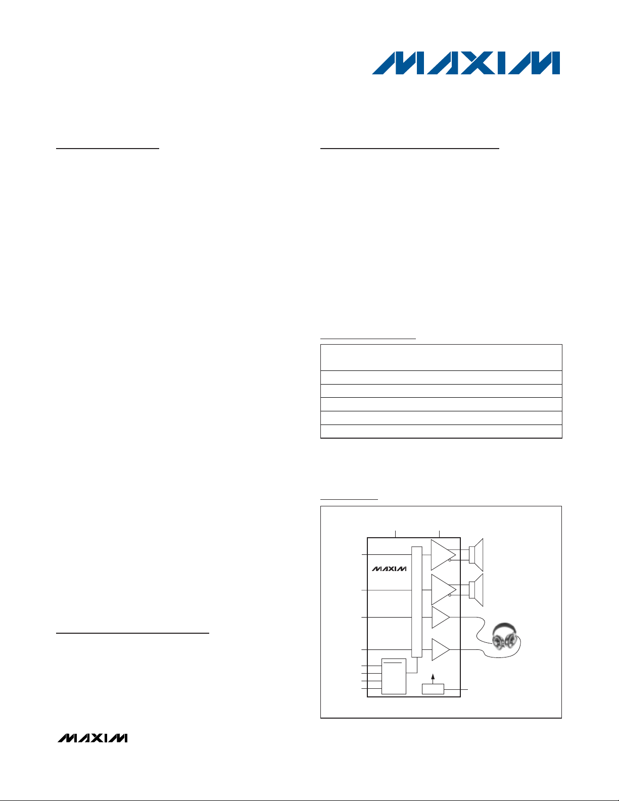
The MAX9791 combines a stereo 2W Class D power
amplifier, a stereo 180mW DirectDrive
®
headphone
amplifier, and a 120mA low-dropout (LDO) linear regulator in a single device. The MAX9792 combines a
mono 3W Class D power amplifier, a stereo 180mW
DirectDrive headphone amplifier, and a 120mA LDO
linear regulator in a single device.
The MAX9791/MAX9792 feature Maxim’s DirectDrive
headphone amplifier architecture that produces a
ground-referenced output from a single supply, eliminating the need for large DC-blocking capacitors, saving
cost, board space, and component height. High 107dB
DC PSRR and low 0.006% THD+N ensure clean, lowdistortion amplification of the audio signal.
The ground sense feature senses and corrects for the
voltage difference between the output jack ground and
device signal ground. This feature minimizes headphone amplifier crosstalk by sensing the impedance in
the ground return trace and correcting for it at the output jack. This feature also minimizes ground-loop noise
when the output socket is used as a line out connection
to other grounded equipment (for example, a PC connected to a home hi-fi system).
The MAX9791/MAX9792 feature low RF susceptibility,
allowing the amplifiers to successfully operate in close
proximity to wireless applications. The MAX9791/
MAX9792 Class D amplifiers feature Maxim’s spreadspectrum modulation and active emissions limiting circuitry. Industry-leading click-and-pop suppression
eliminates audible transients during power-up and shutdown cycles.
The MAX9791/MAX9792 wake-on-beep feature wakes
up the speaker and headphone amplifiers when a qualified beep signal is detected at the BEEP input.
For maximum flexibility, separate speaker and headphone amplifier control inputs provide independent
shutdown of the speaker and headphone amplifiers.
Additionally the LDO can be enabled independently of
the audio amplifiers.
The MAX9791/MAX9792 feature thermal-overload and
output short-circuit protection. The devices are available in 28-pin TQFN packages and are specified over
the -40°C to +85°C extended temperature range.
Applications
Notebook Computers
Tablet PCs
Portable Multimedia Players
Features
o Windows Vista® Premium Compliant
o Low EMI Filterless Class D Speaker Amplifiers
Pass EN55022B Emissions Limit with 30cm of
Speaker Cable
o 180mW DirectDrive Headphone Amplifier
o Excellent RF Immunity
o Integrated 120mA LDO
o Eliminates Headphone Ground Loop Noise
o Wake-on-Beep Function
o Click-and-Pop Suppression
o Short-Circuit and Thermal-Overload Protection
o Thermally Efficient, Space-Saving Package
28-Pin TQFN-EP (4mm x 4mm x 0.75mm)
MAX9791/MAX9792
Windows Vista-Compliant Class D Speaker
Amplifiers with DirectDrive Headphone Amplifiers
________________________________________________________________
Maxim Integrated Products
1
19-4217; Rev 1; 6/10
For pricing, delivery, and ordering information, please contact Maxim Direct at 1-888-629-4642,
or visit Maxim’s website at www.maxim-ic.com.
Ordering Information
Note: All devices are specified over the -40°C to +85°C
extended temperature range.
+
Denotes a lead(Pb)-free/RoHS-compliant package.
*
EP = Exposed pad.
DirectDrive is a registered trademark of Maxim Integrated
Products, Inc.
Windows Vista is a registered trademark of Microsoft Corp.
Simplified Block Diagrams
Simplified Block Diagrams continued at end of data sheet.
PART
MAX9791AETI+ Stereo 4.75V 28 TQFN-EP*
MAX9791BETI+ Stereo 3.3V 28 TQFN-EP*
MAX9791CETI+ Stereo 1.8V 28 TQFN-EP*
MAX9792AETI+ Mono 4.75V 28 TQFN-EP*
MAX9792CETI+ Mono 1.8V 28 TQFN-EP*
STEREO/
MONO
LDO
OUTPUT
PIN-PACKAGE
SPEAKER AND LDO
SUPPLY
2.7V TO 5.5V
MAX9791
SPKR_EN
HP_EN
LDO_EN
BEEP
HEADPHONE SUPPLY
2.7V TO 5.5V
CLASS D
AMP
CLASS D
AMP
AVDD
LDO
1.8V, 3.3V, OR 4.75V
MAX9791/MAX9792
Windows Vista-Compliant Class D Speaker
Amplifiers with DirectDrive Headphone Amplifiers
2 _______________________________________________________________________________________
ABSOLUTE MAXIMUM RATINGS
ELECTRICAL CHARACTERISTICS
(V
AVDD
= V
PVDD
= V
HPVDD
= 5V, V
GND
= V
PGND
= V
CPGND
= 0, I
LDO_OUT
= 0, C
LDO
= 2µF (C
LDO
= 4µF for 1.8V LDO option),
C1 = C2 = 1µF. R
L
= ∞, unless otherwise specified. R
IN1
= 20kΩ (A
VSPKR
= 12dB), R
IN2
= 40.2kΩ (A
VHP
= 0dB), C
IN1
= 470nF,
C
IN2=CCOM
= 1µF, TA= T
MIN
to T
MAX
, unless otherwise noted. Typical values are at TA= +25°C.) (Note 3)
Stresses beyond those listed under “Absolute Maximum Ratings” may cause permanent damage to the device. These are stress ratings only, and functional
operation of the device at these or any other conditions beyond those indicated in the operational sections of the specifications is not implied. Exposure to
absolute maximum rating conditions for extended periods may affect device reliability.
Supply Voltage
(AVDD, PVDD, HPVDD to GND)........................-0.3V to +6.0V
(AVDD to PVDD) .............................................................±0.3V
GND to PGND, CPGND ......................................................±0.3V
CPVSS, C1N to GND ............................................-6.0V to + 0.3V
HPL, HPR to CPVSS ...........................................-0.3V to lower of
(HPVDD - CPVSS + 0.3V) and +9V
HPL, HPR to HPVDD..................................+0.3V to the higher of
(CPVSS - HPVDD - 0.3V) and -9V
COM, SENSE........................................................-0.3V to + 0.3V
Any Other Pin ..........................................-0.3V to (AVDD + 0.3V)
Duration of Short Circuit between OUT_+, OUT_- and GND,
PGND, AVDD, or PVDD..........................................Continuous
Duration of Short Circuit between LDO_OUT and AVDD,
GND (Note 1) .........................................................Continuous
Duration of Short Circuit between HPR, HPL and
GND .......................................................................Continuous
Continuous Current (PVDD, OUT_+, OUT_-, PGND)............1.7A
Continuous Current (C1N, C1P, CPVSS, AVDD, HPVDD,
LDO_OUT, HPR, HPL) ..................................................850mA
Continuous Input Current (All Other Pins) ........................±20mA
Continuous Power Dissipation (T
A
= +70°C)
28-Pin Thin QFN Single-Layer Board (derate 20.8mW/°C
above +70°C)..........................................................1667mW
Junction-to-Ambient Thermal Resistance (θ
JA
)
(Note 2) .....................................................................40°C/W
Junction-to-Case Thermal Resistance (θ
JC
)
(Note 2) ....................................................................2.7°C/W
28-Pin Thin QFN Multilayer Board (derate 28.6mW/°C
above +70°C)..........................................................2286mW
Junction-to-Ambient Thermal Resistance (θ
JA
)
(Note 2) .....................................................................35°C/W
Junction-to-Case Thermal Resistance (θ
JC
)
(Note 2) ....................................................................2.7°C/W
ESD Protection, Human Body Model ...................................±2kV
Operating Temperature Range ...........................-40°C to +85°C
Junction Temperature......................................................+150°C
Storage Temperature Range .............................-65°C to +150°C
Lead Temperature (soldering, 10s) .................................+300°C
Note 1: If short is present at power-up.
Note 2: Package thermal resistances were obtained using the method described in JEDEC specification JESD51-7, using a four-layer
board. For detailed information on package thermal considerations, refer to www.maxim-ic.com/thermal-tutorial
.
GENERAL
Supply Voltage
Headphone Supply Voltage V
Undervoltage Lockout UVLO 2.65 V
Quiescent Current
Shutdown Current I
Bias Voltage V
PARAMETER SYMBOL CONDITIONS MIN TYP MAX UNITS
V
AVDD
V
PVDD
HPVDD
I
AVDD
I
PVD
I
HPVDD
SHDN
BIAS
,
Guaranteed by PSRR test (Note 4) 2.7 5.5 V
Guaranteed by PSRR test 2.7 5.5 V
MAX9791
+
+
MAX9792
SPKR_EN = 1.8V 3.3 7..3 µA
HP_INR, HP_INL, SPKR_INR, SPKR _INL 0 V
SPKR_EN HP_EN LDO_EN
1 0 1 250 400 µA
1 1 0 4.4 6
0 0 0 10.5 15
0 1 0 14.4 21
1 0 1 250 400 µA
1 1 0 4.4 6
0 0 0 10.5 18
0 1 0 14.4 24
mA
mA
MAX9791/MAX9792
Windows Vista-Compliant Class D Speaker
Amplifiers with DirectDrive Headphone Amplifiers
_______________________________________________________________________________________ 3
ELECTRICAL CHARACTERISTICS (continued)
(V
AVDD
= V
PVDD
= V
HPVDD
= 5V, V
GND
= V
PGND
= V
CPGND
= 0, I
LDO_OUT
= 0, C
LDO
= 2µF (C
LDO
= 4µF for 1.8V LDO option),
C1 = C2 = 1µF. R
L
= ∞, unless otherwise specified. R
IN1
= 20kΩ (A
VSPKR
= 12dB), R
IN2
= 40.2kΩ (A
VHP
= 0dB), C
IN1
= 470nF,
C
IN2=CCOM
= 1µF, TA= T
MIN
to T
MAX
, unless otherwise noted. Typical values are at TA= +25°C.) (Note 3)
PARAMETER S YMBOL CONDITIONS MIN TYP MAX UNITS
Shutdown to Full Operation t
ON
0.4 ms
Overtemperature Thresho ld +150 °C
SPEAKER AMPLIFIER
THD+N = 1%,
f = 1kHz,
T
= +25°C
A
(Note 5)
Output Power P
OUT
THD+N = 10%,
f = 1kHz,
T
= +25°C
A
(Note 5)
Total Harmonic Distortion Plus
Noise
THD+N
Power-Supply Rejection Ratio PSRR
RL = 8, P
R
= 4, P
L
V
AVDD
f = 217Hz, 200mV
f = 1kHz, 200mV
f = 10kHz, 200mV
Feedback Impedance R
Gain AV R
Output Offset Voltage V
Guaranteed by design 20 k
FSKR
= 20k 12 dB
IN1
OS
Measured between OUT_+ and OUT_-,
= +25°C
T
A
RL = 8,
peak voltage,
Click-and-Pop Leve l K
CP
A-weighted,
32 samples per second
(Notes 5, 6, and 7)
= 8
R
L
= 1.2W fIN = 1kH z,
Signal-to-Noise Ratio SNR
P
OUT
(Note 5)
= V
RL = 4
(MAX9791)
RL = 8
(MAX9791)
R
= 3
L
(MAX9792)
RL = 4
(MAX9791)
RL = 8
(MAX9791)
R
= 3
L
(MAX9792)
= 500mW, f = 1kHz (Note 5) 0.04
OUT
= 500mW, f = 1kHz (Note 5) 0.03
OUT
= 2.7V to 5.5V, TA = +25°C 60 80
PVDD
73
P-P
75
P-P
62
P-P
Into shutdown -52.4
Out of
shutdown
A-weighted 98
20Hz to 20kH z 94
1.7
1.2
3
2.2
1.5
3.7
±3 ±10 mV
-54
Noise VN A-weighted 38 µV
L to R, R to L, RL = 8, VIN = -20dBFS =
100mV
Crosstalk
L to R, R to L, RL = 8, VIN = -20dBFS =
100mV
HP to SPKR, R
R
LHP
, fIN = 1kHz (Note 5)
RMS
, fIN = 15kHz (Note 5)
RMS
= 8, PHP = 20mW,
LSPKR
= 32, fIN = 1kHz (Note 5)
78
70
77
W
%
dB
dBV
dB
RMS
dB
MAX9791/MAX9792
Windows Vista-Compliant Class D Speaker
Amplifiers with DirectDrive Headphone Amplifiers
4 _______________________________________________________________________________________
ELECTRICAL CHARACTERISTICS (continued)
(V
AVDD
= V
PVDD
= V
HPVDD
= 5V, V
GND
= V
PGND
= V
CPGND
= 0, I
LDO_OUT
= 0, C
LDO
= 2µF (C
LDO
= 4µF for 1.8V LDO option),
C1 = C2 = 1µF. R
L
= ∞, unless otherwise specified. R
IN1
= 20kΩ (A
VSPKR
= 12dB), R
IN2
= 40.2kΩ (A
VHP
= 0dB), C
IN1
= 470nF,
C
IN2=CCOM
= 1µF, TA= T
MIN
to T
MAX
, unless otherwise noted. Typical values are at TA= +25°C.) (Note 3)
PARAMETER S YMBOL CONDITIONS MIN TYP MAX UNITS
Class D Switching Frequenc y f
948 1158 kHz
SPK
Spread-Spectrum Bandwidth ±15 kH z
Efficiency P
= 1.5W, fIN = 1kHz, RL = 8 (Note 5) 83 %
OUT
HEADPHONE AMPLIFIER
THD+N = 1%,
Output Power P
OUT
f = 1 kH z,
T
= +25°C
A
RL = 32, fIN= 6kHz, 20kHz AES17,
V
= -3dBFS = 212mV
IN
Total Harmonic Distortion Plus
Noise
THD+N
RL = 10k, fIN = 6kHz, 20kHz AES17,
= -3dBFS = 500mV
V
IN
RL = 32, P
R
= 16, P
L
V
HPVDD
Power-Supply Rejection Ratio PSRR
f = 1 kH z, V
f = 10kHz, V
Feedback Impedance R
FHP
Gain AV R
Output Offset Voltage V
OS
38.2 40.2 42.2 k
= 40.2k 0 dB
IN2
TA = +25°C ±0.3 ±3 mV
RL = 32,
Click-and-Pop Leve l K
CP
peak voltage,
A-weighted, 32 samples
per second (Notes 6, 7)
R
= 32, P
Signal-to-Noise Ratio SNR
L
= 1kHz
f
IN
OUT
OUT
= 2.7V to 5.5V, TA = +25°C 70 107
RIPPLE
RIPPLE
OUT
RL = 16 100
= 32 180
R
L
RMS
RMS
-78
-87
= 100mW, f = 1kHz 0.006
= 75mW, f = 1 kHz 0.014
= 200mV
= 200mV
91
P-P
80
P-P
Into shutdown -81
= 40mW,
Out of
shutdown
A-weighted 102
-72.5
20Hz to 20kH z 94
Noise VN A-weighted 8 µV
Maximum Capacitive Load
Crosstalk
No sustained oscillations 100 pF
C
L
L to R, R to L, f
= 1kHz, COM
and SENSE
connected
L to R, R to L, f
= 15kHz, COM
and SENSE
connected
SPKR to HP, R
= 32, fIN = 1Hz
R
LHP
RL = 32, VIN =
IN
-20dBFS = 30mV
R
= 10k, VIN =
L
-20dBFS = 0.7mV
RL = 32, VIN =
IN
-20dBFS = 30mV
R
= 10k, VIN =
L
-20dBFS = 70.7mV
= 8, P
LSPKR
SPKR
RMS
RMS
RMS
RMS
= 1W,
82
89
64
70
80
mW
dBFS
%
dB
dBV
dB
RMS
dB
MAX9791/MAX9792
Windows Vista-Compliant Class D Speaker
Amplifiers with DirectDrive Headphone Amplifiers
_______________________________________________________________________________________ 5
ELECTRICAL CHARACTERISTICS (continued)
(V
AVDD
= V
PVDD
= V
HPVDD
= 5V, V
GND
= V
PGND
= V
CPGND
= 0, I
LDO_OUT
= 0, C
LDO
= 2µF (C
LDO
= 4µF for 1.8V LDO option),
C1 = C2 = 1µF. R
L
= ∞, unless otherwise specified. R
IN1
= 20kΩ (A
VSPKR
= 12dB), R
IN2
= 40.2kΩ (A
VHP
= 0dB), C
IN1
= 470nF,
C
IN2=CCOM
= 1µF, TA= T
MIN
to T
MAX
, unless otherwise noted. Typical values are at TA= +25°C.) (Note 3)
COM Input Range V
Common-Mode Rejection Ratio CMRR -300mV < V
PARAMETER S YMBOL CONDITIONS MIN TYP MAX UNITS
COM
Inferred from CMRR test -300 +300 mV
< +300mV 60 dB
COM
Slew Rate SR 0.38 V/µs
Charge-Pump Frequency f
OSC
530 kHz
BEEP INPUT (LDO_EN = 1)
Beep Signal Minimum
Ampl ifier Turn-On Time t
Amplifier Hold Time t
f
Four-cycle count 215 Hz
BEEP
0.4 ms
ONBEEP
HOLDBEEP
221 246 271 m s
LOW-DROPOUT LINEAR REGULATOR
LDO Ground Current I
Output Current I
Current Lim it I
Crosstalk
0.25 0.4 mA
LDO
OUT
LIM
Inferred from load regulation 120 mA
300 mA
Speaker to LDO, V
f =1kHz, I
LDO_OUT
LDO_OUT
= 4.75V,
= 10mA, speaker P
OUT
-80 dB
= 1.2W, RL = 8 (Note 6)
Output-Voltage Accuracy
Dropout Voltage V
DO
V
LDO_OUT
V
LDO_OUT
V
LDO_OUT
T
A
= 4.75V ±1.5
= 3.3V ±1.5
I
= 50mA 46
= 4.75V,
= +25°C (Note 8)
OUT
I
= 120mA 106
OUT
Startup Time 30 µs
V
Line Regulation
Load Regulation
Ripple Rejection
Output-Voltage Noi se
= 5V to 5.5V, V
AVDD
I
LDO_OUT
V
AVDD
I
LDO_OUT
V
AVDD
I
LDO_OUT
V
LDO_OUT
= 1mA, C
= 4.5V to 5.5V, V
= 1mA, C
= 3V to 5.5V, V
= 1mA, C
= 4.75V, 1mA < I
120mA
V
V
I
RIPPLE
LDO_OUT
LDO_OUT
= 200mV
= 4.75V
= 10mA
20Hz to 20kHz, C
I
LDO_OUT
= 120mA
LDO_OUT
LDO
LDO
LDO_OUT
LDO
,
P-P
LDO_OUT
= 2µF
LDO_OUT
= 2µF
= 4µF
LDO_OUT
= 4.75V,
= 3.3V,
= 1.8V,
<
-4.8 1.5 +4.8
-4 0.2 +4
-6.4 2.5 +6.4
0.22 mV/mA
f = 1kHz 56
f = 10kHz 40
= 2 x 1µF,
130 µV
DIGITAL INPUTS (SPKR_EN, HP_EN, LDO_EN, BEEP)
Input-Voltage High V
Input-Voltage Low V
INH
INL
1.4 V
0.4 V
Input Bias Current -1 +1 µA
%
mV
mV/V
dB
RMS
Typical Operating Characteristics
(V
AVDD
= V
PVDD
= V
HPVDD
= 5V, V
GND
= V
PGND
= V
CPGND
= 0, I
LDO_OUT
= 0, C
LDO
= 2 x 1µF, C1 = C2 = 1µF. RL= ∞, unless oth-
erwise specified. R
IN1
= 20kΩ (A
VSPKR
= 12dB), R
IN2
= 40.2kΩ (A
VHP
= 0dB), C
IN1
= 470nF, C
IN2
= C
COM
= 1µF, measurement BW
= 20kHz AES17, T
A
= +25°C, unless otherwise noted. Speaker mode: SPKR_EN = 0, HP_EN = 0. Headphone mode: SPKR_EN = 1,
HP_EN = 1.)
MAX9791/MAX9792
Windows Vista-Compliant Class D Speaker
Amplifiers with DirectDrive Headphone Amplifiers
6 _______________________________________________________________________________________
Note 3: All devices are 100% production tested at room temperature. All temperature limits are guaranteed by design.
Note 4: AVDD and PVDD must be tied together. If LDO is enabled, set AVDD and PVDD as specified in the Line Regulation row of
the
Electrical Characteristics
table.
Note 5: Testing performed with a resistive load in series with an inductor to simulate an actual speaker load. For R
L
= 3Ω, L = 22µH.
For R
L
= 4Ω, L = 33µH. For RL= 8Ω, L = 68µH.
Note 6: Specified at T
A
= +25°C with an 8Ω + 68µH load connected across BTL output for speaker amplifier. Specified at TA= +25°C
with a 32Ω resistive load connected between HPR, HPL and GND for headphone amplifier. Speaker and headphone mode
transitions are controlled by SPKR_EN and HP_EN inputs, respectively.
Note 7: Amplifier Inputs AC-coupled to GND.
Note 8: Guaranteed by ATE characterization; limits are not production tested.
TOTAL HARMONIC DISTORTION + NOISE
vs. FREQUENCY (MAX9792 SPEAKER MODE)
MAX9791 toc01
FREQUENCY (kHz)
THD+N (dBFS)
0.1 1 10
-90
-80
-50
-40
-30
-70
-60
-20
-10
0
-100
0.01 100
RL = 3
Ω
V
IN
= -3dBFS
FS = 707mV
RMS
FS = 1V
RMS
TOTAL HARMONIC DISTORTION + NOISE
vs. FREQUENCY (MAX9791 SPEAKER MODE)
MAX9791 toc02
FREQUENCY (kHz)
THD+N (dBFS)
0.1 1 10
-90
-80
-50
-40
-30
-70
-60
-20
-10
0
-100
0.01 100
RL = 4
Ω
V
IN
= -3dBFS
FS = 707mV
RMS
FS = 1V
RMS
TOTAL HARMONIC DISTORTION + NOISE
vs. FREQUENCY (MAX9791 SPEAKER MODE)
MAX9791 toc03
FREQUENCY (kHz)
THD+N (dBFS)
0.1 1 10
-90
-80
-50
-40
-30
-70
-60
-20
-10
0
-100
0.01 100
RL = 8
Ω
V
IN
= -3dBFS
FS = 707mV
RMS
FS = 1V
RMS
TOTAL HARMONIC DISTORTION + NOISE
vs. OUTPUT POWER (MAX9792 SPEAKER MODE)
MAX9791 toc04
OUTPUT POWER (W)
THD+N (%)
1.0 2.0 3.0
0.01
0.1
1
10
100
0.001
0 4.00.5 1.5 2.5 3.5
RL = 3
Ω
f = 6kHz
f = 1kHz
f = 100Hz
TOTAL HARMONIC DISTORTION + NOISE
vs. OUTPUT POWER (MAX9791 SPEAKER MODE)
MAX9791 toc05
OUTPUT POWER (W)
THD+N (%)
2.01.51.0
0.01
0.1
1
10
100
0.001
0 3.02.50.5
RL = 4
Ω
f = 6kHz
f = 1kHz
f = 100Hz
TOTAL HARMONIC DISTORTION + NOISE
vs. OUTPUT POWER (MAX9791 SPEAKER MODE)
MAX9791 toc06
OUTPUT POWER (W)
THD+N (%)
0.5 1.0
0.01
0.1
1
10
100
0.001
02.01.5
RL = 8
Ω
f = 6kHz
f = 1kHz
f = 100Hz
ELECTRICAL CHARACTERISTICS (continued)
(V
AVDD
= V
PVDD
= V
HPVDD
= 5V, V
GND
= V
PGND
= V
CPGND
= 0, I
LDO_OUT
= 0, C
LDO
= 2µF (C
LDO
= 4µF for 1.8V LDO option),
C1 = C2 = 1µF. R
L
= ∞, unless otherwise specified. R
IN1
= 20kΩ (A
VSPKR
= 12dB), R
IN2
= 40.2kΩ (A
VHP
= 0dB), C
IN1
= 470nF,
C
IN2=CCOM
= 1µF, TA= T
MIN
to T
MAX
, unless otherwise noted. Typical values are at TA= +25°C.) (Note 3)
SPEAKER
Typical Operating Characteristics (continued)
(V
AVDD
= V
PVDD
= V
HPVDD
= 5V, V
GND
= V
PGND
= V
CPGND
= 0, I
LDO_OUT
= 0, C
LDO
= 2 x 1µF, C1 = C2 = 1µF. RL= ∞, unless oth-
erwise specified. R
IN1
= 20kΩ (A
VSPKR
= 12dB), R
IN2
= 40.2kΩ (A
VHP
= 0dB), C
IN1
= 470nF, C
IN2
= C
COM
= 1µF, measurement BW
= 20kHz AES17, T
A
= +25°C, unless otherwise noted. Speaker mode: SPKR_EN = 0, HP_EN = 0. Headphone mode: SPKR_EN = 1,
HP_EN = 1.)
MAX9791/MAX9792
Windows Vista-Compliant Class D Speaker
Amplifiers with DirectDrive Headphone Amplifiers
_______________________________________________________________________________________
7
SPEAKER
OUTPUT POWER vs. LOAD RESISTANCE
(MAX9791 SPEAKER MODE)
3.0
2.5
2.0
1.5
1.0
OUTPUT POWER (W)
0.5
0
1 100
EFFICIENCY vs. OUTPUT POWER
(MAX9792 SPEAKER MODE)
90
RL = 8
80
70
60
50
40
EFFICIENCY (%)
30
20
10
0
01.5
OUTPUT POWER (W)
LOAD RESISTANCE (Ω)
Ω
OUTPUT POWER (W)
OUTPUT POWER vs. LOAD RESISTANCE
(MAX9792 SPEAKER MODE)
5.0
4.5
4.0
3.5
3.0
2.5
2.0
1.5
1.0
0.5
0
1 100
LOAD RESISTANCE (Ω)
f = 1kHz
THD+N = 10%
THD+N = 1%
10
RL = 3
Ω
V
= V
AVDD
= 3.7V
1.20.90.60.3
f
PVDD
IN
= 1kHz
f = 1kHz
THD+N = 10%
THD+N = 1%
10
MAX9791 toc08
MAX9791 toc09a
1.50
1.25
1.00
0.75
0.50
OUTPUT POWER (W)
0.25
100
EFFICIENCY (%)
MAX9791 toc07
OUTPUT POWER vs. LOAD RESISTANCE
(MAX9791 SPEAKER MODE)
V
PVDD
THD+N = 1%
0
1 100
EFFICIENCY vs. OUTPUT POWER
(MAX9791 SPEAKER MODE)
90
80
70
60
50
40
30
20
10
0
01.81.20.3
10
LOAD RESISTANCE (Ω)
OUTPUT POWER (W)
OUTPUT POWER vs. LOAD RESISTANCE
(MAX9792 SPEAKER MODE)
2.5
2.0
1.5
1.0
OUTPUT POWER (W)
0.5
0
1100
LOAD RESISTANCE (Ω)
THD+N = 1%
10
V
= V
PVDD
AVDD
THD+N = 10%
= 3.7V
MAX9791 toc07a
EFFICIENCY vs. OUTPUT POWER
(MAX9792 SPEAKER MODE)
MAX9791 toc08a
110
100
90
80
70
60
50
EFFICIENCY (%)
40
30
20
10
0
04.00.5 1.5 2.5 3.5
1.0 2.0 3.0
OUTPUT POWER (W)
RL = 8
RL = 3
fIN = 1kHz
Ω
= V
AVDD
THD+N = 10%
= 3.7V
EFFICIENCY vs. OUTPUT POWER
(MAX9791 SPEAKER MODE)
90
RL = 8
Ω
RL = 4
fIN = 1kHz
Ω
1.50.90.6
MAX9791 toc10
80
70
60
50
40
EFFICIENCY (%)
30
20
10
RL = 8
Ω
RL = 4
Ω
V
= V
PVDD
AVDD
= 1kHz
f
0
01.0
IN
OUTPUT POWER (W)
MAX9791 toc09
Ω
MAX9791 toc10a
= 3.7V
0.80.60.40.2
MAX9791/MAX9792
Windows Vista-Compliant Class D Speaker
Amplifiers with DirectDrive Headphone Amplifiers
8 _______________________________________________________________________________________
Typical Operating Characteristics (continued)
(V
AVDD
= V
PVDD
= V
HPVDD
= 5V, V
GND
= V
PGND
= V
CPGND
= 0, I
LDO_OUT
= 0, C
LDO
= 2 x 1µF, C1 = C2 = 1µF. RL= ∞, unless oth-
erwise specified. R
IN1
= 20kΩ (A
VSPKR
= 12dB), R
IN2
= 40.2kΩ (A
VHP
= 0dB), C
IN1
= 470nF, C
IN2
= C
COM
= 1µF, measurement BW
= 20kHz AES17, T
A
= +25°C, unless otherwise noted. Speaker mode: SPKR_EN = 0, HP_EN = 0. Headphone mode: SPKR_EN = 1,
HP_EN = 1.)
SPEAKER
3.0
2.5
2.0
1.5
1.0
OUTPUT POWER (W)
0.5
0
2.5 5.5
OUTPUT POWER vs. SUPPLY VOLTAGE
(MAX9791 SPEAKER MODE)
f = 1kHz
= 4
R
Ω
LOAD
THD+N = 10%
THD+N = 1%
5.04.54.03.53.0
SUPPLY VOLTAGE (V)
MAX9791 toc10b
OUTPUT POWER (W)
OUTPUT POWER vs. SUPPLY VOLTAGE
2.0
1.5
1.0
0.5
(MAX9791 SPEAKER MODE)
f = 1kHz
= 8
R
Ω
LOAD
THD+N = 10%
THD+N = 1%
0
2.5 5.5
SUPPLY VOLTAGE (V)
OUTPUT POWER vs. SUPPLY VOLTAGE
(MAX9792 SPEAKER MODE)
2.5
f = 1kHz
= 8
R
Ω
MAX9791 toc10c
5.04.54.03.53.0
LOAD
2.0
1.5
1.0
OUTPUT POWER (W)
0.5
0
2.5 5.5
THD+N = 10%
SUPPLY VOLTAGE (V)
THD+N = 1%
MAX9791 toc10d
5.04.54.03.53.0
OUTPUT POWER vs. SUPPLY VOLTAGE
(MAX9792 SPEAKER MODE)
5.0
f = 1kHz
4.5
4.0
3.5
3.0
2.5
2.0
OUTPUT POWER (W)
1.5
1.0
0.5
= 3
R
Ω
LOAD
THD+N = 10%
THD+N = 1%
0
2.5 5.5
SUPPLY VOLTAGE
POWER-SUPPLY REJECTION RATIO
vs. FREQUENCY (SPEAKER MODE)
0
V
= 200mV
RIPPLE
-10
MAX9791 toc10e
5.04.54.03.53.0
RL = 8
-20
-30
-40
-50
PSRR (dB)
-60
-70
-80
-90
-100
0.01 100
P-P
Ω
LEFT
0.1 10
1
FREQUENCY (kHz)
RIGHT
MAX9791 toc11
-10
-20
-30
-40
-50
-60
-70
CROSSTALK (dB)
-80
-90
-100
-110
CROSSTALK vs. FREQUENCY
(SPEAKER MODE)
0
FS = 1V
RMS
VIN = -20dBFS
= 8
R
Ω
L
RIGHT TO LEFT
LEFT TO RIGHT
0.01 100
0.1 10
1
FREQUENCY (kHz)
MAX9791 toc12
Typical Operating Characteristics (continued)
(V
AVDD
= V
PVDD
= V
HPVDD
= 5V, V
GND
= V
PGND
= V
CPGND
= 0, I
LDO_OUT
= 0, C
LDO
= 2 x 1µF, C1 = C2 = 1µF. RL= ∞, unless oth-
erwise specified. R
IN1
= 20kΩ (A
VSPKR
= 12dB), R
IN2
= 40.2kΩ (A
VHP
= 0dB), C
IN1
= 470nF, C
IN2
= C
COM
= 1µF, measurement BW
= 20kHz AES17, T
A
= +25°C, unless otherwise noted. Speaker mode: SPKR_EN = 0, HP_EN = 0. Headphone mode: SPKR_EN = 1,
HP_EN = 1.)
MAX9791/MAX9792
Windows Vista-Compliant Class D Speaker
Amplifiers with DirectDrive Headphone Amplifiers
_______________________________________________________________________________________
9
µ
µ
SPEAKER
0
-10
-20
-30
-40
-50
-60
-70
-80
OUTPUT AMPLITUDE (dBV)
-90
-100
-110
-120
0 100
RBW = 1kHz
INPUT AC GROUNDED
SPEAKER STARTUP WAVEFORM
s/div
200
MAX9791 toc13
WIDEBAND OUTPUT SPECTRUM
(SPEAKER MODE)
101
FREQUENCY (MHz)
SPKR_EN
2V/div
SPEAKER OUT
MAX9791 toc15
SPEAKER SHUTDOWN WAVEFORM
s/div
200
MAX9791 toc14
OUTPUT FREQUENCY SPECTRUM
(SPEAKER MODE)
0
V
= -60dBV
OUT
f = 1kHz
-20
= 8
R
Ω
L
UNWEIGHTED
-40
-60
-80
-100
OUTPUT MAGNITUDE (dBV)
-120
-140
120515
10
FREQUENCY (kHz)
SPKR_EN
2V/div
SPEAKER OUT
MAX9791 toc16
MAX9791/MAX9792
Windows Vista-Compliant Class D Speaker
Amplifiers with DirectDrive Headphone Amplifiers
10 ______________________________________________________________________________________
Typical Operating Characteristics (continued)
(V
AVDD
= V
PVDD
= V
HPVDD
= 5V, V
GND
= V
PGND
= V
CPGND
= 0, I
LDO_OUT
= 0, C
LDO
= 2 x 1µF, C1 = C2 = 1µF. RL= ∞, unless oth-
erwise specified. R
IN1
= 20kΩ (A
VSPKR
= 12dB), R
IN2
= 40.2kΩ (A
VHP
= 0dB), C
IN1
= 470nF, C
IN2
= C
COM
= 1µF, measurement BW
= 20kHz AES17, T
A
= +25°C, unless otherwise noted. Speaker mode: SPKR_EN = 0, HP_EN = 0. Headphone mode: SPKR_EN = 1,
HP_EN = 1.)
HEADPHONE
TOTAL HARMONIC DISTORTION + NOISE
-50
-60
vs. FREQUENCY (HEADPHONE MODE)
RL = 16
Ω
= -3dBFS
V
IN
MAX9791 toc17
TOTAL HARMONIC DISTORTION + NOISE
vs. FREQUENCY (HEADPHONE MODE)
-50
V
= 3V
HPVDD
= 16
R
Ω
L
= -3dBFS
V
IN
-60
TOTAL HARMONIC DISTORTION + NOISE
vs. FREQUENCY (HEADPHONE MODE)
-50
RL = 32
Ω
= -3dBFS
V
MAX9791 toc18
IN
-60
MAX9791 toc19
-70
-80
THD+N (dBFS)
-90
-100
0.01 100
FS = 300mV
RMS
FS = 1V
RMS
0.1 10
1
FREQUENCY (kHz)
THD+N (dBFS)
TOTAL HARMONIC DISTORTION + NOISE
vs. FREQUENCY (HEADPHONE MODE)
-50
V
= 3V
HPVDD
= 32
R
Ω
L
= -3dBFS
V
IN
-60
-70
FS = 300mV
RMS
-80
THD+N (dBFS)
-90
-100
0.01 100
FS = 1V
RMS
0.1 10
1
FREQUENCY (kHz)
MAX9791 toc20
THD+N (%)
TOTAL HARMONIC DISTORTION + NOISE
vs. OUTPUT POWER (HEADPHONE MODE)
100
V
= 3V
HPVDD
= 16
R
Ω
L
10
MAX9791 toc23
-70
-80
-90
-100
0.01 100
FS = 300mV
FS = 1V
0.1 10
FREQUENCY (kHz)
RMS
RMS
1
TOTAL HARMONIC DISTORTION + NOISE
vs. OUTPUT POWER (HEADPHONE MODE)
100
RL = 16
Ω
10
1
f = 6kHz
0.1
0.01
0.001
f = 1kHz
f = 100Hz
0 200
OUTPUT POWER (mW)
12040 80
TOTAL HARMONIC DISTORTION + NOISE
vs. OUTPUT POWER (HEADPHONE MODE)
100
V
= 3V
HPVDD
= 32
R
Ω
L
10
160
MAX9791 toc21
MAX9791 toc24A
-70
FS = 300mV
-80
THD+N (dBFS)
-90
-100
0.01 100
RMS
FS = 1V
RMS
0.1 10
1
FREQUENCY (kHz)
TOTAL HARMONIC DISTORTION + NOISE
vs. OUTPUT POWER (HEADPHONE MODE)
100
RL = 32
Ω
10
1
THD+N (%)
0.1
f = 100Hz
0.01
0.001
050 250
f = 1kHz
100
150
OUTPUT POWER (mW)
f = 6kHz
200
OUTPUT POWER vs. LOAD RESISTANCE
(HEADPHONE MODE)
250
200
f = 1kHz
THD+N = 10%
MAX9791 toc22
MAX9791 toc25
1
f = 100Hz
THD+N (%)
0.1
f = 1kHz
0.01
0.001
05040 90
10
OUTPUT POWER (mW)
1
THD+N (%)
f = 6kHz
80
603020
70
0.1
f = 100Hz
0.01
0.001
05040 70
10
f = 1kHz
f = 6kHz
603020
OUTPUT POWER (mW)
150
100
OUTPUT POWER (mW)
50
0
1100
LOAD RESISTANCE (Ω)
THD+N = 1%
10
MAX9791/MAX9792
Windows Vista-Compliant Class D Speaker
Amplifiers with DirectDrive Headphone Amplifiers
______________________________________________________________________________________
11
Typical Operating Characteristics (continued)
(V
AVDD
= V
PVDD
= V
HPVDD
= 5V, V
GND
= V
PGND
= V
CPGND
= 0, I
LDO_OUT
= 0, C
LDO
= 2 x 1µF, C1 = C2 = 1µF. RL= ∞, unless oth-
erwise specified. R
IN1
= 20kΩ (A
VSPKR
= 12dB), R
IN2
= 40.2kΩ (A
VHP
= 0dB), C
IN1
= 470nF, C
IN2
= C
COM
= 1µF, measurement BW
= 20kHz AES17, T
A
= +25°C, unless otherwise noted. Speaker mode: SPKR_EN = 0, HP_EN = 0. Headphone mode: SPKR_EN = 1,
HP_EN = 1.)
HEADPHONE
OUTPUT POWER vs. LOAD RESISTANCE
(HEADPHONE MODE)
90
80
70
60
50
40
30
OUTPUT POWER (mW)
20
10
0
10 1000
100
LOAD RESISTANCE (Ω)
HEADPHONE OUTPUT POWER
vs. HPVDD
250
THD+N = 1%
f = 1kHz
200
150
100
50
HEADPHONE OUTPUT POWER (mW)
0
2.5 5.5
RL = 32
HPVDD (V)
V
HPVDD
f = 1kHz
THD+N = 10%
THD+N = 1%
Ω
RL = 16
= 3V
Ω
5.04.54.03.53.0
400
350
MAX9791 toc26
300
250
200
150
100
50
POWER DISSIPATION PER CHANNEL (mW)
0
0
-10
-20
MAX9791 toc29
-30
-40
-50
-60
PSRR (dB)
-70
-80
-90
-100
-110
-120
POWER DISSIPATION vs. OUTPUT POWER
0 20025 75 125 175
0.01 100
(HEADPHONE MODE)
RL = 16
Ω
RL = 32
Ω
50 100 150
PER CHANNEL OUTPUT POWER (mW)
POWER-SUPPLY REJECTION RATIO
vs. FREQUENCY (HEADPHONE MODE)
V
= 200mV
RIPPLE
RL = 32
P-P
Ω
RIGHT
0.1 1 10
FREQUENCY (kHz)
LEFT
POWER DISSIPATION vs. OUTPUT POWER
(HEADPHONE MODE)
300
V
= 3V
HPVDD
250
MAX9791 toc27
200
150
100
50
POWER DISSIPATION PER CHANNEL (mW)
0
20
01008040 60
PER CHANNEL OUTPUT POWER (mW)
CROSSTALK vs. FREQUENCY
(HEADPHONE MODE)
-20
RIGHT TO LEFT
-30
MAX9791 toc30
COM AND SENSE
DISABLED
-40
-50
-60
-70
CROSSTALK (dB)
-80
-90
-100
0.01 100
RIGHT TO LEFT
COM AND SENSE
DISABLED
RIGHT TO LEFT
COM AND SENSE
0.1 1 10
RL = 16
Ω
RL = 32
LEFT TO RIGHT
COM AND SENSE
FREQUENCY (kHz)
Ω
RL = 32
FS = 300mV
VIN = -20dBFS
MAX9791 toc28
Ω
RMS
MAX9791 toc31

MAX9791/MAX9792
Windows Vista-Compliant Class D Speaker
Amplifiers with DirectDrive Headphone Amplifiers
12 ______________________________________________________________________________________
HEADPHONE
Typical Operating Characteristics (continued)
(V
AVDD
= V
PVDD
= V
HPVDD
= 5V, V
GND
= V
PGND
= V
CPGND
= 0, I
LDO_OUT
= 0, C
LDO
= 2 x 1µF, C1 = C2 = 1µF. RL= ∞, unless oth-
erwise specified. R
IN1
= 20kΩ (A
VSPKR
= 12dB), R
IN2
= 40.2kΩ (A
VHP
= 0dB), C
IN1
= 470nF, C
IN2
= C
COM
= 1µF, measurement BW
= 20kHz AES17, T
A
= +25°C, unless otherwise noted. Speaker mode: SPKR_EN = 0, HP_EN = 0. Headphone mode: SPKR_EN = 1,
HP_EN = 1.)
OUTPUT FREQUENCY SPECTRUM
(HEADPHONE MODE)
RIGHT AND LEFT
0
FS = 707mV
VIN = -60dBFS
-20
= 32
R
Ω
L
-40
-60
-80
-100
OUTPUT FREQUENCY SPECTRUM (dB)
-120
-140
020
51015
RMS
FREQUENCY (kHz)
MAX9791 toc32
STARTUP WAVEFORM
200µs/div
MAX9791 toc33
HP_EN
2V/div
HP_
500mV/div
SHUTDOWN WAVEFORM
200µs/div
MAX9791 toc34
HP_EN
2V/div
HP_
500mV/div
HEADPHONE RF IMMUNITY
vs. FREQUENCY
RL = 32Ω
-10
-30
-50
-70
AMPLITUDE (dBV)
-90
-110
-130
500 15001000 2000 2500 3000
LEFT
RIGHT
FREQUENCY (MHz)
MAX9791 toc35

MAX9791/MAX9792
Windows Vista-Compliant Class D Speaker
Amplifiers with DirectDrive Headphone Amplifiers
______________________________________________________________________________________
13
Typical Operating Characteristics (continued)
(V
AVDD
= V
PVDD
= V
HPVDD
= 5V, V
GND
= V
PGND
= V
CPGND
= 0, I
LDO_OUT
= 0, C
LDO
= 2 x 1µF, C1 = C2 = 1µF. RL= ∞, unless oth-
erwise specified. R
IN1
= 20kΩ (A
VSPKR
= 12dB), R
IN2
= 40.2kΩ (A
VHP
= 0dB), C
IN1
= 470nF, C
IN2
= C
COM
= 1µF, measurement BW
= 20kHz AES17, T
A
= +25°C, unless otherwise noted. Speaker mode: SPKR_EN = 0, HP_EN = 0. Headphone mode: SPKR_EN = 1,
HP_EN = 1.)
LINE OUT
TOTAL HARMONIC DISTORTION + NOISE
vs. FREQUENCY (HEADPHONE MODE)
0
RL = 10k
-10
-20
-30
-40
-50
-60
THD+N (dBFS)
-70
-80
-90
-100
-110
0.01 100
Ω
= -3dBFS
V
IN
FS = 707mV
0.1 1 10
FREQUENCY (kHz)
RMS
TOTAL HARMONIC DISTORTION + NOISE
vs. OUTPUT POWER (HEADPHONE MODE)
100
V
= 3V
HPVDD
= 10k
R
Ω
L
10
1
0.1
THD+N (%)
0.01
0.001
0.0001
f = 6kHz
03.02.50.5
f = 100Hz
f = 1kHz
OUTPUT POWER (mW)
FS = 1V
2.01.51.0
RMS
MAX9791 toc36
MAX9791 toc39
0
-10
-20
-30
-40
-50
-60
THD+N (dBFS)
-70
-80
-90
-100
-110
-20
-30
-40
-50
-60
-70
-80
CROSSTALK (dB)
-90
-100
-110
-120
TOTAL HARMONIC DISTORTION + NOISE
vs. FREQUENCY (HEADPHONE MODE)
V
= 3V
HPVDD
= 10k
R
Ω
L
= -3dBFS
V
IN
FS = 707mV
0.01 100
0.1 1 10
FREQUENCY (kHz)
CROSSTALK vs. FREQUENCY
(HEADPHONE MODE)
RIGHT TO LEFT
COM AND SENSE
0.01 100
0.1 1 10
FREQUENCY (kHz)
RMS
LEFT TO RIGHT
COM AND SENSE
FS = 1V
RMS
RL = 10k
FS = 707mV
VIN = -20dBFS
Ω
RMS
TOTAL HARMONIC DISTORTION + NOISE
vs. OUTPUT POWER (HEADPHONE MODE)
100
RL = 10k
Ω
10
MAX9791 toc37
1
0.1
THD+N (%)
0.01
0.001
0.0001
1.0 2.0 3.0
04.00.5 1.5 2.5 3.5
OUTPUT FREQUENCY SPECTRUM
(HEADPHONE MODE)
RIGHT AND LEFT
0
= 10k
R
Ω
MAX9791 toc40
L
FS = 300mV
-20
VIN = -60dBFS
-40
-60
-80
-100
OUTPUT FREQUENCY SPECTRUM (dB)
-120
-140
020
51015
f = 6kHz
f = 1kHz
OUTPUT POWER (mW)
RMS
FREQUENCY (kHz)
f = 100Hz
MAX9791 toc38
MAX9791 toc41

MAX9791/MAX9792
Windows Vista-Compliant Class D Speaker
Amplifiers with DirectDrive Headphone Amplifiers
14 ______________________________________________________________________________________
Typical Operating Characteristics (continued)
(V
AVDD
= V
PVDD
= V
HPVDD
= 5V, V
GND
= V
PGND
= V
CPGND
= 0, I
LDO_OUT
= 0, C
LDO
= 2 x 1µF, C1 = C2 = 1µF. RL= ∞, unless oth-
erwise specified. R
IN1
= 20kΩ (A
VSPKR
= 12dB), R
IN2
= 40.2kΩ (A
VHP
= 0dB), C
IN1
= 470nF, C
IN2
= C
COM
= 1µF, measurement BW
= 20kHz AES17, T
A
= +25°C, unless otherwise noted. Speaker mode: SPKR_EN = 0, HP_EN = 0. Headphone mode: SPKR_EN = 1,
HP_EN = 1.)
GENERAL
SUPPLY CURRENT vs. SUPPLY VOLTAGE
20
15
10
5
SUPPLY CURRENT (mA)
0
-5
4.50 5.505.25
LDO_EN = 1, V
SPKR_EN = 0
HP_EN = 1
SPKR_EN = 1
HP_EN = 0
4.75 5.00
SHUTDOWN CURRENT vs. SUPPLY VOLTAGE
8
SPKR_EN = 1
7
HP_EN = 0
LDO_EN = 0
6
5
4
3
SHUTDOWN CURRENT (µA)
2
1
0
2.5 5.5
SUPPLY VOLTAGE (V)
= 3.3V OR 4.75V
LDO
SPKR_EN = 0
HP_EN = 0
SPKR_EN = 1
HP_EN = 1
SUPPLY VOLTAGE (V)
20
MAX9791 toc42
15
10
5
SUPPLY CURRENT (mA)
0
-5
SUPPLY CURRENT vs. SUPPLY VOLTAGE
LDO_EN = 1
= 1.8V
V
LDO_OUT
2.5 5.5
SUPPLY VOLTAGE (V)
SPKR_EN = 1
SPKR_EN = 1
SPKR_EN = 0
SPKR_EN = 0
5.04.54.03.53.0
MAX9791 toc42a
MAX9791 toc43
5.04.53.0 3.5 4.0

MAX9791/MAX9792
Windows Vista-Compliant Class D Speaker
Amplifiers with DirectDrive Headphone Amplifiers
______________________________________________________________________________________
15
Typical Operating Characteristics (continued)
(V
AVDD
= V
PVDD
= V
HPVDD
= 5V, V
GND
= V
PGND
= V
CPGND
= 0, I
LDO_OUT
= 0, C
LDO
= 2 x 1µF, C1 = C2 = 1µF. RL= ∞, unless oth-
erwise specified. R
IN1
= 20kΩ (A
VSPKR
= 12dB), R
IN2
= 40.2kΩ (A
VHP
= 0dB), C
IN1
= 470nF, C
IN2
= C
COM
= 1µF, measurement BW
= 20kHz AES17, T
A
= +25°C, unless otherwise noted. Speaker mode: SPKR_EN = 0, HP_EN = 0. Headphone mode: SPKR_EN = 1,
HP_EN = 1.)
LDO
LDO OUTPUT ACCURACY
2.0
1.5
1.0
0.5
0
-0.5
-1.0
LDO OUTPUT ACCURACY (%)
-1.5
-2.0
0 15025 10050
LDO DROPOUT VOLTAGE vs. LOAD
300
LDO_OUT = 4.75V
250
200
150
100
LDO DROPOUT VOLTAGE (mV)
50
0
0 100 15050 200 250 300
vs. LOAD CURRENT
LOAD CURRENT (mA)
I
LOAD
(mA)
LDO OUTPUT ACCURACY
vs. AMPLIFIER OUTPUT POWER
0.10
0.09
MAX9791 toc44
0.08
0.07
0.06
0.05
0.04
0.03
LDO OUTPUT ACCURACY (%)
0.02
0.01
12575
0
300
0 15001200600 900
AMPLIFIER OUTPUT POWER (mW)
1.0
MAX9791 toc45
0.5
0
-0.5
LDO OUTPUT ACCURACY (%)
-1.0
LDO POWER-SUPPLY REJECTION RATIO
vs. FREQUENCY
MAX9791 toc47
40
V
= 200mV
RIPPLE
I
LOAD
20
0
-20
V
PSRR (dB)
-40
LDO_OUT
-60
-80
-100
0.01 100
= 10mA
= 4.75V
P-P
V
LDO_OUT
V
LDO_OUT
FREQUENCY (kHz)
= 3.3V
= 1.8V
1010.1
MAX9791 toc48
200
175
150
125
100
LDO OUTPUT NOISE (µV)
75
50
LDO OUTPUT ACCURACY
vs. TEMPERATURE
V
V
LDO_OUT
LDO_OUT
= 4.75V
V
= 3.3V
LDO_OUT
-40 85
TEMPERATURE (°C)
LDO OUTPUT NOISE
C
LOAD
I
LOAD
0.01 100
FREQUENCY (kHz)
1010.1
= 1.8V
603510-15
= 2 x 1µF
= 120mA
MAX9791 toc46
MAX9791 toc49

MAX9791/MAX9792
Windows Vista-Compliant Class D Speaker
Amplifiers with DirectDrive Headphone Amplifiers
16 ______________________________________________________________________________________
Typical Operating Characteristics (continued)
(V
AVDD
= V
PVDD
= V
HPVDD
= 5V, V
GND
= V
PGND
= V
CPGND
= 0, I
LDO_OUT
= 0, C
LDO
= 2 x 1µF, C1 = C2 = 1µF. RL= ∞, unless oth-
erwise specified. R
IN1
= 20kΩ (A
VSPKR
= 12dB), R
IN2
= 40.2kΩ (A
VHP
= 0dB), C
IN1
= 470nF, C
IN2
= C
COM
= 1µF, measurement BW
= 20kHz AES17, T
A
= +25°C, unless otherwise noted. Speaker mode: SPKR_EN = 0, HP_EN = 0. Headphone mode: SPKR_EN = 1,
HP_EN = 1.)
LDO
LINE-TRANSIENT RESPONSE
MAX9791 toc50
1.00ms/div
SHUTDOWN RESPONSE
200µs/div
MAX9791 toc52
CH1 LOW
4.560V
CH1 HIGH
5.500V
CH2 LOW
800.0µV
CH2 HIGH
1.000mV
LDO_EN
2V/div
V
LDO_EN
2V/div
LOAD-TRANSIENT RESPONSE
100ms/div
CROSSTALK vs. FREQUENCY
SPEAKER TO LDO
0
BOTH SPEAKERS WITH SIGNAL
-10
-20
-30
-40
-50
-60
-70
-80
CROSSTALK (dB)
-90
-100
-110
-120
-130
= 1.2W
P
SPKR
= 8W
R
LSPKR
= 10mA
I
LDO
LEFT CHANNEL TO LDO
RIGHT CHANNEL TO LDO
0.01 100
FREQUENCY (kHz)
1010.1
MAX9791 toc51
I
LDO_OUT
50mA/div
AC-COUPLED
V
LDO_OUT
10mV/div
MAX9791 toc53
MAX9791/MAX9792
Windows Vista-Compliant Class D Speaker
Amplifiers with DirectDrive Headphone Amplifiers
______________________________________________________________________________________ 17
MAX9791 Pin Description
PIN NAME FUNCTION
1 SPKR_INL Left-Channe l Speaker Amplif ier Input
2 HP_INR R ight-Channel Headphone Ampl ifier Input
3 HP_INL Left-Channe l Headphone Amplifier Input
4 COM Common-Mode Voltage Sense Input
5 GND Signal Ground. Star connect to PGND.
6 LDO_OUT
7 AVDD Positive Power-Supply and LDO Input. Bypass with a 0.1µF and two 1µF capacitors to GND.
8 LDO_EN LDO Enable. Connect LDO_EN to AVDD to enable the LDO.
9 HPR Right-Channel Headphone Amplifier Output
10 HPL Left-Channe l Headphone Amplifier Output
11 SENSE Headphone Ground Sense
12 CPVSS Headphone Ampl if ier Negative Power Suppl y. Co nnect a 1 µF capacitor between CPVSS and PGND.
13 C1N Charge-Pump Flying Capacitor Negative Terminal. Connect a 1µF capacitor between C1P and C1N.
14 CPGND Charge-Pump Ground. Connect directly to PGND plane.
15 C1P Charge-Pump Flying Capacitor Positive Terminal. Connect a 1µF capacitor between C1P and C1N.
16 HPVDD Headphone Amplif ier Positive Power Supply. Connect a 10µF capac itor between HPVDD and PGND.
17, 26 PVDD Speaker Amplifier Power-Supply Input. Bypas s with a 0.1µF capac itor to PGND.
18 OUTL- Left-Channel Speaker Amplifier Output, Negati ve Phase
19 OUTL+ Left-Channel Speaker Amplif ier Output, Posit ive Phase
20, 23 PGND Power Ground. Star connect to GND.
21 BEEP PC Beep Input. Connect to GND if beep detection funct ion is di sabled.
22 HP_EN Active-High Headphone Amplif ier Enable
24 OUTR+ Right-Channel Speaker Amplifier Output, Positi ve Phase
25 OUTR- R ight-Channel Speaker Amplifier Output, Negative Phase
27 SPKR_EN Active-Low Speaker Amplif ier Enable
28 SPKR _INR Right-Channel Speaker Amplifier Input
— EP Exposed Pad. Connect to GND.
LDO Output. Bypass the MAX9791A/MAX9791B with two 1µF ceramic low ESR capacitors to GND.
Bypass the MAX9791C with two 2µs ceramic low ESR capacitor s to GND.

MAX9791/MAX9792
Windows Vista-Compliant Class D Speaker
Amplifiers with DirectDrive Headphone Amplifiers
18 ______________________________________________________________________________________
Detailed Description
The MAX9791 combines a stereo 2W Class D power
amplifier, a stereo 175mW DirectDrive headphone
amplifier, and a 120mA LDO linear regulator in a single
device. The MAX9792 combines a mono 3W Class D
power amplifier, a stereo 175mW DirectDrive headphone amplifier, and a 120mA LDO linear regulator in a
single device.
The MAX9791/MAX9792 feature wake-on-beep detection, comprehensive click-and-pop suppression, lowpower shutdown mode, and excellent RF immunity.
These devices incorporate an integrated LDO that
serves as a clean power supply for CODEC or other circuits. The MAX9791/MAX9792 are Windows Vista
Premium compliant. See Table 1 for a comparison of the
Windows Vista Premium specifications and MAX9791/
MAX9792 specifications.
The MAX9791/MAX9792 feature spread-spectrum modulation and active emission limiting circuitry that offers
significant improvements to switch-mode amplifier technology. These devices offer Class AB performance with
Class D efficiency in a minimal board-space solution.
The headphone amplifiers use Maxim’s DirectDrive
architecture to eliminate the bulky output DC-blocking
capacitors required by traditional headphone amplifiers. A charge pump inverts the positive supply
(HPVDD) to create a negative supply (CPVSS). The
headphone amplifiers operate from these bipolar supplies with their outputs biased about GND. The benefit of the GND bias is that the amplifier outputs no
longer have a DC component (typically V
DD
/2). This
feature eliminates the large DC-blocking capacitors
required with conventional headphone amplifiers to
MAX9792 Pin Description
PIN NAME FUNCTION
1, 5 GND Signal Ground. Star connect to PGND.
2 HP_INR Right-Channel Headphone Amplifier Input
3 HP_INL Left-Channel Headphone Amplifier Input
4 COM Common-Mode Voltage Sense Input
6 LDO_OUT LDO Output. Bypass with two 1µF ceramic low ESR capacitors to GND.
7 AVDD Positive Power Supply and LDO Input. Bypass with a 0.1µF and two 1µF capacitors to GND.
8 LDO_EN LDO Enable. Connect LDO_EN to AVDD to enable the LDO.
9 HPR Right-Channel Headphone Amplifier Output
10 HPL Left-Channel Headphone Amplifier Output
11 SENSE Headphone Ground Sense
12 CPVSS Headphone Amplifier Negative Power Supply. Connect a 1µF capacitor between CPVSS and PGND.
13 C1N Charge-Pump Flying Capacitor Negative Terminal. Connect a 1µF capacitor between C1P and C1N.
14 CPGND Charge-Pump Ground. Connect directly to PGND plane.
15 C1P Charge-Pump Flying Capacitor Positive Terminal. Connect a 1µF capacitor between C1P and C1N.
16 HPVDD H ead p hone Am p l i fi er P osi ti ve P ow er S up p l y. C onnect a 10µF cap aci tor b etw een H P V D D and P GN D .
17, 26 PVDD Speaker Amplifier Power-Supply Input. Bypass with a 0.1µF capacitor to PGND.
18, 25 OUT- Speaker Amplifier Output, Negative Phase
19, 24 OUT+ Speaker Amplifier Output, Positive Phase
20, 23 PGND Power Ground. Star connect to GND.
21 BEEP PC Beep Input. Connect to GND if beep detection function is disabled.
22 HP_EN Active-High Headphone Amplifier Enable
27 SPKR_EN Active-Low Speaker Amplifier Enable
28 SPKR_IN Speaker Amplifier Input
— EP Exposed Pad. Connect to GND.

MAX9791/MAX9792
Windows Vista-Compliant Class D Speaker
Amplifiers with DirectDrive Headphone Amplifiers
______________________________________________________________________________________ 19
conserve board space and system cost, as well as
improve low-frequency response and distortion.
The MAX9791/MAX9792 amplifiers feature an undervoltage lockout that prevents operation from an insufficient power supply and click-and-pop suppression that
eliminates audible transients on startup and shutdown.
The amplifiers include thermal overload and short-circuit protection.
Class D Speaker Amplifier
The MAX9791/MAX9792 integrate a filterless class D
amplifier that offers much higher efficiency than class AB
amplifiers. The high efficiency of a Class D amplifier is
due to the switching operation of the output stage transistors. In a Class D amplifier, the output transistors act
as current steering switches and consume negligible
additional power. Any power loss associated with the
Class D output stage is mostly due to the I2R loss of the
MOSFET on-resistance and quiescent current overhead.
The theoretical best efficiency of a linear amplifier is
78%, however, that efficiency is only exhibited at peak
output power. Under normal operating levels (typical
music reproduction levels), efficiency falls below 45%,
whereas the MAX9791/MAX9792 exhibit 67% efficiency
under the same conditions (Figure 1).
Ultra-Low EMI Filterless Output Stage
In traditional Class D amplifiers, the high dv/dt of the
rising and falling edge transitions resulted in increased
electromagnetic-interference (EMI) emissions, which
required the use of external LC filters or shielding to
meet EN55022B EMI regulation standards. Limiting the
dv/dt normally results in decreased efficiency. Maxim’s
active emissions limiting circuitry actively limits the
dv/dt of the rising and falling edge transitions, providing
reduced EMI emissions while maintaining up to 83%
efficiency.
Figure 1. MAX9791 Efficiency vs. Class AB Efficiency
Table 1. Windows Premium Mobile Vista Specifications vs. MAX9791/MAX9792
Specifications
Note: THD+N, dynamic range with signal present, and crosstalk should be measured in accordance with AES17 audio measure-
ments standards.
WINDOWS PREMIUM
DEVICE TYPE REQUIREMENT
Analog Line-Out Jack
(R
= 10kΩ, FS =
L
0.707V
Analog Headphone-Out
Jack (R
0.300V
)
RMS
= 32Ω, FS =
L
)
RMS
THD+N ≤ -65dB FS [100Hz, 20kHz] 87dBFS [100Hz, 20kHz]
Dynamic range with signal
present
Line output crosstalk ≤ -50dB [20Hz, 15kHz] 64dB [20Hz, 15kHz]
THD+N ≤ -45dB FS [100Hz, 20kHz] 82dBFS [100Hz, 20kHz]
Dynamic range with signal
present
Headphone output
crosstalk
MOBILE VISTA
SPECIFICATIONS
≤ -80dBV, A-weighted [20Hz,
20kHz]
≤ -60dBV, A-weighted [20Hz,
20kHz]
≤ -50dB [20Hz, 15kHz] 64dB [20Hz, 15kHz]
90
80
70
60
50
40
EFFICIENCY (%)
30
20
10
0
0 0.500.25 0.75 1.00 1.25 1.50
MAX9791/MAX9792
TYPICAL PERFORMANCE
-98.9dB A-weighted [20Hz, 20kHz]
-91.5dB A-weighted [20Hz, 20kHz]
EFFICIENCY vs. IDEAL
CLASS AB EFFICIENCY
MAX9791
IDEAL CLASS AB
OUTPUT POWER (W)

MAX9791/MAX9792
Windows Vista-Compliant Class D Speaker
Amplifiers with DirectDrive Headphone Amplifiers
20 ______________________________________________________________________________________
In addition to active emission limiting, the MAX9791/
MAX9792 feature spread-spectrum modulation that flattens the wideband spectral components. Proprietary
techniques ensure that the cycle-to-cycle variation of the
switching period does not degrade audio reproduction
or efficiency (see the
Typical Operating Characteristics
).
In spread-spectrum modulation mode, the switching frequency varies randomly by ±15kHz around the center
frequency (530kHz). The effect is to reduce the peak
energy at harmonics of the switching frequency. Above
10MHz, the wideband spectrum looks like noise for EMI
purposes (see Figure 2).
Speaker Current Limit
When the output current of the speaker amplifier
exceeds the current limit (2A, typ) the MAX9791/
MAX9792 disable the outputs for approximately 100µs.
At the end of 100µs, the outputs are re-enabled. If the
fault condition still exists, the MAX9791/MAX9792 continue to disable and re-enable the outputs until the fault
condition is removed.
DirectDrive Headphone Amplifier
Traditional single-supply headphone amplifiers bias the
outputs at a nominal DC voltage (typically half the supply). Large coupling capacitors are needed to block
this DC bias from the headphone. Without these capacitors, a significant amount of DC current flows to the
headphone, resulting in unnecessary power dissipation
and possible damage to both headphone and headphone amplifier.
Maxim’s DirectDrive architecture uses a charge pump
to create an internal negative supply voltage. This
allows the headphone outputs of the MAX9791/
MAX9792 to be biased at GND while operating from a
single supply (Figure 3). Without a DC component,
there is no need for the large DC-blocking capacitors.
Instead of two large (220µF, typ) capacitors, the
MAX9791/MAX9792 charge pump requires two small
1µF ceramic capacitors, conserving board space,
reducing cost, and improving the frequency response
of the headphone amplifier.
The MAX9791/MAX9792 feature a low-noise charge
pump. The nominal switching frequency of 530kHz is
well beyond the audio range, and thus does not interfere with audio signals. The switch drivers feature a
controlled switching speed that minimizes noise generated by turn-on and turn-off transients. By limiting the
switching speed of the charge pump, the di/dt noise
caused by the parasitic trace inductance is minimized.
Figure 2. EMI with 30cm of Speaker Cable
Figure 3. Traditional Amplifier Output vs. MAX9791/MAX9792
DirectDrive Output
V
DD
VDD/2
GND
+V
DD
AMPLITUDE (dBµV/m)
40
35
30
25
20
15
10
CLASS D EMI PLOT
EN55022B LIMIT
V
OUT
CONVENTIONAL AMPLIFIER BIASING SCHEME
5
30 1000
100
FREQUENCY (MHz)
V
OUT
DirectDrive AMPLIFIER BIASING SCHEME
GND
-V
DD

MAX9791/MAX9792
Windows Vista-Compliant Class D Speaker
Amplifiers with DirectDrive Headphone Amplifiers
______________________________________________________________________________________ 21
Common-Mode Sense
Windows Vista-compliant platforms are restricted to only
115mΩ of ground return impedance. If the headphone
jack ground is connected close to the audio device
ground using a solid ground plane, the return path resistance can be quite low. However, it is often necessary to
locate some jacks far from the audio device. The
MAX9791/MAX9792 COM and SENSE inputs allow the
headphone jack to be placed further away from the
device without degrading crosstalk performance.
The MAX9791/MAX9792 SENSE and COM inputs sense
and correct for the difference between the headphone
return and device ground. When using common-mode
sense, connect COM through a resistor to GND of the
device (Figure 4). For optimum common-mode rejection, use the same value resistors for R
IN2
and R
COM
.
To improve AC CMRR, add a capacitor equal to C
IN2
between GND and R
COM
.
Configuring SENSE and COM in this way improves system crosstalk performance by reducing the negative
effects of the headphone jack ground return resistance.
The headphone amplifier output impedance, trace
resistance, and contact resistance of the jack are
grouped together to represent the source resistance,
R
S
. The resistance between the load and the sleeve,
the sleeve contact resistance, and the system ground
return resistance are grouped together to represent the
ground resistance, R
G
.
Assuming a typical source resistance of 5Ω, the ground
return impedance would need to be limited to 115mΩ
to meet Windows Vista’s crosstalk specification of 50dB
(Figure 5). This is further complicated by the fact that
the impedance of the sleeve connection in the 3.5mm
stereo jack can make up 30mΩ–90mΩ alone.
The MAX9791/MAX9792 COM and SENSE inputs
reduce crosstalk performance by eliminating effects of
28.5mΩ of ground return path resistance. If ground
sensing is not required, connect COM directly to GND
and leave SENSE unconnected (Figure 6).
Wake-on-Beep
The MAX9791/MAX9792 beep-detection circuit wakes
up the device (speaker and headphone amplifiers)
once a qualified beep signal is detected at BEEP and
the LDO is enabled. The amplifier wake command from
the beep-detection circuit overrides the logic signal
applied at HP_EN and SPKR_EN.
Figure 4. Connecting COM for Ground Sense
Figure 5. Crosstalk vs. Ground Resistance
R
FHP
CROSSTALK
C
IN2
C
COM
C
IN2
HP_INL
R
IN2
R
COM
R
COM
HP_INR
R
IN2
FHP
R
FHP
HPL
HPR
SENSE
-40
-45
-50
-55
-60
-65
CROSSTALK (dB)
-70
-75
-80
vs. GROUND RESISTANCE (RG)
Ω
RS = 5
Ω
= 32
R
L
0 0.0500.025 0.075 0.100 0.125 0.150
RG (Ω)
Crosstalk in dB
20 log
=
⎛
⎜
RR
⎝
LS
⎞
R
G
⎟
+
⎠

MAX9791/MAX9792
Windows Vista-Compliant Class D Speaker
Amplifiers with DirectDrive Headphone Amplifiers
22 ______________________________________________________________________________________
A qualified BEEP signal consists of a 3.3V typical,
215Hz minimum signal that is present at BEEP for four
consecutive cycles. Once the first rising edge transition
is detected at BEEP, the beep circuit wakes up and
begins counting the beep cycles. Once four consecutive cycles of a qualified beep signal are counted, the
device (speaker and headphone amplifiers) enables
within 400µs. If the first rising edge is not followed by
three consecutive rising edges within 16ms, the device
remains shutdown (i.e., glitch protection).
The device (speaker and headphone amplifiers) returns
to its programmed logic state once 246ms has elapsed
from the time the last rising edge was detected. This
246ms amplifier hold time ensures complete beep profiles are passed to the amplifier outputs (Figure 7).
Ground BEEP when the wake-on-beep feature is not
used. Do not leave BEEP unconnected.
Low-Dropout Linear Regulator
The LDO regulator can be used to provide a clean
power supply to a CODEC or other circuitry. The LDO
can be enabled independently of the audio amplifiers.
Set LDO_EN = AVDD to enable the LDO or set LDO_EN
= GND to disable the LDO. The LDO can provide up to
120mA of continuous current.
Speaker and Headphone Amplifier Enable
The MAX9791/MAX9792 feature control inputs for the
independent enabling of the speaker and headphone
amplifiers, allowing both to be active simultaneously
if required. Driving SPKR_EN high disables the speaker
amplifiers. Driving HP_EN low independently disables
the headphone amplifiers. For applications that
require only one of the amplifiers to be on at a given
time, connect SPKR_EN and HP_EN together, allowing
a single logic voltage to enable either the speaker or
the headphone amplifier as shown in Figure 8.
Shutdown
The MAX9791/MAX9792 feature a low-power shutdown
mode, drawing 3.3µA of supply current. By disabling
the speaker, headphone amplifiers, and the LDO, the
MAX9791/MAX9792 enter low-power shutdown mode.
Set SPKR_EN to AVDD and HP_EN and LDO_EN to
GND to disable the speaker amplifiers, headphone
amplifiers, and LDO, respectively.
Figure 6. MAX9791/MAX9792 COM and SENSE Inputs Reduce
Crosstalk
Figure 7. Qualified BEEP Signal Timing
CROSSTALK vs. FREQUENCY
(HEADPHONE MODE)
-20
RIGHT TO LEFT
COM AND SENSE
-30
DISABLED
-40
-50
-60
-70
CROSSTALK (dB)
-80
-90
-100
0.01 100
LEFT TO RIGHT
COM AND SENSE
DISABLED
RIGHT TO LEFT
COM AND SENSE
FREQUENCY (kHz)
RL = 32
Ω
FS = 300mV
V
= -20dBFS
OUT
LEFT TO RIGHT
COM AND SENSE
1010.1
RMS
16ms
BEEP
SPKR AND HP
AMPS ENABLE
1
2
3
4
240ms
400µs

MAX9791/MAX9792
Windows Vista-Compliant Class D Speaker
Amplifiers with DirectDrive Headphone Amplifiers
______________________________________________________________________________________ 23
Click-and-Pop Suppression
The MAX9791/MAX9792 feature a common-mode bias
voltage of 0V. A 0V BIAS allows the MAX9791/MAX9792
to quickly turn on/off with no resulting clicks and pops.
With the HDA CODEC outputs biased and the
MAX9791/MAX9792 inputs sitting as 0V in shutdown
and normal operation, the RINx CINtime constant is
eliminated.
Speaker Amplifier
The MAX9791/MAX9792 speaker amplifiers feature
Maxim’s comprehensive, industry leading click-andpop suppression. During startup and shutdown, the
click-and-pop suppression circuitry eliminates any
audible transient sources internal to the device.
Headphone Amplifier
In conventional single-supply headphone amplifiers,
the output-coupling capacitor is a major contributor of
audible clicks and pops. Upon startup, the amplifier
charges the coupling capacitor to its bias voltage, typically VDD/2. During shutdown, the capacitor is discharged to GND; a DC shift across the capacitor
results, which in turn appears as an audible transient at
the speaker. Because the MAX9791/MAX9792 do not
require output-coupling capacitors, no audible transient
occurs.
The MAX9791/MAX9792 headphone amplifiers feature
extensive click-and-pop suppression that eliminates
any audible transient sources internal to the device.
Applications Information
Filterless Class D Operation
Traditional Class D amplifiers require an output filter to
recover the audio signal from the amplifier’s output. The
filters add cost and size and can decrease efficiency
and THD+N performance. The traditional PWM scheme
uses large differential output swings (2 x PVDD peakto-peak) causing large ripple currents. Any parasitic
resistance in the filter components results in a loss of
power, lowering the efficiency.
The MAX9791/MAX9792 do not require an output filter.
The devices rely on the inherent inductance of the speaker coil and the natural filtering of both the speaker and
the human ear to recover the audio component of the
square-wave output. Eliminating the output filter results in
a smaller, less costly, and more efficient solution.
Because the frequency of the MAX9791/MAX9792 output is well beyond the bandwidth of most speakers,
voice coil movement due to the square-wave frequency
is very small. For optimum results, use a speaker with a
series inductance > 10µH. Typical 8Ω speakers exhibit
series inductances in the 20µH to 100µH range.
Figure 8. Enabling Either the Speaker or Headphone Amplifier
with a Single Control Pin
Figure 9. Setting Speaker Amplifier Gain
MAX9791
R
FB
20kΩ
MONO
CLASS D
AMPLIFIER
OUT_+
OUT_-
SINGLE
CONTROL
SPKR_EN
HP_EN
MAX9791
MAX9792
C
IN1
R
IN1
SPKR_IN_

MAX9791/MAX9792
Windows Vista-Compliant Class D Speaker
Amplifiers with DirectDrive Headphone Amplifiers
24 ______________________________________________________________________________________
Setting Speaker Amplifier Gain
External input resistors in conjunction with the internal
feedback resistors (R
FSPKR
) set the speaker amplifier
gain of the MAX9791/MAX9792. Set gain by using
resistor R
IN1
as follows (Figure 9):
where A
VSPKR
is the desired voltage gain. An R
IN1
of
20kΩ yields a gain of 4V/V, or 12dB.
Component Selection
Optional Ferrite Bead Filter
In applications where speaker leads exceed 15cm, use
a filter constructed from a ferrite bead and a capacitor
to ground (Figure 10) to provide additional EMI suppression. Use a ferrite bead with low DC resistance,
high frequency (> 1.2MHz) impedance of 100Ω to
600Ω, and rated for at least 1A. The capacitor value
varies based on the ferrite bead chosen and the actual
speaker lead length. Select the capacitor value based
on EMI performance.
Output Power (Headphone Amplifier)
The headphone amplifiers are specified for the worstcase scenario when both inputs are in phase. Under
this condition, the drivers simultaneously draw current
from the charge pump, leading to a slight loss in headroom of CPVSS. In typical stereo audio applications, the
left and right signals have differences in both magnitude and phase, subsequently leading to an increase in
the maximum attainable output power. Figure 11 shows
the two extreme cases for in and out of phase. In most
cases, the available power lies between these
extremes.
Headphone Amplifier Gain
Gain-Setting Resistors
External input resistors in conjunction with the internal
feedback resistors (R
FHP
) set the headphone amplifier
gain of the MAX9791/MAX9792. Set gain by using
resistor R
IN2
(Figure 4) as follows:
where A
VHP
is the desired voltage gain. An R
IN2
of
40.2kΩ yields a gain of 1V/V, or 0dB.
Power Supplies
The MAX9791/MAX9792 speaker amplifiers are powered from PVDD with a range from 2.7V to 5.5V. The
headphone amplifiers are powered from HPVDD and
CPVSS. HPVDD is the positive supply of the headphone
amplifiers and charge pump ranging from 2.7V to 5.5V.
CPVSS is the negative supply of the headphone amplifiers. The charge pump inverts the voltage at HPVDD,
and the resulting voltage appears at CPVSS. AVDD
powers the LDO and the remainder of the device.
AVDD and PVDD must be tied together. If LDO is
enabled, set AVDD and PVDD as specified in the Line
Regulation row of the
Electrical Characteristics
table.
Figure 10. Optional Ferrite Bead Filter
Figure 11. Output Power vs. Supply Voltage with Inputs In/Out
of Phase; 32
Ω Load Conditions and 3.5dB Gain
A
VSPKR
=
⎛
⎞
Ω
k
20
-4
⎜
R
⎝
IN
1
VV
⎟
⎠
/
MAX9791
MAX9792
L1*
L2*
330pF 330pF
⎛
A
VHP
40 2
=
-
⎜
⎝
./Ω
R
IN
⎞
k
VV
⎟
⎠
2
*L1 = L2 = WÜRTH 742792040
TOTAL HARMONIC DISTORTION + NOISE
vs. OUTPUT POWER (HEADPHONE MODE)
100
RL = 32
Ω
10
1
THD+N (%)
0.1
0.01
0.001
0 250
OUT OF PHASE
IN PHASE
20015010050
OUTPUT POWER (mW)

MAX9791/MAX9792
Windows Vista-Compliant Class D Speaker
Amplifiers with DirectDrive Headphone Amplifiers
______________________________________________________________________________________ 25
Component Selection
Speaker Amplifier Power-Supply Input (PVDD)
PVDD powers the speaker amplifiers. PVDD ranges
from 2.7V to 5.5V. AVDD and PVDD must be tied
together. If LDO is enabled, set AVDD and PVDD as
specified in the Line Regulation row of the
Electrical
Characteristics
table. Bypass PVDD with a 0.1µF
capacitor to PGND. Apply additional bulk capacitance
at the device if long input traces between PVDD and
the power source are used.
Headphone Amplifier Power-Supply Input
(HPVDD and CPVSS)
The headphone amplifiers are powered from HPVDD
and CPVSS. HPVDD is the positive supply of the headphone amplifiers and ranges from 2.7V to 5.5V. Bypass
HPVDD with a 10µF capacitor to PGND. CPVSS is the
negative supply of the headphone amplifiers. Bypass
CPVSS with a 1µF capacitor to PGND. The charge
pump inverts the voltage at HPVDD, and the resulting
voltage appears at CPVSS. A 1µF capacitor should be
connected between C1N and C1P.
Positive Power Supply and LDO Input (AVDD)
The internal LDO and the remainder of the device are
powered by AVDD. AVDD ranges from 2.7V to 5.5V.
AVDD and PVDD must be tied together. If LDO is
enabled, set AVDD and PVDD as specified in LDO line
regulation. Bypass AVDD with a 0.1µF capacitor to
GND and two 1µF capacitors to GND. Note additional
bulk capacitance is required at the device if long input
traces between AVDD and the power source are used.
Input Filtering
The input capacitor (C
IN_
), in conjunction with the ampli-
fier input resistance (R
IN_
), forms a highpass filter that
removes the DC bias from the incoming signal. The ACcoupling capacitor allows the amplifier to bias the signal
to an optimum DC level. Assuming zero source impedance, the -3dB point of the highpass filter is given by:
R
IN_
is the amplifier’s external input resistance value.
Choose C
IN_
such that f
-3dB
is well below the lowest
frequency of interest. Setting f
-3dB
too high affects
the amplifier’s low frequency response. Use capacitors with adequately low-voltage coefficients (see
Figure 12). Capacitors with higher voltage coefficients, such as ceramics, result in increased distortion at low frequencies.
Charge-Pump Capacitor Selection
Use capacitors with an ESR less than 100mΩ for optimum performance. Low ESR ceramic capacitors minimize the output resistance of the charge pump. For
best performance over the extended temperature
range, select capacitors with an X7R dielectric.
Flying Capacitor (C1)
The value of the flying capacitor (C1) affects the load
regulation and output resistance of the charge pump. A
C1 value that is too small degrades the device’s ability
to provide sufficient current drive, which leads to a loss
of output voltage. Connect a 1µF capacitor between
C1P and C1N.
Figure 12. Input Coupling Capacitor-Induced THD+N vs.
Frequency
Figure 13. Speaker RF Immunity
INPUT COUPLING CAPACITOR-INDUCED THD+N
vs. FREQUENCY (HEADPHONE MODE)
-50
0402 6.3V X5R 10% 1µF
-60
-70
-80
THD+N (dBFS)
-90
0603 10V X7R 10% 1µF
-100
10 1000
FREQUENCY (kHz)
V
- -3dBFS
OUT
FS = 1V
RMS
RL =32
Ω
0603 10V X5R 10% 1µF
0805 50V X7R 10% 1µF
100
SPEAKER RF IMMUNITY
vs. FREQUENCY
0
-10
-20
-30
-40
-50
-60
-70
-80
AMPLITUDE (dBV)
-90
-100
-110
-120
-130
0 3000
RIGHT
LEFT
2500200015001000500
FREQUENCY (MHz)
f
dB
-3
1
RC
2=π
IN IN
__

MAX9791/MAX9792
Windows Vista-Compliant Class D Speaker
Amplifiers with DirectDrive Headphone Amplifiers
26 ______________________________________________________________________________________
Charge-Pump Output Capacitor (C2)
Connect a 1µF capacitor between CPVSS and PGND.
LDO Output Capacitor (CLDO)
Connect 2 x 1µF capacitors between LDO_OUT and
GND for 4.75V and 3.3V LDO options (MAX979_A and
MAX979_B, respectively). Connect two parallel 2µF
capacitors between LDO_OUT and GND for the 1.8V
LDO option (MAX979_C).
Layout and Grounding
Proper layout and grounding are essential for optimum
performance. Use large traces for the power-supply
inputs and amplifier outputs to minimize losses due to
parasitic trace resistance, as well as route heat away
from the device. Good grounding improves audio performance, minimizes crosstalk between channels, and
prevents switching noise from coupling into the audio
signal. Connect PGND and GND together at a single
point on the PCB. Route PGND and all traces that carry
switching transients away from GND, and the traces
and components in the audio signal path.
Connect C2 to the PGND plane. Place the chargepump capacitors (C1, C2) as close as possible to the
device. Bypass PVDD with a 0.1µF capacitor to PGND.
Place the bypass capacitors as close as possible to the
device.
The MAX9791/MAX9792 is inherently designed for
excellent RF immunity. For best performance, add
ground fills around all signal traces on top or bottom
PCB planes.
Use large, low-resistance output traces. As load impedance decreases, the current drawn from the device outputs increase. At higher current, the resistance of the
output traces decrease the power delivered to the load.
For example, if 2W is delivered from the speaker output
to a 4Ω load through a 100mΩ trace, 49mW is wasted
in the trace. If power is delivered through a 10mΩ
trace, only 5mW is wasted in the trace. Large output,
supply, and GND traces also improve the power dissipation of the device.
The MAX9791/MAX9792 thin QFN package features an
exposed thermal pad on its underside. This pad lowers
the package’s thermal resistance by providing a direct
heat conduction path from the die to the printed circuit
board. Connect the exposed thermal pad to GND by
using a large pad and multiple vias to the GND plane.
Chip Information
PROCESS: BiCMOS

MAX9791/MAX9792
Windows Vista-Compliant Class D Speaker
Amplifiers with DirectDrive Headphone Amplifiers
______________________________________________________________________________________ 27
Simplified Block Diagrams
(continued)
26
27
25
24
10
9
11
HP_INR
COM
GND
LDO_OUT
AVDD
12
SPKR_INL
PGND
OUTL-
PVDD
BEEP
HPVDD
C1P
12
OUTR-
4567
2021 19 17 16 15
PVDD
SPKR_EN
CPVSS
SENSE
HPL
HPR
MAX9791
HP_INL
OUTL+
3
18
28
8
SPKR_INR
LDO_EN
OUTR+
23
13
C1N
PGND
22
14
CPGND
HP_EN
TQFN
(4mm x 4mm x 0.75mm)
TOP VIEW
+
*EP
*EP = EXPOSED PAD
26
27
25
24
10
9
11
HP_INR
COM
GND
LDO_OUT
AVDD
12
GND
PGND
OUT-
PVDD
BEEP
HPVDD
C1P
12
OUT-
4567
2021 19 17 16 15
PVDD
SPKR_EN
CPVSS
SENSE
HPL
HPR
MAX9792
HP_INL
OUT+
3
18
28
8
SPKR_IN
LDO_EN
OUT+
23
13
C1N
PGND
22
14
CPGND
HP_EN
TQFN
(4mm x 4mm x 0.75mm)
TOP VIEW
+
*EP = EXPOSED PAD
*EP
Pin Configurations
SPEAKER AND LDO
SUPPLY
2.7V TO 5.5V
SPKR_IN
HP_INR
HP_INL
MAX9792
SPKR_EN
HP_EN
LDO_EN
BEEP
HEADPHONE SUPPLY
2.7V TO 5.5V
CLASS D
AMP
AVDD
LDO
1.8V OR 4.75V

MAX9791/MAX9792
Windows Vista-Compliant Class D Speaker
Amplifiers with DirectDrive Headphone Amplifiers
28 ______________________________________________________________________________________
MAX9791A/MAX9791B Block Diagram
2.7V TO 5.5V
1.0µF1.0µF
C
IN3
R
IN3
C
RIN1
IN1
CIN1
TO CODEC
µC BEEP INPUT
1.0µF
C
IN3
C
IN2
C
IN2
R
R
2.7V TO 5.5V
C
COM
1.0µF
RIN1
R
IN2
IN2
SPKR_INL
SPKR_INR
IN3
LDO_EN
SPKR_EN
R
COM
LDO_OUT
HP_INL
HP_INR
HP_EN 22
BEEP 21
COM
1
28
3
2
8
27
4
6
0.1µF
20kΩ
20kΩ
CONTROL
LDO BLOCK
AVDD
PVDD
7
STEREO
CLASS D
AMPLIFIER
17, 26
40.2kΩ
0.1µF
MAX9791A
MAX9791B
40.2kΩ
TO HPVDD
TO CPVSS
TO HPVDD
40.2kΩ
CHARGE
PUMP
10µF
19 OUTL+
OUTL-
18
OUTR+
24
25
OUTR-
10
HPL
HPR
9
SENSE
11
HPVDD
16
C1P
15
CPGND
14
C1N
13
2.7V TO 5.5V
C3
10µF
C1
1.0µF
12
CPVSS
C2
1.0µF
NOTE: LOGIC PINS CONFIGURED FOR:
LDO_EN = 1, LDO ENABLED
SPKR_EN = 0, SPEAKER AMPLIFIERS ENABLED
HP_EN = 1, HEADPHONE AMPLIFIER ENABLED
5
20, 23
PGNDGND

MAX9791/MAX9792
Windows Vista-Compliant Class D Speaker
Amplifiers with DirectDrive Headphone Amplifiers
______________________________________________________________________________________ 29
MAX9791C Block Diagram
C
IN3
C
IN1
CIN1
C
C
C
2.7V TO 5.5V
1.0µF1.0µF
R
IN3
RIN1
SPKR_INL
RIN1
SPKR_INR
IN3
R
IN3
IN2
R
IN2
IN2
R
IN2
HP_INL
HP_INR
0.1µF
AVDD
20kΩ
1
28
20kΩ
3
2
PVDD
7
STEREO
CLASS D
AMPLIFIER
17, 26
0.1µF
MAX9791C
40.2kΩ
TO HPVDD
10µF
19 OUTL+
OUTL-
18
OUTR+
24
25
OUTR-
10
HPL
2.7V TO 5.5V
µC BEEP INPUT
C
COM
TO CODEC
2.0µF
NOTE: LOGIC PINS CONFIGURED FOR:
LDO_EN = 1, LDO ENABLED
SPKR_EN = 0, SPEAKER AMPLIFIER ENABLED
HP_EN = 1, HEADPHONE AMPLIFIER ENABLED
2.0µF
R
COM
LDO_EN
HP_EN 22
BEEP 21
SPKR_EN
COM
LDO_OUT
TO CPVSS
8
HPR
9
CONTROL
27
4
6
LDO BLOCK
5
20, 23
PGNDGND
40.2kΩ
TO HPVDD
40.2kΩ
CHARGE
PUMP
CPVSS
12
C2
1.0µF
SENSE
11
HPVDD
16
C1P
15
CPGND
14
C1N
13
2.7V TO 5.5V
C3
10µF
C1
1.0µF

MAX9791/MAX9792
Windows Vista-Compliant Class D Speaker
Amplifiers with DirectDrive Headphone Amplifiers
30 ______________________________________________________________________________________
MAX9792A Block Diagram
2.7V TO 5.5V
1.0µF1.0µF
C
IN3
R
IN3
C
RIN1
IN1
C
IN2
R
C
IN2
IN2
R
IN2
2.7V TO 5.5V
C
COM
1.0µF
µC BEEP INPUT
TO CODEC
1.0µF
R
COM
SPKR_IN
HP_INL
HP_INR
LDO_EN
HP_EN
BEEP 21
SPKR_EN
COM
LDO_OUT
28
3
2
8
22
27
4
6
0.1µF
20kΩ
CONTROL
LDO BLOCK
AVDD
PVDD
7
MONO
CLASS D
AMPLIFIER
17, 26
40.2kΩ
0.1µF
MAX9792A
40.2kΩ
TO HPVDD
TO HPVDD
40.2kΩ
CHARGE
PUMP
10µF
TO CPVSS
19, 24 OUT+
OUT-
18, 25
10
HPL
HPR
9
SENSE
11
HPVDD
16
C1P
15
CPGND
14
C1N
13
2.7V TO 5.5V
C3
10µF
C1
1.0µF
12
CPVSS
C2
1.0µF
NOTE: LOGIC PINS CONFIGURED FOR:
LDO_EN = 1, LDO ENABLED
SPKR_EN = 0, SPEAKER AMPLIFIER ENABLED
HP_EN = 1, HEADPHONE AMPLIFIER ENABLED
1, 5
20, 23
PGNDGND
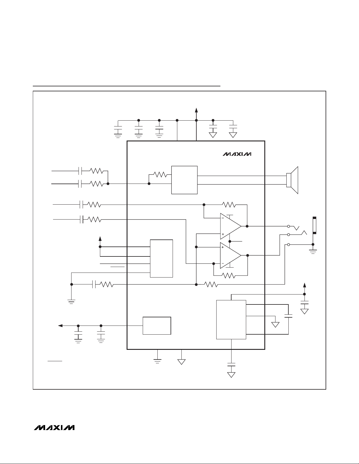
MAX9791/MAX9792
Windows Vista-Compliant Class D Speaker
Amplifiers with DirectDrive Headphone Amplifiers
______________________________________________________________________________________ 31
MAX9792C Block Diagram
TO CODEC
µC BEEP INPUT
2.0µF
C
C
IN3
IN1
C
IN2
C
IN2
R
IN3
RIN1
R
IN2
R
IN2
2.7V TO 5.5V
C
COM
2.0µF
R
COM
SPKR_IN
HP_INL
HP_INR
LDO_EN
HP_EN 22
BEEP 21
SPKR_EN
COM
LDO_OUT
2.7V TO 5.5V
1.0µF1.0µF
0.1µF
AVDD
PVDD
7
17, 26
0.1µF
10µF
MAX9792C
20kΩ
28
3
2
8
CONTROL
27
4
6
LDO BLOCK
MONO
CLASS D
AMPLIFIER
40.2kΩ
TO HPVDD
TO CPVSS
TO HPVDD
40.2kΩ
40.2kΩ
CHARGE
PUMP
19, 24 OUT+
OUT-
18, 25
10
HPL
HPR
9
SENSE
11
HPVDD
16
C1P
15
CPGND
14
C1N
13
2.7V TO 5.5V
C3
10µF
C1
1.0µF
NOTE: LOGIC PINS CONFIGURED FOR:
LDO_EN = 1, LDO ENABLED
SPKR_EN = 0, SPEAKER AMPLIFIER ENABLED
HP_EN = 1, HEADPHONE AMPLIFIER ENABLED
1, 5
20, 23
12
PGNDGND
CPVSS
C2
1.0µF

MAX9791/MAX9792
Windows Vista-Compliant Class D Speaker
Amplifiers with DirectDrive Headphone Amplifiers
32 ______________________________________________________________________________________
PACKAGE TYPE PACKAGE CODE OUTLINE NO. LAND PATTERN NO.
28 TQFN-EP T2844-1
21-0139 90-0068
Package Information
For the latest package outline information and land patterns, go to www.maxim-ic.com/packages. Note that a “+”, “#”, or “-” in the
package code indicates RoHS status only. Package drawings may show a different suffix character, but the drawing pertains to the
package regardless of RoHS status.

MAX9791/MAX9792
Windows Vista-Compliant Class D Speaker
Amplifiers with DirectDrive Headphone Amplifiers
______________________________________________________________________________________ 33
Package Information (continued)
For the latest package outline information and land patterns, go to www.maxim-ic.com/packages. Note that a “+”, “#”, or “-” in the
package code indicates RoHS status only. Package drawings may show a different suffix character, but the drawing pertains to the
package regardless of RoHS status.

MAX9791/MAX9792
Windows Vista-Compliant Class D Speaker
Amplifiers with DirectDrive Headphone Amplifiers
Maxim cannot assume responsibility for use of any circuitry other than circuitry entirely embodied in a Maxim product. No circuit patent licenses are
implied. Maxim reserves the right to change the circuitry and specifications without notice at any time.
34
____________________Maxim Integrated Products, 120 San Gabriel Drive, Sunnyvale, CA 94086 408-737-7600
© 2010 Maxim Integrated Products Maxim is a registered trademark of Maxim Integrated Products, Inc.
Revision History
REVISION
NUMBER
0 11/08 Initial release —
1 6/10 Adding MAX9791C/MAX9792C vers ion s
REVISION
DATE
DESCRIPTION
PAGES
CHANGED
1–7, 10, 13–16,
19, 21–30
 Loading...