

Page 1
MAX9789/MAX9790
Windows Vista-Compliant, Stereo Class AB Speaker
Amplifiers and DirectDrive Headphone Amplifiers
________________________________________________________________
Maxim Integrated Products
1
Ordering Information
19-0606; Rev 3; 9/09
For pricing, delivery, and ordering information, please contact Maxim Direct at 1-888-629-4642,
or visit Maxim’s website at www.maxim-ic.com.
General Description
The MAX9789/MAX9790 combine a stereo, 2W Class AB
speaker power amplifier with a stereo 100mW
DirectDrive
®
headphone amplifier in a single device. The
MAX9789/MAX9790 are designed for use with the
Microsoft Windows Vista
®
operating system and are fully
compliant with Microsoft’s Windows Vista specifications.
The headphone amplifier features Maxim’s DirectDrive
architecture that produces a ground-referenced output
from a single supply to eliminate the need for large DCblocking capacitors, as well as save cost, board space,
and component height. A high +90dB PSRR and low
0.002% THD+N ensures clean, low-distortion amplification of the audio signal.
Separate speaker and headphone amplifier control
inputs provide independent shutdown of the speaker
and headphone amplifiers, allowing speaker and headphone amplifiers to be active simultaneously, if
required. The industry-leading click-and-pop suppression circuitry reduces audible transients during startup
and shutdown cycles.
The MAX9789 features an internal LDO that can be used
as a clean power supply for a CODEC or other circuits.
The LDO output voltage is set internally at 4.75V or can
be adjusted between 1.21V and 4.75V using a simple
resistive divider. The LDO is protected against thermal
overloads and short circuits while providing 120mA of
continuous output current and can be enabled independently of the audio amplifiers.
By disabling the speaker and headphone amplifiers, and
the LDO (for MAX9789), the MAX9789/MAX9790 enter
low-power shutdown mode and draw only 0.3µA.
The MAX9789/MAX9790 operate from a single 4.5V to
5.5V supply and feature thermal-overload and output
short-circuit protection. Devices are specified over the
-40°C to +85°C extended temperature range.
Features
Applications
Note: All devices are specified over the -40°C to +85°C extended
temperature range.
+
Denotes a lead-free/RoHS-compliant package.
*
EP = Exposed pad.
**
Future product—contact factory for availability.
PART
PIN-PACKAGE
INTERNAL LDO
tON (ms)
MAX9789AETJ+
Yes 100
MAX9789BETJ+**
Yes 25
MAX9789CETJ+
Yes 100
MAX9790AETJ+
No 100
MAX9790BETJ+**
No 25
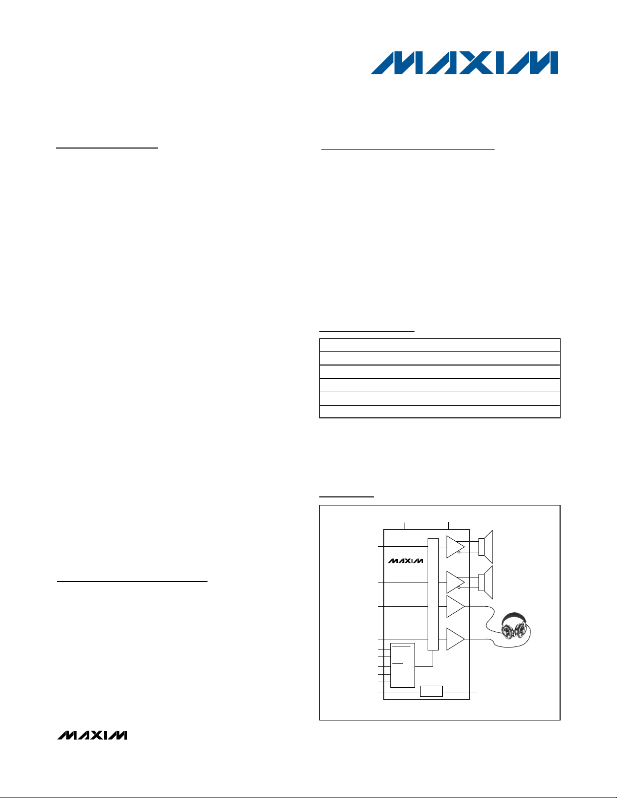
Simplified Block Diagrams
MAX9789
SPKR_EN
HP_EN
MUTE
GAIN1
GAIN2
SPEAKER SUPPLY
4.5V TO 5.5V
HEADPHONE SUPPLY
3.0V TO 5.5V
LDO
4.5V TO 5.5V
SPKR_INR
SPKR_INL
HP_INR
HP_INL
1.21V TO 4.75V
♦ Microsoft Windows Vista Compliant
♦ Class AB 2W Stereo BTL Speaker Amplifier
♦ 100mW DirectDrive Headphone Amplifier
Eliminates Costly, Bulky DC-Blocking Capacitors
♦ Excellent RF Immunity
♦ Integrated 120mA LDO (MAX9789)
♦ High +90dB PSRR, Low 0.002% THD+N
♦ Low-Power Shutdown Mode
♦ Click-and-Pop Suppression
♦ Short-Circuit and Thermal-Overload Protection
♦ Available in 32-Pin Thin QFN (5mm x 5mm x
0.8mm) Package
Notebook Computers
Tablet PCs
Portable Multimedia Players
Windows Vista is a registered trademark of Microsoft Corp.
Pin Configurations appear at end of data sheet.
Simplified Block Diagrams continued at end of data sheet.
DirectDrive is a registered trademark of Maxim Integrated
Products, Inc.
32 TQFN-EP*
32 TQFN-EP*
32 TQFN-EP*
32 TQFN-EP*
32 TQFN-EP*
Page 2
MAX9789/MAX9790
Windows Vista-Compliant, Stereo Class AB Speaker
Amplifiers and DirectDrive Headphone Amplifiers
2 _______________________________________________________________________________________
ABSOLUTE MAXIMUM RATINGS
ELECTRICAL CHARACTERISTICS
(VDD= PVDD= CPVDD= HPVDD= HP_EN = V
LDO_EN
(MAX9789 only) = +5V, V
GND
= V
PGND
= V
CPGND
= SPKR_EN = V
LDO_SET
(MAX9789 only) = 0V, I
LDO_OUT
(MAX9789 only) = 0, C1 = C2 = C
BIAS
= 1µF. RL= ∞, unless otherwise specified, V
GAIN1
= 0,
V
GAIN2
= 5V (A
VSP
= 10dB, A
VHP
= 3.5dB), TA= T
MIN
to T
MAX
, unless otherwise noted. Typical values are at TA= +25°C.) (Note 2)
Stresses beyond those listed under “Absolute Maximum Ratings” may cause permanent damage to the device. These are stress ratings only, and functional
operation of the device at these or any other conditions beyond those indicated in the operational sections of the specifications is not implied. Exposure to
absolute maximum rating conditions for extended periods may affect device reliability.
Supply Voltage (VDD, PVDD, HPVDD,
CPV
DD
to GND)..................................................-0.3V to +6.0V
GND to PGND, CPGND ......................................................±0.3V
CPV
SS
, C1N, VSSto GND......................................-6.0V to +0.3V
HPR, HPL to GND ...............................................................±3.0V
Any Other Pin .............................................-0.3V to (V
DD
+ 0.3V)
Duration of OUT_+, OUT_- Short Circuit
to GND or PV
DD
......................................................Continuous
Duration of Short Circuit between OUT_+, OUT_-
and LDO_OUT.........................................................Continuous
Duration of Short Circuit between HPR, HPL and GND,
V
SS
or HPVDD..........................................................Continuous
Continuous Current (PV
DD
, OUT_+, OUT_-, PGND).............1.7A
Continuous Current (CPV
DD
, C1N, C1P, CPVSS, PVSS,
V
DD,
HPVDD, LDO_OUT, HPR, HPL) .............................850mA
Continuous Input Current (all other pins) .........................±20mA
Continuous Power Dissipation (T
A
= +70°C)
32-Pin Thin QFN Single-Layer Board
(derate 18.6mW/°C above +70°C)..............................1489mW
θ
JA
...........................................................................53.7°C/W
θ
JC
...........................................................................19.9°C/W
32-Pin Thin QFN Multilayer Board
(derate 24.9 mW/°C above +70°C).............................1990mW
θ
JA
...........................................................................40.2°C/W
θ
JC
...........................................................................19.9°C/W
Operating Temperature Range ...........................-40°C to +85°C
Junction Temperature......................................................+150°C
Storage Temperature Range .............................-65°C to +150°C
Lead Temperature (soldering, 10s) .................................+300°C
Note 1: Package thermal resistances were obtained using the method described in JEDEC specification JESD51-7 using a four-
layer board. For detailed information on package thermal considerations, refer to www.maxim-ic.com/thermal-tutorial
.
PARAMETER SYMBOL CONDITIONS MIN TYP MAX UNITS
GENERAL
Supply Voltage VDD, PV
Headphone Supply Voltage
Quiescent Current I
Shutdown Current I
Bias Voltage V
Shutdown to Full Operation t
Gain Switching Time t
CPV
HPV
SHDN
DD
DD
DD
DD
BIAS
SON
SW
Channel-to-Channel Gain
Tracking
SPEAKER AMPLIFIER
Output Power P
Total Harmonic Distortion Plus
Noise
OUT
THD+N
,
Guaranteed by PSRR and LDO Line
Regulation Tests
Guaranteed by PSRR Test 3.0 5.5 V
SPKR_EN HP_EN
1 (MAX9789) 0 (MAX9789) 0.1 0.4 mA
1 (MAX9790) 0 (MAX9790) 0.3 6 µA
11 713
0 0 14 29
0 1 18 40
SPKR_EN = VDD, HP_EN = LDO_EN = GND 0.3 6 µA
MAX9789A/MAX9789C/MAX9790A 100
MAX9789B/MAX9790B 25
THD+N = 1%, f = 1kHz,
T
= +25°C
A
RL = 8Ω, P
R
= 4Ω, P
L
4.5 5.5 V
1.7 1.8 1.9 V
10 µs
±0.1 dB
RL = 4Ω 2
R
= 8Ω 1
L
= 1W, f = 1kHz 0.002
OUT
= 1W, f = 1kHz 0.004
OUT
mA
ms
W
%
Page 3
MAX9789/MAX9790
Windows Vista-Compliant, Stereo Class AB Speaker
Amplifiers and DirectDrive Headphone Amplifiers
_______________________________________________________________________________________ 3
ELECTRICAL CHARACTERISTICS (continued)
(VDD= PVDD= CPVDD= HPVDD= HP_EN = V
LDO_EN
(MAX9789 only) = +5V, V
GND
= V
PGND
= V
CPGND
= SPKR_EN = V
LDO_SET
(MAX9789 only) = 0V, I
LDO_OUT
(MAX9789 only) = 0, C1 = C2 = C
BIAS
= 1µF. RL= ∞, unless otherwise specified, V
GAIN1
= 0,
V
GAIN2
= 5V (A
VSP
= 10dB, A
VHP
= 3.5dB), TA= T
MIN
to T
MAX
, unless otherwise noted. Typical values are at TA= +25°C.) (Note 2)
PARAMETER SYMBOL CONDITIONS MIN TYP MAX UNITS
Power-Supply Rejection Ratio PSRR
Voltage Gain A
Input Impedance R
Output Offset Voltage V
V
IN
OS
VDD = 4.5V to 5.5V, TA = +25°C 72 90
f = 1kHz, 200mV
P-P
f = 10kHz, 200mV
GAIN1 GAIN2
00 6
01 10
1 0 15.6
1 1 21.6
Measured at speaker amplifier inputs
GAIN1 GAIN2
00 80
01 65
10 45
11 25
Measured between
OUT_+ and OUT_-,
T
= +25°C
A
(Note 4) 70
(Note 4) 50
P-P
MAX9789C ±1 ±25
±1 ±15
dB
dB
kΩ
mV
RL = 8Ω, peak voltage,
Click-and-Pop Level K
A-weighted, 32 samples
CP
per second (Notes 3, 4)
Signal-to-Noise Ratio SNR RL = 8Ω, P
Noise V
Capacitive-Load Drive C
BW = 22Hz to 22kHz 30 µV
n
No sustained oscillations 200 pF
L
L to R, R to L, R
= 70.7nV
Crosstalk
V
OUT
= 1W
OUT
= 8Ω, FS = 0.707V
L
RMS,
Into shutdown -50
Out of shutdown -50
A-weighted 102
f = 22Hz to 22kHz 99
,
RMS
20kHz AES17,
dBV
dB
RMS
-70 dB
BW = 20Hz to 20kHz
Slew Rate SR 1.4 V/µs
HEADPHONE AMPLIFIER
Output Power P
OUT
THD+N = 1%, f =
1kHz, T
= +25°C
A
RL = 32Ω, FS = 0.300V
= 210mV
V
OUT
RMS
RL = 16Ω 100
R
= 32Ω 55
L
,
RMS
, 20kHz AES17,
mW
-77 dB FS
BW = 20Hz to 20kHz
Total Harmonic Distortion Plus
Noise
THD+N
RL = 32Ω, P
RL = 16Ω, P
= 10kΩ, FS = 0.707V
R
L
V
= 500mV
OUT
= 40mW, f = 1kHz 0.02
OUT
= 60mW, f = 1kHz 0.03
OUT
,
RMS
, 20kHz AES17,
RMS
%
-94 dB FS
BW = 20Hz to 20kHz
Page 4
MAX9789/MAX9790
Windows Vista-Compliant, Stereo Class AB Speaker
Amplifiers and DirectDrive Headphone Amplifiers
4 _______________________________________________________________________________________
ELECTRICAL CHARACTERISTICS (continued)
(VDD= PVDD= CPVDD= HPVDD= HP_EN = V
LDO_EN
(MAX9789 only) = +5V, V
GND
= V
PGND
= V
CPGND
= SPKR_EN = V
LDO_SET
(MAX9789 only) = 0V, I
LDO_OUT
(MAX9789 only) = 0, C1 = C2 = C
BIAS
= 1µF. RL= ∞, unless otherwise specified, V
GAIN1
= 0,
V
GAIN2
= 5V (A
VSP
= 10dB, A
VHP
= 3.5dB), TA= T
MIN
to T
MAX
, unless otherwise noted. Typical values are at TA= +25°C.) (Note 2)
PARAMETER SYMBOL CONDITIONS MIN TYP MAX UNITS
Power-Supply Rejection Ratio PSRR
Voltage Gain A
Input Impedance R
Output Offset Voltage V
Click-and-Pop Level K
Dynamic Range DR
V
IN
OS
CP
Signal-to-Noise Ratio SNR
Noise V
Capacitive-Load Drive C
n
L
Crosstalk
Slew Rate SR 0.4 V/µs
Charge-Pump Frequency f
OSC
LOW-DROPOUT LINEAR REGULATOR
Regulator Input Voltage Range V
Ground Current I
Output Current I
DD
GND
OUT
Crosstalk
Fixed Output Voltage Accuracy I
Adjustable Output Voltage Range 1.21 4.75 V
LDO_SET Reference Voltage V
SET
LDO_SET Dual-Mode Threshold 200 mV
HPVDD = 3V to 5.5V, TA = +25°C 70 95
f = 1kHz, V
f = 10kHz, V
RIPPLE
RIPPLE
= 200mV
= 200mV
(Note 4) 84
P-P
(Note 4) 63
P-P
3.5 dB
Measured at headphone amplifier inputs 20 40 80 kΩ
TA = +25°C
RL = 32Ω, peak voltage,
MAX9789C ±2 ±10
Into shutdown -60
±2 ±7
A-weighted, 32 samples
per second (Notes 3, 4)
RL = 32Ω, f = 1kHz, A-weighted,
FS = 0.300V
R
= 10kΩ, f = 1kHz, A-weighted,
L
FS = 0.707V
R
= 32Ω,
L
= 60mW
P
OUT
RMS
RMS
, V
, V
Out of shutdown -60
= 300µV
OUT
OUT
= 707µV
RMS
RMS
22Hz to 22kHz 100
A-weighted 103
89
97
BW = 22Hz to 22kHz 12 µV
No sustained oscillations 200 pF
RL = 32Ω,
L to R, R to L,
20kHz AES17
BW = 20Hz to 20kHz
FS = 0.300V
= 30mV
V
OUT
= 10kΩ,
R
L
FS = 0.707V
= 70.7mV
V
OUT
RMS
RMS
RMS
,
,
RMS
-74
-77
500 550 625
MAX9789C 475 550 625
Inferred from line regulation 4.5 5.5 V
I
= 0mA 0.1 0.4
OUT
I
= 120mA -40
OUT
120 mA
V
= 4.75V, I
OUT
speaker P
= 1mA
OUT
OUT
= 0mA, f = 1kHz,
OUT
= 2W, speaker RL = 4Ω
MAX9789C ±3.0
-95 dB
±1.5
1.18 1.21 1.23
MAX9789C 1.18 1.21 1.25
dB
mV
dBV
dB FS
dB
RMS
dB
kHz
mA
%
V
Page 5
MAX9789/MAX9790
Windows Vista-Compliant, Stereo Class AB Speaker
Amplifiers and DirectDrive Headphone Amplifiers
_______________________________________________________________________________________ 5
Note 2: All devices are 100% production tested at room temperature. All temperature limits are guaranteed by design.
Note 3: Specified at room temperature with an 8Ω resistive load connected across BTL output for speaker amplifier. Specified at
room temperature with a 32Ω resistive load connected between HPR, HPL, and GND for headphone amplifier. Speaker and
headphone mode transitions are controlled by SPKR_EN and HP_EN control pins, respectively.
Note 4: Amplifier inputs AC-coupled to GND.
Note 5: Maximum value is due to test limitations.
Note 6: V
LDO_OUT
= V
LDO_OUTNOMINAL
- 2%.
ELECTRICAL CHARACTERISTICS (continued)
(VDD= PVDD= CPVDD= HPVDD= HP_EN = V
LDO_EN
(MAX9789 only) = +5V, V
GND
= V
PGND
= V
CPGND
= SPKR_EN = V
LDO_SET
(MAX9789 only) = 0V, I
LDO_OUT
(MAX9789 only) = 0, C1 = C2 = C
BIAS
= 1µF. RL= ∞, unless otherwise specified, V
GAIN1
= 0,
V
GAIN2
= 5V (A
VSP
= 10dB, A
VHP
= 3.5dB), TA= T
MIN
to T
MAX
, unless otherwise noted. Typical values are at TA= +25°C.) (Note 2)
PARAMETER SYMBOL CONDITIONS MIN TYP MAX UNITS
LDO_SET Input Bias Current
(Note 5)
Dropout Voltage (Note 6) V
Current Limit I
I
SET
LIM
DO
Startup Time 20 µs
Line Regulation
Load Regulation
Ripple Rejection
Output Voltage Noise
DIGITAL INPUTS (SPKR_EN, HP_EN, MUTE, GAIN1, GAIN2, LDO_EN (MAX9789 Only))
Input-Voltage High V
Input-Voltage Low V
INH
INL
Input Bias Current ±1 µA
V
= 4.75V (fixed
OUT
I
output operation),
T
= +25°C
A
V
= 4.5V to 5.5V, LDO_OUT = 2.5V,
IN
I
LDO_OUT
V
LDO_OUT
1mA < I
V
RIPPLE
I
LDO_OUT
20Hz to 22kHz, C
I
LDO_OUT
= 1mA
= 4.75V,
LDO_OUT
= 200mV
= 10mA
= 120mA
< 120mA
P-P
LDO_OUT
I
f = 1kHz 59
f = 10kHz 42
= 2 x 1µF,
±20 ±500 nA
= 50mA 25 50
OUT
= 120mA 75 150
OUT
300 mA
-4.8 +0.8 +4.8 mV/V
0.2 mV/mA
125 µV
2V
0.8 V
mV
dB
RMS
Page 6
MAX9789/MAX9790
Windows Vista-Compliant, Stereo Class AB Speaker
Amplifiers and DirectDrive Headphone Amplifiers
6 _______________________________________________________________________________________
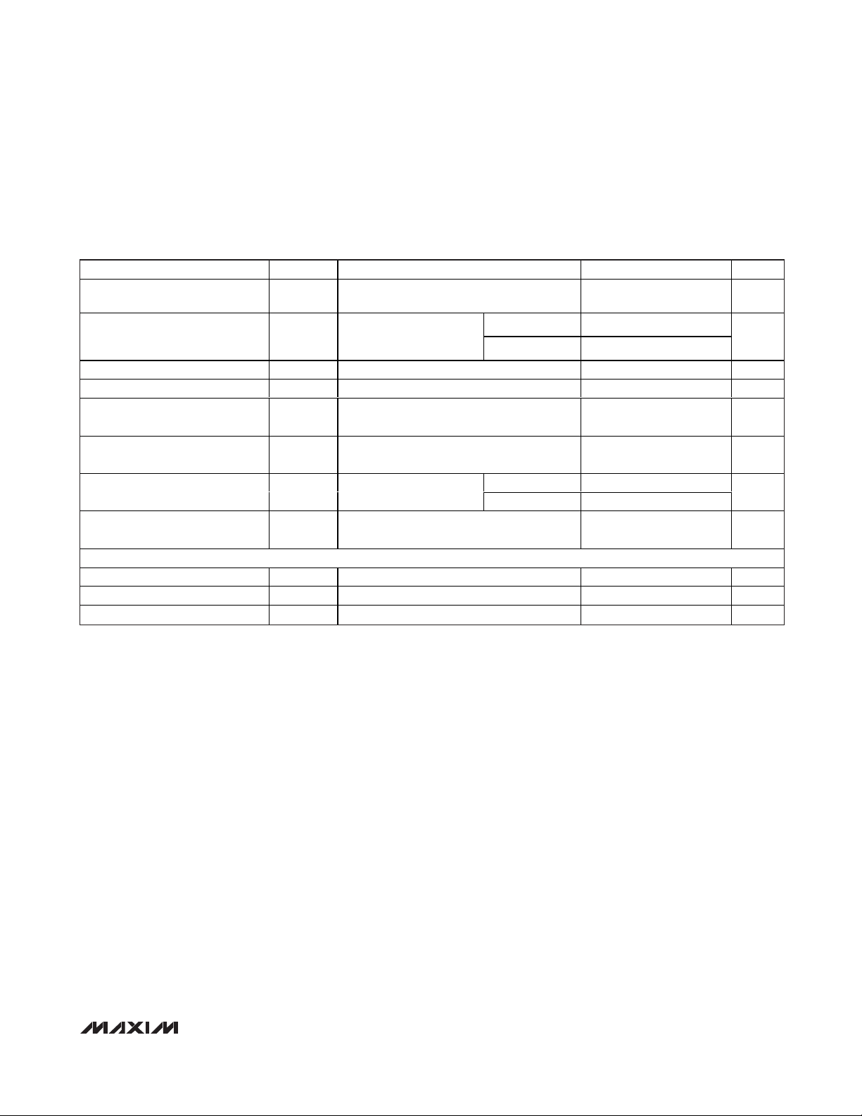
Typical Operating Characteristics
(VDD= PVDD= CPVDD= HPVDD= LDO_EN = +5V, V
GND
= V
PGND
= V
CPGND
= V
LDO_SET
= 0V, C1 = C2 = C
BIAS
= CIN= 1µF. RL=
∞, unless otherwise specified, GAIN1 = 0, GAIN2 = 1 (A
VSP
= 10dB, A
VHP
= 3.5dB), measurement BW = 20kHz AES17, TA= +25°C,
unless otherwise noted. Headphone mode: SPKR_EN = 1, HP_EN = 0. Speaker mode: SPKR_EN = 0, HP_EN = 1.)
TOTAL HARMONIC DISTORTION PLUS NOISE
vs. FREQUENCY (HEADPHONE MODE)
MAX9789 toc01
FREQUENCY (Hz)
THD+N (dB FS)
10k1k100
-100
-90
-80
-70
-60
-110
10 100k
FS = 0.707V
RMS
V
OUT
= -3dB FS
R
L
= 10k
Ω
TOTAL HARMONIC DISTORTION PLUS NOISE
vs. FREQUENCY (HEADPHONE MODE)
MAX9789 toc02
FREQUENCY (Hz)
THD+N (dB FS)
10k1k100
-90
-80
-70
-60
-100
10 100k
HPVDD = 3V
FS = 0.707V
RMS
V
OUT
= -3dB FS
R
L
= 10k
Ω
TOTAL HARMONIC DISTORTION PLUS NOISE
vs. OUTPUT VOLTAGE (HEADPHONE MODE)
MAX9789 toc03
OUTPUT VOLTAGE (V
RMS
)
THD+N (%)
1.51.00.5
0.01
0.1
1
10
0.001
0 2.0
RL = 10k
Ω
fIN = 20Hz
fIN = 10kHz
fIN = 1kHz
TOTAL HARMONIC DISTORTION PLUS NOISE
vs. OUTPUT VOLTAGE (HEADPHONE MODE)
MAX9789 toc04
OUTPUT VOLTAGE (V
RMS
)
THD+N (%)
1.51.00.5
0.01
0.1
1
10
0.001
0 2.0
HPVDD = 3V
R
L
= 10k
Ω
fIN = 20Hz
fIN = 1kHz
fIN = 10kHz
CROSSTALK
vs. FREQUENCY (HEADPHONE MODE)
MAX9789 toc05
FREQUENCY (Hz)
CROSSTALK (dB)
10k1k100
-80
-90
-60
-40
-20
-70
-50
-30
-10
0
-100
10 100k
FS = 0.707V
RMS
V
OUT
= -20dB FS
R
L
= 10k
Ω
LEFT TO RIGHT
RIGHT TO LEFT
HEADPHONE OUTPUT SPECTRUM
MAX9789 toc06
FREQUENCY (Hz)
CROSSTALK (dB)
15k10k5k
-80
-90
-60
-40
-20
-70
-50
-30
-10
0
-140
-100
-110
-120
-130
0 20k
FS = 0.300V
RMS
V
OUT
= -60dB FS
R
L
= 10k
Ω
TOTAL HARMONIC DISTORTION PLUS NOISE
vs. FREQUENCY (SPEAKER MODE)
MAX9789 toc07
FREQUENCY (Hz)
THD+N (dB FS)
1k100
-90
-95
-85
-80
-75
-100
10 100k10k
V
OUT
= -3dB FS
FS = 0.707V
RMS
RL = 3Ω
TOTAL HARMONIC DISTORTION PLUS NOISE
vs. FREQUENCY (SPEAKER MODE)
MAX9789 toc08
FREQUENCY (Hz)
THD+N (dB FS)
1k100
-90
-95
-85
-80
-75
-100
10 100k10k
V
OUT
= -3dB FS
FS = 0.707V
RMS
RL = 4Ω
TOTAL HARMONIC DISTORTION PLUS NOISE
vs. FREQUENCY (SPEAKER MODE)
MAX9789 toc09
FREQUENCY (Hz)
THD+N (dB FS)
1k100
-90
-100
-95
-105
-85
-80
-75
-110
10 100k10k
V
OUT
= -3dB FS
FS = 0.707V
RMS
RL = 8Ω
Page 7
MAX9789/MAX9790
Windows Vista-Compliant, Stereo Class AB Speaker
Amplifiers and DirectDrive Headphone Amplifiers
_______________________________________________________________________________________
7
Typical Operating Characteristics (continued)
(VDD= PVDD= CPVDD= HPVDD= LDO_EN = +5V, V
GND
= V
PGND
= V
CPGND
= V
LDO_SET
= 0V, C1 = C2 = C
BIAS
= CIN= 1µF. RL=
∞, unless otherwise specified, GAIN1 = 0, GAIN2 = 1 (A
VSP
= 10dB, A
VHP
= 3.5dB), measurement BW = 20kHz AES17, TA= +25°C,
unless otherwise noted. Headphone mode: SPKR_EN = 1, HP_EN = 0. Speaker mode: SPKR_EN = 0, HP_EN = 1.)
TOTAL HARMONIC DISTORTION PLUS NOISE
vs. OUTPUT POWER (SPEAKER MODE)
MAX9789 toc10
OUTPUT POWER (W)
THD+N (%)
1.51.00.5
0.01
0.1
1
10
0.001
0 3.02.0 2.5
RL = 3
Ω
fIN = 10kHz
fIN = 20Hz
fIN = 1kHz
TOTAL HARMONIC DISTORTION PLUS NOISE
vs. OUTPUT POWER (SPEAKER MODE)
MAX9789 toc11
OUTPUT POWER (W)
THD+N (%)
1.51.00.5
0.01
0.1
1
10
0.001
0 2.52.0
RL = 4
Ω
fIN = 10kHz
fIN = 20Hz
fIN = 1kHz
TOTAL HARMONIC DISTORTION PLUS NOISE
vs. OUTPUT POWER (SPEAKER MODE)
MAX9789 toc12
OUTPUT POWER (W)
THD+N (%)
1.00.5
0.01
0.1
1
10
0.001
01.5
RL = 8
Ω
fIN = 10kHz
fIN = 20Hz
fIN = 1kHz
CROSSTALK
vs. FREQUENCY (SPEAKER MODE)
MAX9789 toc13
FREQUENCY (Hz)
CROSSTALK (dB)
10k1k100
-80
-60
-40
-20
0
-100
-70
-50
-30
-10
-90
10 100k
FS = 0.707V
RMS
V
OUT
= -20dB FS
R
L
= 8
Ω
LEFT TO RIGHT
RIGHT TO LEFT
SPEAKER OUTPUT SPECTRUM
FREQUENCY (Hz)
CROSSTALK (dB)
MAX9789 toc14
0 5k 10k 15k 20k
-140
-130
-120
-110
-100
-90
-80
-70
-60
-50
-40
-30
-20
-10
0
FS = 0.707V
RMS
V
OUT
= -60dB FS
R
L
= 8Ω
OUTPUT POWER vs. LOAD RESISTANCE
(SPEAKER MODE)
RL (Ω)
OUTPUT POWER (W)
MAX9789 toc15
0
0.5
1.0
1.5
2.0
2.5
3.0
3.5
1 10 100
fIN = 1kHz
THD+N = 1%
THD+N = 10%
POWER DISSIPATION PER CHANNEL
vs. OUTPUT POWER (SPEAKER MODE)
OUTPUT POWER PER CHANNEL (W)
POWER DISSIPATION PER CHANNEL (W)
MAX9789 toc16
0 0.5 1.0 1.5 2.0
0
0.25
0.50
0.75
1.00
1.25
1.50
RL = 8Ω
RL = 4Ω
fIN = 1kHz
POWER-SUPPLY REJECTION RATIO
(SPEAKER MODE)
FREQUENCY (Hz)
PSRR (dB)
MAX9789 toc17
10 100 1k 10k 100k
100
-90
-70
-80
-40
-50
-60
-30
-20
-10
0
V
RIPPLE
= 200mV
P-P
OUTPUT REFERRED
Page 8
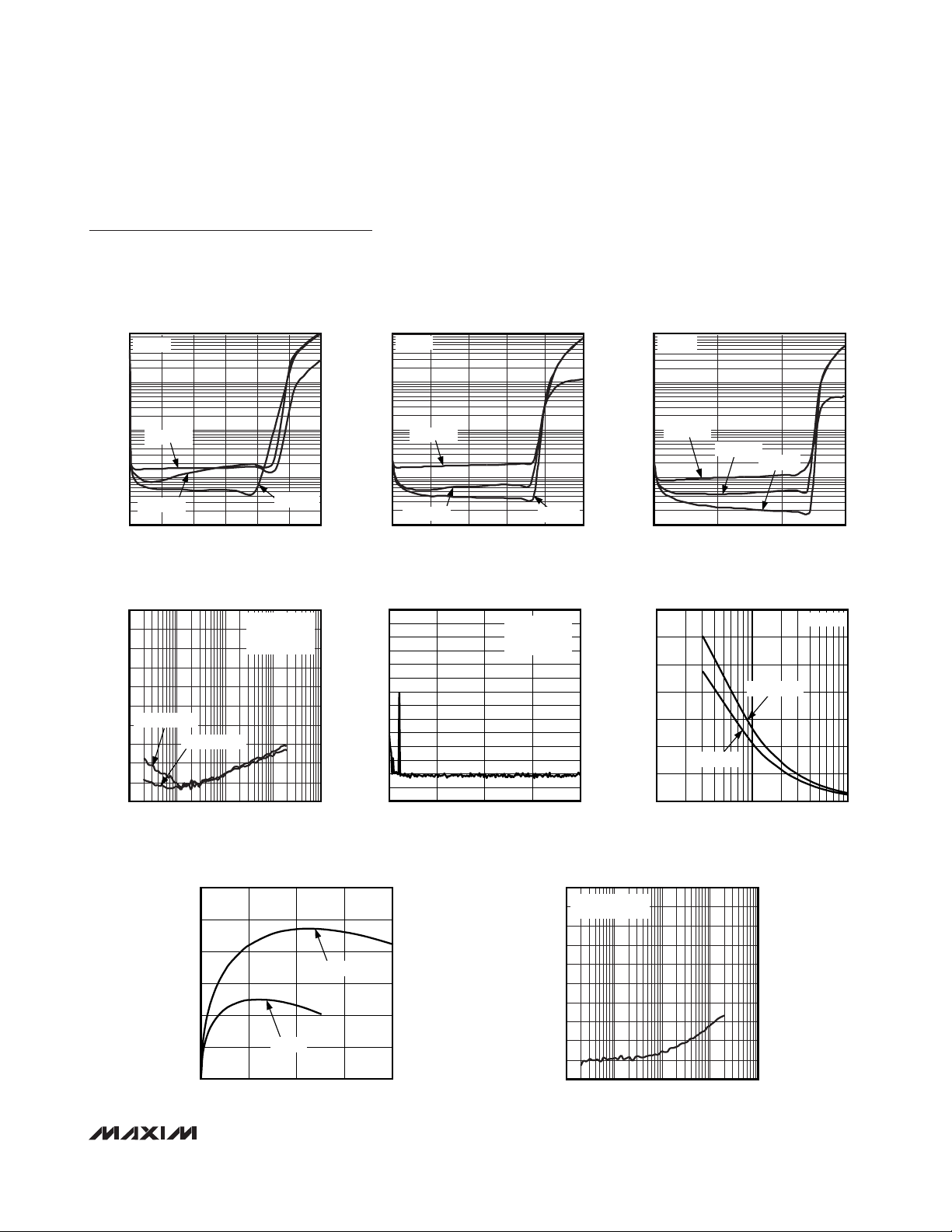
SPEAKER SHUTDOWN WAVEFORM
MAX9789 toc20
20ms/div
2V/div
5V/div
100mV/div
OUT_+ AND OUT_-
OUT_+ - OUT_-
SPKR_EN
Typical Operating Characteristics (continued)
(VDD= PVDD= CPVDD= HPVDD= LDO_EN = +5V, V
GND
= V
PGND
= V
CPGND
= V
LDO_SET
= 0V, C1 = C2 = C
BIAS
= CIN= 1µF. RL=
∞, unless otherwise specified, GAIN1 = 0, GAIN2 = 1 (A
VSP
= 10dB, A
VHP
= 3.5dB), measurement BW = 20kHz AES17, TA= +25°C,
unless otherwise noted. Headphone mode: SPKR_EN = 1, HP_EN = 0. Speaker mode: SPKR_EN = 0, HP_EN = 1.)
MAX9789/MAX9790
Windows Vista-Compliant, Stereo Class AB Speaker
Amplifiers and DirectDrive Headphone Amplifiers
8 _______________________________________________________________________________________
SPEAKER STARTUP WAVEFORM
MAX9789A/MAX9789C/MAX9790A
MAX9789 toc18
SPKR_EN
5V/div
OUT_+ AND OUT_2V/div
SPEAKER STARTUP WAVEFORM
MAX9789B/MAX9790B
MAX9789 toc19
SPKR_EN
5V/div
OUT_+ AND OUT_2V/div
20ms/div
TOTAL HARMONIC DISTORTION PLUS NOISE
vs. FREQUENCY (HEADPHONE MODE)
-65
-70
-75
V
= -3dB FS
-80
-85
-90
THD+N (dB FS)
-95
-100
-105
-110
OUT
HPVDD = 3V
FS = 0.300V
RL = 32Ω
10 100k
RMS
FREQUENCY (Hz)
10k1k100
MAX9789 toc22
OUT_+ - OUT_100mV/div
TOTAL HARMONIC DISTORTION PLUS NOISE
-65
-70
-75
-80
-85
-90
THD+N (dB FS)
-95
-100
-105
-110
10 100k
TOTAL HARMONIC DISTORTION PLUS NOISE
vs. FREQUENCY (HEADPHONE MODE)
-65
-70
-75
V
= -3dB FS
OUT
-80
-85
-90
THD+N (dB FS)
-95
-100
FS = 0.300V
-105
-110
10 100k
RL = 16Ω
RMS
10k1k100
FREQUENCY (Hz)
20ms/div
vs. FREQUENCY (HEADPHONE MODE)
V
= -3dB FS
OUT
FS = 0.300V
RMS
Ω
RL = 32
10k1k100
FREQUENCY (Hz)
TOTAL HARMONIC DISTORTION PLUS NOISE
vs. FREQUENCY (HEADPHONE MODE)
-65
-70
MAX9789 toc23
-75
V
= -3dB FS
OUT
-80
-85
-90
THD+N (dB FS)
-95
-100
HPVDD = 3V
FS = 0.300V
-105
-110
10 100k
RL = 16Ω
RMS
OUT_+ - OUT_100mV/div
MAX9789 toc21
FREQUENCY (Hz)
MAX9789 toc24
10k1k100
Page 9
MAX9789/MAX9790
HEADPHONE OUTPUT SPECTRUM
MAX9789 toc30
FREQUENCY (kHz)
AMPLITUDE (dB)
15105
-80
-60
-40
-20
0
-140
-70
-50
-30
-10
-100
-120
-90
-110
-130
020
FS = 0.707V
RMS
V
OUT
= -60dB FS
R
L
= 32
Ω
OUTPUT POWER vs. LOAD RESISTANCE
(HEADPHONE MODE)
RL (Ω)
OUTPUT POWER (mW)
MAX9789 toc31
0
50
100
150
10 100 1000
THD+N = 1%
THD+N = 10%
fIN = 1kHz
OUTPUT POWER vs. LOAD RESISTANCE
(HEADPHONE MODE)
RL (Ω)
OUTPUT POWER (mW)
MAX9789 toc32
0
50
100
10 100 1000
HPVDD = 3V
f
IN
= 1kHz
THD+N = 1%
THD+N = 10%
Typical Operating Characteristics (continued)
(VDD= PVDD= CPVDD= HPVDD= LDO_EN = +5V, V
GND
= V
PGND
= V
CPGND
= V
LDO_SET
= 0V, C1 = C2 = C
BIAS
= CIN= 1µF. RL=
∞, unless otherwise specified, GAIN1 = 0, GAIN2 = 1 (A
VSP
= 10dB, A
VHP
= 3.5dB), measurement BW = 20kHz AES17, TA= +25°C,
unless otherwise noted. Headphone mode: SPKR_EN = 1, HP_EN = 0. Speaker mode: SPKR_EN = 0, HP_EN = 1.)
TOTAL HARMONIC DISTORTION PLUS NOISE
vs. OUTPUT POWER (HEADPHONE MODE)
MAX9789 toc26
OUTPUT POWER (mW)
THD+N (%)
604020
0.1
10
0.01
1
010080
RL = 32
Ω
f = 1kHz
f = 10kHz
f = 20Hz
CROSSTALK
vs. FREQUENCY (HEADPHONE MODE)
MAX9789 toc29
FREQUENCY (Hz)
CROSSTALK (dB)
10k1k100
-80
-60
-40
-20
0
-110
-70
-50
-30
-10
-90
-100
10 100k
FS = 0.300V
RMS
V
OUT
= -20dB FS
R
L
= 32
Ω
LEFT TO RIGHT
RIGHT TO LEFT
Windows Vista-Compliant, Stereo Class AB Speaker
Amplifiers and DirectDrive Headphone Amplifiers
_______________________________________________________________________________________
9
TOTAL HARMONIC DISTORTION PLUS NOISE
vs. OUTPUT POWER (HEADPHONE MODE)
10
MAX9789 toc25
1
THD+N (%)
0.1
0.01
f = 20Hz
f = 1kHz
0200
OUTPUT POWER (mW)
f = 10kHz
15010050
RL = 16
Ω
TOTAL HARMONIC DISTORTION PLUS NOISE
vs. OUTPUT POWER (HEADPHONE MODE)
10
MAX9789 toc28
1
THD+N (%)
0.1
f = 20Hz
f = 1kHz
f = 10kHz
TOTAL HARMONIC DISTORTION PLUS NOISE
vs. OUTPUT POWER (HEADPHONE MODE)
10
1
f = 20Hz
THD+N (%)
0.1
0.01
0150
OUTPUT POWER (mW)
f = 10kHz
f = 1kHz
HPVDD = 3V
Ω
= 16
R
L
10050
MAX9789 toc27
HPVDD = 3V
Ω
= 32
R
0.01
010080
OUTPUT POWER (mW)
604020
L
Page 10

MAX9789/MAX9790
Windows Vista-Compliant, Stereo Class AB Speaker
Amplifiers and DirectDrive Headphone Amplifiers
10 ______________________________________________________________________________________
Typical Operating Characteristics (continued)
(VDD= PVDD= CPVDD= HPVDD= LDO_EN = +5V, V
GND
= V
PGND
= V
CPGND
= V
LDO_SET
= 0V, C1 = C2 = C
BIAS
= CIN= 1µF. RL=
∞, unless otherwise specified, GAIN1 = 0, GAIN2 = 1 (A
VSP
= 10dB, A
VHP
= 3.5dB), measurement BW = 20kHz AES17, TA= +25°C,
unless otherwise noted. Headphone mode: SPKR_EN = 1, HP_EN = 0. Speaker mode: SPKR_EN = 0, HP_EN = 1.)
POWER DISSIPATION vs. OUTPUT POWER
(HEADPHONE MODE)
300
275
250
225
200
175
150
125
100
75
50
POWER DISSIPATION PER CHANNEL (mW)
25
0
0 25 50 75 100 125
OUTPUT POWER PER CHANNEL (mW)
RL = 16Ω
RL = 32Ω
HEADPHONE OUTPUT POWER vs. HPV
125
100
75
50
25
HEADPHONE OUTPUT POWER (mW)
THD+N = 1%
f
= 1kHz
IN
0
3.0 3.5 4.0 4.5 5.0
RL = 16Ω
HPV
(V)
DD
RL = 32Ω
MAX9789 toc33
DD
MAX9789 toc35
POWER DISSIPATION PER CHANNEL
vs. OUTPUT POWER (HEADPHONE MODE)
125
HPVDD = 3V
100
75
50
25
POWER DISSIPATION PER CHANNEL (mW)
0
0 20406080
OUTPUT POWER PER CHANNEL (mW)
RL = 16Ω
RL = 32Ω
POWER-SUPPLY REJECTION RATIO
vs. FREQUENCY (HEADPHONE MODE)
0
V
= 200mV
RIPPLE
-10
OUTPUT REFERRED
-20
-30
-40
-50
PSRR (dB)
-60
-70
-80
-90
-100
10 100 1k 10k 100k
P-P
FREQUENCY (Hz)
MAX9789 toc34
MAX9789 toc36
HEADPHONE STARTUP WAVEFORM
MAX9789A/MAX9789C/MAX9790A
20ms/div
MAX9789 toc37
HP_EN
5V/div
HP_
500mV/div
HEADPHONE STARTUP WAVEFORM
MAX9789B/MAX9790B
20ms/div
MAX9789 toc38
HP_EN
5V/div
HP_
500mV/div
Page 11

MAX9789/MAX9790
Windows Vista-Compliant, Stereo Class AB Speaker
Amplifiers and DirectDrive Headphone Amplifiers
______________________________________________________________________________________
11
Typical Operating Characteristics (continued)
(VDD= PVDD= CPVDD= HPVDD= LDO_EN = +5V, V
GND
= V
PGND
= V
CPGND
= V
LDO_SET
= 0V, C1 = C2 = C
BIAS
= CIN= 1µF. RL=
∞, unless otherwise specified, GAIN1 = 0, GAIN2 = 1 (A
VSP
= 10dB, A
VHP
= 3.5dB), measurement BW = 20kHz AES17, TA= +25°C,
unless otherwise noted. Headphone mode: SPKR_EN = 1, HP_EN = 0. Speaker mode: SPKR_EN = 0, HP_EN = 1.)
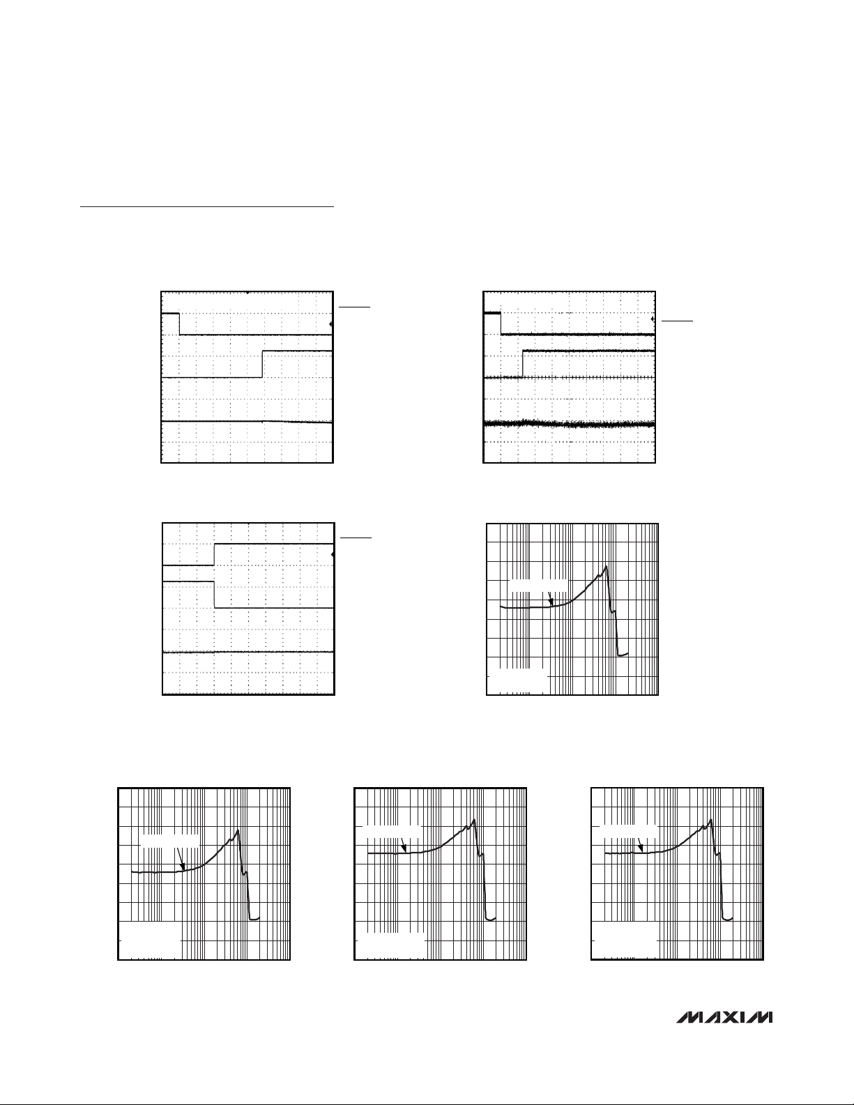
HEADPHONE SHUTDOWN WAVEFORM
MAX9789 toc39
20ms/div
HP_
HP_EN
5V/div
500mV/div
SUPPLY CURRENT vs. SUPPLY VOLTAGE
SUPPLY VOLTAGE (V)
SUPPLY CURRENT (mA)
MAX9789 toc40
4.50 4.75 5.00 5.25 5.50
-5
0
5
10
15
20
SPKR_EN = 0
HP_EN = 0
SPKR_EN = 0
HP_EN = 1
SPKR_EN = 1
HP_EN = 0
SPKR_EN = 1
HP_EN = 1
SHUTDOWN CURRENT vs. SUPPLY VOLTAGE
SUPPLY VOLTAGE (V)
SHUTDOWN CURRENT (μA)
MAX9789 toc41
4.50 4.75 5.00 5.25 5.50
0
0.1
0.2
0.3
SPKR_EN = 5V
HP_EN = 0
LDO_EN = 0 (MAX9789)
LDO OUTPUT VOLTAGE ACCURACY
vs. I
LOAD
I
LOAD
(mA)
LDO OUTPUT VOLTAGE ACCURACY (%)
MAX9789 toc42
0 25 50 75 100 125 150
-2.0
-1.5
-1.0
-0.5
0
0.5
1.0
1.5
2.0
V
LDO_OUT
= 4.75V
LDO OUTPUT VOLTAGE ACCURACY
vs. AMPLIFIER OUTPUT POWER
AMPLIFIER OUTPUT POWER (W)
LDO OUTPUT VOLTAGE ACCURACY (%)
MAX9789 toc43
0 0.5 1.0 1.5 2.0 2.5 3.0
-0.10
-0.05
0
0.05
0.10
V
LDO_OUT
= 4.75V
I
LDO_OUT
= 0A
LDO OUTPUT VOLTAGE ACCURACY
vs. TEMPERATURE
TEMPERATURE (°C)
LDO OUTPUT VOLTAGE ACCURACY (%)
MAX9789 toc44
-40 -15 10 35 60 85
-2.0
-1.5
-1.0
-0.5
0
0.5
1.0
1.5
2.0
I
LDO_OUT
= 1mA
Page 12
MAX9789/MAX9790
Windows Vista-Compliant, Stereo Class AB Speaker
Amplifiers and DirectDrive Headphone Amplifiers
12 ______________________________________________________________________________________
Typical Operating Characteristics (continued)
(VDD= PVDD= CPVDD= HPVDD= LDO_EN = +5V, V
GND
= V
PGND
= V
CPGND
= V
LDO_SET
= 0V, C1 = C2 = C
BIAS
= CIN= 1µF. RL=
∞, unless otherwise specified, GAIN1 = 0, GAIN2 = 1 (A
VSP
= 10dB, A
VHP
= 3.5dB), measurement BW = 20kHz AES17, TA= +25°C,
unless otherwise noted. Headphone mode: SPKR_EN = 1, HP_EN = 0. Speaker mode: SPKR_EN = 0, HP_EN = 1.)
DROPOUT VOLTAGE vs. I
LOAD
MAX9789 toc45
I
LOAD
(mA)
DROPOUT VOLTAGE (mV)
125100755025
10
20
30
40
50
60
70
80
90
100
0
0150
V
LDO_OUT
= 4.75V
V
LDO_OUT
= 3.3V
RIPPLE REJECTION vs. FREQUENCY
MAX9789 toc46
FREQUENCY (Hz)
RIPPLE REJECTION (dB)
10k1k100
-80
-70
-60
-50
-40
-30
-20
-10
0
-90
10 100k
V
LDO_OUT
= 4.75V
V
RIPPLE
= 200mV
P-P
I
OUT
= 10mA
OUTPUT REFERRED
V
LDO_OUT
= 3.3V
OUTPUT NOISE vs. FREQUENCY
MAX9789 toc47
FREQUENCY (Hz)
OUTPUT NOISE (μV√Hz)
10k1k100
0.1
1
10
0.01
10 100k
LINE-TRANSIENT RESPONSE
1ms/div
LDO SHUTDOWN RESPONSE
200ms/div
I
LOAD
MAX9789 toc48
MAX9789 toc50
= 0mA
V
1V/div
5.5V
4.5V
LDO_OUT
(AC-COUPLED)
20mV/div
LDO_EN
2V/div
V
2V/div
DD
LDO_OUT
LDO LOAD-TRANSIENT RESPONSE
20ms/div
LDO CROSSTALK vs. FREQUENCY
-20
-30
-40
-50
-60
-70
RIGHT SPEAKER TO LDO
-80
CROSSTALK (dB)
-90
-100
-110
-120
LEFT SPEAKER TO LDO
10 100 1k 10k 100k
FREQUENCY (Hz)
V
LDO_OUT
P
OUT
= 4Ω
R
L
I
OUT
= 2W
= 0mA
MAX9789 toc49
= 4.75V
I
LDO_OUT
15mA/div
AC-COUPLED
V
LDO_OUT
10mV/div
MAX9789 toc51
Page 13

MAX9789/MAX9790
Windows Vista-Compliant, Stereo Class AB Speaker
Amplifiers and DirectDrive Headphone Amplifiers
______________________________________________________________________________________ 13
Pin Description
PIN
MAX9789 MAX9790
1 — LDO_SET
2 2 SPKR_INR Right-Channel Speaker Amplifier Input
3 3 SPKR_INL Left-Channel Speaker Amplifier Input
4 — LDO_EN LDO Enable. Connect LDO_EN to VDD to enable the LDO.
5, 21 5, 21 PGND Power Ground. Star-connect to GND.
6 6 OUTL+ Left-Channel Speaker Amplifier Output, Positive Phase
7 7 OUTL- Left-Channel Speaker Amplifier Output, Negative Phase
8, 18 8, 18 PV
9 9 CPV
10 10 C1P
11 11 CPGND Charge-Pump Ground. Connect directly to PGND plane.
12 12 C1N
13 13 CPV
14 14 PV
15 15 HPR Right-Channel Headphone Amplifier Output
16 16 HPL Left-Channel Headphone Amplifier Output
17 17 HPV
19 19 OUTR- Right-Channel Speaker Amplifier Output, Negative Phase
20 20 OUTR+ Right-Channel Speaker Amplifier Output, Positive Phase
22 22 HP_EN Active-High Headphone Amplifier Enable
23 23 SPKR_EN Active-Low Speaker Amplifier Enable
24 24 BIAS Common-Mode Bias Voltage. Bypass with a 1µF capacitor to GND.
25 25 MUTE Active-Low Mute Enable. Mutes speaker and headphone amplifiers.
26 26 HP_INR Right-Channel Headphone Amplifier Input
27 27 HP_INL Left-Channel Headphone Amplifier Input
28 4, 28 GND Signal Ground. Star-connect to PGND.
29 — LDO_OUT LDO Output. Bypass with two 1µF capacitors to GND.
30 30 V
31 31 GAIN1 Speaker Amplifier Gain Select 1
32 32 GAIN2 Speaker Amplifier Gain Select 2
— 1, 29 N.C. No Connection. Not internally connected.
EP EP EP Exposed Paddle. Connect to GND.
NAME FUNCTION
Regulator Feedback Input. Connect to GND for 4.75V fixed output. Connect to a resistordivider for adjustable output. See Figure 1.
Speaker Amplifier Power-Supply Input. Bypass with a 0.1µF capacitor to PGND.
DD
Charge-Pump Power Supply. Connect a 1µF capacitor between CPVDD and PGND.
DD
Charge-Pump Flying Capacitor Positive Terminal. Connect a 1µF capacitor between C1P
to C1N.
Charge-Pump Flying Capacitor Negative Terminal. Connect a 1µF capacitor between C1P
to C1N.
Charge-Pump Output. Connect to PVSS.
SS
Headphone Amplifier Negative Power Supply. Connect a 1µF capacitor between PVSS and
SS
PGND.
Headphone Amplifier Positive Power Supply. Connect a 10µF capacitor between HPV
DD
and PGND.
Positive Power Supply and LDO Input (MAX9789). Bypass with one 0.1µF capacitor and
DD
two 1µF capacitors to GND (MAX9789). Bypass with one 0.1µF capacitor and one 1µF
capacitor to GND (MAX9790).
DD
Page 14
MAX9789/MAX9790
Windows Vista-Compliant, Stereo Class AB Speaker
Amplifiers and DirectDrive Headphone Amplifiers
14 ______________________________________________________________________________________
Detailed Description
The MAX9789/MAX9790 combine a 2W BTL speaker
amplifier with an 100mW DirectDrive headphone amplifier. These devices feature comprehensive click-and-pop
suppression and programmable four-level speaker amplifier gain control. The MAX9789/MAX9790 feature high
+90dB PSRR, low 0.002% THD+N, industry-leading clickand-pop performance, low-power shutdown mode, and
excellent RF immunity. The MAX9789 incorporates an
integrated LDO that serves as a clean power supply for a
CODEC or other circuits.
The MAX9789/MAX9790 is Microsoft Windows Vista compliant. See Table 1 for a comparison of the Microsoft
Windows Vista premium mobile specifications and
MAX9789/MAX9790 specifications.
The speaker amplifiers use BTL architecture, doubling the
voltage drive to the speakers and eliminating the need for
DC-blocking capacitors. The output consists of two signals, identical in magnitude, but 180° out of phase.
The headphone amplifiers use Maxim’s DirectDrive
architecture to eliminate the bulky output DC-blocking
capacitors required by traditional headphone amplifiers. A charge pump inverts a positive supply (CPVDD)
to create a negative supply (CPV
SS
). The headphone
amplifiers operate from these bipolar supplies with their
outputs biased about GND. The benefit of the GND
bias is that the amplifier outputs no longer have a DC
component (typically V
DD
/ 2). This feature eliminates
the large DC-blocking capacitors required with conven-
tional headphone amplifiers to conserve board space
and system cost, as well as improve low-frequency
response.
The MAX9789/MAX9790 feature programmable speaker amplifier gain, allowing the speaker gain to be set by
the logic voltages applied to GAIN1 and GAIN2, while
the headphone amplifiers feature a fixed 3.5dB gain.
Both amplifiers feature an undervoltage lockout that
prevents operation from an insufficient power supply
and click-and-pop suppression that eliminates audible
transients on startup and shutdown. The amplifiers
include thermal overload and short-circuit protection.
An additional feature of the speaker amplifiers is that
there is no phase inversion from input to output.
Low-Dropout Linear Regulator
(MAX9789 Only)
The MAX9789’s low-dropout (LDO) linear regulator can
be used to provide a clean power supply to a CODEC
or other circuitry. The LDO can be enabled independently of the audio amplifiers. Set LDO_EN = VDDto
enable the LDO or set LDO_EN = GND to disable the
LDO. The LDO is capable of providing up to 120mA
continuous current and features Maxim’s Dual Mode™
feedback, easily enabling a fixed 4.75V output or a
user-adjustable output. When LDO_SET is connected
to GND, the output is internally set to 4.75V. The output
voltage can be adjusted from 1.21V to 4.75V by connecting two external resistors as a voltage divider, at
LDO_SET (Figure 1).
Note: THD+N, DYNAMIC RANGE, and CROSSTALK should be measured in accordance with AES-17 audio measurements standards.
Table 1. Windows Premium Mobile Vista Specifications vs. MAX9789/MAX9790
Specifications
DEVICE TYPE REQUIREMENT
WINDOWS PREMIUM MOBILE Vista
SPECIFICATIONS
MAX9789/MAX9790
TYPICAL PERFORMANCE
THD+N
≤ -65dB FS
[20Hz, 20kHz]
-94dB FS
[20Hz, 20kHz]
Dynamic range with
signal present
≤ -80dB FS,
A-weighted
-97dB FS,
A-weighted
Analog Line Output
Jack (R
L
= 10kΩ,
FS = 0.707V
RMS
)
≤ -50dB
[20Hz, 20kHz]
-77dB
[20Hz, 20kHz]
THD+N
≤ -45dB FS
[20Hz, 20kHz]
-77dB FS
[20Hz, 20kHz]
Dynamic range with
signal present
≤ -60dB FS,
A-weighted
-89dB FS,
A-weighted
Analog Headphone
Out Jack (R
L
= 32Ω,
FS = 0.300V
RMS
)
Headphone output
crosstalk
≤ -50dB
[20Hz, 20kHz]
-74dB
[20Hz, 20kHz]
Dual Mode is a trademark of Maxim Integrated Products, Inc.
Line output crosstalk
Page 15

MAX9789/MAX9790
Windows Vista-Compliant, Stereo Class AB Speaker
Amplifiers and DirectDrive Headphone Amplifiers
______________________________________________________________________________________ 15
The output voltage is set by the following equation:
where V
LDO_SET
= 1.21V.
To simplify resistor selection:
Since the input bias current at LDO_SET is typically
less than 500nA (max), large resistance values can be
used for R1 and R2 to minimize power consumption
without compromising accuracy. The parallel combination of R1 and R2 should be less than 1MΩ.
DirectDrive
Conventional single-supply headphone amplifiers have
their outputs biased about a nominal DC voltage
(V
DD
/ 2) for maximum dynamic range. Large coupling
capacitors are needed to block this DC bias from the
headphones. Without these capacitors, a significant
amount of DC current flows to the headphone, resulting
in unnecessary power dissipation and possible damage to both headphone and headphone amplifier.
Maxim’s DirectDrive architecture uses a charge pump
to create an internal negative supply voltage. It allows
the MAX9789/MAX9790 headphone amplifier output to
be biased about GND. With no DC component, there is
no need for the large DC-blocking capacitors. Instead
of two large capacitors (330µF typically required to
meet Vista magnitude response specifications), the
MAX9789/MAX9790 charge pump requires only two
small 1µF ceramic capacitors, conserving board
space, reducing cost, and improving the low-frequency
response of the headphone amplifier.
Previous attempts to eliminate the output coupling
capacitors involved biasing the headphone return
(sleeve) to the DC bias voltage of the headphone
amplifiers. This method raised some issues:
• The sleeve is typically grounded to the chassis.
Using this biasing approach, the sleeve must be isolated from system ground, complicating product
design.
• During an ESD strike, the amplifier’s ESD structures
are the only path to system ground. The amplifier
must be able to withstand the full ESD strike.
• When using the headphone jack as a line out to
other equipment, the bias voltage on the sleeve may
conflict with the ground potential from other equipment, resulting in large ground loop current and
possible damage to the amplifiers.
Low-Frequency Response
In addition to the cost and size disadvantages, the DCblocking capacitors limit the low-frequency response of
the amplifier and distort the audio signal:
• The impedance of the headphone load and the DCblocking capacitor form a highpass filter with the
-3dB point determined by:
where RLis the impedance of the headphone and
C
OUT
is the value of the DC-blocking capacitor.
• The highpass filter is required by conventional singleended, single-supply headphone amplifier to block
the midrail DC component of the audio signal from the
headphones. Depending on the -3dB point, the filter
can attenuate low-frequency signals within the audio
band. Larger values of C
OUT
reduce the attenuation,
but are physically larger, more expensive capacitors.
Figure 2 shows the relationship between the size of
C
OUT
and the resulting low-frequency attenuation.
Note the Vista’s magnitude response specification
calls for a -3dB point at 20Hz at the headphone jack.
The -3dB point at 20Hz for a 32Ω headphone requires
a 330µF blocking capacitor (Table 2).
f
RC
dB
L OUT
− =
3
1
2π
RR
V
LDO OUT
12
121
1=
⎛
⎝
⎜
⎞
⎠
⎟
−
_
.
VV
R
R
LDO OUT LDO SET__
=+
⎛
⎝
⎜
⎞
⎠
⎟
1
1
2
MAX9789
LDO_OUT
LDO_SET
GND
1μF
R1
R2
1μF
TO HDA
CODEC
Figure 1. Adjustable Output Using External Feedback
Resistors.
Page 16

MAX9789/MAX9790
Windows Vista-Compliant, Stereo Class AB Speaker
Amplifiers and DirectDrive Headphone Amplifiers
16 ______________________________________________________________________________________
• The voltage coefficient of the capacitor, the change
in capacitance due to a change in the voltage
across the capacitor, distorts the audio signal. At
frequencies around the -3dB point, this effect is
maximized and the voltage coefficient appears as
frequency-dependent distortion. Figure 3 shows the
THD+N introduced by two different capacitor
dielectrics. Note that around the -3dB point, THD+N
increases dramatically.
• The combination of low-frequency attenuation and frequency-dependent distortion compromises audio
reproduction. DirectDrive improves low-frequency
reproduction in portable audio equipment that emphasizes low-frequency effects, such as multimedia laptops, MP3, CD, and DVD players (See Table 2).
Charge Pump
The MAX9789/MAX9790 feature a low-noise charge
pump. The 550kHz switching frequency is well beyond
the audio range, and does not interfere with the audio
signals. The switch drivers feature a controlled switching
speed that minimizes noise generated by switching
transients. Limiting the switching speed of the charge
pump minimizes the di/dt noise caused by the parasitic
bond wire and trace inductance.
BIAS
The MAX9789/MAX9790 feature an internally generated, power-supply independent, common-mode bias
voltage of 1.8V referenced to GND. BIAS provides both
click-and-pop suppression and sets the DC bias level
for the amplifiers. The BIAS pin should be bypassed to
GND with a 1µF capacitor. No external load should be
applied to BIAS. Any load lowers the BIAS voltage,
affecting the overall performance of the device.
Headphone and Speaker Amplifier Gain
The MAX9789/MAX9790 feature programmable speaker amplifier gain, set by the logic voltages applied to
pins GAIN1 and GAIN2. Table 3 shows the logic combinations that can be applied to pins GAIN1 and GAIN2
and their affects on the speaker amplifier gain. The
headphone amplifier gain is fixed at 3.5dB.
Figure 2. Low-Frequency Attenuation of Common DC-Blocking
Capacitor Values
Figure 3. Distortion Contributed by DC-Blocking Capacitors
Table 3. MAX9789/MAX9790
Programmable Gain Settings
Table 2. Low-Frequency Rolloff
*Vista requirement for 32Ωload.
LOW-FREQUENCY ROLLOFF
0
-3
-6
-9
-12
-15
-18
ATTENUATION (dB)
-21
-24
-27
-30
1 10 100 1k 10k 100k
= 16Ω)
(R
L
DirectDrive
330μF
220μF
100μF
33μF
FREQUENCY (Hz)
f
(Hz)
C
(µF)
OUT
22 452 226
33 301 151
100 99 50
220 45 23
330* 30 15
470 21 11
R
= 16Ω RL = 32Ω
L
-3dB
ADDITIONAL THD+N DUE TO
10
0.1
THD+N (%)
0.01
0.001
0.0001
DC-BLOCKING CAPACITORS
C
= 100μF
OUT
Ω
= 16
R
1
TANTALUM
ALUM/ELEC
10 100k
FREQUENCY (Hz)
L
10k1k100
MAX9789/MAX9790
GAIN1 GAIN2
0 0 6 3.5
0 1 10 3.5
1 0 15.6 3.5
1 1 21.6 3.5
SPEAKER MODE
GAIN (dB)
HEADPHONE
MODE GAIN (dB)
Page 17

MAX9789/MAX9790
Windows Vista-Compliant, Stereo Class AB Speaker
Amplifiers and DirectDrive Headphone Amplifiers
______________________________________________________________________________________ 17
Speaker and Headphone
Amplifier Enable
The MAX9789/MAX9790 feature control inputs for the
independent enabling of the speaker and headphone
amplifiers, allowing both to be active simultaneously if
required. Driving SPKR_EN high disables the speaker
amplifiers. Driving HP_EN low independently disables
the headphone amplifiers. For applications that require
only one of the amplifiers to be on at a given time,
SPKR_EN and HP_EN can be tied together allowing a
single logic voltage to enable either the speaker or the
headphone amplifier as shown in Figure 4.
MUTE
The MAX9789/MAX9790 allow for the speaker and
headphone amplifiers to be muted. By driving MUTE
low, both the speaker and headphone amplifiers are
muted. When muted, the speaker outputs remain
biased at V
DD
/ 2.
Shutdown
The MAX9789/MAX9790 feature a low-power shutdown
mode, drawing 0.3µA of supply current. By disabling the
speaker, headphone amplifiers and the LDO (for
MAX9789), the MAX9789/MAX9790 enter low-power
shutdown mode. Set SPKR_EN to VDDand HP_EN and
LDO_EN to GND to disable the speaker amplifiers, headphone amplifiers, and LDO, respectively.
Click-and-Pop Suppression
Speaker Amplifier
The MAX9789/MAX9790 speaker amplifiers feature
Maxim’s comprehensive, industry-leading click-andpop suppression. During startup, the click-and-pop
suppression circuitry eliminates any audible transient
sources internal to the device. When entering shutdown, the differential speaker outputs ramp to GND
quickly and simultaneously.
Headphone Amplifier
In conventional single-supply headphone amplifiers, the
output-coupling capacitor is a major contributor of audible clicks and pops. Upon startup, the amplifier charges
the coupling capacitor to its bias voltage, typically
V
DD
/ 2. Likewise, during shutdown, the capacitor is discharged to GND. A DC shift across the capacitor results,
which in turn, appears as an audible transient at the
headphone. Since the MAX9789/MAX9790 do not require
output-coupling capacitors, no audible transient occurs.
Additionally, the MAX9789/MAX9790 features extensive
click-and-pop suppression that eliminates any audible
transient sources internal to the device. The
startup/shutdown waveform in the
Typical Operating
Characteristics
shows that there are minimal spectral
components in the audible range at the output.
Applications Information
BTL Speaker Amplifiers
The MAX9789/MAX9790 feature speaker amplifiers
designed to drive a load differentially, a configuration
referred to as bridge-tied load (BTL). The BTL configuration (Figure 5) offers advantages over the singleended configuration, where one side of the load is
connected to ground. Driving the load differentially
doubles the output voltage compared to a singleended amplifier operating under similar conditions. The
doubling of the output voltage yields four times the output power at the load.
Since the differential outputs are biased at mid-supply,
there is no net DC voltage across the load. This eliminates the need for DC-blocking capacitors required for
single-ended amplifiers. These capacitors can be
large, expensive, consume board space, and degrade
low-frequency performance.
Figure 4. Enabling Either the Speaker or Headphone Amplifier
with a Single Control Pin
Figure 5. Bridge-Tied Load Configuration
MAX9789/MAX9790
SINGLE
CONTROL PIN
SPKR_EN
HP_EN
+1
-1
V
OUT(P-P)
2 x V
V
OUT(P-P)
OUT(P-P)
Page 18

MAX9789/MAX9790
Windows Vista-Compliant, Stereo Class AB Speaker
Amplifiers and DirectDrive Headphone Amplifiers
18 ______________________________________________________________________________________
Mono Speaker Configuration
The MAX9789 stereo BTL Class AB speaker amplifier
can be configured to drive a mono speaker. Rather
than combining the CODEC’s left- and right-input signals in a resistive network prior to one channel of the
speaker amplifier input, the transducer itself can be
connected to the BTL speaker amplifier output as
shown in Figure 6. When compared to the resistive network implementation, the configuration in Figure 6 will:
1) Eliminate noise pickup by eliminating the highimpedance node at the CODEC’s left- and rightsignal mixing point. SNR performance will be
improved as a result.
2) Eliminate gain error by eliminating any resistive
mismatch between the external resistance used to
sum the left and right signals and the MAX9789
internal resistance.
Power Dissipation and Heat Sinking
Under normal operating conditions, the MAX9789/
MAX9790 can dissipate a significant amount of power.
The maximum power dissipation for each package is
given in the
Absolute Maximum Ratings
section under
Continuous Power Dissipation, or can be calculated by
the following equation:
where T
J(MAX)
is +150°C, TAis the ambient tempera-
ture, and θJAis the reciprocal of the derating factor in
°C/W as specified in the
Absolute Maximum Ratings
section. For example, θJAfor the 32-pin TQFN-EP package is +40.2°C/W for a multilayer PC board.
Output Power (Speaker Amplifier)
The increase in power delivered by the BTL configuration directly results in an increase in internal power dissipation over the single-ended configuration. The
maximum power dissipation for a given V
DD
and load is
given by the following equation:
If the power dissipation for a given application exceeds
the maximum allowed for a given package, either reduce
VDD, increase load impedance, decrease the ambient
temperature, or add heat sinking to the device. Large
output, supply, and ground PC board traces improve the
maximum power dissipation in the package.
Thermal-overload protection limits total power dissipation in these devices. When the junction temperature
exceeds +150°C, the thermal-protection circuitry disables the amplifier output stage. The amplifiers are
enabled once the junction temperature cools by +15°C.
This results in a pulsing output under continuous thermal-overload conditions as the device heats and cools.
Power Supplies
The MAX9789/MAX9790 have separate supply pins for
each portion of the device, allowing for the optimum
combination of headroom and power dissipation and
noise immunity. The speaker amplifiers are powered
from PVDD. PVDDranges from 4.5V to 5.5V. The headphone amplifiers are powered from HPVDDand PVSS.
HPVDDis the positive supply of the headphone amplifiers and ranges from 3V to 5.5V. PV
SS
is the negative
supply of the headphone amplifiers. Connect PV
SS
to
CPVSS. The charge pump is powered by CPVDD.
CPVDDranges from 3V to 5.5V and should be the same
potential as HPVDD. The charge pump inverts the voltage at CPVDD, and the resulting voltage appears at
CPVSS. The internal LDO and the remainder of the
device is powered by VDD.
Component Selection
Supply Bypassing
The MAX9789/MAX9790 have separate supply pins for
each portion of the device, allowing for the optimum
combination of headroom and power dissipation and
noise immunity.
Speaker Amplifier Power-Supply Input (PVDD)
The speaker amplifiers are powered from PVDD. PV
DD
ranges from 4.5V to 5.5V. Bypass PVDDwith a 0.1µF
capacitor to PGND. Note additional bulk capacitance is
required at the device if long input traces between
PVDDand the power source are used.
P
V
R
DISS MAX
DD
L
()
=
2
2
2
π
P
TT
DISSPKG MAX
J MAX A
JA
()
()
=
−
θ
Figure 6. Mono Signal Output Configuration for MAX9789
C
CODEC
SPKR_OUTL
SPKR_OUTR
LINE_OUTR
LINE_OUTL
IN1
SPKR_INL
C
IN1
SPKR_INR
C
IN2
HP_INL
C
IN2
HP_INR
OUTL+
OUTL-
MAX9789
OUTR+
OUTR-
HPL
HPR
Page 19

MAX9789/MAX9790
Windows Vista-Compliant, Stereo Class AB Speaker
Amplifiers and DirectDrive Headphone Amplifiers
______________________________________________________________________________________ 19
Headphone Amplifier Power-Supply
Input (HPV
DD
and PVSS)
The headphone amplifiers are powered from HPV
DD
and PVSS. HPVDDis the positive supply of the headphone amplifiers and ranges from 3.0V to 5.5V. Bypass
HPV
DD
with a 10µF capacitor to PGND. PVSSis the
negative supply of the headphone amplifiers. Bypass
PV
SS
with a 1µF capacitor to PGND. Connect PVSSto
CPVSS. The charge pump is powered by CPVDD.
CPV
DD
ranges from 3.0V to 5.5V and should be the
same potential as HPVDD. Bypass CPVDDwith a 1µF
capacitor to PGND. The charge pump inverts the voltage at CPV
DD
, and the resulting voltage appears at
CPVSS. A 1µF capacitor must be connected between
C1N and C1P.
Power Supply and LDO Input (VDD)
The internal LDO and the remainder of the device is
powered by V
DD
. VDDranges from 4.5V to 5.5V.
Bypass V
DD
with a 0.1µF capacitor to GND and two
1µF capacitors in parallel to GND. Note additional bulk
capacitance is required at the device if long input
traces between VDDand the power source are used.
Input Filtering
The input capacitor (CIN), in conjunction with the amplifier input resistance (RIN), forms a highpass filter that
removes the DC bias from the incoming signal. The ACcoupling capacitor allows the amplifier to bias the signal to an optimum DC level. Assuming zero source
impedance, the -3dB point of the highpass filter is
given by:
RINis the amplifier’s internal input resistance value
given in the
Electrical Characteristics
. Choose CINsuch
that f
-3dB
is well below the lowest frequency of interest.
Setting f
-3dB
too high affects the amplifier’s low frequency response. Use capacitors with adequately low
voltage coefficient dielectrics, such as 1206-sized X7R
ceramic capacitors. Capacitors with higher voltage
coefficients result in increased distortion at low frequencies (see Figure 7).
BIAS Capacitor
BIAS is the output of the internally generated DC bias
voltage. The BIAS bypass capacitor, C
BIAS
improves
PSRR and THD+N by reducing power supply and other
noise sources at the common-mode bias node, and
also generates the clickless/popless, startup/shutdown
DC bias waveforms for the speaker and headphone
amplifiers. Bypass BIAS with a 1µF capacitor to GND.
Charge-Pump Capacitor Selection
Use capacitors with an ESR less than 100mΩ for optimum performance. Low ESR ceramic capacitors minimize the output resistance of the charge pump. For
best performance over the extended temperature
range, select capacitors with an X7R dielectric.
Flying Capacitor (C1)
The value of the flying capacitor (C1) affects the load
regulation and output resistance of the charge pump. A
C1 value that is too small degrades the device’s ability
to provide sufficient current drive, which leads to a loss
of output voltage. Connect a 1µF capacitor between
C1P and C1N.
f
RC
dB
IN IN
− =
3
1
2π
Figure 7. Input Coupling Capacitor-Induced THD+N vs.
Frequency (Headphone Mode)
INPUT COUPLING CAPACITOR-INDUCED THD+N
vs. FREQUENCY (HEADPHONE MODE)
-50
-55
-60
-65
-70
THD+N (dB FS)
-75
-80
-85
-90
0402 6.3V X5R 10% 1μF
0603 10V X5R 10% 1μF
0805 25V X7R 10% 1μF
1206 25 X7R 10% 1μF
10 1000
FREQUENCY (Hz)
100
V
= -3dB FS
OUT
FS = 1V
RL = 32Ω
RMS
Page 20

MAX9789/MAX9790
Windows Vista-Compliant, Stereo Class AB Speaker
Amplifiers and DirectDrive Headphone Amplifiers
20 ______________________________________________________________________________________
Output Capacitor (C2)
The output capacitor value and ESR directly affect the
ripple at CPVSS. Increasing the value of C2 reduces
output ripple. Likewise, decreasing the ESR of C2
reduces both ripple and output resistance. Lower
capacitance values can be used in systems with low
maximum output power levels.
CPVDDBypass Capacitor (C3)
The CPVDDbypass capacitor (C3) lowers the output
impedance of the power supply and reduces the
impact of the MAX9789/MAX9790’s charge-pump
switching transients. Bypass CPVDDwith 1µF, the same
value as C1, and place it physically close to the CPV
DD
and CPGND pins.
Layout and Grounding
Proper layout and grounding are essential for optimum
performance. Use large traces for the power-supply
inputs and amplifier outputs to minimize losses due to
parasitic trace resistance, as well as route heat away
from the device. Good grounding improves audio performance, minimizes crosstalk between channels, and
prevents switching noise from coupling into the audio
signal. Connect PGND and GND together at a single
point on the PC board. Route PGND and all traces that
carry switching transients away from GND and the
traces and components in the audio signal path.
Connect C2 and C3 to the PGND plane. Connect PV
SS
and CPVSStogether at C2. Place the charge-pump
capacitors (C1, C2, and C3) as close as possible to
the device. Bypass PVDDwith a 0.1µF capacitor to
PGND. Place the bypass capacitors as close as possible to the device.
Use large, low-resistance output traces. As load impedance decreases, the current drawn from the device outputs increase. At higher current, the resistance of the
output traces decrease the power delivered to the load.
For example, if 2W is delivered from the speaker output
to a 4Ω load through a 100mΩ trace, 49mW is consumed in the trace. If power is delivered through a
10mΩ trace, only 5mW is consumed in the trace. Large
output, supply and GND traces also improve the power
dissipation of the device.
The MAX9789/MAX9790 thin QFN package features an
exposed thermal pad on its underside. This pad lowers
the package’s thermal resistance by providing a direct
heat conduction path from the die to the printed circuit
board. Connect the exposed thermal pad to GND by
using a large pad and multiple vias to the GND plane.
Page 21
MAX9789/MAX9790
Windows Vista-Compliant, Stereo Class AB Speaker
Amplifiers and DirectDrive Headphone Amplifiers
______________________________________________________________________________________ 21
Block Diagrams
4.5V TO 5.5V
3V TO 5.5V
3V TO 5.5V
1.0µF1.0µF
1.0µF
1.0µF
1.0µF
1.0µF
0.1µF
SPKR_INL
SPKR_INR
HP_INL
HP_INR
HP_EN
MUTE 25
SPKR_EN 23
GAIN2
GAIN1
LDO_EN
LDO_SET
4.5V TO 5.5V
0.1µF
V
DD
30
3
2
27
26
22
CONTROL
32
31
4
1
LDO BLOCK
MAX9789
STEREO
BTL
AMPLIFIER
PV
DD
8, 18
6 OUTL+
OUTL-
7
OUTR+
20
OUTR-
19
BIAS
24
TO HPV
CHARGE
PUMP
DD
TO PV
16
HPL
SS
HPR
15
HPV
17
CPV
9
C1P
10
CPGND
11
C1N
12
1.0µF
3V TO 5.5V
DD
DD
C3
10µF
C1
1µF
TO CODEC
1.0µF
LOGIC PINS CONFIGURED FOR:
LDO_EN = 1, LDO ENABLED
SPKR_EN = 0, SPEAKER AMPLIFIERS ENABLED
HP_EN = 1, HEADPHONE AMPLIFIER ENABLED
MUTE = 1, MUTE DISABLED
GAIN1 = 0 GAIN = 0, 6dB SPEAKER GAIN
1.0µF
LDO_OUT
29
28
5, 21
1314
SS
C2
1.0µF
CPV
SS
PGNDGND
PV
Page 22

MAX9789/MAX9790
Windows Vista-Compliant, Stereo Class AB Speaker
Amplifiers and DirectDrive Headphone Amplifiers
22 ______________________________________________________________________________________
Block Diagrams (continued)
4.5V TO 5.5V
1.0μF
1.0μF
SPKR_INL
SPKR_INR
3
2
1.0μF
1.0μF
3V TO 5.5V
HP_INL
HP_INR
HP_EN
MUTE 25
SPKR_EN 23
GAIN2
GAIN1
27
26
22
32
31
0.1μF
CONTROL
MAX9790
STEREO
BTL
AMPLIFIER
V
DD
30 8, 18
PV
DD
TO HPV
CHARGE
PUMP
DD
TO PV
0.1μF
6 OUTL+
OUTL-
7
OUTR+
20
OUTR-
19
BIAS
24
1.0μF
16
HPL
SS
HPR
15
HPV
17
DD
CPV
9
DD
C1P
10
CPGND
11
3V TO 5.5V
C3
10μF
C1
1μF
C1N
12
4, 28
LOGIC PINS CONFIGURED FOR:
SPKR_EN = 0, SPEAKER AMPLIFIERS ENABLED
HP_EN = 1, HEADPHONE AMPLIFIER ENABLED
MUTE = 1, MUTE DISABLED
GAIN1 = 0 GAIN = 0, 6dB SPEAKER GAIN
5, 21
1314
SS
C2
1.0μF
CPV
SS
PGNDGND
PV
Page 23

MAX9789/MAX9790
Windows Vista-Compliant, Stereo Class AB Speaker
Amplifiers and DirectDrive Headphone Amplifiers
______________________________________________________________________________________ 23
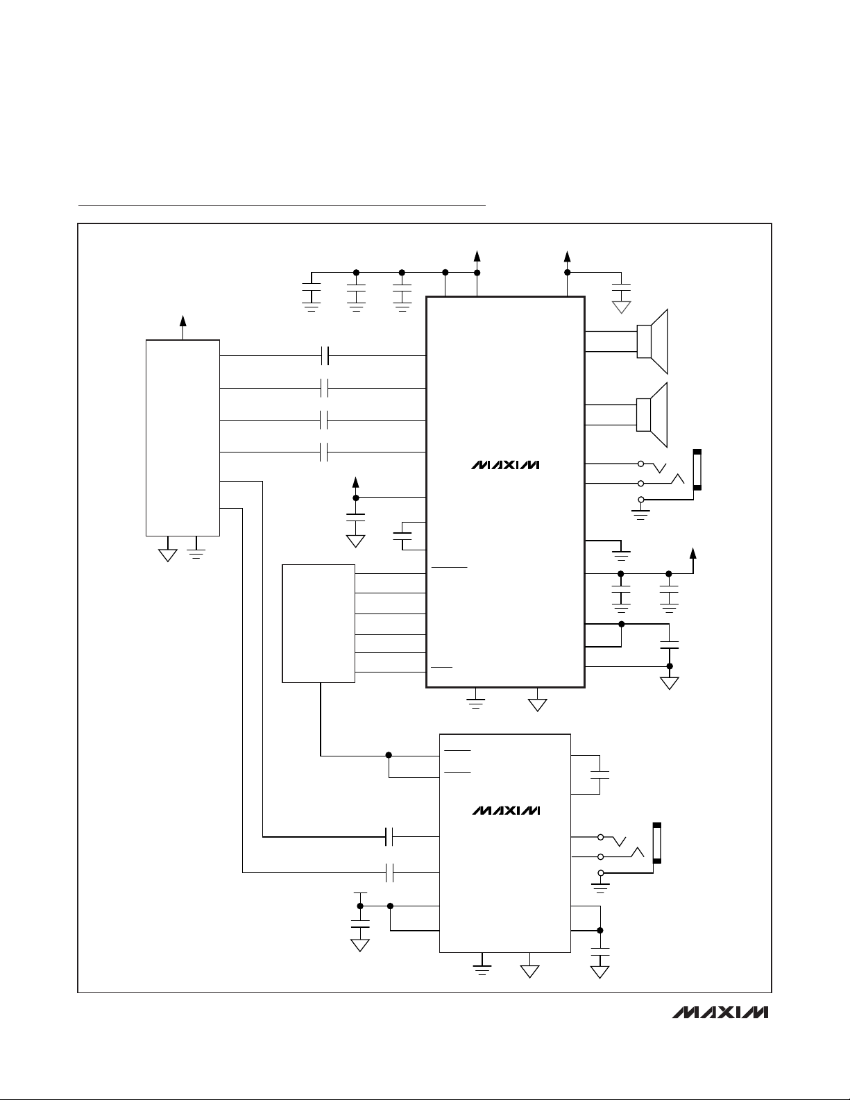
System Diagrams
V
LDO_OUT
SPKR_L
SPKR_R
HDA
CODEC
HP_R
HP_L
MONO
DGND AGND
0.1μF
μ
C
1μF 1μF
C
IN
1μF
C
IN
1μF
C
IN
1μF
C
IN
1μF
5.0V
C
3
1μF
1μF
1μF
5.0V
V
PV
DD
BIAS
SPKR_INL
SPKR_INR
HP_INR
HP_INL
DD
MAX9789
CPV
DD
C
1
C1P
C1N
SPKR_EN
HP_EN
LDO_EN
GAIN1
GAIN2
MUTE
GND
C
BULK
PGND
5.0V
HPV
OUTL+
OUTL-
OUTR+
OUTR-
HPL
HPR
LDO_SET
LDO_OUT
CPV
PV
CPGND
10μF
DD
Ω
4
Ω
4
4.75V
12V
1μF
C
1μF
2
1μF
SS
SS
100μF
0.47μF
0.47μF
0.47μF
1μF
0.01μF
FS2
FS1
G1
G2
SHDN
IN+
IN-
SS
REG
PGND
V
DD
MAX9713
AGND
OUT+
OUT-
C1P
C1N
CHOLD
Ω
8
0.1μF
V
DD
1μF
Page 24
MAX9789/MAX9790
Windows Vista-Compliant, Stereo Class AB Speaker
Amplifiers and DirectDrive Headphone Amplifiers
24 ______________________________________________________________________________________
System Diagrams (continued)
1μF
V
LDO_OUT
1μF
SPKR_L
1μF
SPKR_R
HDA
CODEC
HP1_R
HP1_L
HP2_R
HP2_L
AGNDDGND
1μF
1μF
μC
1μF 0.1μF
+3.3V
C
3
1μF
1μF
+5V
V
PV
DD
DD
SPKR_INL
SPKR_INR
HP_INR
HP_INL
MAX9789
CPV
DD
C
1
C1P
C1N
SPKR_EN
HP_EN
LDO_EN
GAIN2
GAIN1
MUTE
GND
PGND
+3.3V
HPV
OUTL+
OUTL-
OUTR+
OUTR-
HPL
HPR
LDO_SET
LDO_OUT
CP
VSS
P
VSS
CPGND
10μF
DD
HP1
4.75V
1μF 1μF
C
2
1μF
PGND
C1P
C1N
OUTL
OUTR
PV
SV
1μF
HP2
SS
SS
1μF
1μF
+3.3V
1μF
1μF
SHDNR
SHDNL
INR
INL
PV
DD
SV
DD
MAX4411
SGND
Page 25

MAX9789/MAX9790
Windows Vista-Compliant, Stereo Class AB Speaker
Amplifiers and DirectDrive Headphone Amplifiers
______________________________________________________________________________________ 25
Simplified Block Diagrams
(continued)
Chip Information
PROCESS: BiCMOS
Pin Configurations
TOP VIEW
MUTE
HP_INR
HP_INL
GND
LDO_OUT
V
DD
GAIN1
GAIN2
*EP = EXPOSED PADDLE
SPKR_EN
BIAS
2324 22 20 19 18
25
26
27
28
29
30
31
+
32
12
LDO_SET
SPKR_INR
PGND
OUTR+
HP_EN
21
MAX9789
4567
3
PGND
LDO_EN
SPKR_INL
TQFN
OUTR-
EP*
OUTL+
DD
PV
OUTL-
OUTR-
EP*
DD
PV
OUTL-
DD
HPV
17
16
HPL
HPR
15
14
PV
SS
CPV
13
SS
12
C1N
CPGND
11
10
C1P
9
CPV
DD
8
DD
PV
DD
SPKR_EN
PGND
HPV
17
16
HPL
HPR
15
14
PV
SS
CPV
13
SS
12
C1N
CPGND
11
10
C1P
9
CPV
DD
8
DD
PV
MUTE
HP_INR
HP_INL
GND
N.C.
V
GAIN1
GAIN2
DD
BIAS
2324 22 20 19 18
25
26
27
28
29
30
31
+
32
12
N.C.
SPKR_INR
3
OUTR+
HP_EN
21
MAX9790
4567
GND
PGND
SPKR_INL
OUTL+
TQFN
*EP = EXPOSED PADDLE
SPKR_INR
SPKR_INL
HP_INR
HP_INL
SPEAKER SUPPLY
4.5V TO 5.5V
MAX9790
SPKR_EN
HP_EN
MUTE
GAIN1
GAIN2
HEADPHONE SUPPLY
3.0V TO 5.5V
Page 26

MAX9789/MAX9790
Windows Vista-Compliant, Stereo Class AB Speaker
Amplifiers and DirectDrive Headphone Amplifiers
26 ______________________________________________________________________________________
PACKAGE TYPE PACKAGE CODE DOCUMENT NO.
32 TQFN-EP T3255N-1
21-0140
Package Information
For the latest package outline information and land patterns, go to www.maxim-ic.com/packages. Note that a “+”, “#”, or “-” in the
package code indicates RoHS status only. Package drawings may show a different suffix character, but the drawing pertains to the
package regardless of RoHS status.
QFN THIN.EPS
Page 27

MAX9789/MAX9790
Windows Vista-Compliant, Stereo Class AB Speaker
Amplifiers and DirectDrive Headphone Amplifiers
______________________________________________________________________________________ 27
Package Information (continued)
For the latest package outline information and land patterns, go to www.maxim-ic.com/packages. Note that a “+”, “#”, or “-” in the
package code indicates RoHS status only. Package drawings may show a different suffix character, but the drawing pertains to the
package regardless of RoHS status.
Page 28
MAX9789/MAX9790
Windows Vista-Compliant, Stereo Class AB Speaker
Amplifiers and DirectDrive Headphone Amplifiers
Maxim cannot assume responsibility for use of any circuitry other than circuitry entirely embodied in a Maxim product. No circuit patent licenses are
implied. Maxim reserves the right to change the circuitry and specifications without notice at any time.
28
____________________Maxim Integrated Products, 120 San Gabriel Drive, Sunnyvale, CA 94086 408-737-7600
© 2009 Maxim Integrated Products Maxim is a registered trademark of Maxim Integrated Products, Inc.
Revision History
REVISION
NUMBER
2 8/08 Added MAX9789C to data sheet and made miscellaneous clarifications 1–11, 13, 14, 18
3 9/09 Corrected the Block Diagrams 21
REVISION
DATE
DESCRIPTION
PAGES
CHANGED
 Loading...