

Page 1
General Description
The MAX9788 features a mono Class G power amplifier
with an integrated inverting charge-pump power supply
specifically designed to drive the high capacitance of a
ceramic loudspeaker. The charge pump can supply
greater than 700mA of peak output current at 5.5VDC,
guaranteeing an output of 14V
P-P
.
The MAX9788 maximizes battery life by offering highperformance efficiency. Maxim’s proprietary Class G
output stage provides efficiency levels greater than
Class AB devices without the EMI penalties commonly
associated with Class D amplifiers.
The MAX9788 is ideally suited to deliver the high output-voltage swing required to drive ceramic/piezoelectric speakers.
The device utilizes fully differential inputs and outputs,
comprehensive click-and-pop suppression, shutdown
control, and soft-start circuitry. The MAX9788 is fully specified over the -40°C to +85°C extended temperature range
and is available in small lead-free 28-pin TQFN (4mm x
4mm) or 20-bump WLP (2mm x 2.5mm) packages.
Features
♦ Integrated Charge-Pump Power Supply—No
Inductor Required
♦ 14V
P-P
Voltage Swing into Piezoelectric Speaker
♦ 2.7V to 5.5V Single-Supply Operation
♦ Clickless/Popless Operation
♦ Small Thermally Efficient Packages
4mm x 4mm 28-Pin TQFN
2mm x 2.5mm 20-Bump WLP
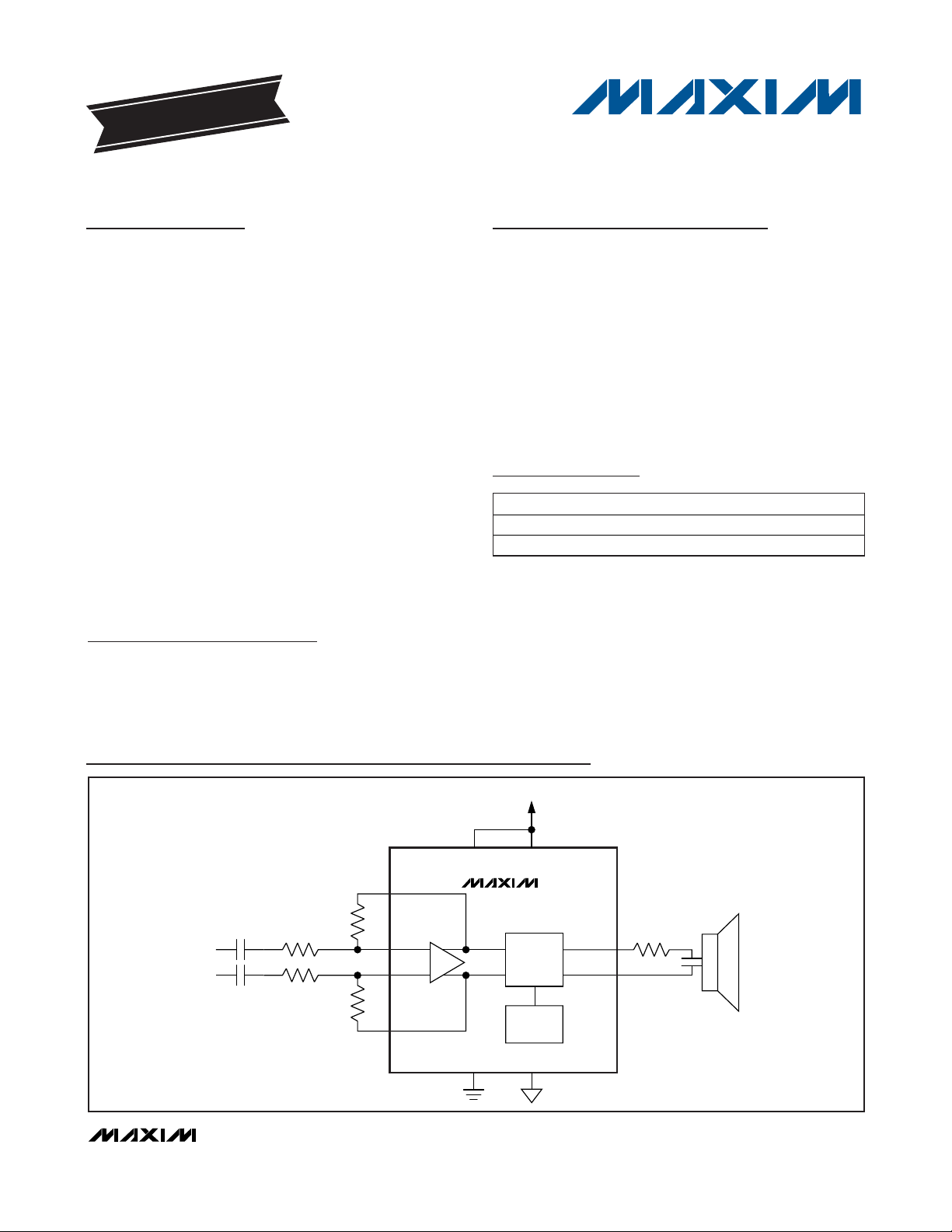
MAX9788
14V
P-P
, Class G Ceramic Speaker Driver
________________________________________________________________
Maxim Integrated Products
1
Ordering Information
MAX9788
+
IN+
FB+
R
IN+
CPV
DD
2.7V TO 5.5V
R
IN-
C
IN
C
IN
IN-
FB-
OUT+
OUT-
-
CLASS G
OUTPUT
STAGE
CHARGE
PUMP
R
FB+
R
FB-
V
CC
CPGNDGND
Simplified Block Diagram
19-0710; Rev 3; 5/08
For pricing, delivery, and ordering information, please contact Maxim Direct at 1-888-629-4642,
or visit Maxim’s website at www.maxim-ic.com.
Typical Application Circuit/Functional Diagram and Pin
Configurations appear at end of data sheet.
EVALUATION KIT
AVAILABLE
Cell Phones
Smartphones
MP3 Players
Personal Media Players
Handheld Gaming
Consoles
Notebook Computers
Applications
+
Denotes a lead-free package.
T = Tape and reel.
G45 indicates protective die coating.
*
EP = Exposed pad.
PART PIN-PACKAGE TEMP RANGE
MAX9788EWP+TG45 20 WLP -40°C to +85°C
MAX9788ETI+ 28 TQFN-EP* -40°C to +85°C
Page 2
MAX9788
14V
P-P
, Class G Ceramic Speaker Driver
2 _______________________________________________________________________________________
ABSOLUTE MAXIMUM RATINGS
ELECTRICAL CHARACTERISTICS
(VCC= V
CPVDD
= V
SHDN
= 3.6V, V
GND
= V
CPGND
= 0V, R
IN+
= R
IN-
= 10kΩ, R
FB+
= R
FB-
= 10kΩ, RFS= 100kΩ, C1 = 4.7µF, C2 =
10µF; load connected between OUT+ and OUT-, Z
LOAD
= 10Ω + 1µF, unless otherwise stated; TA= T
MIN
to T
MAX
, unless otherwise
noted. Typical values are at T
A
= +25°C.) (Notes 2, 3)
Stresses beyond those listed under “Absolute Maximum Ratings” may cause permanent damage to the device. These are stress ratings only, and functional
operation of the device at these or any other conditions beyond those indicated in the operational sections of the specifications is not implied. Exposure to
absolute maximum rating conditions for extended periods may affect device reliability.
(Voltages with respect to GND.)
V
CC
, CPVDD.............................................................-0.3V to +6V
PV
SS
, SVSS...............................................................-6V to +0.3V
CPGND..................................................................-0.3V to +0.3V
OUT+, OUT-...................................(SV
SS
- 0.3V) to (VCC+ 0.3V)
IN+, IN-, FB+, FB- ......................................-0.3V to (V
CC
+ 0.3V)
C1N .........................................(PV
SS
- 0.3V) to (CPGND + 0.3V)
C1P ......................................(CPGND - 0.3V) to (CPV
DD
+ 0.3V)
FS, SHDN ...................................................-0.3V to (V
CC
+ 0.3V)
Continuous Current Into/Out of
OUT+, OUT-, V
CC
, GND, SVSS.....................................800mA
CPV
DD
, CPGND, C1P, C1N, PVSS.................................800mA
Any Other Pin ..................................................................20mA
Continuous Power Dissipation (T
A
= +70°C)
20-Bump WLP (derate 10.3mW/°C
above +70°C) (Note 1)..................................................827mW
28-Pin TQFN (derate 20.8mW/°C above +70°C) ........1667mW
Operating Temperature Range ...........................-40°C to +85°C
Storage Temperature Range .............................-65°C to +150°C
Lead Temperature (soldering, 10s) ................................+300°C
Bump Temperature (soldering) Reflow............................+235°C
Note 1: Package thermal resistances were obtained using the method described in JEDEC specification JESD51-7, using a four-
layer board. For detailed information on package thermal considerations, see www.maxim-ic.com/thermal-tutorial
.
GENERAL
Supply Voltage Range V
Quiescent Current I
Shutdown Current I
Turn-On Time t
Input DC Bias Voltage V
PARAMETER SYMBOL CONDITIONS MIN TYP MAX UNITS
SHDN
CC
CC
ON
BIAS
Inferred from PSRR test 2.7 5.5 V
SHDN = GND 0.3 5 µA
Time from shutdown or power-on to full
operation
IN_ inputs (Note 4) 1.1 1.24 1.4 V
812mA
50 ms
I
= 0mA (slow mode) 55 83 110
Charge-Pump Oscillator
Frequency
SHDN Input Threshold
(Note 5)
SHDN Input Leakage Current ±1 µA
SPEAKER AMPLIFIER
Output Offset Voltage V
Click-and-Pop Level V
Voltage Gain A
Output Voltage V
f
OSC
OS
CP
OUT
LOAD
I
> 100mA (normal mode) 230 330 470
LOAD
V
IH
V
IL
TA = +25°C ±3 ±15
T
≤ TA ≤ T
MIN
Peak voltage into/out of shutdown
A-weighted, 32 samples per second
(Notes 6, 7)
(Notes 4, 8) 11.5 12 12.5 dB
V
f = 1kHz, 1% THD+N
MAX
VCC = 5V 7.1
VCC = 4.2V 5.9
VCC = 3.6V 5.1
= 3.0V 4.2
V
CC
1.4
-67 dBV
0.4
±20
kHz
V
V
mV
RMS
Page 3
MAX9788
14V
P-P
, Class G Ceramic Speaker Driver
_______________________________________________________________________________________ 3
Note 2: All devices are 100% production tested at room temperature. All temperature limits are guaranteed by design.
Note 3: Testing performed with resistive and capacitive loads to simulate an actual ceramic/piezoelectric speaker load,
Z
L
= 1µF + 10Ω.
Note 4: Input DC bias voltage determines the maximum voltage swing of the input signal. Inputing a signal with a peak voltage
of greater than the input DC bias voltage results in clipping.
Note 5: 1.8V logic compatible.
Note 6: Amplifier/inputs AC-coupled to GND.
Note 7: Testing performed at room temperature with 10Ω resistive load in series with 1µF capacitive load connected across the BTL
output for speaker amplifier. Mode transitions are controlled by SHDN. V
CP
is the peak output transient expressed in dBV.
Note 8: Voltage gain is defined as: [V
OUT+
- V
OUT-
] / [V
IN+
- V
IN-
].
Note 9: PV
SS
is forced to -3.6V to simulate boosted rail.
Note 10: Dynamic range is calculated by measuring the RMS voltage difference between a -60dBFS output signal and the noise
floor, then adding 60dB. Full scale is defined as the output signal needed to achieve 1% THD+N.
R
IN_
and R
FB_
have 0.5% tolerance. The Class G output stage has 12dB of gain. Any gain or attenuation at the input
stage will add to or subtract from the gain of the Class G output.
ELECTRICAL CHARACTERISTICS (continued)
(VCC= V
CPVDD
= V
SHDN
= 3.6V, V
GND
= V
CPGND
= 0V, R
IN+
= R
IN-
= 10kΩ, R
FB+
= R
FB-
= 10kΩ, RFS= 100kΩ, C1 = 4.7µF, C2 =
10µF; load connected between OUT+ and OUT-, Z
LOAD
= 10Ω + 1µF, unless otherwise stated; TA= T
MIN
to T
MAX
, unless otherwise
noted. Typical values are at T
A
= +25°C.) (Notes 2, 3)
Output Voltage V
Continuous Output Power P
Power-Supply Rejection Ratio
(Note 4)
Total Harmonic Distortion Plus
Noise
Signal-to-Noise Ratio SNR V
Common-Mode Rejection Ratio CMRR fIN = 1kHz (Note 9) 68 dB
Dynamic Range DR A-weighted (Note 10)
PARAMETER SYMBOL CONDITIONS MIN TYP MAX UNITS
PSRR
THD+N
OUT
OUT
f = 10kHz, 1% THD+N,
= 1µF + 10Ω, no load
Z
L
1% THD+N, f = 1kHz,
= 8Ω
R
L
VCC = 2.7V to 5.5V 63 77
f = 217Hz, 200mV
f = 1kHz, 200mV
f = 20kHz, 200mV
ZL = 1µF + 10Ω, V
= 1µF + 10Ω, V
Z
L
OUT
VCC = 5V 6.5
VCC = 4.2V 5.4
VCC = 3.6V 4.7
V
= 3.0V 3.3
CC
VCC = 5V 2.4
VCC = 4.2V 1.67
VCC = 3.6V 1.25
= 3.0V 0.8
V
CC
ripple 77
P-P
ripple 77
P-P
ripple 58
P-P
= 1kHz / 1.9V
= 5.1V
OUT
= 1kHz / 4.0V
OUT
, A-weighted 108 dB
RMS
VCC = 5V 106
V
RMS
RMS
= 3.6V 105
CC
0.002
0.08
V
RMS
W
dB
%
dB
Page 4
MAX9788
14V
P-P
, Class G Ceramic Speaker Driver
4 _______________________________________________________________________________________
Typical Operating Characteristics
(VCC= V
CPVDD
= V
SHDN
= 3.6V, V
GND
= V
CPGND
= 0V, R
IN+
= R
IN-
= 10kΩ, R
FB+
= R
FB-
= 10kΩ, RFS= 100kΩ, C1 = 4.7µF, C2 =
10µF, Z
L
= 1µF + 10Ω; load terminated between OUT+ and OUT-, unless otherwise stated; TA= T
MIN
to T
MAX
, unless otherwise noted.
Typical values are at T
A
= +25°C.) (Notes 1, 2)
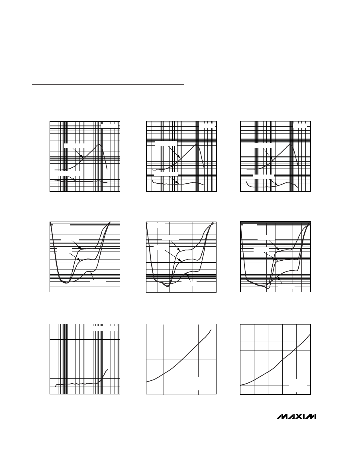
TOTAL HARMONIC DISTORTION PLUS
NOISE vs. FREQUENCY
MAX9788 toc01
FREQUENCY (Hz)
THD+N (%)
10k1k100
0.01
0.1
1
10
0.001
10 100k
V
CC
= 2.7V
V
OUT
= 3V
RMS
V
OUT
= 1.25V
RMS
TOTAL HARMONIC DISTORTION PLUS
NOISE vs. FREQUENCY
MAX9788 toc02
FREQUENCY (Hz)
THD+N (%)
10k1k100
0.01
0.1
1
10
0.001
10 100k
V
CC
= 3.6V
V
OUT
= 1.9V
RMS
V
OUT
= 4V
RMS
TOTAL HARMONIC DISTORTION PLUS
NOISE vs. FREQUENCY
MAX9788 toc03
FREQUENCY (Hz)
THD+N (%)
10k1k100
0.01
0.1
1
10
0.001
10 100k
V
CC
= 5V
V
OUT
= 3V
RMS
V
OUT
= 5.9V
RMS
TOTAL HARMONIC DISTORTION PLUS
NOISE vs. OUTPUT VOLTAGE
MAX9788 toc04
OUTPUT VOLTAGE (V
RMS
)
THD+N (%)
3421
0.01
0.1
1
10
0.001
05
V
CC
= 2.7V
f
IN
= 10kHz
f
IN
= 1kHz
f
IN
= 20Hz
TOTAL HARMONIC DISTORTION PLUS
NOISE vs. OUTPUT VOLTAGE
MAX9788 toc05
OUTPUT VOLTAGE (V
RMS
)
THD+N (%)
53
4
1
2
0.01
0.1
1
10
0.001
06
V
CC
= 3.6V
f
IN
= 10kHz
f
IN
= 1kHz
f
IN
= 20Hz
TOTAL HARMONIC DISTORTION PLUS
NOISE vs. OUTPUT VOLTAGE
MAX9788 toc06
OUTPUT VOLTAGE (V
RMS)
THD+N (%)
7
6
5
4
231
0.01
0.1
1
10
0.001
08
f
IN
= 20Hz
f
IN
= 10kHz
f
IN
= 1kHz
V
CC
= 5V
POWER-SUPPLY REJECTION RATIO
vs. FREQUENCY
MAX9788 toc07
FREQUENCY (Hz)
PSRR (dB)
10k1k100
-80
-70
-60
-50
-40
-30
-20
-10
0
-90
10 100k
V
RIPPLE
= 200mV
P-P
POWER CONSUMPTION
vs. OUTPUT VOLTAGE
MAX9788 toc08
OUTPUT VOLTAGE (V
RMS
)
POWER CONSUMPTION (mW)
3
2
1
25
50
75
100
0
04
V
CC
= 2.7V
f
IN
= 1kHz
1% THD+N
POWER CONSUMPTION
vs. OUTPUT VOLTAGE
MAX9788 toc09
OUTPUT VOLTAGE (V
RMS
)
4
31 2
25
50
75
100
150
125
175
200
0
05
V
CC
= 3.6V
f
IN
= 1kHz
1% THD+N
POWER CONSUMPTION (mW)
Page 5

MAX9788
14V
P-P
, Class G Ceramic Speaker Driver
_______________________________________________________________________________________
5
Typical Operating Characteristics (continued)
(VCC= V
CPVDD
= V
SHDN
= 3.6V, V
GND
= V
CPGND
= 0V, R
IN+
= R
IN-
= 10kΩ, R
FB+
= R
FB-
= 10kΩ, RFS= 100kΩ, C1 = 4.7µF, C2 =
10µF, Z
L
= 1µF + 10Ω; load terminated between OUT+ and OUT-, unless otherwise stated; TA= T
MIN
to T
MAX
, unless otherwise noted.
Typical values are at T
A
= +25°C.) (Notes 1, 2)
SHUTDOWN CURRENT
vs. SUPPLY VOLTAGE
MAX9788 toc15
SUPPLY VOLTAGE (V)
SHUTDOWN CURRENT (μA)
5.55.04.0 4.53.53.0
0.1
0.2
0.3
0.4
0.5
0.6
0.7
0.8
0.9
1.0
0
2.5 6.0
SUPPLY CURRENT
vs. OUTPUT VOLTAGE
MAX9788 toc16
OUTPUT VOLTAGE (V
RMS
)
SUPPLY CURRENT (mA)
6
4
5
3
2
107
10
20
30
40
50
60
70
0
V
CC
= 5V
f
IN
= 1kHz
CLASS G OUTPUT WAVEFORM
MAX9788 toc13
200μs/div
OUT+ - OUT-
10V/div
OUT-
5V/div
OUT+
5V/div
1% THD+N
SUPPLY CURRENT
vs. SUPPLY VOLTAGE
MAX9788 toc14
SUPPLY VOLTAGE (V)
SUPPLY CURRENT (mA)
5.55.04.0 4.53.53.0
4
6
8
2
10
12
0
2.5 6.0
POWER CONSUMPTION
vs. OUTPUT VOLTAGE
350
300
250
200
150
100
POWER CONSUMPTION (mW)
50
0
07
OUTPUT VOLTAGE (V
V
CC
f
IN
1% THD+N
)
RMS
= 5V
= 1kHz
MAX9788 toc10
654321
OUT+ - OUT-
500mV/div
SHDN
5V/div
STARTUP WAVEFORM
10ms/div
MAX9788 toc11
SHUTDOWN WAVEFORM
SHDN
5V/div
OUT+ - OUT-
500mV/div
10ms/div
MAX9788 toc12
Page 6

MAX9788
14V
P-P
, Class G Ceramic Speaker Driver
6 _______________________________________________________________________________________
Pin Description
Typical Operating Characteristics (continued)
(VCC= V
CPVDD
= V
SHDN
= 3.6V, V
GND
= V
CPGND
= 0V, R
IN+
= R
IN-
= 10kΩ, R
FB+
= R
FB-
= 10kΩ, RFS= 100kΩ, C1 = 4.7µF, C2 =
10µF, Z
L
= 1µF + 10Ω; load terminated between OUT+ and OUT-, unless otherwise stated; TA= T
MIN
to T
MAX
, unless otherwise noted.
Typical values are at T
A
= +25°C.) (Notes 1, 2)
OUTPUT AMPLITUDE
vs. FREQUENCY
8
7
)
RMS
OUTPUT AMPLITUDE (V
V
= 3.6V
CC
6
5
4
3
V
= 2.7V
CC
2
1
0
10 100k
FREQUENCY (Hz)
PIN
TQFN WLP
1B2SHDN Shutdown
2, 5, 6, 8, 11, 17,
19, 23, 25, 28
3 A2 C1P
4 A3 CPV
7 A4 FB- Negative Amplifier Feedback
9 A5 IN- Negative Amplifier Input
10 B5 IN+ Positive Amplifier Input
12 B4 FB+ Positive Amplifier Feedback
13 C5 FS
14, 22 D1, D5 V
15, 21 C2, C4 SV
16 D4 OUT- Negative Amplifier Output
18 D3 GND Ground
20 D2 OUT+ Positive Amplifier Output
24 C1 PV
26 B1 C1N
27 A1 CPGND Charge-Pump Ground. Connect to GND.
EP — EP Exposed Pad. Connect the TQFN EP to GND.
V
= 5V
CC
10k1k100
— N.C. No Connection. No internal connection.
MAX9788 toc17
20
18
16
14
12
10
GAIN (dB)
8
6
4
2
0
10 100k
FREQUENCY RESPONSE
FREQUENCY (Hz)
WLP PACKAGE THERMAL DISSIPATION
AND OUTPUT POWER vs. TEMPERATURE
V
= 2V
RMS
OUT
10k1k100
3.5
3.0
MAX9788 toc18
WLP PACKAGE THERMAL DISSIPATION (W)
OUTPUT POWER
2.5
2.0
1.5
PACKAGE THERMAL
DISSIPATION
1.0
0.5
0
-40 90
TEMPERATURE (°C)
NAME FUNCTION
Charge-Pump Flying Capacitor, Positive Terminal. Connect a 4.7µF
capacitor between C1P and C1N.
DD
CC
SS
SS
Charge-Pump Positive Supply
Charge-Pump Frequency Set. Connect a 100kΩ resistor from FS to
GND to set the charge-pump switching frequency.
Supply Voltage. Bypass with a 10µF capacitor to GND.
Amplifier Negative Power Supply. Connect to PVSS.
Charge-Pump Output. Connect a 10µF capacitor between PVSS and
CPGND.
Charge-Pump Flying Capacitor, Negative Terminal. Connect a 4.7µF
capacitor between C1N and C1P.
MAX9788 toc19
VCC = 5V
80706050403020100-10-20-30
3.5
3.0
2.5
2.0
1.5
1.0
0.5
0
OUTPUT POWER (W)
Page 7

MAX9788
14V
P-P
, Class G Ceramic Speaker Driver
_______________________________________________________________________________________ 7
Detailed Description
The MAX9788 Class G power amplifier with inverting
charge pump is the latest in linear amplifier technology.
The Class G output stage offers improved performance
over a Class AB amplifier while increasing efficiency to
extend battery life. The integrated inverting charge
pump generates a negative supply capable of delivering greater than 700mA.
The Class G output stage and the inverting charge
pump allow the MAX9788 to deliver a 14V
P-P
voltage
swing, up to two times greater than a traditional singlesupply linear amplifier.
Class G Operation
The MAX9788 Class G amplifier is a linear amplifier that
operates within a low (V
CC
to GND) and high (VCCto
SV
SS
) supply range. Figure 1 illustrates the transition
from the low to high supply range. For small signals,
the device operates within the lower (VCCto GND) supply range. In this range, the operation of the device
is identical to a traditional single-supply Class AB
amplifier where:
I
LOAD
= I
N1
As the output signal increases so a wider supply is needed, the device begins its transition to the higher supply
range (VCCto SVSS) for the large signals. To ensure a
seamless transition between the low and high supply
ranges, both of the lower transistors are on so that:
I
LOAD
= I
N1
+ I
N2
As the output signal continues to increase, the transition to the high supply is complete. The device then
operates in the higher supply range, where the operation of the device is identical to a traditional dual-supply Class AB amplifier where:
I
LOAD
= I
N2
During operation, the output common-mode voltage of
the MAX9788 adjusts dynamically as the device transitions between supply ranges.
Utilizing a Class G output stage with an inverting
charge pump allows the MAX9788 to realize a 20V
P-P
output swing with a 5V supply.
ON
I
N1
I
N1
P
N1
N2
I
P
ON
OFF
Z
L
V
CC
SV
SS
LOW SUPPLY RANGE OPERATION
I
P
= I
N1
ON
I
N2
I
N2
P
N1
N2
I
P
ON
ON
Z
L
V
CC
BTL CLASS G SUPPLY TRANSITION
SV
SS
SUPPLY TRANSITION
I
P
= IN1 + I
N2
ON P
N1
N2
I
P
OFF
ON
Z
L
V
CC
SV
SS
HIGH SUPPLY RANGE OPERATION
I
P
= I
N2
Figure 1. Class G Supply Transition
Page 8

MAX9788
14V
P-P
, Class G Ceramic Speaker Driver
8 _______________________________________________________________________________________
Inverting Charge Pump
The MAX9788 features an integrated charge pump with an
inverted supply rail that can supply greater than 700mA
over the positive 2.7V to 5.5V supply range. In the case of
the MAX9788, the charge pump generates the negative
supply rail (PV
SS
) needed to create the higher supply
range, which allows the output of the device to operate
over a greater dynamic range as the battery supply collapses over time.
Shutdown Mode
The MAX9788 has a shutdown mode that reduces
power consumption and extends battery life. Driving
SHDN low places the MAX9788 in a low-power (0.3µA)
shutdown mode. Connect SHDN to VCCfor normal
operation.
Click-and-Pop Suppression
The MAX9788 Class G amplifier features Maxim’s comprehensive, industry-leading click-and-pop suppression. During startup, the click-and-pop suppression
circuitry eliminates any audible transient sources internal to the device.
Applications Information
Differential Input Amplifier
The MAX9788 features a differential input configuration,
making the device compatible with many CODECs, and
offering improved noise immunity over a single-ended
input amplifier. In devices such as PCs, noisy digital
signals can be picked up by the amplifier’s input
traces. The signals appear at the amplifier’s inputs as
common-mode noise. A differential input amplifier
amplifies the difference of the two inputs and signals
common to both inputs are canceled out. When configured for differential inputs, the voltage gain of the
MAX9788 is set by:
where A
V
is the desired voltage gain in dB. R
IN+
should
be equal to R
IN-
, and R
FB+
should be equal to R
FB-
.
The Class G output stage has a fixed gain of 4V/V
(12dB). Any gain or attenuation set by the external
input stage resistors will add to or subtract from this
fixed gain. See Figure 2.
In differential input configurations, the common-mode
rejection ratio (CMRR) is primarily limited by the external resistor and capacitor matching. Ideally, to achieve
the highest possible CMRR, the following external components should be selected where:
and
Figure 2. Gain Setting
⎡
A
=×
V
⎢
20 4log
⎢
⎣
⎛
⎜
⎝
⎤
⎞
R
FB
_
⎥
dB
()
⎟
R
⎥
⎠
IN
_
⎦
R
R
FB
IN
R
FB
+
+
−
=
R
IN
−
CC
=
C
IN+
R
IN+
R
C
IN-
IN-
IN IN+
R
FB+
R
FB-
FB+
IN+
IN-
FB-
−
MAX9788
+
-
CLASS G
OUTPUT
STAGE
Page 9

Driving a Ceramic Speaker
Applications that require thin cases, such as today’s
mobile phones, demand that external components
have a small form factor. Dynamic loudspeakers that
use a cone and voice coil typically cannot conform to
the height requirements. The option for these applications is to use a ceramic/piezoelectric loudspeaker.
Ceramic speakers are much more capacitive than a conventional loudspeaker. Typical capacitance values for
such a speaker can be greater than 1µF. High peak-topeak voltage drive is required to achieve acceptable
sound pressure levels. The high output voltage requirement coupled with the capacitive nature of the speaker
demand that the amplifier supply much more current at
high frequencies than at lower frequencies. Above 10kHz,
the typical speaker impedance can be less than 16Ω.
The MAX9788 is ideal for driving a capacitive ceramic
speaker. The high charge-pump current limit allows for a
flat frequency response out to 20kHz while maintaining
high output voltage swings. See the Frequency Response
graph in the
Typical Operating Characteristics
. Figure 3
shows a typical circuit for driving a ceramic speaker.
A 10Ω series resistance is recommended between the
amplifier output and the ceramic speaker load to ensure
the output of the amplifier sees some fixed resistance at
high frequencies when the speaker is essentially an
electrical short.
Component Selection
Input-Coupling Capacitor
The AC-coupling capacitors (C
IN_
) and input resistors
(R
IN_
) form highpass filters that remove any DC bias
from an input signal (see the
Functional Diagram/
Typical Operating Circuit
). C
IN_
blocks DC voltages
from the amplifier input. The -3dB point of the highpass
filter, assuming zero source impedance due to the
input signal source, is given by:
Ceramic speakers generally perform best at frequencies greater than 1kHz. Low frequencies can deflect
the piezoelectric speaker element so that high frequencies cannot be properly reproduced. This can cause
distortion in the speaker’s usable frequency band.
Select a CINso the f
-3dB
closely matches the low frequency response of the ceramic speaker. Use capacitors with low-voltage coefficient dielectrics. Aluminum
electrolytic, tantalum, or film dielectric capacitors are
good choices for AC-coupling capacitors. Capacitors
with high-voltage coefficients, such as ceramics (nonC0G dielectrics), can result in increased distortion at
low frequencies.
Charge-Pump Capacitor Selection
Use capacitors with an ESR less than 50mΩ for optimum performance. Low-ESR ceramic capacitors minimize the output resistance of the charge pump. For
best performance over the extended temperature
range, select capacitors with an X7R dielectric.
Flying Capacitor (C1)
The value of the flying capacitor (C1) affects the load
regulation and output resistance of the charge pump. A
C1 value that is too small degrades the device’s ability
to provide sufficient current drive. Increasing the value
of C1 improves load regulation and reduces the chargepump output resistance to an extent. Above 1µF, the onresistance of the switches and the ESR of C1 and C2
dominate. A 4.7µF capacitor is recommended.
MAX9788
14V
P-P
, Class G Ceramic Speaker Driver
_______________________________________________________________________________________ 9
Figure 3. Driving a Ceramic Speaker
MAX9788
f
dB
−
3
=
RC
××
2π
1
IN IN
__
Hz
()
OUT+
CLASS G
OUTPUT
STAGE
OUT-
R
L
Page 10

MAX9788
Hold Capacitor (C2)
The output capacitor value and ESR directly affect the
ripple at PVSS. Increasing C2 reduces output ripple.
Likewise, decreasing the ESR of C2 reduces both ripple and output resistance. A 10µF capacitor is recommended.
Charge-Pump Frequency Set Resistor (RFS)
The charge pump operates in two modes. When the
charge pump is loaded below 100mA, it operates in a
slow mode where the oscillation frequency is reduced to
1/4 of its normal operating frequency. Once loaded, the
charge-pump oscillation frequency returns to normal
operation. In applications where the design may be sensitive to the operating charge-pump oscillation frequency, the value of the external resistor RFScan be changed
to adjust the charge-pump oscillation frequency shown
in Figure 4. A 100kΩ resistor is recommended.
Ceramic Speaker Impedance
Characteristics
A 1µF capacitor is a good model for the ceramic
speaker as it best approximates the impedance of a
ceramic speaker over the audio band. When selecting
a capacitor to simulate a ceramic speaker, the voltage
rating or the capacitor must be equal to or higher than
the expected output voltage swing. See Figure 5.
Series Load Resistor
The capacitive nature of the ceramic speaker results in
very low impedances at high frequencies. To prevent
the ceramic speaker from shorting the MAX9788 output
at high frequencies, a series load resistor must be
used. The output load resistor and the ceramic speaker
create a lowpass filter. To set the rolloff frequency of
the output filter, the approximate capacitance of the
speaker must be known. This information can be
obtained from bench testing or from the ceramic
speaker manufacturer. A series load resistor greater
than 10Ω is recommended. Set the lowpass filter cutoff
frequency with the following equation:
WLP Applications Information
For the latest application details on WLP construction,
dimensions, tape carrier information, PCB techniques,
bump-pad layout, and recommended reflow temperature profile, as well as the latest information on reliability
testing results, go to the Maxim website at www.maximic.com/ucsp for the application note,
UCSP—A Wafer-
Level Chip-Scale Package
.
14V
P-P
, Class G Ceramic Speaker Driver
10 ______________________________________________________________________________________
Figure 4. Charge-Pump Oscillation Frequency vs. R
FS
Figure 5. Ceramic Speaker and Capacitor Impedance
f
LP
=
2π
1
RC
××
L SPEAKER
Hz
()
CHARGE-PUMP OSCILLATION
FREQUENCY vs. R
600
550
500
450
400
350
300
250
CHARGE-PUMP OSCILLATION FREQUENCY (kHz)
200
50 150
RFS (kΩ)
I
LOAD
FS
12510075
> 100mA
MAX9788 fig04
1M
100k
10k
IMPEDANCE (Ω)
100
10
IMPEDANCE vs. FREQUENCY
1μF CAPACITOR
1k
CERAMIC
SPEAKER
0.001 100
FREQUENCY (Hz)
MAX9788 fig05
1010.10.01
Page 11

MAX9788
14V
P-P
, Class G Ceramic Speaker Driver
______________________________________________________________________________________ 11
Typical Application Circuit/Functional Diagram
SHDN
CONTROL
SIGNAL
C
IN
0.47μF
C
IN
0.47μF
( ) WLP PACKAGE
DEVICE SHOWN WITH A
*SYSTEM-LEVEL REQUIREMENT TYPICALLY 10μF
R
10kΩ
R
10kΩ
IN+
IN-
= 12dB
V
R
10kΩ
R
10kΩ
FB+
FB-
20kΩ
12 (B4)
10 (B5)
9 (A5)
7 (A4)
18 (D3) 27 (A1) 26 (B1) 3 (A2)
14, 22
(D1, D5)
1 (B2)
V
SHDN
FB+
IN+
IN-
FB-
GND
CC
+
-
CPGND PV
C1N
V
DD
4 (A3)
CPV
DD
MAX9788
CLASS G
OUTPUT
STAGE
CHARGE
PUMP
C1
4.7μF
C1P
0.1μF
SS
24 (C1)
*
OUT+
OUT-
SV
15, 21
(C2, C4)
R
L
20 (D2)
16 (D4)
13 (C5)
FS
SS
C2
10μF
10Ω
R
FS
100kΩ
Page 12

MAX9788
14V
P-P
, Class G Ceramic Speaker Driver
12 ______________________________________________________________________________________
Pin Configurations
Chip Information
PROCESS: BiCMOS
Package Information
For the latest package outline information and land patterns, go
to www.maxim-ic.com/packages
.
PACKAGE TYPE PACKAGE CODE DOCUMENT NO.
20 WLP W202A2+1
21-0059
28 TQFN T2844-1
21-0139
TOP VIEW
+
SHDN
1
2
N.C.
3
C1P
CPV
4
DD
5
N.C.
6
N.C.
FB-
7
*EXPOSED PAD.
N.C.
28
EP*
8
N.C.
CPGND
C1N
27
26
MAX9788
9
10
IN-
IN+
THIN QFN
N.C.
25
11
N.C.
PV
24
12
FB+
TOP VIEW
(BUMP SIDE DOWN)
SS
N.C.
23
13
FS
CC
V
22
SV
21
SS
20
OUT+
19
N.C.
18
GND
17
N.C.
16
OUT-
SV
15
SS
14
CC
V
A
B
C
D
1
CPGND
C1N
PV
SS
V
CC
MAX9788
FB-
FB+
SV
OUT-
4
IN-
IN+
FS
SS
V
CC
23 5
CPV
C1P
SHDN
SV
OUT+
SS
DD
GND
WLP
Page 13

MAX9788
14V
P-P
, Class G Ceramic Speaker Driver
Maxim cannot assume responsibility for use of any circuitry other than circuitry entirely embodied in a Maxim product. No circuit patent licenses are
implied. Maxim reserves the right to change the circuitry and specifications without notice at any time.
Maxim Integrated Products, 120 San Gabriel Drive, Sunnyvale, CA 94086 408-737-7600 ____________________
13
© 2008 Maxim Integrated Products is a registered trademark of Maxim Integrated Products, Inc.
Revision History
REVISION
NUMBER
0 12/06 Initial release —
1 11/07
2 2/08
3 5/08 Updated Typical Application Circuit and corrected stylistic errors 1–6, 11
REVISION
DATE
DESCRIPTION
Include tape and reel note, edit Absolute Maximum Ratings, update TQFN
package outline
Replaced USCP with WLP package throughout data sheet including new
WLP package outline, added new TOC 19 and Note 1
1, 2, 3, 6, 10, 11, 12,
PAGES
CHANGED
1, 2,13, 14
15, 16
 Loading...