

General Description
The MAX9775/MAX9776 combine a high-efficiency
Class D, stereo/mono audio power amplifier with a
mono DirectDrive
®
receiver amplifier and a stereo
DirectDrive headphone amplifier.
Maxim’s 3rd-generation, ultra-low-EMI, Class D audio
power amplifiers provide Class AB performance with
Class D efficiency. The MAX9775/MAX9776 deliver
1.5W per channel into a 4Ω load from a 5V supply and
offer efficiencies up to 79%. Active emissions limiting
circuitry and spread-spectrum modulation greatly
reduce EMI, eliminating the need for output filtering
found in traditional Class D devices.
The MAX9775/MAX9776 utilize a fully differential architecture, a full-bridged output, and comprehensive clickand-pop suppression. A 3D stereo enhancement
function allows the MAX9775 to widen the stereo sound
field immersing the listener in a cleaner, richer sound
experience than typically found in portable applications.
The devices utilize a flexible, user-defined mixer architecture that includes an input mixer, volume control, and
output mixer. All control is done through I2C.
The mono receiver amplifier and stereo headphone
amplifier use Maxim’s DirectDrive architecture that produces a ground-referenced output from a single supply,
eliminating the need for large DC-blocking capacitors,
saving cost, space, and component height.
The MAX9775 is available in a 36-bump WLP (3mm x
3mm) package. The MAX9776 is available in a 32-pin
TQFN (5mm x 5mm) or a 36-bump WLP (3mm x 3mm)
package. Both devices are specified over the extended
-40°C to +85°C temperature range.
Applications
Cell Phones
Portable Multimedia Players
Handheld Gaming Consoles
Features
♦ Unique Spread-Spectrum Modulation and Active
Emissions Limiting Significantly Reduces EMI
♦ 3D Stereo Enhancement (MAX9775 Only)
♦ Up to 3 Stereo Inputs
♦ 1.5W Stereo Speaker Output (4Ω, V
DD
= 5V)
♦ 50mW Mono Receiver/Stereo Headphone Outputs
(32Ω, V
DD
= 3.3V)
♦ High PSRR (68dB at 217Hz)
♦ 79% Efficiency (V
DD
= 3.3V, RL= 8Ω, P
OUT
=
470mW)
♦ I
2
C Control—Input Configuration, Volume Control,
Output Mode
♦ Click-and-Pop Suppression
♦ Low Total Harmonic Distortion (0.03% at 1kHz)
♦ Current-Limit and Thermal Protection
♦ Available in Space-Saving, 36-Bump WLP (3mm x
3mm) and 32-Pin TQFN (5mm x 5mm) Packages
MAX9775/MAX9776
2 x 1.5W, Stereo Class D Audio Subsystem
with DirectDrive Headphone Amplifier
________________________________________________________________
Maxim Integrated Products
1
Ordering Information
MAX9775
MIXER/
MUX
GAIN
CONTROL
3D
SOUND
CONTROL
I2C
INTERFACE
SINGLE SUPPLY 2.7V TO 5.5V
MAX9776
MIXER/
MUX
GAIN
CONTROL
I2C
INTERFACE
SINGLE SUPPLY 2.7V TO 5.5V
Simplified Block Diagrams
19-0746; Rev 4; 8/08
For pricing, delivery, and ordering information, please contact Maxim Direct at 1-888-629-4642,
or visit Maxim’s website at www.maxim-ic.com.
Pin Configurations appear at end of data sheet.
PART PIN-PACKAGE
CLASS D
AMPLIFIER
MAX9775EBX+T 36 WLP* Stereo
MAX9776ETJ+ 32 TQFN-EP** Mono
MAX9776EBX+T 36 WLP* Mono
Note: All devices are specified over the -40°C to +85°C operating temperature range.
+
Denotes a lead-free/RoHS-compliant package.
*
Four center bumps depopulated.
**
EP = Exposed pad.
DirectDrive is a registered trademark of Maxim Integrated
Products, Inc.
MAX9775/MAX9776
2 x 1.5W, Stereo Class D Audio Subsystem
with DirectDrive Headphone Amplifier
2 _______________________________________________________________________________________
ABSOLUTE MAXIMUM RATINGS
ELECTRICAL CHARACTERISTICS
(VDD= PVDD= CPVDD= 3.3V, V
GND
= V
PGND
= V
CPGND
= 0V, SHDN = VDD, I2C settings (INA gain = +20dB, INB gain = INC gain =
0dB, volume setting = 0dB, mono path gain = 0dB, SHDN = 1, SSM = 1). Speaker load resistors (R
LSP
) are terminated between
OUT_+ and OUT_-, headphone load resistors are terminated to GND, unless otherwise noted. C1 = C2 = C3 = 1µF. T
A
= T
MIN
to
T
MAX
, unless otherwise noted. Typical values are at TA= +25°C.) (Note 1)
Stresses beyond those listed under “Absolute Maximum Ratings” may cause permanent damage to the device. These are stress ratings only, and functional
operation of the device at these or any other conditions beyond those indicated in the operational sections of the specifications is not implied. Exposure to
absolute maximum rating conditions for extended periods may affect device reliability.
VDDto GND..............................................................................6V
PV
DD
to PGND .........................................................................6V
CPV
DD
to CPGND ....................................................................6V
CPV
SS
to CPGND .....................................................-6V to +0.3V
V
SS
to CPGND..........................................................-6V to +0.3V
C1N .......................................(CPV
SS
- 0.3V) to (CPGND + 0.3V)
C1P.......................................(CPGND - 0.3V) to (CPV
DD
+ 0.3V)
HPL, HPR to GND...................(CPV
SS
- 0.3V) to (CPVDD+ 0.3V)
GND to PGND and CPGND................................................±0.3V
V
DD
to PVDDand CPVDD....................................................±0.3V
SDA, SCL to GND.....................................................-0.3V to +6V
All other pins to GND..................................-0.3V to (V
DD
+ 0.3V)
Continuous Current In/Out of PV
DD
, PGND, CPVDD, CPGND,
OUT__, HPR, and HPL..................................................±800mA
Continuous Input Current CPV
SS
......................................260mA
Continuous Input Current (all other pins) .........................±20mA
Duration of Short Circuit Between
OUT_+ and OUT_- ..................................................Continuous
Duration of HP_, OUT_ Short Circuit to
GND or PV
DD
..........................................................Continuous
Continuous Power Dissipation (T
A
= +70°C)
36-Bump (3mm x 3mm) UCSP Multilayer Board
(derate 17.0mW/°C above +70°C)...........................1360.5mW
32-Pin (5mm x 5mm) TQFN Single-Layer Board
(derate 21.3mW/°C above +70°C)...........................1702.1mW
32-Pin TQFN Multilayer Board (derate 34.5mW/°C
above +70°C)...........................................................2758.6mW
Junction Temperature......................................................+150°C
Operating Temperature Range ...........................-40°C to +85°C
Storage Temperature Range .............................-65°C to +150°C
Lead Temperature (soldering, 10s) .................................+300°C
GENERAL
Supply Voltage Range
Quiescent Current (Mono) I
Quiescent Current (Stereo) I
Mute Current I
Shutdown Current I
Turn-On Time t
Input Resistance R
Common-Mode Rejection Ratio CMRR TA = +25°C, fIN = 1kHz (Note 2) 45 50 60 dB
Input DC Bias Voltage V
PARAMETER SYMBOL CONDITIONS MIN TYP MAX UNITS
V
DD
C
, P
PVDD
DD
DD
MUTE
SHDN
ON
IN
BIAS
VDD
,
Inferred from PSRR test 2.7 5.5 V
Output mode 1, 6, 11 (Rx mode) 6.3 10
Output mode 4, 9, 14 (HP mode) 8 12.6
Output mode 2, 7, 12 (SP mode) 9.5 15
Output mode 3, 8, 13 (SP and HP mode) 12.9 18
Output mode 1, 6, 11 (Rx mode) 7
Output mode 4, 9, 14 (HP mode) 9
Output mode 2, 7, 12 (SP mode) 16.5
Output mode 3, 8, 13 (SP and HP mode) 20
Current in mute (low power) 4.7 10 mA
Hard shutdown SHDN = GND 0.1 10
Soft shutdown
Time from shutdown or power-on to full
operation
B and C pair inputs, TA = +25°C,
VOL = max
A pair inputs, TA = +25°C, +20dB 3.5 5.5 8.0 kΩ
IN_ inputs 1.12 1.25 1.38 V
See the I
section
2
C Interface
17.5 28 41.0 kΩ
8.5 15
30 ms
mA
mA
µA
MAX9775/MAX9776
2 x 1.5W, Stereo Class D Audio Subsystem
with DirectDrive Headphone Amplifier
_______________________________________________________________________________________ 3
ELECTRICAL CHARACTERISTICS (continued)
(VDD= PVDD= CPVDD= 3.3V, V
GND
= V
PGND
= V
CPGND
= 0V, SHDN = VDD, I2C settings (INA gain = +20dB, INB gain = INC gain =
0dB, volume setting = 0dB, mono path gain = 0dB, SHDN = 1, SSM = 1). Speaker load resistors (R
LSP
) are terminated between
OUT_+ and OUT_-, headphone load resistors are terminated to GND, unless otherwise noted. C1 = C2 = C3 = 1µF. T
A
= T
MIN
to
T
MAX
, unless otherwise noted. Typical values are at TA= +25°C.) (Note 1)
PARAMETER SYMBOL CONDITIONS MIN TYP MAX UNITS
SPEAKER AMPLIFIERS
Output Offset Voltage V
Click-and-Pop Level K
Power-Supply Rejection Ratio
(Note 3)
Current Limit 1.6 A
Total Harmonic Distortion Plus
Noise (Note 4)
Signal-to-Noise Ratio SNR
Output Frequency f
Efficiency η
Gain A
Channel-to-Channel Gain
Tracking (Note 5)
3D Sound Resistors (Note 5) R
Crosstalk (Notes 4, 5)
OS
CP
PSRR T
OUT
THD+N f = 1kHz
OSC
TA = +25°C ±5.5 ±23.5
T
≤ TA ≤ T
MIN
P eak vol tag e,
= + 25°C ,
T
A
A- w ei g hted , 32
sam p l es p er second
( N otes 2, 3)
MAX
Into shutdown -62
Out of shutdown -60
Into mute -63
Out of mute -62
VDD = 2.7V to 5.5V 48 70
f = 217Hz,
P-P
P-P
ripple
ripple
= +25°C
A
100mV
f = 1kHz,
100mV
f = 20kHz,
P-P
ripple
100mV
RL = 4Ω, VDD = 5V 1500
THD+N = 1%,
= +25°C
T
A
RL = 8Ω, VDD = 3.3V 450Output Power (Note 4) P
R
= 8Ω, VDD = 5V 1115
L
RL = 8Ω,
P
= 125mW
OUT
R
= 4Ω,
L
P
= 250mW
OUT
V
= 1.8V
OUT
R
= 8Ω, 3D not
L
active (Note 3)
RMS
,
BW = 20Hz to 20kHz 81
A-weighted 84
Fixed-frequency modulation 1100
Spread-spectrum modulation 1100 ± 30
P
= 470mW, f = 1kHz both channels
OUT
driven, L = 68µH in series with 8Ω load
V
= +25°C ±1 %
T
A
Used with 22nF and 2.2nF external
3D
capacitors
L to R, R to L, f = 10kHz, R
= 300mV
V
OUT
RMS
= 8Ω,
L
579kΩ
±40
68
60
50
0.03
0.04
79 %
12 dB
73 dB
mV
dB
dB
mW
dB
kHz
%
MAX9775/MAX9776
2 x 1.5W, Stereo Class D Audio Subsystem
with DirectDrive Headphone Amplifier
4 _______________________________________________________________________________________
ELECTRICAL CHARACTERISTICS (continued)
(VDD= PVDD= CPVDD= 3.3V, V
GND
= V
PGND
= V
CPGND
= 0V, SHDN = VDD, I2C settings (INA gain = +20dB, INB gain = INC gain =
0dB, volume setting = 0dB, mono path gain = 0dB, SHDN = 1, SSM = 1). Speaker load resistors (R
LSP
) are terminated between
OUT_+ and OUT_-, headphone load resistors are terminated to GND, unless otherwise noted. C1 = C2 = C3 = 1µF. T
A
= T
MIN
to
T
MAX
, unless otherwise noted. Typical values are at TA= +25°C.) (Note 1)
RECEIVER AMPLIFIER
Output Offset Voltage V
Click-and-Pop Level K
Power-Supply Rejection Ratio
(Note 3)
Output Power P
Gain A
Total Harmonic Distortion Plus
Noise
Signal-to-Noise Ratio SNR
Slew Rate SR 0.3 V/µs
Capacitive Drive C
HEADPHONE AMPLIFIERS
Output Offset Voltage V
Click-and-Pop Level K
ESD Protection HP_
Power-Supply Rejection Ratio
(Note 3)
PARAMETER SYMBOL CONDITIONS MIN TYP MAX UNITS
OS
CP
PSRR T
OUT
V
THD+N
L
OS
CP
PSRR T
TA = +25°C ±1.8 ±5.5 mV
Peak voltage, TA =
+25°C, A-weighted,
32 samples per
second (Notes 3, 6)
= +25°C
A
TA = +25°C,
THD+N = 1%
RL = 16Ω (V
= 32Ω (V
R
L
R
= 16Ω, V
L
800mV
TA = +25°C ±1.8 ±5.5 mV
Peak voltage, TA =
+25°C, A-weighted,
32 samples per
second (Notes 2, 4)
= +25°C
A
RMS
OUT
OUT
OUT
(Note 3)
Into shutdown -62
Into mute -67
Out of shutdown -63
Out of mute -66
VDD = 2.7V to 5.5V 58 80
f = 217Hz,
100mV
f = 1kHz,
100mV
f = 20kHz,
100mV
RL = 16Ω 60
R
L
= 800mV
= 800mV
BW = 20Hz to 20kHz 87
=
A-weighted 89
Into shutdown -61
Into mute -65
Out of shutdown -60
Out of mute -64
Contact ±4
Air ±8
VDD = 2.7V to 5.5V 58 80
f = 217Hz,
100mV
f = 1kHz,
100mV
f = 20kHz,
100mV
ripple
P-P
ripple
P-P
ripple
P-P
= 32Ω 50
, f = 1kHz) 0.03
RMS
, f = 1kHz) 0.024
RMS
ripple
P-P
ripple
P-P
ripple
P-P
80
70
62
3dB
300 pF
80
70
62
dB
dB
mW
%
dB
dB
kV
dB
MAX9775/MAX9776
2 x 1.5W, Stereo Class D Audio Subsystem
with DirectDrive Headphone Amplifier
_______________________________________________________________________________________ 5
ELECTRICAL CHARACTERISTICS (continued)
(VDD= PVDD= CPVDD= 3.3V, V
GND
= V
PGND
= V
CPGND
= 0V, SHDN = VDD, I2C settings (INA gain = +20dB, INB gain = INC gain =
0dB, volume setting = 0dB, mono path gain = 0dB, SHDN = 1, SSM = 1). Speaker load resistors (R
LSP
) are terminated between
OUT_+ and OUT_-, headphone load resistors are terminated to GND, unless otherwise noted. C1 = C2 = C3 = 1µF. T
A
= T
MIN
to
T
MAX
, unless otherwise noted. Typical values are at TA= +25°C.) (Note 1)
Output Power P
Current Limit 170 mA
Gain A
Channel-to-Channel Gain
Tracking
Total Harmonic Distortion Plus
Noise
Signal-to-Noise Ratio SNR
Slew Rate SR 0.3 V/µs
Capacitive Drive C
Crosstalk
VOLUME CONTROL
Volume Control
Mono Gain All outputs
Input Pair A Control
Mute Attenuation
(Minimum Volume)
DIGITAL INPUTS (SHDN, SDA, SCL)
Input-Voltage High V
Input-Voltage Low V
Input Hysteresis (SDA, SCL) V
PARAMETER SYMBOL CONDITIONS MIN TYP MAX UNITS
THD+N
OUT
V
L
IH
IL
HYS
TA = +25°C,
THD+N = 1%
T
= +25°C ±1 %
A
RL = 16Ω (V
R
= 32Ω (V
L
R
= 16Ω,
L
V
OUT
L to R, R to L, f = 10kHz, R
V
OUT
IN+6dB = 0
(minimum gain
setting)
IN+6dB = 1
(maximum gain
setting)
INA+20dB = 0 (minimum gain setting) Set by IN+6dB
INA+20dB = 1 (maximum gain setting) 20
V
= 1V
IN
OUT
OUT
= 800mV
= 160mV
RMS
RMS
RMS
RL = 16Ω 60
R
= 32Ω 50
L
= 800mV
= 800mV
, f = 1kHz) 0.03
RMS
, f = 1kHz) 0.024
RMS
BW = 20Hz to
20kHz
A-weighted 93
= 16Ω,
L
HP gain (max) 3
SP gain (max) 12
HP gain (min) -72
SP gain (min) -63
HP gain (max) 9
SP gain (max) 18
HP gain (min) -61
SP gain (min) -57
Mono+6dB = 0 0
Mono+6dB = 1 6
1.4 V
+3 dB
92
300 pF
75 dB
80 dB
200 mV
0.4 V
mW
%
dB
dB
dB
dB
MAX9775/MAX9776
2 x 1.5W, Stereo Class D Audio Subsystem
with DirectDrive Headphone Amplifier
6 _______________________________________________________________________________________
ELECTRICAL CHARACTERISTICS (continued)
(VDD= PVDD= CPVDD= 3.3V, V
GND
= V
PGND
= V
CPGND
= 0V, SHDN = VDD, I2C settings (INA gain = +20dB, INB gain = INC gain =
0dB, volume setting = 0dB, mono path gain = 0dB, SHDN = 1, SSM = 1). Speaker load resistors (R
LSP
) are terminated between
OUT_+ and OUT_-, headphone load resistors are terminated to GND, unless otherwise noted. C1 = C2 = C3 = 1µF. T
A
= T
MIN
to
T
MAX
, unless otherwise noted. Typical values are at TA= +25°C.) (Note 1)
Note 1: All devices are 100% production tested at room temperature. All temperature limits are guaranteed by design.
Note 2: Measured at headphone outputs.
Note 3: Amplifier inputs AC-coupled to GND.
Note 4: Testing performed with a resistive load in series with an inductor to simulate an actual speaker load. For R
L
= 8Ω, L = 68µH;
for R
L
= 4Ω, L = 47µH.
Note 5: MAX9775 only.
Note 6: Testing performed at room temperature with an 8Ω resistive load in series with a 68µH inductive load connected across BTL
outputs for speaker amplifier. Testing performed with a 32Ω resistive load connected between OUT_ and GND for headphone amplifier. Testing performed with 32Ω resistive load connected between OUTRx and GND for mono receiver amplifier. Mode transitions are controlled by I
2
C.
Note 7: Guaranteed by design.
SDA, SCL Input Capacitance C
Input Leakage Current I
Pulse Width of Spike Suppressed t
DIGITAL OUTPUTS (SDA Open Drain)
Output Low Voltage SDA V
Output Fall Time SDA t
I2C INTERFACE TIMING (Note 7)
Serial Clock Frequency f
Bus Free Time Between STOP
and START Conditions
START Condition Hold t
STOP Condition Setup Time t
Clock Low Period t
Clock High Period t
Data Setup Time t
Data Hold Time t
Maximum Receive SCL/SDA Rise
Time
Maximum Receive SCL/SDA Fall
Time
Setup Time for STOP Condition t
Capacitive Load for Each Bus
Line
PARAMETER SYMBOL CONDITIONS MIN TYP MAX UNITS
HD:STA
SU:STA
SU:DAT
HD:DAT
SU:STO
IN
IN
SP
OL
OF
SCL
t
BUF
LOW
HIGH
t
R
t
F
C
b
I
= 6mA 0.4 V
SINK
V
H(MIN)
10pF to 400pF, I
10 pF
0.3 5.0 µA
50 ns
to V
bus capacitance =
L(MAX)
SINK
= 3mA
250 ns
DC 400 kHz
1.3 µs
0.6 µs
0.6 µs
1.3 µs
0.6 µs
100 ns
0 900 ns
0.6 µs
300 ns
300 ns
400 pF
MAX9775/MAX9776
2 x 1.5W, Stereo Class D Audio Subsystem
with DirectDrive Headphone Amplifier
_______________________________________________________________________________________
7
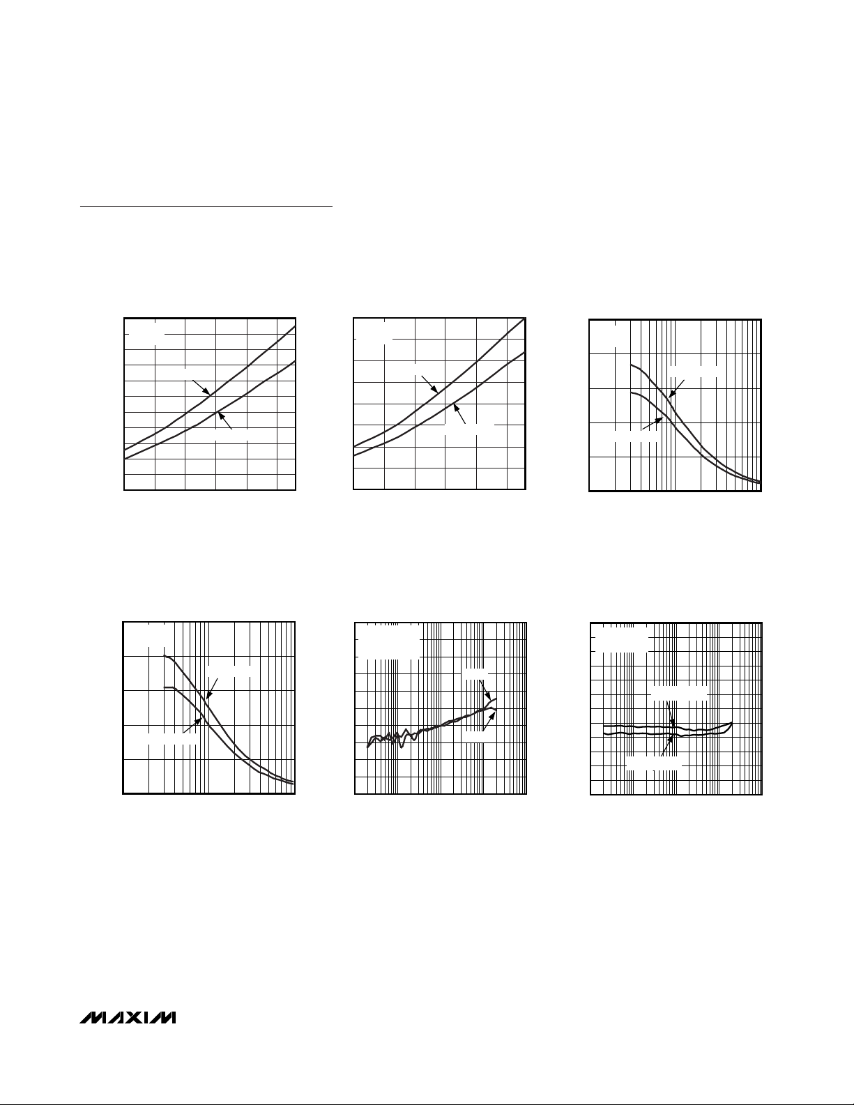
Typical Operating Characteristics
(VDD= PVDD= CPVDD= 3.3V, GND = PGND = CPGND = 0V, SHDN = VDD, I2C default gain settings (INA gain = +20dB, INB gain =
INC gain = 0dB, volume setting = 0dB, mono path gain = 0dB, SHDN = 1, SSM = 1). Speaker load resistors (R
LSP
) are terminated
between OUT_+ and OUT_-, headphone load resistors are terminated to GND, unless otherwise stated. C1 = C2 = C3 = 1µF. T
A
=
+25°C, unless otherwise noted.)
TOTAL HARMONIC DISTORTION PLUS NOISE
vs. FREQUENCY
1
VDD = 5V
= 4Ω
R
L
P
= 400mW
0.1
THD+N (%)
0.01
0.001
OUT
P
= 1000mW
OUT
10 100k
FREQUENCY (Hz)
10k1k100
TOTAL HARMONIC DISTORTION PLUS NOISE
vs. FREQUENCY
1
VDD = 3.3V
= 8Ω
R
L
P
= 300mW
0.1
THD+N (%)
0.01
OUT
P
OUT
= 150mW
MAX9775/76 toc01
MAX9775/76 toc04
TOTAL HARMONIC DISTORTION PLUS NOISE
vs. FREQUENCY
1
VDD = 5V
= 8Ω
R
L
P
= 150mW
OUT
0.1
THD+N (%)
0.01
0.001
10 100k
P
= 750mW
OUT
FREQUENCY (Hz)
10k1k100
TOTAL HARMONIC DISTORTION PLUS NOISE
vs. FREQUENCY
1
VDD = 3.3V
= 8Ω
R
L
= 500mW
P
OUT
0.1
THD+N (%)
0.01
FFM
SSM
MAX9775/76 toc02
THD+N (%)
MAX9775/76 toc05
THD+N (%)
TOTAL HARMONIC DISTORTION PLUS NOISE
1
VDD = 3.3V
= 4Ω
R
L
P
= 400mW
OUT
0.1
0.01
0.001
10 100k
TOTAL HARMONIC DISTORTION PLUS NOISE
100
VDD = 5V
= 4Ω
R
L
10
1
0.1
0.01
f = 20Hz
vs. FREQUENCY
P
= 150mW
OUT
FREQUENCY (Hz)
vs. OUTPUT POWER
10k1k100
f = 1kHz
f = 10kHz
MAX9775/76 toc03
MAX9775/76 toc06
0.001
10 100k
FREQUENCY (Hz)
0.001
10k1k100
10 100k
FREQUENCY (Hz)
10k1k100
0.001
0 2.0
OUTPUT POWER (W)
1.61.20.80.4
MAX9775/MAX9776
2 x 1.5W, Stereo Class D Audio Subsystem
with DirectDrive Headphone Amplifier
8 _______________________________________________________________________________________
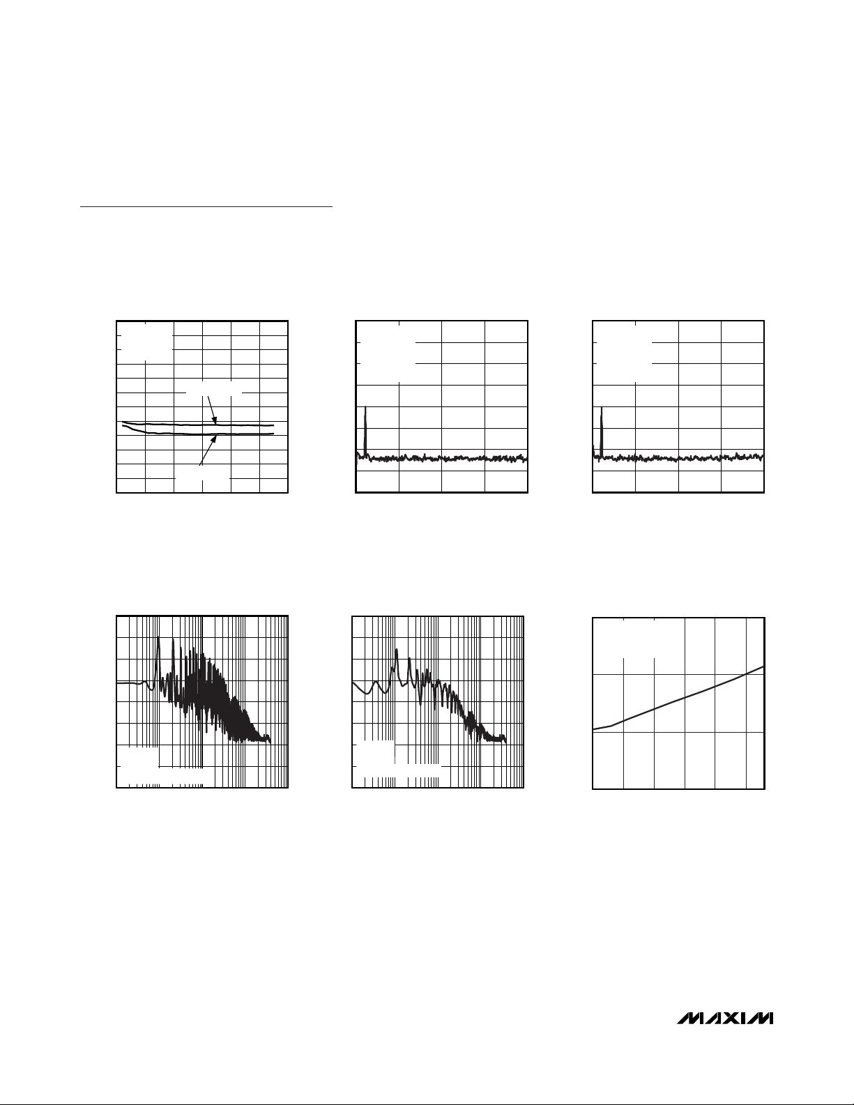
Typical Operating Characteristics (continued)
(VDD= PVDD= CPVDD= 3.3V, GND = PGND = CPGND = 0V, SHDN = VDD, I2C default gain settings (INA gain = +20dB, INB gain =
INC gain = 0dB, volume setting = 0dB, mono path gain = 0dB, SHDN = 1, SSM = 1). Speaker load resistors (R
LSP
) are terminated
between OUT_+ and OUT_-, headphone load resistors are terminated to GND, unless otherwise stated. C1 = C2 = C3 = 1µF. T
A
=
+25°C, unless otherwise noted.)
TOTAL HARMONIC DISTORTION PLUS NOISE
vs. OUTPUT POWER
MAX9775/76 toc07
OUTPUT POWER (W)
THD+N (%)
1.20.90.60.3
0.01
0.1
1
10
100
0.001
0 1.5
VDD = 5V
R
L
= 8Ω
f = 10kHz
f = 20Hz
f = 1kHz
TOTAL HARMONIC DISTORTION PLUS NOISE
vs. OUTPUT POWER
MAX9775/76 toc08
OUTPUT POWER (W)
THD+N (%)
0.60.40.2
0.01
0.1
1
10
100
0.001
0 0.8
VDD = 3.3V
R
L
= 4Ω
f = 10kHz
f = 20Hz
f = 1kHz
TOTAL HARMONIC DISTORTION PLUS NOISE
vs. OUTPUT POWER
MAX9775/76 toc09
OUTPUT POWER (W)
THD+N (%)
0.40.2
0.01
0.1
1
10
100
0.001
0 0.6
VDD = 3.3V
R
L
= 8Ω
f = 10kHz
f = 20Hz
f = 1kHz
TOTAL HARMONIC DISTORTION PLUS NOISE
vs. OUTPUT POWER
MAX9775/76 toc10
OUTPUT POWER (W)
THD+N (%)
1.20.90.60.3
0.01
0.1
1
10
100
0.001
0 1.5
VDD = 5V
R
L
= 8Ω
f = 1kHz
SSM
FFM
EFFICIENCY
vs. OUTPUT POWER
MAX9775/76 toc11
OUTPUT POWER (W)
EFFICIENCY (%)
3.22.41.60.8
10
20
30
40
50
60
70
80
90
100
0
0 4.0
VDD = 5V
f
IN
= 1kHz
P
OUT
= P
OUTL
+ P
OUTR
RL = 8Ω
RL = 4Ω
EFFICIENCY
vs. OUTPUT POWER
MAX9775/76 toc12
OUTPUT POWER (W)
EFFICIENCY (%)
1.61.20.80.4
10
20
30
40
50
60
70
80
90
100
0
0 2.0
VDD = 3.3V
f
IN
= 1kHz
P
OUT
= P
OUTL
+ P
OUTR
RL = 8Ω
RL = 4Ω
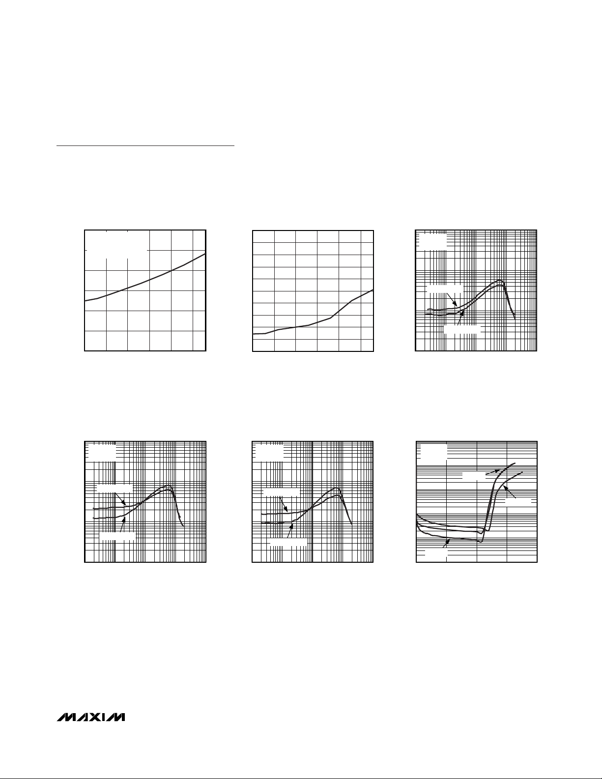
MAX9775/MAX9776
2 x 1.5W, Stereo Class D Audio Subsystem
with DirectDrive Headphone Amplifier
_______________________________________________________________________________________
9
Typical Operating Characteristics (continued)
(VDD= PVDD= CPVDD= 3.3V, GND = PGND = CPGND = 0V, SHDN = VDD, I2C default gain settings (INA gain = +20dB, INB gain =
INC gain = 0dB, volume setting = 0dB, mono path gain = 0dB, SHDN = 1, SSM = 1). Speaker load resistors (R
LSP
) are terminated
between OUT_+ and OUT_-, headphone load resistors are terminated to GND, unless otherwise stated. C1 = C2 = C3 = 1µF. T
A
=
+25°C, unless otherwise noted.)
OUTPUT POWER
vs. SUPPLY VOLTAGE
2200
RL = 4Ω
2000
f = 1kHz
1800
1600
1400
1200
1000
800
OUTPUT POWER (mW)
600
400
200
0
2.7
THD+N = 10%
THD+N = 1%
SUPPLY VOLTAGE (V)
OUTPUT POWER
vs. LOAD
1000
V
= 3.3V
DD
f = 1kHz
800
THD+N = 10%
600
400
OUTPUT POWER (W)
200
THD+N = 1%
0
1 100
10
LOAD (Ω)
1600
RL = 8Ω
f = 1kHz
1400
MAX9775/76 toc13
1200
1000
800
600
OUTPUT POWER (mW)
400
200
0
5.24.74.23.73.2
MAX9775/76 toc16
2.7
0
V
-10
V
RL = 8Ω
-20
-30
-40
-50
-60
-70
-80
POWER-SUPPLY REJECTION RATIO (dB)
-90
-100
10 100k
OUTPUT POWER
vs. SUPPLY VOLTAGE
THD+N = 10%
THD+N = 1%
5.24.73.2 3.7 4.2
SUPPLY VOLTAGE (V)
POWER-SUPPLY REJECTION RATIO
vs. FREQUENCY
= 3.3V
DD
= 100mV
IN
P-P
OUTR
OUTL
10k1k100
FREQUENCY (Hz)
MAX9775/76 toc14
OUTPUT POWER (W)
MAX9775/76 toc17
CROSSTALK (dB)
2.5
V
= 5V
DD
f = 1kHz
2.0
1.5
1.0
THD+N = 1%
0.5
0
1 100
CROSSTALK vs. FREQUENCY
0
OUT_ = 1V
-10
RL = 8Ω
-20
-30
-40
-50
-60
-70
-80
-90
-100
-110
-120
10 100 1k 10k 100k
LEFT TO RIGHT
OUTPUT POWER
vs. LOAD
THD+N = 10%
10
LOAD (Ω)
P-P
RIGHT TO LEFT
FREQUENCY (Hz)
MAX9775/76 toc15
MAX9775/6 toc18
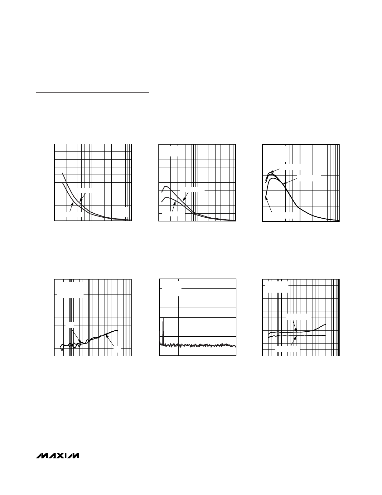
MAX9775/MAX9776
2 x 1.5W, Stereo Class D Audio Subsystem
with DirectDrive Headphone Amplifier
10 ______________________________________________________________________________________
Typical Operating Characteristics (continued)
(VDD= PVDD= CPVDD= 3.3V, GND = PGND = CPGND = 0V, SHDN = VDD, I2C default gain settings (INA gain = +20dB, INB gain =
INC gain = 0dB, volume setting = 0dB, mono path gain = 0dB, SHDN = 1, SSM = 1). Speaker load resistors (R
LSP
) are terminated
between OUT_+ and OUT_-, headphone load resistors are terminated to GND, unless otherwise stated. C1 = C2 = C3 = 1µF. T
A
=
+25°C, unless otherwise noted.)
CROSSTALK vs. INPUT AMPLITUDE
INPUT AMPLITUDE (V
RMS
)
CROSSTALK (dB)
MAX9775/6 toc19
0 0.1 0.2 0.3 0.4 0.5 0.6
-120
-110
-100
-90
-80
-70
-60
-50
-40
-30
-20
-10
0
fIN = 1kHz
R
L
= 8Ω
GAIN = +12dB
LEFT TO RIGHT
RIGHT TO LEFT
IN-BAND OUTPUT SPECTRUM
MAX9775/76 toc20
FREQUENCY (Hz)
OUTPUT MAGNITUDE (dBV)
15k10k5k
-120
-100
-80
-60
-40
-20
0
20
-140
0 20k
SSM MODE
R
L
= 8Ω
V
DD
= 3.3V
f
IN
= 1kHz
UNWEIGHTED
IN-BAND OUTPUT SPECTRUM
MAX9775/76 toc21
FREQUENCY (Hz)
OUTPUT MAGNITUDE (dBV)
15k10k5k
-120
-100
-80
-60
-40
-20
0
20
-140
0 20k
FFM MODE
R
L
= 8Ω
V
DD
= 3.3V
f
IN
= 1kHz
UNWEIGHTED
WIDEBAND OUTPUT SPECTRUM
FIXED-FREQUENCY MODE
FREQUENCY (MHz)
OUTPUT MAGNITUDE (dBV)
MAX9775/6 toc22
-140
-120
-100
-80
-60
-40
-20
0
20
0.1 1 10 100 1000
VDD = 5V
R
L
= 8Ω
INPUTS AC GROUNDED
WIDEBAND OUTPUT SPECTRUM
SPREAD-SPECTRUM MODE
FREQUENCY (MHz)
OUTPUT MAGNITUDE (dBV)
MAX9775 toc23
-140
-120
-100
-80
-60
-40
-20
0
20
0.1 1 10 100 1000
VDD = 5V
R
L
= 8Ω
INPUTS AC GROUNDED
MAX9775 SUPPLY CURRENT
vs. SUPPLY VOLTAGE
MAX9775/76 toc24
SUPPLY VOLTAGE (V)
SUPPLY CURRENT (mA)
5.24.74.23.73.2
15
20
25
10
2.7
SP MODE
INPUTS AC GROUNDED
OUTPUTS UNLOADED
MAX9775/MAX9776
2 x 1.5W, Stereo Class D Audio Subsystem
with DirectDrive Headphone Amplifier
______________________________________________________________________________________
11
Typical Operating Characteristics (continued)
(VDD= PVDD= CPVDD= 3.3V, GND = PGND = CPGND = 0V, SHDN = VDD, I2C default gain settings (INA gain = +20dB, INB gain =
INC gain = 0dB, volume setting = 0dB, mono path gain = 0dB, SHDN = 1, SSM = 1). Speaker load resistors (R
LSP
) are terminated
between OUT_+ and OUT_-, headphone load resistors are terminated to GND, unless otherwise stated. C1 = C2 = C3 = 1µF. T
A
=
+25°C, unless otherwise noted.)
MAX9776 SUPPLY CURRENT
vs. SUPPLY VOLTAGE
MAX9775/76 toc25
SUPPLY VOLTAGE (V)
SUPPLY CURRENT (mA)
5.24.74.23.73.2
6
8
10
12
14
16
4
2.7
SP MODE
INPUTS AC GROUNDED
OUTPUTS UNLOADED
SHUTDOWN SUPPLY CURRENT
vs. SUPPLY VOLTAGE
MAX9775/76 toc26
SUPPLY VOLTAGE (V)
SUPPLY CURRENT (nA)
5.24.74.23.73.2
10
20
30
40
50
60
70
80
90
100
0
2.7
TOTAL HARMONIC DISTORTION PLUS NOISE
vs. FREQUENCY
MAX9775/76 toc27
FREQUENCY (Hz)
THD+N (%)
10k1k100
0.01
0.1
1
0.001
10 100k
V
DD
= 5V
R
L
= 32Ω
P
OUT
= 20mW
P
OUT
= 40mW
TOTAL HARMONIC DISTORTION PLUS NOISE
vs. FREQUENCY
MAX9775/76 toc28
FREQUENCY (Hz)
THD+N (%)
10k1k100
0.01
0.1
1
0.001
10 100k
V
DD
= 3.3V
R
L
= 16Ω
P
OUT
= 20mW
P
OUT
= 40mW
TOTAL HARMONIC DISTORTION PLUS NOISE
vs. FREQUENCY
MAX9775/76 toc29
FREQUENCY (Hz)
THD+N (%)
10k1k100
0.01
0.1
1
0.001
10 100k
V
DD
= 3.3V
R
L
= 32Ω
P
OUT
= 10mW
P
OUT
= 40mW
TOTAL HARMONIC DISTORTION PLUS NOISE
vs. OUTPUT POWER
MAX9775/76 toc30
OUTPUT POWER (mW)
THD+N (%)
604020
0.01
0.1
1
10
100
0.001
080
VDD = 5V
R
L
= 32Ω
f = 10kHz
f = 20Hz
f = 1kHz

MAX9775/MAX9776
2 x 1.5W, Stereo Class D Audio Subsystem
with DirectDrive Headphone Amplifier
12 ______________________________________________________________________________________
Typical Operating Characteristics (continued)
(VDD= PVDD= CPVDD= 3.3V, GND = PGND = CPGND = 0V, SHDN = VDD, I2C default gain settings (INA gain = +20dB, INB gain =
INC gain = 0dB, volume setting = 0dB, mono path gain = 0dB, SHDN = 1, SSM = 1). Speaker load resistors (R
LSP
) are terminated
between OUT_+ and OUT_-, headphone load resistors are terminated to GND, unless otherwise stated. C1 = C2 = C3 = 1µF. T
A
=
+25°C, unless otherwise noted.)
TOTAL HARMONIC DISTORTION PLUS NOISE
vs. OUTPUT POWER
OUTPUT POWER (mW)
THD+N (%)
MAX9775 toc31
0 30 60 90 120
0.001
0.01
0.1
1
10
100
f = 20Hz
f = 1kHz
f = 10kHz
VDD = 3.3V
R
L
= 16Ω
TOTAL HARMONIC DISTORTION PLUS NOISE
vs. OUTPUT POWER
MAX9775/76 toc32
OUTPUT POWER (mW)
THD+N (%)
604020
0.01
0.1
1
10
100
0.001
080
VDD = 3.3V
R
L
= 32Ω
f = 10kHz
f = 20Hz
f = 1kHz
TOTAL HARMONIC DISTORTION PLUS NOISE
vs. COMMON-MODE VOLTAGE
COMMON-MODE VOLTAGE (V)
THD+N (%)
MAX9775/6 toc33
0 0.5 1.0 1.5 2.0 2.5
0.001
0.01
0.1
1
10
100
VDD = 3.3V
f
IN
= 1kHz
P
OUT
= 30mW
GAIN = +3dB
R
L
= 32Ω
POWER DISSIPATION
vs. OUTPUT POWER
MAX9775/76 toc34
TOTAL OUTPUT POWER (mW)
POWER DISSIPATION (mW)
8040
50
100
150
200
250
300
350
400
450
500
0
0 120
V
DD
= 5V
f = 1kHz
R
L
= 32Ω
P
OUT
= P
OUTR
+ P
OUTL
POWER DISSIPATION
vs. OUTPUT POWER
MAX9775/76 toc35
TOTAL OUTPUT POWER (mW)
POWER DISSIPATION (mW)
1208040
50
100
150
200
250
300
350
400
450
500
0
0 160
V
DD
= 3.3V
f = 1kHz
P
OUT
= P
OUTR
+ P
OUTL
RL = 16Ω
RL = 32Ω
OUTPUT POWER
vs. SUPPLY VOLTAGE
MAX9775/76 toc36
SUPPLY VOLTAGE (V)
OUTPUT POWER (mW)
5.24.74.23.73.2
35
40
45
50
55
60
65
30
2.7
THD+N = 10%
THD+N = 1%
RL = 32Ω
f = 1kHz
MAX9775/MAX9776
2 x 1.5W, Stereo Class D Audio Subsystem
with DirectDrive Headphone Amplifier
______________________________________________________________________________________
13
Typical Operating Characteristics (continued)
(VDD= PVDD= CPVDD= 3.3V, GND = PGND = CPGND = 0V, SHDN = VDD, I2C default gain settings (INA gain = +20dB, INB gain =
INC gain = 0dB, volume setting = 0dB, mono path gain = 0dB, SHDN = 1, SSM = 1). Speaker load resistors (R
LSP
) are terminated
between OUT_+ and OUT_-, headphone load resistors are terminated to GND, unless otherwise stated. C1 = C2 = C3 = 1µF. T
A
=
+25°C, unless otherwise noted.)
OUTPUT POWER
vs. LOAD
MAX9775/76 toc37
LOAD (Ω)
OUTPUT POWER (mW)
100
20
40
60
80
100
120
140
160
180
200
0
10 1000
THD+N = 10%
THD+N = 1%
V
DD
= 5V
f = 1kHz
OUTPUT POWER
vs. LOAD
MAX9775/76 toc38
LOAD (Ω)
OUTPUT POWER (mW)
100
20
40
60
80
100
120
140
160
180
200
0
10 1000
THD+N = 10%
THD+N = 1%
V
DD
= 3.3V
f = 1kHz
OUTPUT POWER vs. LOAD RESISTANCE
AND CHARGE-PUMP CAPACITOR SIZE
LOAD (Ω)
OUTPUT POWER (mW)
MAX9775/6 toc39
0
20
40
60
80
100
10 100 1000
C1 = C2 = 2.2μF
VDD = 3.3V
f
= 1kHz
THD+N = 1%
C1 = C2 = 1μF
C1 = C2 = 0.68μF
POWER-SUPPLY REJECTION RATIO
vs. FREQUENCY
FREQUENCY (Hz)
POWER-SUPPLY REJECTION RATIO (dB)
MAX9775/6 toc40
-100
-90
-80
-70
-60
-50
-40
-30
-20
-10
0
10 100 1k 10k 100k
HPL
HPR
VDD = 3.3V
V
IN
= 100mV
P-P
RL = 32Ω
OUTPUT FREQUENCY SPECTRUM
MAX9775/76 toc41
FREQUENCY (Hz)
OUTPUT MAGNITUDE (dBV)
15k10k5k
-120
-100
-80
-60
-40
-20
0
20
-140
0 20k
V
DD
= 3.3V
f
= 1kHz
R
L
= 32Ω
CROSSTALK vs. FREQUENCY
FREQUENCY (Hz)
CROSSTALK (dB)
MAX9775/6 toc42
-120
-110
-100
-90
-80
-70
-60
-50
-40
-30
-20
-10
0
10 100 1k 10k 100k
OUT_ = 1V
P-P
RL = 32Ω
LEFT TO RIGHT
RIGHT TO LEFT
MAX9775/MAX9776
2 x 1.5W, Stereo Class D Audio Subsystem
with DirectDrive Headphone Amplifier
14 ______________________________________________________________________________________
Typical Operating Characteristics (continued)
(VDD= PVDD= CPVDD= 3.3V, GND = PGND = CPGND = 0V, SHDN = VDD, I2C default gain settings (INA gain = +20dB, INB gain =
INC gain = 0dB, volume setting = 0dB, mono path gain = 0dB, SHDN = 1, SSM = 1). Speaker load resistors (R
LSP
) are terminated
between OUT_+ and OUT_-, headphone load resistors are terminated to GND, unless otherwise stated. C1 = C2 = C3 = 1µF. T
A
=
+25°C, unless otherwise noted.)
CROSSTALK vs. INPUT AMPLITUDE
INPUT AMPLITUDE (V
RMS
)
CROSSTALK (dB)
MAX9775 toc43
0 0.4 0.8 1.2
-120
-110
-100
-90
-80
-70
-60
-50
-40
-30
-20
-10
0
fIN = 1kHz
R
L
= 32Ω
GAIN = +3dB
LEFT TO RIGHT
RIGHT TO LEFT
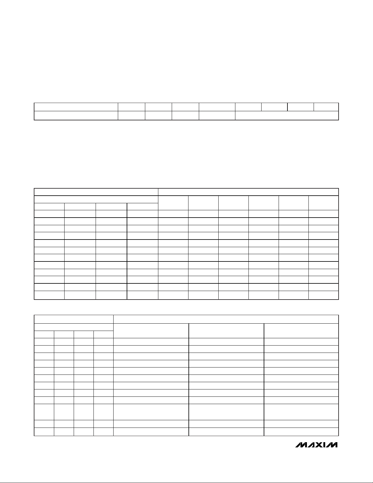
TURN-ON RESPONSE
MAX9775/76 toc44
10ms/div
SCL
2V/div
SPEAKER
OUTPUT
50mA/div
HEADPHONE
OUTPUT
2V/div
TURN-OFF RESPONSE
MAX9775/76 toc45
10ms/div
SCL
2V/div
SPEAKER
OUTPUT
50mA/div
HEADPHONE
OUTPUT
2V/div
MUTE-ON RESPONSE
MAX9775/76 toc46
10ms/div
SCL
2V/div
SPEAKER
OUTPUT
50mA/div
HEADPHONE
OUTPUT
2V/div
MUTE-OFF RESPONSE
MAX9775/76 toc47
10ms/div
SCL
2V/div
SPEAKER
OUTPUT
50mA/div
HEADPHONE
OUTPUT
2V/div

MAX9775/MAX9776
2 x 1.5W, Stereo Class D Audio Subsystem
with DirectDrive Headphone Amplifier
______________________________________________________________________________________ 15
Pin Description—MAX9775
PIN NAME FUNCTION
F1 PV
E1 OUTL- Negative Left-Speaker Output
D2 SCL Serial Clock Input. Connect a 1kΩ pullup resistor from SCL to VDD.
D1, F3 PGND Power Ground
C1 OUTL+ Positive Left-Speaker Output
C2 SDA Serial Data Input. Connect a 1kΩ pullup resistor from SDA to VDD.
B1 CL_L 3D External Capacitor 3. Connect a 2.2nF capacitor to GND.
B2 CL_H 3D External Capacitor 4. Connect a 22nF capacitor to GND.
A1 CPV
A2 C1P Charge-Pump Flying Capacitor Positive Terminal
B3 VBIAS Common-Mode Bias
A3 CPGND Charge-Pump GND
A4 C1N Charge-Pump Flying Capacitor Negative Terminal
B4 INC1 Input C1. Left input or positive input (see Table 5a).
A5 CPV
A6 HPL Left Headphone Output
B5 V
B6 HPR Right Headphone Output
C5 INC2 Input C2. Right input or negative input (see Table 5a).
C6 OUTRx Mono Receiver Output
D6 V
D5 INB2 Input B2. Right input or negative input (see Table 5a).
E6 CR_L 3D External Capacitor 1. Connect a 2.2nF capacitor to GND.
E5 INB1 Input B1. Left input or positive input (see Table 5a).
F6 GND Analog Ground
F5 CR_H 3D External Capacitor 2. Connect a 22nF capacitor to GND.
E4 INA2 Input A2. Right input or negative input (see Table 5a).
F4 OUTR+ Positive Right Speaker Output
E3 INA1 Input A1. Left input or positive input (see Table 5a).
F2 OUTR- Negative Right Speaker Output
E2 SHDN Active-Low Hardware Shutdown
—EP
DD
DD
SS
SS
DD
Class D Power Supply
Charge-Pump Power Supply
Charge-Pump Output. Connect to VSS.
Headphone Amplifier Negative Power Supply. Connect to CPVSS.
Analog Power Supply
Exposed Pad. The external pad lowers the package’s thermal impedance by providing a
direct heat conduction path from the die to the PCB. The exposed pad is internally
connected to GND. Connect the exposed thermal pad to the GND plane.

MAX9775/MAX9776
2 x 1.5W, Stereo Class D Audio Subsystem
with DirectDrive Headphone Amplifier
16 ______________________________________________________________________________________
Pin Description—MAX9776
PIN
TQFN UCSP
1F1PVDDClass D Power Supply
2 E1 OUT- Negative Left-Speaker Output
3 D2 SCL Serial Clock Input. Connect a 1kΩ pullup resistor from SCL to VDD.
4, 29 D1, F3 PGND Power Ground
5 C1 OUT+ Positive Left-Speaker Output
6 C2 SDA Serial Data Input. Connect a 1kΩ pullup resistor from SDA to VDD.
7, 8, 23,
26, 28, 31
9 A1 CPV
10 A2 C1P Charge-Pump Flying Capacitor Positive Terminal
11 B3 VBIAS Common-Mode Bias
12 A3 CPGND Charge-Pump GND
13 A4 C1N Charge-Pump Flying Capacitor Negative Terminal
14 B4 INC1 Input C1. Left input or positive input (see Table 5a).
15 A5 CPV
16 A6 HPL Left Headphone Output
17 B5 V
18 B6 HPR Right Headphone Output
19 C5 INC2 Input C2. Right input or negative input (see Table 5a).
20 C6 OUTRx Mono Receiver Output
21 D6 V
22 D5 INB2 Input B2. Right input or negative input (see Table 5a).
24 E5 INB1 Input B1. Left input or positive input (see Table 5a).
25 F6 GND Analog Ground
27 E4 INA2 Input A2. Right input or negative input (see Table 5a).
30 E3 INA1 Input A1. Left input or positive input (see Table 5a).
32 E2 SHDN Active-Low Hardware Shutdown
EP — EP
B1, B2,
E6, F2,
F4, F5
NAME FUNCTION
I.C.
Internal Connection. Leave unconnected. This pin is internally connected to the signal path.
Do not connect together or to any other pin.
Charge-Pump Power Supply
DD
Charge-Pump Output. Connect to VSS.
SS
Headphone Amplifier Negative Power Supply. Connect to CPVSS.
SS
Analog Power Supply
DD
Exposed Pad. The external pad lowers the package’s thermal impedance by providing a
direct heat conduction path from the die to the PCB. The exposed pad is internally connected
to GND. Connect the exposed thermal pad to the GND plane.

MAX9775/MAX9776
2 x 1.5W, Stereo Class D Audio Subsystem
with DirectDrive Headphone Amplifier
______________________________________________________________________________________ 17
Typical Application Circuits
10kΩ
V
DD
C2
1μF
CPVSSV
SS
15 (A5) 17 (B5)
13 (A4)
C1N
12 (A3)
1μF
1μF
1μF
1μF
1μF
1μF
1μF
CPGND
C1P
CPV
INA1
INA2
INB1
INB2
INC1
INC2
VBIAS
CHARGE
10 (A2)
9 (A1)
DD
30 (E3)
27 (E4)
24 (E5)
22 (D5)
14 (B4)
19 (C5)
11 (B3)
PUMP
INPUT A: 0dB,
6dB, OR 20dB
INPUT B: 0dB
OR 6dB
INPUT C: 0dB
OR 6dB
INPUT
MIXER
C1
1μF
V
DD
C3
1μF
21 (D6)
RIGHT
VOLUME
LEFT
VOLUME
MONO
VOLUME
1μF
V
DD
OUTPUT
MIXER
V
DD
PV
1 (F1)
MAXIM 3D
SOUND
DD
DirectDrive
3dB
3dB
3dB
12dB
CLASS D
AMPLIFIER
12dB
CLASS D
AMPLIFIER
1μF0.1μF
HPL
16 (A6)
HPR
18 (B6)
OUTRx
20 (C6)
OUTL+
5 (C1)
2 (E1)
OUTL-
28 (F4)
OUTR+
31 (F2)
OUTR-
6 (C2)
SDA
SCL
SHDN
3 (D2)
32 (E2)
GND
I2C CONTROL
4 (D1) 29 (F3)
PGND
PGND
23 (E6)25 (F6)
CR_L
2.2nF
MAX9775
3D CIRCUIT
26 (F5)
CR_H
22nF
7 (B1)
CL_L
2.2nF
8 (B2)
CL_H
22nF

MAX9775/MAX9776
2 x 1.5W, Stereo Class D Audio Subsystem
with DirectDrive Headphone Amplifier
18 ______________________________________________________________________________________
Typical Application Circuits (continued)
CPVSSV
SS
15 (A5) 17 (B5)
13 (A4)
C1N
12 (A3)
1μF
1μF
1μF
1μF
1μF
1μF
1μF
CPGND
C1P
CPV
INA1
INA2
INB1
INB2
INC1
INC2
VBIAS
CHARGE
10 (A2)
9 (A1)
DD
30 (E3)
27 (E4)
24 (E5)
22 (D5)
14 (B4)
19 (C5)
11 (B3)
PUMP
INPUT A: 0dB,
6dB, OR 20dB
INPUT B: 0dB
OR 6dB
INPUT C: 0dB
OR 6dB
10kΩ
C1
1μF
V
DD
C3
1μF
C2
1μF
INPUT
MIXER
RIGHT
VOLUME
LEFT
VOLUME
MONO
VOLUME
V
DD
21 (D6)
V
DD
OUTPUT
MIXER
1μF
V
DD
1 (F1)
1μF0.1μF
PV
DD
DirectDrive
16 (A6)
18 (B6)
20 (C6)
5 (C1)
2 (E1)
HPL
HPR
OUTRx
OUT+
OUT-
3dB
3dB
3dB
12dB
CLASS D
AMPLIFIER
6 (C2)
SDA
SCL
SHDN
3 (D2)
32 (E2)
I2C CONTROL
25 (F6)
GND
4 (D1) 29 (F3)
PGNDPGND
MAX9776

MAX9775/MAX9776
2 x 1.5W, Stereo Class D Audio Subsystem
with DirectDrive Headphone Amplifier
______________________________________________________________________________________ 19
Detailed Description
The MAX9775/MAX9776 ultra-low-EMI, filterless, Class D
audio power amplifiers feature several improvements to
switch-mode amplifier technology. The MAX9775/
MAX9776 feature active emissions limiting circuitry to
reduce EMI. Zero dead-time technology maintains stateof-the-art efficiency and THD+N performance by allowing
the output FETs to switch simultaneously without crossconduction. A unique filterless modulation scheme and
spread-spectrum modulation create compact, flexible,
low-noise, efficient audio power amplifiers while
occupying minimal board space. The differential input
architecture reduces common-mode noise pickup with or
without the use of input-coupling capacitors. The
MAX9775/MAX9776 can also be configured as singleended input amplifiers without performance degradation.
The MAX9775/MAX9776 feature three fully differential
input pairs (INA_, INB_, INC_) that can be configured
as stereo single-ended or mono differential inputs. I2C
provides control for input configuration, volume level,
and mixer configuration. The MAX9775’s 3D enhancement feature widens the stereo sound field to improve
stereo imaging when stereo speakers are placed in
close proximity.
DirectDrive allows the headphone and mono receiver
amplifiers to output ground-referenced signals from a
single supply, eliminating the need for large DC-blocking capacitors. Comprehensive click-and-pop suppression minimizes audible transients during the turn-on
and turn-off of amplifiers.
Class D Speaker Amplifier
Comparators monitor the audio inputs and compare the
complementary input voltages to a sawtooth waveform.
The comparators trip when the input magnitude of the
sawtooth exceeds their corresponding input voltage. The
active emissions limiting circuitry slightly reduces the
turn-on rate of the output H-bridge by slew-rate limiting
the comparator output pulse. Both comparators reset at
a fixed time after the rising edge of the second comparator trip point, generating a minimum-width pulse
(t
ON(MIN)
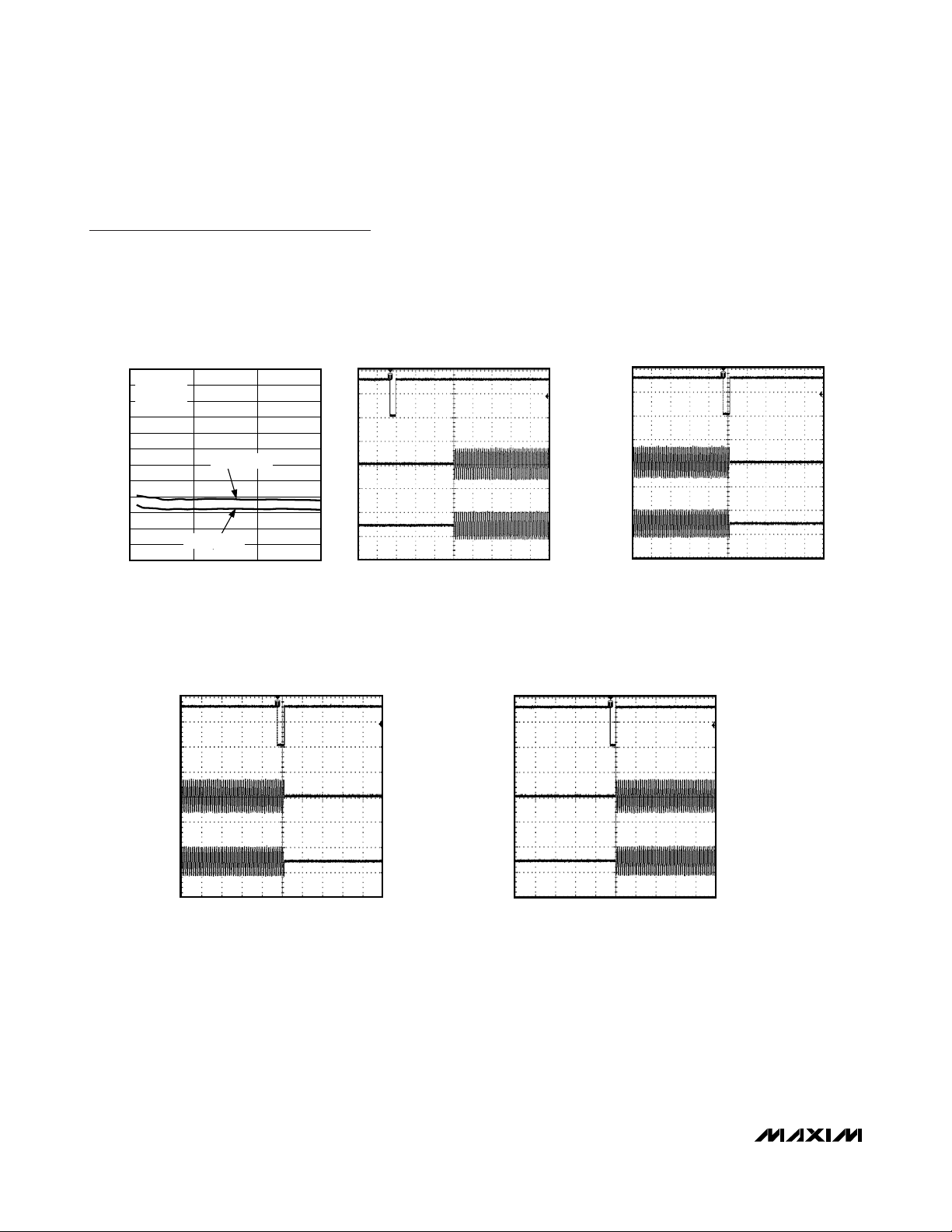
,100ns typ) at the output of the second comparator (Figure 1). As the input voltage increases or
decreases, the duration of the pulse at one output
increases while the other output pulse duration remains
the same. This causes the net voltage across the speaker (V
OUT+
- V
OUT-
) to change. The minimum-width pulse
helps the devices to achieve high levels of linearity.
Figure 1. Outputs with an Input Signal Applied
t
SW
V
IN-
V
IN+
OUT-
OUT+
V
- V
OUT+
OUT-
t
ON(MIN)

MAX9775/MAX9776
Operating Modes
Fixed-Frequency Modulation
The MAX9775/MAX9776 feature a fixed-frequency
modulation mode with a 1.1MHz switching frequency,
set through the I2C interface (Table 2). In fixed-frequency modulation mode, the frequency spectrum of the
Class D output consists of the fundamental switching
frequency and its associated harmonics (see the
Wideband Output Spectrum Fixed-Frequency Mode
graph in the
Typical Operating Characteristics
).
Spread-Spectrum Modulation
The MAX9775/MAX9776 feature a unique spread-spectrum modulation that flattens the wideband spectral components. Proprietary techniques ensure that the
cycle-to-cycle variation of the switching period does not
degrade audio reproduction or efficiency (see the
Typical Operating Characteristics
). Select spread-spec-
trum modulation mode through the I2C interface (Table
2). In spread-spectrum modulation mode, the switching
frequency varies randomly by ±30kHz around the center
frequency (1.16MHz). The modulation scheme remains
the same, but the period of the sawtooth waveform
changes from cycle to cycle (Figure 2). Instead of a
large amount of spectral energy present at multiples of
the switching frequency, the energy is now spread over
a bandwidth that increases with frequency. Above a few
megahertz, the wideband spectrum looks like white
noise for EMI purposes (see Figure 3).
2 x 1.5W, Stereo Class D Audio Subsystem
with DirectDrive Headphone Amplifier
20 ______________________________________________________________________________________
V
OUT+
- V
OUT-
t
SW
t
SW
t
SW
t
SW
V
IN-
V
IN+
OUT+
OUT-
t
ON(MIN)
Figure 2. Output with an Input Signal Applied (Spread-Spectrum Modulation Mode)

MAX9775/MAX9776
2 x 1.5W, Stereo Class D Audio Subsystem
with DirectDrive Headphone Amplifier
______________________________________________________________________________________ 21
Figure 3. EMI with 76mm of Speaker Cable
40.0
35.0
EN55022B LIMIT
30.0 60.0 80.0 100.0 120.0 140.0 160.0 180.0 200.0 220.0 240.0 260.0 280.0 300.0
FREQUENCY (MHz)
AMPLITUDE (dBμV/m)
30.0
25.0
20.0
15.0
10.0
5.0

MAX9775/MAX9776
2 x 1.5W, Stereo Class D Audio Subsystem
with DirectDrive Headphone Amplifier
22 ______________________________________________________________________________________
Filterless Modulation/Common-Mode Idle
The MAX9775/MAX9776 use Maxim’s unique modulation scheme that eliminates the LC filter required by traditional Class D amplifiers, improving efficiency,
reducing component count, conserving board space
and system cost. Conventional Class D amplifiers output a 50% duty-cycle square wave when no signal is
present. With no filter, the square wave appears across
the load as a DC voltage, resulting in finite load current,
increasing power consumption, especially when idling.
When no signal is present at the input of the
MAX9775/MAX9776, the outputs switch as shown in
Figure 4. Because the MAX9775/MAX9776 drive the
speaker differentially, the two outputs cancel each
other, resulting in no net idle mode voltage across the
speaker, minimizing power consumption.
DirectDrive
Traditional single-supply headphone amplifiers have
outputs biased at a nominal DC voltage (typically half
the supply) for maximum dynamic range. Large coupling capacitors are needed to block this DC bias from
the headphone. Without these capacitors, a significant
amount of DC current flows to the headphone, resulting
in unnecessary power dissipation and possible damage to both headphone and headphone amplifier.
Maxim’s DirectDrive architecture uses a charge pump to
create an internal negative supply voltage. This allows the
headphone outputs of the MAX9775/MAX9776 to be
biased at GND, almost doubling dynamic range while
operating from a single supply. With no DC component,
there is no need for the large DC-blocking capacitors.
Instead of two large (220µF, typ) tantalum capacitors, the
MAX9775/MAX9776 charge pump requires two small
ceramic capacitors, conserving board space, reducing
cost, and improving the frequency response of the headphone amplifier. See the Output Power vs. Load
Resistance and Charge-Pump Capacitor Size graph in
the
Typical Operating Characteristics
for details of the
possible capacitor sizes. There is a low DC voltage on
the amplifier outputs due to amplifier offset. However, the
offset of the MAX9775/MAX9776 is typically 1.4mV,
which, when combined with a 32Ω load, results in less
than 44nA of DC current flow to the headphones.
In addition to the cost and size disadvantages of the
DC-blocking capacitors required by conventional headphone amplifiers, these capacitors limit the amplifier’s
low-frequency response and can distort the audio signal. Previous attempts at eliminating the output-coupling capacitors involved biasing the headphone return
(sleeve) to the DC bias voltage of the headphone
amplifiers. This method raises some issues:
1) The sleeve is typically grounded to the chassis.
Using the midrail biasing approach, the sleeve must
be isolated from system ground, complicating product design.
2) During an ESD strike, the driver’s ESD structures are
the only path to system ground. Thus, the amplifier
must be able to withstand the full ESD strike.
3) When using the headphone jack as a lineout to
other equipment, the bias voltage on the sleeve may
conflict with the ground potential from other equipment, resulting in possible damage to the amplifiers.
VIN = 0V
OUT-
OUT+
V
OUT+
- V
OUT-
= 0V
Figure 4. Outputs with No Input Signal

Charge Pump
The MAX9775/MAX9776 feature a low-noise charge
pump. The switching frequency of the charge pump is
half the switching frequency of the Class D amplifier,
regardless of the operating mode. The nominal switching frequency is well beyond the audio range, and thus
does not interfere with the audio signals, resulting in an
SNR of 93dB. Although not typically required, additional high-frequency noise attenuation can be achieved by
increasing the size of C2 (see the
Typical Application
Circuits
). The charge pump is active in both speaker
and headphone modes.
3D Enhancement
The MAX9775 features a 3D stereo enhancement function, allowing the MAX9775 to widen the stereo sound field
and immerse the listener in a cleaner, richer sound experience. Note the MAX9776, mono Class D speaker amplifier
does not feature 3D stereo enhancement.
As stereo speaker applications become more compact,
the quality of stereophonic sound is jeopardized.
With Maxim’s 3D stereo enhancement, it is possible to
emulate stereo sound in situations where the speakers
must be positioned close together. As shown in Figure
6, wave interference can be used to cancel the left
channel in the vicinity of the listener’s right ear and vice
versa. This technique can yield an apparent separation
between the speakers that is a factor of four or greater
than the actual physical separation.
The external capacitors CL_L, CL_H, CR_L, and CR_H
set the starting and stopping range of the 3D effect.
CL_H and CR_H are for the lower limit (in the MAX9775
Typical Application Circuit
, it is 1kHz), CR_L and CL_L
are for the higher limit (10kHz). The internal resistor is
typically 7kΩ and the frequencies are calculated as:
where R = 7kΩ and C = CR_H and CL_H.
where R = 7kΩ and C = CR_L and CL_L.
For example, with CR_L = CL_L = 2.2nF and CR_H =
CL_H = 22nF, the 3D start frequency is 1kHz and the
3D stop frequency is 10kHz.
Enabling the 3D sound effect results in an apparent 6dB
gain because the internal left and right signals are mixed
together. This gain can be nulled by volume adjusting
the left and right signals. The volume control can be programmed through the I2C-compatible interface to compensate for the extra 6dB increase in gain. For example,
MAX9775/MAX9776
2 x 1.5W, Stereo Class D Audio Subsystem
with DirectDrive Headphone Amplifier
______________________________________________________________________________________ 23
Figure 5. Traditional Amplifier Output vs. MAX9775/MAX9776
DirectDrive Output
Figure 6. MAX9775 3D Stereo Enhancement
Q
V
DD
RIGHT
R
V
OUT
CONVENTIONAL DRIVER-BIASING SCHEME
V
OUT
DirectDrive BIASING SCHEME
VDD / 2
GND
+V
DD
GND
-V
DD
+
I
L
d
I
R
+
LEFT
Q
L
RIGHT
LISTENER
LEFT
3
D START
_ =
1
2
RC
π
3
D STOP
_ =
1
2
RC
π

MAX9775/MAX9776
if the right and left volume controls are set for a maximum gain 0dB (11111 in Table 7, IN+6dB = 0 from Table
10) before the 3D effect is activated, the volume control
should be programmed to -6dB (11001 in Table 7)
immediately after the 3D effect has been activated.
Signal Path
The audio inputs of the MAX9775/MAX9776—INA, INB,
and INC—are preamplified and then mixed by the input
mixer to create three internal signals: Left (L), Right (R),
and Mono (M). Tables 5a and 5b show how the inputs
are mixed to create L, R, and M. These signals are then
independently volume adjusted by the L, R, and M volume control and routed to the output mixer. The output
mixer mixes the internal L, R, and M signals to create a
variety of audio mixes that are output to the headphone
speaker and mono receiver amplifiers. Figure 6 shows
the signal path that the audio signals take.
Signal amplification takes place in three stages. In the
first stage, the inputs (INA, INB, and INC) are preamplified. The amount by which each input is amplified
is determined by the bits INA+20dB (B4 in the Input
Mode Control Register) and IN+6dB (B3 in the Global
Control Register). After preamplification, they are mixed
in the Input Mixer to create the internal signals L, R,
and M.
In the second stage of amplification, the internal L, R,
and M signals are independently volume adjusted.
Finally, each output amplifier has its own internal gain.
The speaker, headphone, and mono receiver amplifiers
have fixed gains of 12dB, 3dB, and 3dB, respectively.
Current-Limit and Thermal Protection
The MAX9775/MAX9776 feature current limiting and
thermal protection to protect the device from short circuits and overcurrent conditions. The headphone
amplifier pulses in the event of an overcurrent condition
with a pulse every 100µs as long as the condition is
present. Should the current still be high, the above
cycle is repeated. The speaker amplifier current-limit
protection clamps the output current without shutting
down the output. This can result in a distorted output.
Current is limited to 1.6A in the speaker amplifiers and
170mA in the headphone and mono receiver amplifiers.
The MAX9775/MAX9776 have thermal protection that
disables the device at +150°C until the temperature
decreases to +120°C.
2 x 1.5W, Stereo Class D Audio Subsystem
with DirectDrive Headphone Amplifier
24 ______________________________________________________________________________________
Figure 7. Signal Path
-75dB TO 0dB
RVOL
PREAMPLIFIER
INPUT
INPUT A:
0dB, 6dB, 20dB
INPUT B AND C:
0dB, 6dB
INPUT
MIXER
MONO
-75dB TO 0dB
LVOL
OUTPUT
MIXER
-75dB TO 0dB0dB TO 6dB
MVOLMONO+6dB
12dB
SPEAKER
3dB
HEADPHONE
3dB
RECEIVER

Click-and-Pop Suppression
In conventional single-supply headphone amplifiers, the
output-coupling capacitor is a major contributor of audible clicks and pops. Upon startup, the amplifier charges
the coupling capacitor to its bias voltage, typically half the
supply. Likewise, during shutdown, the capacitor is discharged to GND. This results in a DC shift across the
capacitor, which, in turn, appears as an audible transient
at the speaker. Since the MAX9775/MAX9776 headphone
amplifier does not require output-coupling capacitors, this
problem does not arise.
In most applications, the output of the preamplifier driving the MAX9775/MAX9776 has a DC bias of typically
half the supply. During startup, the input-coupling
capacitor is charged to the preamplifier’s DC bias voltage, resulting in a DC shift across the capacitor and an
audible click/pop. An internal delay of 30ms eliminates
the click/pop caused by the input filter.
Shutdown
The MAX9775/MAX9776 feature a 0.1µA hard shutdown
mode that reduces power consumption to extend battery
life and a soft shutdown where current consumption is
typically 8.5µA. Hard shutdown is controlled by connecting the SHDN pin to GND, disabling the amplifiers, bias
circuitry, charge pump, and I2C. In shutdown, the headphone amplifier output impedance is 1.4kΩ and the
speaker output impedance is 300kΩ. Similarly, the
MAX9775/MAX9776 enter soft-shutdown when the SHDN
bit = 0 (see Table 2). The I
2
C interface is active and the
contents of the command register are not affected when
in soft-shutdown. This allows the master to write to the
MAX9775/MAX9776 while in shutdown. The I2C interface
is completely disabled in hardware shutdown. When the
MAX9775/MAX9776 are re-enabled the default settings
are applied (see Table 3).
I2C Interface
The MAX9775/MAX9776 feature an I2C 2-wire serial
interface consisting of a serial data line (SDA) and a
serial clock line (SCL). SDA and SCL facilitate communication between the MAX9775/MAX9776 and the master at clock rates up to 400kHz. Figure 8 shows the
2-wire interface timing diagram. The MAX9775/
MAX9776 are receive-only slave devices relying on the
master to generate the SCL signal. The master, typically a microcontroller, generates SCL and initiates data
transfer on the bus. The MAX9775/MAX9776 cannot
write to the SDA bus except to acknowledge the receipt
of data from the master. The MAX9775/MAX9776 will
not acknowledge a read command from the master.
A master device communicates to the MAX9775/
MAX9776 by transmitting the proper address followed
by the data word. Each transmit sequence is framed by
a START (S) or REPEATED START (Sr) condition and a
STOP (P) condition. Each word transmitted over the
bus is 8 bits long and is always followed by an
acknowledge clock pulse.
The MAX9775/MAX9776 SDA line operates as both an
input and an open-drain output. A pullup resistor,
greater than 500Ω, is required on the SDA bus. The
MAX9775/MAX9776 SCL line operates as an input only.
A pullup resistor (greater than 500Ω) is required on
SCL if there are multiple masters on the bus or if the
master in a single-master system has an open-drain
SCL output. Series resistors in line with SDA and SCL
are optional. Series resistors protect the digital inputs of
the MAX9775/MAX9776 from high-voltage spikes on
the bus lines, and minimize crosstalk and undershoot of
the bus signals.
MAX9775/MAX9776
2 x 1.5W, Stereo Class D Audio Subsystem
with DirectDrive Headphone Amplifier
______________________________________________________________________________________ 25
Figure 8. 2-Wire Serial-Interface Timing Diagram
SDA
t
SU, DAT
t
LOW
SCL
t
t
HD, STA
START
CONDITION
HIGH
t
R
t
F
t
HD, DAT
t
SU, STA
REPEATED
START
CONDITION
t
HD, STA
t
BUF
t
SP
t
SU, STO
STOP
CONDITION
START
CONDITION

MAX9775/MAX9776
Bit Transfer
One data bit is transferred during each SCL cycle. The
data on SDA must remain stable during the high period
of the SCL pulse. Changes in SDA while SCL is high
are control signals (see the
START and STOP
Conditions
section). SDA and SCL idle high when the
I
2
C bus is not busy.
START and STOP Conditions
A master device initiates communication by issuing a
START condition. A START condition is a high-to-low
transition on SDA with SCL high. A STOP condition is a
low-to-high transition on SDA while SCL is high (Figure
9). A START (S) condition from the master signals the
beginning of a transmission to the MAX9775/MAX9776.
The master terminates transmission, and frees the bus,
by issuing a STOP (P) condition. The bus remains active
if a REPEATED START (Sr) condition is generated
instead of a STOP condition.
Early STOP Conditions
The MAX9775/MAX9776 recognize a STOP condition at
any point during data transmission except if the STOP
condition occurs in the same high pulse as a START
condition.
Slave Address
The MAX9775/MAX9776 are available with one preset
slave address (see Table 1). The address is defined as
the seven most significant bits (MSBs) followed by the
Read/Write bit. The address is the first byte of information sent to the MAX9775/MAX9776 after the START
condition. The MAX9775/MAX9776 are slave devices
only capable of being written to. The Read/Write bit
should be a zero when configuring the MAX9775/
MAX9776.
Acknowledge
The acknowledge bit (ACK) is a clocked 9th bit that the
MAX9775/MAX9776 use to handshake receipt of each
byte of data (see Figure 10). The MAX9775/MAX9776
pull down SDA during the master-generated 9th clock
pulse. Monitoring ACK allows for detection of unsuccessful data transfers. An unsuccessful data transfer
occurs if a receiving device is busy or if a system fault
has occurred. In the event of an unsuccessful data
transfer, the bus master may reattempt communications.
2 x 1.5W, Stereo Class D Audio Subsystem
with DirectDrive Headphone Amplifier
26 ______________________________________________________________________________________
Figure 9. START, STOP, and REPEATED START Conditions
Figure 10. Acknowledge
Table 1. MAX9775/MAX9776 Address Map
PART
MAX9775 1 0 0 1 1 0 0 0
MAX9776 1 0 0 1 1 0 1 0
A6 A5 A4 A3 A2 A1 A0 R/W
SLAVE ADDRESS
SSrP
START
SCL
SDA
CONDITION
SCL
SDA
1
289
NOT ACKNOWLEDGE
ACKNOWLEDGE
CLOCK PULSE FOR
ACKNOWLEDGMENT

Write Data Format
A write to the MAX9775/MAX9776 includes transmission of a START condition, the slave address with the
R/W bit set to 0 (Table 1), one byte of data to configure
the Command Register, and a STOP condition. Figure
11 illustrates the proper format for one frame.
The MAX9775/MAX9776 only accept write data, but
they acknowledge the receipt of the address byte with
the R/W bit set high. The MAX9775/MAX9776 do not
write to the SDA bus in the event that the R/W bit is set
high. Subsequently, the master reads all 1’s from the
MAX9775/MAX9776. Always set the R/W bit to zero to
avoid this situation.
Programming the MAX9775/MAX9776
The MAX9775/MAX9776 are programmed through 6
control registers. Each register is addressed by the 3
MSBs (B5–B7) followed by 5 configure bits (B0–B4) as
shown in Table 2. Correct programming of the
MAX9775/MAX9776 requires writing to all 6 control registers. Upon power-on, their default settings are as listed in Table 3.
MAX9775/MAX9776
2 x 1.5W, Stereo Class D Audio Subsystem
with DirectDrive Headphone Amplifier
______________________________________________________________________________________ 27
Figure 11. Write Data Format Example
Table 2. Control Registers
Table 3. Power-On Reset Conditions
COMMAND BYTE IS STORED ON
RECEIPT OF STOP CONDITION
ACKNOWLEDGE FROM
MAX9775/MAX9776
S
SLAVE ADDRESS COMMAND BYTE
R/W
B7 B6
0
ACK
FROM MAX9775/MAX9776
B3 B2
B4
B5
ACKNOWLEDGE
B1 B0
ACK
P
FUNCTION
Input Mode Control 0 0 0 INA+20dB INMODE (Tables 5a and 5b)
Mono Volume Control 0 0 1 MVOL (Table 7)
Left Volume Control 0 1 0 LVOL (Table 7)
Right Volume Control 0 1 1 RVOL (Table 7)
Output Mode Control 1 0 0 MONO+6dB OUTMODE (Table 9)
Global Control Register 1 0 1 SHDN IN+6dB MUTE SSM 3D/MONO
B7 B6 B5 B4 B3 B2 B1 B0
COMMAND DATA
COMMAND DATA DESCRIPTION
Input Mode (000) 10000 Input A gain = +20dB; input A, B, and C singled-ended stereo inputs
Mono Volume (001) 11111 Maximum volume
Left Volume (010) 11111 Maximum volume
Right Volume (011) 11111 Maximum volume
Output Mode (100) 01000 0dB of extra mono gain, mode 8: stereo headphone, stereo speaker
Global Control Register (101) 00011 Powered-off, input B/C gain = 0dB, MUTE off, SSM on, 3D/MONO on
MAX9775/MAX9776
The MAX9775/MAX9776 have three flexible inputs that
can be configured as single-ended stereo inputs or differential mono inputs. All input signals are summed into
three unique signals—Left (L), Right (R), and Mono
(M)—which are routed to the output amplifiers. The bit
INA+20dB allows the option of boosting low-level signals on INA. INA+20dB can be set as follows:
1 = Input A’s gain +20dB for low-level signals such as
FM receivers.
0 = Input A’s gain is either 0dB or +6dB as set by
IN+6dB (bit B3 of the Control Register).
Tables 5a and 5b show how the inputs—INA, INB, and
INC—are mixed to create the internal signals Left (L),
Right (R), and Mono (M).
2 x 1.5W, Stereo Class D Audio Subsystem
with DirectDrive Headphone Amplifier
28 ______________________________________________________________________________________
Input Mode Control
Table 4. Input Mode Control Register
Table 5a. Input Mode
Table 5b. Internal Signals L, R, and M
REGISTER B7 B6 B5 B4 B3 B2 B1 B0
Input Mode Control 0 0 0 INA+20dB INMODE (Tables 5a and 5b )
B3 B2 B1 B0
0 0 0 0 LRLRLR
0001LRLRM+M0010LRM+M-LR
0 0 1 1 L R M+M-M+M0100LRR+R-L+L0101LRL+L-R+R0110M+M-LRLR
0 1 1 1 M+M- L R M+M1 0 0 0 M+M-M+M- L R
1 0 0 1 M+M-M+M-M+M1010M+M-R+R-L+L1011M+M-L+L-R+R-
PROGRAMMING MODE INPUT CONFIGURATION
INMODE
INA1 INA2 INB1 INB2 INC1 INC2
PROGRAMMING MODE INTERNAL SIGNALS LEFT (L), RIGHT (R), AND MONO (M)
INMODE
B3 B2 B1 B0
0 0 0 0 INA1 + INB1 + INC1 INA2 + INB2 + INC2 —
0 0 0 1 INA1 + INB1 INA2 + INB2 INC1 - INC2
0 0 1 0 INA1 + INC1 INA2 + INC2 INB1 - INB2
0 0 1 1 INA1 INA2 (INB1 - INB2) + (INC1 - INC2)
0 1 0 0 INA1 + (INC1 - INC2) INA2 + (INB1 - INB2) —
0 1 0 1 INA1 + (INB1 - INB2) INA2 + (INC1 - INC2) —
0 1 1 0 INB1 + INC1 INB2 + INC2 INA1 - INA2
0 1 1 1 INB1 INB2 (INA1 - INA2) + (INC1 - INC2)
1 0 0 0 INC1 INC2 (INA1 - INA2) + (INB1 - INB2)
1001 — —
1 0 1 0 INC1 - INC2 INB1 - INB2 INA1 - INA2
1 0 1 1 INB1 - INB2 INC1 - INC2 INA1 - INA2
LRM
(INA1 - INA2) + (INB1 - INB2)
+ (INC1 - INC2)

The MAX9775/MAX9776 have separate volume controls
for each of the internal signals: Left (L), Right (R), and
Mono (M). The final gain of each signal is determined
by the way the following bits are set: MVOL, LVOL,
RVOL, INA+20dB, IN+6dB, and MONO+6dB. Table 7
shows how to configure the L, R, and M amplifiers for
specific gains.
MAX9775/MAX9776
2 x 1.5W, Stereo Class D Audio Subsystem
with DirectDrive Headphone Amplifier
______________________________________________________________________________________ 29
Mono/Left/Right Volume Control
Table 6. Mono/Left/Right Volume Control Registers
Table 7. Volume Control Settings
REGISTER B7 B6 B5 B4 B3 B2 B1 B0
Mono Volume Control 0 0 1 MVOL
Left Volume Control 0 1 0 LVOL
Right Volume Control 0 1 1 RVOL
MVOL/LVOL/RVOL
B4 B3 B2 B1 B0
00000 Mute
00001 -75
00010 -71
00011 -67
00100 -63
00101 -59
00110 -55
00111 -51
01000 -47
01001 -44
01010 -41
01011 -38
01100 -35
01101 -32
01110 -29
01111 -26
GAIN (dB)
B4 B3 B2 B1 B0
10000 -23
10001 -21
10010 -19
10011 -17
10100 -15
10101 -13
10110 -11
10111 -9
11000 -7
11001 -6
11010 -5
11011 -4
11100 -3
11101 -2
11110 -1
11111 0
MVOL/LVOL/RVOL
GAIN (dB)

MAX9775/MAX9776
MONO+6dB in the Output Mode Control register allows
an extra 6dB of gain on the internal mono signal:
1 = Additional 6dB of gain is applied to the internal
Mono (M) signal path.
0 = No additional gain is applied to the Internal Mono
(M) signal path.
The MAX9775 has five output amplifiers: a mono
receiver amplifier, a stereo DirectDrive headphone
amplifier, and a stereo Class D amplifier. The MAX9776
has four output amplifiers: a mono receiver amplifier, a
stereo DirectDrive headphone amplifier, and a mono
Class D amplifier.
Table 9 shows how each of the three internal signals—
Left (L), Right (R), and Mono (M)—are mixed and routed to the various outputs.
2 x 1.5W, Stereo Class D Audio Subsystem
with DirectDrive Headphone Amplifier
30 ______________________________________________________________________________________
Output Mode Control
Table 8. Output Mode Control Register
Table 9. Output Modes
— = Amplifier off.
L = Left signal.
R = Right signal.
M = Mono signal.
REGISTER B7 B6 B5 B4 B3 B2 B1 B0
Output Mode Control 1 0 0 MONO+6dB OUTMODE (Table 9)
MODE
00000 — — — — — —
10001 M — — — — —
20010 — — — M M M
30011 — M M M M M
40100 — M M — — —
50101 — — — — — —
601101/2 (L + R) — — — — —
70111 — — — L R L + R
81000 — L R L R L + R
91001 — L R — — —
101010 — — — — — —
111011M + 1/2 (L + R) — — — — —
12 1 1 0 0 — — — L + M R + M L + R + 2M
13 1 1 0 1 — L + M R + M L + M R + M L + R + 2M
14 1 1 1 0 — L + M R + M — — —
15 1 1 1 1 MUTE MUTE MUTE MUTE MUTE MUTE
B3 B2 B1 B0
OUTMODE MAX9775 MAX9776
RECEIVER LEFT HP RIGHT HP
LEFT SPK
RIGHT
SPK

The Global Control Register is used for global configurations, those affecting all inputs and outputs. The bits
in the control register are shown in Table 11.
MAX9775/MAX9776
2 x 1.5W, Stereo Class D Audio Subsystem
with DirectDrive Headphone Amplifier
______________________________________________________________________________________ 31
Global Control Register
Table 10. Global Control Register
Table 11. Global Control Register Configurations
Applications Information
Class D Filterless Operation
Traditional Class D amplifiers require an output filter to
recover the audio signal from the amplifier’s PWM output. The filters add cost, increase the solution size of
the amplifier, and can decrease efficiency. The traditional PWM scheme uses large differential output
swings (2 x V
DD(P-P)
) and causes large ripple currents.
Any parasitic resistance in the filter components results
in a loss of power, lowering the efficiency.
The MAX9775/MAX9776 do not require an output filter.
The device relies on the inherent inductance of the
speaker coil and the natural filtering of both the speaker and the human ear to recover the audio component
of the square-wave output. Eliminating the output filter
results in a smaller, less costly, more efficient solution.
Because the switching frequency of the MAX9775/
MAX9776 speaker output is well beyond the bandwidth
of most speakers, voice coil movement due to the
square-wave frequency is very small. Although this movement is small, a speaker not designed to handle the additional power may be damaged. For optimum results use a
speaker with a series inductance > 10µH. Typical 8Ω
speakers, for portable audio applications, exhibit series
inductances in the 20µH to 100µH range.
Input Amplifier
Differential Input
The MAX9775/MAX9776 feature a programmable differential input structure, making it compatible with many
CODECs, and offering improved noise immunity over a
single-ended input amplifier. In devices such as cell
phones, high-frequency signals from the RF transmitter
can be picked up by the amplifier’s input traces. The
signals appear at the amplifier’s inputs as commonmode noise. A differential input amplifier amplifies the
difference of the two inputs and any signal common to
both is cancelled.
REGISTER B7 B6 B5 B4 B3 B2 B1 B0
Global Control Register 1 0 1 SHDN IN+6dB MUTE SSM 3D/MONO
BIT NAME FUNCTION
B4 SHDN
B3 IN+6dB
B2 MUTE
B1 SSM
B0 3D/MONO
1 = Normal operation
0 = Low-power shutdown mode. I
1 = All input signals are boosted by 6dB.
0 = All input signals are passed un-amplified.
This bit does not affect INA if the INA+20dB bit (B4 of the Input Mode Control Register) is set to
1, in which case INA is boosted by 20dB.
1 = Mute all outputs.
0 = All outputs are active.
1 = Spread-spectrum Class D modulation.
0 = Fixed-frequency Class D modulation.
MAX9775:
1 = 3D Enhancement is on.
0 = 3D Enhancement is off.
1 = Speakers will output L+R in modes 7, 8, 12, and 13 (see Table 9).
0 = Speakers will output L in modes 7, 8, 12, and 13 (see Table 9).
2
C settings are saved.

Single-Ended Input
The MAX9775/MAX9776 can be configured as a singleended input amplifier by appropriately configuring the
Input Control Register (see Tables 5a and 5b).
DC-Coupled Input
The input amplifier can accept DC-coupled inputs that
are biased to the amplifier’s bias voltage. DC-coupling
eliminates the input-coupling capacitors; reducing component count to potentially six external components
(see the
Typical Application Circuits
). However, the
highpass filtering effect of the capacitors is lost, allowing low-frequency signals to feed through to the load.
Unused Inputs
Connect any unused input pin directly to VBIAS. This
saves input capacitors on unused inputs and provides
the highest noise immunity on the input.
Component Selection
Input Filter
An input capacitor (CIN) in conjunction with the input
impedance of the MAX9775/MAX9776 form a highpass
filter that removes the DC bias from the incoming signal.
The AC-coupling capacitor allows the amplifiers to automatically bias the signal to an optimum DC level.
Assuming zero source impedance, the -3dB point of the
highpass filter is given by:
Choose CINso that f
-3dB
is well below the lowest frequency of interest. Use capacitors whose dielectrics
have low-voltage coefficients, such as tantalum or aluminum electrolytic. Capacitors with high-voltage coefficients, such as ceramics, may result in increased
distortion at low frequencies.
Other considerations when designing the input filter
include the constraints of the overall system and the
actual frequency band of interest. Although high-fidelity
audio calls for a flat-gain response between 20Hz and
20kHz, portable voice-reproduction devices such as cell
phones and two-way radios need only concentrate on
the frequency range of the spoken human voice (typi-
cally 300Hz to 3.5kHz). In addition, speakers used in
portable devices typically have a poor response below
300Hz. Taking these two factors into consideration, the
input filter may not need to be designed for a 20Hz to
20kHz response, saving both board space and cost
due to the use of smaller capacitors.
Class D Output Filter
The MAX9775/MAX9776 do not require a Class D output filter. The devices pass EN55022B emission standards with 152mm of unshielded speaker cables.
However, output filtering can be used if a design is failing radiated emissions due to board layout or cable
length, or the circuit is near EMI-sensitive devices. Use
a ferrite bead filter when radiated frequencies above
10MHz are of concern. Use an LC filter when radiated
frequencies below 10MHz are of concern, or when long
leads (> 152mm) connect the amplifier to the speaker.
Figure 12 shows optional speaker amplifier output filters.
External Component Selection
BIAS Capacitor
V
BIAS
is the output of the internally generated DC bias
voltage. The V
BIAS
bypass capacitor, C
VBIAS
improves
PSRR and THD+N by reducing power supply and other
noise sources at the common-mode bias node, and
also generates the clickless/popless, startup/shutdown
DC bias waveforms for the speaker amplifiers. Bypass
V
BIAS
with a 1µF capacitor to GND.
MAX9775/MAX9776
2 x 1.5W, Stereo Class D Audio Subsystem
with DirectDrive Headphone Amplifier
32 ______________________________________________________________________________________
Figure 12. Speaker Amplifier Output Filter
=
2π
1
RC
IN IN
f
dB
−
3
OUT_+
OUT_-
33μH
33μH
0.1μF
0.47μF
0.1μF
22Ω
22Ω
0.033μF
0.033μF

MAX9775/MAX9776
2 x 1.5W, Stereo Class D Audio Subsystem
with DirectDrive Headphone Amplifier
______________________________________________________________________________________ 33
Table 12. Suggested Capacitor Manufacturers
Charge-Pump Capacitor Selection
Use capacitors with an ESR less than 100mΩ for optimum performance. Low-ESR ceramic capacitors minimize the output resistance of the charge pump. Most
surface-mount ceramic capacitors satisfy the ESR
requirement. For best performance over the extended
temperature range, select capacitors with an X7R dielectric or better. Table 12 lists suggested manufacturers.
Flying Capacitor (C1)
The value of the flying capacitor (C1) affects the output
resistance of the charge pump. A C1 value that is too
small degrades the device’s ability to provide sufficient
current drive, which leads to a loss of output voltage.
Increasing the value of C1 reduces the charge-pump output resistance to an extent. Above 1µF, the on-resistance
of the switches and the ESR of C1 and C2 dominate.
Output Capacitor (C2)
The output capacitor value and ESR directly affect the
ripple at CPV
SS
. Increasing the value of C2 reduces
output ripple. Likewise, decreasing the ESR of C2
reduces both ripple and output resistance. Lower
capacitance values can be used in systems with low
maximum output power levels. See the Output Power
vs. Load Resistance and Charge-Pump Capacitor Size
graph in the
Typical Operating Characteristics
.
CPVDDBypass Capacitor (C3)
The CPVDDbypass capacitor (C3) lowers the output
impedance of the power supply and reduces the
impact of the MAX9775/MAX9776’s charge-pump
switching transients. Bypass CPVDDwith C3 to PGND
and place it physically close to the CPVDDand PGND.
Use a value for C3 that is equal to C1.
Supply Bypassing, Layout, and Grounding
Proper layout and grounding are essential for optimum
performance. Use large traces for the power-supply
inputs and amplifier outputs to minimize losses due to
parasitic trace resistance. Large traces also aid in moving heat away from the package. Proper grounding
improves audio performance, minimizes crosstalk
between channels, and prevents any switching noise
from coupling into the audio signal. Connect PGND and
GND together at a single point on the PCB. Route all
traces that carry switching transients away from GND
and the traces/components in the audio signal path.
Connect all of the power-supply inputs (CPV
DD
, VDD,
and PVDD) together. Bypass CPVDDwith a 1µF capacitor to CPGND. Bypass VDDwith 1µF capacitor to GND.
Bypass PVDDwith a 1µF capacitor in parallel with a
0.1µF capacitor to PGND. Place the bypass capacitors
as close to the MAX9775/MAX9776 as possible. Place
a bulk capacitor between PVDDand PGND if needed.
Use large, low-resistance output traces. Current drawn
from the outputs increases as load impedance
decreases. High output trace resistance decreases the
power delivered to the load. Large output, supply, and
GND traces also allow more heat to move from the
MAX9775/MAX9776 to the PCB, decreasing the thermal
impedance of the circuit.
TQFN Applications Information
The MAX9776 TQFN-EP package features an exposed
thermal pad on its underside. This pad lowers the
package’s thermal impedance by providing a direct
heat conduction path from the die to the PCB. The
exposed pad is internally connected to GND. Connect
the exposed thermal pad to the PCB GND plane.
WLP Applications Information
For the latest application details on WLP construction,
dimensions, tape carrier information, PCB techniques,
bump-pad layout, and recommended reflow temperature profile, as well as the latest information of reliability
testing results, refer to Application Note 1891:
Understanding the Basics of the Wafer-Level ChipScale Package (WL-CSP)
available on Maxim’s website
at www.maxim-ic.com/ucsp.
WLP Thermal Consideration
When operating at maximum output power, the WLP
thermal dissipation can become a limiting factor. The
WLP package does not dissipate as much power as a
TQFN and as a result will operate at a higher temperature. At peak output power into a 4Ω load, the
MAX9775/MAX9776 can exceed its thermal limit, triggering thermal protection. As a result, do not choose
the WLP package when maximum output power into 4Ω
is required.
SUPPLIER PHONE FAX WEBSITE
Taiyo Yuden 800-348-2496 847-925-0899 www.t-yuden.com
TDK 807-803-6100 847-390-4405 www.component.tdk.com

MAX9775/MAX9776
2 x 1.5W, Stereo Class D Audio Subsystem
with DirectDrive Headphone Amplifier
34 ______________________________________________________________________________________
Chip Information
PROCESS: BiCMOS
Pin Configurations
TOP VIEW
(BUMPS ON BOTTOM)
1
234
56
1
234
56
CPV
A
CL_L V
B
OUTL+
C
PGND SCL
D
OUTL- SHDN INA1 INA2 INB1 CR_L
E
PV
F
C1P CPGND
DD
CL_H VBIAS
SDA
OUTR- PGND OUTR+
DD
MAX9775
C1N
INC1
CPV
SS
SS
INC2 OUTRx
INB2 V
CR_H GND
WLP
TOP VIEW
1PV
DD
2
OUT-
3
SCL
4
PGND
5
OUT+
6
SDA
7
I.C.
8I.C.
HPL
HPR
DD
I.C.
INA1
SHDN
32 28
PGND
293031
+
MAX9776
I.C.
CPV
A
B
OUT+
C
PGND SCL
D
OUT- SHDN INA1 INA2 INB1 I.C.
E
PV
F
C1P CPGND
DD
I.C. VBIAS
I.C. V
SDA
C1N
INC1
MAX9776
I.C. PGND I.C.
DD
WLP
INA2
I.C.
GND
26
25
27
24 INB1
I.C.
*EP
23
INB2
22
V
21
DD
OUTRx
20
INC2
19
HPR
18
V
17
SS
CPV
INC2 OUTRx
INB2 V
HPL
SS
HPR
SS
I.C. GND
DD
10
9
DD
C1P
VBIAS
CPV
13
CPGND
C1N
14
15
1611 12
SS
HPL
INC1
CPV
TQFN-EP*

MAX9775/MAX9776
Package Information
(The package drawing(s) in this data sheet may not reflect the most current specifications. For the latest package outline information
go to www.maxim-ic.com/packages
.)
2 x 1.5W, Stereo Class D Audio Subsystem
with DirectDrive Headphone Amplifier
______________________________________________________________________________________ 35
QFN THIN.EPS

MAX9775/MAX9776
2 x 1.5W, Stereo Class D Audio Subsystem
with DirectDrive Headphone Amplifier
36 ______________________________________________________________________________________
Package Information (continued)
(The package drawing(s) in this data sheet may not reflect the most current specifications. For the latest package outline information
go to www.maxim-ic.com/packages
.)

MAX9775/MAX9776
2 x 1.5W, Stereo Class D Audio Subsystem
with DirectDrive Headphone Amplifier
______________________________________________________________________________________ 37
Package Information (continued)
(The package drawing(s) in this data sheet may not reflect the most current specifications. For the latest package outline information
go to www.maxim-ic.com/packages
.)
PACKAGE TYPE PACKAGE CODE DOCUMENT NO.
36 WLP W363A3+3
21-0024
32 TQFN-EP T3255-4
21-0140
WLP PKG.EPS
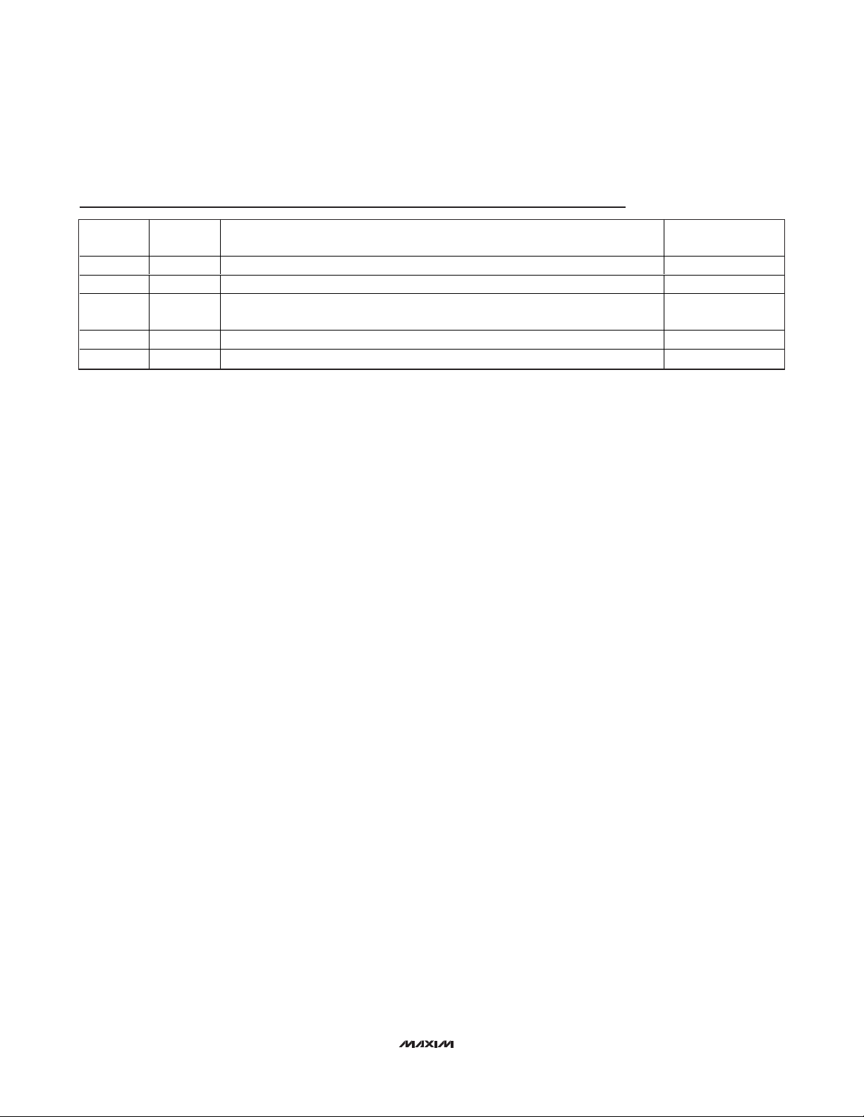
MAX9775/MAX9776
2 x 1.5W, Stereo Class D Audio Subsystem
with DirectDrive Headphone Amplifier
Maxim cannot assume responsibility for use of any circuitry other than circuitry entirely embodied in a Maxim product. No circuit patent licenses are
implied. Maxim reserves the right to change the circuitry and specifications without notice at any time.
38
____________________Maxim Integrated Products, 120 San Gabriel Drive, Sunnyvale, CA 94086 408-737-7600
© 2008 Maxim Integrated Products is a registered trademark of Maxim Integrated Products, Inc.
Revision History
REVISION
NUMBER
0 3/07 Initial release —
1 7/07 Initial release of MAX9776 UCSP package and updated Tables 3 and 5b 1, 7, 27, 28
2 9/07
3 1/08 Updated the Typical Application Circuits 17, 18
4 8/08 Changed package code and drawing 1, 33, 34, 37
REVISION
DATE
DESCRIPTION
Initial release of MAX9775 UCSP and removal of MAX9775 TQFN, updated Pin
Description and Table 9
PAGES
CHANGED
1, 12, 15, 30, 33, 34
 Loading...