

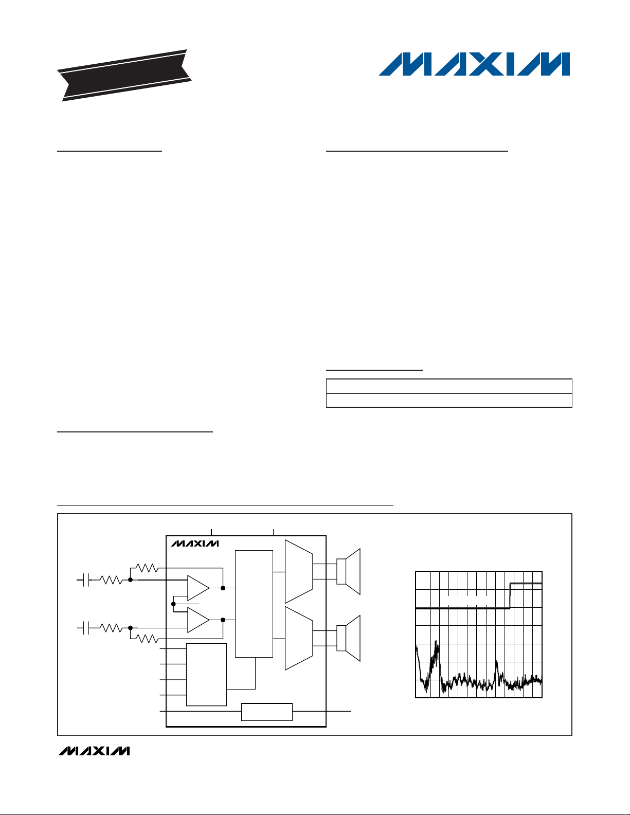
General Description
The MAX9744 20W stereo Class D audio power amplifier provides Class AB amplifier performance with Class
D efficiency, conserving board space and eliminating
the need for a bulky heatsink. This device features single-supply operation, adjustable gain, shutdown mode,
a SYNC output, speaker mute, and industry-leading
click-and-pop suppression.
The MAX9744 features a 64-step dual-mode (analog or
digital), programmable volume control and mute function. The MAX9744 operates from a 4.5V to 14V single
supply and can deliver up to 20W per channel into a
4Ω speaker with a 14V supply.
The MAX9744 offers two modulation schemes: a fixedfrequency modulation mode that allows one of several
preset switching frequencies to be selected, and a
spread-spectrum modulation mode that helps to
reduce EMI-radiated emissions.
The MAX9744 features high 75dB PSRR, low 0.04%
THD+N, and SNR in excess of 90dB. Robust short-circuit and thermal-overload protection prevent device
damage during a fault condition. The MAX9744 is available in a 44-pin thin QFN-EP (7mm x 7mm x 0.8mm)
package and is specified over the extended -40°C to
+85°C temperature range.
Applications
Flat-Panel Televisions
PC Speaker Systems
Multimedia Docking Stations
Features
♦ Wide 4.5V to 14V Power-Supply Voltage Range
♦ Filterless Spread-Spectrum Modulation Lowers
Radiated RF Emissions from Speaker Cables
♦ 20W Stereo Output (4Ω, VDD= 12V, THD+N = 10%)
♦ Integrated Volume Control (I2C or Analog)
♦ Low 0.04% THD+N
♦ High 75dB PSRR
♦ High 93% Efficiency
♦ Integrated Click-and-Pop Suppression
♦ Low-Power Shutdown Mode
♦ Short-Circuit and Thermal-Overload Protection
♦ Available in a 44-Pin Thin QFN-EP (7mm x 7mm x
0.8mm)
MAX9744
20W Stereo Class D Speaker Amplifier
with Volume Control
________________________________________________________________
Maxim Integrated Products
1
19-4078; Rev 1; 9/08
For pricing, delivery, and ordering information, please contact Maxim Direct at 1-888-629-4642,
or visit Maxim’s website at www.maxim-ic.com.
Pin Configuration appears at end of data sheet.
EVALUATION KIT
AVAILABLE
MAX9744
BIAS
SYNCOUTSYNC
VOLUME
CONTROL
CLASS D
MODULATOR
CLASS D
MODULATOR
MUTE
SHUTDOWN
CONTROL
I
2
C
ANALOG
CONTROL
OSCILLATOR
3V TO 3.6V 4.5V TO 14V
MAX9744 EMI WITH FERRITE BEAD FILTERS
(V
DD
= 12V, 1m CABLE, 8Ω LOAD)
FREQUENCY (MHz)
220
200
60
80
100
140
160
120
180
5
10
15
20
25
30
35
40
30
240
260
280
300
OUTPUT MAGNITUDE (dBV)
EN5022 B LIMIT
Simplified Block Diagram
+
Denotes a lead-free/RoHS-compliant package.
*
EP = Exposed pad.
PART TEMP RANGE PIN-PACKAGE
MAX9744ETH+ -40°C to +85°C 44 TQFN-EP*
Ordering Information
MAX9744
20W Stereo Class D Speaker Amplifier
with Volume Control
2 _______________________________________________________________________________________
ABSOLUTE MAXIMUM RATINGS
ELECTRICAL CHARACTERISTICS
(V
PVDD
= 12V, V
DD
= 3.3V, V
GND
= V
PGND
= 0V, V
MUTE
= 0V; max volume setting; all speaker load resistors connected between
OUT_+ and OUT_-, R
L
= ∞, unless otherwise stated, C
BOOT_
= 0.1µF, C
BIAS
= 2.2µF, CIN= 0.47µF, RIN= 20kΩ, RF_= 20kΩ, spread-
spectrum mode, filterless modulation mode, see the
Functional Diagrams/Typical Application Circuits.
TA= T
MIN
to T
MAX
, unless oth-
erwise noted. Typical values are at T
A
= +25°C.) (Note 1)
Stresses beyond those listed under “Absolute Maximum Ratings” may cause permanent damage to the device. These are stress ratings only, and functional
operation of the device at these or any other conditions beyond those indicated in the operational sections of the specifications is not implied. Exposure to
absolute maximum rating conditions for extended periods may affect device reliability.
PVDD to PGND ....................................................................+16V
V
DD
to GND ...........................................................................+4V
FB_, SYNCOUT, SYNC, SDA/VOL, ADDR1,
ADDR2 to GND........................................-0.3V to (V
DD
+ 0.3V)
BOOT_ to V
DD
..........................................................-0.3V to +6V
BOOT_ to OUT_........................................................-0.3V to +6V
OUT_ to GND ..........................................-0.3V to (PVDD + 0.3V)
PGND to GND .......................................................-0.3V to +0.3V
Any Other Pin to GND ..............................................-0.3V to +4V
OUT_, Short-Circuit Duration......................................Continuous
Continuous Power Dissipation (T
A
= +70°C)
44-Pin Thin QFN (derate 27mW/°C above +70°C,
single-layer board) ...................................................2162mW
44-Pin Thin QFN (derate 37mW/°C above +70°C,
multilayer board) ......................................................2963mW
θ
JA
, Single-Layer Board................................................37°C/W
θ
JA
, Multilayer Board ................................................….27°C/W
Continuous Input Current (PVDD, PGND).............................6.4A
Continuous Output Current (OUT_) ......................................3.2A
Continuous Input Current (except OUT_).........................±20mA
Junction Temperature......................................................+150°C
Operating Temperature Range ...........................-40°C to +85°C
Storage Temperature Range .............................-65°C to +150°C
Lead Temperature (soldering, 10s) .................................+300°C
PARAMETER SYMBOL CONDITIONS MIN TYP MAX UNITS
GENERAL
Speaker Amplifier Supply Voltage
Range
Supply Voltage Range V
Quiescent Current
Shutdown Current
Turn-On Time t
Common-Mode Bias Voltage V
Input Amplifier Output-Voltage
Swing High
Input Amplifier Output-Voltage
Swing Low
Input Amplifier Output ShortCircuit Current Limit
Input Amplifier Gain-Bandwidth
Product
SPEAKER AMPLIFIERS
Gain A
Output Offset V
I
VDDSHDNTA
I
PVDDSHDNTA
PVDD Inferred from PSRR test 4.5 14 V
I
DD
I
DD
PVDD
ON
BIAS
V
OH
V
OL
GBW 1.8 MHz
VMAX
OS
Inferred from PSRR test 2.7 3.6 V
= +25°C 0.1 1
= +25°C 0.1 1
Specified as VDD – VOH, RL = 2kΩ
connected to 1.5V
Specified as VOL – GND, RL = 2kΩ
connected to 1.5V
Maximum
volume setting
TA = 25°C ±2 ±15 mV
Output stage gain 29.5
Total gain (Note 2) 29.5
20 35
10 20
200 ms
1.5 V
20 mV
20 mV
±60 mA
mA
µA
dB
MAX9744
20W Stereo Class D Speaker Amplifier
with Volume Control
_______________________________________________________________________________________ 3
ELECTRICAL CHARACTERISTICS (continued)
(V
PVDD
= 12V, V
DD
= 3.3V, V
GND
= V
PGND
= 0V, V
MUTE
= 0V; max volume setting; all speaker load resistors connected between
OUT_+ and OUT_-, R
L
= ∞, unless otherwise stated, C
BOOT_
= 0.1µF, C
BIAS
= 2.2µF, CIN= 0.47µF, RIN= 20kΩ, RF_= 20kΩ, spread-
spectrum mode, filterless modulation mode, see the
Functional Diagrams/Typical Application Circuits.
TA= T
MIN
to T
MAX
, unless oth-
erwise noted. Typical values are at T
A
= +25°C.) (Note 1)
PARAMETER SYMBOL CONDITIONS MIN TYP MAX UNITS
Efficiency (Note 3)
Output Power P
Hard Output Current Limit I
Total Harmonic Distortion Plus
Noise
η
OUT
SC
THD+N
Signal-to-Noise Ratio SNR
Filterless
modulation
PWM
V
= 5V,
PVDD
f
= 1kHz
IN
V
= 12V,
PVDD
= 1kHz
f
IN
V
= 14V,
PVDD
= 1kHz
f
IN
f = 1kHz, R
8Ω, P
= 1kHz
f
IN
P
OUT
R
= 8Ω,
L
= 5W,
OUT
= 10W,
=
L
filterless
modulation
mode, BW =
22Hz to 22kHz
= 10W,
P
OUT
= 8Ω, PWM
R
L
mode, BW =
22Hz to 22kHz
P
= 10W, fIN = 1kHz,
OUT
8Ω load
P
= 15W, fIN = 1kHz,
OUT
4Ω load
P
= 10W, fIN = 1kHz,
OUT
8Ω load
P
= 15W, f
OUT
4Ω load
= 1kHz,
IN
93
87
92
88
RL = 8Ω, THD+N = 1% 1.4
RL = 8Ω, THD+N = 10% 1.8
RL = 4Ω, THD+N = 1% 2.6
R
= 4Ω, THD+N = 10% 3.6
L
RL = 8Ω, THD+N = 1% 8
RL = 8Ω, THD+N = 10% 10
RL = 4Ω, THD+N = 1% 14
R
= 4Ω, THD+N = 10% 17
L
RL = 8Ω, THD+N = 1% 10
RL = 8Ω, THD+N = 10% 13
RL = 4Ω, THD+N = 1% 17.5
R
= 4Ω, THD+N = 10% 22.5
L
3.9 5.5 A
Filterless modulation 0.04
PWM 0.04
Fixed-frequency
modulation, unweighted
Spread-spectrum,
unweighted
Fixed-frequency
modulation, A-weighted
Spread-spectrum,
A-weighted
Fixed-frequency
modulation, unweighted
Spread-spectrum,
unweighted
Fixed-frequency
modulation, A-weighted
Spread-spectrum,
A-weighted
91
90
94
94
91
81
94
89
%
%
W
%
dB
dB
MAX9744
20W Stereo Class D Speaker Amplifier
with Volume Control
4 _______________________________________________________________________________________
ELECTRICAL CHARACTERISTICS (continued)
(V
PVDD
= 12V, V
DD
= 3.3V, V
GND
= V
PGND
= 0V, V
MUTE
= 0V; max volume setting; all speaker load resistors connected between
OUT_+ and OUT_-, R
L
= ∞, unless otherwise stated, C
BOOT_
= 0.1µF, C
BIAS
= 2.2µF, CIN= 0.47µF, RIN= 20kΩ, RF_= 20kΩ, spread-
spectrum mode, filterless modulation mode, see the
Functional Diagrams/Typical Application Circuits.
TA= T
MIN
to T
MAX
, unless oth-
erwise noted. Typical values are at T
A
= +25°C.) (Note 1)
PARAMETER SYMBOL CONDITIONS MIN TYP MAX UNITS
Crosstalk
Power-Supply Rejection Ratio PSRR
SYNC Frequency f
Class D Switching Frequency f
SYNC Frequency Lock Range 1000 1600 kHz
Minimum SYNC Frequency Lock
Duty Cycle
Maximum SYNC Frequency Lock
Duty Cycle
Gain Matching Full volume (ideal matching for R
Click-and-Pop Level K
VOLUME CONTROL
VOL Input Leakage Current ±5 µA
Input Hysteresis DC volume control mode 11 mV
9.5dB Gain Voltage DC volume control mode 0.1 x V
Full Mute Voltage DC volume control mode 0.9 x V
Full Mute Attenuation f = 1kHz, relative to 9.5dB setting -115 dB
DIGITAL INPUTS/OUTPUT (SHDN, MUTE, ADDR1, ADDR2, SCLK, SDA/VOL)
Input-Voltage High V
Input-Voltage Low V
Input Leakage Current I
Input Hysteresis SCLK, SDA/VOL 0.1 x V
Input Capacitance C
Output-Voltage Low V
SYNC
SW
CP
IH
IL
LK
IN
IL
1kHz 85
20Hz to 20kHz 68
VDD = 2.7V to 3.6V, TA = 25°C,
MUTE = high
PVDD = 4.5V to 14V 50 83
f = 1kHz, V
f = 1kHz, V
SYNC = GND 1020 1200 1355
SYNC = unconnected 1280 1440 1640
SYNC = VDD (spread-spectrum mode)
SYNC = GND 255 300 338
SYNC = unconnected 320 360 410
SYNC = VDD (spread-spectrum mode)
Peak voltage, 32
samples/second,
A-weighted (Note 4)
TA = +25°C ±1 µA
IOL = 3mA 0.4 V
= 100mV
RIPPLE
= 200mV
RIPPLE
on V
P-P
P-P
Into shutdown -43
Out of shutdown -43
Into mute -46
Out of mute -57
DD
on PVDD 75
and RF) 0.2 dB
IN
0.7 x V
DD
68
70
1200
±30
300
±6
40 %
60 %
DD
DD
0.3 x V
DD
5pF
DD
dB
dB
kHz
kHz
dBV
V
V
V
V
V
MAX9744
20W Stereo Class D Speaker Amplifier
with Volume Control
_______________________________________________________________________________________ 5
ELECTRICAL CHARACTERISTICS (continued)
(V
PVDD
= 12V, V
DD
= 3.3V, V
GND
= V
PGND
= 0V, V
MUTE
= 0V; max volume setting; all speaker load resistors connected between
OUT_+ and OUT_-, R
L
= ∞, unless otherwise stated, C
BOOT_
= 0.1µF, C
BIAS
= 2.2µF, CIN= 0.47µF, RIN= 20kΩ, RF_= 20kΩ, spread-
spectrum mode, filterless modulation mode, see the
Functional Diagrams/Typical Application Circuits.
TA= T
MIN
to T
MAX
, unless oth-
erwise noted. Typical values are at T
A
= +25°C.) (Note 1)
Note 1: All devices are 100% production tested at +25°C. All temperature limits are guaranteed by design.
Note 2: See the
Gain-Setting Resistors
section.
Note 3: Measured on the MAX9744 Evaluation Kit.
Note 4: Testing performed with an 8Ω resistive load connected across BTL output. Mode transitions are controlled by SHDN or
MUTE pin, respectively.
Note 5: A master device must provide a hold time of at least 300ns for the SDA signal in order to bridge the undefined region of the
SCL’s falling edge.
Note 6: C
B
= total capacitance of one bus line in pF.
PARAMETER SYMBOL CONDITIONS MIN TYP MAX UNITS
DIGITAL INPUT (SYNC)
Input-Voltage High V
Input-Voltage Low V
SYNC Input Leakage I
SYNCIH
SYNCIL
SYNCIN
TA = +25°C ±7.5 ±13 µA
2.3 V
0.8 V
DIGITAL OUTPUT (SYNCOUT)
-
V
Output-Voltage High V
Output-Voltage Low V
SYNCOUTIH
SYNCOUTILISINK
I
SOURCE
= 1mA
= 1mA 0.3 V
DD
0.3
Rise/Fall Time CL = 10pF 50 V/µs
THERMAL PROTECTION
Thermal-Shutdown Threshold +165 °C
Thermal-Shutdown Hysteresis 15 °C
I2C TIMING CHARACTERISTICS (Figure 3)
Serial Clock f
Bus Free Time Between a STOP
and a START Condition
Hold Time (Repeated) START
Condition
Repeated START Condition
Setup Time
STOP Condition Setup Time t
Data Hold Time t
Data Setup Time t
t
HD, STA
t
SU, STA
SU, STO
HD,DAT
SU,DAT
SCL Clock Low Period t
SCL Clock High Period t
Rise Time of SDA and SCL,
Receiving
Fall Time of SDA and SCL,
Receiving
Pulse Width of Spike Suppressed t
Capacitive Load for Each Bus
Line
SCL
t
BUF
LOW
HIGH
t
R
t
F
SP
C
B
1.3 µs
(Note 5) 0.6 µs
0.6 µs
0.6 µs
0 0.9 µs
100 ns
1.3 µs
0.6 µs
(Note 6)
(Note 6)
20 +
0.1C
20 +
0.1C
B
B
050ns
400 kHz
300 ns
300 ns
400 pF
V
MAX9744
20W Stereo Class D Speaker Amplifier
with Volume Control
6 _______________________________________________________________________________________
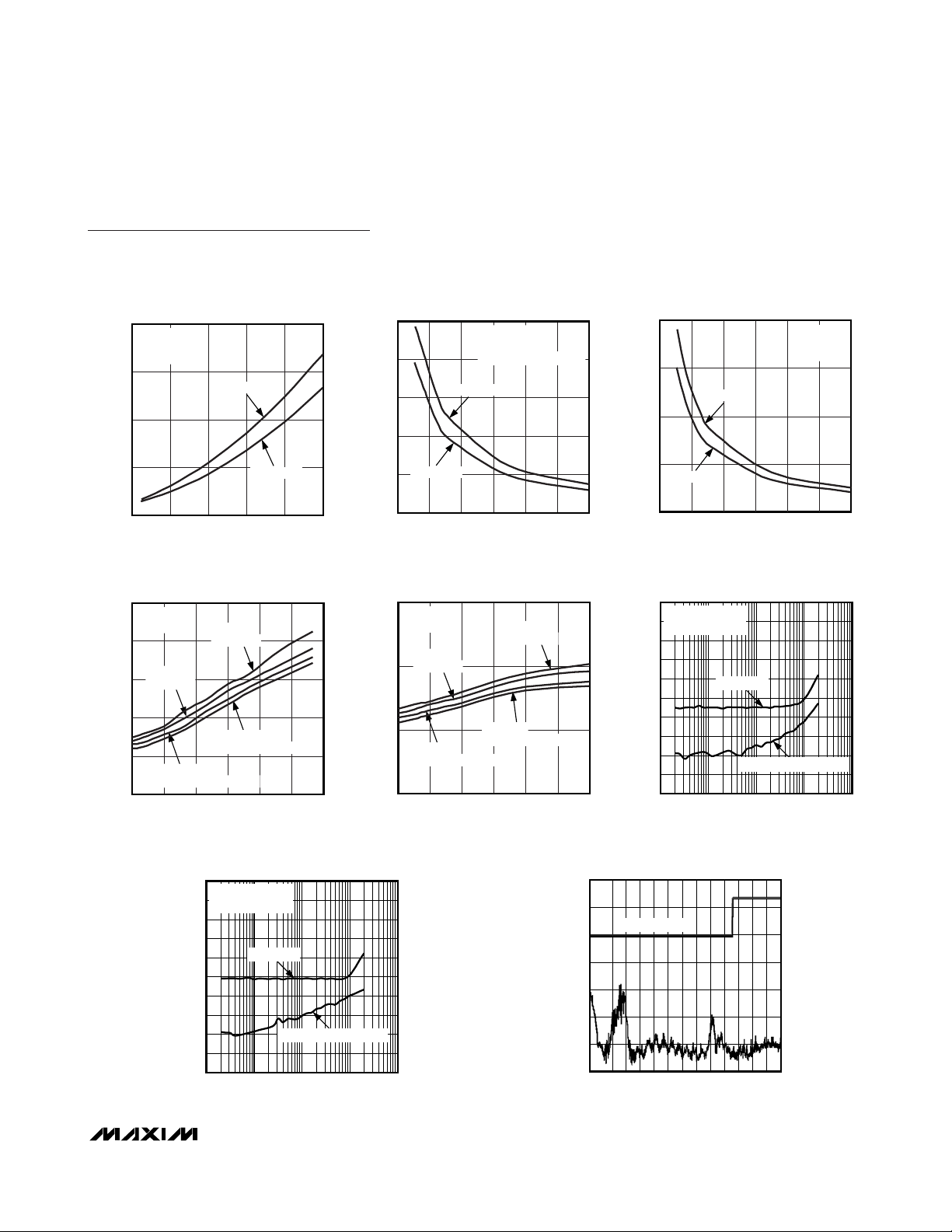
Typical Operating Characteristics
(V
PVDD
= 12V, VDD= 3.3V, V
GND
= V
PGND
= 0V, V
MUTE
= 0V; max volume setting; all speaker load resistors connected between
OUT_+ and OUT_- with an inductor in series, 8Ω load, L = 68µH, 4Ω load, L= 33µH. R
L
= ∞, unless otherwise stated, C
BIAS
= 2.2µF,
C
IN
= 0.47µF, RIN= 20kΩ, RF_= 20kΩ, spread-spectrum mode, TA= +25°C, unless otherwise noted.)
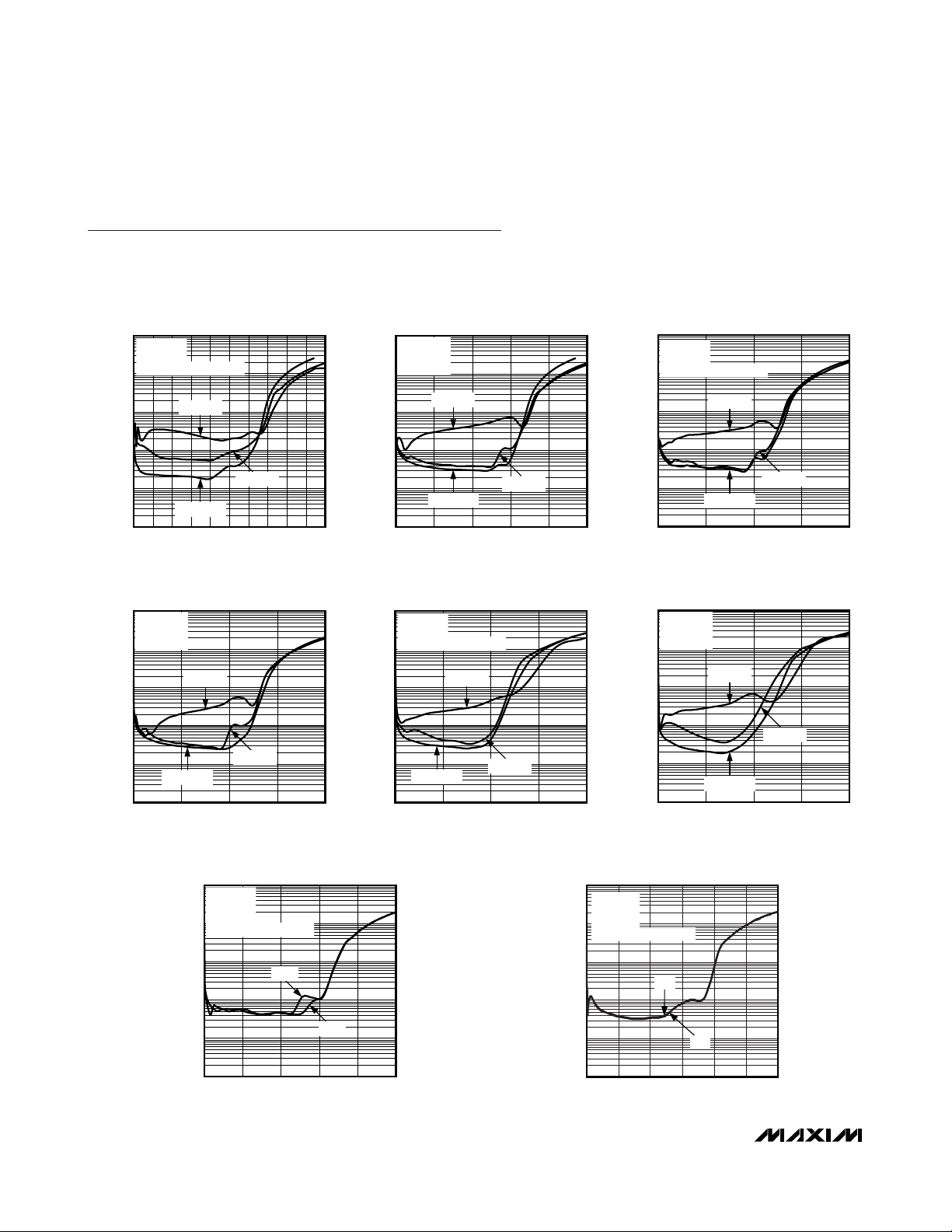
TOTAL HARMONIC DISTORTION PLUS NOISE
vs. OUTPUT POWER
MAX9744 toc01
OUTPUT POWER (W)
THD+N (%)
18161412108642
0.01
0.1
1
10
100
0.001
020
fIN = 6kHz
fIN = 100Hz
fIN = 1kHz
PVDD = 12V
R
L
= 4Ω
FILTERLESS MODULATION
TOTAL HARMONIC DISTORTION PLUS NOISE
vs. OUTPUT POWER
MAX9744 toc02
OUTPUT POWER (W)
THD+N (%)
161284
0.01
0.1
1
10
100
0.001
020
PVDD = 12V
R
L
= 4Ω
PWM MODE
fIN = 6kHz
fIN = 100Hz
fIN = 1kHz
TOTAL HARMONIC DISTORTION PLUS NOISE
vs. OUTPUT POWER
MAX9744 toc03
OUTPUT POWER (W)
THD+N (%)
963
0.01
0.1
1
10
100
0.001
012
PVDD = 12V
R
L
= 8Ω
FILTERLESS MODULATION
fIN = 6kHz
fIN = 100Hz
fIN = 1kHz
TOTAL HARMONIC DISTORTION PLUS NOISE
vs. OUTPUT POWER
MAX9744 toc04
OUTPUT POWER (W)
THD+N (%)
963
0.01
0.1
1
10
100
0.001
012
PVDD = 12V
R
L
= 8Ω
PWM MODE
fIN = 6kHz
fIN = 100Hz
fIN = 1kHz
TOTAL HARMONIC DISTORTION PLUS NOISE
vs. OUTPUT POWER
MAX9744 toc05
OUTPUT POWER (W)
THD+N (%)
321
0.01
0.1
1
10
100
0.001
04
fIN = 6kHz
fIN = 100Hz
fIN = 1kHz
PVDD = 5V
R
L
= 4Ω
FILTERLESS MODULATION
TOTAL HARMONIC DISTORTION PLUS NOISE
vs. OUTPUT POWER
MAX9744 toc06
OUTPUT POWER (W)
THD+N (%)
321
0.01
0.1
1
10
100
0.001
04
PVDD = 5V
R
L
= 4Ω
PWM MODE
fIN = 6kHz
fIN = 100Hz
fIN = 1kHz
TOTAL HARMONIC DISTORTION PLUS NOISE
vs. OUTPUT POWER
MAX9744 toc08
OUTPUT POWER (W)
THD+N (%)
106842
0.01
0.1
1
10
100
0.001
012
PVDD = 12V
R
L
= 8Ω
f
IN
= 1kHz
FILTERLESS MODULATION
SSM
FFM
TOTAL HARMONIC DISTORTION PLUS NOISE
vs. OUTPUT POWER
MAX9744 toc07
OUTPUT POWER (W)
THD+N (%)
161284
0.01
0.1
1
10
100
0.001
020
PVDD = 12V
R
L
= 4Ω
f
IN
= 1kHz
FILTERLESS MODULATION
FFM
SSM
MAX9744
20W Stereo Class D Speaker Amplifier
with Volume Control
_______________________________________________________________________________________
7
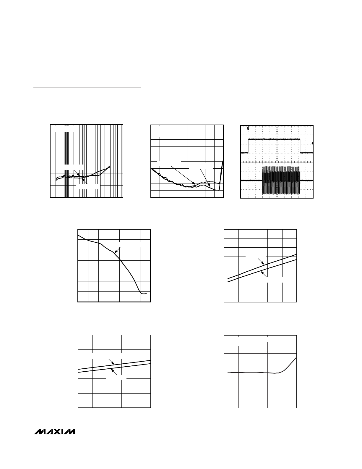
Typical Operating Characteristics (continued)
(V
PVDD
= 12V, VDD= 3.3V, V
GND
= V
PGND
= 0V, V
MUTE
= 0V; max volume setting; all speaker load resistors connected between
OUT_+ and OUT_- with an inductor in series, 8Ω load, L = 68µH, 4Ω load, L= 33µH. R
L
= ∞, unless otherwise stated, C
BIAS
= 2.2µF,
C
IN
= 0.47µF, RIN= 20kΩ, RF_= 20kΩ, spread-spectrum mode, TA= +25°C, unless otherwise noted.)
TOTAL HARMONIC DISTORTION PLUS NOISE
vs. OUTPUT POWER
100
PVDD = 12V
= 4Ω
R
L
= 1kHz
f
IN
10
PWM MODE
1
THD+N (%)
0.1
0.01
0.001
020
FFM
SSM
OUTPUT POWER (W)
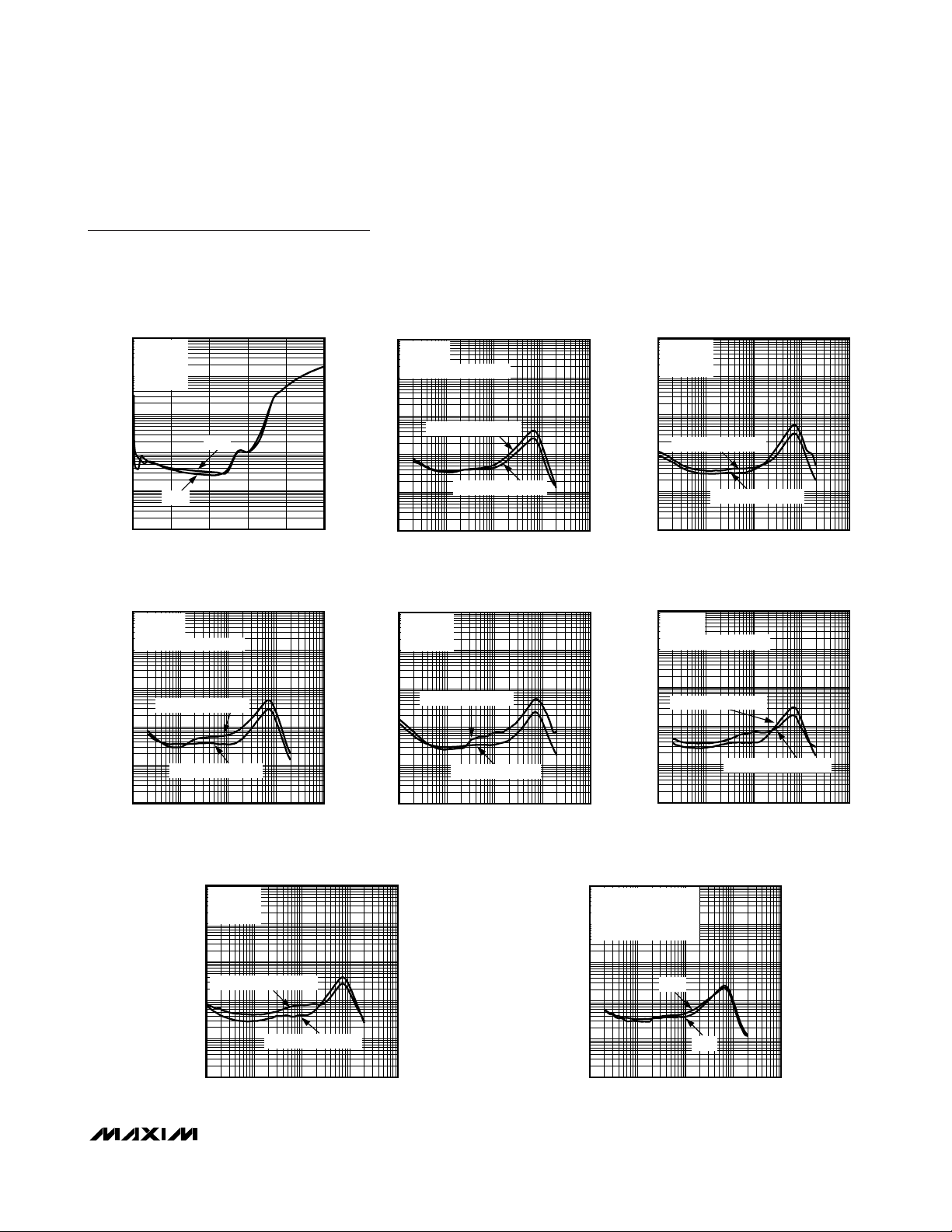
TOTAL HARMONIC DISTORTION PLUS NOISE
vs. FREQUENCY
100
PVDD = 12V
= 8Ω
R
L
FILTERLESS MODULATION
10
161284
MAX9744 toc09
MAX9744 toc12
TOTAL HARMONIC DISTORTION PLUS NOISE
vs. FREQUENCY
100
PVDD = 12V
= 4Ω
R
L
FILTERLESS MODULATION
10
1
OUTPUT POWER = 10W
THD+N (%)
0.1
0.01
0.001
10 100k
OUTPUT POWER = 5W
10k1k100
FREQUENCY (Hz)
TOTAL HARMONIC DISTORTION PLUS NOISE
vs. FREQUENCY
100
PVDD = 12V
= 8Ω
R
L
PWM MODE
10
MAX9744 toc10
MAX9744 toc13
TOTAL HARMONIC DISTORTION PLUS NOISE
vs. FREQUENCY
100
PVDD = 12V
= 4Ω
R
L
PWM MODE
10
1
THD+N (%)
0.001
OUTPUT POWER = 10W
0.1
0.01
10 100k
OUTPUT POWER = 5W
10k1k100
FREQUENCY (Hz)
TOTAL HARMONIC DISTORTION PLUS NOISE
vs. FREQUENCY
100
PVDD = 5V
= 4Ω
R
L
FILTERLESS MODULATION
10
MAX9744 toc11
MAX9744 toc14
1
OUTPUT POWER = 6W
THD+N (%)
0.1
0.01
0.001
OUTPUT POWER = 3W
10 100k
FREQUENCY (Hz)
TOTAL HARMONIC DISTORTION PLUS NOISE
vs. FREQUENCY
100
PVDD = 5V
= 4Ω
R
L
PWM MODE
10
1
OUTPUT POWER = 500mW
THD+N (%)
0.1
0.01
0.001
10 100k
10k1k100
OUTPUT POWER = 1.5W
10k1k100
FREQUENCY (Hz)
1
OUTPUT POWER = 6W
THD+N (%)
0.1
0.01
0.001
10 100k
MAX9744 toc15
OUTPUT POWER = 3W
FREQUENCY (Hz)
1
OUTPUT POWER = 1.5W
THD+N (%)
0.1
0.01
0.001
10k1k100
10 100k
TOTAL HARMONIC DISTORTION PLUS NOISE
vs. FREQUENCY
100
PVDD = 12V
= 4Ω
R
L
FILTERLESS MODULATION
10
= 5W
P
OUT
1
THD+N (%)
0.1
0.01
0.001
10 100k
SSM
FREQUENCY (Hz)
OUTPUT POWER = 500mW
10k1k100
FREQUENCY (Hz)
MAX9744 toc16
FFM
10k1k100
MAX9744
20W Stereo Class D Speaker Amplifier
with Volume Control
8 _______________________________________________________________________________________
Typical Operating Characteristics (continued)
(V
PVDD
= 12V, VDD= 3.3V, V
GND
= V
PGND
= 0V, V
MUTE
= 0V; max volume setting; all speaker load resistors connected between
OUT_+ and OUT_- with an inductor in series, 8Ω load, L = 68µH, 4Ω load, L= 33µH. R
L
= ∞, unless otherwise stated, C
BIAS
= 2.2µF,
C
IN
= 0.47µF, RIN= 20kΩ, RF_= 20kΩ, spread-spectrum mode, TA= +25°C, unless otherwise noted.)
TOTAL HARMONIC DISTORTION PLUS NOISE
vs. FREQUENCY
MAX9744 toc17
FREQUENCY (Hz)
THD+N (%)
10k1k100
0.01
0.1
1
10
100
0.001
10 100k
PVDD = 12V
R
L
= 8Ω
FILTERLESS MODULATION
P
OUT
= 3W
FFM
SSM
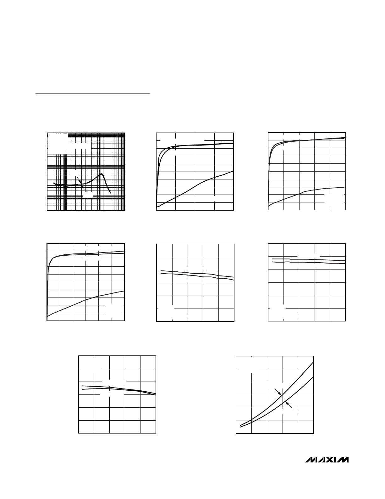
EFFICIENCY vs. OUTPUT POWER
MAX9744 toc18
OUTPUT POWER (W)
EFFICIENCY (%)
POWER DISSIPATION (mW)
1284
10
20
30
40
50
60
70
80
90
100
0
1
2
3
4
5
6
7
8
9
10
0
016
PVDD = 12V, fIN = 1kHz, RL = 4Ω
FILTERLESS MODULATION
PWM MODE
EFFICIENCY vs. OUTPUT POWER
MAX9744 toc19
OUTPUT POWER (W)
(PER CHANNEL)
EFFICIENCY (%)
POWER DISSIPATION
10624
20
10
40
60
80
30
50
70
90
100
0
5W
0W
08
PWM MODE
FILTERLESS MODULATION
PVDD = 12V
f
IN
= 1kHz
R
L
= 8Ω
EFFICIENCY vs. OUTPUT POWER
MAX9744 toc20
OUTPUT POWER (W)
EFFICIENCY (%)
POWER DISSIPATION
3.01.50.5 1.0
20
10
40
60
80
30
50
70
90
100
0
2W
0W
0 2.0 2.5
PWM MODE
FILTERLESS MODULATION
PVDD = 5V
f
IN
= 1kHz
R
L
= 4Ω
EFFICIENCY vs. SUPPLY VOLTAGE
MAX9744 toc21
SUPPLY VOLTAGE (V)
EFFICIENCY (%)
141068
75
80
85
90
95
100
70
412
fIN = 1kHz
R
L
= 4Ω
FILTERLESS MODULATION
THD+N = 10%
THD+N = 1%
EFFICIENCY vs. SUPPLY VOLTAGE
MAX9744 toc22
SUPPLY VOLTAGE (V)
EFFICIENCY (%)
141068
75
80
85
90
95
100
70
412
fIN = 1kHz
R
L
= 8Ω
FILTERLESS MODULATION
THD+N = 10%
THD+N = 1%
OUTPUT POWER vs. SUPPLY VOLTAGE
MAX9744 toc24
SUPPLY VOLTAGE (V)
OUTPUT POWER (W)
121086
4
8
12
16
20
24
0
414
fIN = 1kHz
R
L
= 4Ω
PWM MODE
THD+N = 10%
THD+N = 1%
EFFICIENCY vs. SUPPLY VOLTAGE
MAX9744 toc23
SUPPLY VOLTAGE (V)
EFFICIENCY (%)
121086
75
80
85
90
95
100
70
414
fIN = 1kHz
R
L
= 4Ω
PWM MODE
THD+N = 10%
THD+N = 1%
MAX9744
20W Stereo Class D Speaker Amplifier
with Volume Control
_______________________________________________________________________________________
9
Typical Operating Characteristics (continued)
(V
PVDD
= 12V, VDD= 3.3V, V
GND
= V
PGND
= 0V, V
MUTE
= 0V; max volume setting; all speaker load resistors connected between
OUT_+ and OUT_- with an inductor in series, 8Ω load, L = 68µH, 4Ω load, L= 33µH. R
L
= ∞, unless otherwise stated, C
BIAS
= 2.2µF,
C
IN
= 0.47µF, RIN= 20kΩ, RF_= 20kΩ, spread-spectrum mode, TA= +25°C, unless otherwise noted.)
OUTPUT POWER vs. SUPPLY VOLTAGE
MAX9744 toc25
SUPPLY VOLTAGE (V)
OUTPUT POWER (W)
141068
4
8
12
16
0
412
RL = 8Ω
f
IN
= 1kHz
PWM MODE
THD+N = 10%
THD+N = 1%
OUTPUT POWER vs. LOAD RESISTANCE
MAX9744 toc26
LOAD RESISTANCE (Ω)
OUTPUT POWER (W)
3015510
4
8
12
20
16
0
02520
PVDD = 12V
f = 1kHz
FILTERLESS MODULATION
THD+N = 10%
THD+N = 1%
OUTPUT POWER vs. LOAD RESISTANCE
MAX9744 toc27
LOAD RESISTANCE (Ω)
OUTPUT POWER (W)
3015510
1
2
4
3
0
02520
PVDD = 5V
f = 1kHz
PWM MODE
THD+N = 10%
THD+N = 1%
CASE TEMPERATURE
vs. OUTPUT POWER
MAX9744 toc28
OUTPUT POWER (W)
CASE TEMPERATURE (°C)
18936
25
50
125
100
75
0
01512
fIN = 1kHz
R
L
= 4Ω
PVDD = 14V
PWM MODE
PVDD = 12V
PWM MODE
PVDD = 14V
FILTERLESS MODULATION
PVDD = 12V
FILTERLESS MODULATION
CASE TEMPERATURE
vs. OUTPUT POWER
MAX9744 toc29
OUTPUT POWER (W)
CASE TEMPERATURE (°C)
12624
25
75
50
0
0108
fIN = 1kHz
R
L
= 8Ω
PVDD = 12V
PWM MODE
PVDD = 14V
PWM MODE
PVDD = 14V
FILTERLESS MODULATION
PVDD = 12V
FILTERLESS MODULATION
POWER-SUPPLY REJECTION RATIO (PVDD)
vs. FREQUENCY
MAX9744 toc30
FREQUENCY (Hz)
PSRR (dB)
10k1k100
-90
-80
-70
-60
-50
-40
-30
-20
-10
0
-100
10 100k
PWM MODE
FILTERLESS MODULATION
PVDD = 12V
V
RIPPLE
= 200mV
P-P
EMI WITH FERRITE BEAD FILTERS
(V
DD
= 12V, 1m CABLE, 8Ω LOAD)
MAX9744 toc32
OUTPUT MAGNITUDE (dBV)
5
10
15
20
25
30
35
40
FREQUENCY (MHz)
220
200
60
80
100
140
160
120
180
30
240
260
280
300
EN5022 B LIMIT
POWER-SUPPLY REJECTION RATIO (VDD)
vs. FREQUENCY
MAX9744 toc31
FREQUENCY (Hz)
PSRR (dB)
10k1k100
-90
-80
-70
-60
-50
-40
-30
-20
-10
0
-100
10 100k
PWM MODE
FILTERLESS MODULATION
VDD = 3.3V
V
RIPPLE
= 100mV
P-P

MAX9744
20W Stereo Class D Speaker Amplifier
with Volume Control
10 ______________________________________________________________________________________
OUTPUT
MAGNITUDE
(dBV)
Typical Operating Characteristics (continued)
(V
PVDD
= 12V, VDD= 3.3V, V
GND
= V
PGND
= 0V, V
MUTE
= 0V; max volume setting; all speaker load resistors connected between
OUT_+ and OUT_- with an inductor in series, 8Ω load, L = 68µH, 4Ω load, L= 33µH. R
L
= ∞, unless otherwise stated, C
BIAS
= 2.2µF,
C
IN
= 0.47µF, RIN= 20kΩ, RF_= 20kΩ, spread-spectrum mode, TA= +25°C, unless otherwise noted.)
OUTPUT WAVEFORM
(FILTERLESS MODULATION)
MAX9744 toc33
2V/div
OUTPUT WAVEFORM (PWM)
MAX9744 toc34
0
2V/div
-20
-40
-60
-80
OUTPUT FREQUENCY SPECTRUM
FFM MODE
= -60dBV
V
IN
f = 1kHz
= 4Ω
R
L
UNWEIGHTED
LEFT
MAX9744 toc35
2V/div
1μs/div
WIDEBAND OUTPUT SPECTRUM
OUTPUT FREQUENCY SPECTRUM
0
-20
-40
-60
-80
-100
-120
-140
020
RIGHT
FREQUENCY (kHz)
LEFT
SSM MODE
= -60dBV
V
IN
f = 1kHz
= 4Ω
R
L
UNWEIGHTED
15105
MAX9744 toc36
(FIXED-FREQUENCY MODULATION MODE)
20
RBW = 1kHz
INPUT AC GROUNDED
0
FILTERLESS MODULATION
-20
-40
-60
-80
OUTPUT AMPLITUDE (dBV)
-100
-120
0 100
WIDEBAND OUTPUT SPECTRUM
(SPREAD-SPECTRUM MODULATION MODE)
20
RBW = 1kHz
INPUT AC GROUNDED
0
FILTERLESS MODULATION
-20
MAX9744 toc39
1μs/div
FREQUENCY (MHz)
2V/div
-100
OUTPUT MAGNITUDE (dBV)
-120
-140
020
RIGHT
15105
FREQUENCY (kHz)
WIDEBAND OUTPUT SPECTRUM
(FIXED-FREQUENCY MODULATION MODE)
20
RBW = 1kHz
INPUT AC GROUNDED
0
MAX9744 toc37
101
PWM MODE
-20
-40
-60
-80
OUTPUT AMPLITUDE (dBV)
-100
-120
0 100
FREQUENCY (MHz)
101
MAX9744 toc38
WIDEBAND OUTPUT SPECTRUM
(SPREAD-SPECTRUM MODULATION MODE)
20
RBW = 1kHz
INPUT AC GROUNDED
0
PWM MODE
-20
MAX9744 toc40
-40
-60
-80
OUTPUT AMPLITUDE (dBV)
-100
-120
0 100
FREQUENCY (MHz)
101
-40
-60
-80
OUTPUT AMPLITUDE (dBV)
-100
-120
0 100
FREQUENCY (MHz)
101
MAX9744
20W Stereo Class D Speaker Amplifier
with Volume Control
______________________________________________________________________________________
11
Typical Operating Characteristics (continued)
(V
PVDD
= 12V, VDD= 3.3V, V
GND
= V
PGND
= 0V, V
MUTE
= 0V; max volume setting; all speaker load resistors connected between
OUT_+ and OUT_- with an inductor in series, 8Ω load, L = 68µH, 4Ω load, L= 33µH. R
L
= ∞, unless otherwise stated, C
BIAS
= 2.2µF,
C
IN
= 0.47µF, RIN= 20kΩ, RF_= 20kΩ, spread-spectrum mode, TA= +25°C, unless otherwise noted.)
CROSSTALK vs. FREQUENCY
0
VIN = 200mV
-20
-40
-60
CROSSTALK (dB)
-80
-100
-120
10 100k
RMS
LEFT TO RIGHT
RIGHT TO LEFT
FREQUENCY (Hz)
vs. VOLUME CONTROL VOLTAGE
20
0
-20
-40
-60
VOLUME LEVEL (dB)
-80
-100
-120
0 3.5
10k1k100
MAX9744 toc41
VOLUME CONTROL LEVEL
VOLUME CONTROL LEVEL
V
(V)
VOL
CROSSTALK vs. AMPLITUDE
0
RL = 8Ω
-10
f = 1kHz
-20
-30
-40
-50
RIGHT TO LEFT
-60
CROSSTALK (dB)
-70
-80
-90
-100
-60 20
MAX9744 toc44
3.02.52.01.51.00.5
LEFT TO RIGHT
AMPLITUDE (dBV)
MAX9744 toc42
100-20 -10-40 -30-50
16
14
12
10
8
6
SUPPLY CURRENT (mA)
4
2
0
414
TURN-ON/OFF RESPONSE
100ms/div
SUPPLY CURRENT (PVDD)
vs. SUPPLY VOLTAGE
PWM MODE
FILTERLESS MODULATION
SUPPLY VOLTAGE (V)
MAX9744 toc43
SHDN
2V/div
OUTPUT
MAX9744 toc45
12106 8
SUPPLY CURRENT (VDD)
vs. SUPPLY VOLTAGE
30
25
FILTERLESS MODULATION
20
15
SUPPLY CURRENT (mA)
10
5
3.0 4.0
PWM MODE
SUPPLY VOLTAGE (V)
0.8
MAX9744 toc46
3.83.63.43.2
0.7
0.6
SHUTDOWN CURRENT (μA)
0.5
0.4
SHUTDOWN CURRENT
vs. SUPPLY VOLTAGE
SHUTDOWN CURRENT = I
VDD = 3.3V
412
SUPPLY VOLTAGE (V)
PVDD
+ I
DD
MAX9744 toc47
148106

MAX9744
20W Stereo Class D Speaker Amplifier
with Volume Control
12 ______________________________________________________________________________________
Pin Description
PIN NAME FUNCTION
1 BOOTL+
2, 3 OUTL+ Left-Channel Speaker Output, Positive Phase
4, 5, 29, 30 PVDD Speaker Amplifier Power-Supply Input. Bypass each with a 1µF capacitor to PGND.
6, 10, 21, 28 V
7, 11, 12, 15, 27 GND Ground
8 SDA/VOL I2C Serial Data I/O and Analog Volume Control Input
9 SCLK/PWM
13 ADDR1
14 ADDR2
16 INL Left-Channel Audio Input
17 FBL
18 FBR
19 INR Right-Channel Input
20 BIAS Common-Mode Bias Voltage. Bypass with a 2.2µF capacitor to GND.
22 SHDN
23 N.C. No Connection. Not internally connected.
24 MUTE
25 SYNC
DD
Left-Channel Positive Speaker Output Boost Flying-Capacitor Connection. Connect a 0.1µF
ceramic capacitor between BOOTL+ and OUTL+.
Power-Supply Input. Bypass each with a 1µF capacitor to GND.
2
C Serial Clock Input and Modulation Scheme Select. In I2C mode (ADDR1 and ADDR2 ≠ GND),
I
acts as I
output scheme, or set SCLK = 0 for filterless modulation output scheme.
Address Select Input 1. Sets device address for I
to GND to select analog volume control mode.
Address Select Input 2. Sets device address for I
to GND to select Analog Volume Control mode.
Left-Channel Feedback. Connect feedback resistor between FBL and INL to set amplifier gain. See
the Gain-Setting Resistors section.
Right-Channel Feedback. Connect feedback resistor between FBR and INR to set amplifier gain.
See the Gain-Setting Resistors section.
Shutdown Input. Drive SHDN low to disable the audio amplifiers. Connect SHDN to V
high for normal operation.
Mute Input. Drive MUTE high to mute the speaker outputs. Connect MUTE to GND for normal
operation (mute function controls speaker outputs only).
Frequency Select and External Clock Input.
SYNC = GND: Fixed-frequency mode with f
SYNC = Unconnected: Fixed-frequency mode with f
SYNC = V
SYNC = Clocked: Fixed-frequency mode with f
value of f
2
C serial clock input. When ADDR1 and ADDR2 = GND, set SCLK = 1 for standard PWM
2
C address option. Connect ADDR1 and ADDR2
2
C address option. Connect ADDR1 and ADDR2
= 1200kHz
: Spread-spectrum mode with f
DD
.
SYNC
SYNC
= 1200kHz ±30kHz
SYNC
SYNC
= 1440kHz
SYNC
= external clock frequency. fSW = 1/4 the
or drive
DD

MAX9744
20W Stereo Class D Speaker Amplifier
with Volume Control
______________________________________________________________________________________ 13
Pin Description (continued)
Detailed Description
The MAX9744 20W filterless, stereo Class D audio
power amplifier offers Class AB performance with Class
D efficiency with a minimal board space solution. The
MAX9744 features a spread-spectrum modulation
scheme offering significant improvements to switchmode amplifier technology. This device features analog
or digitally adjustable volume control, externally set
input gain, shutdown mode, SYNC input and output,
mute, and industry-leading click-and-pop suppression.
The MAX9744 features extensive click-and-pop suppression circuitry that eliminates audible clicks-andpops at startup and shutdown.
The MAX9744 features a 64-step, dual-mode (analog
or I
2
C) volume control and mute function. In analog volume control mode, the voltage applied to SDA/VOL
sets the volume level. Two address inputs (ADDR1,
ADDR2) set the volume control function between analog and I2C mode and set the slave address. In I2C
mode, there are three selectable slave addresses
allowing for multiple devices on a single bus.
The MAX9744 offers spread-spectrum and fixed-frequency modes of operation with classic PWM or filterless modulation output schemes. The filterless
modulation scheme uses minimum pulse outputs when
the audio inputs are at the zero crossing. As the input
voltage increases or decreases, the duration of the
pulse at one output increases while the other output
pulse duration remains the same. This causes the net
voltage across the speaker (V
OUT+
- V
OUT-
) to change.
The minimum-width pulse topology reduces EMI and
increases efficiency.
Operating Modes
Fixed-Frequency Modulation Mode
The MAX9744 features two fixed-frequency modes:
300kHz and 360kHz. Connect SYNC to GND to select
300kHz switching frequency; leave SYNC unconnected
to select the 360kHz switching frequency. The
MAX9744 frequency spectrum consists of the fundamental switching frequency and its associated harmonics
(see the Wideband Output Spectrum graphs in the
Typical
Operating Characteristics
). For applications where exact
spectrum placement of the switching fundamental is
important, program the switching frequency so that the
harmonics do not fall within a sensitive frequency band
(Table 1). Audio reproduction is not affected by changing the switching frequency.
PIN NAME FUNCTION
26 SYNCOUT SYNC Signal Output
31, 32 OUTR+ Right-Channel Positive Speaker Output
33 BOOTR+
34, 35, 39,
43, 44
36, 37 OUTR- Right-Channel Negative Speaker Output
38 BOOTR-
40 BOOTL-
41, 42 OUTL- Left-Channel Negative Speaker Output
—EP
PGND Power Ground
Right-Channel Positive Speaker Output Boost Flying-Capacitor Connection. Connect a 0.1µF
ceramic capacitor between BOOTR+ and OUTR+.
Right-Channel Negative Speaker Output Boost Flying-Capacitor Connection. Connect a 0.1µF
ceramic capacitor between BOOTR- and OUTR-.
Left-Channel Negative Speaker Output Boost Flying-Capacitor Connection. Connect a 0.1µF
ceramic capacitor between BOOTL- and OUTL-.
Exposed Pad. The external pad lowers the package’s thermal impedance by providing a direct
heat conduction path from the die to the PCB. Connect the exposed thermal pad to PGND.

MAX9744
20W Stereo Class D Speaker Amplifier
with Volume Control
14 ______________________________________________________________________________________
Spread-Spectrum Modulation Mode
The MAX9744 features a unique spread-spectrum
mode that flattens the wideband spectral components,
improving EMI emissions that may be radiated by the
speaker and cables. This mode is enabled by setting
SYNC = V
DD
(Table 1). In spread-spectrum mode, the
switching frequency varies randomly by ±7.5kHz
around the center frequency (300kHz). The modulation
scheme remains the same, but the period of the triangle waveform changes from cycle to cycle. Instead of a
large amount of spectral energy present at multiples of
the switching frequency, the energy is now spread over
a bandwidth that increases with frequency. Above a
few megahertz, the wideband spectrum looks like white
noise for EMI purposes. A proprietary amplifier topology ensures this does not corrupt the noise floor in the
audio bandwidth.
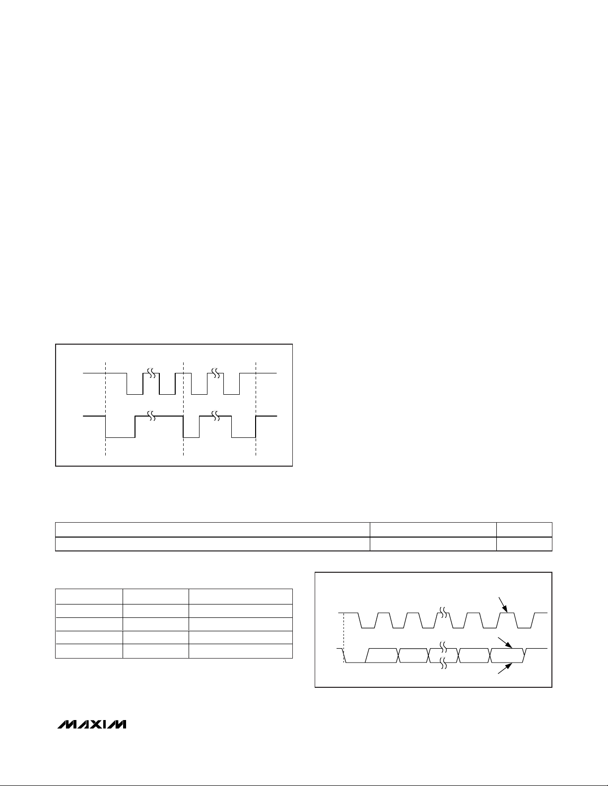
External Clock Mode
The SYNC input allows the MAX9744 to be synchronized to an external clock or another Maxim Class D
amplifier, creating a fully synchronous system. This
minimizes clock intermodulation and allocates spectral
components of the switching harmonics to insensitive
frequency bands. Applying a clock signal between
1MHz and 1.6MHz to SYNC synchronizes the
MAX9744. The MAX9744 Class D amplifier operates at
1/4 of the SYNC frequency. For example, if SYNC is
1.6MHz, the Class D amplifier operates at 400kHz.
The external SYNC signal can be any CMOS clock
source with a 40% to 60% duty cycle. Spread-spectrum
clocks work well to reduce EMI; therefore, the
SYNCOUT signal from another MAX9744 in spreadspectrum mode is an excellent SYNC input.
SYNCOUT allows several Maxim amplifiers to be cascaded (Figure 1). The synchronized output minimizes
interference due to clock intermodulation caused by the
switching spread between single devices. Using
SYNCOUT and SYNC does not affect the audio performance of the MAX9744.
Filterless Modulation/PWM Modulation
The MAX9744 features two output modulation schemes:
filterless modulation or classic PWM. The MAX9744 output modulation schemes are selectable through
SCLK/PWM when the device is in analog mode (ADDR1
and ADDR2 = GND, Table 2) or through the I2C interface (Table 8). Maxim’s unique, filterless modulation
scheme eliminates the LC filter required by traditional
Class D amplifiers, reducing component count and conserving board space and system cost. Although the
MAX9744 meets FCC and other EMI limits with a lowcost ferrite bead filter, many applications still may want
to use a full LC-filtered output. If using a full LC filter,
audio performance is best with the MAX9744 configured
for classic PWM output.
Switching between schemes, the output is not click-andpop protected. To have click-and-pop protection when
switching between output schemes, the device must
enter shutdown mode and be configured to the new output scheme before the startup sequence is finished.
SYNCOUT
OUTL+
OUTL-
OUT+
OUT-
SYNC
MAX9744
MAX9709
OUTR+
OUTR-
SYNC
SYNC INPUT
Figure 1. Cascading Two Amplifiers’ External Clock Mode
SYNC MODE
fSW (kHz)
GND
Fixed-frequency
modulation
1200 300
Unconnected
Fixed-frequency
modulation
1440 360
V
DD
Spread-spectrum
modulation
300 ±7.5
Clocked EXT
1000 to
1600
250 to
400
Table 1. Operating Modes
f
SYNC
1200 ±30
(kHz)
MAX9744
20W Stereo Class D Speaker Amplifier
with Volume Control
______________________________________________________________________________________ 15
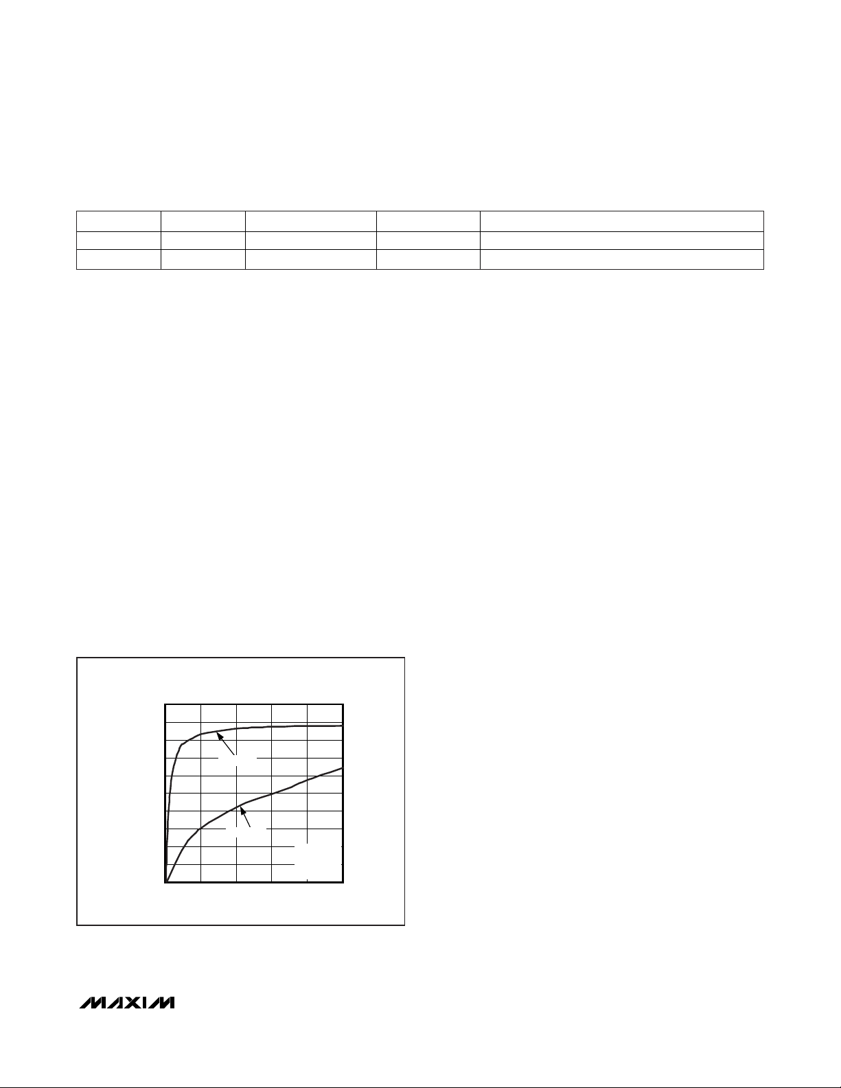
Efficiency
The high efficiency of a Class D amplifier is due to the
switching operation of the output stage transistors. In a
Class D amplifier, the output transistors act as currentsteering switches and consume negligible additional
power. Any power loss associated with the Class D output stage is mostly due to the I2R loss of the MOSFET
on-resistance, and quiescent current overhead.
The theoretical best efficiency of a linear amplifier is
78% at peak output power. Under normal operating levels (typical music reproduction levels), the efficiency
falls below 30%, whereas the MAX9744 exhibits > 80%
efficiency under the same conditions (Figure 2).
Current Limit
When the output current exceeds the current limit, 5.5A
(typ), the MAX9744 disables the outputs and initiates a
220µs startup sequence. The shutdown and startup
sequence is repeated until the output fault is removed.
Since the retry repetition is slow, the average supply
current is low. Most applications do not enter currentlimit mode unless the output is short circuited or incorrectly connected.
Thermal Shutdown
When the die temperature exceeds the thermal-shutdown threshold, +165°C (typ), the MAX9744 outputs
are disabled. Normal operation resumes when the die
temperature decreases by a factor equal to the
thermal-shutdown threshold minus the thermal-shutdown hysteresis, (typically below +150°C). The effect of
thermal shutdown is an output signal turning off for
approximately 3s in most applications, depending on
the thermal time constant of the audio system. Most
applications should never enter thermal shutdown.
Some of the possible causes of thermal shutdown are
too low of a load impedance, bad thermal contact
between the MAX9744’s exposed pad and PCB, high
ambient temperature, poor PCB layout and assembly,
or excessive output overdrive.
Shutdown
The MAX9744 features a shutdown mode that reduces
power consumption and extends battery life. Driving
SHDN low places the device in low-power shutdown
mode. Connect SHDN to digital high for normal operation. In shutdown mode, the outputs are high impedance, SYNCOUT is pulled high, BIAS voltage decays to
zero, and the common-mode input voltage decays to
zero. The I
2
C register does not retain its contents dur-
ing shutdown (MAX9744).
Mute Function
The MAX9744 features a clickless-and-popless mute
mode. When the device is muted, the outputs do not
stop switching; only the volume level is muted to the
speaker. Mute only affects the output stage and does
not shut down the device. To mute the MAX9744, drive
MUTE to logic-high. MUTE should be held high during
system power-up and power-down to ensure that pops
caused by circuits before the MAX9744 are eliminated.
To reduce clicks and pops, the device enters or exits
mute at zero crossing.
Figure 2. MAX9744 Efficiency vs. Class AB Efficiency
Table 2. Modulation Scheme Selection
ADDR2 ADDR1 SDA/VOL SCLK/PWM FUNCTION
0 0 Analog volume control 0 Filterless modulation
0 0 Analog volume control 1 Classic PWM (50% duty cycle)
EFFICIENCY
vs. OUTPUT POWER
100
90
80
70
60
50
40
EFFICIENCY (%)
30
20
10
0
010
MAX9744
CLASS AB
OUTPUT POWER (W)
PVDD = 12V
= 1kHz
f
IN
= 4Ω
R
L
8642
MAX9744/45 fig02

MAX9744
20W Stereo Class D Speaker Amplifier
with Volume Control
16 ______________________________________________________________________________________
Volume Control
For maximum flexibility, the MAX9744 features volume
control operation using an analog voltage input or
through the I2C interface. To set the device to analog
mode, connect ADDR1 and ADDR2 to GND. In analog
mode, SDA/VOL is an analog input for volume control.
The analog input range is ratiometric between 0.9 x
VDDand 0.1 x VDDwhere 0.9 x VDD= full mute and 0.1
x VDD= full volume (Table 7).
Use ADDR1 and ADDR2 to select I2C mode. There are
three addresses that can be chosen, allowing for multiple devices on a single bus (Table 4). In I2C mode, volume is controlled by choosing the speaker volume
control register in the command byte (Table 5). There
are 64 volume settings, where the lowest setting is full
mute (Table 6). See the
Write Byte
section for more
information on formatting data and tables to set volume
levels. The default volume after power-up is position 40
(-7.1dB) (see Table 7).
I2C Interface
The MAX9744 features an I2C 2-wire serial interface
consisting of a serial-data line (SDA) and a serial-clock
line (SCL). SDA and SCL facilitate communication
between the MAX9744 and the master at clock rates up
to 400kHz. Figure 3 shows the 2-wire interface timing
diagram. The MAX9744 is a receive-only slave device,
relying on the master to generate the SCL signal. The
MAX9744 cannot write to the SDA bus except to
acknowledge the receipt of data from the master. The
master, typically a microcontroller, generates SCL and
initiates data transfer on the bus.
A master device communicates to the MAX9744 by
transmitting the proper address followed by the data
word. Each transmit sequence is framed by a START (S)
or Repeated START (Sr) condition and a STOP (P) condition. Each word transmitted over the bus is 8 bits long
and is always followed by an acknowledge clock pulse.
The MAX9744 SDA line operates as both an input and
an open-drain output. A pullup resistor, greater than
500Ω, is required on the SDA bus. The MAX9744 SCL
line operates as an input only. A pullup resistor, greater
than 500Ω, is required on SCL if there are multiple masters on the bus, or if the master in a single-master system has an open-drain SCL output. Series resistors in
line with SDA and SCL are optional. The SCL and SDA
inputs have Schmitt trigger and filter circuits that suppress noise spikes to assure proper device operation
even on a noisy bus.
Figure 3. 2-Wire Serial-Interface Timing Diagram
SDA
t
SU, DAT
t
LOW
SCL
t
t
HD, STA
START
CONDITION
HIGH
t
R
t
HD, DAT
t
F
t
SU, STA
REPEATED
START
CONDITION
t
HD, STA
t
SP
t
SU, STO
STOP
CONDITION
t
BUF
START
CONDITION
MAX9744
20W Stereo Class D Speaker Amplifier
with Volume Control
______________________________________________________________________________________ 17
Bit Transfer
One data bit is transferred during each SCL cycle. The
data on SDA must remain stable during the high period
of the SCL pulse. Changes in SDA while SCL is high
are control signals (see the
START and STOP
Conditions
section). SDA and SCL idle high when the
I
2
C bus is not busy.
START and STOP Conditions
A master device initiates communication by issuing a
START condition. A START condition is a high to low
transition on SDA with SCL high. A STOP condition is a
low to high transition on SDA while SCL is high (Figure
4). A START (S) condition from the master signals the
beginning of a transmission to the MAX9744. The master terminates transmission, and frees the bus, by issuing a STOP (P) condition. The bus remains active if a
Repeated START (Sr) condition is generated instead of
a STOP condition.
Early STOP Conditions
The MAX9744 recognizes a STOP condition at any point
during data transmission except if the STOP condition
occurs in the same high pulse as a START condition.
Slave Address
The slave address of the MAX9744 is 8 bits and consists of 3 fields: the first field is 5 bits wide and is fixed
(10010), the second is a 2 bit field which is set through
ADDR1 and ADDR2 (externally connected as logic-high
or logic-low), and the third field is a R/W flag bit. Set
R/W = 0 to write to the slave. A representation of the
slave address is shown in Table 3.
When ADDR1 and ADDR2 are connected to GND, serial interface communication is disabled. Table 4 summarizes the slave address of the device as a function of
ADDR1 and ADDR2.
Acknowledge
The acknowledge bit (ACK) is a clocked 9th bit that the
MAX9744 uses to handshake receipt of each byte of
data (see Figure 5). The MAX9744 pulls down SDA during the master-generated 9th clock pulse. The SDA line
must remain stable and low during the high period of
the acknowledge clock pulse. Monitoring ACK allows
for detection of unsuccessful data transfers. An unsuccessful data transfer occurs if a receiving device is
busy or if a system fault has occurred. In the event of
an unsuccessful data transfer, the bus master may reattempt communication.
Figure 4. START, STOP, and Repeated START Conditions
Figure 5. Acknowledge
Table 3. Slave Address Block
Table 4. Slave Address
SSrP
SCL
SDA
SA7 (MSB) SA6 SA5 SA4 SA3 SA2 SA1 SA0 (LSB)
1 0 0 1 0 ADDR2 ADDR1 R/W
ADDR2 ADDR1 SLAVE ADDRESS
00I
0 1 1001001_
1 0 1001010_
1 1 1001011_
2
C disabled
START
CONDITION
SCL
SDA
1
29
CLOCK PULSE FOR
ACKNOWLEDGMENT
8
NOT ACKNOWLEDGE
ACKNOWLEDGE
MAX9744
Write Byte
A write to the MAX9744 includes transmission of a
START condition, the slave address with the R/W bit set
to 0 (see Table 3), one byte of data to the command
register, and a STOP condition. Figure 6 illustrates the
proper format for one frame.
A write to the MAX9744 consists of a 6-step sequence
as seen below:
1) The master sends a START condition.
2) The master sends the 7 bits slave ID plus a write
bit (low).
3) The addressed slave asserts an ACK on the data
line.
4) The master sends 8 data bits.
5) The active slave asserts an ACK (or NACK) on the
data line.
6) The master generates a stop condition.
Speaker Volume Control
The command register is used to control the volume
level of the speaker amplifier. The two MSBs (A1 and
A0) are set to 00, while V5–V0 is the data that is written
into the addresses register to set the volume level
(Tables 5 and 6).
Filterless Modulation/PWM
The MAX9744 features two output modulation schemes:
filterless modulation or classic PWM, selectable through
the I2C interface. Table 6 shows the register command
to set the output scheme.
When switching between schemes, the output is not
click-and-pop protected. To have click-and-pop protection when switching between output schemes, the
device must enter shutdown mode and be configured
to the new output scheme before the 220ms startup
sequence is terminated.
20W Stereo Class D Speaker Amplifier
with Volume Control
18 ______________________________________________________________________________________
Figure 6. Write Byte Format Example
Table 5. Data Byte Format
Table 6. Command Register Programming
WRITE BYTE FORMAT
S SLAVE ADDRESS
7 BITS
EQUIVALENT TO CHIPSELECT LINE OF A
3-WIRE INTERFACE.
WR ACK DATA
0
8 BITS
DATA BYTE: GIVES A COMMAND.SLAVE ADDRESS:
ACK P
D7 (MSB) D6 D5 D4 D3 D2 D1 D0 (LSB)
A1 A0 V5 V4 V3 V2 V1 V0
A0A
1
00 XXXXXX Volume level (Table 7)
01 000000 Filterless modulation
01 000001 Classic PWM
V5–V0 SETTING
A0A
1
10 XXXXXX Reserved
11 000100 Increased volume
11 000101 Decreased volume
V5–V0 SETTING

MAX9744
20W Stereo Class D Speaker Amplifier
with Volume Control
______________________________________________________________________________________ 19
Table 7. Speaker Volume Levels
V5 V4 V3 V2 V1 V0
1 1 1 1 1 1 63 0.100 x V
1 1 1 1 1 0 62 0.113 x V
1 1 1 1 0 1 61 0.125 x V
1 1 1 1 0 0 60 0.138 x V
1 1 1 0 1 1 59 0.151 x V
1 1 1 0 1 0 58 0.163 x V
1 1 1 0 0 1 57 0.176 x V
1 1 1 0 0 0 56 0.189 x V
1 1 0 1 1 1 55 0.202 x V
1 1 0 1 1 0 54 0.214 x V
1 1 0 1 0 1 53 0.227 x V
1 1 0 1 0 0 52 0.240 x V
1 1 0 0 1 1 51 0.252 x V
1 1 0 0 1 0 50 0.265 x V
1 1 0 0 0 1 49 0.278 x V
1 1 0 0 0 0 48 0.290 x V
1 0 1 1 1 1 47 0.303 x V
1 0 1 1 1 0 46 0.316 x V
1 0 1 1 0 1 45 0.329 x V
1 0 1 1 0 0 44 0.341 x V
1 0 1 0 1 1 43 0.354 x V
1 0 1 0 1 0 42 0.367 x V
1 0 1 0 0 1 41 0.379 x V
1 0 1 0 0 0 40 0.392 x V
1 0 0 1 1 1 39 0.405 x V
1 0 0 1 1 0 38 0.417 x V
1 0 0 1 0 1 37 0.430 x V
1 0 0 1 0 0 36 0.443 x V
1 0 0 0 1 1 35 0.456 x V
1 0 0 0 1 0 34 0.468 x V
1 0 0 0 0 1 33 0.481 x V
1 0 0 0 0 0 32 0.494 x V
VOLUME
POSITION
VOLUME INPUT VOLTAGE (V) ATTENUATION (dB)
SDA/VOL VOLUME
DD
DD
DD
DD
DD
DD
DD
DD
DD
DD
DD
DD
DD
DD
DD
DD
DD
DD
DD
DD
DD
DD
DD
DD
DD
DD
DD
DD
DD
DD
DD
DD
9.5
8.8
8.2
7.6
7.0
6.5
5.9
5.4
4.9
4.4
3.9
3.4
2.9
2.4
2.0
1.6
1.2
0.5
-0.5
-1.9
-3.4
-5.0
-6.0
-7.1
-8.9
-9.9
-10.9
-12.0
-13.1
-14.4
-15.4
-16.4

MAX9744
20W Stereo Class D Speaker Amplifier
with Volume Control
20 ______________________________________________________________________________________
Table 7. Speaker Volume Levels (continued)
V5 V4 V3 V2 V1 V0
0 1 1 1 1 1 31 0.506 x V
0 1 1 1 1 0 30 0.519 x V
0 1 1 1 0 1 29 0.532 x V
0 1 1 1 0 0 28 0.544 x V
0 1 1 0 1 1 27 0.557 x V
0 1 1 0 1 0 26 0.570 x V
0 1 1 0 0 1 25 0.583 x V
0 1 1 0 0 0 24 0.595 x V
0 1 0 1 1 1 23 0.608 x V
0 1 0 1 1 0 22 0.621 x V
0 1 0 1 0 1 21 0.633 x V
0 1 0 1 0 0 20 0.646 x V
0 1 0 0 1 1 19 0.659 x V
0 1 0 0 1 0 18 0.671 x V
0 1 0 0 0 1 17 0.684 x V
0 1 0 0 0 0 16 0.697 x V
0 0 1 1 1 1 15 0.710 x V
0 0 1 1 1 0 14 0.722 x V
0 0 1 1 0 1 13 0.735 x V
0 0 1 1 0 0 12 0.748 x V
0 0 1 0 1 1 11 0.760 x V
0 0 1 0 1 0 10 0.773 x V
0 0 1 0 0 1 9 0.786 x V
0 0 1 0 0 0 8 0.798 x V
0 0 0 1 1` 1 7 0.811 x V
0 0 0 1 1 0 6 0.824 x V
0 0 0 1 0 1 5 0.837 x V
0 0 0 1 0 0 4 0.849 x V
0 0 0 0 1 1 3 0.862 x V
0 0 0 0 1 0 2 0.875 x V
0 0 0 0 0 1 1 0.887 x V
0 0 0 0 0 0 0 0.900 x V
VOLUME
POSITION
SDA/VOL VOLUME
VOLUME INPUT VOLTAGE (V) ATTENUATION (dB)
DD
DD
DD
DD
DD
DD
DD
DD
DD
DD
DD
DD
DD
DD
DD
DD
DD
DD
DD
DD
DD
DD
DD
DD
DD
DD
DD
DD
DD
DD
DD
DD
-17.5
-19.7
-21.6
-23.5
-25.2
-27.2
-29.8
-31.5
-33.4
-36.0
-37.6
-39.6
-42.1
-43.7
-45.6
-48.1
-50.6
-54.2
-56.7
-60.2
-62.7
-66.2
-68.7
-72.2
-74.7
-78.3
-80.8
-84.3
-86.8
-90.3
-92.8
MUTE

MAX9744
Applications Information
Filterless Class D Operation
The MAX9744 meets common EMC radiation limits without a filter when the speaker leads are less than approximately 10cm. Using lengths beyond 10cm is possible
verifying against the appropriate EMC standard.
For longer speaker wire lengths, up to approximately
1m, use a simple ferrite bead and capacitor filter to
meet EMC limits. Select a ferrite bead with 100Ω to
600Ω impedance, and rated for at least 3A. The capacitor value varies based on the ferrite bead chosen and
the actual speaker lead length. Select the capacitor
value based on EMC performance. See Figure 7 for the
correct connections of these components.
When evaluating the device without a filter or a ferrite
bead filter, include a series inductor (68µH for 8Ω load
and 33µH for 4Ω load) to model the actual loudspeaker’s behavior. Omitting this inductor reduces the efficiency, the THD+N performance, and the output power
of the MAX9744.
Inductor-Based Output Filters
Some applications use the MAX9744 with a full inductor/capacitor-based (LC) output filter. This is common
for longer speaker lead lengths and to gain increased
margin to EMC limits. Select the PWM output mode and
use fixed-frequency modulation mode for best audio
performance. See Figure 8 for the correct connections
of these components.
The component selection is based on the load impedance of the speaker. Table 8 lists suggested values for
a variety of load impedances.
Inductors L1 and L2 and capacitor C1 form the primary
output filter. In addition to these primary filter components, other components in the filter improve its functionality. Capacitors C4 and C5 plus resistors R1 and
R2 form a Zobel at the output. A Zobel corrects the output loading to compensate for the rising impedance of
the loudspeaker. Without a Zobel, the filter has a peak
in its response near the cutoff frequency. Capacitors
C2 and C3 provide common-mode noise suppression
to reduce radiated emissions.
20W Stereo Class D Speaker Amplifier
with Volume Control
______________________________________________________________________________________ 21
Table 8. Suggested Values for LC filter
Figure 7. Ferrite Bead Filter
Figure 8. Output Filter for PWM Mode
BOOT_+
C
BOOT
MAX9744
OUT_+
OUT_-
BOOT_-
0.1μF
C
BOOT
0.1μF
C
FILT
470pF
C
FILT
470pF
RL (Ω)
L1, L2
(µH)
4 10 0.47 0.47 10 0.47
6 15 0.33 0.22 15 0.33
8 22 0.22 0.22 22 0.22
C1 (µF)
C2, C3
(µF)
R1, R2
(Ω)
C4, C5
(µF)
MAX9744
1, 2
14, 18
BOOT+
4
OUT+
OUT-
BOOT-
15
C
BOOT
0.1μF
C
BOOT
0.1μF
L1
C2
L2
C3
C4
C1
C5
R1
R2
R
L

Figure 9. Setting Gain
Figure 10. Using a Linear Regulator to Produce 3.3V from a
Higher Power Supply
MAX9744
20W Stereo Class D Speaker Amplifier
with Volume Control
22 ______________________________________________________________________________________
Component Selection
Gain-Setting Resistors
External feedback resistors set the gain of the
MAX9744. The output stage has an internal 20dB gain
in addition to the externally set input stage gain. Set the
maximum gain by using resistors RFand RIN(Figure 9)
as follows:
Choose RFbetween 10kΩ and 50kΩ. Note that the
actual gain of the amplifier is dependent on the volume
level setting. For example, with the volume set to
+9.5dB, the amplifier gain would be 9.5dB plus 20dB,
assuming RIN= RF.
The input amplifier can be configured into a variety of
circuits. The FB terminal is an actual operational amplifier output, allowing the MAX9744 to be configured as a
summing amplifier, a filter, or an equalizer, for example.
Input Capacitor
An input capacitor (CIN) in conjunction with the input
impedance of the MAX9744 form a highpass filter that
removes the DC bias from an incoming signal. The ACcoupling capacitor allows the amplifier to automatically
bias the signal to an optimum DC level. Assuming zero
source impedance, the -3dB point of the highpass filter
is given by:
Choose CINthat f
-3dB
is well below the lowest frequency of interest. Use capacitors whose dielectrics have
low-voltage coefficients, such as tantalum or aluminum
electrolytic. Capacitors with high-voltage coefficients,
such as ceramics, may result in increased distortion at
low frequencies.
DC-Coupled Input
The input amplifier can accept DC-coupled inputs that
are biased to the amplifier’s bias voltage. DC-coupling
eliminates input-coupling capacitors, reducing component count to potentially one external component. In this
configuration the highpass filtering effect of the capacitors
is lost, allowing low-frequency signals to be amplified.
Power Supplies
The MAX9744 features separate supplies for each portion of the device, allowing for the optimum combination
of headroom power dissipation and noise immunity. The
speaker amplifier is powered from PVDD and can range
from 4.5V to 14V. The remainder of the device is powered by VDD. Power supplies are independent of each
other so sequencing is not necessary. Power may be
supplied by separate sources or derived from a single
higher source using a linear regulator (Figure 10).
BIAS Capacitor
BIAS is the output of the internally generated DC bias
voltage. The BIAS bypass capacitor, C
BIAS
, improves
PSRR and THD+N by reducing power supply and other
noise sources at the common-mode bias node, and
also generates the clickless/popless, startup/shutdown,
DC bias waveforms for the speaker amplifiers. Bypass
BIAS with a 2.2µF capacitor to GND.
f
RC
dB
IN IN
−
=
3
1
2π
A
R
R
VV
V
F
IN
=
⎛
⎝
⎜
⎞
⎠
⎟
−30 /
4.5V TO 14.5V
MAX9744
AUDIO
C
IN
R
INPUT
IN
IN
VOLUME
R
CONTROL
F
FB
9.5dB (max)
20dB
CLASS D
BOOT+
OUT+
OUT-
BOOT-
PV
MAX9744
GND
DD
MAX1615
IN
GND
OUT
3.3V
V
DD
1μF
SHDN
1μF

MAX9744
Supply Bypassing, Layout,
and Grounding
Proper layout and grounding are essential for optimum
performance. Use large traces for the power-supply
inputs and amplifier outputs to minimize losses due to
parasitic trace resistance. Large traces also aid in moving heat away from the package. Proper grounding
improves audio performance, minimizes crosstalk
between channels, and prevents any switching noise
from coupling into the audio signal. Connect PGND and
GND together at a single point on the PCB. Route all
traces that carry switching transients away from GND
and the traces/components in the audio signal path.
Connect all PVDD power supplies together and bypass
with a 1µF capacitor to PGND. Connect all V
DD
power
supplies together and bypass with a 1µF capacitor to
GND. Place a bulk capacitor between PVDD and PGND
if needed.
Use large, low-resistance output traces. Current drawn
from the outputs increase as load impedance decreases. High output trace resistance decreases the power
delivered to the load. Large output, supply, and GND
traces allow more heat to move from the MAX9744 to
the air, decreasing the thermal impedance of the circuit.
The MAX9744 thin QFN package features an exposed
thermal pad on its underside. This pad lowers the package’s thermal resistance by providing a direct heat conduction path from the die to the PCB. Connect the
exposed thermal pad to PGND by using a large pad and
multiple vias to the PGND plane. The exposed pad must
be connected to PGND for proper device operation.
20W Stereo Class D Speaker Amplifier
with Volume Control
______________________________________________________________________________________ 23
Pin Configuration
TOP VIEW
PGND
PGND
OUTR-
OUTR-
BOOTR-
PGND
BOOTL-
OUTL-
OUTL-
PGND
PGND
OUTR+
PVDD
OUTR+
BOOTR+
32
31 30 29 28 27 26 25 24
33
34
35
36
37
38
39
40
41
42
43
+
44
2
1
OUTL+
BOOTL+
MAX9744
345
PVDD
PVDD
OUTL+
678910
SYNCOUT
GND
VDDPVDD
DD
V
GND
SDA/VOL
MUTE
SYNC
23
11
DD
V
SCLK/PWM
N.C.
GND
SHDN
22
V
21
DD
20
BIAS
19
INR
FBR
18
FBL
17
16
INL
15
GND
14
ADDR2
ADDR1
13
GND
12
TQFN
(7mm x 7mm)

Functional Diagrams/Typical Application Circuits
MAX9744
20W Stereo Class D Speaker Amplifier
with Volume Control
24 ______________________________________________________________________________________
I2C MODE
C
R
IN
0.47μF
0.47μF
20kΩ
C
R
IN
20kΩ
V
DD
3V TO 3.6V
1μF
R
F
IN
IN
20kΩ
R
20kΩ
TO μC
V
DD
F
FBL 17
INL 16
INR 19
FBR 18
MUTE 24
SHDN
SDA/VOL
SCLK 9
ADDR1 13
ADDR2 14
SYNC
22
8
25
6, 10, 21, 28
MAX9744
BIAS
MUTE
SHUTDOWN
CONTROL
2
I
ANALOG
CONTROL
V
DD
VOLUME
CONTROL
C
OSCILLATOR
4.5V TO 14V
PVDD
4, 5, 29, 30
CLASS DCLASS D
PV
DD
36, 37
C
BOOT
0.1μF
C
BOOT
0.1μF
C
BOOT
0.1μF
C
BOOT
0.1μF
SYNCOUT
100μF
1μF
BOOTL+1
OUTL+2, 3
OUTL-41, 42
BOOTL-40
BOOTR+33
OUTR+31, 32
OUTR-
BOOTR-38
26
BIAS
20
(SHOWN IN I
2
C MODE, AV = 29.5dB, f
N.C.
23
7, 11, 12,
15, 27
= 17Hz, SPREAD-SPECTRUM MODE, MUTE OFF, SLAVE ADDRESS = 1001011_)
-3dB
34, 35, 39, 43, 44
BIAS
PGNDGND
C
BIAS
2.2μF

MAX9744
20W Stereo Class D Speaker Amplifier
with Volume Control
______________________________________________________________________________________ 25
Functional Diagrams/Typical Application Circuits (continued)
C
IN
0.47μF
C
IN
0.47μF
ANALOG MODE
3V TO 3.6V 4.5V TO 14V
C
BOOT
0.1μF
C
BOOT
0.1μF
C
BOOT
0.1μF
C
BOOT
0.1μF
SYNCOUT
100μF
1μF
R
F
R
IN
20kΩ
R
IN
20kΩ
V
DD
20kΩ
R
20kΩ
V
DD
F
MUTE 24
SHDN
SDA/VOL 8
SCLK/PWM 9
ADDR1 13
ADDR2 14
SYNC
FBL 17
INL 16
INR 19
FBR 18
MAX9744
22
25
V
6, 10, 21, 28
BIAS
MUTE
SHUTDOWN
CONTROL
2
C
I
OUTPUT
MODULATION
ANALOG
CONTROL
DD
VOLUME
CONTROL
OSCILLATOR
PV
DD
PVDD
4, 5, 29, 30
CLASS DCLASS D
36, 37
26
1μF
BOOTL+1
OUTL+2, 3
OUTL-41, 42
BOOTL-40
BOOTR+33
OUTR+31, 32
OUTR-
BOOTR-38
(SHOWN IN ANALOG MODE, AV = 29.5dB, f
N.C.
23
7, 11, 12,
15, 27
= 17Hz, SPREAD-SPECTRUM MODE, MUTE OFF, SLAVE ADDRESS = 1001011_)
-3dB
34, 35, 39, 43, 44
BIAS
BIAS
20
C
BIAS
2.2μF
PGNDGND
MAX9744
20W Stereo Class D Speaker Amplifier
with Volume Control
26 ______________________________________________________________________________________
Package Information
For the latest package outline information and land patterns, go to www.maxim-ic.com/packages.
E
E/2
D/2
D
A1AA2
DETAIL A
(ND-1) X e
(NE-1) X e
e
L
k
C
L
L
E2/2
C
L
E2
e
PACKAGE OUTLINE,
32, 44, 48, 56L THIN QFN, 7x7x0.8mm
k
C
D2
L
D2/2
b
C
L
e
21-0144 G
32, 44, 48L QFN.EPS
L
1
2
MAX9744
20W Stereo Class D Speaker Amplifier
with Volume Control
______________________________________________________________________________________ 27
Chip Information
PROCESS: BICMOS
PACKAGE TYPE PACKAGE CODE DOCUMENT NO.
44 TQFN-EP T4477-3
21-0144
Package Information (continued)
For the latest package outline information and land patterns, go to www.maxim-ic.com/packages.
PACKAGE OUTLINE,
32, 44, 48, 56L THIN QFN, 7x7x0.8mm
21-0144 G
2
2

Revision History
MAX9744
20W Stereo Class D Speaker Amplifier
with Volume Control
Maxim cannot assume responsibility for use of any circuitry other than circuitry entirely embodied in a Maxim product. No circuit patent licenses are
implied. Maxim reserves the right to change the circuitry and specifications without notice at any time.
28
____________________Maxim Integrated Products, 120 San Gabriel Drive, Sunnyvale, CA 94086 408-737-7600
© 2008 Maxim Integrated Products is a registered trademark of Maxim Integrated Products, Inc.
REVISION
NUMBER
0 3/08 Initial release —
1 9/08 Updated EC table for single pass flow 2, 4, 5
REVISION
DATE
DESCRIPTION
PAGES
CHANGED
 Loading...