


General Description
The MAX9742 stereo Class D audio power amplifier
delivers up to 2 x 16W into 4Ω loads. The MAX9742
features high-power efficiency (92% with 8Ω loads),
eliminating the need for a bulky heatsink and conserving power. The MAX9742 operates from a 20V to 40V
single supply or a ±10V to ±20V dual supply. Features
include fully differential inputs, comprehensive clickand-pop suppression, low-power shutdown mode, and
an externally adjustable gain. Short-circuit and thermaloverload protection prevent the device from being
damaged during a fault condition.
The MAX9742 is available in a thermally efficient 36-pin
TQFN (6mm x 6mm x 0.8mm) package and is specified
over the -40°C to +85°C extended temperature range.
Applications
CRT TVs
Flat-Panel Display TVs
Audio Docking Stations
Multimedia Monitors
Features
2 x 16W Output Power (RL= 4Ω, THD+N = 10%)
High Efficiency: Up to 92% with RL= 8Ω
Mute and Shutdown Modes
Differential Inputs Suppress Common-Mode Noise
Adjustable Gain
Integrated Click-and-Pop Suppression
Low 0.06% THD+N at 3.5W, RL= 8Ω
Output Short-Circuit and Thermal Protection
Available in Space-Saving, 6mm x 6mm, 36-Pin
TQFN Package
MAX9742
Single-/Dual-Supply, Stereo 16W,
Class D Amplifier with Differential Inputs
________________________________________________________________
Maxim Integrated Products
1
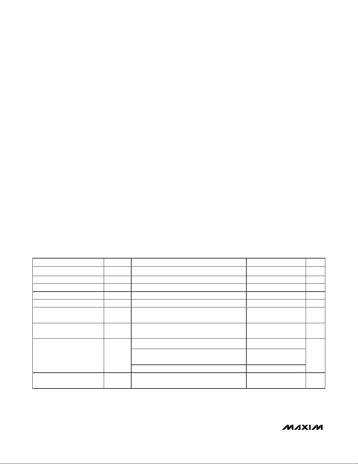
Simplified Block Diagrams
19-0731; Rev 0; 1/07
For pricing, delivery, and ordering information, please contact Maxim/Dallas Direct! at
1-888-629-4642, or visit Maxim’s website at www.maxim-ic.com.
EVALUATION KIT
AVAILABLE
Pin Configuration located at end of data sheet.
Ordering Information
+
Denotes lead-free package.
*
EP = Exposed paddle.
Simplified Block Diagrams continued at end of data sheet.
SINGLE-SUPPLY CONFIGURATION
C
FBL
PART TEMP RANGE PIN-PACKAGE
MAX9742ETX+ -40°C to +85°C 36 TQFN-EP* T3666-3
PKG
CODE
R
F1
20V TO 40V
FBL
V
DD
MAX9742
CLASS D
MODULATOR AND
HALF-BRIDGE
CLASS D
MODULATOR AND
HALF-BRIDGE
CONTROL LOGIC/
POWER-UP
SEQUENCING
FBR SFT
V
SHDN
SS
ON
OFF
R
F1
C
L
OUTL
OUTR
C
SFT
F
L
F
OUT
R
C
C
ZBL
F
C
ZBL
C
OUT
R
ZBL
F
C
ZBL
LEFT NEGATIVE
AUDIO INPUT
LEFT POSITIVE
AUDIO INPUT
RIGHT POSITIVE
AUDIO INPUT
RIGHT NEGATIVE
AUDIO INPUT
C
IN
R
IN1
C
IN
R
IN2
C
R
F2
V
DD
2
R
C
F2
C
IN
R
IN2
C
IN
R
IN1
INL-
INL+
FBL
MID
FBR
INR+
INR-
C
FBR
MAX9742
Single-/Dual-Supply, Stereo 16W,
Class D Amplifier with Differential Inputs
2 _______________________________________________________________________________________
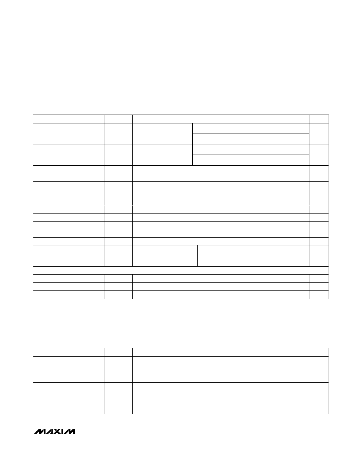
ABSOLUTE MAXIMUM RATINGS
ELECTRICAL CHARACTERISTICS—Single-Supply, Single-Ended Output
(VDD= 24V, VSS= V
SUB
= LGND = 0V, V
SHDN
= 3.3V, V
MID
= 12V, C
VDD
= 660µF, C
MID1
= 10µF, C
MID2
= 10µF, R1 = R2 = R3 =
10kΩ, C
SFT
= 0.47µF, C
OUT
= 1000µF, C
FB_1
= 150pF, C
FB_2
= 10pF, C
BOOT
= 0.1µF, C
REGP
= C
REGM
= 1µF, R
IN_
= 30.1kΩ,
R
F1A
= 121kΩ, R
F1B
= 562kΩ, RF2= 681kΩ, R
REF
= 68kΩ, RL= ∞, TA= T
MIN
to T
MAX
, unless otherwise noted. Typical values are at
T
A
= +25°C.) (Note 2)
Stresses beyond those listed under “Absolute Maximum Ratings” may cause permanent damage to the device. These are stress ratings only, and functional
operation of the device at these or any other conditions beyond those indicated in the operational sections of the specifications is not implied. Exposure to
absolute maximum rating conditions for extended periods may affect device reliability.
VDDto VSS, NSENSE ..............................................-0.3V to +45V
MID, LGND, LV
DD
, REGM, REGP, OUTR,
OUTL to V
SS
.......................................................-0.3V to +45V
MID, LGND, LV
DD
, REGM, REGP, OUTR,
OUTL to V
DD
.......................................................-45V to +0.3V
REGLS to V
SS
.........................................................-0.3V to +12V
MID to REGP, REGM...............(V
REGM
- 0.3V) to (V
REGP
+ 0.3V)
REGP to REGM.......................................................-0.3V to +12V
LV
DD
to LGND..........................................................-0.3V to +6V
SHDN to LGND.........................................................-0.3V to +4V
SFT to LGND ............................................................-0.3V to +6V
FB_, IN_+, IN_-, REFCUR to REGP,
REGM..................................(V
REGM
- 0.3V) to (V
REGP
+ 0.3V)
BOOTR to OUTR ....................................................-0.3V to +12V
BOOTL to OUTL .....................................................-0.3V to +12V
OUTR, OUTL Shorted to LGND..................................Continuous
Continuous Power Dissipation (T
A
= +70°C) (Note 1)
Single-Layer Board:
36-Pin TQFN (derate 26.3mW/°C above +70°C) ...........2.11W
Multilayer Board:
36-Pin TQFN (derate 35.7mW/°C above +70°C) ...........2.86W
Junction-to-Ambient Thermal Resistance (θ
JA
)
Single-Layer Board:
36-Pin TQFN.................................................................38°C/W
Multilayer Board:
36-Pin TQFN.................................................................28°C/W
Junction-to-Case Thermal Resistance (θ
JC
) ...................1.4°C/W
Operating Temperature Range ...........................-40°C to +85°C
Maximum Junction Temperature .....................................+150°C
Storage Temperature Range .............................-65°C to +150°C
Lead Temperature (soldering, 10s) .................................+300°C
Note 1: Actual power capabilities are dependent on PCB layout. See the
Thermal Considerations
section.
PARAMETER SYMBOL CONDITIONS MIN TYP MAX UNITS
Supply Voltage Range V
Supply Current I
Mute Mode Supply Current No load, V
Shutdown Current No load, V
Switching Frequency f
Power-Supply Rejection Ratio
(Note 4)
Crosstalk
(Notes 5 and 6)
Continuous Output Power
(Notes 5, 6, and 7)
Efficiency
(Notes 5, 6, and 7)
DD
DD
SW
PSRR V
P
OUT
(Note 3) 20 40 V
No load, output filter removed 15 mA
= 0V (outputs not switching) 8 mA
SFT
= 0V 0.8 1.3 mA
SHDN
= 24V + 500mV
DD
L to R, R to L, R
, f = 1kHz 68 dB
P-P
= 8Ω, P
L
= 1W, f = 1kHz -78 dB
OUT
RL = 8Ω, fIN = 1kHz, THD+N = 10% 9.5
RL = 8Ω, fIN = 1kHz, THD+N = 10%,
= 35V
V
DD
RL = 4Ω, fIN = 1kHz, THD+N = 10% 16
R
= 8Ω, P
L
= 9.5W, THD+N = 10% 92 %
OUT
300 kHz
20.5
W
MAX9742
Single-/Dual-Supply, Stereo 16W,
Class D Amplifier with Differential Inputs
_______________________________________________________________________________________ 3
)
ELECTRICAL CHARACTERISTICS—Single-Supply, Single-Ended Output (continued)
(VDD= 24V, VSS= V
SUB
= LGND = 0V, V
SHDN
= 3.3V, V
MID
= 12V, C
VDD
= 660µF, C
MID1
= 10µF, C
MID2
= 10µF, R1 = R2 = R3 =
10kΩ, C
SFT
= 0.47µF, C
OUT
= 1000µF, C
FB_1
= 150pF, C
FB_2
= 10pF, C
BOOT
= 0.1µF, C
REGP
= C
REGM
= 1µF, R
IN_
= 30.1kΩ,
R
F1A
= 121kΩ, R
F1B
= 562kΩ, RF2= 681kΩ, R
REF
= 68kΩ, RL= ∞, TA= T
MIN
to T
MAX
, unless otherwise noted. Typical values are at
T
A
= +25°C.) (Note 2)
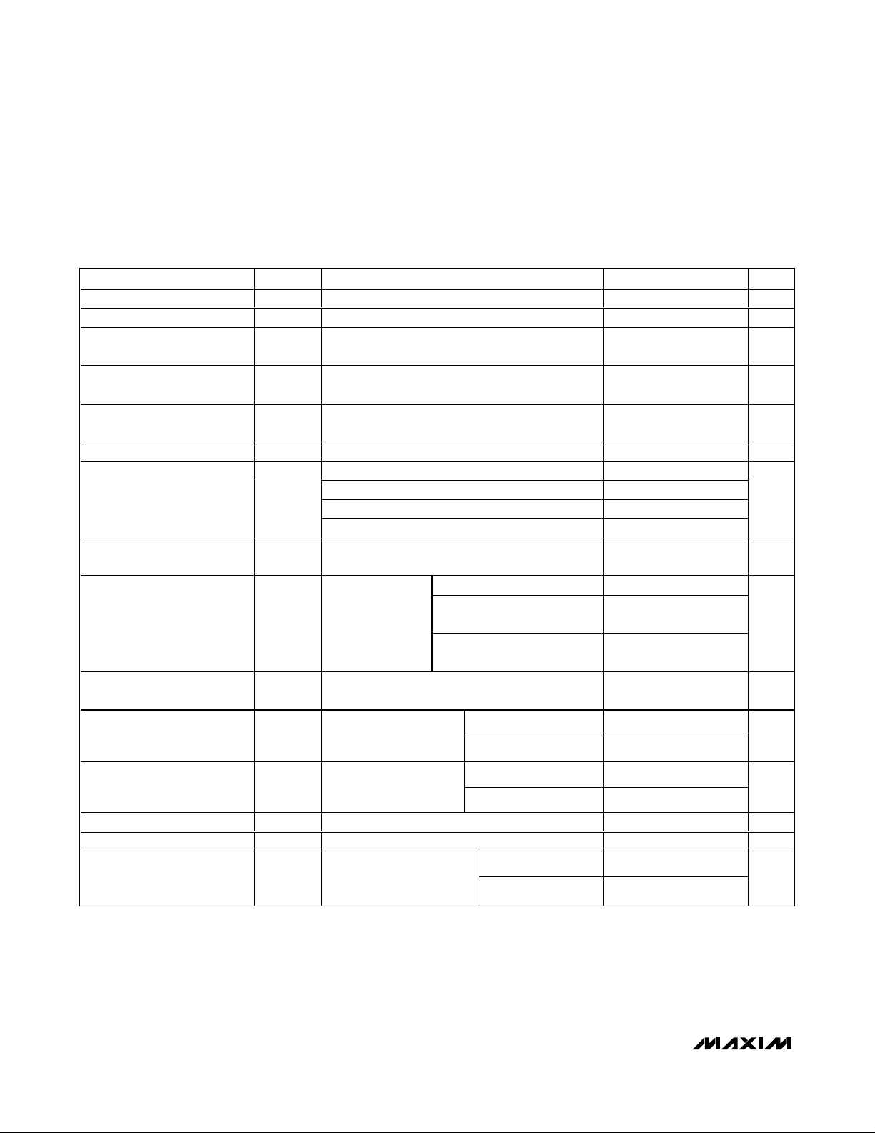
ELECTRICAL CHARACTERISTICS—Dual Supplies
(VDD= 15V, VSS= V
SUB
= -15V, V
SHDN
= 3.3V, V
MID
= LGND = 0V, C
VDD
= C
VSS
= 1000µF, C
BYP
= 1µF, C
SFT
= 0.22µF, C
FB_1
=
150pF, C
FB_2
= 10pF, C
BOOT
= 0.1µF, C
REGP
= C
REGM
= 1µF, R
IN_
= 30.1kΩ, R
F1A
= 121kΩ, R
F1B
= 562kΩ, RF2= 681kΩ, R
REF
=
68kΩ, R
L
= ∞, TA= T
MIN
to T
MAX
, unless otherwise noted. Typical values are at TA= +25°C.) (Note 2)
PARAMETER SYMBOL CONDITIONS MIN TYP MAX UNITS
Total Harmonic Distortion Plus
Noise
Signal-to-Noise Ratio SNR
Half-Bridge Switch
On-Resistance
Switch Rise and Fall Times No load (Note 4) 50 ns
IN_ Input Bias Current -1 +1 µA
MID Input Bias Current I
Shutdown-to-Full Operation t
Power-On to Full Operation t
Thermal-Overload Threshold
Temperature
Short-Circuit Output Current I
Click-and-Pop K
DIGITAL INPUTS (SHDN) (Note 9)
Logic-Input Low Voltage V
Logic-Input High Voltage V
Input Leakage Current -1 +1 µA
THD+N
R
DS(ON
MID
SON
PU
T
SH
SC
CP
IL
IH
f
= 1kHz,
IN
RL = 8Ω, P
= 3.5W 0.06
OUT
BW = 22Hz to 22kHz
(Notes 5, 6, and 7)
P
= 9.5W, RL = 8Ω,
OUT
= 4Ω, P
L
Unweighted 88
= 5W 0.08
OUT
R
BW = 22Hz to 22kHz
(Notes 5 and 6)
A-weighted 93
0.4 0.7 Ω
VDD = 24V, no load 50 µA
68 ms
V
= 3.3V 1.5 s
SHDN
Junction temperature 150
OUT_ shorted to VDD or V
P eak vol tag e, 32- sam p l es
SS
Into shutdown -38
2.9 4.5 A
p er second , A- w ei g hted
( N otes 4 and 8)
Out of shutdown -40
0.4 V
2.4 V
%
dB
o
C
dBV
PARAMETER SYMBOL CONDITIONS MIN TYP MAX UNITS
P osi ti ve S up p l y V ol tag e Rang eVDD(Note 3) 10 20 V
N eg ati ve S up p l y V ol tag e
Rang e
Positive Supply Mute Mode
Current
Negative Supply Mute Mode
Current
V
(Note 3) -20 -10 V
SS
No load, V
No load, V
SFT
SFT
= 0V (outputs not switching) 8 11 mA
= 0V (outputs not switching) -12 -8 mA
MAX9742
Single-/Dual-Supply, Stereo 16W,
Class D Amplifier with Differential Inputs
4 _______________________________________________________________________________________
ELECTRICAL CHARACTERISTICS—Dual Supplies (continued)
(VDD= 15V, VSS= V
SUB
= -15V, V
SHDN
= 3.3V, V
MID
= LGND = 0V, C
VDD
= C
VSS
= 1000µF, C
BYP
= 1µF, C
SFT
= 0.22µF, C
FB_1
=
150pF, C
FB_2
= 10pF, C
BOOT
= 0.1µF, C
REGP
= C
REGM
= 1µF, R
IN_
= 30.1kΩ, R
F1A
= 121kΩ, R
F1B
= 562kΩ, RF2= 681kΩ, R
REF
=
68kΩ, R
L
= ∞, TA= T
MIN
to T
MAX
, unless otherwise noted. Typical values are at TA= +25°C.) (Note 2)
PARAMETER SYMBOL CONDITIONS MIN TYP MAX UNITS
Positive Supply Current I
Negative Supply Current I
Positive Supply Shutdown
Current
Negative Supply Shutdown
Current
Output Offset Voltage
IN_ Input Bias Current -1 +1 µA
Power-Supply Rejection Ratio
(Note 4)
Crosstalk
(Notes 5 and 6)
Continuous Output Power P
Efficiency
(Notes 5, 6, and 7)
Total Harmonic Distortion
Plus Noise
Signal-to-Noise Ratio SNR
Shutdown-to-Full Operation t
Short-Circuit Output Current I
Click-and-Pop K
DD
SS
No load, output filter removed 23 36 mA
No load, output filter removed -36 -23 mA
No load, V
No load, V
Output referred, affected by R
= 0V 0.001 1 µA
SHDN
= 0V -1 -0.03 µA
SHDN
and R
IN_
F_
tolerances (Note 4)
VDD = 10V to 20V 97
PSRR
VSS = -10V to -20V 100
VDD = 15V + 500mV
= -15V + 500mV
V
SS
L to R, R to L, R
, f = 1kHz 67
P-P
, f = 1kHz 64
P-P
= 8Ω, P
L
= 1W, f = 1kHz -61 dB
OUT
RL = 8Ω 14
RL = 8Ω, VDD = 18V,
V
= -18V
SS
= 4Ω, VDD = 12V,
R
L
V
= -12V
SS
= 15W, THD+N = 10% 93 %
RL = 8Ω, P
R
= 4Ω, P
L
= 5W 0.06
OUT
= 10W 0.08
OUT
Unweighted 89
A-weighted 94
SS
Into shutdown -36
Out of shutdown -36
OUT
THD+N
SON
SC
CP
fIN = 1kHz,
THD+N = 10%
(Notes 5, 6, and 7)
= 8Ω, P
R
L
f
= 1kHz,
IN
OUT
BW = 22Hz to 22kHz
(Notes 5, 6, and 7)
P
= 14W,
OUT
= 8Ω, BW = 22Hz to
R
L
22kHz (Notes 5 and 6)
OUT_ shorted to VDD or V
P eak vol tag e, 32- sam p l es
p er second , A- w ei g hted
( N otes 4 and 8)
530mV
21
9.5
68 ms
2.9 4.5 A
dB
dB
dBV
W
%
MAX9742
Single-/Dual-Supply, Stereo 16W,
Class D Amplifier with Differential Inputs
_______________________________________________________________________________________ 5
Note 2: All devices are 100% production tested at +25°C. All temperature limits are guaranteed by design.
Note 3: Supply pumping may occur at high output powers with low audio frequencies. Use proper supply bypassing to prevent the
device from entering overvoltage protection due to supply pumping. See the
Supply Pumping Effects
and the
Supply
Undervoltage and Overvoltage Protection
sections.
Note 4: Amplifier inputs AC-coupled to ground.
Note 5: For R
L
= 4Ω, LF= 22µH and CF= 0.68µF. For RL= 6Ω, LF= 33µH and CF= 0.47µF. For RL= 8Ω, LF= 47µH and CF=
0.33µF.
Note 6: Testing performed with four-layer PCB.
Note 7: Both channels driven in phase.
Note 8: Testing performed with an 8Ω resistor connected between LC filter output and ground. Mode transitions are controlled by
SHDN. K
CP
level is calculated as 20log[(peak voltage during mode transition, no input signal) / 1V
RMS
].
Note 9: Digital input specifications apply to both single-supply and dual-supply operation.
Note 10: Channels driven 180° out-of-phase. Load connected between LC filter outputs.
Note 11: L
F
= 22µH and CF= 0.68µF.
Note 12: Testing performed with an 8Ω resistor connected between LC filter outputs. Mode transitions are controlled by SHDN. K
CP
level is calculated as 20log[(peak voltage during mode transition, no input signal) / 1V
RMS
].
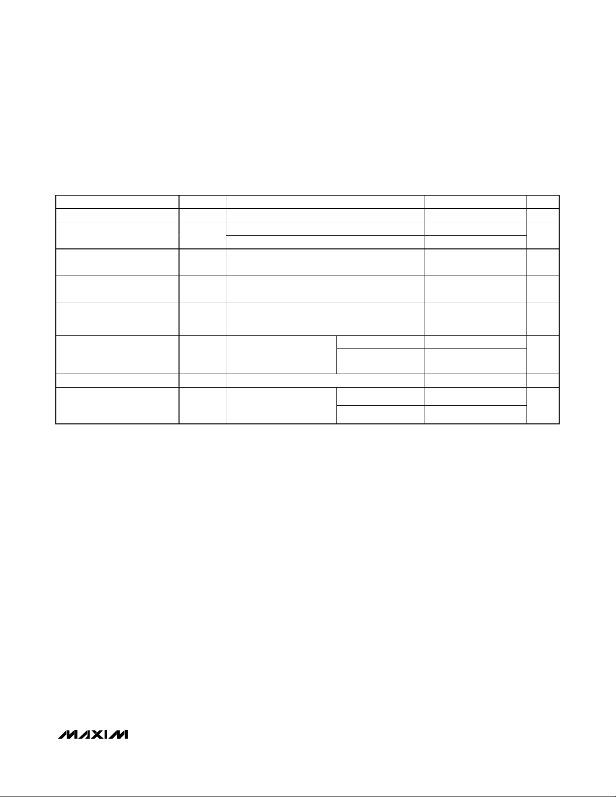
ELECTRICAL CHARACTERISTICS—Single-Supply, BTL Configuration
(VDD= 24V, VSS= V
SUB
= LGND = 0V, V
SHDN
= 3.3V, V
MID
= 12V, C
VDD
= 660µF, C
MID1
= 10µF, C
MID2
= 10µF, R1 = R2 = R3 =
10kΩ, C
SFT
= 0.47µF, C
OUT
= 1000µF, C
FB_1
= 150pF, C
FB_2
= 10pF, C
BOOT
= 0.1µF, C
REGP
= C
REGM
= 1µF, R
IN_
= 30.1kΩ, R
F1A
= 121kΩ, R
F1B
= 562kΩ, RF2= 681kΩ, R
REF
= 68kΩ, RL= ∞, TA= T
MIN
to T
MAX
, unless otherwise noted. Typical values are at TA=
+25°C.) (Note 2)
PARAMETER SYMBOL CONDITIONS MIN TYP MAX UNITS
Output Offset Voltage (Note 4) 7 mV
Power-Supply Rejection Ratio
(Note 4)
Continuous Output Power P
Efficiency
Total Harmonic Distortion Plus
Noise (Notes 6, 10, and 11)
Signal-to-Noise Ratio SNR
Shutdown-to-Full Operation t
Click-and-Pop K
PSRR
OUT
THD+N
SON
CP
VDD = 20V to 40V 88
= 24V + 500mV
V
DD
, f = 1kHz 77
P-P
RL = 8Ω, fIN = 1kHz, THD+N = 10%,
(Notes 6, 10, and 11)
R
= 8Ω, P
L
= 10W, THD+N = 10%,
OUT
(Notes 5 and 6)
fIN = 1kHz, BW = 22Hz to 22kHz,
= 8Ω, P
R
L
P
= 32W, RL = 8Ω,
OUT
BW = 22Hz to 22kHz
(Notes 6, 10, and 11)
P eak vol tag e, 32- sam p l es
OUT
= 10W
Unweighted 90
A-weighted 96
Into shutdown -47
p er second , A- w ei g hted
( N otes 4, 11, and 12)
Out of shutdown -32
32 W
83 %
0.08 %
68 ms
dB
dB
dBV
MAX9742
Single-/Dual-Supply, Stereo 16W,
Class D Amplifier with Differential Inputs
6 _______________________________________________________________________________________
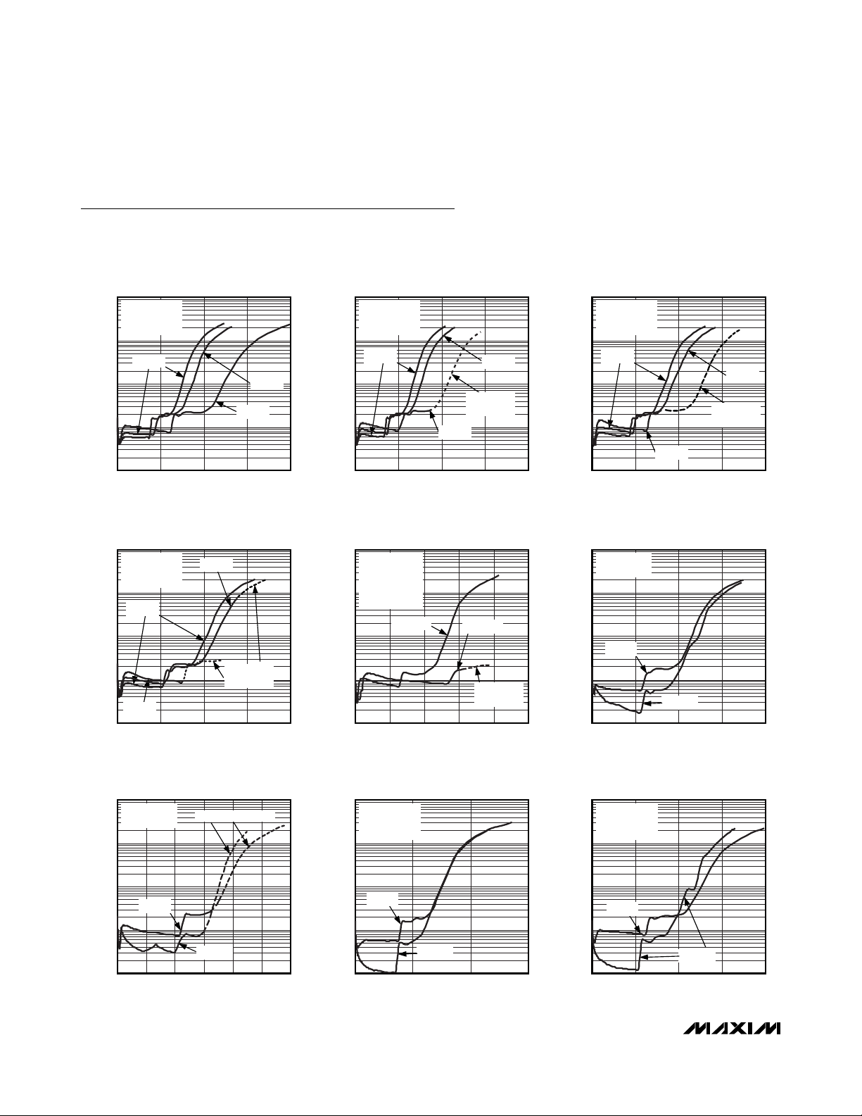
Typical Operating Characteristics
(24V single-supply mode, ±15V dual-supply mode, both channels driven in phase, THD+N measurement bandwidth = 22Hz to
22kHz, T
A
= +25°C, unless otherwise noted. See Figure 1 for test circuits, see
Typical Application Circuits/Functional Diagrams
for
test circuit component values.)
TOTAL HARMONIC DISTORTION
PLUS NOISE vs. OUTPUT POWER
MAX9742 toc01
OUTPUT POWER PER CHANNEL (W)
THD+N (%)
15105
0.1
1
10
100
0.01
020
SINGLE SUPPLY
V
DD
= 24V
f = 1kHz
RL = 8
Ω
RL = 6
Ω
RL = 4
Ω
TOTAL HARMONIC DISTORTION
PLUS NOISE vs. OUTPUT POWER
MAX9742 toc02
OUTPUT POWER PER CHANNEL (W)
THD+N (%)
302010
0.1
1
10
100
0.01
040
SINGLE SUPPLY
V
DD
= 32V
f = 1kHz
RL = 8
Ω
RL = 6
Ω
THERMALLY
LIMITED
RL = 4
Ω
TOTAL HARMONIC DISTORTION
PLUS NOISE vs. OUTPUT POWER
MAX9742 toc03
OUTPUT POWER PER CHANNEL (W)
THD+N (%)
302010
0.1
1
10
100
0.01
040
SINGLE SUPPLY
V
DD
= 36V
f = 1kHz
RL = 8
Ω
RL = 6
Ω
THERMALLY
LIMITED
RL = 4
Ω
TOTAL HARMONIC DISTORTION
PLUS NOISE vs. OUTPUT POWER
MAX9742 toc04
OUTPUT POWER PER CHANNEL (W)
THD+N (%)
302010
0.1
1
10
100
0.01
040
SINGLE SUPPLY
V
DD
= 40V
f = 1kHz
RL = 8
Ω
RL = 6
Ω
THERMALLY
LIMITED
RL = 4
Ω
TOTAL HARMONIC DISTORTION
PLUS NOISE vs. OUTPUT POWER
MAX9742 toc05
OUTPUT POWER (W)
THD+N (%)
302010
0.1
1
10
100
0.01
05040
BTL
CONFIGURATION
V
DD
= 24V
R
L
= 8
Ω
f = 1kHz
VDD = 24V
VDD = 36V
THERMALLY
LIMITED
TOTAL HARMONIC DISTORTION
PLUS NOISE vs. OUTPUT POWER
MAX9742 toc06
OUTPUT POWER PER CHANNEL (W)
THD+N (%)
15105
0.1
1
10
100
0.01
020
DUAL SUPPLY
R
L
= 8
Ω
f = 1kHz
f = 100Hz
TOTAL HARMONIC DISTORTION
PLUS NOISE vs. OUTPUT POWER
MAX9742 toc07
OUTPUT POWER PER CHANNEL (W)
THD+N (%)
2010
0.1
1
10
100
0.01
03015525
DUAL SUPPLY
R
L
= 4
Ω
f = 1kHz
f = 100Hz
THERMALLY LIMITED
TOTAL HARMONIC DISTORTION
PLUS NOISE vs. OUTPUT POWER
MAX9742 toc08
OUTPUT POWER PER CHANNEL (W)
THD+N (%)
105
0.1
1
10
100
0.01
015
SINGLE SUPPLY
V
DD
= 24V
R
L
= 8
Ω
f = 1kHz
f = 100Hz
TOTAL HARMONIC DISTORTION
PLUS NOISE vs. OUTPUT POWER
MAX9742 toc09
OUTPUT POWER PER CHANNEL (W)
THD+N (%)
105
0.1
1
10
100
0.01
02015
SINGLE SUPPLY
V
DD
= 24V
R
L
= 4
Ω
f = 1kHz
f = 100Hz
MAX9742
Single-/Dual-Supply, Stereo 16W,
Class D Amplifier with Differential Inputs
_______________________________________________________________________________________
7
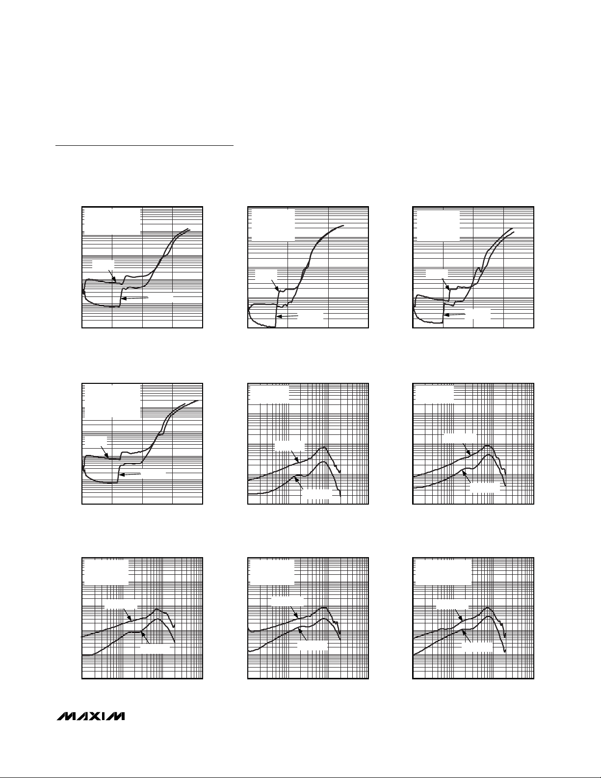
Typical Operating Characteristics (continued)
(24V single-supply mode, ±15V dual-supply mode, both channels driven in phase, THD+N measurement bandwidth = 22Hz to
22kHz, T
A
= +25°C, unless otherwise noted. See Figure 1 for test circuits, see
Typical Application Circuits/Functional Diagrams
for
test circuit component values.)
TOTAL HARMONIC DISTORTION
PLUS NOISE vs. OUTPUT POWER
100
BTL CONFIGURATION
= 24V
V
DD
Ω
= 8
R
L
10
1
f = 1kHz
THD+N (%)
0.1
0.01
0.001
04030
OUTPUT POWER (W)
f = 100Hz
2010
TOTAL HARMONIC DISTORTION
PLUS NOISE vs. OUTPUT POWER
100
BTL CONFIGURATION
= 24V
V
DD
Ω
= 8
R
L
10
T
= 40°C
A
MAX9742 toc10
MAX9742 toc13
TOTAL HARMONIC DISTORTION
PLUS NOISE vs. OUTPUT POWER
100
SINGLE SUPPLY
= 24V
V
DD
Ω
= 8
R
L
10
= 40°C
T
A
1
THD+N (%)
f = 1kHz
0.1
f = 100Hz
0.01
015
OUTPUT POWER PER CHANNEL (W)
TOTAL HARMONIC DISTORTION
PLUS NOISE vs. FREQUENCY
100
DUAL SUPPLY
Ω
= 8
R
L
10
TOTAL HARMONIC DISTORTION
PLUS NOISE vs. OUTPUT POWER
100
SINGLE SUPPLY
= 24V
V
MAX9742 toc11
THD+N (%)
105
DD
Ω
= 8
R
L
10
= 40°C
T
A
1
f = 1kHz
0.1
f = 100Hz
0.01
02015
OUTPUT POWER PER CHANNEL (W)
105
TOTAL HARMONIC DISTORTION
PLUS NOISE vs. FREQUENCY
100
DUAL SUPPLY
Ω
= 4
R
MAX9742 toc14
L
10
MAX9742 toc12
MAX9742 toc15
1
f = 1kHz
THD+N (%)
0.1
0.01
0.001
04030
f = 100Hz
2010
OUTPUT POWER (W)
TOTAL HARMONIC DISTORTION
PLUS NOISE vs. FREQUENCY
100
SINGLE SUPPLY
= 24V
V
DD
Ω
= 8
R
L
10
P
= 5W
1
THD+N (%)
0.1
0.01
0.001
100 100k
OUT
FREQUENCY (Hz)
P
= 3W
OUT
10k1k
MAX9742 toc16
1
THD+N (%)
0.1
0.01
100 100k
P
= 8W
OUT
FREQUENCY (Hz)
P
= 4W
OUT
10k1k
TOTAL HARMONIC DISTORTION
PLUS NOISE vs. FREQUENCY
100
SINGLE SUPPLY
= 24V
V
DD
Ω
= 4
R
L
10
P
= 9W
1
THD+N (%)
0.1
0.01
0.001
100 100k
OUT
P
FREQUENCY (Hz)
OUT
= 5W
10k1k
MAX9742 toc17
P
= 13W
1
THD+N (%)
0.1
0.01
100 100k
OUT
P
OUT
FREQUENCY (Hz)
= 8W
10k1k
TOTAL HARMONIC DISTORTION
PLUS NOISE vs. FREQUENCY
100
BTL CONFIGURATION
= 24V
V
DD
Ω
= 8
R
L
10
P
= 17W
1
THD+N (%)
0.1
0.01
0.001
100 100k
OUT
P
FREQUENCY (Hz)
OUT
= 12W
10k1k
MAX9742 toc18
MAX9742
Single-/Dual-Supply, Stereo 16W,
Class D Amplifier with Differential Inputs
8 _______________________________________________________________________________________
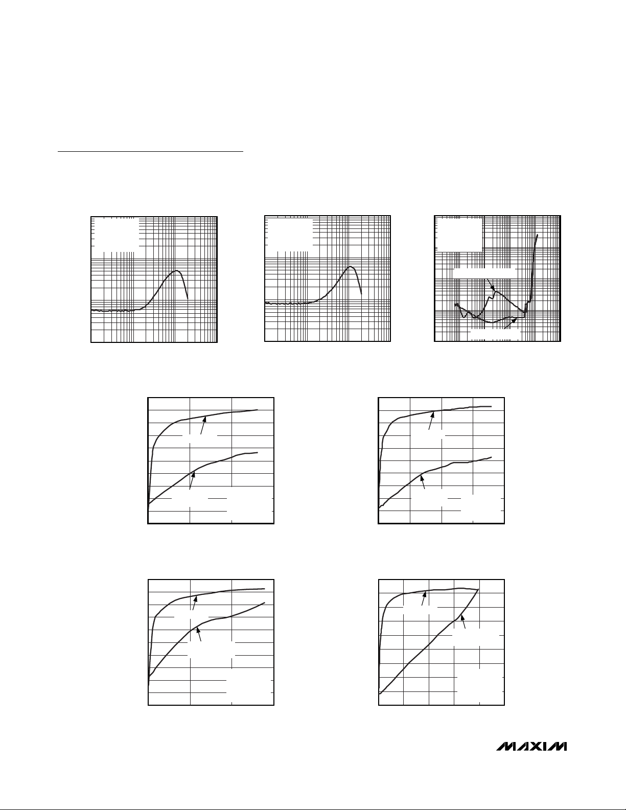
Typical Operating Characteristics (continued)
(24V single-supply mode, ±15V dual-supply mode, both channels driven in phase, THD+N measurement bandwidth = 22Hz to
22kHz, T
A
= +25°C, unless otherwise noted. See Figure 1 for test circuits, see
Typical Application Circuits/Functional Diagrams
for
test circuit component values.)
TOTAL HARMONIC DISTORTION
PLUS NOISE vs. FREQUENCY
10
SINGLE SUPPLY
= 24V
V
DD
Ω
= 8
R
1
THD+N (%)
0.1
P
L
OUT
= 50mW
MAX9742 toc19
10
1
THD+N (%)
0.1
TOTAL HARMONIC DISTORTION
PLUS NOISE vs. FREQUENCY
SINGLE SUPPLY
= 24V
V
DD
Ω
= 4
R
L
= 50mW
P
OUT
TOTAL HARMONIC DISTORTION PLUS NOISE vs.
OUTPUT POWER WITH AND WITHOUT T-NETWORK
100
SINGLE SUPPLY
= 24V
V
10
1
THD+N (%)
0.1
DD
Ω
= 8
R
L
f = 1kHz
WITHOUT T-NETWORK
MAX9742 toc20
MAX9742 toc21
0.01
100 100k
FREQUENCY (Hz)
10k1k
EFFICIENCY AND POWER
DISSIPATION vs. OUTPUT POWER
100
90
80
70
60
50
40
EFFICIENCY (%)
30
20
10
0
015
EFFICIENCY
SYSTEM POWER
DISSIPATION
510
OUTPUT POWER PER CHANNEL (W)
EFFICIENCY AND POWER
DISSIPATION vs. OUTPUT POWER
100
90
80
70
60
50
40
EFFICIENCY (%)
30
20
10
0
EFFICIENCY
SYSTEM POWER
DISSIPATION
015
510
OUTPUT POWER PER CHANNEL (W)
0.01
100 100k
MAX9742 toc22
SINGLE SUPPLY
= 30V
V
DD
Ω
= 8
R
L
= 1kHz
f
IN
MAX9742 toc24
SINGLE SUPPLY
= 24V
V
DD
= 8Ω
R
L
= 1kHz
f
IN
FREQUENCY (Hz)
5.0
4.5
4.0
3.5
3.0
2.5
2.0
1.5
POWER DISSIPATION (W)
1.0
0.5
0
2.5
2.0
1.5
1.0
POWER DISSIPATION (W)
0.5
0
10k1k
0.01
0.001 100
WITH T-NETWORK
0.10.01 101
OUTPUT POWER PER CHANNEL (W)
EFFICIENCY AND POWER
DISSIPATION vs. OUTPUT POWER
100
90
80
70
60
50
40
EFFICIENCY (%)
30
20
10
0
020
EFFICIENCY
SYSTEM POWER
DISSIPATION
51015
OUTPUT POWER PER CHANNEL (W)
MAX9742 toc23
DUAL SUPPLY
Ω
= 8
R
L
= 1kHz
f
IN
5.0
4.5
4.0
3.5
3.0
2.5
2.0
1.5
POWER DISSIPATION (W)
1.0
0.5
0
EFFICIENCY AND POWER
DISSIPATION vs. OUTPUT POWER
90
80
70
60
50
40
EFFICIENCY (%)
30
20
10
0
EFFICIENCY
025
5101520
OUTPUT POWER PER CHANNEL (W)
MAX9742 toc25
SYSTEM POWER
DISSIPATION
SINGLE SUPPLY
= 24V
V
DD
= 4Ω
R
L
= 1kHz
f
IN
9
8
7
6
5
4
3
POWER DISSIPATION (W)
2
1
0
MAX9742
Single-/Dual-Supply, Stereo 16W,
Class D Amplifier with Differential Inputs
_______________________________________________________________________________________
9
Typical Operating Characteristics (continued)
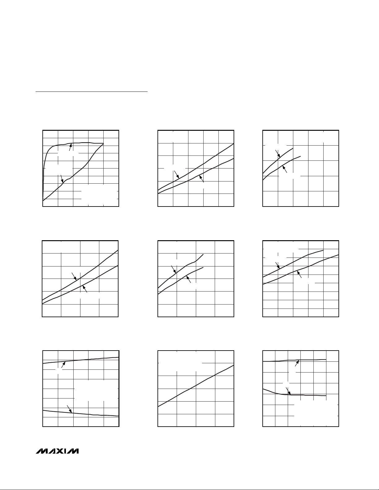
(24V single-supply mode, ±15V dual-supply mode, both channels driven in phase, THD+N measurement bandwidth = 22Hz to
22kHz, T
A
= +25°C, unless otherwise noted. See Figure 1 for test circuits, see
Typical Application Circuits/Functional Diagrams
for
test circuit component values.)
100
90
80
70
60
50
40
EFFICIENCY (%)
30
20
10
0
EFFICIENCY AND POWER
DISSIPATION vs. OUTPUT POWER
EFFICIENCY
SYSTEM POWER
DISSIPATION
BTL CONFIGURATION
V
DD
R
L
f
IN
050
10 20 30 40
OUTPUT POWER (W)
= 24V
Ω
= 8
= 1kHz
MAX9742 toc26
10
9
8
7
6
5
4
3
POWER DISSIPATION (W)
2
1
0
OUTPUT POWER PER CHANNEL (W)
30
25
20
15
10
5
0
±
DUAL SUPPLY
R
L
10
OUTPUT POWER
vs. SUPPLY VOLTAGE
30
SINGLE SUPPLY
Ω
= 8
R
L
25
20
15
10
OUTPUT POWER PER CHANNEL (W)
5
0
20 4035
10% THD+N
3025
SUPPLY VOLTAGE (V)
MAX9742 toc29
1% THD+N
30
SINGLE SUPPLY
R
L
25
10% THD+N
20
15
10
OUTPUT POWER PER CHANNEL (W)
5
0
20 4035
SUPPLY CURRENT
vs. SUPPLY VOLTAGE
20
15
10
5
0
-5
SUPPLY CURRENT (mA)
-10
-15
-20
I
DD
±10 ±20±18±14
DUAL SUPPLY
OUTPUT FILTER REMOVED
NO LOAD CONNECTED
= |VSS|
V
DD
I
SS
±16±12
SUPPLY VOLTAGE (V)
MAX9742 toc32
18
SINGLE SUPPLY
OUTPUT FILTER REMOVED
17
INPUTS GROUNDED
NO LOAD CONNECTED
16
15
14
SUPPLY CURRENT (mA)
13
12
20 4030
OUTPUT POWER
vs. SUPPLY VOLTAGE
Ω
= 8
10% THD+N
±
±
14
12
SUPPLY VOLTAGE (V)
OUTPUT POWER
vs. SUPPLY VOLTAGE
Ω
= 4
1% THD+N
SUPPLY VOLTAGE (V)
SUPPLY CURRENT
vs. SUPPLY VOLTAGE
SUPPLY VOLTAGE (V)
3025
OUTPUT POWER
vs. SUPPLY VOLTAGE
25
MAX9742 toc27
20
10% THD+N
15
1% THD+N
±
12
10
SUPPLY VOLTAGE (V)
1% THD+N
±
16
10
5
OUTPUT POWER PER CHANNEL (W)
0
±
±
20
18
±
OUTPUT POWER
vs. SUPPLY VOLTAGE
45
BTL CONFIGURATION
MAX9742 toc30
OUTPUT POWER (W)
40
35
30
25
20
15
10
Ω
= 8
R
L
10% THD+N
5
0
20 302824
SUPPLY VOLTAGE (V)
SHUTDOWN SUPPLY CURRENT
vs. SUPPLY VOLTAGE
10
MAX9742 toc33
3525
0
-10
-20
-30
SUPPLY CURRENT (nA)
-40
-50
-60
±10 ±22±18 ±20±12 ±16
I
SS
±14
SUPPLY VOLTAGE (V)
±
±
14
16
1% THD+N
2622
I
DD
DUAL SUPPLY
= |VSS|
V
DD
OUTPUT FILTER REMOVED
INPUTS GROUNDED
NO LOAD CONNECTED
DUAL SUPPLY
Ω
= 4
R
L
±
18
MAX9742 toc28
±
20
MAX9742 toc31
MAX9742 toc34
MAX9742
Single-/Dual-Supply, Stereo 16W,
Class D Amplifier with Differential Inputs
10 ______________________________________________________________________________________
Typical Operating Characteristics (continued)
(24V single-supply mode, ±15V dual-supply mode, both channels driven in phase, THD+N measurement bandwidth = 22Hz to
22kHz, T
A
= +25°C, unless otherwise noted. See Figure 1 for test circuits, see
Typical Application Circuits/Functional Diagrams
for
test circuit component values.)
SHUTDOWN SUPPLY CURRENT
vs. SUPPLY VOLTAGE
1.0
SINGLE SUPPLY
INPUTS AC GROUNDED
NO LOAD CONNECTED
0.8
0.6
0.4
SUPPLY CURRENT (mA)
0.2
0
-20
MAX9742 toc35
-40
-60
-80
OUTPUT AMPLITUDE (dBV)
-100
WIDEBAND OUTPUT SPECTRUM
RBW = 10kHz
MEASURED AT SINGLEENDED FILTER OUTPUT
INPUTS AC GROUNDED
OUTPUT SPECTRUM FFT
0
SINGLE SUPPLY
Ω
= 8
R
L
-20
= 1kHz
MAX9742 toc36
f
IN
= -60dBV
V
OUT_
-40
-60
-80
OUTPUT AMPLITUDE (dBV)
-100
MAX9742 toc37
0
20 4025 35
SUPPLY VOLTAGE (V)
POWER-SUPPLY REJECTION RATIO
vs. FREQUENCY
0
DUAL SUPPLY
Ω
= 8
R
L
-10
-20
-30
-40
PSRR (dB)
-50
VSS = -15V + 500mV
-60
-70
-80
10 100k100
FREQUENCY (Hz)
CROSSTALK vs. FREQUENCY
0
DUAL SUPPLY
-10
= 8Ω
R
L
= 1W
P
OUT
-20
-30
-40
-50
CROSSTALK (dB)
-60
-70
-80
-90
R INTO L
L INTO R
10 100k100
FREQUENCY (Hz)
30
P-P
VDD = 15V + 500mV
1k 10k
1k 10k
MAX9742 toc39
-120
0 20k5k
FREQUENCY (Hz)
POWER-SUPPLY REJECTION RATIO
vs. FREQUENCY
0
BTL
-10
= 24V + 500mV
V
-20
-30
-40
-50
PSRR (dB)
-60
-70
-80
-90
-100
DD
Ω
RL = 8
10 100k100
P-P
FREQUENCY (Hz)
10k 15k
MAX9742 toc40
1k 10k
-120
0.1 1001.0
FREQUENCY (MHz)
10
POWER-SUPPLY REJECTION RATIO
vs. FREQUENCY
20
SINGLE SUPPLY
= 24V + 500mV
V
DD
0
Ω
MAX9742 toc38
P-P
RL = 8
-20
-40
PSRR (dB)
-60
-80
-100
-120
10 100k
P-P
OUT_ PSRR
MID PSRR
10k1k100
FREQUENCY (Hz)
EXITING SHUTDOWN
MAX9742 toc41
CROSSTALK vs. FREQUENCY
20
SINGLE SUPPLY
= 8Ω
R
L
0
= 1W
P
OUT
-20
-40
-60
CROSSTALK (dB)
-80
-100
-120
10 100k
R INTO L
L INTO R
FREQUENCY (Hz)
DUAL SUPPLY
V
SHDN
2V/div
V
OUT_
20V/div
V
OUT_
5V/div
R
MAX9742 toc42
FILTERED
10k1k100
= 8Ω
L
(DUAL SUPPLY)
20ms/div
MAX9742 toc43
MAX9742
Single-/Dual-Supply, Stereo 16W,
Class D Amplifier with Differential Inputs
______________________________________________________________________________________
11
Typical Operating Characteristics (continued)
(24V single-supply mode, ±15V dual-supply mode, both channels driven in phase, THD+N measurement bandwidth = 22Hz to
22kHz, T
A
= +25°C, unless otherwise noted. See Figure 1 for test circuits, see
Typical Application Circuits/Functional Diagrams
for
test circuit component values.)
ENTERING SHUTDOWN
DUAL SUPPLY
= 8Ω
R
L
V
SHDN
2V/div
V
OUT_
20V/div
FILTERED
V
OUT_
5V/div
10ms/div
CASE TEMPERATURE
vs. OUTPUT POWER
50
40
30
20
CASE TEMPERATURE (°C)
10
0
012462
OUTPUT POWER PER CHANNEL (W)
MAX9742 toc44
SINGLE SUPPLY
= 24V
V
DD
= 8Ω
R
L
4-LAYER PCB
810
FILTERED
MAX9742 toc47
V
SHDN
2V/div
V
OUT_
10V/div
V
OUT_
5V/div
CASE TEMPERATURE (°C)
120
100
80
60
40
20
0
0205
EXITING SHUTDOWN
SINGLE SUPPLY
= 8Ω
R
L
20ms/div
CASE TEMPERATURE
vs. OUTPUT POWER
SINGLE SUPPLY
= 24V
V
DD
= 4Ω
R
L
4-LAYER PCB
10 15
OUTPUT POWER PER CHANNEL (W)
ENTERING SHUTDOWN
MAX9742 toc45
V
SHDN
2V/div
V
OUT_
10V/div
FILTERED
V
OUT_
5V/div
(SINGLE SUPPLY)
SINGLE SUPPLY
R
10ms/div
= 8Ω
L
OUTPUT WAVEFORM
SINGLE SUPPLY, VDD = 24V
V
OUT
10V/div
V
OUTR
10V/div
INPUTS AC GROUNDED
1µs/div
MAX9742 toc48
MAX9742 toc46
MAX9742 toc49
EMI AMPLITUDE vs. FREQUENCY
40
SINGLE SUPPLY
= 8Ω, P
OUT
18.1dBµV/m
BELOW LIMIT
100
FREQUENCY (MHz)
= 1.25W
EN55022B LIMIT
12.8dBµV/m
BELOW LIMIT
R
L
35
SPEAKER CABLE
LENTH = 1m
30
9.4dBµV/m BELOW LIMIT
25
20
AMPLITUDE (dBµV/m)
15
10
5
30 1000
MAX9742 toc50
AMPLITUDE (dBµV/m)
EMI AMPLITUDE vs. FREQUENCY
40
SINGLE SUPPLY
= 4Ω, P
R
L
35
SPEAKER CABLE
LENTH = 1m
30
25
7dBµV/m
20
BELOW
LIMIT
15
10
5
30 1000
= 1.25W
OUT_
11.3dBµV/m
BELOW LIMIT
100
FREQUENCY (MHz)
MAX9742 toc51
EN55022B LIMIT
7.8dBµV/m
BELOW LIMIT
5.8dBµV/m
BELOW LIMIT
3.6dBµV/m
BELOW LIMIT

MAX9742
Single-/Dual-Supply, Stereo 16W,
Class D Amplifier with Differential Inputs
12 ______________________________________________________________________________________12 ______________________________________________________________________________________
Pin Description
PIN NAME FUNCTION
1, 6, 18,
27, 28, 36
2, 3 OUTL Left Speaker Output
4 SUB Device Substrate. Connect SUB to VSS.
5 BOOTL Left-Channel Bootstrap Capacitor Terminal. Connect a 0.1µF capacitor between BOOTL and OUTL.
7 INL+ Left-Channel Positive Input
8 INL-
9 FBL
10 REGM
11 MID
12 REGP
N.C. No Connection. Not internally connected.
Left-Channel Negative Input. Connect an external feedback capacitor between INL- and FBL. See the
Feedback Capacitor (C
Left-Channel Feedback Capacitor Terminal. Connect an external feedback capacitor between FBL and
INL-. See the Feedback Capacitor (C
-5V Internal Regulator Output. Regulator output voltage is with respect to MID. Bypass REGM with a 1µF
capacitor to signal ground plane (SGND). See the Supply Bypassing/Layout section.
Midsupply Bias Voltage Input. The MID input biases the internal preamplifiers to the average value of the
and VSS supply inputs. For dual-supply operation, connect to the signal ground plane (SGND). For
V
DD
single-supply operation, apply a voltage to MID equal to 0.5 x V
divider and decoupling network (see the Setting V
Circuits/Functional Diagrams and Supply Bypassing/Layout sections.
5V Internal Regulator Output. Regulator output voltage is with respect to MID. Bypass REGP with a 1µF
capacitor to the signal ground plane (SGND). See the Supply Bypassing/Layout section.
) section.
FB_
FB_
) section.
through an external resistive voltage-
section). See the Typical Application
MID
DD
Reference Current Resistor Terminal. Connect an external resistor from REFCUR to REGP to set the
13 REFCUR
14 SFT
15 LGND
16 LV
17 SHDN
19 FBR
20 INR-
21 INR+ Right-Channel Positive Input
22 NSENSE
23 REGLS
switching frequency and output short-circuit current-limit value. Use resistor values greater than or equal
to 58kΩ and less than or equal to 75kΩ. See the Setting the Switching Frequency and Output Current
Limit (R
Soft-Start Capacitor Terminal/Mute Input. Connect a 0.22µF capacitor between SFT and PGND to utilize
the soft-start power-up sequence. Drive SFT low to mute the outputs.
Logic Ground. Connect LGND to signal ground (SGND) and power ground (PGND) planes. See the
Supply Bypassing/Layout section.
Internal 5V Logic Supply. Bypass LVDD to LGND with a 0.1µF capacitor.
DD
Active-Low Shutdown Input. Drive SHDN high for normal operation. Drive SHDN low to place the device
into shutdown mode.
Right-Channel Feedback Capacitor Terminal. Connect an external feedback capacitor between FBR and
INR-. See the Feedback Capacitor (C
Right-Channel Negative Input. Connect an external feedback capacitor between INR- and FBR. See the
Feedback Capacitor (C
Negative Supply Sense Input. NSENSE is internally connected to V
between NSENSE and REGLS.
7V Internal Regulator Output. REGLS output voltage is with respect to V
capacitor to NSENSE.
REF
) section.
FB_
) section.
) section.
FB_
. Connect a 1µF bypass capacitor
SS
. Bypass REGLS with a 1µF
SS

MAX9742
Single-/Dual-Supply, Stereo 16W,
Class D Amplifier with Differential Inputs
______________________________________________________________________________________ 13
Detailed Description
The MAX9742 is a two-channel, single-ended Class D
stereo amplifier capable of providing 16W of output
power on each channel into 4Ω loads in single- or dualsupply operation. The amplifier can also provide 32W
of output power in a mono bridge-tied-load (BTL) configuration. The device offers Class AB audio performance with Class D efficiency.
The differential input architecture reduces commonmode noise pickup. The device can also be configured
for single-ended input signals.
The connection of external feedback components
allows custom gain settings.
Class D Operation and Efficiency
Class D amplifiers are switch-mode devices capable of
significantly higher power efficiencies in comparison to
linear amplifiers. The output stage of the MAX9742 consists of a half-bridge speaker driver (see Figure 2). The
high efficiency of a Class D amplifier is attributed to the
region of operation of the output stage transistors. In a
Class D amplifier, the output transistors act as currentsteering switches by switching the output between V
DD
and VSS(ground for single-supply operation). Any
power loss associated with the Class D output stage is
mostly due to the I2R loss of the MOSFET on-resistance
and quiescent current overhead. The theoretical best
______________________________________________________________________________________ 13
Pin Description (continued)
Figure 1. Test Circuits for Single-Ended and BTL Configurations
Test Circuits
PIN NAME FUNCTION
24 BOOTR Right-Channel Bootstrap Capacitor. Connect a 0.1µF capacitor between BOOTR and OUTR.
25, 26 OUTR Right Speaker Output
29, 30,
34, 35
31, 32, 33 V
EP EP
OUTL
MAX9742
OUTR
V
DD
SS
Positive Power-Supply Input. Bypass VDD to LGND with a 0.1µF plus additional bulk capacitance. See
the Supply Pumping Effects section.
Negative Power-Supply Input. For dual-supply operation, connect to negative power-supply voltage
and bypass V
to LGND with a 0.1µF plus additional bulk capacitance. For single-supply operation,
SS
connect to LGND.
Exposed Paddle. EP is internally connected to device substrate. Connect EP to V
SS
section of copper to maximize power dissipation.
SINGLE-ENDED CONFIGURATION
L
F
+
+
C
F
L
F
R
L
AUX-0025
FILTER
-
+
AUDIO
ANALYZER
-
+
C
F
R
L
-
-
through a large
BTL CONFIGURATION
L
OUTL
MAX9742
OUTR
NOTE: SINGLE-ENDED CONFIGURATION IS AC-COUPLED IN SINGLE-SUPPLY MODE.
F
C
F
C
F
L
F
+
AUX-0025
R
L
FILTER
-
+
AUDIO
ANALYZER
-

MAX9742
Single-/Dual-Supply, Stereo 16W,
Class D Amplifier with Differential Inputs
14 ______________________________________________________________________________________
efficiency of a linear amplifier is 78%; however, that efficiency is only exhibited at peak output powers. Under
normal operating levels (typical music reproduction levels), efficiency falls below 30%, whereas the MAX9742
still exhibits 80% efficiency under the same conditions.
Since the output transistors switch the output to either
V
DD
or VSS(ground for single-supply operation), the
resulting output of a Class D amplifier is a high-frequency square wave. This square wave is pulse-widthmodulated by the audio input signal. In the MAX9742,
the pulse-width modulation (PWM) is accomplished by
comparing the input audio signal to an internally generated triangle wave oscillator. The resulting duty cycle of
the square wave is proportional to the level of the input
signal. When the input signal is at 0V, the duty cycle of
the MAX9742 output is equal to 50%. To extract the
amplified audio signal from this PWM waveform, the
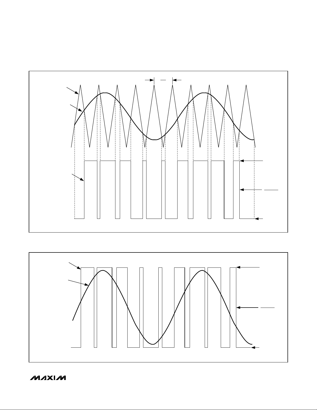
output of the MAX9742 is fed to an external LC lowpass
filter (see the
Single-Ended LC Output Filter Design (L
F
and CF)
section). The LC filter works as an averaging
circuit for the PWM output voltage waveform. The
resulting averaged output voltage is equal to the amplified audio signal. Figure 3a illustrates the resulting
PWM output waveform due to the varying input signal
level, and Figure 3b shows the recovered amplified
input signal after filtering.
Figure 2. Simplified Block Diagram of the MAX9742 Output Stage
C
NSENSE
(INTERNALLY
CONNECTED TO V
MAX9742
REGLS
1µF
)
SS
7V REGULATOR
(WITH RESPECT TO V
GATE DRIVE LOGIC
REGLS
D
BOOT
1N4148
SS
C
BOOT
0.1µF
V
DD
)
OUT_
V
REGLS
L
F
C
F
V
SS
DUAL-SUPPLY CONFIGURATION SHOWN
V
SS
MAX9742
Single-/Dual-Supply, Stereo 16W,
Class D Amplifier with Differential Inputs
______________________________________________________________________________________ 15
Figure 3a. MAX9742 Output with an Applied Input Signal
Figure 3b. MAX9742 Output with Resulting Output After Filtering
INTERNAL TRIANGLE
WAVE OSCILLATOR
INPUT
SIGNAL
V
OUT_
NOTE: FOR CLARITY, SIGNAL PERIODS ARE NOT SHOWN TO ACTUAL SCALE.
1
f
SW
V
DD
VDD + V
SS
2
V
SS
V
OUT_
AVERAGE VALUE
OF V
OUT_
NOTE: FOR CLARITY, SIGNAL PERIODS ARE NOT SHOWN TO ACTUAL SCALE.
V
DD
VDD + V
2
V
SS
SS

MAX9742
Single-/Dual-Supply, Stereo 16W,
Class D Amplifier with Differential Inputs
16 ______________________________________________________________________________________
Shutdown Mode
The MAX9742 features a low-power shutdown mode
that reduces quiescent current consumption to less
than 0.5mA in single-supply mode and less than 1µA in
dual-supply mode. Drive SHDN low to place the device
into shutdown mode. Connect SHDN to a logic-high for
normal operation.
The maximum voltage that may be applied to the SHDN
input is 4V (see the
Absolute Maximum Ratings
sec-
tion). If the SHDN input must be controlled by a 5V
logic signal, limit the maximum voltage that can be
applied to the SHDN input to 4V through an external
resistive divider.
Click-and-Pop Suppression
The MAX9742 features comprehensive click-and-pop
suppression that minimizes audible transients on startup and shutdown. While in shutdown, the half-bridge
output transistor switches are turned off, causing each
output to go high impedance. During startup, or powerup, the input amplifiers are muted and an internal loop
sets the modulator bias voltages to the correct levels,
minimizing audible clicks and pops when the output
half-bridge is enabled. The value of the soft-start
capacitor, C
SFT
, affects the click-and-pop performance
and startup time of the MAX9742 (see the
Soft-Start
Capacitor (C
SFT)
section). To maximize click-and-pop
suppression when powering up an audio system, drive
SHDN or SFT (see the
Mute Function
section) to 0V
until the rest of the circuitry in the system has had
enough time to stabilize. This ensures the MAX9742 is
the last device to be activated in the system and prevents transients caused by circuitry preceding the
MAX9742 from being amplified at the outputs.
Mute Function
The MAX9742 features a clickless/popless mute mode.
When the device is muted, the outputs stop switching,
muting the speaker. The mute function only affects the
output stage and does not shutdown the device. To
mute the MAX9742, drive SFT to ground. Figure 4
shows how an external transistor (MOSFET or BJT) can
be used to easily mute the MAX9742.
Thermal-Overload Protection
Thermal-overload protection limits total power dissipation in the MAX9742. When the junction temperature
exceeds approximately +160°C, the thermal protection
circuitry disables the amplifier output stage. The amplifiers are enabled once the junction temperature cools
by approximately 15°C. This results in a pulsing output
under continuous thermal-overload conditions.
Supply Undervoltage and
Overvoltage Protection
The MAX9742 features an undervoltage protection
function that prevents the device from operating if V
DD
is less than +7V with respect to V
MID
input or if VSSis
greater than -7V with respect to V
MID
. This feature prevents improper operation when insufficient supply voltages are present. Once the supply voltage exceeds the
undervoltage threshold, the MAX9742 is turned on and
the amplifiers are powered, provided that SHDN is high
and the outputs are unmuted.
The MAX9742 also features an overvoltage protection
function that prevents the device from operating if the
potential difference between VDDand VSSexceeds
+46V. This feature prevents the MAX9742 from damaging itself due to excessive supply pumping effects (see
the
Supply Pumping Effects
section). The device
returns to normal operation once the potential difference between VDDand VSSdrops below +46V.
Applications Information
Output Dynamic Range
Dynamic range is the difference between the noise
floor of the system and the output level at 10% THD+N.
It is essential that a system’s dynamic range be known
before setting the maximum output gain. Output clipping occurs if the output signal is greater than the
dynamic range of the system.
Use the THD+N vs. Output Power graph in
Typical
Operating Characteristics
to identify the system’s
dynamic range. Given the system’s supply voltage, find
the output power that causes 10% THD+N for a given
load. Use the following equation to determine the peak-
Figure 4. MAX9742 Mute Circuit
UN-MUTE
MUTE
10kΩ
C
SFT
SFT
LOGIC/POWER-UP
CONTROL
SEQUENCING
MAX9742
TO
OUTPUT
STAGE
MAX9742
Single-/Dual-Supply, Stereo 16W,
Class D Amplifier with Differential Inputs
______________________________________________________________________________________ 17
to-peak output voltage that causes 10% THD+N for a
given load.
where P
OUT_10%
is the output power that causes 10%
THD+N, RLis the load resistance, and V
OUT_P-P
is the
peak-to-peak output voltage. Determine the voltage
gain (A
V
) necessary to attain this output voltage based
on the maximum peak-to-peak input voltage (V
IN_P-P
):
Set the closed-loop voltage gain of the MAX9742 less
than or equal to AVto prevent clipping of the output,
unless audible clipping is acceptable for the application.
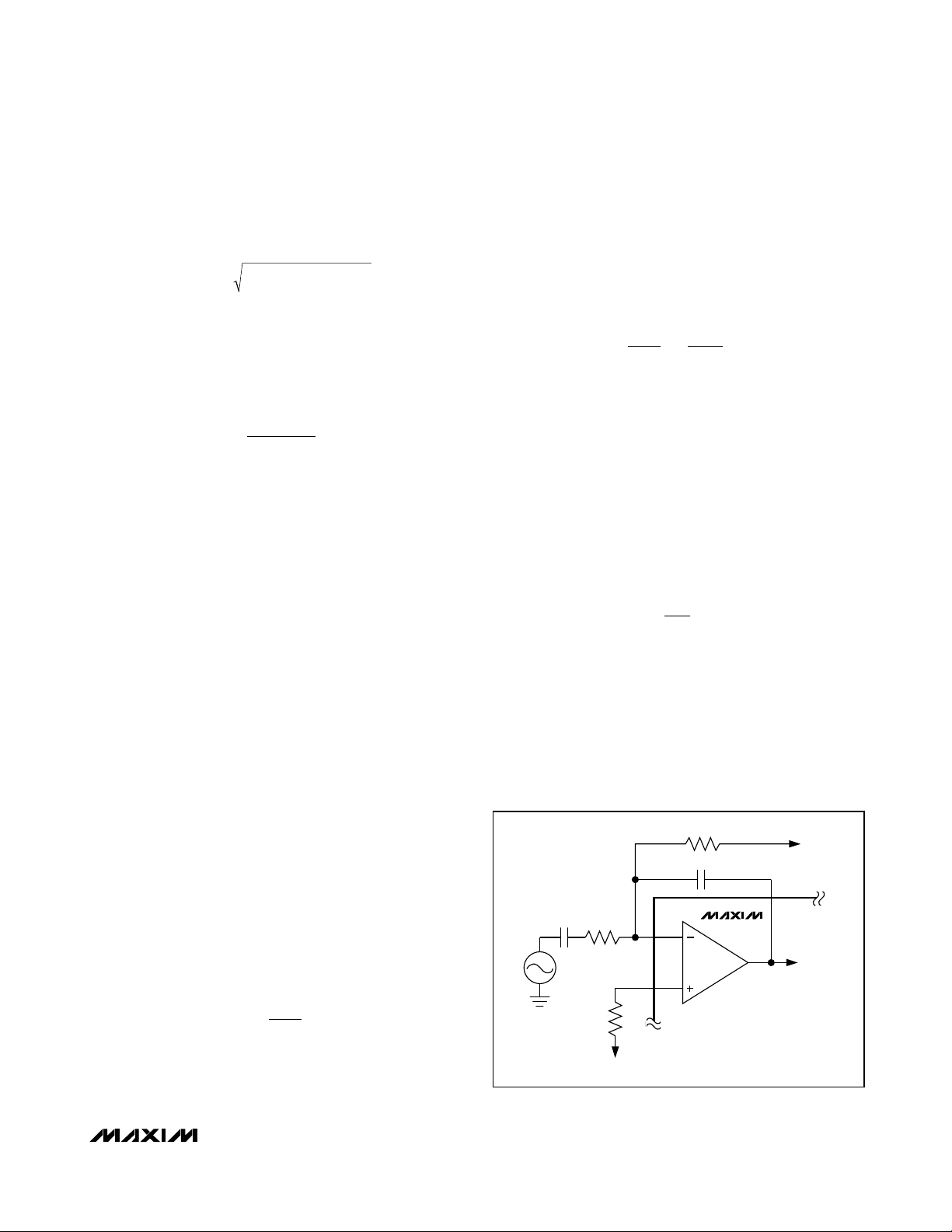
Input Amplifier
The external feedback networks of the MAX9742 input
amplifiers allow custom gain settings while maximizing
dynamic range. The input amplifiers also accommodate
a variety of standard amplifier configurations including
differential input, single-ended input, and summing
amplifiers. Due to the output current limitations of the
internal input amplifiers, always select feedback resistors
(RF1, see the
Typical Application Circuits/Functional
Diagrams
) with values greater than or equal to 400kΩ. To
preserve gain accuracy, avoid using feedback resistors
with values greater than 1MΩ. For proper operation, limit
common-mode input voltages to ±3V.
Differential Input Configuration
The
Typical Application Circuits/Functional Diagrams
show each channel of the MAX9742 configured as differential input amplifiers. A differential input offers
improved noise immunity over a single-ended input. In
systems that include high-speed digital circuitry, highfrequency noise can couple into the amplifier’s input
traces. The signals appear at the amplifier’s inputs as
common-mode noise. A differential input amplifier
amplifies the difference of the two inputs, and signals
common to both inputs are subtracted out. When configured for differential inputs, the voltage gain of the
MAX9742 is set by:
where A
V
is the desired voltage gain in V/V. R
IN1
should be equal to R
IN2
, and RF1should be equal to
R
F2
.
When using the differential input configuration, the
common-mode rejection ratio (CMRR) is primarily limited by the external resistor tolerances. Ideally, to
achieve the highest possible CMRR, the resistors
should be perfectly matched and the following condition should be met:
To ensure the MAX9742 input amplifiers operate as
fully differential integrators, connect a capacitor
between IN_+ and MID whose value is equal to C
F
(see
the
Feedback Capacitor (CFB_)
section).
Single-Ended Input
Each channel of the MAX9742 can be configured as a
single-ended input amplifier by connecting IN_+ to MID
(through an external resistor, R
OS
) and driving IN_- with
the input source (see Figure 5). In this configuration,
the MAX9742 is configured as a single-ended amplifier
whose voltage gain is equal to:
where A
V
is the desired voltage gain in V/V.
To minimize output offset voltages due to input bias currents, connect a resistor, ROS, (see Figure 5) between
IN_+ and MID. Select the value of ROSso that the DC
resistances looking out of inputs of the amplifier (IN_+
and IN_-) are equal. For example, when using the dualsupply configuration with a DC-coupled input source, the
value of ROSshould be equal to RF||RIN.
Figure 5. Single-Ended Input Configuration
V2 2PR
OUT_P P OUT_10% L−
=×
()V
()
V
OUT_P P
A
(/)=
V
V
IN_P P
−
VV
−
R
A
V
F1
= ( / )VV
R
IN1
R
F1
R
IN1
=
R
F2
R
IN2
R
F
R
IN
A
(/)= − VV
V
R
F
C
FB_
C
IN
R
IN
V
IN
R
OS
IN_-
IN_+
MAX9742
FB_
OUT_
TO CLASS D
MODULATOR
MID

MAX9742
Single-/Dual-Supply, Stereo 16W,
Class D Amplifier with Differential Inputs
18 ______________________________________________________________________________________
Summing Configuration (Audio Mixer)
Figure 6 shows the MAX9742 configured as a summing
amplifier, which allows multiple audio sources to be linearly mixed together. Using this configuration, the output of the MAX9742 is equal to the weighted sum of the
input signals:
As shown in the above equation, the weighting or
amount of gain applied to each input signal source is
determined by the ratio of R
F
and the respective input
resistor (R
IN1
, R
IN2
, R
IN3
) connected to each signal
source. Select R
F
and R
IN_
so that the dynamic range
of the MAX9742 is not exceeded when the input signals
are at their maximum values and in phase with each
other (see the
Output Dynamic Range
section).
To minimize output offset voltages due to input bias
currents, connect a resistor, ROS, (see Figure 6)
between IN_+ and MID. Select the value of ROSsuch
that the DC resistances looking out of inputs of the
amplifier (IN_+ and IN_-) are equal. For example, when
using the dual-supply configuration with a DC-coupled
input source, the value of ROSshould be equal to
RF||R
IN1
||R
IN2
|| ||R
INn
.
Mono Bridge-Tied-Load (BTL)
Configuration
The MAX9742 also accommodates a mono bridge-tiedload (BTL) configuration that can be used in singlesupply and dual-supply applications. In the BTL
configuration, the speaker load is driven differentially
by connecting the half-bridge outputs as a full H-bridge
driver. To drive the speaker differentially, the inputs of
both channels must be driven by the same audio signal
with one channel 180° out-of-phase with the other
channel. Figure 7 shows the connections required for
BTL operation.
The advantages of BTL operation include reduced
component count due to the elimination of the outputcoupling capacitors when using single-supply operation, a 6dB increase in gain due to the load being
driven differentially, increased output power into a single load, and the minimization of the supply-pumping
since each half bridge is driven 180° out-of-phase (see
the
Supply Pumping Effects
section). For single-supply
applications, the output-coupling capacitors are not
needed for BTL operation since the DC voltage present
at each half-bridge output is equal in value and applies
to each side of the load. This means no DC voltage
appears across the load, and therefore, no DC current
flows into the speaker.
Figure 6. Summing Amplifier Configuration
R
V (V
= − ++
OUT_ IN1
F
R
IN1
V
IN2
R
R
IN2
F
V
IN3
R
F
)
R
IN3
R
F
C
FB_
C
IN
R
IN1
OUT_
(V
MAX9742
IN1
R
R
IN1
F
× V
IN2
R
C
IN
R
V
IN1
V
IN2
V
IN3
IN2
C
IN
R
IN3
R
OS
MID
IN_-
IN_+
V
R
F
IN2
FB_
× V
OUT_
TO CLASS D
MODULATOR
R
F
)
IN3
R
IN3

MAX9742
Single-/Dual-Supply, Stereo 16W,
Class D Amplifier with Differential Inputs
______________________________________________________________________________________ 19
Since each half-bridge output stage is only capable of
driving loads as small as 4Ω and each half-bridge sees
half of the differential load resistance when configured
for BTL, only use the BTL configuration with loads
greater than or equal to 8Ω. The MAX9742 may be thermally limited when using the BTL configuration with
high supply voltages due to the decreased load resistance seen by each half bridge. For optimum performance, the PCB should be thermally optimized to
achieve the continuous output powers required for the
application (see the
Thermal Considerations
section).
Component Selection
Feedback Capacitor (C
FB_
)
To maximize dynamic range, an external feedback
capacitor (C
FB_
) is needed to generate an error signal
for the Class D modulator. The feedback capacitor configures the input amplifier stage as an integrator whose
output is equal to an error signal consisting of the sum
of the integrated input audio and PWM output signals.
The integrator provides a noise-shaping function for the
closed-loop response of the amplifier.
Figure 7. Input Signal Source and Load Connections for BTL Operation
C
DIFFERENTIAL
AUDIO INPUT
C
C
C
IN
R
IN1
IN
R
IN2
C
F
MID
C
F
IN
R
IN2
IN
R
IN1
INL-
INL+
R
F2
R
F2
INR+
INR-
C
FBL
MAX9742
FBL
R
F1
MODULATOR
AND GATE DRIVE
MODULATOR
AND GATE DRIVE
V
DD
L
CLASS D
CLASS D
OUTL
V
SS
V
DD
OUTR
F
C
ZBL
C
F
R
ZBL
R
ZBL
C
F
C
L
F
ZBL
V
DD
VDD/2
/2
0V
V
OUT_P-P
V
OUT_P-P
2 x V
OUT_P-P
FBR
R
F1
A
= 2 ×
V_BTL
= R
R
IN1
IN2
R
R
IN_
, RF1 = R
C
FBR
F_
F2
V
SS

MAX9742
Single-/Dual-Supply, Stereo 16W,
Class D Amplifier with Differential Inputs
20 ______________________________________________________________________________________
To guarantee stability and minimize distortion, select
the external feedback resistor (RF_) and capacitor
(C
FB_
) so that the following conditions are met:
where f
SW
is the output switching frequency deter-
mined by R
REF
(see the
Setting the Switching
Frequency and Output Current Limit (R
REF
)
section).
Setting the Switching Frequency and
Output Current Limit (R
REF
)
Resistor R
REF
determines the output switching frequency
(f
SW
) and the output short-circuit current-limit value (ISC).
Set fSWand ISCwith the following equations:
For example, selecting a 68kΩ resistor for R
REF
results
in a switching frequency of 303kHz and an output
short-circuit current limit of 4.5A.
To prevent damage to the MAX9742 during output
short-circuit conditions and to utilize its full output
power capabilities, use resistor values greater than or
equal to 58kΩ and less than or equal to 75kΩ for R
REF
.
Input-Coupling Capacitor
The AC-coupling capacitors (CIN) and input resistors
(R
IN_
) form highpass filters that remove any DC bias
from an input signal (see the
Typical Application
Circuits/Functional Diagrams
). CINprevents any DC
components from the input-signal source from appearing at the amplifier outputs. The -3dB point of the highpass filter, assuming zero source impedance due to the
input signal source, is given by:
Choose C
IN
so that f
-3dB
is well below the lowest frequen-
cy of interest. Setting f
-3dB
too high affects the amplifier’s
low-frequency response. Use capacitors with low-voltage
coefficient dielectrics. Aluminum electrolytic, tantalum, or
film dielectric capacitors are good choices for AC-coupling capacitors. Capacitors with high-voltage coefficients, such as ceramics (non-C0G dielectrics), can
result in increased distortion at low frequencies.
Single-Ended LC Output Filter Design (LFand CF)
An LC output filter is needed to extract the amplified
audio signal from the PWM output (see Figure 8). The LC
circuit forms an LCR lowpass filter (neglecting voice coil
inductance) with the impedance of the speaker. To provide a maximally flat-frequency response, the LCR filter
should be designed to have a Butterworth response and
should be optimized for a specific speaker load. Table 1
provides some recommended standard L
F
and CFcom-
ponent values for 4Ω, 6Ω, and 8Ω speaker loads. The
component values given in Table 1 provide an approximate -3dB cutoff frequency (fC) of 40kHz. The following
paragraph provides information on calculating filter component values for cutoff frequencies other than 40kHz
and speaker loads not listed in Table 1.
The LCR filter has the following 2nd order transfer function:
where LFis the value of the filter inductor, CFis the
value of the filter capacitor, and R
SPKR
is the DC resistance of the speaker. The voice coil inductance of the
speaker has been neglected to simplify filter calculations (see the
Zobel Network
section). The above transfer function is presented in the general 2nd order
transfer function format given below:
where wnis the natural frequency in radians/s and ζ is
the damping ratio of the 2nd order system. For an ideal
Butterworth response, ζ is equal to 0.707 and ωCis
equal to the -3dB cutoff frequency, ωc. Using the above
transfer functions and converting to Hertz, the -3dB cutoff frequency of the filter is:
R C
× ≥ >
F_ FB_
21.5
f
SW
and R kF400 Ω
_
f
=
SW
3.3 s
=×
()
I 3.6A
SC
1
×
µ
68k
R
68k
R
REF
REF
Ω
()
Ω
Hz
A
f
=
3dB
−
2 R C
1
××
π
IN IN
()
Hz
1
×
L C
H
(s)
=
2
+
s
R C
FF
1
×
SPKR F F F
+
s
L C
2
ω
H
(s)
=
2
s2 s
+×× ×+
n
ζω ω
nn
f
=
C
2 L C
1
×× ×
π
FF
()
Hz
1
×
2

Using the transfer functions and the equation for fc, the
following expressions for LFand CFcan be derived:
Since the frequency response of the output filter is
dependent on the speaker resistance, it is best to optimize the LC filter for a particular load resistance. To
calculate the component values of the LC filter for a
given speaker load resistance, first select an appropriate cutoff frequency for the filter. The cutoff frequency
should be high enough so that upper audio frequency
band attenuation is kept to a minimum while providing
sufficient attenuation at the switching frequency (fSW) of
the MAX9742. Once the cutoff frequency is determined,
calculate C
F
using the DC resistance of the speaker
(R
SPKR
) and a damping ratio (ζ) equal to 0.707. Finally,
calculate L
F
using the resulting CFvalue.
When selecting C
F
, use capacitors with DC voltage rat-
ings greater than VDD.
When selecting L
F
, it is important to take into account
the DC resistance, current capabilities, and upper frequency limitations of the inductor. Choosing an inductor with minimum DC resistance minimizes I
2
R losses
due to the filter inductor and therefore preserves power
efficiency. The inductor current rating should be
greater than the maximum peak output current to prevent the inductor from going into saturation. Output
inductor saturation introduces nonlinearities into the
output signal and therefore increases distortion. The
upper frequency limit of the inductor should also be
taken into account. The load connected to the output of
the half-bridge (LC filter and speaker) should remain
inductive at the switching frequency of the MAX9742. If
not, a significant amount of high-frequency energy is
dissipated in the resistive load, therefore, increasing
the supply current to excessive levels. To prevent this
from occurring, select an output inductor whose selfresonant frequency is substantially higher than the
switching frequency of the MAX9742.
To minimize possible EMI radiation, place the LC filter
near the MAX9742 on the PCB.
Table 2 provides some suggested inductor manufacturers.
BTL LC Output Filter Design
When using the BTL configuration, optimize the output filter for fully differential operation (see Figure 9 and Table
3). Follow the design criteria provided for the singleended filter except use half the value of the BTL resistance for the output filter calculations. This is because
each half-bridge output sees half of the BTL resistance.
For example, with a BTL resistance of 8Ω the ideal filter
component values are CF= 0.7µF and LF= 22.5µH for a
maximally flat differential filter response with an approximate cutoff frequency of 40kHz. Rounding to the nearest
standard component values yields C
F
= 0.68µF and LF=
22µH. Also connect ground-terminated Zobel networks
on each side of the speaker load (see the
Zobel Network
section). Ground terminating the Zobel networks prevents excessive peaking in the common-mode frequency response of the filter.
MAX9742
Single-/Dual-Supply, Stereo 16W,
Class D Amplifier with Differential Inputs
______________________________________________________________________________________ 21
Table 1. Recommended LC Filter
Component Values for Various Speaker
Loads (f
C
= 40kHz)
Table 2. Suggested Inductor Manufacturers
Figure 8. Single-Ended LC Output Filter
C
=
F
×× × ×
4 f R
πζ
=
L
F
×× ×
4 f C
1
SPKR
C
1
2
π
2
C
F
()
H
()
F
DC RESISTANCE OF SPEAKER (Ω)LF (µH) CF (µF)
4 22 0.68
6 33 0.47
8 47 0.33
SINGLE-ENDED OUTPUT FILTER
OUT_
NOTE: AN OUTPUT-COUPLING CAPACITOR (C
SINGLE-ENDED OUTPUT CONFIGURATION.
L
F
R
C
F
SPKR
) IS NEEDED FOR SINGLE-SUPPLY,
OUT
MODEL MANUFACTURER
DO3340P Coilcraft 12.95mm x 9.4mm x 11.43mm www.coilcraft.com
CDRH127 Sumida 12.3mm x 12.3mm x 8mm www.sumida.com
11RHBP Toko 11mm x 11mm x 13.75mm www.tokoam.com
SLF12575 TDK 12.5mm x 12.5mm x 7.5mm www.component.tdk.com
DIMENSIONS
WEBSITE

MAX9742
To maximize the performance of the differential output
filter and minimize EMI radiation, keep the ground connections of the CFcapacitors close together on the
PCB and place the filter near the MAX9742.
The component ratings for CFand LFfollow the same
requirements mentioned in the
Single-Ended LC Output
Filter Design (L
F
and CF)
section.
Zobel Network
For speaker loads that have appreciable amounts of
voice coil inductance (> 33µH), peaking in the frequency response of the output may occur near the cutoff frequency of the LC filter, which may cause the device to
go into current limit at high output powers. This peaking
is due to the resonant circuit formed by the LC output
filter and complex impedance of the speaker. To nullify
the peaking in the frequency response, connect a
Zobel network (series RC circuit) in parallel with the
speaker load as shown in Figure 10. The Zobel circuit
reduces the peaking by dampening the reactive behavior of the speaker. For the single-ended output configuration, use the following equations to calculate the
component values for the Zobel network:
where R
ZBL
is the value of the Zobel resistor, C
ZBL
is
the value of the Zobel capacitor, R
SPKR
is the DC resis-
tance of the speaker, and fCis the cutoff frequency of
the LC filter. For the BTL configuration, use half of the
BTL resistance for the Zobel network calculations.
Connect a ground-terminated Zobel network on each
side of the BTL resistance to prevent excessive peaking in the common-mode response of the output filter.
For most applications, R
ZBL
should have a minimum
power rating of 1/4W or greater. C
ZBL
should have a
voltage rating greater than or equal to VDD.
Single-/Dual-Supply, Stereo 16W,
Class D Amplifier with Differential Inputs
22 ______________________________________________________________________________________
Table 3. Recommended Differential LC
Filter Component Values for an 8Ω BTL
Speaker Load (fC= 40kHz)
Figure 9. BTL LC Output Filter
Figure 10. Zobel Network Connections for High-Inductance
Speakers
()
R 1.2 R
=×
ZBL
C
ZBL
=
π
2R f
1
××
SPKR C
SPKR
Ω
()
F
DC Resistance of Speaker (Ω)L
8 22 0.68
L
OUT_
F
R
ZBL
C
F
C
ZBL
(µH) CF (µF)
F
L
SPKR
SPEAKER
LOAD
R
SPKR
BRIDGE-TIED-LOAD (BTL) OUTPUT FILTER
L
OUTL
OUTR
F
C
F
C
F
L
F
R
SPKR
L
OUTL
OUTR
NOTE: AN OUTPUT-COUPLING CAPACITOR (C
SINGLE-ENDED OUTPUT CONFIGURATION.
F
R
C
F
C
F
L
F
ZBL
C
ZBL
C
ZBL
R
ZBL
) IS NEEDED FOR SINGLE-SUPPLY,
OUT
R
L
SPKR
SPEAKER
LOAD
SPKR

Bootstrap Diode (D
BOOT
)
To provide sufficient gate drive voltage to the high-side
transistor of the half-bridge output stage, an external
diode (D
BOOT
) and capacitor (C
BOOT
) are needed for
the internal bootstrapping circuitry (see Figure 2). To
maintain high power efficiencies and maximum output
power at low audio frequencies, use fast-recovery
switching diodes for D
BOOT
. Silicon diodes equivalent
to 1N914, BAS16, or 1N4148 work well.
Capacitor (C
BOOT
)
For most applications, use a C
BOOT
capacitor ≥ 0.1µF
and ≤ 0.22µF. For proper operation, use capacitors with
low ESR and voltage ratings greater than 7V for C
BOOT
.
Output-Coupling Capacitors
(C
OUT
, Single-Ended, Single-Supply Operation)
The MAX9742 requires output-coupling capacitors for
single-supply operation. Since the MAX9742 outputs
switch between V
DD
and ground in single-supply operation, there is a DC component equal to 0.5 x VDDpresent at the outputs. The output-coupling capacitor
blocks this DC component, preventing DC current from
flowing into the load. The output capacitor and the load
resistance of the speaker form a highpass filter. The
-3dB point of the highpass filter can be approximated by:
where f
-3dB
is the -3dB cutoff frequency of the filter,
R
SPKR
is the DC resistance of the speaker, and C
OUT
is
the value of the output-coupling capacitor. As with the
input capacitor, choose C
OUT
such that f
-3dB
is well
below the lowest frequency of interest. Setting f
-3dB
too
high affects the amplifier‘s low-frequency response.
Select capacitors with low ESR to minimize power losses. Since the output-coupling capacitor has a large
amplitude AC current (resulting average output current
due to the LC filter) flowing through it at high output
powers, it is important to select an output-coupling
capacitor that has an appropriate ripple current rating.
To prevent damage to the output-coupling capacitor,
use the following equation to calculate the required
RMS ripple current rating for C
OUT
:
where I
RMS_RIPPLE
is the minimum required RMS ripple
current rating for C
OUT
and R
SPKR
is the DC resistance
of the speaker. The ripple current ratings of capacitors
are frequency dependent, so be sure to select a
capacitor based on its ripple current rating within the
audio frequency range.
Select output-coupling capacitors with DC voltage ratings greater than V
DD
.
In single-supply operation with single-ended outputs, the
leakage current of C
OUT
can affect the startup time of
the MAX9742. To minimize startup time delays due to
C
OUT
, use capacitors with leakage current ratings less
than 1µA for C
OUT
. See the
Startup Time Considerations
section for more information on optimizing the startup
time of the MAX9742.
Setting V
MID
The voltage present at the MID input biases the internal
amplifiers and should be set to the average value of
VDDand VSSfor maximum dynamic range. For dualsupply operation, connect MID to ground. For singlesupply operation, set MID to 0.5 x VDDthrough an
external resistive divider. To minimize power dissipation
while providing enough input bias current for the MID
input, select divider-resistors with values greater than
or equal to 10kΩ and less than or equal to 20kΩ.
Connect a decoupling network between MID and the
SGND plane (see the
Supply Bypassing/Layout
section) to provide a sufficient low- and high-frequency AC
ground for the internal amplifiers. Figure 11 shows the
recommended decoupling networks for bypassing the
MID input.
MAX9742
Single-/Dual-Supply, Stereo 16W,
Class D Amplifier with Differential Inputs
______________________________________________________________________________________ 23
1
××
SPKR OUT
()
Hz
f
=
3dB
−
π
2R C
I
RMS_RIPPLE
=×
2.83 R
V
DD
()A
SPKR

MAX9742
Single-/Dual-Supply, Stereo 16W,
Class D Amplifier with Differential Inputs
24 ______________________________________________________________________________________
Multiple-Pole MID Network vs.
Single-Pole VMID Network for Increased PSRR
Performance (Single-Supply Operation)
A multiple-pole MID network improves PSRR performance over a single-pole network. Since the input
amplifiers of the MAX9742 are biased at V
MID
, any
noise coupled into the MID input using the MID bias
network supply appears at the outputs of the MAX9742.
Increasing the number of poles in the MID network provides further attenuation of low-frequency noise at the
MID input, and therefore, improving the AC PSRR performance of the MAX9742. Figure 11 shows the recommended single-pole and two-pole MID input bias
networks. Figure 12 illustrates the differences of the
MAX9742’s low-frequency AC PSRR performance with
the single-pole and two-pole networks shown in Figure
11.
Soft-Start Capacitor (C
SFT
)
The soft-start capacitor determines the timing for the
soft-start power-up sequencing that minimizes audible
clicks-and-pops during power-up/power-down transitions and when entering/exiting shutdown mode.
Connect a capacitor between SFT and ground for
proper operation. For optimum performance, this
capacitor should equal 0.22µF. Using capacitor values
much smaller than these values degrade click-andpop performance and values much greater lengthen
startup time.
Startup Time Considerations
At the beginning of the soft-start sequence, the
MAX9742 ensures V
OUT_
is approximately equal to
V
MID
before continuing the soft-start sequence. For single-supply operation with single-ended outputs, the
output-coupling capacitors (C
OUT
) are first gradually
charged up to V
MID
before continuing soft-start
sequencing. This gradual charging up of C
OUT
mini-
mizes audible transients that may appear across the
Figure 11. Recommended MID Input Bias Networks
Figure 12. Comparison of MAX9742 AC PSRR with Single-Pole
and Two-Pole MID Networks
SINGLE-POLE NETWORK
V
DD
R1
10kΩ
TO
MID
10kΩ
R2
V
DD
C
MID1
22µF
TWO-POLE NETWORK
C
1µF
MID2
POWER-SUPPLY REJECTION RATIO
vs. FREQUENCY
20
SINGLE SUPPLY
= 24V + 500mV
V
0
-20
-40
PSRR (dB)
-60
DD
RL = 8Ω
P-P
1-POLE MID NETWORK
MAX9742 fg12
R1
10kΩ
R2
10kΩ
C
MID1
10µF
R3
10kΩ
C
MID2
10µF
TO
MID
-80
2-POLE MID NETWORK
-100
-120
10 100k
FREQUENCY (Hz)
10k1k100

MAX9742
Single-/Dual-Supply, Stereo 16W,
Class D Amplifier with Differential Inputs
______________________________________________________________________________________ 25
speaker loads during mode transitions. After C
OUT
is
charged up to V
MID
, the MAX9742 concludes the soft-
start sequence by precharging C
REGLS
, C
BOOT
, and
C
IN
. Once the soft-start sequence is complete, the
MAX9742 begins normal operation.
For dual-supply operation, the startup time of the
MAX9742 is primarily dependent on the value of C
SFT
since it controls the rate of the soft-start sequencing.
In single-supply operation, the overall startup time is
affected by the values of C
MID1
, C
MID2
, C
SFT
, C
OUT
(single-ended outputs) and the value of the resistors
used to bias the MID input. This is because soft-start
power-up sequencing is dependent on the charging-up
of the MID input bias network and the charging rate of
C
OUT
. As with dual-supply operation, the startup time is
also affected by the value of C
SFT
since it controls the
rate of the soft-start sequencing. Using the component
values shown in Figure 11 and a C
SFT
capacitor value
of 0.22µF yields a typical single-supply power-up time
of 1.5s.
For single-supply operation with single-ended outputs,
the leakage current of C
OUT
can also affect the startup
time of the MAX9742. To minimize startup time delays
due to C
OUT
, use capacitors with leakage current rat-
ings less than 1µA for C
OUT
.
Supply Pumping Effects
When using the MAX9742 in the single-ended output
configuration, the power-supply voltages (V
DD
and
VSS) may increase if the supplies cannot sink current.
This “supply pumping” is primarily due to the inductive
loading of the LC filter and the voice coil inductance of
the speaker. The inductive load connected to the output of the device prevents the output current from
changing instantaneously. When the MAX9742 drives
this inductive load, a continuous current flows at the
output whose value is equal to the running average of
the output switching currents, or in other words, the
amplified audio signal. This averaged current continues
to flow during both switching cycles of the half-bridge,
which means that some of the current is pumped back
towards the opposite power supply. If the respective
supply cannot sink this current, it flows into supply
bypass capacitor causing the voltage across the
capacitor to increase.
The amount of current pumped back into the opposite
supply is proportional to the duty cycle of the switching
period. For example, if the magnitude of the average
(continuous) current during a single switching cycle is
equal to -1A and the duty cycle of the output is equal to
25%, this means the VSSsupply provides 0.75A of current while the VDDsupply must sink 0.25A. Since the
VDDsupply cannot sink this current, it flows into the
bypass capacitor causing the VDDsupply voltage to be
pumped up. Figures 13a and 13b illustrates the continuous output current flow that causes the supply pumping action.

MAX9742
Single-/Dual-Supply, Stereo 16W,
Class D Amplifier with Differential Inputs
26 ______________________________________________________________________________________
Figure 13a. Continuous Output Current Flow for Positive Supply Pumping
Figure 13b. Continuous Output Current Flow for Negative Supply Pumping
= DUTY CYCLE x I
I
PUMP
AVG
V
C
VDD
DD
OFF
L
F
I
AVG
C
F
ON
V
C
VSS
CASE 1: I
I
AVG
I
PUMP
FLOWING INTO HALF-BRIDGE CAUSING VOLTAGE ACROSS C
AVG
= AVERAGE (CONTINUOUS) OUTPUT CURRENT DURING ONE SWITCHING CYCLE.
= AMOUNT OF CURRENT PUMPED INTO SUPPLY BYPASS CAPACITOR.
SS
ON
OFF
TO INCREASE (DUTY CYCLE < 50%).
VDD
V
C
VDD
I
AVG
C
VSS
DD
L
F
C
F
V
SS
V
C
VDD
DD
ON
L
I
AVG
F
C
F
OFF
V
C
VSS
CASE 2: I
I
AVG
I
PUMP
FLOWING OUT OF HALF-BRIDGE CAUSING VOLTAGE ACROSS C
AVG
= AVERAGE (CONTINUOUS) OUTPUT CURRENT DURING ONE SWITCHING CYCLE.
= AMOUNT OF CURRENT PUMPED INTO SUPPLY BYPASS CAPACITOR.
SS
OFF
ON
= DUTY CYCLE x I
I
PUMP
TO INCREASE (DUTY CYCLE > 50%).
VSS
AVG
C
VDD
I
AVG
C
VSS
V
DD
L
F
C
F
V
SS

MAX9742
Single-/Dual-Supply, Stereo 16W,
Class D Amplifier with Differential Inputs
______________________________________________________________________________________ 27
Figure 14. Circuit Configuration for Minimizing Supply Pumping
Worst-case supply pumping occurs at high output powers with low-frequency signals and small load resistances. Since the period is longer for low-frequency
signals, the continuous output current has more time to
pump up the supply rails during each cycle of the
audio signal. Additionally, for most stereo audio
sources the low-frequency audio content (bass) is primarily monophonic. This means both output channels
are basically equal in magnitude and in phase at low
frequencies causing twice as much pump-up current to
flow into the supply bypass capacitors and therefore
doubling the supply pump-up voltages. Assuming
purely sinusoidal output signals, the worst-case supply
voltage increase due to supply pumping can be
approximated using the following equation:
where V
PUMP_MAX
is the magnitude increase of the
supply rail, V
SUPPLY
is the nominal voltage magnitude
of the respective supply, f
OUT
is the frequency of the
audio signal, and C
SUPPLY
is the value of the respective supply bypass capacitor. The above equation
shows that increasing the value of the supply bypass
capacitor decreases the supply voltage variations due
to supply pumping. Using large bypass capacitors
helps minimize supply voltage variations by providing
sufficient supply decoupling at low output frequencies.
To prevent the MAX9742 from entering supply overvoltage protection mode at low output frequencies (as low
as 20Hz), use supply bypass capacitors with values of
at least 1000µF for dual-supply operation and 660µF for
single-supply operation.
Alternate Methods for Mitigating Supply Pumping
Using the BTL configuration minimizes the supply
pumping effect since the outputs are driven 180° outof-phase with each other. Driving the outputs 180° outof-phase causes each half-bridge to pump up and
draw current from opposite supplies, which reduces
the magnitude of the of the supply pumping.
For the single-ended output configuration, the supply
pumping can be minimized by driving the channels
180° out-of-phase and reversing the polarity of one
speaker connection (see Figure 14). Reversing the
polarity of one speaker minimizes any adverse affects
on the audio quality by ensuring that the physical displacement of the speaker cones matches the physical
displacement of the speakers when driven with in
phase signals.
⎛
V
PUMP_MAX
V
=
⎜
⎝
SUPPLY
2
2
π
⎞
⎛
×
⎜
⎟
⎝
f R C
OUT SPKR SUPPLY
⎠
1
××
⎞
⎟
⎠
C
FBL
C
IN
R
LEFT-CHANNEL
AUDIO INPUT
RIGHT-CHANNEL
AUDIO INPUT
IN1
+
C
IN
R
R
C
C
F
IN_
IN2
IN
IN
, RF1 = R
MID
R
R
IN2
IN2
IN1
F2
-
+
-
AV -
R
= R
R
IN1
DUAL-SUPPLY CONFIGURATION
C
FBL
C
FBR
INL-
INL+
R
F2
R
F2
INR+
INR-
C
FBR
FBL
FBR
R
F1
MAX9742
R
F1
V
DD
L
OUTL
OUTR
V
SS
F
L
F
-
C
F
+
+
C
F
-

MAX9742
Single-/Dual-Supply, Stereo 16W,
Class D Amplifier with Differential Inputs
28 ______________________________________________________________________________________
T-Network for Low THD Performance
at Low Output Powers (Optional)
If low THD+N performance is needed at low-output powers, replace the feedback resistor (RF1) in each channel
with the T-network shown in Figure 15. The T-network
provides additional attenuation of audio band noise,
therefore, providing improved THD+N performance at
lower output powers. Use the following expressions to
select R
IN1
, R
IN2
, R
F1a
, R
F1b
, and RF2:
where AVis the desired voltage gain in V/V. To maximize CMRR and minimize gain mismatch between
channels, use the closest 1% tolerance resistor values
available for R
IN1
, R
IN2
, R
F1a
, R
F1b
, and RF2.
See the THD+N vs. Output Power With and Without
T-Network plot in the
Typical Operating Characteristics
for a comparison of the THD+N performance with and
without the optional T-network.
Output Limiting Diodes (Optional)
In applications where the output can be driven to clipping, a pair of diodes around the feedback capacitor
helps reduce distortion. Clipping is most likely to happen when driving high-impedance speakers with lower
supply voltages, for example, 8Ω loads with a 24V single supply. Diodes such as BAV99, a dual series silicon
switching diode, are a good choice. Connect these
diodes around the feedback capacitor as shown in
Figure 16.
Figure 15. Optional T-Network for Minimizing THD+N at Low Output Powers
Figure 16. Connection of Output Limiting Diodes
R
IN1
RR
+
F1a F1b
=
A
VVV
RR R
F2 F1a F1b
kkA683k
+
121 562ΩΩ Ω
=
RR
=
IN1 IN2
=+
()
Ω
()
()
Ω
=
A
Ω
C
FB_
TO FB_TO IN_-
R
F1a
121kΩ
R
+ R
F1a
= R
F1b
R
IN1
+ R
= 688kΩ
F1a
F1b
IN2
C
IN
R
IN1
C
IN
R
IN2
C
R
FB_1
F2
681kΩ
150pF
TO MID
IN_-
IN_+
AV =
RF2 = R
R
IN1
NEGATIVE
AUDIO INPUT
POSITIVE
AUDIO INPUT
C
FB_1
150pF
R
F1b
562kΩ
C
FB_2
10pF
MAX9742
TO OUT_
FB_
TO CLASS D
MODULATOR

Supply Bypassing/Layout
To maximize output power and minimize distortion,
proper layout and supply bypassing is essential. To
prevent ground-loop-induced noise and minimize noise
due to parasitic ground inductance, use separate
ground planes for input-signal ground connections
(SGND plane) and output-power ground connections
(PGND plane). For dual-supply applications, connect
MID to the SGND plane. For single-supply operation,
connect MID to an external voltage-divider and bypass
MID to the SGND plane with a decoupling network (see
Figure 11). This provides a sufficient low- and high-frequency AC ground for the internal amplifiers. Connect
the SGND and PGND planes together at a single point
in the PCB near the MAX9742. Minimize the parasitic
trace inductances and resistances associated with the
VDDand VSSconnections, by using wide traces of minimal length.
Proper power-supply bypassing is essential to ensure
low distortion operation and to prevent excessive supply pumping when using the single-ended output configuration. For dual-supply operation, bypass V
DD
and
VSSto PGND with 1000µF aluminum electrolytic capacitors. VDDand VSSshould also be bypassed to PGND
with 0.1µF capacitors as physically close as possible to
VDDand VSSpins to provide sufficient high-frequency
decoupling. Also, connect an additional 1µF capacitor
between VDDand VSS. For single-supply operation,
bypass VDDto PGND with two 330µF capacitors. V
DD
should also be bypassed to PGND with an additional
0.1µF capacitor as physically close as possible to the
VDDpin.
The MAX9742 includes voltage regulators for the internal amplifiers, logic circuitry, and gate-drive circuitry
that require external bypassing. Bypass REGP and
REGM to the SGND plane with 1µF capacitors. Bypass
REGLS to NSENSE with a 1µF capacitor. Bypass LV
DD
to LGND with a 0.1µF capacitor. The voltage rating
requirements of the external bypass capacitors must
be taken into account. This is especially important
when selecting the REGP and REGM bypass capacitors since the ground-referenced voltages present at
these regulator outputs are dependent on the voltage
applied to the MID input. The minimum required voltage ratings for the regulator bypass capacitors are
summarized in Table 4.
Thermal Considerations
Class D amplifiers provide much better efficiency and
thermal performance than a comparable Class AB
amplifier. However, the system’s thermal performance
must be considered with realistic expectations along
with its many parameters.
Continuous Sine Wave vs. Music
When a Class D amplifier is evaluated in the lab, often
a continuous sine wave is used as the signal source.
While this is convenient for measurement purposes, it
represents a worst-case scenario for thermal loading
on the amplifier. It is not uncommon for a Class D
amplifier to enter thermal shutdown if driven near maximum output power with a continuous sine wave. The
PCB must be optimized for best dissipation (see the
PCB Thermal Considerations
section). Audio content,
both music and voice, has a much lower RMS value relative to its peak output power. Therefore, while an
audio signal may reach similar peaks as a continuous
sine wave, the actual thermal impact on the Class D
amplifier is highly reduced. If the thermal performance
of a system is being evaluated, it is important to use
actual audio signals instead of sine waves for testing. If
sine waves must be used, the thermal performance is
less than the system’s actual capability for real music
or voice.
PCB Thermal Considerations
The exposed paddle is the primary route for conducting
heat away from the IC. With a bottom-side exposed paddle, the PCB and its copper becomes the primary
heatsink for the Class D amplifier. Solder the exposed
paddle to a copper polygon. Add as much copper as
possible from this polygon to any adjacent pin on the
Class D amplifier as well as to any adjacent components,
provided these connections are at the same potential.
MAX9742
Single-/Dual-Supply, Stereo 16W,
Class D Amplifier with Differential Inputs
______________________________________________________________________________________ 29
Table 4. Minimum Required Voltage
Ratings for Regulator Bypass Capacitors
CAPACITOR VOLTAGE RATING (V)
C
REGP
C
REGM
C
REGLS
C
LVDD
V
+ 5
MID
V
- 5
MID
7
5

MAX9742
These copper paths must be as wide as possible. Each
of these paths contributes to the overall thermal capabilities of the system.
The copper polygon to which the exposed paddle is
attached should have multiple vias to the opposite side
of the PCB, where they connect to another copper polygon. Make this polygon as large as possible within the
system’s constraints for signal routing.
Additional improvements are possible if all the traces
from the device are made as wide as possible.
Although the IC pins are not the primary thermal path
out of the package, they do provide a small amount.
The total improvement would not exceed approximately
10%, but it could make the difference between acceptable performance and thermal problems.
Auxiliary Heatsinking
If operating in higher ambient temperatures, it is possible to improve the thermal performance of a PCB with
the addition of an external heatsink. The thermal resistance to this heatsink must be kept as low as possible
to maximize its performance. With a bottom-side
exposed paddle, the lowest resistance thermal path is
on the bottom of the PCB. The topside of the IC is not a
significant thermal path for the device, and therefore, is
not a cost-effective location for a heatsink. Place the
inductor of the external LC output filter in close proximity to the IC. This not only helps minimize EMI radiation
at the output traces, but also helps draw heat away
from the MAX9742.
Single-/Dual-Supply, Stereo 16W,
Class D Amplifier with Differential Inputs
30 ______________________________________________________________________________________
Chip Information
PROCESS: BCD
1
2
3
4
5
6
7
8
9
101112131415161718
363534333231302928
27
26
25
24
23
22
21
20
19
+
MAX9742
TOP VIEW
TQFN
(6mm × 6mm × 0.8mm)
REGM
MID
REGP
REFCUR
SFT
LGND
LV
DD
SHDN
N.C.
FBR
INR-
INR+
NSENSE
REGLS
BOOTR
OUTR
OUTR
N.C.
VDDV
DD
VDDV
DD
V
SSVSSVSS
N.C.
N.C.
OUTL
OUTL
SUB
BOOTL
N.C.
INL+
INL-
FBL
N.C.
Pin Configuration

MAX9742
Single-/Dual-Supply, Stereo 16W,
Class D Amplifier with Differential Inputs
______________________________________________________________________________________ 31
Simplified Block Diagram (continued)
LEFT NEGATIVE
AUDIO INPUT
LEFT POSITIVE
AUDIO INPUT
RIGHT POSITIVE
AUDIO INPUT
RIGHT NEGATIVE
AUDIO INPUT
R
F1
C
FBL
C
IN
R
IN1
C
IN
R
IN2
C
R
FBL
F2
R
C
F2
FBR
C
IN
R
IN2
C
IN
R
IN1
INL-
INL+
MID
INR+
INR-
10V TO 20V
FBL
V
DD
MAX9742
CLASS D
MODULATOR AND
HALF-BRIDGE
CLASS D
MODULATOR AND
HALF-BRIDGE
CONTROL LOGIC/
POWER-UP
SEQUENCING
OUTL
OUTR
L
F
R
ZBL
C
F
C
ZBL
L
F
R
ZBL
C
F
C
ZBL
V
C
FBR
DUAL SUPPLY CONFIGURATION
FBR SFT
SS
-10V TO -20V
R
F1
SHDN
OFF
C
ON
SFT

MAX9742
Single-/Dual-Supply, Stereo 16W,
Class D Amplifier with Differential Inputs
32 ______________________________________________________________________________________
Typical Application Circuits/Functional Diagrams
MAX9742
-
+
V
MID
+ 5V
V
DD
V
SS
20V TO 40V
R
IN1
30.1kΩ
R
IN2
30.1kΩ
C
IN
0.47µF
C
IN
0.47µF
V
MID
- 5V
V
SS
V
MID
- 5V
C
FBL
150pF
LEFT POSITIVE
AUDIO INPUT
LEFT NEGATIVE
AUDIO INPUT
+
-
V
MID
+ 5V
C
FBR1
150pF
R
IN2
30.1kΩ
R3
10kΩ
V
DD
R
IN1
30.1kΩ
C
IN
0.47µF
C
IN
0.47µF
V
MID
- 5V
RIGHT NEGATIVE
AUDIO INPUT
RIGHT POSITIVE
AUDIO INPUT
R
F2
681kΩ
8
9
FBL
FBR
19
SHDN
OFF
ON
17
SFT LGND SUB
14 15 4
31, 32, 33
SINGLE-SUPPLY OPERATION
DEVICE CONNECTED FOR A
V
= 22V/V
V
SS
7
INL-
INL+
11 MID
21
20
INR+
INR-
C
FBR
150pF
R
F2
681kΩ
C
MID2
10µF
C
MID1
10µF
R1
10kΩ
R2
10kΩ
CLASS D
MODULATOR AND
HALF-BRIDGE
V
DD
V
SS
CLASS D
MODULATOR AND
HALF-BRIDGE
CONNECT PGND AND SGND TO
A SINGLE POINT ON THE PCB
NEAR THE MAX9742
7V REGULATOR
(WITH RESPECT
TO V
SS
)
CURRENT
REFERENCE
-5V REGULATOR
(WITH RESPECT TO V
MID
)
V
MID
+ 5V
5V REGULATOR
(WITH RESPECT TO V
MID
)
OPTIONAL
5V SUPPLY
CONTROL LOGIC/
POWER-UP
SEQUENCING
C
FBL1
150pF
R
F1a
121kΩ
R
F1b
562kΩ
1012REGM
REGP
2, 3
OUTL
C
F
0.33µF
5
BOOTL
13
REFCUR
29, 30, 34, 35
V
DD
C
REGP
1µF
L
F
47µH
L
F
47µH
C
OUT
1000µF
C
BOOT
0.1µF
D
BOOT
1N4148
R
REF
68kΩ
C
REGM
1µF
C
FBL2
10pF
C
VDD
330µF
C
VDD
330µF
0.1µF
16
LV
DD
C
LVDD
0.1µF
22
NSENSE
23
REGLS
OPTIONAL
R
F1a
121kΩ
R
F1b
562kΩ
C
FBR2
10pF
C
SFT
0.47µF
C
ZBL
0.47µF
R
ZBL
10Ω
25, 26
OUTR
C
F
0.33µF
24
BOOTR
C
OUT
1000µF
8Ω
8Ω
C
BOOT
0.1µF
C
REGLS
1µF
C
ZBL
0.47µF
R
ZBL
10Ω
D
BOOT
1N4148
= SGND
= PGND

MAX9742
Single-/Dual-Supply, Stereo 16W,
Class D Amplifier with Differential Inputs
______________________________________________________________________________________ 33
Typical Application Circuits/Functional Diagrams (continued)
MAX9742
-
+
V
MID
+ 5V
V
DD
V
SS
V
SS
10V TO 20V
R
IN1
30.1kΩ
R
IN2
30.1kΩ
C
IN
0.47µF
C
IN
0.47µF
V
MID
- 5V
V
SS
V
MID
- 5V
C
FBL1
150pF
LEFT POSITIVE
AUDIO INPUT
LEFT NEGATIVE
AUDIO INPUT
+
-
V
MID
+ 5V
C
FBR1
150pF
R
IN2
30.1kΩ
R
IN1
30.1kΩ
C
IN
0.47µF
C
IN
0.47µF
V
MID
- 5V
RIGHT NEGATIVE
AUDIO INPUT
RIGHT POSITIVE
AUDIO INPUT
R
F2
681kΩ
8
9
FBL
FBR
19
SHDN
OFF
ON
17
SFT LGND SUB
14 15 4
31, 32, 33
DUAL-SUPPLY OPERATION
DEVICE CONNECTED FOR A
V
= 22V/V.
V
SS
7
INL-
INL+
11 MID
21
20
INR+
INR-
C
FBR1
150pF
R
F2
681kΩ
CLASS D
MODULATOR AND
HALF-BRIDGE
V
DD
V
SS
CLASS D
MODULATOR AND
HALF-BRIDGE
CONNECT PGND AND SGND TO
A SINGLE POINT ON THE PCB
NEAR THE MAX9742
7V REGULATOR
(WITH RESPECT
TO V
SS
)
CURRENT
REFERENCE
-5V REGULATOR
(WITH RESPECT TO V
MID
)
-10V TO -20V
V
MID
+ 5V
5V REGULATOR
(WITH RESPECT TO V
MID
)
OPTIONAL
5V SUPPLY
CONTROL LOGIC/
POWER-UP
SEQUENCING
C
FBL1
150pF
R
F1a
121kΩ
R
F1b
562kΩ
1012REGM
REGP
2, 3
OUTL
C
F
0.33µF
5
BOOTL
13
REFCUR
29, 30, 34, 35
V
DD
C
REGP
1µF
C
BYP
1µF
L
F
47µH
L
F
47µH
C
BOOT
0.1µF
D
BOOT
1N4148
R
REF
68kΩ
C
REGM
1µF
C
FBL2
10pF
C
VDD
1000µF
0.1µF
C
VDD
1000µF
0.1µF
16
LV
DD
C
LVDD
0.1µF
22
NSENSE
23
REGLS
OPTIONAL
R
F1a
121kΩ
R
F1b
562kΩ
C
FBR2
10pF
C
SFT
0.22µF
C
ZBL
0.47µF
R
ZBL
10Ω
25, 26
OUTR
C
F
0.33µF
24
BOOTR
8Ω
8Ω
C
BOOT
0.1µF
C
REGLS
0.1µF
C
ZBL
0.47µF
R
ZBL
10Ω
D
BOOT
1N4148
= SGND
= PGND
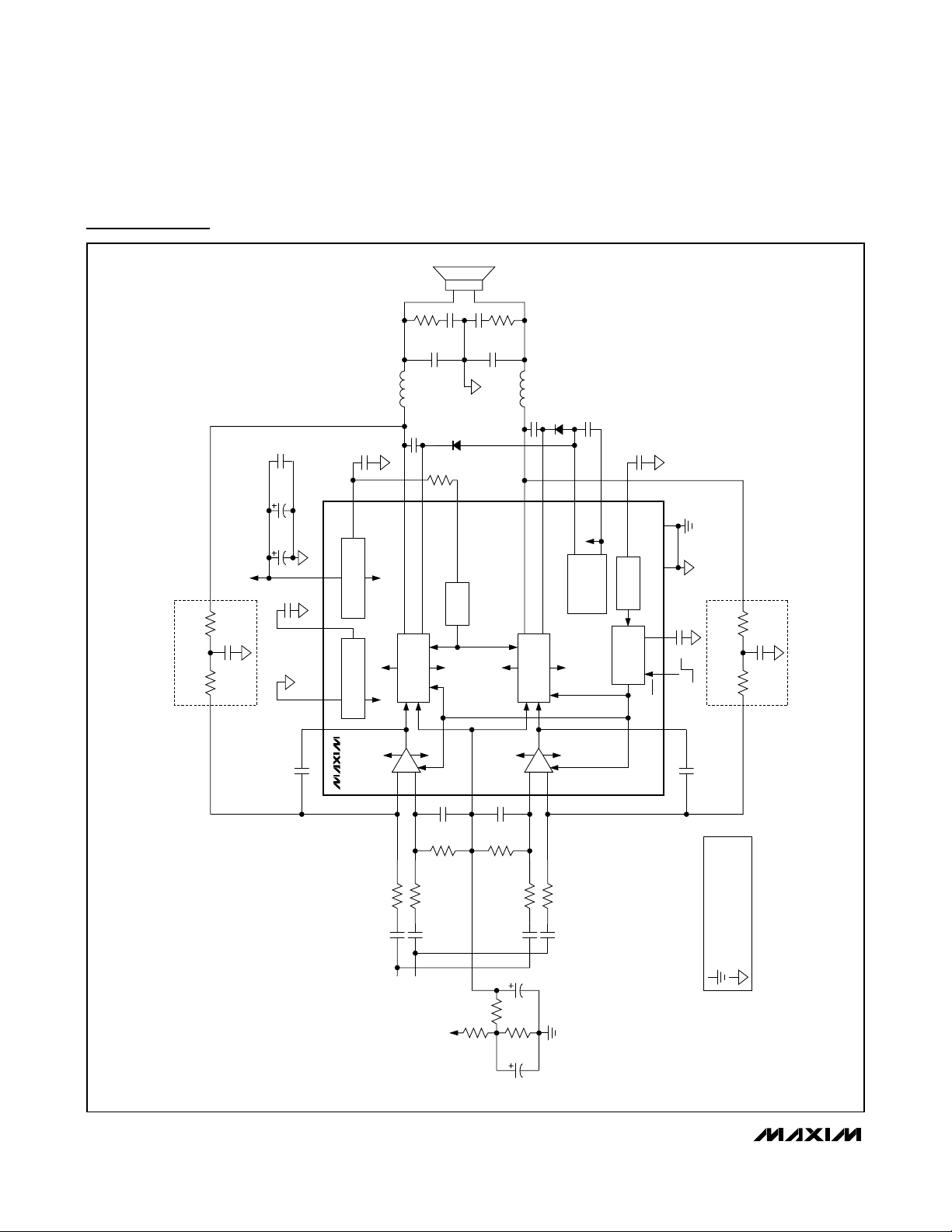
MAX9742
Single-/Dual-Supply, Stereo 16W,
Class D Amplifier with Differential Inputs
34 ______________________________________________________________________________________
Typical Application Circuits/Functional Diagrams (continued)
8Ω
F1b
R
OPTIONAL
F1a
R
ZBL
5Ω
ZBL
R
C
F
C
F
L
DD
29, 30, 34, 35
V
1012REGM
SS
31, 32, 33
V
9
FBL
REGP
C
1µF
REGP
)
MID
+ 5V
V
5V REGULATOR
(WITH RESPECT TO V
)
MID
DD
V
- 5V
-5V REGULATOR
V
(WITH RESPECT TO V
+ 5V
MID
V
MAX9742
MID
MID
INL8
0.1µF
CVDD330µF
DD
330µF
CV
20V TO 40V
REGM
C
1µF
562kΩ
FBL2
10pF
C
121kΩ
FBL1
C
150pF
22µH
2, 3
OUTL
-
CLASS D
INL+
7
0.68µF
BOOT
C
0.1µF
REF
68kΩ
R
5
BOOTL
HALF-BRIDGE
MODULATOR AND
- 5V
MID
V
+
V
0.82µF
BOOT
D
1N4148
13
REFCUR
CURRENT
REFERENCE
SS
11 MID
ZBL
5Ω
ZBL
R
C
0.82µF
F
C
F
0.68µF
L
22µH
DD
V
+ 5V
V
25, 26
OUTR
CLASS D
MID
INR+
21
BOOT
C
24
BOOTR
MODULATOR AND
+
BOOT
0.1µF
D
1N4148
HALF-BRIDGE
- 5V
V
-
INR-
20
REGLS
C
23
REGLS
SS
V
7V REGULATOR
SS
V
MID
1µF
16
22
LV
NSENSE
)
SS
TO V
(WITH RESPECT
CONTROL LOGIC/
LVDD
C
DD
5V SUPPLY
POWER-UP
SEQUENCING
0.1µF
SFT LGND SUB
SHDN
FBR
SFT
C
14 15 4
ON
17
19
F1b
0.47µF
R
562kΩ
OPTIONAL
FBR2
10pF
OFF
FBR1
C
150pF
C
F1a
R
121kΩ
= 44V/V.
V
BRIDGE-TIED-LOAD (BTL), SINGLE-SUPPLY OPERATION
DEVICE CONNECTED FOR A
FBL1
C
150pF
F2
R
681kΩ
IN1
R
IN
C
30.1kΩ
0.47µF
POSITIVE
AUDIO INPUT
IN2
R
C
NEGATIVE
AUDIO INPUT
30.1kΩ
IN
0.47µF
DD
V
FBR1
C
150pF
F2
R
681kΩ
IN2
R
IN
C
R3
10kΩ
R2
R1
10kΩ
IN1
R
30.1kΩ
0.47µF
MID2
C
MID1
C
30.1kΩ
IN
C
0.47µF
10µF
10kΩ
10µF
CONNECT PGND AND SGND TO
= SGND
NEAR THE MAX9742
A SINGLE POINT ON THE PCB
= PGND

MAX9742
Single-/Dual-Supply, Stereo 16W,
Class D Amplifier with Differential Inputs
______________________________________________________________________________________ 35
Package Information
(The package drawing(s) in this data sheet may not reflect the most current specifications. For the latest package outline information,
go to www.maxim-ic.com/packages
.)
QFN THIN.EPS

Package Information (continued)
(The package drawing(s) in this data sheet may not reflect the most current specifications. For the latest package outline information,
go to www.maxim-ic.com/packages
.)
Maxim cannot assume responsibility for use of any circuitry other than circuitry entirely embodied in a Maxim product. No circuit patent licenses are
implied. Maxim reserves the right to change the circuitry and specifications without notice at any time.
36
____________________Maxim Integrated Products, 120 San Gabriel Drive, Sunnyvale, CA 94086 408-737-7600
© 2007 Maxim Integrated Products is a registered trademark of Maxim Integrated Products, Inc.
Single-/Dual-Supply, Stereo 16W,
Class D Amplifier with Differential Inputs
MAX9742
 Loading...