

General Description
The MAX9741 stereo Class D audio power amplifier
provides Class AB amplifier performance with Class D
efficiency, conserving board space and eliminating the
need for a bulky heatsink. Using a high-efficiency Class
D architecture, it delivers 12W continuous output power
into 8Ω loads. Proprietary modulation and switching
schemes render the traditional Class D EMI suppression
output filter unnecessary.
The MAX9741 offers two modulation schemes: a fixed-frequency mode (FFM), and a spread-spectrum mode (SSM)
that reduces EMI-radiated emissions. The device utilizes a
fully differential architecture, a full bridged output, and
offers comprehensive click-and-pop suppression.
The MAX9741 features high 80dB PSRR, low 0.1%
THD+N, and SNR in excess of 100dB. Short-circuit and
thermal-overload protection prevent the device from
being damaged during a fault condition. The MAX9741
is available in a 56-pin TQFN (8mm x 8mm x 0.8mm)
package. The MAX9741 is specified over the extended
-40°C to +85°C temperature range.
Applications
Features
♦ Low-EMI Class D Amplifier
♦ Spread-Spectrum Mode Reduces EMI
♦ Passes FCC EMI Limits with Ferrite Bead Filters
with 0.5m Cables
♦ 12W+12W Continuous Output Power into 8Ω
♦ Low 0.1% THD+N
♦ High PSRR (80dB at 1kHz)
♦ 10V to 25V Single-Supply Operation
♦ Differential Inputs Minimize Common-Mode Noise
♦ Pin-Selectable Gain Reduces Component Count
♦ Industry-Leading Click-and-Pop Suppression
♦ Short-Circuit and Thermal-Overload Protection
♦ Available in Thermally Efficient, Space-Saving
56-Pin TQFN (8mm x 8mm x 0.8mm) Package
MAX9741
12W+12W, Low-EMI, Spread-Spectrum,
Stereo, Class D Amplifier
________________________________________________________________ Maxim Integrated Products 1
19-3887; Rev 0; 2/06
For pricing, delivery, and ordering information, please contact Maxim/Dallas Direct! at
1-888-629-4642, or visit Maxim’s website at www.maxim-ic.com.
EVALUATION KIT
AVAILABLE
Ordering Information
PART
PKG
CODE
MAX9741ETN+
56 TQFN-EP*
T5688-3
+Denotes lead-free package.
*EP = Exposed paddle.
LCD/PDP TVs
CRT TVs
PC Speakers
Pin Configuration appears at end of data sheet.
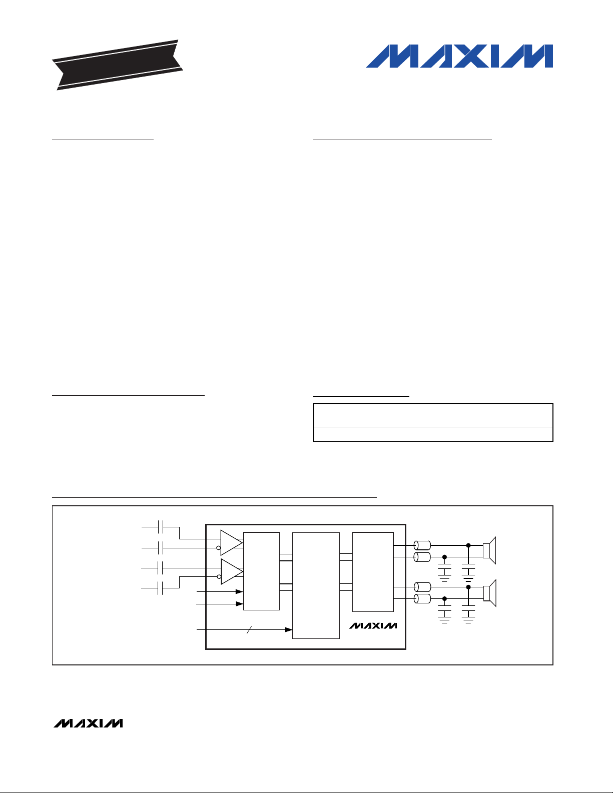
CLASS D
AMPLIFIERS
DRIVE 2 X 12W
INTO 8Ω LOADS
GAIN
CONTROL
INR+
DIFFERENTIAL AUDIO
INPUTS ELIMINATE
NOISE PICKUP
PROGRAMMABLE
SWITCHING
FREQUENCY
INR-
INL+
INL-
FS1, FS2
G2
G1
2
CLASS D
MODULATOR
OUTPUT
PROTECTION
MAX9741
Simplified Block Diagram
TEMP RANGE PIN-PACKAGE
-40°C to +85°C
MAX9741
12W+12W, Low-EMI, Spread-Spectrum,
Stereo, Class D Amplifier
2 _______________________________________________________________________________________
ABSOLUTE MAXIMUM RATINGS
Stresses beyond those listed under “Absolute Maximum Ratings” may cause permanent damage to the device. These are stress ratings only, and functional
operation of the device at these or any other conditions beyond those indicated in the operational sections of the specifications is not implied. Exposure to
absolute maximum rating conditions for extended periods may affect device reliability.
(All voltages referenced to GND.)
V
DD
to PGND, AGND .............................................................30V
OUTR_, OUTL_, C1N..................................-0.3V to (V
DD
+ 0.3V)
C1P............................................(V
DD
- 0.3V) to (CHOLD + 0.3V)
CHOLD........................................................(V
DD
- 0.3V) to +40V
SHDN, FS_, G_ ...........................................................-6.3V to 8V
All Other Pins to GND.............................................-0.3V to +12V
Duration of OUTR_/OUTL_
Short Circuit to GND, V
DD
......................................Continuous
Continuous Input Current (V
DD
, PGND) ..................................2A
Continuous Input Current (all other pins)..........................±20mA
Thermal Limits (Note 1)
Continuous Power Dissipation (T
A
= +70°C)
Single-Layer PC Board
56-Pin TQFN (derate 28.6mW/°C above +70°C) ............2.29W
θ
JA
................................................................................ 35°C/W
θ
JC
............................................................................... 0.6°C/W
Continuous Power Dissipation (T
A
= +70°C)
Multiple-Layer PC Board
56-Pin TQFN (derate 47.6mW/°C above +70°C) ............3.81W
θ
JA
................................................................................ 21°C/W
θ
JC
............................................................................... 0.6°C/W
Junction Temperature......................................................+150°C
Operating Temperature Range ...........................-40°C to +85°C
Storage Temperature Range .............................-65°C to +150°C
Lead Temperature (soldering, 10s) .................................+300°C
ELECTRICAL CHARACTERISTICS
(VDD= 18V, GND = PGND = 0V, SHDN ≥ VIH, AV= 16dB, CSS= CIN= 0.47µF, C
REG
= 0.01µF, C1 = 100nF, C2 = 1µF, FS1 = FS2 =
GND (f
S
= 670kHz), RLconnected between OUTL+ and OUTL- and OUTR+ and OUTR-, TA= T
MIN
to T
MAX
, unless otherwise noted.
Typical values are at T
A
= +25°C.) (Notes 1, 2)
PARAMETER
CONDITIONS
GENERAL
Supply Voltage Range V
DD
Inferred from PSRR test 10 25 V
Quiescent Current I
DD
RL = Open 26 37
Shutdown Current
0.2 1.5 µA
CSS = 470nF 100
Turn-On Time t
ON
CSS = 180nF 50
Amplifier Output Resistance in
Shutdown
SHDN = GND 150 320 kΩ
AV = 13dB 35 53 80
AV = 16dB 30 45 65
AV = 19.1dB 23 36 55
Input Impedance R
IN
AV = 29.6dB 10
22
kΩ
G1 = L, G2 = L
G1 = L, G2 = H
G1 = H, G2 = L
13
Voltage Gain A
V
G1 = H, G2 = H
16
dB
Gain Matching Between channels 0.5 %
Output Offset Voltage V
OS
±5 ±30
Common-Mode Rejection Ratio
fIN = 1kHz, input referred 60 dB
VDD = 10V to 25V 48 83
f
RIPPLE
= 1kHz 80
Power-Supply Rejection Ratio
(Note 3)
PSRR
200mV
P-P
ripple
f
RIPPLE
= 20kHz 60
dB
Note 1: Thermal performance of this device is highly dependant on PC board layout. See the Applications Information for more
detail.
SYMBOL
MIN TYP MAX UNITS
I
SHDN
CMRR
14.3
29.4 29.6 29.8
18.9 19.1 19.3
12.8
15.9
mA
ms
13.2
16.3
mV
MAX9741
12W+12W, Low-EMI, Spread-Spectrum,
Stereo, Class D Amplifier
_______________________________________________________________________________________ 3
ELECTRICAL CHARACTERISTICS (continued)
(VDD= 18V, GND = PGND = 0V, SHDN ≥ VIH, AV= 16dB, CSS= CIN= 0.47µF, C
REG
= 0.01µF, C1 = 100nF, C2 = 1µF, FS1 = FS2 =
GND (f
S
= 670kHz), RLconnected between OUTL+ and OUTL- and OUTR+ and OUTR-, TA= T
MIN
to T
MAX
, unless otherwise noted.
Typical values are at T
A
= +25°C.) (Notes 1, 2)
PARAMETER
CONDITIONS
UNITS
RL = 8Ω 12
VDD = 18V, THD+N =
10%, f = 1kHz
R
L
= 4Ω 6.5
RL = 8Ω 11
VDD = 24V, THD+N =
10%, f = 1kHz
R
L
= 4Ω 5
RL = 8Ω 8
Continuous Output Power
(Notes 4, 5)
VDD = 12V, THD+N =
10%, f = 1kHz
R
L
= 4Ω 8.5
W
Total Harmonic Distortion Plus
Noise
fIN = 1kHz, either FFM or SSM, RL = 8Ω,
P
OUT
= 4W
0.1 %
FFM
SSM
FFM
Signal-to-Noise Ratio SNR
R
L
= 8Ω,
P
OUT
= 4W,
f = 1kHz
SSM
dB
Crosstalk Left to right, right to left, 8Ω load, fIN = 10kHz 65 dB
FS1 = L, FS2 = L 560 670 800
FS1 = L, FS2 = H 930
FS1 = H, FS2 = L 470
Oscillator Frequency f
OSC
FS1 = H, FS2 = H (spread-spectrum mode)
670
kHz
VDD = 12V, RL = 8Ω, P
OUT
= 8W 78
Efficiency (Note 4) η
V
DD
= 18V, RL = 8Ω, P
OUT
= 10W 78
%
Regulator Output V
REG
6V
DIGITAL INPUTS (SHDN, FS_, G_)
V
IH
2.5
Input Thresholds
V
IL
0.8
V
Input Leakage Current ±1µA
Note 2: All devices are 100% production tested at +25°C. All temperature limits are guaranteed by design.
Note 3: PSRR is specified with the amplifier inputs connected to GND through C
IN
.
Note 4: Testing performed with a resistive load in series with an inductor to simulate an actual speaker load. For R
L
= 8Ω, L = 68µH.
For R
L
= 12Ω, L = 100µH. For RL= 16Ω, L = 120µH.
Note 5: Output power measured at T
A
= +25°C, with a soak time of 15 minutes.
SYMBOL
P
THD+N
CONT
BW = 22Hz to 22kHz
Unweighted
A-weighted
MIN TYP MAX
95.8
91.8
99.1
95.7
±7%
MAX9741
12W+12W, Low-EMI, Spread-Spectrum,
Stereo, Class D Amplifier
4 _______________________________________________________________________________________
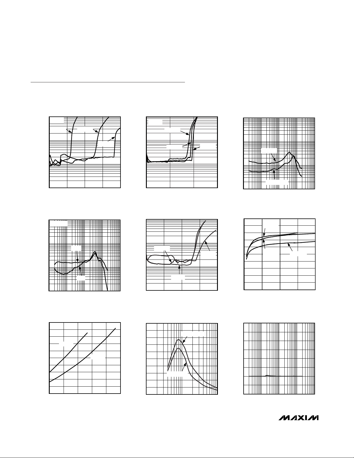
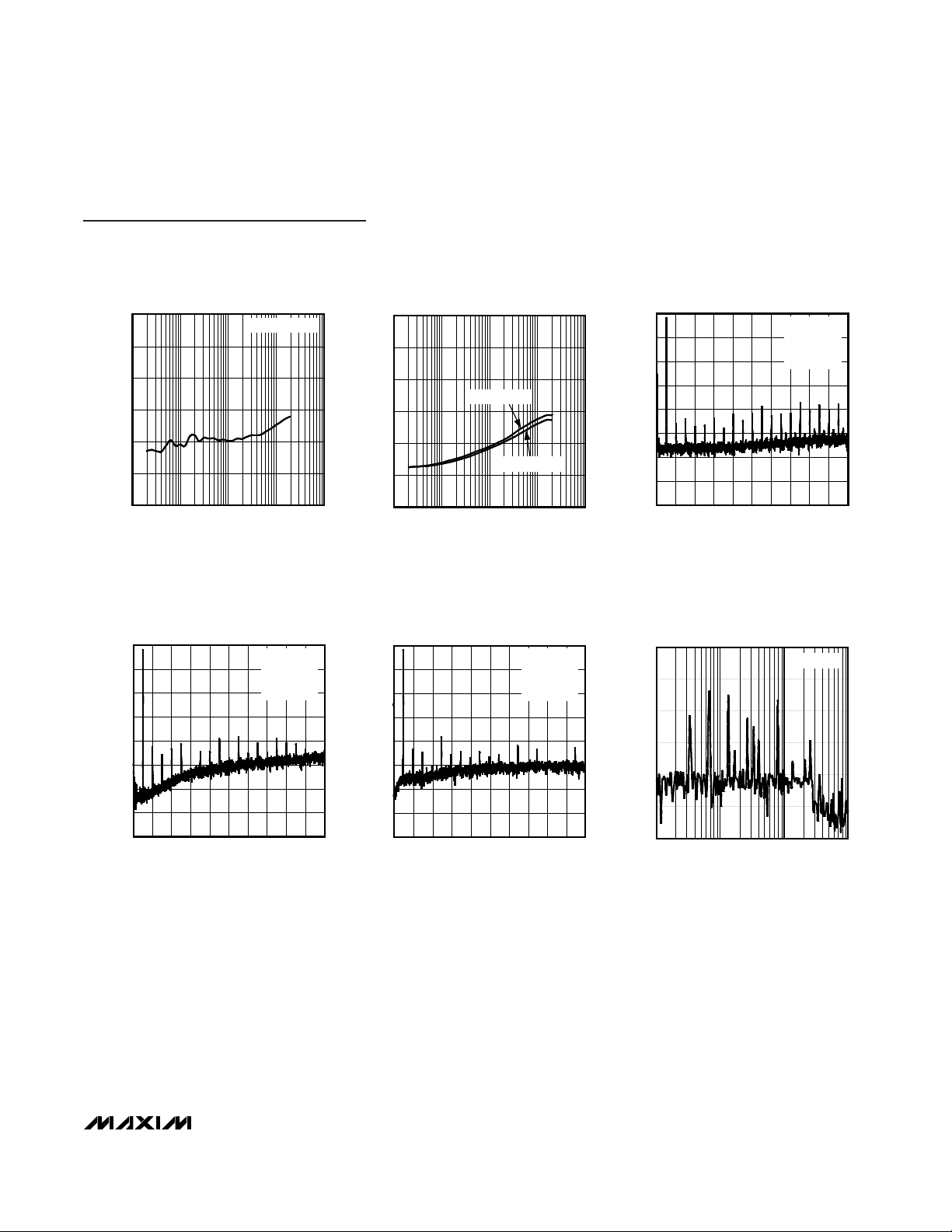
TOTAL HARMONIC DISTORTION PLUS
NOISE vs. OUTPUT POWER
MAX9741 toc01
OUTPUT POWER (W)
THD+N (%)
15105
0.1
1
10
0.01
020
RL = 8Ω
VDD = 24V
VDD = 18V
VDD = 12V
15
TOTAL HARMONIC DISTORTION PLUS
NOISE vs. OUTPUT POWER
MAX9741 toc02
OUTPUT POWER (W)
THD+N (%)
0.01
0.1
1
10
0
RL = 4Ω
VDD = 24V
VDD = 18V
VDD = 12V
105
TOTAL HARMONIC DISTORTION PLUS
NOISE vs. FREQUENCY
MAX9741 toc03
FREQUENCY (Hz)
THD+N (%)
10k1k100
0.1
1
10
0.01
10 100k
P
OUT
= 500mW
P
OUT
= 8W
TOTAL HARMONIC DISTORTION PLUS
NOISE vs. FREQUENCY
MAX974 toc04
FREQUENCY (Hz)
THD+N (%)
10k1k100
0.1
1
10
0.01
10 100k
P
OUT
= 8W
SSM
FFM
OUTPUT POWER vs. SUPPLY VOLTAGE
MAX9741 toc07
SUPPLY VOLTAGE (V)
OUTPUT POWER (W)
0
6
4
2
8
10
12
14
16
18
20
10 1613 19 22 25
RL = 8Ω
RL = 16Ω
TOTAL HARMONIC DISTORTION PLUS
NOISE vs. OUTPUT POWER
MAX9741 toc05
OUTPUT POWER (W)
THD+N (%)
15105
0.1
1
10
0.01
020
f = 100Hz
f = 10kHz
f = 1kHz
EFFICIENCY vs. OUTPUT POWER
MAX9741 toc06
OUTPUT POWER (W)
EFFICIENCY (%)
161248
10
20
30
40
50
60
70
80
90
100
0
0
RL = 8Ω
VDD = 18V
VDD = 12V
VDD = 24V
OUTPUT POWER vs. LOAD RESISTANCE
MAX9741 toc08
LOAD RESISTANCE (Ω)
OUTPUT POWER (W)
10
2
4
6
8
10
12
14
16
18
20
0
1 100
THD+N = 10%
THD+N = 1%
COMMON-MODE REJECTION RATIO
vs. FREQUENCY
MAX9741 toc09
FREQUENCY (Hz)
CMRR (dB)
10k1k100
-70
-60
-50
-40
-30
-20
-10
0
-80
10 100k
Typical Operating Characteristics
(VDD= 18V, RL= 8Ω, fIN= 1kHz, 33µH with 4Ω, 68µH with 8Ω, part in SSM mode, 136µH with 16Ω, measurement BW = 22Hz to
22kHz, unless otherwise noted.)
MAX9741
12W+12W, Low-EMI, Spread-Spectrum,
Stereo, Class D Amplifier
_______________________________________________________________________________________ 5
POWER-SUPPLY REJECTION RATIO
vs. FREQUENCY
MAX9741 toc10
FREQUENCY (Hz)
PSRR (dB)
10k1k100
-100
-80
-60
-40
-20
0
-120
10 100k
200mV
P-P
INPUT
CROSSTALK vs. FREQUENCY
MAX9741 toc11
FREQUENCY (Hz)
CROSSTALK (dB)
10k1k100
-80
-100
-60
-40
-20
0
-120
10 100k
LEFT TO RIGHT
RIGHT TO LEFT
OUTPUT FREQUENCY SPECTRUM
MAX9741 toc12
FREQUENCY (kHz)
OUTPUT MAGNITUDE (dB)
-120
-100
-80
-60
-40
-20
0
20
-140
181612 144 6 8 102020
FFM MODE
UNWEIGHTED
f
IN
= 1kHz
P
OUT
= 5W
OUTPUT FREQUENCY SPECTRUM
MAX941 toc13
FREQUENCY (kHz)
OUTPUT MAGNITUDE (dB)
-120
-100
-80
-60
-40
-20
0
20
-140
181612 144 6 8 102020
SSM MODE
UNWEIGHTED
f
IN
= 1kHz
P
OUT
= 5W
OUTPUT FREQUENCY SPECTRUM
MAX9741 toc14
FREQUENCY (kHz)
OUTPUT MAGNITUDE (dB)
-120
-100
-80
-60
-40
-20
0
20
-140
181612 144 6 8 102020
SSM MODE
A-WEIGHTED
f
IN
= 1kHz
P
OUT
= 5W
100k 1M 10M 100M
WIDEBAND OUTPUT SPECTRUM
(FFM MODE)
MAX9741 toc15
FREQUENCY (Hz)
OUTPUT AMPLITUDE (dBV)
0
-120
-100
-80
-60
-40
-20
RBW = 10kHz
Typical Operating Characteristics (continued)
(VDD= 18V, RL= 8Ω, fIN= 1kHz, 33µH with 4Ω, 68µH with 8Ω, part in SSM mode, 136µH with 16Ω, measurement BW = 22Hz to
22kHz, unless otherwise noted.)

MAX9741
12W+12W, Low-EMI, Spread-Spectrum,
Stereo, Class D Amplifier
6 _______________________________________________________________________________________
15
TOTAL HARMONIC DISTORTION PLUS
NOISE vs. OUTPUT POWER
WITH FERRITE BEAD FILTER
MAX9741 toc19
OUTPUT POWER (W)
THD+N (%)
0.01
0.1
1
10
0
RL = 4Ω
105
VDD = 18V
VDD = 12V
VDD = 24V
SUPPLY CURRENT
vs. SUPPLY VOLTAGE
MAX9741 toc20
SUPPLY VOLTAGE (V)
SUPPLY CURRENT (mA)
22191613
10
5
15
20
25
30
35
0
10 25
SHUTDOWN SUPPLY CURRENT
vs. SUPPLY VOLTAGE
MAX9741 toc21
SUPPLY VOLTAGE (V)
SUPPLY CURRENT (µA)
18161412
0.10
0.05
0.15
0.20
0.25
0.30
0.35
0
10 20
Typical Operating Characteristics (continued)
(VDD= 18V, RL= 8Ω, fIN= 1kHz, 33µH with 4Ω, 68µH with 8Ω, part in SSM mode, 136µH with 16Ω, measurement BW = 22Hz to
22kHz, unless otherwise noted.)
100k 1M 10M 100M
WIDEBAND OUTPUT SPECTRUM
(SSM MODE)
MAX9741 toc16
FREQUENCY (Hz)
OUTPUT AMPLITUDE (dBV)
0
-120
-100
-80
-60
-40
-20
RBW = 10kHz
TURN-ON/TURN-OFF RESPONSE
MAX9741 toc17
20ms/div
OUTPUT
1V/div
SHDN
5V/div
f = 1kHz
CSS = 180pF
TOTAL HARMONIC DISTORTION
PLUS NOISE vs. OUTPUT POWER
WITH FERRITE BEAD FILTER
MAX9741 toc18
OUTPUT POWER (W)
THD+N (%)
15105
0.1
1
10
0.01
020
RL = 8Ω
VDD = 18V
VDD = 12V
VDD = 24V

MAX9741
12W+12W, Low-EMI, Spread-Spectrum,
Stereo, Class D Amplifier
_______________________________________________________________________________________ 7
Detailed Description
The MAX9741 low-EMI, Class D audio power amplifier
features several improvements to switch-mode amplifier technology. This device offers Class AB performance with Class D efficiency, while occupying
minimal board space. A unique modulation scheme
and spread-spectrum switching mode create a compact, flexible, low-noise, efficient audio power amplifier.
The differential input architecture reduces commonmode noise pickup, and can be used without inputcoupling capacitors. The device can also be
configured as a single-ended input amplifier.
PIN NAME FUNCTION
1, 4, 7, 11–15, 19, 21,
23, 25, 28, 33–36, 39,
42, 43, 44, 49, 50, 55, 56
N.C. No Connection. Not internally connected.
2, 3, 40, 41 PGND Power Ground
5, 6, 37, 38 V
DD
Power-Supply Input
8 C1N Charge-Pump Flying Capacitor Negative Terminal
9 C1P Charge-Pump Flying Capacitor Positive Terminal
10
Charge-Pump Hold Capacitor. Connect a 1µF capacitor from CHOLD to VDD.
16 INL- Left-Channel Negative Input
17 INL+ Left-Channel Positive Input
18 SHDN
Active-Low Shutdown. Connect SHDN to GND to disable the device. Connect to V
DD
for
normal operation.
20 SS Soft-Start. Connect a 0.47µF capacitor from SS to GND to enable soft-start feature.
22 AGND Analog Ground
24 REG Internal Regulator Output. Bypass with a 0.01µF capacitor to PGND.
26 INR- Right-Channel Negative Input
27 INR+ Right-Channel Positive Input
29 G1 Gain-Select Input 1
30 G2 Gain-Select Input 2
31 FS1 Frequency-Select Input 1
32 FS2 Frequency-Select Input 2
45, 46 OUTR- Right-Channel Negative Audio Output
47, 48
Right-Channel Positive Audio Output
51, 52 OUTL- Left-Channel Negative Audio Output
53, 54
Left-Channel Positive Audio Output
—EPExposed Paddle. Connect to GND.
Pin Description
CHOLD
OUTR+
OUTL+

Operating Modes
Fixed-Frequency Modulation (FFM) Mode
The MAX9741 features three FFM modes with different
switching frequencies (Table 1). In FFM mode, the frequency spectrum of the Class D output consists of the
fundamental switching frequency and its associated
harmonics (see the Wideband Output Spectrum graph
in the Typical Operating Characteristics). The MAX9741
allows the switching frequency to be changed by
±35%, should the frequency of one or more of the harmonics fall in a sensitive band. This can be done at any
time and does not affect audio reproduction.
Spread-Spectrum Modulation (SSM) Mode
A unique, proprietary spread-spectrum mode flattens
the wideband spectral components, improving EMI
emissions that may be radiated by the speaker and
cables. This mode is enabled by setting FS1 = FS2 =
H. In SSM mode, the switching frequency varies randomly by ±7% around the center frequency (670kHz).
The modulation scheme remains the same, but the
period of the triangle waveform changes from cycle to
cycle. Instead of a large amount of spectral energy present at multiples of the switching frequency, the energy
is now spread over a bandwidth that increases with frequency. Above a few megahertz, the wideband spectrum looks like white noise for EMI purposes.
Efficiency
Efficiency of a Class D amplifier is attributed to the region
of operation of the output stage transistors. In a Class D
amplifier, the output transistors act as current-steering
switches and consume negligible additional power.
The theoretical best efficiency of a linear amplifier is
78%; however, that efficiency is only exhibited at peak
output powers. Under normal operating levels (typical
music reproduction levels), efficiency falls below 30%,
whereas the MAX9741 still exhibits > 78% efficiency
under the same conditions (Figure 1).
Shutdown
A shutdown mode reduces power consumption and
extends battery life. Driving SHDN low places the
device in low-power (0.2µA) shutdown mode. Connect
SHDN to a logic-high for normal operation.
Click-and-Pop Suppression
Comprehensive click-and-pop suppression eliminates
audible transients on startup and shutdown. While in
shutdown, the H-bridge is pulled to GND through 320kΩ.
During startup, or power-up, the input amplifiers are
muted and an internal loop sets the modulator bias voltages to the correct levels, preventing clicks and pops
when the H-bridge is subsequently enabled. Following
startup, a soft-start function gradually unmutes the input
amplifiers. The value of the soft-start capacitor has an
impact on the click/pop levels. For optimum performance,
C
SS
should be 470nF with a voltage rating of at least 7V.
Mute Function
The MAX9741 features a clickless/popless mute mode.
When the device is muted, the outputs stop switching,
muting the speaker. Mute only affects the output stage
and does not shut down the device. To mute the
MAX9741, drive SS to GND by using a MOSFET pulldown (Figure 2). Driving SS to GND during the powerup/down or shutdown/turn-on cycle optimizes
click-and-pop suppression.
MAX9741
12W+12W, Low-EMI, Spread-Spectrum,
Stereo, Class D Amplifier
8 _______________________________________________________________________________________
MAX9741
SS
0.47µF
GPIO
MUTE SIGNAL
Figure 2. MAX9741 Mute Circuit
Table 1. Operating Modes
FS1 FS2
SWITCHING MODE
(kHz)
LL 670
LH 930
HL 470
HH670 ±7%
Figure 1. MAX9741 Efficiency vs. Class AB Efficiency
0
30
20
10
40
50
60
70
80
90
100
0
6
8
10 12 141618
24
20
EFFICIENCY vs. OUTPUT POWER
OUTPUT POWER (W)
EFFICIENCY (%)
VDD = 15V
f = 1kHz
R
L
= 8Ω
MAX9741
CLASS AB

MAX9741
12W+12W, Low-EMI, Spread-Spectrum,
Stereo, Class D Amplifier
_______________________________________________________________________________________ 9
Internal Regulator
The MAX9741 has an internal linear regulator, REG,
used to power the internal analog circuitry. The voltage
at REG is nominally 6V. Bypass REG to AGND with a
10nF capacitor, rated for at least 10V. REG is turned off
in shutdown.
Applications Information
Class D Amplifier Outputs
Class D amplifiers differ from analog amplifiers such as
Class AB in that their output waveform is composed of
high-frequency pulses from ground to the supply rail.
When viewed with an oscilloscope the audio signal will
not be seen; instead, the high-frequency pulses dominate. To evaluate the output of a Class D amplifier
requires taking the difference from the positive and
negative outputs, then lowpass filtering the difference
to recover the amplified audio signal.
Ferrite Bead Output Filters
The MAX9741’s low-EMI output switching method
reduces the output filtering requirements when compared
to pure PWM Class D amplifiers. The outputs will contain
both differential and common-mode noise at the switching frequency and its harmonics. In many applications,
a simple ferrite bead filter (see the Simplified Block
Diagram) will allow the amplifier to pass FCC EMI limits.
Ferrite beads offer significant cost and size reductions
when compared to conventional inductors. The ferrite
bead type and capacitor value can be adjusted to tune
the rejection to match the speaker cable length.
Actual EMI test results for the MAX9741 are shown in
Figure 3. This shows the MAX9741, tested in a 10m anechoic EMC chamber. The MAX9741 test conditions
were: SSM mode, 0.5m cables on each side, 16dB gain,
18V supply voltage, both channels playing pink noise at
4W per channel into 8Ω shielded speakers.
The graph of Figure 3 indicates peak readings. Actual
quasi peak readings per EN55022B specification will
be lower due to Maxim’s proprietary SSM mode. Table
2 lists select values, indicating the peak reading, the
quasi-peak reading, and the actual margin to
EN55022B specification.
FREQUENCY (MHz)
AMPLITUDE (dBuV/m)
900800100 200 300 500 600400 700
10
15
20
25
30
35
40
30 1000
Figure 3. EMI Measurement of MAX9741 in 10m Anechoic Chamber
Table 2. Peak and Quasi-Peak EMI Readings
FREQUENCY
(MHz)
PRELIMINARY PEAK
READING (dBµV/m)
QUASI PEAK READING
(dBµV/m)
EN55022B LIMIT
(dBµV/m)
ACTUAL MARGIN
(dBµV/m)
75.38 28.1 18.3 30.0 11.7
78.57 28.0 21.9 30.0 -8.1
83.18 26.6 20.6 30.0 -9.4

MAX9741
12W+12W, Low-EMI, Spread-Spectrum,
Stereo, Class D Amplifier
10 ______________________________________________________________________________________
Ferrite beads are available from many manufacturers.
Table 3 lists some manufacturers who make ferrite
beads and other products suitable for use with Class D
amplifiers.
Although they offer a low cost and small size, ferrite
bead filters slightly increase distortion and slightly
reduce efficiency. If the audio performance of the ferrite
bead filters does not meet the system requirements, then
a full inductor/capacitor (LC) filter should be considered.
Inductor/Capacitor Output Filters
Using a full inductor and capacitor (LC) output filter
provides significant attenuation of the fundamental
switching energy.
Select inductors rated for the expected RMS current
load. For example, if using a Class D amplifier up to
10W into 8Ω, the inductor should be rated for 1.25A
RMS or more. Furthermore, the inductor should maintain
a constant inductance value across the expected current range. Inductors which change in value as a function of current will cause harmonic distortion.
The output capacitors can also affect audio performance. Ceramic capacitors are often selected for their
size and cost advantage, but they cause distortion. If
the application constraints dictate ceramic capacitors,
selecting higher voltage rating and larger package size
mitigates some of the shortcomings. Best performance
is obtained with plastic film capacitors, but these are
larger and more expensive.
Filterless Operation
In some cases, a Class D amplifier can be used without
an output filter. The intrinsic inductance of the loudspeaker stores energy from the high-speed PWM pulses,
converting these into power in the audible frequency
range. Filterless operation requires the Class D amplifier to be very close to the speaker. Distances greater
than a few centimeters must be evaluated for EMC
compliance.
Gain Selection
Table 4 shows the suggested gain settings to attain a
maximum output power from a given peak input voltage
and given load.
Output Offset
Unlike a Class AB amplifier, the output offset voltage of
Class D amplifiers does not noticeably increase quiescent current draw when a load is applied. This is due to
the power conversion of the Class D amplifier. For
example, an 8mVDC offset across an 8Ω load results in
1mA extra current consumption in a Class AB device.
In the Class D case, an 8mV offset into 8Ω equates
to an additional power drain of 8µW. Due to the high
efficiency of the Class D amplifier, this represents an
additional quiescent current draw of: 8µW / (V
DD
/ 100 ✕
η), which is in the order of a few microamps.
Input Amplifier
Differential Input
The MAX9741 features a differential input structure, making them compatible with many CODECs, and offering
improved noise immunity over a single-ended input amplifier. In devices such as PCs, noisy digital signals can be
picked up by the amplifier’s input traces. The signals
appear at the amplifiers’ inputs as common-mode noise. A
differential input amplifier amplifies the difference of the
two inputs, any signal common to both inputs is canceled.
Table 4. Gain Settings
G1 G2 GAIN (dB)
0029.6
0119.1
1013
1116
Table 3. Filter Component Suppliers
SUPPLIER
PRODUCT WEBSITE
Murata
Ferrite beads,
capacitors
www.murata.com
Taiyo Yuden
Ferrite beads,
capacitors
www.t-yuden.com
TDK
Ferrite beads,
capacitors
www.tdk.co.jp/tetop01
Fairrite Ferrite beads www.fair-rite.com
Coilcraft Inductors www.coilcraft.com
Sumida Inductors www.sumida.com
Panasonic Inductors
www.panasonic.com/indu
strial/components

MAX9741
12W+12W, Low-EMI, Spread-Spectrum,
Stereo, Class D Amplifier
______________________________________________________________________________________ 11
Single-Ended Input
The MAX9741 can be configured as single-ended input
amplifiers by capacitively coupling either input to GND
and driving the other input (Figure 4).
Component Selection
Input Filter
An input capacitor, CIN, in conjunction with the input
impedance of the MAX9741, forms a highpass filter that
removes the DC bias from an incoming signal. The ACcoupling capacitor allows the amplifier to bias the signal to an optimum DC level. Assuming zero-source
impedance, the -3dB point of the highpass filter is
given by:
Choose CINso f
-3dB
is well below the lowest frequency
of interest. Setting f
-3dB
too high affects the low-frequency response of the amplifier. Use capacitors with
dielectrics that have low-voltage coefficients, such as
tantalum or aluminum electrolytic. Capacitors with highvoltage coefficients, such as ceramics, may result in
increased distortion at low frequencies.
Charge-Pump Capacitor Selection
Use capacitors with an ESR less than 100mΩ for optimum performance. Low-ESR ceramic capacitors minimize the output resistance of the charge pump. For
best performance over the extended temperature
range, select capacitors with an X7R dielectric.
Flying Capacitor (C1)
The value of the flying capacitor (C1) affects the load
regulation and output resistance of the charge pump. A
C1 value that is too small degrades the device’s ability
to provide sufficient current drive. Increasing the value
of C1 improves load regulation and reduces the
charge-pump output resistance to an extent. Above
1µF, the on-resistance of the switches and the ESR of
C1 and C2 dominate.
Hold Capacitor (C2)
The output capacitor value and ESR directly affect the ripple at CHOLD. Increasing C2 reduces output ripple.
Likewise, decreasing the ESR of C2 reduces both ripple
and output resistance. Lower capacitance values can be
used in systems with low maximum output power levels.
Sharing Input Sources
In certain systems, a single audio source can be shared
by multiple devices (speaker and headphone amplifiers).
When sharing inputs, it is common to mute the unused
device, rather than completely shutting it down, preventing the unused device inputs from distorting the input
signal. Mute the MAX9741 by driving SS low through an
open-drain output or MOSFET. Driving SS low turns off
the Class D output stage, but does not affect the input
bias levels of the MAX9741. Be aware that during normal
operation, the voltage at SS can be up to 7V, depending
on the MAX9741 supply.
Supply Bypassing/Layout
Proper power-supply bypassing ensures low-distortion
operation. For optimum performance, bypass VDDto
PGND with a 0.1µF or greater capacitor as close to each
V
DD
pin as possible. In some applications, a 0.1µF
capacitor in parallel with a larger value, low-ESR ceramic
or aluminum electrolytic capacitor provides good results.
A low-impedance, high-current power-supply connection
to V
DD
is assumed. Additional bulk capacitance should
be added as required depending on the application and
power-supply characteristics. AGND and PGND should
be star connected to system ground. Refer to the
MAX9741 Evaluation Kit for layout guidance.
Class D Amplifier Thermal Considerations
Class D amplifiers provide much better efficiency and
thermal performance than a comparable Class AB
amplifier. However, the system’s thermal performance
must be considered with realistic expectations and
consideration of many parameters. This application
note examines Class D amplifiers using general examples to illustrate good design practices.
Continuous Sine Wave vs. Music
When a Class D amplifier is evaluated in the lab, often
a continuous sine wave is used as the signal source.
While this is convenient for measurement purposes, it
represents a worst-case scenario for thermal loading
on the amplifier. It is not uncommon for a Class D
amplifier to enter thermal shutdown if driven near maximum output power with a continuous sine wave.
f
RC
-3dB
IN IN
1
2=π
MAX9741
IN+
IN-
0.47µF
0.47µF
SINGLE-ENDED
AUDIO INPUT
Figure 4. Single-Ended Input

MAX9741
12W+12W, Low-EMI, Spread-Spectrum,
Stereo, Class D Amplifier
12 ______________________________________________________________________________________
Audio content, both music and voice, has a much lower
RMS value relative to its peak output power. Figure 5
shows a sine wave and an audio signal in the time
domain. Both are measured for RMS value by the oscilloscope. Although the audio signal has a slightly higher
peak value than the sine wave, its RMS value is almost
half that of the sine wave. Therefore, while an audio signal may reach similar peaks as a continuous sine wave,
the actual thermal impact on the Class D amplifier is
highly reduced. If the thermal performance of a system
is being evaluated, it is important to use actual audio
signals instead of sine waves for testing. If sine waves
must be used, the thermal performance will be less
than the system’s actual capability.
PC Board Thermal Considerations
The exposed pad is the primary route of heat away
from the IC. With a bottom-side exposed pad, the PC
board and its copper becomes the primary heatsink for
the Class D amplifier. Solder the exposed pad to a
large copper polygon. Add as much copper as possible from this polygon to any adjacent pin on the Class
D amplifier as well as to any adjacent components, provided these connections are at the same potential.
These copper paths must be as wide as possible. Each
of these paths contributes to the overall thermal capabilities of the system.
The copper polygon to which the exposed pad is
attached should have multiple vias to the opposite side
of the PC board, where they connect to another copper
polygon. Make this polygon as large as possible within
the system’s constraints for signal routing.
Additional improvements are possible if all the traces
from the device are made as wide as possible.
Although the IC pins are not the primary thermal path
out of the package, they do provide a small amount.
The total improvement would not exceed approximately
10%, but it could make the difference between acceptable performance and thermal problems.
With a bottomside exposed pad, the lowest resistance
thermal path is on the bottom of the PC board. The topside
of the IC is not a significant thermal path for the device.
Thermal Calculations
The die temperature of a Class D amplifier can be estimated with some basic calculations. For example, the
die temperature is calculated for the below conditions:
•T
A
= +40°C
•P
OUT
= 10W (5W + 5W)
• Efficiency (η) = 78%
• θJA= 21°C/W
First, the Class D amplifier’s power dissipation must be
calculated.
Then the power dissipation is used to calculate the die
temperature, TC, as follows:
Load Impedance
The on-resistance of the MOSFET output stage in Class
D amplifiers affects both the efficiency and the peakcurrent capability. Reducing the peak current into the
load reduces the I2R losses in the MOSFETs, increasing efficiency. To keep the peak currents lower, choose
the highest impedance speaker which can still deliver
the desired output power within the voltage swing limits
of the Class D amplifier and its supply voltage.
Optimize MAX9741 Efficiency with
Load Impedance and Supply Voltage
To optimize efficiency, load the output stage with 12Ω
to 16Ω speakers. The MAX9741 exhibits highest efficiency performance when driving higher load impedance (see the Typical Operating Characteristics). If a
12Ω to 16Ω load is not available, select a lower supply
voltage when driving 4Ω to 10Ω loads.
For best performance, choose a speaker impedance to
complement the required output power and the available
supply voltage. For example, if operating from a 24V supply and a peak output of 10W per channel is desired, using
12Ω speakers provides the best audio performance and
power efficiency. The amplifier outputs are short-circuit
protected at approximately 2A. Selecting a higher impedance driver helps prevent exceeding the current limit.
TTP C W CW C
CADISS JA
=+ × =°+ ×° = °θ 40 2 82 21 99 2./.
P
P
P
W
WW
DISS
OUT
OUT
===−−
η
10
78
10 2 82%.
20ms/div
Figure 5. RMS Comparison of Sine Wave vs. Audio Signal

MAX9741
12W+12W, Low-EMI, Spread-Spectrum,
Stereo, Class D Amplifier
______________________________________________________________________________________ 13
MAX9741
0.47µF
LOGIC INPUTS SHOWN FOR A
V
= 16dB (SSM).
V
IN
= LOGIC-HIGH > 2.5V.
*CAPACITOR VOLTAGE RATINGS MAY BE REDUCED WHEN
OPERATING WITH REDUCED SUPPLY VOLTAGES.
INL+17
16
31
18
29
30
20
22 AGND
24
9
8
32
INL-
FS1
V
REG
V
REG
V
REG
V
REG
FS2
G1
G2
SS
REG
0.47µF
MODULATOR
OSCILLATOR
CHARGE PUMP
C1P
C1
0.1µF
25V
C1N
0.47µF
V
IH
GAIN
CONTROL
SHUTDOWN
CONTROL
0.01µF
10V
SHDN
H-BRIDGE
OUTL+
OUTL+
OUTL-
OUTL-
54
53
52
51
PGND V
DD
V
DD
PGND
256373840413
10V TO 25V
33µF
25V
2.2µF
25V*
2.2µF
25V*
C2
1µF
25V
CHOLD
V
DD
10
0.47µF
INR+
26
27
INR-
0.47µF
MODULATOR
H-BRIDGE
OUTR+
OUTR+
OUTR-
OUTR-
48
47
46
45
V
REG
Application Circuit

MAX9741
12W+12W, Low-EMI, Spread-Spectrum,
Stereo, Class D Amplifier
14 ______________________________________________________________________________________
TOP VIEW
MAX9741
THIN QFN
8mm x 8mm
15
17
16
18
19
20
21
22
23
24
25
26
27
28
N.C.
INL-
INL+
SHDN
N.C.
SS
N.C.
AGND
N.C.
REG
N.C.
INR-
INR+
N.C.
N.C.
N.C.
OUTL+
OUTL+
OUTL-
OUTL-
N.C.
N.C.
OUTR+
OUTR+
OUTR-
OUTR-
N.C.
N.C.
48
47
46
45
44
43
54
53
56
55
52
51
50
49
1234567891011121314
42 41 40 39 38 37 36 35 34 33 32 31 30 29
N.C.
N.C.
N.C.
N.C.
CHOLD
C1P
C1N
N.C.
V
DDVDD
N.C.
PGND
PGND
N.C.
FS1G2G1
FS2
N.C.
N.C.
N.C.
N.C.
V
DDVDD
N.C.
PGND
PGND
N.C.
+
Pin Configuration
Chip Information
TRANSISTOR COUNT: 4630
PROCESS: BiCMOS

MAX9741
12W+12W, Low-EMI, Spread-Spectrum,
Stereo, Class D Amplifier
______________________________________________________________________________________ 15
56L THIN QFN.EPS
PACKAGE OUTLINE
21-0135
2
1
E
56L THIN QFN, 8x8x0.8mm
Package Information
(The package drawing(s) in this data sheet may not reflect the most current specifications. For the latest package outline information,
go to www.maxim-ic.com/packages
.)

MAX9741
12W+12W, Low-EMI, Spread-Spectrum,
Stereo, Class D Amplifier
Maxim cannot assume responsibility for use of any circuitry other than circuitry entirely embodied in a Maxim product. No circuit patent licenses are
implied. Maxim reserves the right to change the circuitry and specifications without notice at any time.
16 ____________________Maxim Integrated Products, 120 San Gabriel Drive, Sunnyvale, CA 94086 408-737-7600
© 2006 Maxim Integrated Products Printed USA is a registered trademark of Maxim Integrated Products, Inc.
Quijano
PACKAGE OUTLINE
21-0135
2
2
E
56L THIN QFN, 8x8x0.8mm
Package Information (continued)
(The package drawing(s) in this data sheet may not reflect the most current specifications. For the latest package outline information
go to www.maxim-ic.com/packages
.)
 Loading...