

General Description
The MAX971–MAX974 and MAX981–MAX984 single/
dual/quad low-voltage comparators feature the lowest
power consumption available. These micropower
devices draw less than 4µA supply current over
temperature (MAX971/MAX972/MAX981/MAX982), and
include an internal 1.182V ±1% (MAX971/MAX973/
MAX974) or ±2% (MAX981–MAX984) voltage reference
and programmable hysteresis.
Ideal for 3V or 5V single-supply applications, these
devices operate from a single 2.5V to 11V supply (or
±1.25V to ±5.5V dual supplies), and each comparator’s
input voltage ranges from the negative supply rail to within
1.3V of the positive supply.
The single MAX971/MAX981 and the dual MAX973/
MAX982/MAX983 provide a unique, simple method for
adding hysteresis without feedback or complicated
equations, simply by using the HYST pin plus two
resistors.
The MAX971–MAX974 and MAX981–MAX984’s opendrain outputs permit wire-ORed configurations. Thanks to
an 11V output range and separate GND pin for the output
transistor (MAX971/MAX974, MAX981/MAX984), these
devices are ideal for level translators and bipolar to singleended converters. For similar devices with complementary
output stages, see the MAX921–MAX924 (1% reference)
and the MAX931–MAX934 (2% reference).
Features
♦ Available in Ultra-Small Packages:
UCSP™ (MAX972)
µMAX (MAX9_1/MAX9_2/MAX9_3)
♦ Ultra-Low Quiescent Current (4µA, max)
Over Extended Temp Range (MAX971/MAX981)
♦ Power Supplies:
Single 2.5V to 11V
Dual ±1.25V to ±5.5V
♦ Input Voltage Range Includes Negative Supply
♦ Internal Bandgap Reference
1.182V ±1% (MAX97_)
1.182V ±2% (MAX98_)
♦ 12µs Propagation Delay (10mV Overdrive)
♦ Output Has Separate GND Pin (MAX9_1/MAX9_4)
Applications
MAX971–MAX974/MAX981–MAX984
Ultra-Low-Power, Open-Drain,
Single/Dual-Supply Comparators
________________________________________________________________________________________ 1
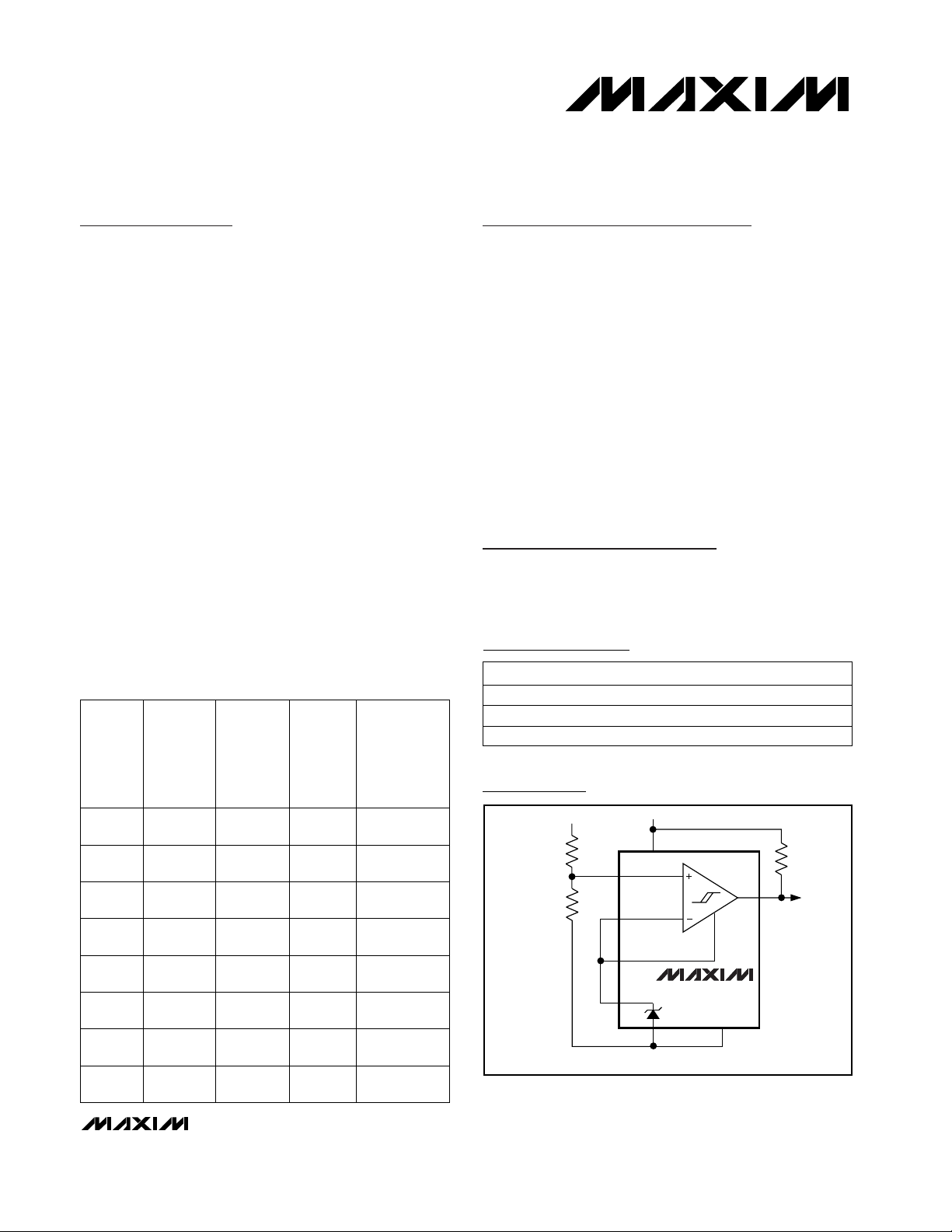
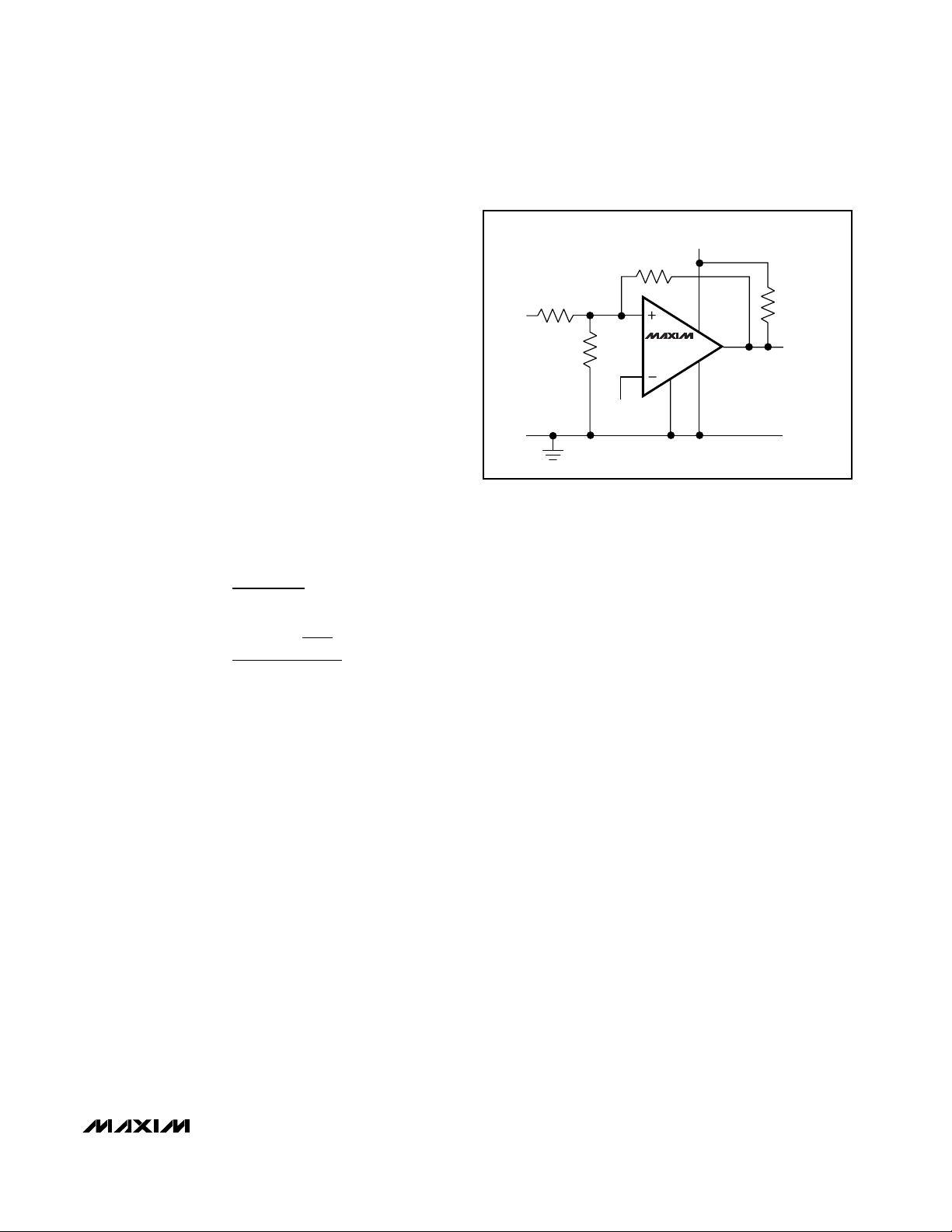
Typical Operating Circuit
19-0450; Rev 3; 2/03
Ordering Information continued at end of data sheet.
UCSP is a trademark of Maxim Integrated Products, Inc.
PART
INTERNAL
PRECISION
REFERENCE
INTERNAL
HYSTERESIS
PACKAGE
MAX971 1% Yes
8-Pin
DIP/SO/µMAX
MAX972 None No
8-Pin UCSP/
DIP/SO/µMAX
MAX973 1% Yes
8-Pin
DIP/SO/µMAX
MAX974
1% No 16-Pin DIP/SO
MAX981 2% Yes
8-Pin
DIP/SO/µMAX
MAX982 2% Yes
8-Pin
DIP/SO/µMAX
MAX983 2% Yes
8-Pin
DIP/SO/µMAX
MAX984 2% No 16-Pin DIP/SO
COMPARATORS
PER
PACKAGE
1
2
2
4
1
2
2
4
Ordering Information
For pricing, delivery, and ordering information, please contact Maxim/Dallas Direct! at
1-888-629-4642, or visit Maxim’s website at www.maxim-ic.com.
Battery-Powered
Systems
Threshold Detectors
Window Comparators
Level Translators
Oscillator Circuits
PART TEMP RANGE PIN-PACKAGE
MAX971CPA 0°C to +70°C 8 Plastic Dip
MAX971CSA 0°C to +70°C 8 SO
MAX971CUA 0°C to +70°C 8 µMAX
V
IN
7
V+
3
IN+
IN-
4
HYST
5
REF
6
V-
THRESHOLD DETECTOR
MAX971
MAX981
21
GND
OUT
8
MAX971–MAX974/MAX981–MAX984
Ultra-Low-Power, Open-Drain,
Single/Dual-Supply Comparators
2 _______________________________________________________________________________________
V+ to V-, V+ to GND, GND to V-................................-0.3V, +12V
Inputs
Current: IN_+, IN_-, HYST..............................................20mA
Voltage: IN_+, IN_-, HYST ...............(V+ + 0.3V) to (V- - 0.3V)
Outputs
Current: REF...................................................................20mA
OUT_ ................................................................50mA
Voltage: REF ....................................(V+ + 0.3V) to (V- - 0.3V)
OUT_ (MAX9_1/9_4)..................12V to (GND - 0.3V)
(MAX9_2/9_3).......................12V to (V- - 0.3V)
OUT_ Short-Circuit Duration ..................................Continuous
Continuous Power Dissipation (T
A
= +70°C)
8-Bump UCSP (derate 4.7mW/°C above +70°C) ........379mW
8-Pin Plastic DIP (derate 9.09mW/°C above +70°C) ...727mW
8-Pin SO (derate 5.88mW/°C above +70°C)................471mW
8-Pin µMAX (derate 4.1mW/°C above +70°C) .............330mW
16-Pin Plastic DIP (derate 10.53mW/°C above +70°C)..842mW
16-Pin SO (derate 8.70mW/°C above +70°C) ................696mW
Operating Temperature Ranges
MAX97_C_ _/MAX98_C_ _..................................0°C to +70°C
MAX97_E_ _/MAX98_E_ _ ...............................-40°C to +85°C
Storage Temperature Range .............................-65°C to +150°C
Lead Temperature (soldering, 10s) .................................+300°C
Bump Temperature (soldering)
Reflow ..........................................................................+235°C
ELECTRICAL CHARACTERISTICS—5V OPERATION
(V+ = 5V, V- = GND = 0V, TA= T
MIN
to T
MAX
, unless otherwise noted. Typical values are at TA= +25°C.) (Note 1)
Stresses beyond those listed under “Absolute Maximum Ratings” may cause permanent damage to the device. These are stress ratings only, and functional
operation of the device at these or any other conditions beyond those indicated in the operational sections of the specifications is not implied. Exposure to
absolute maximum rating conditions for extended periods may affect device reliability.
ABSOLUTE MAXIMUM RATINGS
POWER REQUIREMENTS
Supply Voltage Range (Note 2) 2.5 11 V
Output Voltage Range 0 11 V
Supply Current
COMPARATOR
Input Offset Voltage VCM = 2.5V ±10 mV
Input Leakage Current (IN-, IN+) IN+ = IN- = 2.5V C/E temp ranges ±0.01 ±5 nA
Input Leakage Current (HYST) MAX9_1/MAX982/MAX9_3 ±0.02 nA
Input Common-Mode Voltage
Range
Common-Mode Rejection Ratio V- to (V+ - 1.3V) 0.1 1.0 mV/V
Power-Supply Rejection Ratio V+ = 2.5V to 11V 0.1 1.0 mV/V
Voltage Noise 100Hz to 100kHz 20 µV
Hysteresis Input Voltage Range MAX9_1/MAX982/MAX9_3 REF - 0.05 REF V
Response Time (High-to-Low
Transition)
Response Time (Low-to-High
Transition) (Note 3)
PARAMETER CONDITIONS MIN TYP MAX UNITS
MAX9_1,
HYST = REF
IN+ = IN- +
100mV
TA = +25°C, 100pF load,
1MΩ pullup to V+
= +25°C, 100pF load, 1MΩ pullup to V+ 300 µs
T
A
MAX972
MAX982/
MAX9_3,
HYST = REF
MAX9_4
TA = +25°C 2.5 3.2
C/E temp ranges 4
TA = +25°C 2.5 3.2
C/E temp ranges 4
TA = +25°C 3.1 4.5
C/E temp ranges 6
TA = +25°C 5.5 6.5
C/E temp ranges 8.5
V- V+ - 1.3 V
Overdrive = 10mV 12
Overdrive = 100mV 4
µA
RMS
µs
MAX971–MAX974/MAX981–MAX984
Ultra-Low-Power, Open-Drain,
Single/Dual-Supply Comparators
_______________________________________________________________________________________ 3
ELECTRICAL CHARACTERISTICS—5V OPERATION (continued)
(V+ = 5V, V- = GND = 0V, TA= T
MIN
to T
MAX
, unless otherwise noted. Typical values are at TA= +25°C.) (Note 1)
ELECTRICAL CHARACTERISTICS—3V OPERATION
(V+ = 3V, V- = GND = 0V, TA= T
MIN
to T
MAX
, unless otherwise noted. Typical values are at TA= +25°C.) (Note 1)
Output Low Voltage
Output Leakage Current V
REFERENCE (MAX9_1/MAX982/MAX9_3/MAX9_4 ONLY)
Reference Voltage
Source Current
Sink Current
Voltage Noise 100Hz to 100kHz 100 µV
PARAMETER CONDITIONS MIN TYP MAX UNITS
MAX9_2/MAX9_3, I
MAX9_1/MAX9_4, I
= 11V 100 nA
OUT
MAX971/MAX973/
MAX974
MAX981–MAX984
TA = +25°C1525
C/E temp ranges 6
TA = +25°C815
C/E temp ranges 4
= 1.8mA V- + 0.4
OUT
= 1.8mA
OUT
C temp range 1% 1.170 1.182 1.194
E temp range 2% 1.158 1.206
C temp range 2% 1.158 1.182 1.206
E temp range 3% 1.147 1.217
GND
+ 0.4
POWER REQUIREMENTS
Supply Current
COMPARATOR
Input Offset Voltage VCM = 1.5V ±10 mV
Input Leakage Current (IN-, IN+) IN+ = IN- = 1.5V C/E temp ranges ±0.01 ±5 nA
Input Leakage Current (HYST) MAX9_1/MAX982/MAX9_3 ±0.02 nA
Input Common-Mode Voltage
Range
Common-Mode Rejection Ratio V- to (V+ - 1.3V) 0.2 1 mV/V
Power-Supply Rejection Ratio V+ = 2.5V to 11V 0.1 1 mV/V
Voltage Noise 100Hz to 100kHz 20 µV
Hysteresis Input Voltage Range MAX9_1/MAX982/MAX9_3 REF - 0.05 REF V
PARAMETER CONDITIONS MIN TYP MAX UNITS
TA = +25°C 2.4 3.0
C/E temp ranges 3.8
TA = +25°C 2.4 3.0
C/E temp ranges 3.8
TA = +25°C 3.4 4.3
C/E temp ranges 5.8
TA = +25°C 5.2 6.2
C/E temp ranges 8.0
V- V+ - 1.3 V
HYST = REF,
IN+ = (IN- +
100mV)
MAX9_1
MAX972
MAX982/
MAX9_3
MAX9_4
V
V
µA
µA
RMS
µA
RMS
MAX971–MAX974/MAX981–MAX984
Ultra-Low-Power, Open-Drain,
Single/Dual-Supply Comparators
4 _______________________________________________________________________________________
ELECTRICAL CHARACTERISTICS—3V OPERATION (continued)
(V+ = 3V, V- = GND = 0V, TA= T
MIN
to T
MAX
, unless otherwise noted. Typical values are at TA= +25°C.) (Note 1)
Note 1: The MAX972EBL is 100% tested at T
A
= +25°C. Temperature limits are guaranteed by design.
Note 2: MAX974/MAX984 comparators work below 2.5V; see Low-Voltage Operation section for more details.
Note 3: Low-to-high response time is the result of the 1MΩ pullup and the 100pF capacitive load, based on three time constants.
A faster response time is achieved with a smaller RC.
Response Time (High-to-Low
Transition)
Response Time (Low-to-High
Transition) (Note 3)
Output Low Voltage
Output Leakage Current V
REFERENCE
Reference Voltage
Source Current
Sink Current
Voltage Noise 100Hz to 100kHz 100 µV
PARAMETER CONDITIONS MIN TYP MAX UNITS
TA = +25°C, 100pF load,
1MΩ pullup to V+
T
= +25°C, 100pF load, 1MΩ pullup to V+ 300 µs
A
MAX9_2/MAX9_3, I
MAX9_1/MAX9_4, I
= 11V 100 nA
OUT
MAX971/MAX973/
MAX974
MAX981–MAX984
TA = +25°C1525
C/E temp ranges 6
TA = +25°C815
C/E temp ranges 4
OUT
OUT
Overdrive = 10mV 12
Overdrive = 100mV 4
= 0.8mA V- + 0.4
= 0.8mA GND + 0.4
C temp range 1% 1.170 1.182 1.194
E temp range 2% 1.158 1.206
C temp range 2% 1.158 1.182 1.206
E temp range 3% 1.147 1.217
µs
V
V
µA
µA
RMS
MAX971–MAX974/MAX981–MAX984
Ultra-Low-Power, Open-Drain,
Single/Dual-Supply Comparators
_______________________________________________________________________________________ 5
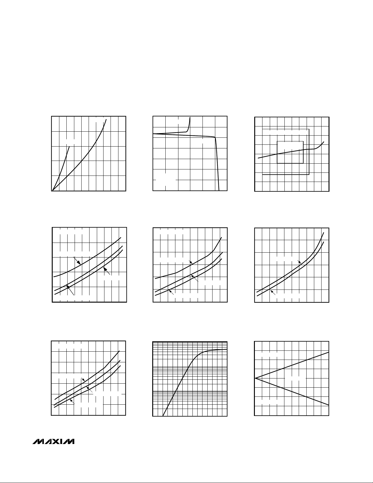
__________________________________________Typical Operating Characteristics
(V+ = 5V, V- = GND = 0V, TA = +25°C, unless otherwise noted.)
0
020
OUTPUT VOLTAGE LOW
vs. LOAD CURRENT
0.5
2.5
MAX971-4/981-4-TOC1
LOAD CURRENT (mA)
V
OL
(V)
12
1.5
1.0
48 16
2.0
V+ = 5V
V+ = 3V
1.155
0 5 15 25
REFERENCE OUTPUT VOLTAGE vs.
OUTPUT LOAD CURRENT
1.165
1.185
MAX971-4/981-4 TOC2
OUTPUT LOAD CURRENT (µA)
REFERENCE OUTPUT VOLTAGE (V)
10 20
1.175
1.190
1.160
1.180
1.170
V+ = 5V
OR
V+ = 3V
30
SINK
SOURCE
1.22
1.14
-60 -20 60 140
MAX971/MAX973/MAX974
REFERENCE VOLTAGE vs. TEMPERATURE
1.16
1.20
MAX971-4/981-4 TOC3
TEMPERATURE (°C)
REFERENCE VOLTAGE (V)
20 100
1.18
1.21
1.15
1.19
1.17
-40 0 8040 120
EXTENDED TEMP RANGE
COMMERCIAL
TEMP RANGE
MAX9_1
SUPPLY CURRENT vs.
TEMPERATURE
4.5
IN+ = IN- + 100mV
4.0
V+ = 5V, V- = - 5V
3.5
3.0
SUPPLY CURRENT (µA)
2.5
2.0
V+ = 5V, V- = 0V
-20 20 100
-60 140
TEMPERATURE (°C)
V+ = 3V, V- = 0V
60
4.5
4.0
MAX971-4/981-4 TOC4
3.5
3.0
2.5
SUPPLY CURRENT (µA)
2.0
1.5
SUPPLY CURRENT vs. TEMPERATURE
IN+ = (IN- + 100mV)
V+ = 10V, V- = 0V
-60 140
MAX972
V+ = 5V, V- = 0V
V+ = 3V, V- = 0V
-20 20 100
TEMPERATURE (°C)
60
5.0
4.5
MAX971-4/981-4 TOC5
4.0
3.5
3.0
SUPPLY CURRENT (µA)
2.5
2.0
SUPPLY CURRENT vs. TEMPERATURE
MAX982/MAX9_3
V+ = 5V, V- = 0V
V+ = 3V, V- = 0V
-20 20 100
-60 140
TEMPERATURE (°C)
60
MAX971-4/981-4 TOC6
SUPPLY CURRENT vs. TEMPERATURE
MAX9_4
10
IN+ = (IN- + 100mV)
9
8
7
V+ = 5V, V- = -5V
6
5
SUPPLY CURRENT (µA)
4
3
-60 140
V+ = 3V, V- = 0V
-20 20 100
TEMPERATURE (°C)
V+ = 5V, V- = 0V
60
MAX971-4/981-4 TOC7
MAX9_4
SUPPLY CURRENT vs.
LOW SUPPLY VOLTAGES
10
1
0.1
SUPPLY CURRENT (µA)
0.01
1.0 2.0 2.5
1.5
SINGLE-SUPPLY VOLTAGE (V)
MAX971-4/981-4 TOC8
IN+ - IN- (V)
-20
-40
-60
-80
MAX9_1/MAX982/MAX9_3
HYSTERESIS CONTROL
80
60
OUTPUT HIGH
40
20
0
OUTPUT LOW
010 30 50
NO CHANGE
20 40
V
- V
HYST
(mV)
REF
MAX971-4/981-4 TOC9
Ultra-Low-Power, Open-Drain,
Single/Dual-Supply Comparators
6 _______________________________________________________________________________________
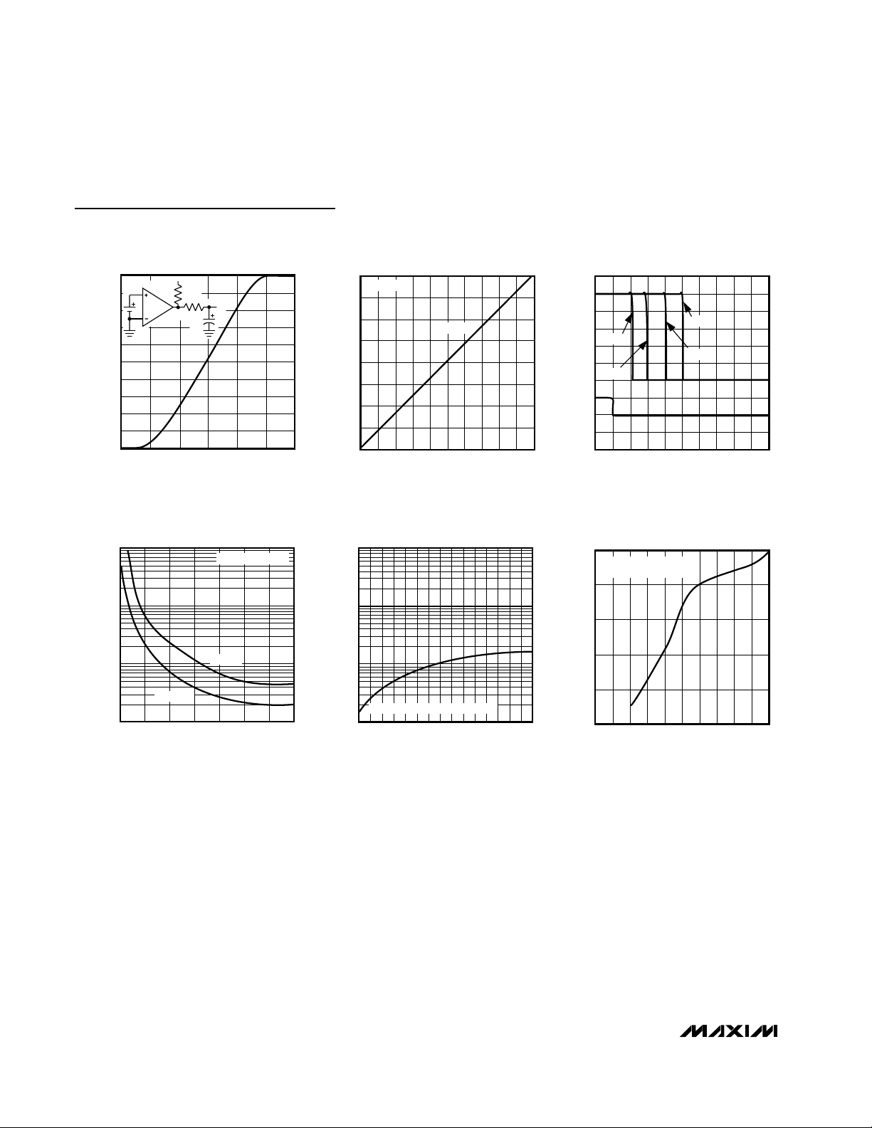
Typical Operating Characteristics (continued)
(V+ = 5V, V- = GND = 0V, TA = +25°C, unless otherwise noted.)
1000
1
1.0 2.0 2.2 2.4
RESPONSE TIME
AT LOW SUPPLY VOLTAGES (V
OHL
)
10
100
MAX971-4/981-4 TOC13
SINGLE-SUPPLY VOLTAGE (V)
RESPONSE TIME (µs)
1.2 1.4 1.6 1.8
-20mV
-100mV
R
PULLUP
= 10kΩ
100
0.1
1.0 2.0 2.5
MAX9_4
SINK CURRENT
AT LOW SUPPLY VOLTAGES
1
10
MAX971-4/981-4 TOC14
SINGLE-SUPPLY VOLTAGE (V)
CURRENT (mA)
1.5
SINK CURRENT AT V
OUT
= 0.4V
20
15
0
010
SHORT-CIRCUIT SINK CURRENT
vs. SUPPLY VOLTAGE
MAX971-4/981-4 TOC15
TOTAL SUPPLY VOLTAGE (V)
SINK CURRENT (mA)
5
10
5
25
OUT CONNECTED TO V+
GND CONNECTED TO V-
5.0
0
-0.3 -0.1 0.3
MAX9_1/MAX972/MAX9_4
TRANSFER FUNCTION
1.0
4.0
MAX971-4/981-4 TOC10
IN+ INPUT VOLTAGE (mV)
OUTPUT VOLTAGE (V)
0.1
3.0
2.0
4.5
0.5
3.5
2.5
1.5
-0.2 0
0.2
100kΩ
+5V
10kΩ
V
0
10µF
18
2
0 20 60 100
RESPONSE TIME vs.
LOAD CAPACITANCE
6
14
MAX971-4/981-4 TOC11
LOAD CAPACITANCE (nF)
RESPONSE TIME (µs)
40 80
10
16
4
12
8
V- = 0V
V
OHL
-2 2 10 18
RESPONSE TIME FOR VARIOUS
INPUT OVERDRIVES (V
OHL
)
0
4
MAX971-4/981-4 TOC12
RESPONSE TIME (µs)
V
OUT
(V)
614
2
0
5
100
3
1
50mV
100mV
20mV
10mV
V
IN
(mV)
MAX971–MAX974/MAX981–MAX984
Ultra-Low-Power, Open-Drain,
Single/Dual-Supply Comparators
_______________________________________________________________________________________ 7
Pin Description
PIN
MAX971/
MAX981
DIP/SO/
µMAX
1 —— — — GND
2 2 C2 2 2 V-
3 —— — — IN+ Noninverting Comparator Input
4 —— — — IN- Inverting Comparator Input
5 —— 5 5 HYST
6 —— 6 6 REF Reference Output. 1.182V with respect to V-.
7 7 A2 7 7 V+ Positive Supply
8 —— — — OUT Comparator Output. Sinks current to GND.
— 1 A1 1 1 OUTA Comparator A Open-Drain Output. Sinks current to V-.
— 3 C1 3 3 INA+ Noninverting Input of Comparator A
— 4B1—— INA- Inverting Input of Comparator A
— 5B3— 4 INB- Inverting Input of Comparator B
— 6C3 4 — INB+ Noninverting Input of Comparator B
— 8 A3 8 8 OUTB Comparator B Open-Drain Output. Sinks current to V-.
MAX972 MAX982
DIP/SO/
µMAX
UCSP
DIP/SO/
µMAX
MAX973/
MAX983
DIP/SO/
µMAX
NAME FUNCTION
Ground. Connect to V- for single-supply operation.
Negative Supply. Connect to GND for single-supply
operation (MAX9_1).
Hysteresis Input. Connect to REF if not used. Input
voltage range is from V
REF
to (V
REF
- 50mV).
MAX971–MAX974/MAX981–MAX984
Ultra-Low-Power, Open-Drain,
Single/Dual-Supply Comparators
8 _______________________________________________________________________________________
Pin Description (continued)
Comparator C Open-Drain Output. Sinks current to GND. OUTC16
Comparator D Open-Drain Output. Sinks current to GND.OUTD15
Ground. Connect to V- for single-supply operation.GND14
Noninverting Input of Comparator DIND+13
Inverting Input of Comparator DIND-12
Noninverting Input of Comparator CINC+11
Inverting Input of Comparator CINC-10
Negative Supply. Connect to ground for single-supply operation.V-9
Reference Output. 1.182V with respect to V-.REF8
Noninverting Input of Comparator BINB+7
Inverting Input of Comparator BINB-6
Noninverting Input of Comparator AINA+5
Inverting Input of Comparator AINA-4
Positive SupplyV+3
Comparator A Open-Drain Output. Sinks current to GND. OUTA2
Comparator B Open-Drain Output. Sinks current to GND. OUTB1
FUNCTIONNAME
PIN
MAX974
MAX984

MAX971–MAX974/MAX981–MAX984
Ultra-Low-Power, Open-Drain,
Single/Dual-Supply Comparators
_______________________________________________________________________________________ 9
Detailed Description
The MAX971–MAX974/MAX981–MAX984 comprise
various combinations of a micropower 1.182V reference
and micropower comparators. The Typical Operating
Circuit shows the MAX971/MAX981 configuration, and
Figures 1a–1d show the MAX9_2–MAX9_4 configurations.
Internal hysteresis in the MAX9_1, MAX982, and
MAX9_3 provides the easiest method for implementing
hysteresis. It also produces faster hysteresis action and
consumes much less current than circuits using external
positive feedback.
Power-Supply and Input Signal Ranges
This family of devices operates from a single 2.5V to 11V
power supply. The MAX9_1 and MAX9_4 have a
separate ground for the output driver, allowing operation
with dual supplies ranging from ±1.25V to ±5.5V.
Connect V- to GND when operating the MAX9_1 or
MAX9_4 from a single supply. The maximum total supply
voltage in this case is still 11V.
For proper comparator operation, the input signal can
range from the negative supply (V-) to within one volt of
the positive supply (V+ - 1V). The guaranteed commonmode input voltage range extends from V- to (V+ -
1.3V). The inputs can be taken above and below the
supply rails by up to 300mV without damage.
Figure 1a. MAX972 Functional Diagram
Figure 1c. MAX973/MAX983 Functional Diagram
(Window Comparator)
Figure 1b. MAX982 Functional Diagram
Figure 1d. MAX974/MAX984 Functional Diagram
1 (A1)
2 (C2)
3 (C1)
4 (B1)
OUTA
V-
INA+
INA-
MAX972
OUTB
INB+
INB-
8 (A3)
7 (A2)
V+
6 (C3)
5 (B3)
V-
MAX9_3
OUTB
REF
HYST
8
V+
7
6
5
OUTA
1
2
V-
INA+
3
INB-
4
( ) BUMPS FOR THE UCSP
OUTA
1
2
V-
INA+
3
INB+
4
MAX982
V-
OUTB
REF
HYST
OUTB
1
OUTA
2
V+
3
INA-
8
V+
7
6
5
4
INA+
5
6
INB-
7
INB+
8
REF
MAX9_4
OUTC
OUTD
GND
IND+
IND-
INC+
INC-
16
15
14
13
12
11
10
9
V-

MAX971–MAX974/MAX981–MAX984
Ultra-Low-Power, Open-Drain,
Single/Dual-Supply Comparators
10 ______________________________________________________________________________________
Low-Voltage Operation: V+ = 1V
(MAX9_4 Only)
The guaranteed minimum operating voltage is 2.5V (or
±1.25V). As the total supply voltage falls below 2.5V,
performance degrades and the supply current falls. The
reference will not function below about 2.2V, although
the comparators will continue to operate with a total
supply voltage as low as 1V. While the MAX9_4 has
comparators that may be used at supply voltages below
2V, the MAX9_1/MAX9_2/MAX9_3 may not be used with
supply voltages below 2.5V.
At low supply voltages, the comparators’ output sink
capability is reduced and the propagation delay
increases (see Typical Operating Characteristics). The
useful input voltage range extends from the negative
supply to a little under 1V below the positive supply,
which is slightly closer to the positive rail than when the
device operates from higher supply voltages. Test your
prototype over the full temperature and supply-voltage
range if you anticipate operation below 2.5V.
Comparator Output
With 100mV of overdrive, propagation delay is typically
3µs. The Typical Operating Characteristics show the
propagation delay for various overdrive levels. The
open-drain outputs are intended for wire-ORed and
level-shifting applications. The maximum output voltage
is 11V above V-, and may be applied even when no
supply voltage is present (V+ = V-).
The MAX9_1 and MAX9_4 outputs sink current to GND,
making these devices ideal for bipolar to single-ended
conversion and level-shifting applications.
The negative supply does not affect the output sink
current. The positive supply provides gate drive for the
output N-channel MOSFET and heavily influences the
output current capability, especially at low supply
voltages (see Typical Operating Characteristics section).
The MAX9_2 and MAX9_3 have no GND pin, and their
outputs sink current to V-.
Voltage Reference
The internal bandgap voltage reference has an output
of 1.182V above V-. Note that the REF voltage is
referenced to V-, not to GND. Its accuracy is ±1%
(MAX971/MAX973/MAX974) or ±2% (MAX981–MAX984)
in the 0°C to +70°C range. The REF output is typically
capable of sourcing 25µA and sinking 15µA. Do not
bypass the REF output.
Noise Considerations
Although the comparators have a very high gain, useful
gain is limited by noise. This is shown in the Transfer
Function graph (see Typical Operating Characteristics).
As the input voltage approaches the comparator’s
offset, the output begins to bounce back and forth; this
peaks when V
IN
= VOS. (The lowpass filter shown on the
graph averages out the bouncing, making the transfer
function easy to observe.) Consequently, the
comparator has an effective wideband peak-to-peak
noise of around 300µV. The voltage reference has
peak-to-peak noise approaching 1mV. Thus, when a
comparator is used with the reference, the combined
peak-to-peak noise is about 1mV. This, of course, is
much higher than the RMS noise of the individual
components. Take care in your layout to avoid
capacitive coupling from any output to the reference
pin. Crosstalk can significantly increase the actual
noise of the reference.
Figure 2. Threshold Hysteresis Band
Figure 3. Programming the HYST Pin
IN+
IN-
V
- V
REF
HYST
OUT
V
HB
THRESHOLDS
HYSTERESIS
BAND
I
REF
R1
R2
2.5V TO 11V
7
6
5
REF
HYST
2
V+
MAX9_1
MAX982
MAX9_3
V-
MAX971–MAX974/MAX981–MAX984
Ultra-Low-Power, Open-Drain,
Single/Dual-Supply Comparators
______________________________________________________________________________________ 11
__________Applications Information
Hysteresis
Hysteresis increases the comparators’ noise margin by
increasing the upper threshold and decreasing the
lower threshold (Figure 2).
Hysteresis (MAX9_1/MAX982/MAX9_3)
To add hysteresis to the MAX9_1, MAX982, or MAX9_3,
connect resistor R1 between REF and HYST, and
connect resistor R2 between HYST and V- (Figure 3). If
no hysteresis is required, connect HYST to REF. When
hysteresis is added, the upper threshold increases by
the same amount that the lower threshold decreases.
The hysteresis band (the difference between the upper
and lower thresholds, VHB) is approximately equal to
twice the voltage between REF and HYST. The HYST
input can be adjusted to a maximum voltage of REF
and to a minimum voltage of (REF - 50mV). The
maximum difference between REF and HYST (50mV)
will therefore produce a 100mV (max) hysteresis band.
Use the following equations to determine R1 and R2:
where I
REF
(the current sourced by the reference)
should not exceed the REF source capability, and
should be significantly larger than the HYST input
current. I
REF
values between 0.1µA and 4µA are usually
appropriate. If 2.4MΩ is chosen for R2 (I
REF
= 0.5µA),
the equation for R1 and VHBcan be approximated as:
When hysteresis is obtained in this manner for the
MAX982/MAX9_3, the same hysteresis applies to both
comparators.
Hysteresis (MAX972/MAX9_4)
Hysteresis can be implemented with any comparator
using positive feedback, as shown in Figure 4. This
approach generally draws more current than circuits
using the HYST pin on the MAX9_1/MAX982/MAX9_3,
and the high feedback impedance slows hysteresis. In
addition, because the output does not source current,
any increase in the upper threshold is dependent on
the load or pullup resistor on the output.
Board Layout and Bypassing
Power-supply bypass capacitors are not needed if the
supply impedance is low, but 100nF bypass capacitors
should be used when the supply impedance is high or
when the supply leads are long. Minimize signal lead
lengths to reduce stray capacitance between the input
and output that might cause instability. Do not bypass
the reference output.
Window Detector
The MAX9_3 is ideal for making window detectors
(undervoltage/overvoltage detectors). The schematic is
shown in Figure 5, with component values selected for a
4.5V undervoltage threshold and a 5.5V overvoltage
threshold. Choose different thresholds by changing the
values of R1, R2, and R3. To prevent chatter at the
output when the supply voltage is close to a threshold,
hysteresis has been added using R4 and R5. Taken
alone, OUTA would provide an active-low undervoltage
indication, and OUTB would give an active-low
overvoltage indication. Wired-ORing the two outputs
provides an active-high, power-good signal.
The design procedure is as follows:
1) Choose the required hysteresis level and calculate
values for R4 and R5 according to the formulas in
the Hysteresis (MAX9_1/MAX982/MAX9_3) section.
In this example, ±5mV of hysteresis has been added
at the comparator input (V
H
= VHB/2). This means
that the hysteresis apparent at VINwill be larger
because of the input resistor divider.
Figure 4. External Hysteresis
R1 =
R2 =
R1 (k ) = V (mV)
V
HB
2 I
×
()
REF
1.182 –
Ω
I
HB
REF
V
HB
2
V+
R
H
R
V
IN
V
REF
MAX9_4
GND
V+
OUT
V-
PULLUP

MAX971–MAX974/MAX981–MAX984
Ultra-Low-Power, Open-Drain,
Single/Dual-Supply Comparators
12 ______________________________________________________________________________________
2) Select R1. The leakage current into INB- is normally
under 1nA, so the current through R1 should exceed
100nA for the thresholds to be accurate. R1 values
up to about 10MΩ can be used, but values in the
100kΩ to 1MΩ range are usually easier to deal with.
In this example, choose R1 = 294kΩ.
3) Calculate R2 + R3. The overvoltage threshold
should be 5.5V when VINis rising. The design
equation is as follows:
4) Calculate R2. The undervoltage threshold should be
4.5V when VINis falling. The design equation is as
follows:
5) Calculate R3:
Choose R3 = 1MΩ (1% standard value)
6) Verify the resistor values. The equations are as
follows, evaluated for the above example:
Battery Switchover Circuit
The switchover from line-powered DC to a backup
battery is often accomplished with diodes. But this
simple method is sometimes unacceptable, due to the
voltage drop and associated power loss across the
diode in series with the battery. Figure 6’s circuit
replaces the diode with a P-channel MOSFET
controlled by one of the MAX9_3 comparator outputs.
When the DC wall adapter drops below 4V (determined
by R1 and R2), OUTA goes low, turning on Q1.
Comparator B is used to measure the battery voltage,
and gives a “low-battery” indication when the battery
drops below 3.6V.
Level-Shifter
Figure 7 shows a circuit to shift from bipolar ±5V inputs
to single-ended 5V outputs. The 10kΩ resistors protect
the comparator inputs, and do not materially affect the
circuit’s operation.
Figure 5. Window Detector
R3
1MΩ
RR R
231 1
+=×
=Ω×
=Ω
RRRR
2123 1
( + + )
=×−−
kM
294 1 068
( + . )
=Ω Ω×
=Ω
Choose R k s dard value
k
294
−Ω
k
62 2
.
26191
=Ω
. (% ).
V
OTH
VV
+
REF H
k
294
1 068
.
1 182 0 005
(. . )
M
VV
( )
REF H
V
(. . )
tan
−
55
.
+
R
−
45
.
UTH
1 182 0 005
1
−
R2
62.2kΩ
R1
294kΩ
RRRR
3232
( + )
=−
Mk
1 068 61 9
. .
=Ω−Ω
M
1 006
.
=Ω
Overvoltage Threshold:
++
=+×
V (V V )
OTH REF H
=
5.474V
Undervoltage Threshold:
=−×
V (V V )
UTH REF H
=
4.484V
where the hysteresis voltage V V
(R1 R2 R3)
R1
++
(R1 R2 R3)
(R1 + R2)
=×
H REF
R5
R4
.
V
10kΩ
R4
2.4MΩ
= 5.5V
OTH
= 4.5V
V
UTH
3
5
R5
6
4
V
IN
5V
INA+
HYST
REF
INB-
7
V+
OUTA
OUTB
V-
2
MAX9_3
1MΩ
1
8
POWER GOOD

MAX971–MAX974/MAX981–MAX984
Ultra-Low-Power, Open-Drain,
Single/Dual-Supply Comparators
______________________________________________________________________________________ 13
Figure 6. Battery Switchover Circuit
Figure 7. Level Shifter: ±5V Input to Single-Ended 3.3V Output
UCSP Applications Information
For the latest application details on UCSP contruction,
dimensions, tape carrier information, printed circuit
board techniques, bump-pad layout and
recommended reflow temperature profile as well as the
latest information on reliability testing results, go to
Maxim’s web site at www.maxim-ic.com/ucsp to find
the Application Note: UCSP–A Wafer-Level Chip-Scale
Package.
WALL
ADAPTER
9V DC
R1
110kΩ
R2
47kΩ
Q1
BATTERY
(4 CELLS)
953kΩ
470kΩ
DC OK
1MΩ
3
5V 3.3V
3
V+
GND
MAX974
MAX984
914
OUTA 2
OUTB
OUTC
OUTD
REF
V-
1
16
15
8
N.C.
STEP-DOWN
REGULATOR
7
V+
MAX973
MAX983
4
INB-
OUTB
1
OUTA
INA+
REF
HYST
V2
8
LOW BATT
6
5
3.3V
LOGIC
SUPPLY
10kΩ
20kΩ
2.4MΩ
10kΩ
V
INA
10kΩ
V
INB
10kΩ
V
INC
10kΩ
V
IND
5
INA+
4
INA-
7
INB+
INB-
6
11
INC+
INC-
10
IND+
13
12
IND-
-5V

MAX971–MAX974/MAX981–MAX984
Ultra-Low-Power, Open-Drain,
Single/Dual-Supply Comparators
14 ______________________________________________________________________________________
Pin Configurations
TOP VIEW
GND
V-
IN+
1
2
MAX971
3
MAX981
4
DIP/SO/µMAX
8
OUT
V+
7
REF
6
HYSTIN-
5
OUTA
INA+
1
2
V-
MAX972
3
4
8
OUTB
V+
7
6
INB+
5
INB-INA-
DIP/SO/µMAX
TOP VIEW
(BUMPS ON BOTTOM)
12 3
OUTA
V-
INA+
1
2
MAX973
3
MAX983
4
DIP/SO/µMAX
A
OUTA
B
INA-
INA+
C
V+
MAX972
OUTB
INB-
INB+V-
8
OUTB
V+
7
REF
6
HYSTINB-
5
UCSP
OUTA
INA+
OUTB
OUTA
INA+
INB-
INB+
REF
1
2
V-
3
4
1
2
3
V+
4
5
6
7
8
MAX982
DIP/SO/µMAX
MAX974
MAX984
DIP/Narrow SO
8
OUTB
V+
7
6
REF
5
HYSTINB+
16
OUTC
15
OUTD
14
GND
13
IND+INA-
12
IND-
11
INC+
10
INC-
V-
9
MAX971–MAX974/MAX981–MAX984
Ultra-Low-Power, Open-Drain,
Single/Dual-Supply Comparators
______________________________________________________________________________________ 15
*UCSP top mark is “ABC.”
Ordering Information (continued)
MAX971/MAX972/MAX973/MAX981/MAX982/MAX984
TRANSISTOR COUNT: 164
MAX974/MAX984 TRANSISTOR COUNT: 267
___________________Chip Information
PART TEMP RANGE PIN-PACKAGE
MAX971EPA -40°C to +85°C 8 Plastic Dip
MAX971ESA -40°C to +85°C 8 SO
MAX972CPA 0°C to +70°C 8 Plastic Dip
MAX972CSA 0°C to +70°C 8 SO
MAX972CUA 0°C to +70°C 8 µMAX
MAX972EBL-T* -40°C to +85°C 8 UCSP-8
MAX972EPA -40°C to +85°C 8 Plastic Dip
MAX972ESA -40°C to +85°C 8 SO
MAX973CPA 0°C to +70°C 8 Plastic Dip
MAX973CSA 0°C to +70°C 8 SO
MAX973CUA 0°C to +70°C 8 µMAX
MAX973EPA -40°C to +85°C 8 Plastic Dip
MAX973ESA -40°C to +85°C 8 SO
MAX974CPE 0°C to +70°C 16 Plastic Dip
MAX974CSE 0°C to +70°C 16 Narrow SO
MAX974EPE -40°C to +85°C 16 Plastic Dip
MAX974ESE -40°C to +85°C 16 Narrow SO
MAX981CPA 0°C to +70°C 8 Plastic Dip
PART TEMP RANGE PIN-PACKAGE
MAX981CSA 0°C to +70°C 8 SO
MAX981CUA 0°C to +70°C 8 µMAX
MAX981EPA -40°C to +85°C 8 Plastic Dip
MAX981ESA -40°C to +85°C 8 SO
MAX982CPA 0°C to +70°C 8 Plastic Dip
MAX982CSA 0°C to +70°C 8 SO
MAX982CUA 0°C to +70°C 8 µMAX
MAX982EPA -40°C to +85°C 8 Plastic Dip
MAX982ESA -40°C to +85°C 8 SO
MAX983CPA 0°C to +70°C 8 Plastic Dip
MAX983CSA 0°C to +70°C 8 SO
MAX983CUA 0°C to +70°C 8 µMAX
MAX983EPA -40°C to +85°C 8 Plastic Dip
MAX983ESA -40°C to +85°C 8 SO
MAX984CPE 0°C to +70°C 16 Plastic Dip
MAX984CSE 0°C to +70°C 16 Narrow SO
MAX984EPE -40°C to +85°C 16 Plastic Dip
MAX984ESE -40°C to +85°C 16 Narrow SO

SOICN .EPS
PACKAGE OUTLINE, .150" SOIC
1
1
21-0041
B
REV.DOCUMENT CONTROL NO.APPROVAL
PROPRIETARY INFORMATION
TITLE:
TOP VIEW
FRONT VIEW
MAX
0.010
0.069
0.019
0.157
0.010
INCHES
0.150
0.007
E
C
DIM
0.014
0.004
B
A1
MIN
0.053A
0.19
3.80 4.00
0.25
MILLIMETERS
0.10
0.35
1.35
MIN
0.49
0.25
MAX
1.75
0.050
0.016L
0.40 1.27
0.3940.386D
D
MINDIM
D
INCHES
MAX
9.80 10.00
MILLIMETERS
MIN
MAX
16
AC
0.337 0.344 AB8.758.55 14
0.189 0.197 AA5.004.80 8
N MS012
N
SIDE VIEW
H 0.2440.228 5.80 6.20
e 0.050 BSC 1.27 BSC
C
HE
e
B
A1
A
D
0∞-8∞
L
1
VARIATIONS:
MAX971–MAX974/MAX981–MAX984
Ultra-Low-Power, Open-Drain,
Single/Dual-Supply Comparators
16 ______________________________________________________________________________________
Package Information
(The package drawing(s) in this data sheet may not reflect the most current specifications. For the latest package outline information,
go to www.maxim-ic.com/packages
.)
0.6±0.1
0.6±0.1
A2
8
ÿ 0.50±0.1
1
D
TOP VIEW
e
FRONT VIEW
4X S
E H
BOTTOM VIEW
A1
A
c
b
L
SIDE VIEW
8
1
DIM
A
A1
A2
b
c
D
e
E
H
L
α
S
INCHES
MIN
-
0.002
0.030
0.010
0.005
0.116
0.0256 BSC
0.116
0.188
0.016
0∞
0.0207 BSC
MAX
0.043
0.006
0.037
0.014
0.007
0.120
0.120
0.198
0.026
6∞
MILLIMETERS
MIN
- 1.10
0.05 0.15
0.25 0.36
0.13 0.18
2.95 3.05
0.65 BSC
2.95 3.05
4.78
0.41
0.5250 BSC
MAX
0.950.75
5.03
0.66
8LUMAXD.EPS
6∞0∞
α
PROPRIETARY INFORMATION
TITLE:
PACKAGE OUTLINE, 8L uMAX/uSOP
21-0036
REV.DOCUMENT CONTROL NO.APPROVAL
1
J
1
MAX971–MAX974/MAX981–MAX984
Ultra Low-Power, Open-Drain,
Single/Dual-Supply Comparators
9LUCSP, 3x3.EPS
Package Information (continued)
(The package drawing(s) in this data sheet may not reflect the most current specifications. For the latest package outline information,
go to www.maxim-ic.com/packages
.)
Maxim cannot assume responsibility for use of any circuitry other than circuitry entirely embodied in a Maxim product. No circuit patent licenses are
implied. Maxim reserves the right to change the circuitry and specifications without notice at any time.
Maxim Integrated Products, 120 San Gabriel Drive, Sunnyvale, CA 94086 408-737-7600 ____________________ 17
© 2003 Maxim Integrated Products Printed USA is a registered trademark of Maxim Integrated Products.
PDIPN.EPS
 Loading...