

Page 1
General Description
The MAX9736A/B/D Class D amplifiers provide highperformance, thermally efficient amplifier solutions. The
MAX9736A delivers 2 x 15W into 8Ω loads, or 1 x 30W
into a 4Ω load. The MAX9736B/D deliver 2 x 6W into 8Ω
loads or 1 x 12W into a 4Ω load.
These devices operate from 8V to 28V and provide a
high PSRR, eliminating the need for a regulated power
supply. The MAX9736 offers up to 88% efficiency at
12V supply.
Pin-selectable modulation schemes select between filterless modulation and classic PWM modulation.
Filterless modulation allows the MAX9736 to pass CE
EMI limits with 1m cables using only a low-cost ferrite
bead and capacitor on each output. Classic PWM modulation is optimized for best audio performance when
using a full LC filter.
A pin-selectable stereo/mono mode allows stereo operation into 8Ω loads or mono operation into 4Ω loads. In
mono mode, the right input op amp becomes available
as a spare device, allowing flexibility in system design.
Comprehensive click-and-pop reduction circuitry minimizes noise coming into and out of shutdown or mute.
Input op amps allow the user to create summing amplifiers,
lowpass or highpass filters, and select an optimal gain.
The MAX9736A/B/D are available in 32-pin TQFN packages and specified over the -40°C to +85°C temperature range.
Features
o Wide 8V to 28V Supply Voltage Range
o Spread-Spectrum Modulation Enables Low EMI
Solution
o Passes CE EMI Limits with Low-Cost Ferrite
Bead/Capacitor Filter
o Low BOM Cost
o High 67dB PSRR at 1kHz Reduces Supply Cost
o 88% Efficiency Eliminates Heatsink
o Thermal and Output Current Protection
o < 1µA Shutdown Mode
o Mute Function
o Space-Saving, 32-Pin TQFN Packages, 7mm x
7mm x 0.8mm (MAX9736A/B), 5mm x 5mm x
0.8mm (MAX9736D)
MAX9736
Mono/Stereo High-Power Class D Amplifier
________________________________________________________________
Maxim Integrated Products
1
Ordering Information
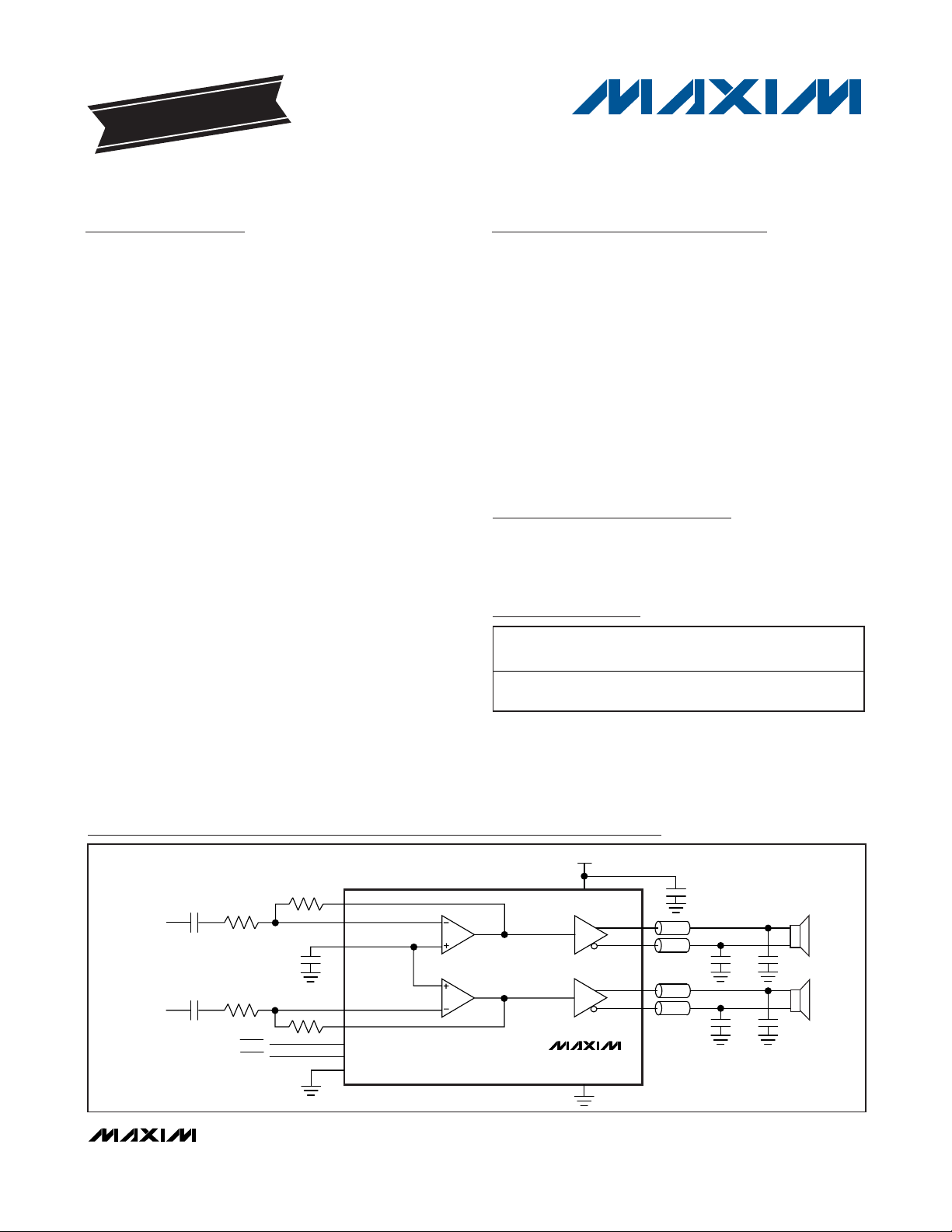
Applications
INPUT RESISTORS AND
CAPACITORS SELECT GAIN
AND CUTOFF FREQUENCY
AUDIO
INPUTS
SHDN
8Ω
8Ω
8V TO 28V
MAX9736
MUTE
MONO
Simplified Diagram
19-3108; Rev 3; 9/09
For pricing, delivery, and ordering information, please contact Maxim Direct at 1-888-629-4642,
or visit Maxim’s website at www.maxim-ic.com.
EVALUATION KIT
AVAILABLE
PART
STEREO/MONO
PIN-PACKAGE
MAX9736AETJ+
2 x 15W/
1 x 30W
32 TQFN-EP*
7mm x 7mm
Note: All devices are specified over the -40°C to +85°C operating temperature range.
+
Denotes a lead(Pb)-free/RoHS-compliant package.
*
EP = Exposed pad.
LCD/PDP/CRT Monitors
LCD/PDP/CRT TVs
MP3 Docking Stations
Notebook PCs
PC Speakers
All-in-One PCs
Ordering Information continued at end of data sheet.
OUTPUT POWER
Page 2
MAX9736
Mono/Stereo High-Power Class D Amplifier
2 _______________________________________________________________________________________
ABSOLUTE MAXIMUM RATINGS
ELECTRICAL CHARACTERISTICS
(V
PVDD
= 20V, VVS= 5V, V
AGND
= V
PGND
= 0V, V
MOD
= V
SHDN
= V
MUTE
= 5V, REGEN = MONO = AGND, C1 = 0.1μF, C2 = 1μF,
R
IN
_ = 20kΩ and R
FB_
= 20kΩ, RL= ∞, AC measurement bandwidth 22Hz to 22kHz, TA= T
MIN
to T
MAX
, unless otherwise noted.
Typical values are at T
A
= +25°C.) (Notes 4, 5)
Stresses beyond those listed under “Absolute Maximum Ratings” may cause permanent damage to the device. These are stress ratings only, and functional
operation of the device at these or any other conditions beyond those indicated in the operational sections of the specifications is not implied. Exposure to
absolute maximum rating conditions for extended periods may affect device reliability.
Note 1: VS cannot exceed PVDD + 0.3V. See the
Power Sequencing
section.
Note 2: Thermal performance of this device is highly dependant on PCB layout. See the
Applications Information
section for more details.
Note 3: Package thermal resistances were obtained using the method described in JEDEC specification JESD51-7, using a 4-layer
board. For detailed information on package thermal considerations, visit www.maxim-ic.com/thermal-tutorial
.
PVDD to PGND.......................................................-0.3V to +30V
AGND to PGND .....................................................-0.3V to +0.3V
INL, INR, FBL, FBR, COM to AGND .........-0.3V to (V
REG
+ 0.3V)
MUTE, SHDN, MONO, MOD, REGEN to AGND.......-0.3V to +6V
REG to AGND ..............................................-0.3V to (VS + 0.3V)
VS to AGND (Note 1)................................................-0.3V to +6V
OUTL+, OUTL-, OUTR+,
OUTR-, to PGND...................................-0.3V to (PVDD + 0.3V)
C1N to PGND ..........................................-0.3V to (PVDD + 0.3V)
C1P to PGND ...........................(PVDD - 0.3V) to (V
BOOT
+ 0.3V)
BOOT to PGND ..............................(V
C1P
- 0.3V) to PVDD + 12V
OUTL+, OUTL-, OUTR+, OUTR-,
Short Circuit to PGND or PVDD...............................Continuous
Thermal Limits (Notes 2, 3)
Continuous Power Dissipation (T
A
= +70°C)
32-Pin TQFN 5mm x 5mm Multiple Layer PCB
(derate 34.5mW/°C above +70°C)..................................2.76W
θ
JA
.................................................................................29°C/W
θ
JC
...................................................................................2°C/W
Continuous Power Dissipation (T
A
= +70°C)
32-Pin TQFN 7mm x 7mm Multiple Layer PCB
(derate 37mW/°C above +70°C).....................................2.96W
θ
JA
.................................................................................27°C/W
θ
JC
...................................................................................1°C/W
Operating Temperature Range ...........................-40°C to +85°C
Storage Temperature Range .............................-65°C to +150°C
Junction Temperature......................................................+150°C
Lead Temperature (soldering, 10s) .................................+300°C
PARAMETER SYMBOL CONDITIONS MIN TYP MAX UNITS
AMPLIFIER DC CHARACTERISTICS
Speaker Supply Voltage Range PVDD Inferred from PSRR test 8 28 V
Preamplifier Supply Voltage
Range
Undervoltage Lockout UVLO 7 V
Quiescent Supply Current
Shutdown Supply Current I
REG Voltage V
Preregulator Voltage VS Internal regulated 5V, V
COM Voltage V
INPUT AMPLIFIER CHARACTERISTICS
Capacitive Drive C
Output Swing (Note 6) Sinking ±1mA ±2 V
Open-Loop Gain A
Input Offset Voltage V
VS (Notes 1 and 7) 4.5 5.5 V
I
PVDD
I
VS
SHDN
REG
COM
VO
OS
L
RL = ∞, V
V
= open
VS
RL = ∞, V
V
= 5V
VS
V
= 0V
SHDN
V
= V
FB_
REGEN
REGEN
±500mV, R
COM
= 5V,
= 0V,
TA = +25°C 30 45
T
= T
MIN
to T
MAX
A
TA = +25°C 14 20
T
= T
A
I
PVDD
I
VS
REGEN
FB_
to T
MIN
MAX
= 5V 4.8 V
= 20kΩ to IN_ 88 dB
50
22
110
10
4.2 V
1.9 2.05 2.2 V
30 pF
±1 mV
mA
mA
μA
Page 3
MAX9736
ELECTRICAL CHARACTERISTICS (continued)
(V
PVDD
= 20V, VVS= 5V, V
AGND
= V
PGND
= 0V, V
MOD
= V
SHDN
= V
MUTE
= 5V, REGEN = MONO = AGND, C1 = 0.1μF, C2 = 1μF,
R
IN
_ = 20kΩ and R
FB_
= 20kΩ, RL= ∞, AC measurement bandwidth 22Hz to 22kHz, TA= T
MIN
to T
MAX
, unless otherwise noted.
Typical values are at T
A
= +25°C.) (Notes 4, 5)
Mono/Stereo High-Power Class D Amplifier
_______________________________________________________________________________________ 3
PARAMETER SYMBOL CONDITIONS MIN TYP MAX UNITS
Input Amplifier Slew Rate 2.5 V/μs
Input Amplifier Unity-Gain
Bandwidth
3.5 MHz
AMPLIFIER CHARACTERISTICS
Output Amplifier Gain (Note 8) A
MAX9736A, MAX9736D 16.5 17 17.5
V
MAX9736B 13.1 13.6 14.1
Output Current Limit 3.3 4.6 A
Output Offset V
OS
Power-Supply Rejection Ratio PSRR
MAX9736A Output Power
(THD+N = 1%)
MAX9736B Output Power
(THD+N = 1%)
MAX9736A Output Power
(THD+N = 10%)
MAX9736B Output Power
(THD+N = 10%)
P
OUT_1%
P
OUT_1%
P
OUT_10%
P
OUT_10%
OUT_+ to OUT_-, TA = +25°C ±2 ±10 mV
PVDD = 8V to 28V, TA = +25°C 65 80
f = 1kHz, 100mV
V
= 12V
P V D D
V
= 18V
P V D D
V
= 24V
P V D D
V
= 12V
P V D D
V
= 18V
P V D D
V
= 24V
P V D D
V
= 12V
P V D D
V
= 18V
P V D D
V
= 24V
P V D D
= 12V
P V D D
V
= 18V
P V D D
V
= 24V
P V D D
ripple 67
P-P
Stereo
Mono R
RL = 8Ω 8
= 4Ω 13
R
L
= 4Ω 15.5
L
Stereo RL = 8Ω 13.5
Mono R
= 4Ω 27
L
Stereo RL = 8Ω 13.5
Mono R
Stereo
Mono R
= 4Ω 27
L
RL = 8Ω 6
= 4Ω 11
R
L
= 4Ω 12
L
Stereo RL = 8Ω 6
Mono R
= 4Ω 12
L
Stereo RL = 8Ω 6
Mono R
Stereo
Mono R
= 4Ω 12
L
RL = 8Ω 10
= 4Ω 16
R
L
= 4Ω 19.5
L
Stereo RL = 8Ω 17.5
Mono R
= 4Ω 35
L
Stereo RL = 8Ω 17.5
Mono R
Stereo
Mono R
= 4Ω 35
L
RL = 8Ω 7.5
R
= 4Ω 14V
L
= 4Ω 15
L
Stereo RL = 8Ω 7.5
Mono R
= 4Ω 15
L
Stereo RL = 8Ω 7.5
Mono R
= 4Ω 15
L
dB
dB
W
W
W
W
Page 4
MAX9736
Mono/Stereo High-Power Class D Amplifier
4 _______________________________________________________________________________________
ELECTRICAL CHARACTERISTICS (continued)
(V
PVDD
= 20V, VVS= 5V, V
AGND
= V
PGND
= 0V, V
MOD
= V
SHDN
= V
MUTE
= 5V, REGEN = MONO = AGND, C1 = 0.1μF, C2 = 1μF,
R
IN
_ = 20kΩ and R
FB_
= 20kΩ, RL= ∞, AC measurement bandwidth 22Hz to 22kHz, TA= T
MIN
to T
MAX
, unless otherwise noted.
Typical values are at T
A
= +25°C.) (Notes 4, 5)
PARAMETER SYMBOL CONDITIONS MIN TYP MAX UNITS
MAX9736D Output Power
(Thermally Limited)
Total Harmonic Distortion Plus
Noise
Signal-to-Noise Ratio SNR A-weighted
Noise V
Crosstalk L to R, R to L, P
Efficiency η P
Click-and-Pop Level K
Switching Frequency 270 300 330 kHz
Spread-Spectrum Bandwidth ±4 kHz
Thermal Shutdown Level 160 °C
Thermal Shutdown Hysteresis 30 °C
Turn-On Time t
THD+N
N
CP
ON
V
= 12V
P V D D
V
= 18V
P V D D
V
= 24V
P V D D
MAX9736A, P
PWM modulation mode, R
MAX9736B/D, P
PWM modulation mode, R
A-weighted
(Note 9)
= 8W, M AX 9736A, P V D D = 12V , RL = 8Ω 88 %
OU T
Peak voltage, 32
samples/second,
A-weighted
(Notes 9 and 10)
Stereo RL = 8Ω 8.5
Mono R
= 4Ω 17
L
Stereo RL = 8Ω 5.5
Mono R
= 4Ω 11
L
Stereo RL = 8Ω 3.5
Mono R
= 4W, f = 1kHz,
OUT
= 2W, f = 1kHz,
OUT
= 4Ω 7
L
= 8Ω
L
= 8Ω
L
MAX9736A/D,
= 8W, RL = 8Ω
P
OUT
MAX9736B, P
= 8Ω
R
L
OUT
= 6W,
MAX9736A/D 120
MAX9736B 100
= 1W , f = 1kH z, RL = 8Ω 100 dB
OU T
Into mute 36
Out of mute 36
0.04
0.04
96.5
97
110 ms
μV
W
%
dB
RMS
dBV
Page 5
MAX9736
Mono/Stereo High-Power Class D Amplifier
_______________________________________________________________________________________ 5
ELECTRICAL CHARACTERISTICS (continued)
(V
PVDD
= 20V, VVS= 5V, V
AGND
= V
PGND
= 0V, V
MOD
= V
SHDN
= V
MUTE
= 5V, REGEN = MONO = AGND, C1 = 0.1μF, C2 = 1μF,
R
IN
_ = 20kΩ and R
FB_
= 20kΩ, RL= ∞, AC measurement bandwidth 22Hz to 22kHz, TA= T
MIN
to T
MAX
, unless otherwise noted.
Typical values are at T
A
= +25°C.) (Notes 4, 5)
Note 4: All devices are 100% production tested at +25°C. All temperature limits are guaranteed by design.
Note 5: Stereo mode (MONO = GND) specified with 8Ω resistive load in series with a 68μH inductive load connected across BTL
outputs. Mono mode (MONO = 5V) specified with a 4Ω resistive load in series with a 33μH inductive load connected
across BTL outputs.
Note 6: Output swing is specified with respect to V
COM.
Note 7: For typical applications, an external 5V supply is not required. Therefore, set REGEN = 5V. If thermal performance is a
concern, set REGEN = 0V and provide an external regulated 5V supply.
Note 8: Output amplifier gain is defined as:
Note 9: Amplifier inputs AC-coupled to GND.
Note 10: Specified at room temperature with an 8Ω resistive load in series with a 68μH inductive load connected across BTL outputs.
Mode transitions controlled by SHDN control pin.
PARAMETER SYMBOL CONDITIONS MIN TYP MAX UNITS
DIGITAL INTERFACE
Input Voltage High V
Input Voltage Low V
Input Voltage Hysteresis 50 mV
Input Leakage Current ±10 μA
20 ×
⎛
VV
|( ) ( )|
log
⎜
⎝
−
+−
OUT_ OUT
V
||
FB
_
INH
INL
_
2V
0.8 V
⎞
⎟
⎠
Page 6
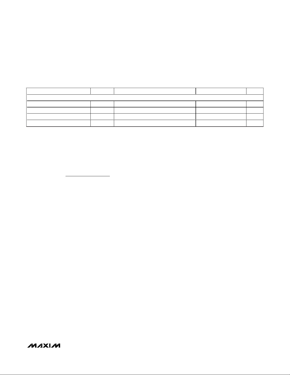
Typical Operating Characteristics
(MAX9736A, V
PVDD
= 12V, MOD = high, spread-spectrum modulation mode, V
GND
= V
PGND
= 0V, V
SHDN
= V
MUTE
= 5V, unless
otherwise noted.)
MAX9736
Mono/Stereo High-Power Class D Amplifier
6 _______________________________________________________________________________________
TOTAL HARMONIC DISTORTION
PLUS NOISE vs. FREQUENCY
1
V
= 12V,
PVDD
FIXED FREQUENCY,
8Ω LOAD
0.1
THD+N (%)
0.01
TOTAL HARMONIC DISTORTION
PLUS NOISE vs. FREQUENCY
1
V
= 12V,
PVDD
SPREAD SPECTRUM,
0.1
THD+N (%)
0.01
8Ω LOAD
P
OUT
= 5W
MAX9736 toc01
P
= 5W
OUT
P
= 3W
OUT
TOTAL HARMONIC DISTORTION
PLUS NOISE vs. FREQUENCY
1
V
= 12V,
PVDD
FIXED FREQUENCY,
0.1
THD+N (%)
0.01
4Ω LOAD
P
OUT
MAX9736 toc02
P
= 3W
OUT
= 5W
P
OUT
MAX9736 toc03
= 3W
0.001
10 100k
FREQUENCY (Hz)
TOTAL HARMONIC DISTORTION
PLUS NOISE vs. FREQUENCY
1
V
= 12V,
PVDD
SPREAD SPECTRUM,
4Ω LOAD
0.1
P
= 5W
OUT
THD+N (%)
0.01
0.001
10 100k
P
= 3W
OUT
FREQUENCY (Hz)
TOTAL HARMONIC DISTORTION
PLUS NOISE vs. OUTPUT POWER
10
V
= 18V,
PVDD
FIXED FREQUENCY,
8Ω LOAD
1
6kHz
0.001
10k1k100
10 100k
FREQUENCY (Hz)
10k1k100
TOTAL HARMONIC DISTORTION
PLUS NOISE vs. OUTPUT POWER
10
V
= 12V,
PVDD
MAX9736 toc04
10k1k100
FIXED FREQUENCY,
8Ω LOAD
1
6kHz
0.1
THD+N (%)
0.01
0.001
010
1kHz
20Hz
987654321
OUTPUT POWER (W)
TOTAL HARMONIC DISTORTION
PLUS NOISE vs. OUTPUT POWER
10
V
= 18V,
PVDD
MAX9736 toc07
SPREAD SPECTRUM,
8Ω LOAD
1
1kHz
6kHz
MAX9736 toc05
MAX9736 toc08
0.001
10 100k
FREQUENCY (Hz)
10k1k100
TOTAL HARMONIC DISTORTION
PLUS NOISE vs. OUTPUT POWER
10
V
= 12V,
PVDD
SPREAD SPECTRUM,
8Ω LOAD
1
1kHz
0.1
THD+N (%)
0.01
0.001
010
6kHz
20Hz
OUTPUT POWER (W)
MAX9736 toc06
987654321
TOTAL HARMONIC DISTORTION
PLUS NOISE vs. OUTPUT POWER
10
V
= 24V,
PVDD
FIXED FREQUENCY,
8Ω LOAD
1
6kHz
MAX9736 toc09
0.1
THD+N (%)
0.01
0.001
020
1kHz
20Hz
18161412108642
OUTPUT POWER (W)
0.1
THD+N (%)
0.01
0.001
020
20Hz
18161412108642
OUTPUT POWER (W)
0.1
THD+N (%)
0.01
0.001
0
OUTPUT POWER (W)
84
1kHz
20Hz
12
16
Page 7
Typical Operating Characteristics (continued)
(MAX9736A, V
PVDD
= 12V, MOD = high, spread-spectrum modulation mode, V
GND
= V
PGND
= 0V, V
SHDN
= V
MUTE
= 5V, unless
otherwise noted.)
MAX9736
Mono/Stereo High-Power Class D Amplifier
_______________________________________________________________________________________
7
TOTAL HARMONIC DISTORTION
PLUS NOISE vs. OUTPUT POWER
10
V
PVDD
SPREAD SPECTRUM,
8Ω LOAD
1
0.1
THD+N (%)
0.01
0.001
018
EFFICIENCY (%)
10
1
0.1
THD+N (%)
0.01
0.001
V
FIXED FREQUENCY,
4Ω LOAD
= 24V,
1kHz
OUTPUT POWER (W)
MAX9736 toc10
6kHz
20Hz
161412108642
EFFICIENCY
100
vs. TOTAL OUTPUT POWER
V
= 12V,
PVDD
90
FIXED FREQUENCY,
8Ω LOAD
80
70
60
50
40
30
20
10
0
020
EFFICIENCY
POWER DISSIPATION
TOTAL OUTPUT POWER (W)
15105
MAX9736 toc13
10
9
8
7
6
5
4
3
2
1
0
TOTAL HARMONIC DISTORTION
PLUS NOISE vs. OUTPUT POWER
= 12V,
PVDD
6kHz
1kHz
OUTPUT POWER (W)
POWER DISSIPATION (W)
20Hz
EFFICIENCY (%)
TOTAL HARMONIC DISTORTION
PLUS NOISE vs. OUTPUT POWER
10
V
= 12V,
PVDD
MAX9736 toc11
1412108642016
SPREAD SPECTRUM,
4Ω LOAD
1
6kHz
1kHz
0.1
THD+N (%)
0.01
0.001
018
OUTPUT POWER (W)
EFFICIENCY
100
V
PVDD
SPREAD SPECTRUM,
90
8Ω LOAD
80
70
60
50
40
30
20
10
0
vs. TOTAL OUTPUT POWER
= 12V,
EFFICIENCY
POWER DISSIPATION
TOTAL OUTPUT POWER (W)
MAX9736 toc14
181612 144 6 8 102020
20Hz
1512963
10
9
8
7
6
5
4
3
POWER DISSIPATION (W)
2
1
0
MAX9736 toc12
100
V
PVDD
90
SPREAD SPECTRUM,
8Ω LOAD
80
70
60
50
40
EFFICIENCY (%)
30
20
10
0
EFFICIENCY
vs. TOTAL OUTPUT POWER
= 18V,
EFFICIENCY
POWER DISSIPATION
TOTAL OUTPUT POWER (W)
MAX9736 toc15
10
9
8
7
6
5
4
3
POWER DISSIPATION (W)
2
1
0
302515 20105035
100
V
PVDD
90
FIXED FREQUENCY,
8Ω LOAD
80
70
60
50
40
EFFICIENCY (%)
30
20
10
0
EFFICIENCY
vs. TOTAL OUTPUT POWER
= 18V,
EFFICIENCY
POWER DISSIPATION
TOTAL OUTPUT POWER (W)
MAX9736 toc16
10
9
8
7
6
5
4
3
POWER DISSIPATION (W)
2
1
0
302515 20105035
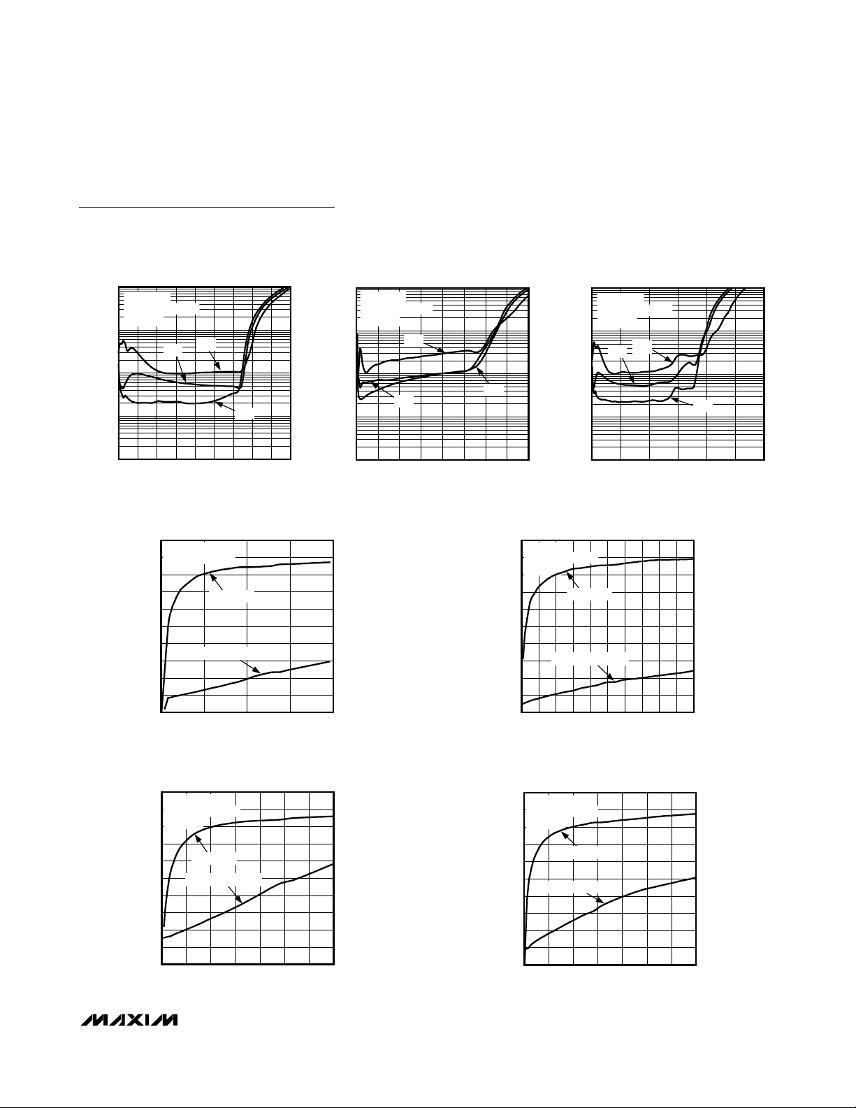
Page 8
Typical Operating Characteristics (continued)
(MAX9736A, V
PVDD
= 12V, MOD = high, spread-spectrum modulation mode, V
GND
= V
PGND
= 0V, V
SHDN
= V
MUTE
= 5V, unless
otherwise noted.)
MAX9736
Mono/Stereo High-Power Class D Amplifier
8 _______________________________________________________________________________________
100
EFFICIENCY (%)
EFFICIENCY
V
PVDD
90
FIXED FREQUENCY,
8Ω LOAD
80
70
60
50
40
30
20
10
0
vs. TOTAL OUTPUT POWER
= 24V,
EFFICIENCY
POWER DISSIPATION
TOTAL OUTPUT POWER (W)
MAX9736 toc17
2015105030
25
10
9
8
7
6
5
4
3
POWER DISSIPATION (W)
2
1
0
100
V
PVDD
90
SPREAD SPECTRUM,
8Ω LOAD
80
70
60
50
40
EFFICIENCY (%)
30
20
10
0
EFFICIENCY
vs. TOTAL OUTPUT POWER
= 24V,
EFFICIENCY
POWER DISSIPATION
2015105030
TOTAL OUTPUT POWER (W)
MAX9736 toc18
25
10
9
8
7
6
5
4
3
POWER DISSIPATION (W)
2
1
0
EFFICIENCY
100
V
= 12V,
PVDD
90
FIXED FREQUENCY,
4Ω LOAD
80
70
60
50
40
EFFICIENCY (%)
30
20
10
0
EFFICIENCY
POWER DISSIPATION
TOTAL OUTPUT POWER (W)
TOTAL OUTPUT POWER vs. V
LOAD = 8Ω, f = 1kHz
40
vs. TOTAL OUTPUT POWER
35
30
25
20
15
OUTPUT POWER (W)
10
10% THD+N
1% THD+N
5
0
530
SUPPLY VOLTAGE (V)
2510 2015
MAX9736 toc19
15105020
DD
MAX9736 toc21
10
9
8
7
6
5
4
3
POWER DISSIPATION (W)
2
1
0
TOTAL OUTPUT POWER vs. LOAD RESISTANCE
= 12V, f = 1kHz, SPREAD SPECTRUM
V
DD
16
14
12
10
8
6
OUTPUT POWER (W)
4
2
0
1% THD+N
530
10% THD+N
LOAD RESISTANCE (Ω)
100
V
PVDD
90
SPREAD SPECTRUM,
4Ω LOAD
80
70
60
50
40
EFFICIENCY (%)
30
20
10
0
2510 2015
EFFICIENCY
vs. TOTAL OUTPUT POWER
= 12V,
EFFICIENCY
POWER DISSIPATION
2015105030
TOTAL OUTPUT POWER (W)
TOTAL OUTPUT POWER vs. LOAD RESISTANCE
= 18V, f = 1kHz, SPREAD SPECTRUM
V
DD
30
MAX9736 toc22
25
20
15
10
OUTPUT POWER (W)
5
1% THD+N
0
530
MAX9736 toc20
25
10% THD+N
LOAD RESISTANCE (Ω)
10
9
8
7
6
5
4
3
2
1
0
POWER DISSIPATION (W)
MAX9736 toc23
25201510
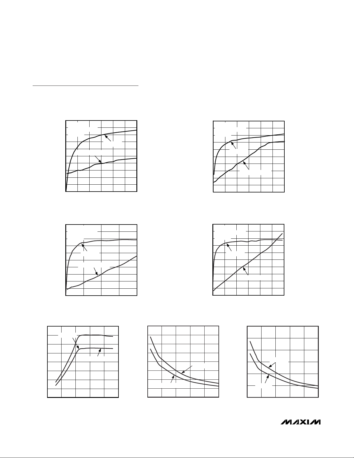
Page 9

Typical Operating Characteristics (continued)
(MAX9736A, V
PVDD
= 12V, MOD = high, spread-spectrum modulation mode, V
GND
= V
PGND
= 0V, V
SHDN
= V
MUTE
= 5V, unless
otherwise noted.)
MAX9736
Mono/Stereo High-Power Class D Amplifier
_______________________________________________________________________________________
9
TOTAL OUTPUT POWER
vs. LOAD RESISTANCE
40
35
30
25
20
15
TOTAL OUTPUT POWER (W)
10
5
0
TOTAL HARMONIC DISTORTION
PLUS NOISE vs. OUTPUT POWER
10
V
= 18V,
PVDD
SPREAD SPECTRUM,
8Ω LOAD
1
1kHz
0.1
THD+N (%)
0.01
V
= 24V,
PVDD
SPREAD SPECTRUM
10% THD+N
1% THD+N
LOAD RESISTANCE (Ω)
6kHz
POWER-SUPPLY REJECTION RATIO
0
100mV
-10
MAX9736 toc24
252015105030
MAX9736 toc08
20Hz
PVDD RIPPLE,
8Ω LOAD
-20
-30
-40
-50
PSRR (dB)
-60
-70
-80
-90
10 100k
0
8Ω LOAD,
SPREAD SPECTRUM
-20
-40
-60
-80
OUTPUT AMPLITUDE (dBV)
-100
vs. FREQUENCY
,
P-P
FREQUENCY (Hz)
INBAND OUTPUT SPECTRUM
10k1k100
MAX9736 toc25
CROSSTALK (dB)
-100
-120
MAX9736 toc28
OUTPUT AMPLITUDE (dBV)
-100
CROSSTALK vs. FREQUENCY
0
1W OUTPUT,
8Ω LOAD,
-20
SPREAD SPECTRUM
-40
-60
-80
RIGHT TO LEFT
FREQUENCY (Hz)
WIDEBAND OUTPUT SPECTRUM
20
0
-20
-40
-60
-80
LEFT TO RIGHT
10k1k10010 100k
8Ω LOAD,
FIXED FREQUENCY
MAX9736 toc26
MAX9736 toc29
MAX9736 toc30
-120
020
SHDN ON-/OFF-RESPONSE
0.001
020
OUTPUT POWER (W)
18161412108642
WIDEBAND OUTPUT SPECTRUM
10
0
-10
-20
-30
-40
-50
-60
-70
OUTPUT AMPLITUDE (dBV)
-80
-90
-100
FREQUENCY (MHz)
8Ω LOAD,
SPREAD SPECTRUM
1010.1 100
FREQUENCY (kHz)
40ms/div
15105
MAX9736 toc31
SHDN
2V/div
OUTPUT
5V/div
-120
0.1 100
FREQUENCY (MHz)
101
MUTE ON-/OFF-RESPONSE
40ms/div
MAX9736 toc32
MUTE
2V/div
OUTPUT
5V/div
Page 10

Typical Operating Characteristics (continued)
(MAX9736A, V
PVDD
= 12V, MOD = high, spread-spectrum modulation mode, V
GND
= V
PGND
= 0V, V
SHDN
= V
MUTE
= 5V, unless
otherwise noted.)
MAX9736
Mono/Stereo High-Power Class D Amplifier
10 ______________________________________________________________________________________
MAX9736 toc33
MAX9736 toc34
40
V
REGEN
30
20
SUPPLY CURRENT (mA)
10
SUPPLY CURRENT
vs. PVDD SUPPLY VOLTAGE
= V
= V
SHDN
= 3.3V
MUTE
20
15
10
SUPPLY CURRENT (mA)
vs. PVDD SUPPLY VOLTAGE
V
= 0V,
REGEN
= V
V
MUTE
SHDN
VS = 5V
5
SUPPLY CURRENT
= 3.3V,
SUPPLY CURRENT (mA)
SUPPLY CURRENT
vs. VS
15
V
= 0V,
REGEN
= V
V
MUTE
13
11
9
7
SHDN
SUPPLY VOLTAGE
= 3.3V
MAX9736 toc35
0
828
231813
SHUTDOWN CURRENT
vs. PVDD SUPPLY VOLTAGE
3
V
= V
REGEN
V
MUTE
2
1
0
SHUTDOWN CURRENT (μA)
-1
-2
828
= 0V,
SHDN
= 3.3V
SUPPLY VOLTAGE (V)
MAX9736 toc36
24201612
0
TOTAL HARMONIC DISTORTION
PLUS NOISE vs. FREQUENCY
1
V
= 12V,
PVDD
FIXED FREQUENCY,
4Ω LOAD, MONO
0.1
THD+N (%)
0.01
0.001
10 100k
FREQUENCY (Hz)
TOTAL HARMONIC DISTORTION
PLUS NOISE vs. OUTPUT POWER
10
V
= 12V,
PVDD
FIXED FREQUENCY,
4Ω LOAD, MONO
1
6kHz
THD+N (%)
0.1
0.01
020
1kHz
OUTPUT POWER (W)
20Hz
MAX9736 toc39
18161412108642
5
231813828
4.5 5.5
TOTAL HARMONIC DISTORTION
PLUS NOISE vs. FREQUENCY
1
V
= 12V,
P
= 10W
OUT
MAX9736 toc37
P
= 6W
OUT
10k1k100
PVDD
SPREAD SPECTRUM,
4Ω LOAD, MONO
P
0.1
THD+N (%)
0.01
0.001
10 100k
OUT
TOTAL HARMONIC DISTORTION PLUS NOISE
vs. OUTPUT POWER (V
= 12V,
DD
SPREAD SPECTRUM, 4Ω LOAD, MONO)
10
1
THD+N (%)
0.1
0.01
020
6kHz
1kHz
OUTPUT POWER (W)
VS VOLTAGE (V)
= 10W
FREQUENCY (Hz)
20Hz
18161412108642
P
OUT
MAX9736 toc40
5.35.14.94.7
MAX9736 toc38
= 6W
10k1k100
Page 11

TOTAL HARMONIC DISTORTION
PLUS NOISE vs. OUTPUT POWER
MAX9736 toc42
OUTPUT POWER (W)
THD+N (%)
30252015105
0.1
1
10
0.01
035
6kHz
1kHz
20Hz
V
PVDD
= 18V,
SPREAD SPECTRUM,
4Ω LOAD, MONO
TOTAL HARMONIC DISTORTION
PLUS NOISE vs. OUTPUT POWER
MAX9736 toc43
OUTPUT POWER (W)
THD+N (%)
30252015105
0.1
1
10
0.01
035
1kHz
V
PVDD
= 24V,
FIXED FREQUENCY,
4Ω LOAD, MONO
6kHz
20Hz
Typical Operating Characteristics (continued)
(MAX9736A, V
PVDD
= 12V, MOD = high, spread-spectrum modulation mode, V
GND
= V
PGND
= 0V, V
SHDN
= V
MUTE
= 5V, unless
otherwise noted.)
MAX9736
Mono/Stereo High-Power Class D Amplifier
______________________________________________________________________________________
11
TOTAL HARMONIC DISTORTION
PLUS NOISE vs. OUTPUT POWER
10
V
= 18V,
PVDD
FIXED FREQUENCY,
4Ω LOAD, MONO
1
6kHz
THD+N (%)
0.1
0.01
035
1kHz
OUTPUT POWER (W)
MAX9736 toc41
20Hz
30252015105
TOTAL HARMONIC DISTORTION PLUS NOISE
vs. OUTPUT POWER (V
= 24V,
DD
SPREAD SPECTRUM, 4Ω LOAD, MONO)
10
1
6kHz
THD+N (%)
0.1
0.01
1kHz
20Hz
302418126036
OUTPUT POWER (W)
EFFICIENCY
vs. OUTPUT POWER
100
90
80
70
60
50
40
EFFICIENCY (%)
30
20
10
0
V
PVDD
= 24V
V
= 12V
PVDD
V
= 18V
PVDD
4Ω LOAD, MONO,
f = 1kHz SPREAD SPECTRUM
OUTPUT POWER (W)
15105020
MAX9736 toc44
MAX9736 toc46
90
80
70
60
50
40
EFFICIENCY (%)
30
20
10
(LOAD = 4Ω, f = 1kHz, SPREAD SPECTRUM, MONO)
40
35
30
25
20
15
OUTPUT POWER (W)
10
5
0
EFFICIENCY
vs. OUTPUT POWER
MAX9736 toc45
V
= 12V
PVDD
V
= 18V
PVDD
V
= 24V
PVDD
4Ω LOAD, MONO,
0
020
OUTPUT POWER vs. V
10% THD+N
828
1kHz FIXED FREQUENCY
OUTPUT POWER (W)
4Ω LOAD
f = 1kHz,
SPREAD SPECTRUM, MONO
SUPPLY VOLTAGE (V)
15105
DD
MAX9736 toc47
1% THD+N
262410 12 14 18 2016 22
Page 12

Typical Operating Characteristics (continued)
(MAX9736A, V
PVDD
= 12V, MOD = high, spread-spectrum modulation mode, V
GND
= V
PGND
= 0V, V
SHDN
= V
MUTE
= 5V, unless
otherwise noted.)
MAX9736
Mono/Stereo High-Power Class D Amplifier
12 ______________________________________________________________________________________
20
18
16
14
12
10
8
OUTPUT POWER (W)
6
4
2
0
030
OUTPUT POWER
vs. LOAD RESISTANCE
V
= 12V, MONO,
PVDD
SPREAD SPECTRUM
10% THD+N
1% THD+N
LOAD RESISTANCE (Ω)
40
MAX9736 toc48
252015105
35
30
25
20
15
OUTPUT POWER (W)
10
5
0
030
OUTPUT POWER
vs. LOAD RESISTANCE
1% THD+N
LOAD RESISTANCE (Ω)
V
= 18V, MONO,
PVDD
SPREAD SPECTRUM
10% THD+N
25205 10 15
MAX9736 toc49
OUTPUT POWER
vs. LOAD RESISTANCE
40
35
30
25
20
15
OUTPUT POWER (W)
10
5
1% THD+N
0
030
LOAD RESISTANCE (Ω)
V
= 24V, MONO,
PVDD
SPREAD SPECTRUM
10% THD+N
25205 10 15
MAX9736 toc50
45
vs. PVDD SUPPLY VOLTAGE
V
= V
REGEN
30
15
SUPPLY CURRENT (mA)
0
8
13
SUPPLY CURRENT
= V
MUTE
SUPPLY VOLTAGE (V)
= 3.3V, MONO
SHDN
V
REGEN
V
MUTE
MONO
= 0V,
= V
SUPPLY CURRENT
vs. VS VOLTAGE
= 3.3V,
SHDN
VS VOLTAGE (V)
MAX9736 toc53
5.45.35.25.15.04.94.84.74.6
SUPPLY CURRENT
vs. PVDD SUPPLY VOLTAGE
20
V
= 0V,
REGEN
= V
V
MUTE
MAX9736 toc51
2318
28
VS = 5V, MONO
15
10
SUPPLY CURRENT (mA)
5
0
828
= 3.3V,
SHDN
SUPPLY VOLTAGE (V)
231813
20
MAX9736 toc52
15
10
SUPPLY CURRENT (mA)
5
0
4.5 5.5
Page 13
MAX9736
Mono/Stereo High-Power Class D Amplifier
______________________________________________________________________________________ 13
Pin Description
PIN NAME FUNCTION
1, 2 OUTL- Left-Channel Negative Speaker Output
3 BOOT Charge-Pump Output. Connect a 1μF charge-pump holding capacitor from BOOT to PVDD.
4 MONO Mono Select. Set MONO high for mono mode, low for stereo mode.
5 FBL Left-Channel Feedback. Connect feedback resistor between FBL and INL to set amplifier gain.
6 INL Stereo Left-Channel Inverting Input. In mono mode, INL is the inverting audio input for the mono amplifier.
7, 8, 17 N.C. No Connection. Not internally connected. OK to connect to PGND.
9 MUTE Mute Input. Drive MUTE low to place the device in mute mode.
10 SHDN Shutdown Input. Drive SHDN low to place the device in shutdown mode.
Internal Regulator Enable Input. Connect REGEN to SHDN
11 REGEN
12 COM Internal 2V Bias. Bypass COM to AGND with a 1μF capacitor.
13, 14 AGND Analog Ground
15 REG Internal Regulator Output. Bypass REG to AGND with a 1μF capacitor.
16 VS
18 INR
19 FBR Right-Channel Feedback. Connect feedback resistor between FBR and INR to set amplifier gain.
20 MOD
21 C1N Charge-Pump Flying-Capacitor Negative Terminal
22 C1P Charge-Pump Flying-Capacitor Positive Terminal
23, 24 OUTR- Right-Channel Negative Speaker Output
25, 26 OUTR+ Right-Channel Positive Speaker Output
27, 30 PVDD
28, 29 PGND Power Ground
31, 32 OUTL+ Left-Channel Positive Speaker Output
— EP Exposed Pad. Must be externally connected to PGND.
low to disable the internal regulator, and supply the device with an external 5V supply on VS. See the
Power-Supply Sequencing section.
5V Regulator Supply. Bypass VS to AGND with a 1μF capacitor. If REGEN is low, the internal regulator is
disabled, and an external 5V supply must be connected to VS. See the Power-Supply Sequencing
section.
Stereo Right-Channel Inverting Audio Input. In mono mode, INR is the inverting audio input for the
uncommitted preamplifier (see the Mono Configuration section for more details).
Output Modulation Select. Sets the output modulation scheme:
= Low, classic PWM/fixed-frequency mode
V
MOD
V
= High, filterless modulation/spread-spectrum mode
MOD
Power Supply. Bypass each PVDD pin to ground with 0.1μF capacitors. Also, use a single 220μF
capacitor between PVDD and PGND.
to enable the internal regulator. Drive REGEN
Page 14
MAX9736
Mono/Stereo High-Power Class D Amplifier
14 ______________________________________________________________________________________
Detailed Description
The MAX9736A/B/D filterless, stereo Class D audio
power amplifiers offer Class AB performance and Class
D efficiency with minimal board space. The MAX9736A
outputs 2x15W in stereo mode and 30W in mono mode.
The MAX9736B/D output 2x6W in stereo mode and 12W
in mono mode. These devices operate from an 8V to
28V supply range.
The MAX9736 features a filterless, spread-spectrum
switching mode (MOD = high) or a classic PWM fixedfrequency switching mode (MOD = low).
The MAX9736 features externally set gain and a lowpower shutdown mode that reduces supply current to
less than 1µA. Comprehensive click-and-pop circuitry
minimizes noise into and out of shutdown or mute.
Operating Modes
Filterless Modulation/PWM Modulation
The MAX9736 features two output modulation schemes,
filterless modulation (MOD = high) or classic PWM (MOD
= low). Maxim’s unique, filterless modulation scheme
eliminates the LC filter required by traditional Class D
amplifiers, reducing component count, conserving
board space, and reducing system cost. Configure for
classic PWM output when using a full LC filter.
Click-and-pop protection does not apply when the output is switching between modulation schemes. To
maintain click-and-pop protection when switching
between output schemes the device must enter shutdown mode and be configured to the new output
scheme before the startup sequence is finished.
Spread-Spectrum Mode
The MAX9736 features a unique spread-spectrum mode
that flattens the wideband spectral components, improving EMI radiated by the speaker and cables. The
switching frequency of the Class D amplifier varies randomly by ±6kHz around the 300kHz center frequency.
Instead of a large amount of spectral energy present at
multiples of the switching frequency, the energy is
spread over a bandwidth that increases with frequency.
Above a few megahertz, the wideband spectrum looks
like white noise for EMI purposes. A proprietary amplifier
topology ensures this white noise does not corrupt the
noise floor in the audio bandwidth. The spread-spectrum mode is enabled only with filterless modulation.
Efficiency
The high efficiency of a Class D amplifier is due to the
switching operation of the output stage transistors. In a
Class D amplifier, the output transistors act as switches
and consume negligible power. Power loss associated
with the Class D output stage is due to the I2R loss of
the MOSFET on-resistance, various switching losses,
and quiescent current overhead.
The theoretical best efficiency of a linear amplifier is 78%
at peak output power. Under typical music reproduction
levels, the efficiency falls below 30%, whereas the
MAX9736 exhibits > 80% efficiency under the same conditions (Figure 1).
Shutdown
The MAX9736 features a shutdown mode that reduces
power consumption and extends battery life in portable
applications. The shutdown mode reduces supply current to 1µA (typ). Drive SHDN high for normal operation. Drive SHDN low to place the device in low-power
shutdown mode. In shutdown mode, the outputs are
high impedance; and the common-mode voltage at the
output decays to zero. In shutdown mode, connect
REGEN low to minimize current consumption.
Mute Function
The MAX9736 features a clickless-and-popless mute
mode. When the device is muted, the signal is attenuated at the speaker and the outputs stop switching. To
mute the MAX9736, drive MUTE low. Hold MUTE low
during system power-up and power-down to ensure
that clicks and pops caused by circuits before the
MAX9736 are suppressed.
EFFICIENCY
vs. TOTAL OUTPUT POWER
MAX9736 fig01
TOTAL OUTPUT POWER (W)
EFFICIENCY (%)
15105
10
20
30
40
50
60
70
80
90
100
0
020
MAX9736A
CLASS AB
Figure 1. MAX9736A Efficiency vs. Class AB Efficiency
Page 15

MAX9736
Mono/Stereo High-Power Class D Amplifier
______________________________________________________________________________________ 15
Click-and-Pop Suppression
The MAX9736 features comprehensive click-and-pop
suppression that minimizes audible transients on startup and shutdown. While in shutdown, the H-bridge is in
a high-impedance state.
Mono Configuration
The MAX9736 features a mono mode that allows the
right and left channels to operate in parallel, achieving
up to 30W (MAX9736A) of output power. Apply a logichigh to MONO to enable mono mode. In mono mode,
an audio signal applied to the left channel (INL) is routed to the H-bridges of both channels. Also in mono
mode, the right-channel preamplifier becomes an
uncommitted operational amplifier, allowing for flexibility in system design. Connect OUTL+ to OUTR+ and
OUTL- to OUTR- using heavy PCB traces as close as
possible to the device. Driving MONO low (stereo
mode) while the outputs are wired together in mono
mode can trigger the short-circuit or thermal-overload
protection or both.
Current Limit
When the output current reaches the current limit, 4.6A
(typ), the MAX9736 disables the outputs and initiates a
450μs startup sequence. The shutdown and startup
sequence is repeated until the output fault is removed.
Properly designed applications do not enter currentlimit mode unless the output is short circuited or connected incorrectly.
Thermal Shutdown
When the die temperature reaches the thermal shutdown threshold, +160°C (typ), the MAX9736 outputs
are disabled. When the die temperature decreases by
30°C, normal operation resumes. Some causes of thermal shutdown are excessively low load impedance,
poor thermal contact between the MAX9736‘s exposed
pad and the PCB, elevated ambient temperature, or
poor PCB layout and assembly.
Applications Information
Filterless Class D Operation
The MAX9736 meets EN55022B EMC radiation limits
with an inexpensive ferrite bead and capacitor filter
when the speaker leads are less than or equal to 1m.
Select a ferrite bead with 100Ω to 600Ω impedance
and rated for at least 2A. The capacitor value varies
based on the ferrite bead chosen and the speaker lead
length. See Figure 3 for the correct connections of
these components.
When evaluating the MAX9736 with a ferrite bead filter
and resistive load, include a series inductor (68μH for
8Ω load and 33μH for 4Ω load) to model the actual
loudspeaker’s behavior. Omitting the series inductor
Figure 3. Ferrite Bead Filter
Figure 2. EMI Performance
Figure 4. Output Filter for PWM Mode
40
35
30
25
20
AMPLITUDE (dBμV/m)
15
10
5
30 500 600 700
MAX9736
FB1 AND FB2 = WURTH 742792040
EN55022B LIMIT
400300200100
FREQUENCY (MHz)
FB1
FB2
C1
330pF
800
900 1000
C2
330pF
L1
MAX9736
L2
C2
C1
C3
C4
R1
C5
R2
Page 16

MAX9736
Mono/Stereo High-Power Class D Amplifier
16 ______________________________________________________________________________________
reduces the efficiency, the THD+N performance, and
the output power of the MAX9736. When evaluating
with a load speaker, no series inductor is required.
Inductor-Based Output Filters
Some applications use the MAX9736 with a full inductor-/capacitor-based (LC) output filter. Select the PWM
output mode for best audio performance. See Figure 4
for the correct connections of these components.
The load impedance of the speaker determines the filter component selection (see Table 1).
Inductors L1 and L2, and capacitor C1 form the primary output filter. Capacitors C2 and C3 provide commonmode filtering to reduce radiated emissions. Capacitors
C4 and C5, plus resistors R1 and R2, form a Zobel at
the output. A Zobel corrects the output loading to compensate for the rising impedance of the loudspeaker.
Without a Zobel the filter exhibits a peak response near
the cutoff frequency.
Component Selection
Gain-Setting Resistors
External feedback resistors set the gain of the
MAX9736. The output stage provides a fixed internal
gain in addition to the externally set input stage gain.
For the MAX9736A/D, the fixed output-stage gain is set
at 17dB (7V/V). For the MAX9736B, the fixed outputstage gain is set at 13.6dB (4.8V/V). Set overall gain by
using resistors R
F
and RIN(Figure 5)as follows:
where A
V
is the desired voltage gain. Choose R
F
between 10kΩ and 50kΩ.
The FB terminal is an op amp output and the IN terminal is the op amp inverting input, allowing the MAX9736
to be configured as a summing amplifier, a filter, or an
equalizer.
Input Capacitor
An input capacitor, CIN, in conjunction with the input
resistor, R
IN
, of the MAX9736 forms a highpass filter
that removes the DC bias from an incoming signal. The
AC-coupling capacitor allows the amplifier to automatically bias the signal to an optimum DC level. Assuming
zero-source impedance, the -3dB point of the highpass
filter is given by:
Choose CINso that f
-3dB
is well below the lowest frequency of interest. Use capacitors whose dielectrics have low
voltage coefficients. Capacitors with high-voltage coefficients cause increased distortion close to f
-3dB
.
COM Capacitor
COM is the output of the internally generated DC bias
voltage. Bypass COM with a 1μF capacitor to AGND.
Power Supplies
The MAX9736 features separate supplies for signal and
power portions of the device, allowing for the optimum
combination of headroom, power dissipation, and noise
immunity. The speaker amplifiers are powered from
PVDD and can range from 8V to 28V. The remainder of
the MAX9736 is powered by VS.
Power-Supply Sequencing
During power-up and power-down, VS must not exceed
PVDD. VS greater than PVDD will damage the device.
Table 1. Suggested Values for LC Filter
Figure 5. Setting Gain
RL (Ω) L1, L2 (µH) C1 (µF) C2, C3 (µF) C4, C5 (µF) R1, R2 (Ω)
4 10 0.47 0.10 0.22 10
8 15 0.15 0.15 0.15 15
16 33 0.10 0.10 0.10 33
⎛
⎞
R
MAX A D A
9736 7 1
MAX B
9736
:.
:
V
V
=
=
.A
−48
F
−
⎛
R
⎜
R
⎝
VV
⎜
⎟
R
⎝
⎠
IN
⎞
F
VV
⎟
⎠
IN
=
2π
1
RC
IN IN
f
dB
−
3
R
F
C
IN
R
AUDIO
INPUT
IN
C
COM
FB_
IN_
COM
MAX9736
OUT_+
OUT_-
Page 17

MAX9736
Mono/Stereo High-Power Class D Amplifier
______________________________________________________________________________________ 17
Internal Regulator
The MAX9736 features an internal 5V regulator, VS,
powered from PVDD. Connect REGEN to SHDN so that
the internal 5V regulator is enabled/disabled when the
MAX9736 is enabled/disabled. If an external 5V supply
is available, drive REGEN low and connect external 5V
supply to VS to minimize the power dissipation of the
MAX9736.
Supply Bypassing,
Layout, and Grounding
Proper layout and grounding are essential for optimum
performance. Use wide traces for the power-supply
inputs and amplifier outputs to minimize losses due to
parasitic trace resistance. Proper grounding improves
audio performance, minimizes crosstalk between channels, and prevents switching noise from coupling into
the audio signal. Connect PGND and AGND together at
a single point on the PCB. Route all traces that carry
switching transients away from AGND and the
traces/components in the audio signal path.
Bypass each PVDD pin with a 0.1μF capacitor to PGND.
Place the bypass capacitors as close as possible to the
MAX9736. Place a 220μF capacitor between PVDD and
PGND. Bypass VS with a 1μF capacitor to AGND.
Use wide, low-resistance output traces. Current drawn
from the outputs increases as load impedance
decreases. High-output trace resistance decreases the
power delivered to the load. The MAX9736 TQFN package features an exposed thermal paddle on its underside. This paddle lowers the package’s thermal
resistance by providing a heat conduction path from
the die to the PCB. Connect the exposed thermal pad
to PGND by using a large pad and multiple vias to the
PGND plane.
Page 18

MAX9736
Mono/Stereo High-Power Class D Amplifier
18 ______________________________________________________________________________________
Typical Application Circuit for Stereo Output Configuration
8V TO 28V
C
0.1μF
0.1μF
BULK
220μF
20k
470nF
20k
470nF
C1
1μF
VS
PVDD
16
REG
15
1μF
Ω
20k
Ω
Ω
Ω
20k
FBL 5
INL 6
COM 12
1μF
INR 18
FBR 19
REGULATOR
27, 30 2122
BIAS
0.1μF
C1P
CHARGE PUMP
POWER
STAGE
C1N
3 BOOT
31, 32 OUTL+
1, 2 OUTL-
25, 26 OUTR+
23, 24 OUTR-
C2
1μF
(16V)
11
REGEN
10
SHUTDOWN
MUTE
NOTE: PREAMPLIFIER GAIN SET AT 0dB.
SHDN
9
MUTE
5V
MOD
20
MONO
4
CONTROL
13, 14
AGND
MAX9736
28, 29
PGND
7, 8, 17
N.C.
Page 19

MAX9736
Mono/Stereo High-Power Class D Amplifier
______________________________________________________________________________________ 19
Typical Application Circuit for Single (Mono) Output Configuration
8V TO 28V
C
0.1μF
C1P
CHARGE PUMP
BULK
220μF
C1
C1N
3 BOOT
31, 32 OUTL+
1, 2 OUTL-
LPF
FBR
1μF
REG
FBL 5
INL 6
0.1μF
1μF
VS
PVDD
27, 30 2122
16
15
REGULATOR
0.1μF
C2
1μF
(16V)
HPF
AUDIO
INPUT
SHUTDOWN
MUTE
FBR
1μF
5V
COM 12
INR 18
FBR 19
REGEN
SHDN
MUTE
MOD
MONO
11
10
9
20
4
CONTROL
BIAS
13, 14
AGND
POWER
STAGE
MAX9736
28, 29
PGND
25, 26 OUTR+
23, 24 OUTR-
7, 8, 17
N.C.
Page 20

MAX9736
Mono/Stereo High-Power Class D Amplifier
20 ______________________________________________________________________________________
Chip Information
PROCESS: BiCMOS
Pin Configuration
MAX9736
TQFN
TOP VIEW
29
30
28
27
12
11
13
OUTL-
MONO
FBL
INL
N.C.
14
OUTL-
OUTR-
C1N
MOD
OUTR-
FBR
INR
12
PGND
4567
2324 22 20 19 18
PGND
PVDD
AGND
AGND
COM
REGEN
BOOT
C1P
3
21
31
10
OUTL+
SHDN
32
9
OUTL+
MUTE
EP*
+
EP* = EXPOSED PAD, CONNECT TO PGND.
PVDD
26
15
REG
OUTR+
25
16
VS
N.C.
N.C.
8
17
OUTR+
Ordering Information (continued)
PART
STEREO/MONO
PIN-PACKAGE
MAX9736AETJ/V+
2 x 15W/
1 x 30W
32 TQFN-EP*
7mm x 7mm
MAX9736BETJ+
2 x 6W/
1 x 12W
32 TQFN-EP*
7mm x 7mm
MAX9736BETJ/V+
2 x 6W/
1 x 12W
32 TQFN-EP*
7mm x 7mm
MAX9736DETJ+
2 x 6W/
1 x 12W
32 TQFN-EP*
5mm x 5mm
MAX9736DETJ/V+
2 x 6W/
1 x 12W
32 TQFN-EP*
5mm x 5mm
Note: All devices are specified over the -40°C to +85°C operating temperature range.
+
Denotes a lead(Pb)-free/RoHS-compliant package.
*
EP = Exposed pad.
/V denotes an automotive qualified part.
OUTPUT POWER
Page 21

MAX9736
Mono/Stereo High-Power Class D Amplifier
______________________________________________________________________________________ 21
Package Information
For the latest package outline information and land patterns, go to www.maxim-ic.com/packages.
PACKAGE TYPE PACKAGE CODE DOCUMENT NO.
32 TQFN-EP (7mm x 7mm) T3277-3
21-0144
32 TQFN-EP (5mm x 5mm) T3255-4
21-0140
Page 22

MAX9736
Mono/Stereo High-Power Class D Amplifier
22 ______________________________________________________________________________________
Package Information (continued)
For the latest package outline information and land patterns, go to www.maxim-ic.com/packages.
Page 23

MAX9736
Mono/Stereo High-Power Class D Amplifier
______________________________________________________________________________________ 23
Package Information (continued)
For the latest package outline information and land patterns, go to www.maxim-ic.com/packages.
QFN THIN.EPS
Page 24

MAX9736
Mono/Stereo High-Power Class D Amplifier
24 ______________________________________________________________________________________
Package Information (continued)
For the latest package outline information and land patterns, go to www.maxim-ic.com/packages.
Page 25

MAX9736
Mono/Stereo High-Power Class D Amplifier
Maxim cannot assume responsibility for use of any circuitry other than circuitry entirely embodied in a Maxim product. No circuit patent licenses are
implied. Maxim reserves the right to change the circuitry and specifications without notice at any time.
Maxim Integrated Products, 120 San Gabriel Drive, Sunnyvale, CA 94086 408-737-7600 ____________________
25
© 2009 Maxim Integrated Products Maxim is a registered trademark of Maxim Integrated Products, Inc.
Revision History
REVISION
NUMBER
0 1/08 Initial release —
1 12/08 Corrected various errors 1–15, 17–21
2 8/09
3 9/09
REVISION
DATE
DESCRIPTION
Added MAX9736D and automotive parts numbers and updated the Absolute
Maximum Ratings section
Corrected error in Absolute Maximum Ratings, Pin Description, Typical
Application Circuit for Stereo Output Configuration, and Typical Application
Circuit for Single (Mono) Output Configuration
1, 2, 3, 4,13,
15, 19, 20, 21
2, 12, 17, 18
PAGES
CHANGED
 Loading...