

Page 1
General Description
The MAX9723 stereo DirectDrive®headphone amplifier
with BassMax and volume control is ideal for portable
audio applications where space is at a premium and performance is essential. The MAX9723 operates from a single 1.8V to 3.6V power supply and includes features that
reduce external component count, system cost, board
space, and improves audio reproduction.
The headphone amplifier uses Maxim’s patented
DirectDrive architecture that produces a ground-referenced output from a single supply, eliminating the need
for large DC-blocking capacitors. The headphone amplifiers deliver 62mW into a 16Ω load, feature low 0.006%
THD+N, and high 90dB PSRR. The MAX9723 features
Maxim’s industry-leading click-and-pop suppression.
The BassMax feature boosts the bass response of the
amplifier, improving audio reproduction when using
inexpensive headphones. The integrated volume control features 32 discrete volume levels, eliminating the
need for an external potentiometer. BassMax and the
volume control are enabled through the I2C/SMBus™compatible interface. Shutdown is controlled through
either the hardware or software interfaces.
The MAX9723 consumes only 3.7mA of supply current
at 1.8V, provides short-circuit and thermal-overload
protection, and is fully specified over the extended
-40°C to +85°C temperature range. The MAX9723 is
available in a tiny (2mm x 2mm x 0.62mm) 16-bump
chip-scale package (UCSP™) or 16-pin thin QFN (4mm
x 4mm x 0.8mm) package.
Applications
Features
♦ 62mW, DirectDrive Headphone Amplifier
Eliminates Bulky DC-Blocking Capacitors
♦ 1.8V to 3.6V Single-Supply Operation
♦ Integrated 32-Level Volume Control
♦ High 90dB PSRR at 1kHz
♦ Low 0.006% THD+N
♦ Industry-Leading Click-and-Pop Suppression
♦ ±8kV HBM ESD-Protected Headphone Outputs
♦ Short-Circuit and Thermal-Overload Protection
♦ Low-Power Shutdown Mode (5µA)
♦ Software-Enabled Bass Boost (BassMax)
♦ I2C/SMBus-Compatible Interface
♦ Available in Space-Saving, Thermally Efficient
Packages:
16-Bump UCSP (2mm x 2mm x 0.62mm)
16-Pin Thin QFN (4mm x 4mm x 0.8mm)
MAX9723
Stereo DirectDrive Headphone Amplifier
with BassMax, Volume Control, and I2C
________________________________________________________________ Maxim Integrated Products 1
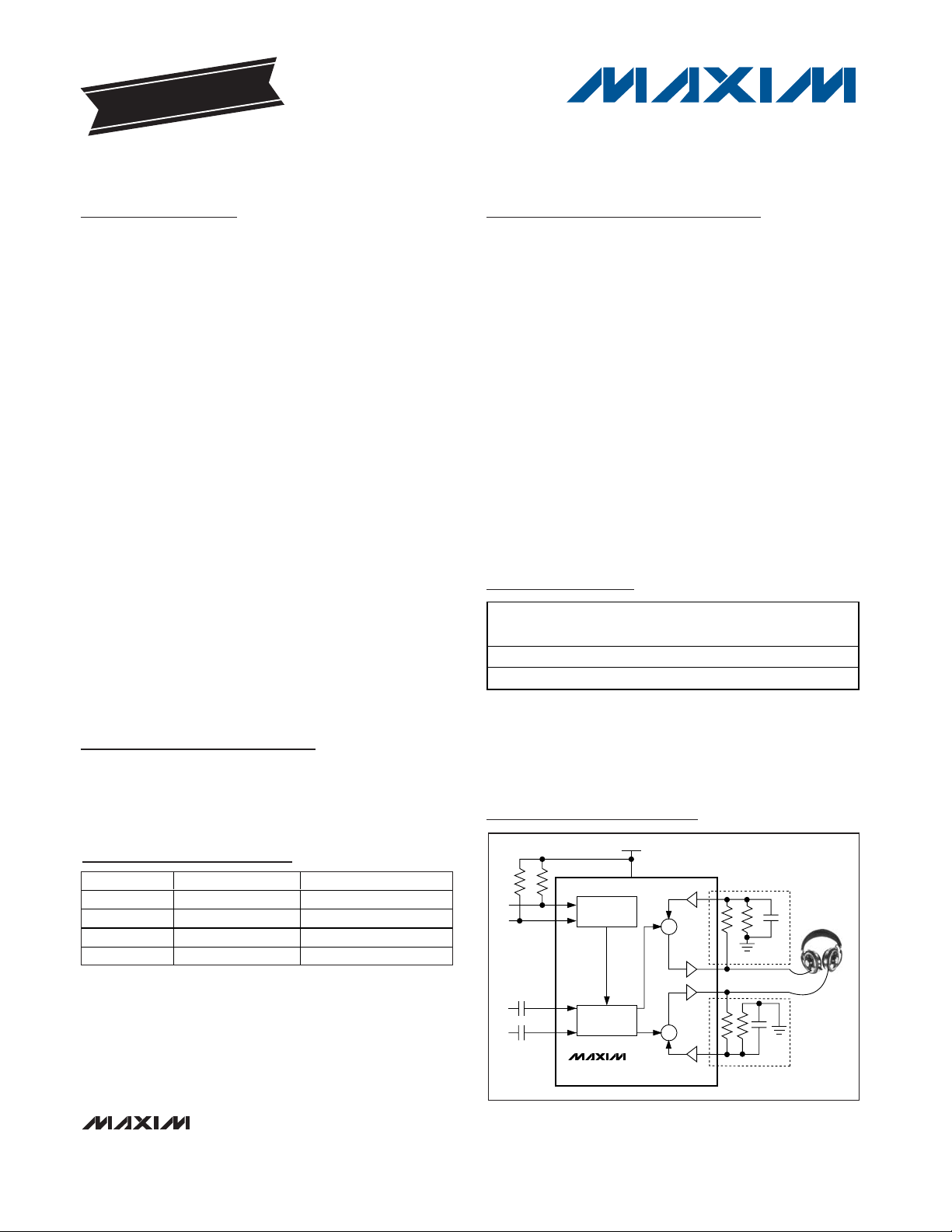
I2C INTERFACE
VOLUME
CONTROL
BassMax
BassMax
1.8V TO 3.6V SUPPLY
SCL
BBL
OUTL
BBR
OUTR
SDA
INL
INR
MAX9723
Σ
Σ
Block Diagram
Ordering Information
19-3509; Rev 2; 8/08
EVALUATION KIT
AVAILABLE
PART**
PINPACKAGE
PKG
CODE
MAX9723_EBE-T*
B16-1
MAX9723_ETE+
16 TQFN
T1644-4
DirectDrive is a registered trademark of Maxim Integrated
Products, Inc.
SMBus is a trademark of Intel Corp.
UCSP is a trademark of Maxim Integrated Products, Inc.
**Replace the ‘_’ with the one-letter code that denotes the
slave address and maximum programmable gain. See the
Selector Guide.
+Denotes a lead-free/RoHS-compliant package.
*Future product—contact factory for availability.
Pin Configurations appear at end of data sheet.
PDA Audio
Portable CD Players
Mini Disc Players
Automotive Multimedia
MP3-Enabled Cellular
Phones
MP3 Players
PART
SLAVE ADDRESS
MAXIMUM GAIN (dB)
MAX9723A
1001100 0
MAX9723B
1001101 0
MAX9723C
1001100 +6
MAX9723D
1001101 +6
Selector Guide
For pricing, delivery, and ordering information, please contact Maxim Direct at 1-888-629-4642,
or visit Maxim's website at www.maxim-ic.com.
TEMP RANGE
-40°C to +85°C
-40°C to +85°C
16 UCSP-16
Page 2
MAX9723
Stereo DirectDrive Headphone Amplifier
with BassMax, Volume Control, and I2C
2 _______________________________________________________________________________________
ABSOLUTE MAXIMUM RATINGS
Stresses beyond those listed under “Absolute Maximum Ratings” may cause permanent damage to the device. These are stress ratings only, and functional
operation of the device at these or any other conditions beyond those indicated in the operational sections of the specifications is not implied. Exposure to
absolute maximum rating conditions for extended periods may affect device reliability.
SGND to PGND .....................................................-0.3V to +0.3V
V
DD
to PGND............................................................-0.3V to +4V
PV
SS
to SVSS.........................................................-0.3V to +0.3V
C1P to PGND..............................................-0.3V to (V
DD
+ 0.3V)
C1N to PGND............................................(PV
SS
- 0.3V) to +0.3V
PV
SS
, SVSSto PGND ................................................+0.3V to -4V
IN_ to SGND ..................................(SV
SS
- 0.3V) to (VDD+ 0.3V)
SDA, SCL to PGND ..................................................-0.3V to +4V
SHDN to PGND ..........................................-0.3V to (VDD+ 0.3V)
OUT_ to SGND ............................................................-3V to +3V
BB_ to SGND...............................................................-2V to +2V
Duration of OUT_ Short Circuit to _GND ....................Continuous
Continuous Current Into/Out of:
V
DD
, C1P, PGND, C1N, PVSS, SVSS, or OUT_ ..............±0.85A
Any Other Pin.................................................................±20mA
Continuous Power Dissipation (T
A
= +70°C)
4 x 4 UCSP (derate 8.2mW/°C above +70°C) ...........659.2mW
16-Pin Thin QFN (derate 16.9mW/°C above +70°C) ....1349mW
Operating Temperature Range ...........................-40°C to +85°C
Junction Temperature......................................................+150°C
Storage Temperature Range .............................-65°C to +150°C
Bump Temperature (soldering)
Reflow ...........................................................................+230°C
Lead Temperature (soldering, 10s) .................................+300°C
ELECTRICAL CHARACTERISTICS
(VDD= SHDN = 3V, PGND = SGND = 0V, C1 = C2 = 1µF, BB_ = 0V. gain = 0dB, maximum volume, BassMax disabled. Load connect-
ed between OUT_ and SGND where specified. T
A
= T
MIN
to T
MAX
, unless otherwise noted. Typical values are at TA= +25°C.) (Note 1)
PARAMETER
CONDITIONS
UNITS
GENERAL
Supply Voltage Range V
DD
1.8 3.6 V
Quiescent Supply Current I
DD
No load 4 6.5 mA
Shutdown Supply Current
V
SHDN
= 0V 5 8.5 µA
Turn-On Time t
ON
µs
Turn-Off Time t
OFF
35 µs
Thermal Shutdown Threshold T
THRES
°C
Thermal Shutdown Hysteresis T
HYST
12 °C
HEADPHONE AMPLIFIER
Gain = 0dB,
MAX9723A/
MAX9723B
Output Offset Voltage V
OS
M easur ed b etw een
OU T_ and S GN D
( N ote 2)
Gain = +6dB,
MAX9723C/
MAX9723D
±5
mV
Input Resistance R
IN
All volume levels 10 17 27 kΩ
BBR, BBL Input Bias Current
nA
DC, VDD = 1.8V to 3.6V 73 90
f = 217Hz, 100mV
P-P
ripple,
V
DD
= 3.0V
87
f = 1kHz, 100mV
P-P
ripple,
V
DD
= 3.0V
86
Power-Supply Rejection Ratio PSRR (Note 2)
f = 20kHz, 100mV
P-P
ripple,
V
DD
= 3.0V
61
dB
SYMBOL
MIN TYP MAX
I
DD_SHDN
200
I
BIAS_BB
+143
±0.7 ±4.5
±0.8
±10 ±100
Page 3
MAX9723
Stereo DirectDrive Headphone Amplifier
with BassMax, Volume Control, and I2C
_______________________________________________________________________________________ 3
ELECTRICAL CHARACTERISTICS (continued)
(VDD= SHDN = 3V, PGND = SGND = 0V, C1 = C2 = 1µF, BB_ = 0V. gain = 0dB, maximum volume, BassMax disabled. Load connect-
ed between OUT_ and SGND where specified. T
A
= T
MIN
to T
MAX
, unless otherwise noted. Typical values are at TA= +25°C.) (Note 1)
PARAMETER
CONDITIONS
UNITS
RL = 32Ω 59
Output Power P
OUT
THD+N = 1%,
f
IN
= 1kHz
R
L
= 16Ω (Note 5) 38 60
mW
RL = 16Ω, P
OUT
= 35mW, fIN = 1kHz
Total Harmonic Distortion Plus
Noise
RL = 32Ω, P
OUT
= 45mW, fIN = 1kHz
%
Gain range bit 5 = 1 0
MAX9723A/
MAX9723B
Gain range bit 5 = 0 -5
dB
Gain range bit 5 = 1 +6
Maximum Gain A
MAX
MAX9723C/
MAX9723D
Gain range bit 5 = 0 +1
dB
BW = 22Hz to 22kHz 99
Signal-to-Noise Ratio SNR
R
L
= 32Ω,
V
OUT
= 1V
RMS A-weighted
dB
Slew Rate SR
V/µs
Capacitive Drive No sustained oscillations
pF
Output Resistance in Shutdown
V
SHDN
= 0V, measured from OUT_ to
SGND
20 kΩ
Output Capacitance in Shutdown
V
SHDN
= 0V, measured from OUT_ to
SGND
60 pF
Into
shutdown
-69
MAX9723A/
MAX9723B
Out of
shutdown
-71
Into
shutdown
-70
Click/Pop Level K
CP
RL = 32Ω,
peak voltage,
A-weighted,
32 samples
per second
(Notes 2, 4)
MAX9723C/
MAX9723D
Out of
shutdown
-69
dB
Charge-Pump Switching
Frequency
f
CP
700 kHz
Crosstalk XTALK
L to R or R to L, f = 10kHz,
V
OUT
= 1V
P-P
, RL = 32Ω, both channels
loaded
80 dB
DIGITAL INPUTS (SHDN, SDA, SCL)
Input High Voltage V
IH
0.7 x
V
Input Low Voltage V
IL
0.3 x
V
Input Leakage Current ±1µA
DIGITAL OUTPUTS (SDA)
Output Low Voltage V
OL
IOL = 3mA 0.4 V
Output High Current I
OH
V
SDA
= V
DD
1µA
SYMBOL
R
OUT_SHDN
C
OUT_SHDN
THD+N
MIN TYP MAX
0.006
0.004
100
0.35
300
505 600
V
DD
V
DD
Page 4
MAX9723
Stereo DirectDrive Headphone Amplifier
with BassMax, Volume Control, and I2C
4 _______________________________________________________________________________________
TIMING CHARACTERISTICS
(VDD= SHDN = 3V, PGND = SGND = 0V, C1 = C2 = 1µF, BB_ = 0V, gain = 0dB, maximum volume, BassMax disabled. Load connect-
ed between OUT_ and SGND where specified. T
A
= T
MIN
to T
MAX
, unless otherwise noted. Typical values are at TA= +25°C, see
Timing Diagram.) (Notes 1, 3)
PARAMETER
CONDITIONS
UNITS
Serial Clock Frequency f
SCL
0
kHz
Bus Free Time Between a STOP
and a START Condition
t
BUF
1.3 µs
START Condition Hold Time
0.6 µs
Low Period of the SCL Clock t
LOW
1.3 µs
High Period of the SCL Clock t
HIGH
0.6 µs
Setup Time for a Repeated
START Condition
t
SU:STA
0.6 µs
Data Hold Time
0 0.9 µs
Data Setup Time
ns
Maximum Rise Time of SDA and
SCL Signals
t
r
ns
Maximum Fall Time of SDA and
SCL Signals
t
f
ns
Setup Time for STOP Condition
0.6 µs
Pulse Width of Suppressed Spike
t
SP
ns
Maximum Capacitive Load for
Each Bus Line
pF
Note 1: All specifications are 100% tested at TA= +25°C. Temperature limits are guaranteed by design.
Note 2: Inputs AC-coupled to SGND.
Note 3: Guaranteed by design.
Note 4: Headphone mode testing performed with a 32Ω resistive load connected to GND. Mode transitions are controlled by
SHDN. The K
CP
level is calculated as: 20 x log [(level peak voltage during mode transition, no input signal)/(peak voltage
under normal operation at rated power)]. Units are expressed in dB.
Note 5: Output power MIN is specified at T
A
= +25°C.
SYMBOL
MIN TYP MAX
400
t
HD:STA
t
HD:DAT
t
SU:DAT
t
SU:STO
C
L_BUS
100
300
300
100
400
Page 5
MAX9723
Stereo DirectDrive Headphone Amplifier
with BassMax, Volume Control, and I2C
_______________________________________________________________________________________ 5
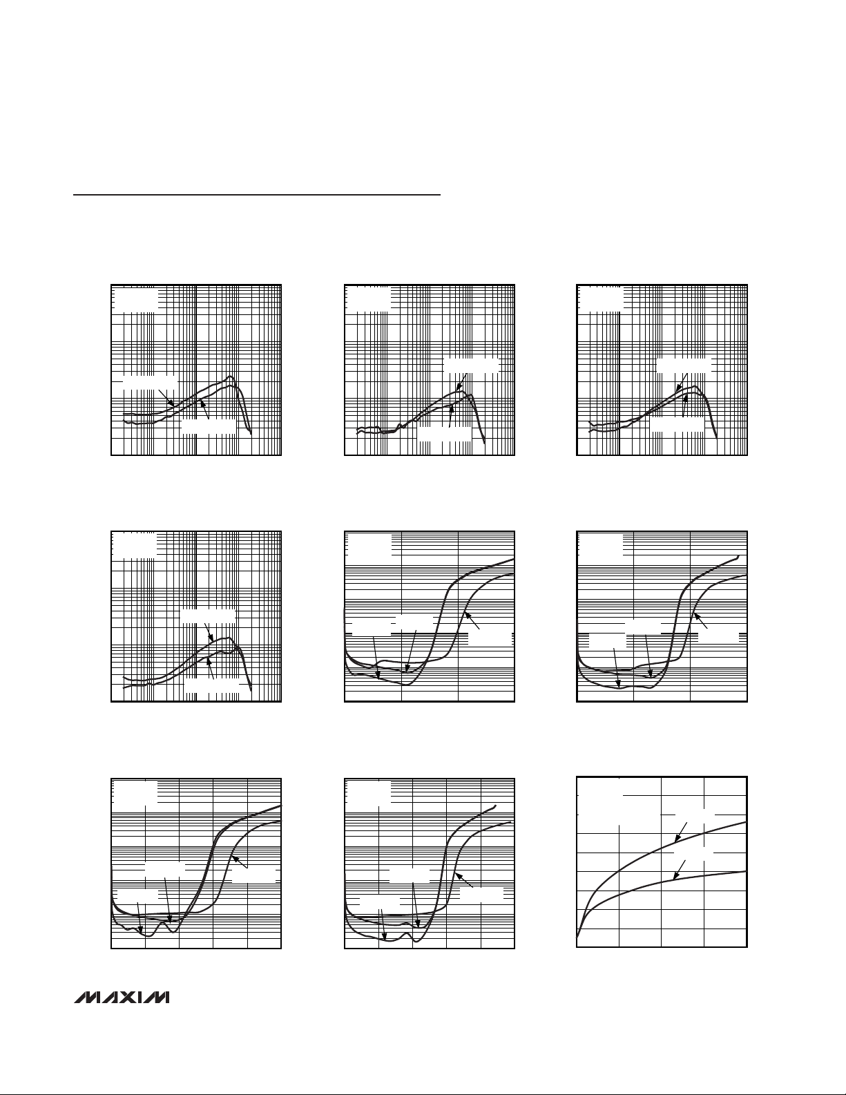
TOTAL HARMONIC DISTORTION PLUS
NOISE vs. FREQUENCY
MAX9723 toc01
FREQUENCY (Hz)
THD+N (%)
10k1k100
0.01
0.1
1
0.001
10 100k
VDD = 2.4V
R
L
= 16
Ω
P
OUT
= 10mW
P
OUT
= 25mW
TOTAL HARMONIC DISTORTION PLUS
NOISE vs. FREQUENCY
MAX9723 toc02
FREQUENCY (Hz)
THD+N (%)
10k1k100
0.01
0.1
1
0.001
10 100k
VDD = 2.4V
R
L
= 32
Ω
P
OUT
= 23mW
P
OUT
= 10mW
TOTAL HARMONIC DISTORTION PLUS
NOISE vs. FREQUENCY
MAX9723 toc03
FREQUENCY (Hz)
THD+N (%)
10k1k100
0.01
0.1
1
0.001
10 100k
VDD = 3V
R
L
= 16
Ω
P
OUT
= 37mW
P
OUT
= 20mW
TOTAL HARMONIC DISTORTION PLUS
NOISE vs. FREQUENCY
MAX9723 toc04
FREQUENCY (Hz)
THD+N (%)
10k1k100
0.01
0.1
1
0.001
10 100k
VDD = 3V
R
L
= 32
Ω
P
OUT
= 30mW
P
OUT
= 10mW
TOTAL HARMONIC DISTORTION PLUS
NOISE vs. OUTPUT POWER
MAX9723 toc05
OUTPUT POWER (mW)
THD+N (%)
4020
0.01
0.1
1
10
100
0.001
060
VDD = 2.4V
R
L
= 16
Ω
fIN = 1kHz
fIN = 20Hz
fIN = 10kHz
TOTAL HARMONIC DISTORTION PLUS
NOISE vs. OUTPUT POWER
MAX9723 toc06
OUTPUT POWER (mW)
THD+N (%)
4020
0.01
0.1
1
10
100
0.001
060
VDD = 2.4V
R
L
= 32
Ω
fIN = 1kHz
fIN = 10kHz
fIN = 20Hz
TOTAL HARMONIC DISTORTION PLUS
NOISE vs. OUTPUT POWER
MAX9723 toc07
OUTPUT POWER (mW)
THD+N (%)
80604020
0.01
0.1
1
10
100
0.001
0 100
VDD = 3V
R
L
= 16
Ω
fIN = 10kHz
fIN = 1kHz
fIN = 20Hz
TOTAL HARMONIC DISTORTION PLUS
NOISE vs. OUTPUT POWER
MAX9723 toc08
OUTPUT POWER (mW)
THD+N (%)
80604020
0.01
0.1
1
10
100
0.001
0100
VDD = 3V
R
L
= 32
Ω
fIN = 10kHz
fIN = 1kHz
fIN = 20Hz
0
40
60
80
100
120
140
160
180
0 20406080
POWER DISSIPATION
vs. OUTPUT POWER
MAX9723 toc09
OUTPUT POWER (mW)
POWER DISSIPATION (mW)
20
VDD = 2.4V
f
IN
= 1kHz
P
OUT
= P
OUTL
+ P
OUTR
OUTPUTS IN PHASE
RL = 32Ω
RL = 16Ω
Typical Operating Characteristics
(VDD= SHDN = 3V, PGND = SGND = 0V, C1 = C2 = 1µF, BB_ = 0V, gain = 0dB, maximum volume, BassMax disabled. Load connected between OUT_ and SGND where specified. Outputs in phase, both channels loaded. T
A
= +25°C, unless otherwise noted.)
(See Functional Diagram/Typical Operating Circuit)
Page 6
MAX9723
Stereo DirectDrive Headphone Amplifier
with BassMax, Volume Control, and I2C
6 _______________________________________________________________________________________
0
100
50
200
150
250
300
0406020 80 100 120
POWER DISSIPATION
vs. OUTPUT POWER
MAX9723 toc10
OUTPUT POWER (mW)
POWER DISSIPATION (mW)
RL = 16Ω
VDD = 3V
f
IN
= 1kHz
P
OUT
= P
OUTL
+ P
OUTR
OUTPUTS IN PHASE
RL = 32Ω
OUTPUT POWER
vs. LOAD RESISTANCE
MAX9723 toc11
LOAD RESISTANCE (Ω)
OUTPUT POWER (mW)
100
10
20
30
40
50
60
70
80
0
10 1k
VDD = 2.4V
f
IN
= 1kHz
THD+N = 10%
THD+N = 1%
OUTPUT POWER
vs. LOAD RESISTANCE
MAX9723 toc12
LOAD RESISTANCE (Ω)
OUTPUT POWER (mW)
100
10
20
30
40
50
60
70
80
90
100
0
10 1k
VDD = 3V
f
IN
= 1kHz
THD+N = 10%
THD+N = 1%
OUTPUT POWER
vs. SUPPLY VOLTAGE
MAX9723 toc13
SUPPLY VOLTAGE (V)
OUTPUT POWER (mW)
3.43.22.8 3.02.2 2.4 2.62.0
10
20
30
40
50
60
70
80
90
100
0
1.8 3.6
THD+N = 10%
THD+N = 1%
fIN = 1kHz
R
L
= 16
Ω
20
40
60
80
100
120
140
0
OUTPUT POWER
vs. SUPPLY VOLTAGE
MAX9723 toc14
SUPPLY VOLTAGE (V)
OUTPUT POWER (mW)
3.43.22.8 3.02.2 2.4 2.62.01.8 3.6
THD+N = 10%
THD+N = 1%
fIN = 1kHz
R
L
= 32Ω
POWER-SUPPLY REJECTION RATIO
vs. FREQUENCY
MAX9723 toc15
FREQUENCY (Hz)
PSRR (dB)
10k1k100
-90
-80
-70
-60
-50
-40
-30
-20
-10
0
-100
10 100k
RL = 32
Ω
Typical Operating Characteristics (continued)
(VDD= SHDN = 3V, PGND = SGND = 0V, C1 = C2 = 1µF, BB_ = 0V, gain = 0dB, maximum volume, BassMax disabled. Load connected between OUT_ and SGND where specified. Outputs in phase, both channels loaded. T
A
= +25°C, unless otherwise noted.)
(See Functional Diagram/Typical Operating Circuit)
Page 7
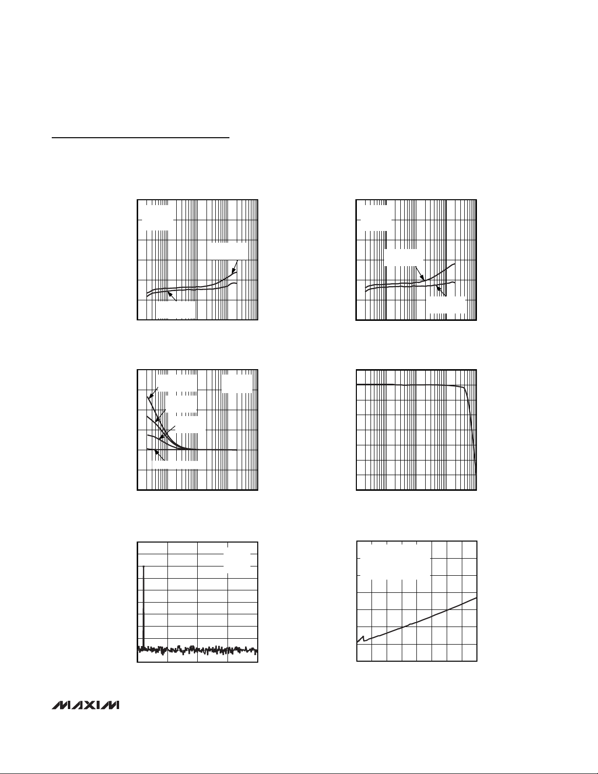
MAX9723
Stereo DirectDrive Headphone Amplifier
with BassMax, Volume Control, and I2C
_______________________________________________________________________________________ 7
CROSSTALK
vs. FREQUENCY
-100
-80
-60
-40
-20
0
-120
MAX9723 toc16
FREQUENCY (Hz)
CROSSTALK (dB)
10k1k10010 100k
VIN = 1V
P-P
RL = 32
Ω
A = 0dB
LEFT TO RIGHT
A = 0dB
RIGHT TO LEFT
A = 0dB
CROSSTALK
vs. FREQUENCY
-100
-80
-60
-40
-20
0
-120
MAX9723 toc17
FREQUENCY (Hz)
CROSSTALK (dB)
10k1k10010 100k
VIN = 1V
P-P
RL = 32
Ω
A = -10dB
LEFT TO RIGHT
A = -10dB
RIGHT TO LEFT
A = -10dB
BASS BOOST FREQUENCY
RESPONSE
-5
0
5
10
15
20
-10
MAX9723 toc18
FREQUENCY (Hz)
AMPLITUDE (dB)
10k1k10010 100k
NO LOAD
R1 = 47k
Ω
BassMax DISABLED
R2 = 36k
Ω
C3 = 0.068μF
R2 = 22k
Ω
C3 = 0.1μF
R2 = 10k
Ω
C3 = 0.22μF
GAIN FLATNESS
vs. FREQUENCY
-6
-5
-4
-3
-2
-1
0
1
-7
MAX9723 toc19
FREQUENCY (Hz)
AMPLITUDE (dB)
10k1k10010 100k
OUTPUT SPECTRUM
vs. FREQUENCY
MAX9723 toc20
FREQUENCY (kHz)
AMPLITUDE (dBV)
15105
-130
-120
-110
-100
-90
-80
-70
-60
-50
-40
-140
020
RL = 32
Ω
V
DD
= 3V
f
IN
= 1kHz
CHARGE-PUMP OUTPUT VOLTAGE
vs. OUTPUT CURRENT
MAX9723 toc21
OUTPUT CURRENT (mA)
OUTPUT VOLTAGE (V)
175150125100755025
-3.0
-2.5
-2.0
-1.5
-1.0
-0.5
0
-3.5
0200
NO HEADPHONE LOAD
CHARGE-PUMP LOAD
CONNECTED
BETWEEN PV
SS
AND PGND
Typical Operating Characteristics (continued)
(VDD= SHDN = 3V, PGND = SGND = 0V, C1 = C2 = 1µF, BB_ = 0V, gain = 0dB, maximum volume, BassMax disabled. Load connected between OUT_ and SGND where specified. Outputs in phase, both channels loaded. T
A
= +25°C, unless otherwise noted.)
(See Functional Diagram/Typical Operating Circuit)
Page 8
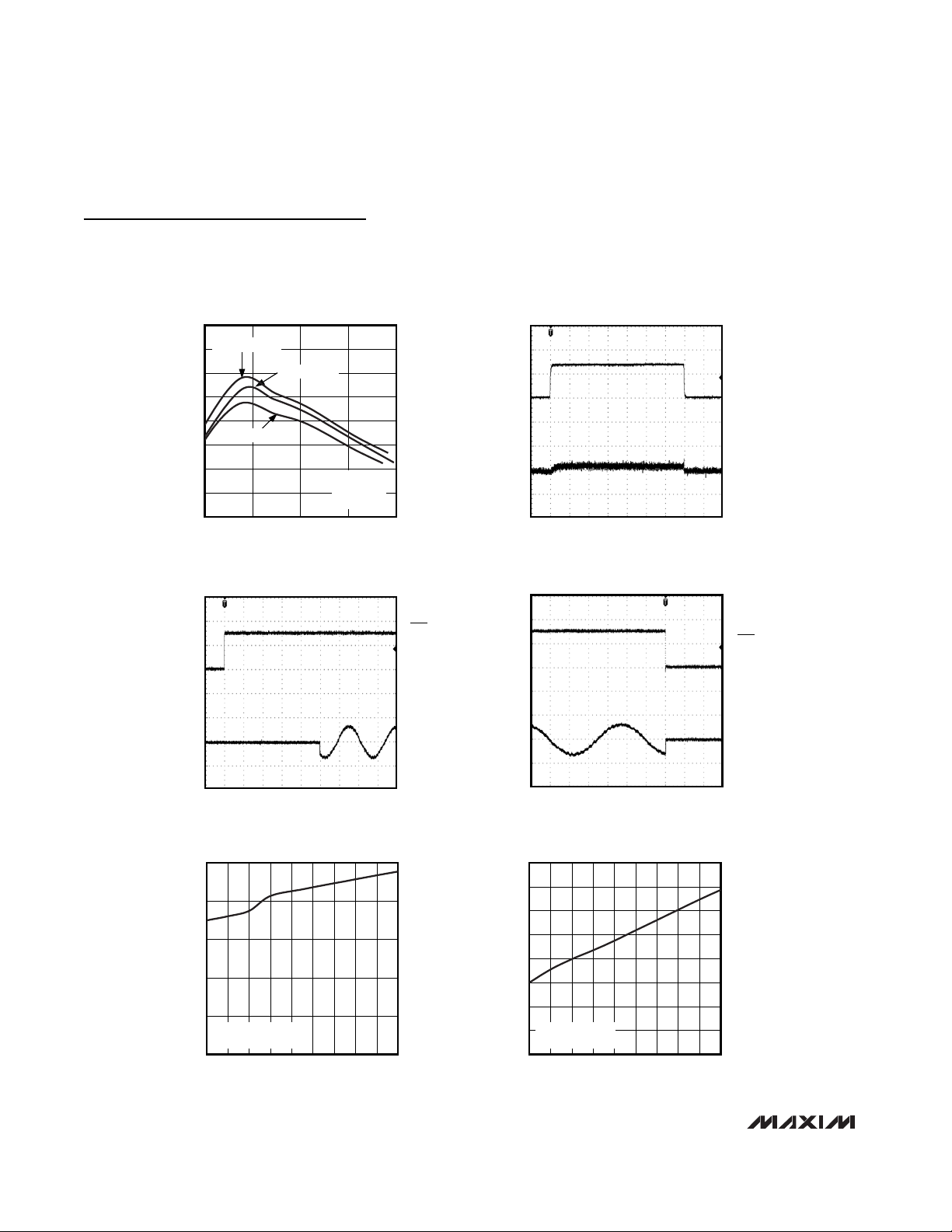
MAX9723
Stereo DirectDrive Headphone Amplifier
with BassMax, Volume Control, and I2C
8 _______________________________________________________________________________________
Typical Operating Characteristics (continued)
(VDD= SHDN = 3V, PGND = SGND = 0V, C1 = C2 = 1µF, BB_ = 0V, gain = 0dB, maximum volume, BassMax disabled. Load connected between OUT_ and SGND where specified. Outputs in phase, both channels loaded. T
A
= +25°C, unless otherwise noted.)
(See Functional Diagram/Typical Operating Circuit)
OUTPUT POWER vs. CHARGE-PUMP
CAPACITANCE AND LOAD RESISTANCE
MAX9723 toc22
LOAD RESISTANCE (Ω)
OUTPUT POWER (mW)
403020
40
45
50
55
60
65
70
75
35
10 50
C1 = C2 = 2.2μF
C1 = C2 = 0.68μF
C1 = C2 = 1μF
VDD = 3V
f
IN
= 1kHz
THD+N = 1%
POWER-UP/POWER-DOWN
WAVEFORM
MAX9723 toc23
20ms/div
V
DD
2V/div
V
OUT
10mV/div
EXITING SHUTDOWN
MAX9723 toc24
40μs/div
V
OUT_
200mV/div
V
SHDN
2V/div
ENTERING SHUTDOWN
MAX9723 toc25
20μs/div
V
OUT_
200mV/div
V
SHDN
2V/div
SUPPLY CURRENT
vs. SUPPLY VOLTAGE
MAX9723 toc26
SUPPLY VOLTAGE (V)
SUPPLY CURRENT (mA)
3.43.23.02.82.62.42.22.0
2.5
3.0
3.5
4.0
4.5
2.0
1.8 3.6
NO LOAD
INPUTS GROUNDED
SHUTDOWN CURRENT
vs. SUPPLY VOLTAGE
SHUTDOWN CURRENT (μA)
1
2
3
4
5
6
7
8
0
MAX9723 toc27
SUPPLY VOLTAGE (V)
3.43.23.02.82.62.42.22.01.8 3.6
NO LOAD
INPUTS GROUNDED
Page 9

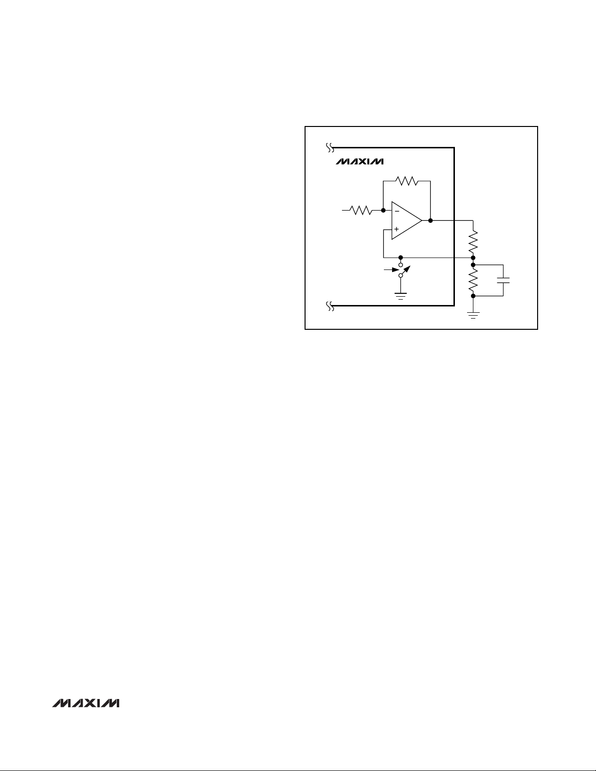
Detailed Description
The MAX9723 stereo headphone amplifier features
Maxim’s patented DirectDrive architecture, eliminating
the large output-coupling capacitors required by conventional single-supply headphone amplifiers. The
MAX9723 consists of two 62mW Class AB headphone
amplifiers, hardware/software shutdown control, inverting
charge pump, integrated 32-level volume control,
BassMax circuitry, comprehensive click-and-pop suppression circuitry, and an I2C-compatible interface (see
the Functional Diagram/Typical Operating Circuit). A
negative power supply (PVSS) is created internally by
inverting the positive supply (VDD). Powering the amplifiers from VDDand PVSSincreases the dynamic range of
the amplifiers to almost twice that of other single-supply
amplifiers, increasing the total available output power.
The MAX9723 DirectDrive outputs are biased at SGND
(see Figure 1). The benefit of this 0V bias is that the
amplifier outputs do not have a DC component, eliminating the need for large DC-blocking capacitors.
Eliminating the DC-blocking capacitors on the output
saves board space, system cost, and improves low-frequency response.
An I
2
C-compatible interface allows serial communication between the MAX9723 and a microcontroller. The
MAX9723 is available with two different I2C addresses
allowing two MAX9723 ICs to share the same bus (see
Table 1). The internal command register controls the
shutdown status of the MAX9723, enables the BassMax
circuitry, sets the maximum gain of the amplifier, and
sets the volume level (see Table 2). The MAX9723’s
BassMax circuitry improves audio reproduction by
boosting the bass response of the amplifier, compensating for any low-frequency attenuation introduced by
MAX9723
Stereo DirectDrive Headphone Amplifier
with BassMax, Volume Control, and I2C
_______________________________________________________________________________________ 9
Pin Description
PIN BUMP
THIN QFN
UCSP
NAME FUNCTION
1D1VDDPower-Supply Input. Bypass VDD to PGND with a 1µF capacitor.
2 C1 C1P Charge-Pump Flying Capacitor Positive Terminal
3 B1 PGND Power Ground. Connect to SGND.
4 A1 C1N Charge-Pump Flying Capacitor Negative Terminal
5 B2 SCL Serial Clock Input. Connect a 10kΩ pullup resistor from SCL to VDD.
6A2PV
SS
Charge-Pump Output. Connect to SVSS. Bypass PVSS with a 1µF capacitor
to PGND.
7 A3 SDA Serial-Data Input. Connect a 10kΩ pullup resistor from SDA to VDD.
8B3SHDN
Shutdown. Drive SHDN low to disable the MAX9723. Connect SHDN to V
DD
while bit 7
is high for normal operation (see the Command Register section).
9 A4 SGND Signal Ground. Connect to PGND.
10 B4 INL Left-Channel Input
11 C4 INR Right-Channel Input
12 D4 SV
SS
Headphone Amplifier Negative Power-Supply Input. Connect to PVSS.
13 C3 BBR
Right BassMax Input. Connect an external lowpass filter between OUTR and BBR to
apply bass boost to the right-channel output. Connect BBR to SGND if BassMax is not
used (see the BassMax (Bass Boost) section).
14 D3 OUTR Right Headphone Output
15 D2 OUTL Left Headphone Output
16 C2 BBL
Left BassMax Input. Connect an external lowpass filter between OUTL and BBL to
apply bass boost to the left-channel output. Connect BBL to SGND if BassMax is not
used (see the BassMax (Bass Boost) section).
EP — EP Exposed Paddle. Connect EP to SVSS or leave unconnected.
Page 10

MAX9723
the headphone. The MAX9723A and MAX9723B have a
maximum amplifier gain of 0dB while the MAX9723C
and MAX9723D have a maximum gain of +6dB.
Amplifier volume is digitally programmable to any one
of 32 levels.
DirectDrive
Traditional single-supply headphone amplifiers have
their outputs biased at a nominal DC voltage, typically
half the supply, for maximum dynamic range. Large coupling capacitors are needed to block this DC bias from
the headphone. Without these capacitors, a significant
amount of DC current flows to the headphone, resulting
in unnecessary power dissipation and possible damage
to both headphone and headphone amplifier.
Maxim’s patented DirectDrive architecture uses a charge
pump to create an internal negative supply voltage. This
allows the MAX9723 headphone amplifier outputs to be
biased at 0V, almost doubling the dynamic range while
operating from a single supply. With no DC component,
there is no need for the large DC-blocking capacitors.
Instead of two large (typically 220µF) tantalum capacitors, the MAX9723 charge pump requires only two small
1µF ceramic capacitors, thereby conserving board
space, reducing cost, and improving the low-frequency
response of the headphone amplifier. See the Output
Power vs. Charge-Pump Capacitance and Load
Resistance graph in the Typical Operating Characteris-
tics for details of the possible capacitor sizes.
In addition to the cost and size disadvantages, the DCblocking capacitors required by conventional headphone amplifiers limit low-frequency response and can
distort the audio signal.
Previous attempts at eliminating the output-coupling
capacitors involved biasing the headphone return
(sleeve) to the DC bias voltage of the headphone
amplifiers. This method raises some issues:
1) The sleeve is typically grounded to the chassis.
Using the midrail biasing approach, the sleeve must
be isolated from system ground, complicating product design. The DirectDrive output biasing scheme
allows the sleeve to be grounded.
2) During an ESD strike, the amplifier’s ESD structure is
the only path to system ground. The amplifier must
be able to withstand the full ESD strike. The
MAX9723 headphone outputs can withstand an
±8kV ESD strike (HBM).
3) When using the headphone jack as a line out to
other equipment, the bias voltage on the sleeve may
conflict with the ground potential from other equipment, resulting in possible damage to the amplifiers.
The DirectDrive outputs of the MAX9723 can be
directly coupled to other ground-biased equipment.
Charge Pump
The MAX9723 features a low-noise charge pump. The
600kHz switching frequency is well beyond the audio
range, and does not interfere with the audio signals.
This enables the MAX9723 to achieve a 99dB SNR. The
switch drivers feature a controlled switching speed that
minimizes noise generated by turn-on and turn-off transients. Limiting the switching speed of the charge
pump minimizes di/dt noise caused by the parasitic
bond wire and trace inductance. Although not typically
required, additional high-frequency noise attenuation
can be achieved by increasing the size of C2 (see the
Functional Diagram/Typical Operating Circuit).
Shutdown
The MAX9723 features a 5µA, low-power shutdown
mode that reduces quiescent current consumption and
extends battery life. Shutdown is controlled by a hardware or software interface. Driving SHDN low disables
the drive amplifiers, bias circuitry, charge pump, and
sets the headphone amplifier output impedance to
20kΩ. Similarly, the MAX9723 enters shutdown when bit
seven (B7) in the control register is reset. SHDN and B7
must be high to enable the MAX9723. The I
2
C interface
is active and the contents of the command register are
not affected when in shutdown. This allows the master
to write to the MAX9723 while in shutdown.
Stereo DirectDrive Headphone Amplifier
with BassMax, Volume Control, and I2C
10 ______________________________________________________________________________________
V
DD
+V
DD
-V
DD
VDD/2
GND
SGND
CONVENTIONAL AMPLIFIER BIASING SCHEME
DirectDrive BIASING SCHEME
Figure 1. Traditional Amplifier Output vs. MAX9723 DirectDrive
Output
Page 11
Click-and-Pop Suppression
The output-coupling capacitor is a major contributor of
audible clicks and pops in conventional single-supply
headphone amplifiers. The amplifier charges the coupling capacitor to its output bias voltage at startup.
During shutdown the capacitor is discharged. This
charging and discharging results in a DC shift across
the capacitor, which appears as an audible transient at
the speaker. Since the MAX9723 headphone amplifier
does not require output-coupling capacitors, no audible transients occur.
Additionally, the MAX9723 features extensive click-andpop suppression that eliminates any audible transient
sources internal to the device. The Power-Up/PowerDown Waveform in the Typical Operating Characteristics
shows that there are minimal transients at the output upon
startup or shutdown.
In most applications, the preamplifier driving the
MAX9723 has a DC bias of typically half the supply.
The input-coupling capacitor is charged to the preamplifier’s bias voltage through the MAX9723’s input
impedance (RIN) during startup. The resulting voltage
shift across the capacitor creates an audible click/pop.
To avoid clicks/pops caused by the input filter, delay
the rise of SHDN by at least 4 time constants, 4 x RINx
CIN, relative to the start of the preamplifier.
BassMax (Bass Boost)
Typical headphones do not have a flat-frequency
response. The small physical size of the diaphragm
does not allow the headphone speaker to efficiently
reproduce low frequencies. This physical limitation
results in attenuated bass response. The MAX9723
includes a bass boost feature that compensates for the
headphone’s poor bass response by increasing the
amplifier gain at low frequencies.
The DirectDrive output of the MAX9723 has more headroom than typical single-supply headphone amplifiers.
This additional headroom allows boosting the bass frequencies without the output-signal clipping.
Program the BassMax gain and cutoff frequency with
external components connected between OUT_ and
BB_ (see the Functional Diagram/Typical Operating
Circuit). Use the I2C-compatible interface to program the
command register to enable/disable the BassMax circuit.
BB_ is connected to the noninverting input of the output
amplifier when BassMax is enabled. BB_ is pulled to
SGND when BassMax is disabled. The typical application
of the BassMax circuit involves feeding a lowpass version
of the output signal back to the amplifier. This is realized
using positive feedback from OUT_ to BB_. Figure 2
shows the connections needed to implement BassMax.
Maximum Gain Control
The MAX9723A and MAX9723B have selectable
maximum gains of -5dB or 0dB (see Table 5) while
the MAX9723C and MAX9723D have selectable maximum gains of +1dB or +6dB (see Table 6). Bit 5 in the
command register selects between the two maximum
gain settings.
Volume Control
The MAX9723 includes a 32-level volume control that
adjusts the gain of the output amplifiers according to
the code contained in the command register. Volume is
programmed through the command register bits [4:0].
Tables 7–10 show all of the available gain settings for
the MAX9723A–MAX9723D. The mute attenuation is
typically better than 100dB when driving a 32Ω load.
Serial Interface
The MAX9723 features an I2C/SMBus-compatible,
2-wire serial interface consisting of a serial data line
(SDA) and a serial clock line (SCL). SDA and SCL facilitate communication between the MAX9723 and the
master at clock rates up to 400kHz. Figure 3 shows the
2-wire interface timing diagram. The MAX9723 is a
receive-only slave device relying on the master to generate the SCL signal. The MAX9723 cannot write to the
SDA bus except to acknowledge the receipt of data
MAX9723
Stereo DirectDrive Headphone Amplifier
with BassMax, Volume Control, and I2C
______________________________________________________________________________________ 11
C3
R2
R1
R
R
OUT_
BB_
AUDIO
INPUT
MAX9723
BassMax
ENABLE
Figure 2. BassMax External Connections
Page 12

MAX9723
from the master. The master, typically a microcontroller,
generates SCL and initiates data transfer on the bus.
A master device communicates to the MAX9723 by
transmitting the proper address followed by the data
word. Each transmit sequence is framed by a START (S)
or REPEATED START (Sr) condition and a STOP (P) condition. Each word transmitted over the bus is 8 bits long
and is always followed by an acknowledge clock pulse.
The MAX9723 SDA line operates as both an input and
an open-drain output. A pullup resistor, greater than
500Ω, is required on the SDA bus. The MAX9723 SCL
line operates as an input only. A pullup resistor, greater
than 500Ω, is required on SCL if there are multiple masters on the bus, or if the master in a single-master system has an open-drain SCL output. Series resistors in
line with SDA and SCL are optional. Series resistors
protect the digital inputs of the MAX9723 from highvoltage spikes on the bus lines, and minimize crosstalk
and undershoot of the bus signals.
Bit Transfer
One data bit is transferred during each SCL cycle. The
data on SDA must remain stable during the high period
of the SCL pulse. Changes in SDA while SCL is high
are control signals (see the START and STOP
Conditions section). SDA and SCL idle high when the
I2C bus is not busy.
Start and Stop Conditions
SDA and SCL idle high when the bus is not in use. A
master device initiates communication by issuing a
START condition. A START condition is a high-to-low
transition on SDA with SCL high. A STOP condition is a
low-to-high transition on SDA while SCL is high (Figure
4). A START condition from the master signals the beginning of transmission to the MAX9723. The master terminates transmission and frees the bus by issuing a STOP
condition. The bus remains active if a REPEATED START
condition is generated instead of a STOP condition.
Early STOP Conditions
The MAX9723 recognizes a STOP condition at any point
during data transmission except if the STOP condition
occurs in the same high pulse as a START condition.
Slave Address
The MAX9723 is available with one of two preset slave
addresses (see Table 1). The address is defined as the
seven most significant bits (MSBs) followed by the
Read/Write (R/W) bit. The address is the first byte of
information sent to the MAX9723 after the START condition. The MAX9723 is a slave device only capable of
being written to. The sent R/W bit must always be a
zero when configuring the MAX9723.
The MAX9723 acknowledges the receipt of its address
even if R/W is set to 1. However, the MAX9723 will not
drive SDA. Addressing the MAX9723 with R/W set to 1
causes the master to receive all 1’s regardless of the
contents of the command register.
Acknowledge
The acknowledge bit (ACK) is a clocked 9th bit that the
MAX9723 uses to handshake receipt of each byte of
Stereo DirectDrive Headphone Amplifier
with BassMax, Volume Control, and I2C
12 ______________________________________________________________________________________
SCL
SDA
START
CONDITION
STOP
CONDITION
REPEATED
START
CONDITION
START
CONDITION
t
HD, STA
t
SU, STA
t
HD, STA
t
SP
t
BUF
t
SU, STO
t
LOW
t
SU, DAT
t
HD, DAT
t
HIGH
t
R
t
F
Figure 3. 2-Wire Serial-Interface Timing Diagram
Page 13

data (see Figure 5). The MAX9723 pulls down SDA during the master-generated 9th clock pulse. The SDA line
must remain stable and low during the high period of
the acknowledge clock pulse. Monitoring ACK allows
for detection of unsuccessful data transfers. An unsuccessful data transfer occurs if a receiving device is
busy or if a system fault has occurred. In the event of
an unsuccessful data transfer, the bus master may
reattempt communication.
Write Data Format
A write to the MAX9723 includes transmission of a
START condition, the slave address with the R/W bit
reset to 0 (see Table 1), one byte of data to configure
the command register, and a STOP condition. Figure 6
illustrates the proper format for one frame.
The MAX9723 only accepts write data, but it acknowledges the receipt of its address byte with the R/W bit
set high. The MAX9723 does not write to the SDA bus
in the event that the R/W bit is set high. Subsequently,
the master reads all 1’s from the MAX9723. Always
reset the R/W bit to 0 to avoid this situation.
Command Register
The MAX9723 has one command register that is used
to enable/disable shutdown, enable/disable BassMax,
and set the maximum gain and volume. Table 2
describes the function of the bits contained in the command register.
Reset B7 to 0 to shut down the MAX9723. The MAX9723
wakes up from shutdown when B7 is set to 1 provided
SHDN is high. SHDN must be high and B7 must be set to
1 for the MAX9723 to operate normally (see Table 3).
Set B6 to 1 to enable BassMax (see Table 4). The output
signal’s low-frequency response will be boosted according to the external components connected between
OUT_ and BB_. See the BassMax Gain-Setting
Components section in the Applications Information sec-
tion for details on choosing the external components.
MAX9723
Stereo DirectDrive Headphone Amplifier
with BassMax, Volume Control, and I2C
______________________________________________________________________________________ 13
SCL
SDA
SSrP
Figure 4. START, STOP, and REPEATED START Conditions
1
SCL
START
CONDITION
SDA
289
CLOCK PULSE FOR
ACKNOWLEDGMENT
ACKNOWLEDGE
NOT ACKNOWLEDGE
Figure 5. Acknowledge
MAX9723 SLAVE ADDRESS
PART
R/W
MAX9723A
0
MAX9723B
0
MAX9723C
0
MAX9723D
0
Table 1. MAX9723 Address Map
B7 B6 B5
B0
SHUTDOWN
BassMax
MAXIMUM
GAIN
VOLUME
Table 2. MAX9723 Command Register
MODE B7
MAX9723 Disabled 0
MAX9723 Enabled 1
Table 3. Shutdown Control, SHDN = 1
MODE B6
BassMax Disabled 0
BassMax Enabled 1
Table 4. BassMax Control
A6 A5 A4 A3 A2 A1 A0
1001100
1001101
1001100
1001101
ENABLE
B4 B3 B2 B1
Page 14

MAX9723
The MAX9723A and MAX9723B have a maximum gain
setting of -5dB or 0dB, while the MAX9723C and
MAX9723D have a maximum gain setting of +1dB or
+6dB. B5 in the command register programs the maximum gain (see Tables 5 and 6).
Adjust the MAX9723’s amplifier gain with the volume
control bits [4:0]. The gain is adjustable to one of 32
steps ranging from full mute to the maximum gain programmed by B5. Tables 7–10 list all the possible gain
settings for the MAX9723. Figures 7–10 show the volume control transfer functions for the MAX9723.
Power-On Reset
The contents of the MAX9723’s command register at
power-on are shown in Table 11.
Applications Information
Power Dissipation and Heat Sinking
Linear power amplifiers can dissipate a significant
amount of power under normal operating conditions.
The maximum power dissipation for each package is
given in the Absolute Maximum Ratings section under
Continuous Power Dissipation or can be calculated by
the following equation:
where T
J(MAX)
is +150°C, TAis the ambient tempera-
ture, and θJAis the reciprocal of the derating factor in
°C/W as specified in the Absolute Maximum Ratings
section. For example, θJAfor the thin QFN package is
+59°C/W.
The MAX9723 has two power dissipation sources, the
charge pump and the two output amplifiers. If the
power dissipation exceeds the rated package dissipa-
tion, reduce V
DD
, increase load impedance, decrease
the ambient temperature, or add heatsinking. Large
output, supply, and ground traces decrease θ
JA
, allowing more heat to be transferred from the package to
surrounding air.
Output Dynamic Range
Dynamic range is the difference between the noise
floor of the system and the output level at 1% THD+N. It
is essential that a system’s dynamic range be known
before setting the maximum output gain. Output clipping will occur if the output signal is greater than the
dynamic range of the system. The DirectDrive architecture of the MAX9723 has increased dynamic range
compared to other single-supply amplifiers.
Use the THD+N vs. Output Power in the Typical
Operating Characteristics to identify the system’s
dynamic range. Find the output power that causes 1%
THD+N for a given load. This point will indicate what
output power causes the output to begin to clip. Use
the following equation to determine the peak output
voltage that causes 1% THD+N for a given load.
where P
OUT_1%
is the output power that causes 1%
THD+N, RLis the load resistance, and V
OUT_(P-P)
is the
peak output voltage. After V
OUT_(P-P)
is identified,
determine the peak input voltage that can be amplified
without clipping:
where V
IN_(P-P)
is the largest peak voltage that can be
amplified without clipping, and AVis the voltage gain of
V
V
IN P P
OUT P P
A
V
_( )
_( )−−
⎛
⎝
⎜
⎞
⎠
⎟
=
10
20
VPR
OUT P P OUT L_( ) _ %
()
−
=×22
1
P
TT
D MAX
J MAX A
JA
()
()
=
−
θ
Stereo DirectDrive Headphone Amplifier
with BassMax, Volume Control, and I2C
14 ______________________________________________________________________________________
S
ACK
0
ACKNOWLEDGE FROM MAX9723
R/W
ACKNOWLEDGE
FROM MAX9723
B7 B6
B5
B4
B3 B2
COMMAND BYTE IS STORED ON
RECEIPT OF STOP CONDITION
ACK
P
B1 B0
SLAVE ADDRESS COMMAND BYTE
Figure 6. Write Data Format Example
MAXIMUM GAIN (dB) B5
-5 0
01
Table 5. MAX9723A and MAX9723B
Maximum Gain Control
MAXIMUM GAIN (dB) B5
+1 0
+6 1
Table 6. MAX9723C and MAX9723D
Maximum Gain Control
Page 15
the amplifier in dB determined by the maximum gain setting (Bit 5) or the combination of the maximum gain setting plus bass boost (see the BassMax Gain-Setting
Components section).
Component Selection
Input-Coupling Capacitor
The AC-coupling capacitor (CIN) and internal gain-setting resistor form a highpass filter that removes any DC
bias from an input signal (see the Functional Diagram/
Typical Operating Circuit). CINallows the MAX9723 to
bias the signal to an optimum DC level. The -3dB point
MAX9723
Stereo DirectDrive Headphone Amplifier
with BassMax, Volume Control, and I2C
______________________________________________________________________________________ 15
B4 B3
B2
B1
B0
GAIN
(dB)
11111 0
11110 -0.5
11101 -1
11100 -1.5
11011 -2
11010 -2.5
11001 -3
11000 -4
10111 -5
10110 -6
10101 -7
10100 -9
1 0 0 1 1 -11
1 0 0 1 0 -13
1 0 0 0 1 -15
1 0 0 0 0 -17
0 1 1 1 1 -19
0 1 1 1 0 -21
0 1 1 0 1 -23
0 1 1 0 0 -25
0 1 0 1 1 -27
0 1 0 1 0 -29
0 1 0 0 1 -31
0 1 0 0 0 -33
0 0 1 1 1 -35
0 0 1 1 0 -37
0 0 1 0 1 -39
0 0 1 0 0 -41
0 0 0 1 1 -43
0 0 0 1 0 -45
0 0 0 0 1 -47
0 0 0 0 0 MUTE
Table 7. MAX9723A and MAX9723B Gain
Settings (B5 = 1, Max Gain = 0dB)
B4 B3 B2 B1
B0
GAIN
(dB)
1
-5
1
-6
1
-7
1
-9
1
-11
11010-13
1
-15
11000-17
1
-19
1
-21
1
-23
1
-25
1
-27
1
-29
1
-31
1
-33
0
-35
0
-37
01101-39
0
-41
01011-43
0
-45
0
-47
0
-51
0
-55
0
-59
0
-63
0
-67
0
-71
00010-75
0
-79
00000
MUTE
Table 8. MAX9723A and MAX9723B Gain
Settings (B5 = 0, Max Gain = -5dB)
(LSB)
(LSB)
1111
1110
1101
1100
1011
1001
0111
0110
0101
0100
0011
0010
0001
0000
1111
1110
1100
1010
1001
1000
0111
0110
0101
0100
0011
0001
Page 16
MAX9723
of the highpass filter, assuming zero-source impedance, is given by:
f
RC
dB
IN IN
−
=
××
3
1
2π
Stereo DirectDrive Headphone Amplifier
with BassMax, Volume Control, and I2C
16 ______________________________________________________________________________________
B4 B3 B2 B1
B0
GAIN
(dB)
111111
111100
11101-1
11100-3
11011-5
11010-7
11001-9
11000-11
10111-13
10110-15
10101-17
10100-19
10011-21
10010-23
10001-25
10000-27
01111-29
01110-31
01101-33
01100-35
01011-37
01010-39
01001-41
01000-45
00111-49
00110-53
00101-57
00100-61
00011-65
00010-69
00001-73
00000
MUTE
Table 10. MAX9723C and MAX9723D Gain
Settings (B5 = 0, Max Gain = +1dB)
MODE
B0
Power-On
Reset
1
Table 11. Initial Power-Up Command
Register Status
B4 B3 B2 B1
B0
GAIN
(dB)
111116
111105.5
111015
111004.5
110114
110103.5
110013
110002
101111
101100
10101-1
10100-3
10011-5
10010-7
10001-9
10000-11
01111-13
01110-15
01101-17
01100-19
01011-21
01010-23
01001-25
01000-27
00111-29
00110-31
00101-33
00100-35
00011-37
00010-39
00001-41
00000
MUTE
Table 9. MAX9723C and MAX9723D Gain
Settings (B5 = 1, Max Gain = +6dB)
(LSB)
(LSB)
B7 B6 B5 B4 B3 B2 B1
1111111
Page 17
where RINis a minimum of 10kΩ. Choose CINsuch that
f
-3dB
is well below the lowest frequency of interest.
Setting f
-3dB
too high affects the amplifier’s low-frequency response. Use capacitors with low-voltage coefficient
dielectrics. Film or C0G dielectric capacitors are good
choices for AC-coupling capacitors. Capacitors with
high-voltage coefficients, such as ceramics, can result in
increased distortion at low frequencies.
Charge-Pump Flying Capacitor
The charge-pump flying capacitor connected between
C1N and C1P affects the charge pump’s load regulation and output impedance. Choosing a flying capacitor
that is too small degrades the MAX9723’s ability to provide sufficient current drive and leads to a loss of output voltage. Increasing the value of the flying capacitor
improves load regulation and reduces the chargepump output impedance. See the Output Power vs.
MAX9723
Stereo DirectDrive Headphone Amplifier
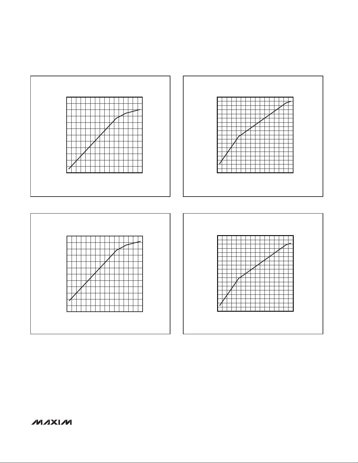
with BassMax, Volume Control, and I2C
______________________________________________________________________________________ 17
MAX9723A AND MAX9723B
TRANSFER FUNCTION (B5 = 1)
CODE
GAIN (dB)
-20
-30
-40
10
0
-10
-50
0 6 12 18 24 30
Figure 7. MAX9723A/MAX9723B Transfer Function with B5 = 1
MAX9723A AND MAX9723B
TRANSFER FUNCTION (B5 = 0)
CODE
GAIN (dB)
-40
-50
-60
-70
-80
0
-10
-30
-20
-90
0 6 12 18 24 30
Figure 8. MAX9723A/MAX9723B Transfer Function with B5 = 0
MAX9723C AND MAX9723D
TRANSFER FUNCTION (B5 = 0)
CODE
0 6 12 18 24 30
GAIN (dB)
-30
-40
-50
-60
-70
10
0
-20
-10
-80
Figure 10. MAX9723C/MAX9723D Transfer Function with B5 = 0
MAX9723C AND MAX9723D
TRANSFER FUNCTION (B5 = 1)
CODE
GAIN (dB)
-30
-40
10
0
-20
-10
-50
0 6 12 18 24 30
Figure 9. MAX9723C/MAX9723D Transfer Function with B5 = 1
Page 18

MAX9723
Charge-Pump Capacitance and Load Resistance
graph in the Typical Operating Characteristics.
Charge-Pump Hold Capacitor
The hold capacitor’s value and ESR directly affect the
ripple at PVSS. Ripple is reduced by increasing the value
of the hold capacitor. Choosing a capacitor with lower
ESR reduces ripple and output impedance. Lower
capacitance values can be used in systems with low
maximum output power levels. See the Output Power vs.
Charge-Pump Capacitance and Load Resistance graph
in the Typical Operating Characteristics.
BassMax Gain-Setting Components
The bass-boost low-frequency response, when
BassMax is enabled, is set by the ratio of R1 to R2 by
the following equation (see Figure 2):
where A
V_BOOST
is the voltage gain boost in dB at low
frequencies. A
V_BOOST
is added to the gain realized by
the volume setting. The absolute gain at low frequencies is equal to:
where A
V_VOL
is the gain due to the volume setting,
and A
V_TOTAL
is the absolute gain at low frequencies.
To maintain circuit stability, the ratio:
R2/(R1 + R2)
must not exceed 1/2. A ratio equaling 1/3 is recommended. The switch that shorts BB_ to SGND, when
BassMax is disabled, can have an on-resistance as
high as 300Ω. Choose a value for R1 that is greater
than 40kΩ to ensure that positive feedback is negligible
when BassMax is disabled. Table 12 contains a list of
R2 values, with R1 = 47kΩ, and the corresponding lowfrequency gain.
The low-frequency boost attained by the BassMax circuit is added to the gain realized by the volume setting.
Select the BassMax gain so that the output signal will
remain within the dynamic range of the MAX9723.
Output signal clipping will occur at low frequencies if
the BassMax gain boost is excessively large (see the
Output Dynamic Range section).
Capacitor C3 forms a pole and a zero according to the
following equations:
f
POLE
is the frequency at which the gain boost begins
to roll off. f
ZERO
is the frequency at which the bassboost gain no longer affects the transfer function and
the volume-control gain dominates. Table 13 contains a
list of capacitor values and the corresponding poles
and zeros for a given DC gain. See Figure 11 for an
example of a gain profile using BassMax.
Custom Maximum Gain Setting Using
BassMax
The circuit in Figure 12 uses the BassMax function to
increase the maximum gain of the MAX9723. The gain
boost created with the circuit in Figure 12 is added to
the maximum gain selected by Bit 5 in the command
register. Set the maximum gain with RA and RB using
the following equation:
where A
V_VOL
is the gain due to the volume setting,
and A
V_TOTAL
is the absolute passband gain in dB.
Capacitor CA blocks any DC offset from being gained,
but allows higher frequencies to pass. CA creates a
pole that indicates the low-frequency point of the pass
band. Choose CA so that the lowest frequencies of
AA
RA RB
RA RB
V TOTAL V VOL__
log=+×
+
−
⎛
⎝
⎜
⎞
⎠
⎟
20
f
RR
CRR
f
RR
CRR
POLE
ZERO
=
−
×××
=
+
×××
12
2312
12
2312
π
π
AAA
V TOTAL V VOL V BOOST___
=+
A
RR
RR
V BOOST_
log=×
+
−
20
12
12
Stereo DirectDrive Headphone Amplifier
with BassMax, Volume Control, and I2C
18 ______________________________________________________________________________________
GAIN PROFILE WITH AND
WITHOUT BassMax
FREQUENCY (Hz)
A
V
(dB)
1k10010
-8
-6
-4
-2
0
2
4
6
8
10
-10
1 10k
MAX9723A
CMD REGISTER
CODE = 0xFF
R1 = 47kΩ
R2 = 22kΩ
C3 = 0.1μF
f
POLE
f
ZERO
WITH
BassMax
WITHOUT
BassMax
Figure 11. BassMax, Gain Profile Example
Page 19

interest are not attenuated. For a typical application, set
f
POLE
equal to or below 20Hz.
Figure 13 shows the frequency response of the circuit
in Figure 12. With RA = 47kΩ, RB = 22kΩ, and CA =
0.33µF, the passband gain is set to 8.8dB.
Layout and Grounding
Proper layout and grounding are essential for optimum
performance. Connect PGND and SGND together at a
single point on the PC board. Connect PVSSto SV
SS
and bypass with a 1µF capacitor to PGND. Bypass V
DD
to PGND with a 1µF capacitor. Place the power-supply
bypass capacitor and the charge-pump capacitors as
close to the MAX9723 as possible. Route PGND and all
traces that carry switching transients away from SGND
and the audio signal path. Route digital signal traces
away from the audio signal path. Make traces perpendicular to each other when routing digital signals over
or under audio signals.
The thin QFN package features an exposed paddle
that improves thermal efficiency. Ensure that the
exposed paddle is electrically isolated from PGND,
SGND, and VDD. Connect the exposed paddle to
SV
SS
when the board layout dictates that the
exposed paddle cannot be left floating.
CA
fRARB
POLE
()
=
×−
1
2 π
MAX9723
Stereo DirectDrive Headphone Amplifier
with BassMax, Volume Control, and I2C
______________________________________________________________________________________ 19
CA
RB
RA
R
R
OUT_
BB_
AUDIO
INPUT
MAX9723
BassMax
ENABLE
Figure 12. Using BassMax to Increase MAX9723’s Maximum
Gain
R2 (kΩ)A
V
GAIN (dB)
39 20.6
33 15.1
27 11.3
22 8.8
15 5.7
10 3.7
Table 12. BassMax Gain Examples
(R1 = 47kΩ)
C3 (nF) f
POLE
(Hz) f
ZERO
(Hz)
100 38 106
82 47 130
68 56 156
56 68 190
47 81 230
22 174 490
10 384 1060
Table 13. BassMax Pole and Zero
Examples for a Gain Boost of 8.8dB
(R1 = 47kΩ, R2 = 22kΩ)
FREQUENCY RESPONSE OF FIGURE 12
FREQUENCY (Hz)
A
V
(dB)
1k100101
1
2
3
4
5
6
7
8
9
10
0
0.1 10k
MAX9723A
CMD REGISTER
CODE = 0xFF
RA = 47kΩ
RB = 22kΩ
CA = 0.33μF
Figure 13. Increasing the Maximum Gain Using BassMax
Page 20
MAX9723
UCSP Applications Information
For the latest application details on UCSP construction,
dimensions, tape carrier information, PC board techniques, bump-pad layout, and recommended reflow temperature profile, as well as the latest information on
reliability testing results, go to Maxim’s website at
www.maxim-ic.com/ucsp and look up Application Note
1891: Understanding the Basics of the Wafer-Level Chip-
Scale Package (WL-CSP).
Stereo DirectDrive Headphone Amplifier
with BassMax, Volume Control, and I2C
20 ______________________________________________________________________________________
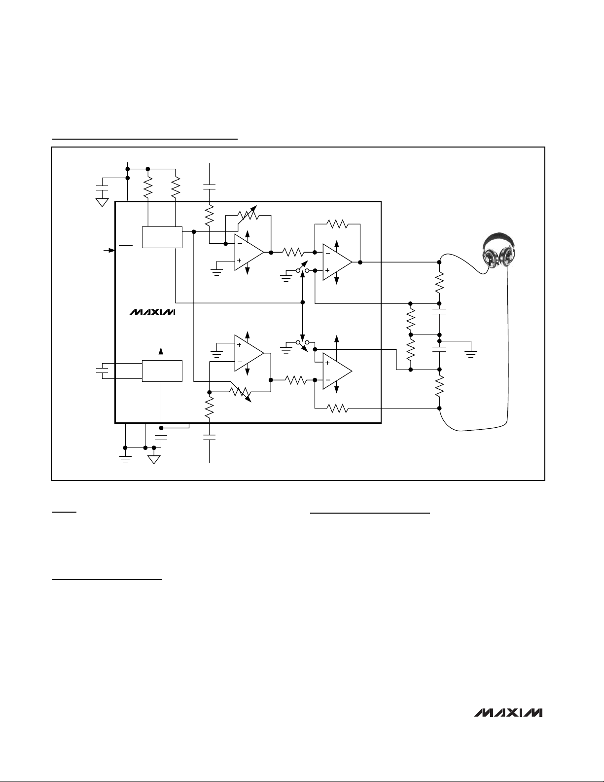
Functional Diagram/Typical Operating Circuit
R5
10k
Ω
R6
10k
Ω
C
IN
0.47μF
C4
0.1μF
R4
22k
Ω
R3
47k
Ω
R1
47k
Ω
C5
1μF
C2
1μF
C
IN
0.47μF
C1
1μF
1.8V TO 3.6V
ANALOG INPUT
I2C INTERFACE
CHARGE PUMP
V
DD
INR
SDA
SCL
V
DD
V
DD
SV
SS
V
DD
R
OUTR
BBR
BBL
OUTL
R
SV
SS
V
DD
SV
SS
V
DD
SV
SS
SHDN
C1P
C1N
SGND PGND PV
SSSVSS
C3
0.1μF
R2
22k
Ω
ANALOG INPUT
BASS BOOST CIRCUIT TUNED
FOR +8.8dB AT 106Hz.
MAX9723
R
INL
R
Chip Information
TRANSISTOR COUNT: 7165
PROCESS: BiCMOS
Page 21
MAX9723
Stereo DirectDrive Headphone Amplifier
with BassMax, Volume Control, and I2C
______________________________________________________________________________________ 21
12
11
10
9
SV
SS
INR
INL
SGND
5
678
SCL
PV
SS
SDA
SHDN
16 15 14 13
BBL
OUTL
OUTR
BBR
1
2
3
4
V
DD
C1P
PGND
C1N
MAX9723_
TOP VIEW
TOP VIEW
(BUMP SIDE DOWN)
THIN QFN
UCSP
SHDN
C1N
PV
SS
SDA SGND
INLSCLPGND
C1P
V
DD
BBL BBR
INR
OUTL OUTR
SV
SS
MAX9723_
1234
A
B
C
D
+
System Diagram
Pin Configurations
2
C
I
MASTER
R5
10k
CODEC
C
IN
0.47μF
C
IN
0.47μF
SDA
SCL
INL
INR
C1P
C1N
1.8V TO
3.6V
C2
1μF
R6
Ω
Ω
10k
C1
1μF
PV
C5
1μF
MAX9723
SS
SV
SS
V
DD
PGND SGND
OUTL
BBL
OUTR
BBR
R3
47k
R4
22k
R1
47k
R2
22k
Ω
C4
Ω
0.1μF
Ω
C3
0.1μF
Ω
Page 22

MAX9723
Stereo DirectDrive Headphone Amplifier
with BassMax, Volume Control, and I2C
22 ______________________________________________________________________________________
Package Information
(The package drawing(s) in this data sheet may not reflect the most current specifications. For the latest package outline information,
go to www.maxim-ic.com/packages
.)
24L QFN THIN.EPS
Page 23

MAX9723
Stereo DirectDrive Headphone Amplifier
with BassMax, Volume Control, and I2C
______________________________________________________________________________________ 23
Package Information (continued)
(The package drawing(s) in this data sheet may not reflect the most current specifications. For the latest package outline information,
go to www.maxim-ic.com/packages
.)
Page 24

MAX9723
Stereo DirectDrive Headphone Amplifier
with BassMax, Volume Control, and I2C
24 ______________________________________________________________________________________
Package Information (continued)
(The package drawing(s) in this data sheet may not reflect the most current specifications. For the latest package outline information,
go to www.maxim-ic.com/packages
.)
16L,UCSP.EPS
PACKAGE OUTLINE, 4x4 UCSP
21-0101
1
H
1
Page 25

MAX9723
Stereo DirectDrive Headphone Amplifier
with BassMax, Volume Control, and I2C
Maxim cannot assume responsibility for use of any circuitry other than circuitry entirely embodied in a Maxim product. No circuit patent licenses are
implied. Maxim reserves the right to change the circuitry and specifications without notice at any time.
Maxim Integrated Products, 120 San Gabriel Drive, Sunnyvale, CA 94086 408-737-7600 ____________________ 25
© 2008 Maxim Integrated Products is a registered trademark of Maxim Integrated Products, Inc.
Revision History
REVISION
NUMBER
REVISION
DATE
DESCRIPTION
PAGES
CHANGED
2 8/08
Updated TQFN pin configuration, and corrected Typical Operating Circuit and
System Diagram pin names
20, 21
 Loading...