

General Description
The MAX9718/MAX9719 differential input audio power
amplifiers are ideal for portable audio devices with
internal speakers. The differential input structure
improves noise rejection and provides common-mode
rejection. A bridge-tied load (BTL) architecture minimizes external component count, while providing highquality, power audio amplification. The MAX9718 is a
single-channel amplifier while the MAX9719 is a dualchannel amplifier for stereo systems. Both devices
deliver 1.4W continuous average power per channel to
a 4Ω load with less than 1% THD+N while operating
from a single +5V supply. The devices are available as
adjustable gain amplifiers or with internally fixed gains
of 0dB, 3dB, and 6dB to reduce component count.
A shutdown input disables the bias generator and
amplifiers and reduces quiescent current consumption
to less than 100nA. The MAX9718 shutdown input can
be set as active high or active low. These devices feature Maxim’s comprehensive click-and-pop suppression circuitry that reduces audible clicks and pops
during startup and shutdown.
The MAX9718 is pin compatible with the LM4895,
and is available in 9-bump UCSP™, 10-pin TDFN, and
10-pin µMAX
®
packages. The MAX9719 is available in
16-pin TQFN, 16-pin TSSOP, and 16-bump UCSP packages. Both devices operate over the -40°C to +85°C
extended temperature range.
Applications
Mobile Phones
PDAs
Portable Devices
Features
♦ 2.7V to 5.5V Single-Supply Operation
♦ Very High -93dB PSRR at 217Hz
♦ 1.4W into 4Ω at 1% THD+N (per Channel)
♦ Differential Input
♦ Internal Fixed Gain to Reduce Component Count
♦ Adjustable Gain Option (MAX9718A/H/MAX9719A)
♦ 100nA Low-Power Shutdown Mode
♦ No Audible Clicks or Pops at Power-Up/Down
♦ Improved Performance Pin-Compatible Upgrade
to LM4895 (MAX9718D/G)
♦ 1.8V Logic Compatible
MAX9718/MAX9719
Low-Cost, Mono/Stereo,
1.4W Differential Audio Power Amplifiers
________________________________________________________________ Maxim Integrated Products 1
Ordering Information
MAX9719
SINGLE SUPPLY
2.7V TO 5.5V
SHDN
INL+
INL-
INR+
INR-
MAX9718
SINGLE SUPPLY
2.7V TO 5.5V
SHDM
SHDN
IN+
OUT+
OUT-
OUTR-
OUTR+
OUTL-
OUTL+
IN-
Simplified Block Diagrams
19-3050; Rev 4; 9/06
For pricing, delivery, and ordering information, please contact Maxim/Dallas Direct! at
1-888-629-4642, or visit Maxim’s website at www.maxim-ic.com.
Ordering Information continued at end of data sheet.
Pin Configurations appear at end of data sheet.
EVALUATION KIT
AVAILABLE
UCSP is a trademark of Maxim Integrated Products, Inc.
µMAX is a registered trademark of Maxim Integrated Products, Inc.
+Denotes lead-free package.
*EP = Exposed paddle.
PART TEMP RANGE
MAX9718AEBL-T -40°C to +85°C 3 x 3 UCSP ADX
MAX9718AEBL+T -40°C to +85°C 3 x 3 UCSP +ADX
MAX9718AETB-T -40°C to +85°C 10 TDFN-EP* AAV
PINPACKAGE
TOP
MARK
MAX9718/MAX9719
Low-Cost, Mono/Stereo,
1.4W Differential Audio Power Amplifiers
2 _______________________________________________________________________________________
ABSOLUTE MAXIMUM RATINGS
ELECTRICAL CHARACTERISTICS—5V Supply
(VCC= 5V, GND = 0, SHDN/SHDN = VCC(MAX9718/MAX9719), SHDM = GND (MAX9718), RIN= RF= 10kΩ (MAX971_A/H),
T
A
= +25°C. C
BIAS
= 0.1µF, no load. Typical values are at TA= +25°C, unless otherwise noted.) (Note 1)
Stresses beyond those listed under “Absolute Maximum Ratings” may cause permanent damage to the device. These are stress ratings only, and functional
operation of the device at these or any other conditions beyond those indicated in the operational sections of the specifications is not implied. Exposure to
absolute maximum rating conditions for extended periods may affect device reliability.
Supply Voltage (VCCto GND) ..................................-0.3V to +6V
Any Other Pin to GND ...............................-0.3V to (V
CC
+ 0.3V)
IN_, BIAS, SHDM, SHDN, SHDN Continuous Current ........20mA
OUT_ Short-Circuit Duration to GND or V
CC
.............Continuous
Continuous Power Dissipation (T
A
= +70°C)
9-Bump UCSP (derate 5.2mW/°C above +70°C)..........412mW
10-Pin TDFN (derate 24.4mW/°C above +70°C) ........1951mW
10-Pin µMAX (derate 10.3mW/°C above +70°C) ..........825mW
16-Bump UCSP (derate 8.2mW/°C above +70°C) .......659mW
16-Pin TQFN (derate 16.9mW/°C above +70°C) ........1349mW
16-Pin TSSOP (derate 21.3mW/°C above +70°C) ......1702mW
Operating Temperature Range ...........................-40°C to +85°C
Junction Temperature .....................................................+150°C
Storage Temperature Range .............................-65°C to +150°C
Bump Temperature (soldering) Reflow............................+235°C
Lead Temperature (soldering, 10s) .................................+300°C
PARAMETER SYMBOL CONDITIONS MIN TYP MAX UNITS
Supply Voltage V
Supply Current I
Shutdown Supply Current I
SHDN, SHDN, SHDM
Threshold
SHDN, SHDN, SHDM
Threshold
Output Offset Voltage V
Common-Mode Input Voltage V
Input Impedance R
Common-Mode Rejection Ratio CMRR
Power-Supply Rejection Ratio PSRR
Output Power P
Total Harmonic Distortion Plus
Noise
CC
V
= V
= V
IN+
IN+
= V
= V
BIAS
BIAS
CC
SHDN
V
IH
V
IL
V
IH
V
IL
OS
IN-
per amplifier (Note 2)
SHDN = SHDM = SHDN = GND, per amplifier 0.1 1 µA
MAX9718A/B/C/D
MAX9718E/F/G/H
V
IN-
Inferred from
CMRR test
IC
External gain, MAX971_A/H 0.5 VCC - 1.2
MAX971_B/E, MAX971_C/F, MAX971_D/G 10 15 20 kΩ
IN
f
= 1kHz -60
N
V
= V
= V
IN+
BIAS
= 200m V
= 1µF
BIAS
= 1kHz, P
IN
= 5V, AV = 6dB (Note 5)
OUT
THD+N
IN-
V
RIPPLE
R
= 8Ω , C
L
THD+N = 1%,
= 1kHz (Note 4)
f
IN
R
= 8Ω, f
L
V
CC
2.7 5.5 V
, TA = -40°C to +85°C,
0.7 x V
5.0 7.5 mA
CC
0.3 x V
1.4
AV = 0dB, MAX971_A/H,
MAX971_B/E
±1 ±10
AV = 3dB, MAX971_C/F ±1 ±15
AV = 6dB, MAX971_D/G ±1 ±20
AV = 0dB, MAX971_B/E 0.5 V CC - 0.5
AV = 3dB, MAX971_C/F 0.5 V CC - 0.6
A
= 6dB, MAX971_D/G 0.5 V CC - 0.8
V
-50 -60
,
f = 217Hz -93
,
P-P
f = 1kHz -90
R
= 8Ω 0.8 1.1
L
R
= 4Ω 1.4
L
= 0.75W,
OUT
0.002 %
CC
0.4
V
V
mV
V
dB
dB
W
MAX9718/MAX9719
Low-Cost, Mono/Stereo,
1.4W Differential Audio Power Amplifiers
_______________________________________________________________________________________ 3
ELECTRICAL CHARACTERISTICS—5V Supply (continued)
(VCC= 5V, GND = 0, SHDN/SHDN = VCC(MAX9718/MAX9719), SHDM = GND (MAX9718), RIN= RF= 10kΩ (MAX971_A/H),
T
A
= +25°C. C
BIAS
= 0.1µF, no load. Typical values are at TA= +25°C, unless otherwise noted.) (Note 1)
ELECTRICAL CHARACTERISTICS—3V Supply
(VCC= 3V, GND = 0, SHDN/SHDN = VCC(MAX9718/MAX9719), SHDM = GND (MAX9718), RIN= RF= 10kΩ (MAX971_A/H),
T
A
= +25°C. C
BIAS
= 0.1µF, no load. Typical values are at TA= +25°C, unless otherwise noted.) (Note 1)
PARAMETER SYMBOL CONDITIONS MIN TYP MAX UNITS
Gain Accuracy MAX971_B/E, MAX971_C/F, MAX971_D/G ±1 %
Channel-to-Channel Gain
Matching
Signal-to-Noise Ratio SNR P
MAX9719B/E, MAX9719C/F, MAX9719D/G ±1 %
OUT
= 1W, R
= 8Ω -104 dB
L
Thermal-Shutdown Threshold +160 °C
Thermal-Shutdown Hysteresis 15 °C
Maximum Capacitive Drive C
Power-Up/Enable from
Shutdown Time
Shutdown Time t
Turn-Off Transient V
LOAD
t
PU
SHDN
POP
Bridge-tied capacitance 500 pF
10 ms
3.5 µs
(Note 6) 50 mV
Crosstalk MAX9719, fIN = 1kHz -85 dB
PARAMETER SYMBOL CONDITIONS MIN TYP MAX UNITS
Supply Current I
Shutdown Supply Current I
SHDN, SHDN, SHDM
Threshold
Common-Mode Bias Voltage V
Output Offset Voltage V
Common-Mode Input Voltage V
Input Impedance R
Common-Mode Rejection Ratio CMRR
Power-Supply Rejection Ratio PSRR
V
= V
CC
SHDN
V
IH
V
IL
BIAS
IN+
= V
IN-
per amplifier (Note 2)
SHDN = SHDM = SHDN = GND, per amplifier 0.1 1 µA
(Note 3)
, TA = -40°C to +85°C,
BIAS
AV = 0dB, MAX971_A/H
OS
V
= V
IN+
= V
IN-
MAX971_B/E
BIAS
AV = 3dB, MAX971_C/F ±1 ±15
AV = 6dB, MAX971_D/G ±1 ±20
AV = 0dB, MAX971_B/E 0.5 V CC - 0.7
IC
Inferred from
CMRR test
AV = 3dB, MAX971_C/F 0.5 V CC - 0.8
A
= 6dB, MAX971_D/G 0.5 V CC - 1.0
V
External gain, MAX971_A/H 0.5 V CC - 1.2
MAX971_B/E, MAX971_C/F, MAX971_D/G 10 15 20 kΩ
IN
= 1kHz -70
f
N
= V
V
IN-
V
RIPPLE
R
L
C
BIAS
= 8Ω ,
= 1µF
= V
IN+
= 200m V
BIAS
P-P
,
f = 217Hz -93
,
f = 1kHz -90
0.7 x V
CC
V
/2
CC
- 5%
-50 -60
3.8 6.0 mA
0.3 x V
CC
V
/2
V
CC
CC
/2
+ 5%
±1 ±10
V
V
mV
V
dB
dB
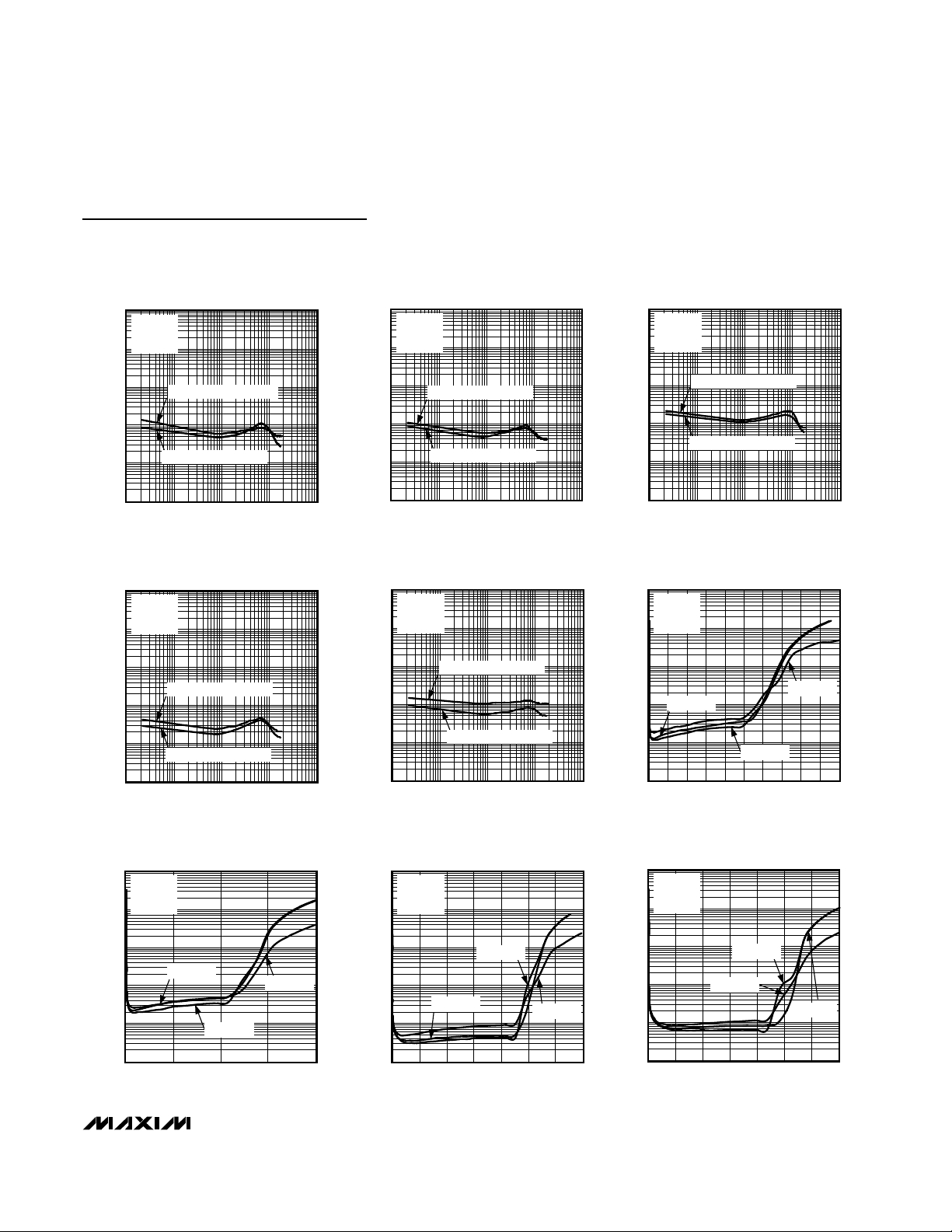
TOTAL HARMONIC DISTORTION PLUS NOISE
vs. FREQUENCY
MAX9718 toc01
FREQUENCY (Hz)
THD+N (%)
100 1k 10k
0.001
0.01
0.1
1
10
0.0001
10 100k
VCC = 5V
R
L
= 4
Ω
A
V
= 2
OUTPUT POWER = 1W
OUTPUT POWER = 50mW
TOTAL HARMONIC DISTORTION PLUS NOISE
vs. FREQUENCY
MAX9718 toc02
FREQUENCY (Hz)
THD+N (%)
100 1k 10k
0.001
0.01
0.1
1
10
0.0001
10 100k
VCC = 5V
R
L
= 4
Ω
A
V
= 4
OUTPUT POWER = 1W
OUTPUT POWER = 200mW
TOTAL HARMONIC DISTORTION PLUS NOISE
vs. FREQUENCY
MAX9718 toc03
FREQUENCY (Hz)
THD+N (%)
100 1k 10k
0.001
0.01
0.1
1
10
0.0001
10 100k
VCC = 5V
R
L
= 8
Ω
A
V
= 2
OUTPUT POWER = 250mW
OUTPUT POWER = 750mW
Typical Operating Characteristics
(VCC= 5V, C
BIAS
= 0.1µF, THD+N measurement bandwidth = 22Hz to 22kHz, TA= +25°C, unless otherwise noted.)
Note 1: All specifications are 100% tested at T
A
= +25°C. Specifications over temperature (TA= T
MIN
to T
MAX
) are guaranteed by
design, not production tested.
Note 2: Quiescent power-supply current is specified and tested with no load. Quiescent power-supply current depends on the offset
voltage when a practical load is connected to the amplifier. Guaranteed by design.
Note 3: Common-mode bias voltage is the voltage on BIAS and is nominally V
CC
/2.
Note 4: Output power is specified by a combination of a functional output current test and characterization analysis.
Note 5: Measurement bandwidth for THD+N is 22Hz to 22kHz.
Note 6: Peak voltage measured at power-on, power-off, into or out of SHDN. Bandwidth defined by A-weighted filters, inputs at AC
GND. V
CC
rise and fall times greater than or equal to 1ms.
MAX9718/MAX9719
Low-Cost, Mono/Stereo,
1.4W Differential Audio Power Amplifiers
4 _______________________________________________________________________________________
ELECTRICAL CHARACTERISTICS—3V Supply (continued)
(VCC= 3V, GND = 0, SHDN/SHDN = VCC(MAX9718/MAX9719), SHDM = GND (MAX9718), RIN= RF= 10kΩ (MAX971_A/H),
T
A
= +25°C. C
BIAS
= 0.1µF, no load. Typical values are at TA= +25°C, unless otherwise noted.) (Note 1)
PARAMETER SYMBOL CONDITIONS MIN TYP MAX UNITS
Output Power P
Total Harmonic Distortion Plus
Noise
Thermal-Shutdown Threshold +160 °C
Thermal-Shutdown Hysteresis 15 °C
Maximum Capacitive Drive C
Power-Up/Enable from
Shutdown Time
Shutdown Time t
Turn-Off Transient V
Crosstalk MAX9719, fN = 1kHz -85 dB
R
OUT
THD+N
LOAD
t
PU
SHDN
POP
= 8Ω, THD+N = 1%, f
L
R
L
A
V
= 8Ω, f
= 6dB
= 1kHz, P
IN
Bridge-tied capacitance 500 pF
(Note 6) 40 mV
= 1kHz (Note 4) 475 mW
IN
= 0.25W,
OUT
0.003 %
10 ms
3µs
MAX9718/MAX9719
Low-Cost, Mono/Stereo,
1.4W Differential Audio Power Amplifiers
_______________________________________________________________________________________ 5
Typical Operating Characteristics (continued)
(VCC= 5V, C
BIAS
= 0.1µF, THD+N measurement bandwidth = 22Hz to 22kHz, TA= +25°C, unless otherwise noted.)
TOTAL HARMONIC DISTORTION PLUS NOISE
vs. FREQUENCY
10
VCC = 5V
Ω
= 8
R
L
= 4
A
V
1
0.1
THD+N (%)
0.01
0.001
0.0001
10 100k
OUTPUT POWER = 800mW
OUTPUT POWER = 200mW
100 1k 10k
FREQUENCY (Hz)
TOTAL HARMONIC DISTORTION PLUS NOISE
vs. FREQUENCY
10
VCC = 3V
Ω
= 8
R
L
A
= 2
V
1
0.1
THD+N (%)
0.01
OUTPUT POWER = 100mW
TOTAL HARMONIC DISTORTION PLUS NOISE
vs. FREQUENCY
10
VCC = 3V
Ω
= 4
R
L
= 4
A
V
1
0.1
THD+N (%)
0.01
0.001
0.0001
10 100k
OUTPUT POWER = 175mW
OUTPUT POWER = 70mW
100 1k 10k
FREQUENCY (Hz)
TOTAL HARMONIC DISTORTION PLUS NOISE
vs. OUTPUT POWER
100
VCC = 5V
Ω
= 4
R
L
A
= 2
V
10
1
THD+N (%)
fIN = 100Hz
0.1
MAX9718 toc04
MAX9718 toc07
TOTAL HARMONIC DISTORTION PLUS NOISE
vs. FREQUENCY
10
VCC = 3V
Ω
= 4
R
L
= 2
A
V
1
0.1
THD+N (%)
0.01
0.001
0.0001
10 100k
OUTPUT POWER = 50mW
OUTPUT POWER = 250mW
100 1k 10k
FREQUENCY (Hz)
TOTAL HARMONIC DISTORTION PLUS NOISE
vs. FREQUENCY
10
VCC = 3V
Ω
= 8
R
L
A
= 4
V
1
0.1
THD+N (%)
0.01
OUTPUT POWER = 50mW
MAX9718 toc05
MAX9718 toc08
MAX9718 toc06
MAX9718 toc09
fIN = 10kHz
0.001
0.0001
OUTPUT POWER = 250mW
100 1k 10k
10 100k
FREQUENCY (Hz)
TOTAL HARMONIC DISTORTION PLUS NOISE
0.001
0.0001
10 100k
TOTAL HARMONIC DISTORTION PLUS NOISE
vs. OUTPUT POWER
100
VCC = 5V
Ω
= 4
R
L
A
= 4
V
10
1
THD+N (%)
0.1
0.01
0.001
02.0
fIN = 100Hz
fIN = 1kHz
0.5 1.51.0
OUTPUT POWER (W)
fIN = 10kHz
MAX9718 toc10
100
VCC = 5V
= 8
R
L
A
= 2
V
10
1
THD+N (%)
0.1
0.01
0.001
0.2 0.6 0.8 1.0 1.20.4
0 1.4
OUTPUT POWER = 200mW
100 1k 10k
FREQUENCY (Hz)
vs. OUTPUT POWER
Ω
fIN = 1kHz
fIN = 100Hz
OUTPUT POWER (W)
fIN = 10kHz
0.01
0.001
0.2 0.4 0.6 0.8 1.2 1.41.0 1.8
02.0
OUTPUT POWER (W)
TOTAL HARMONIC DISTORTION PLUS NOISE
vs. OUTPUT POWER
100
VCC = 5V
Ω
= 8
R
L
A
MAX9718 toc11
THD+N (%)
0.001
= 4
V
10
1
0.1
0.01
0.2 0.6 0.8 1.0 1.20.4
0 1.4
fIN = 100Hz
fIN = 1kHz
OUTPUT POWER (W)
fIN = 1kHz
1.6
MAX9718 toc12
fIN = 10kHz
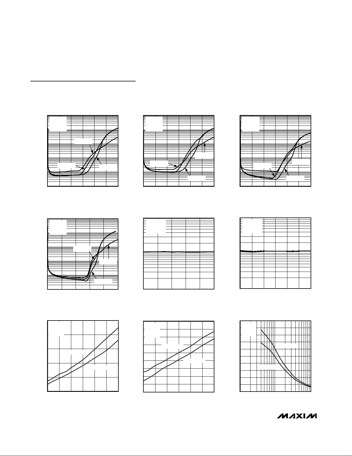
MAX9718/MAX9719
Low-Cost, Mono/Stereo,
1.4W Differential Audio Power Amplifiers
6 _______________________________________________________________________________________
Typical Operating Characteristics (continued)
(VCC= 5V, C
BIAS
= 0.1µF, THD+N measurement bandwidth = 22Hz to 22kHz, TA= +25°C, unless otherwise noted.)
TOTAL HARMONIC DISTORTION PLUS NOISE
vs. OUTPUT POWER
100
VCC = 3V
Ω
= 4
R
L
= 2
A
V
10
1
THD+N (%)
0.1
0.01
0.001
100 300 400 500200
0600
fIN = 10kHz
fIN = 1kHz
OUTPUT POWER (mW)
fIN = 100Hz
MAX9718 toc13
THD+N (%)
0.01
0.001
TOTAL HARMONIC DISTORTION PLUS NOISE
vs. OUTPUT POWER
100
VCC = 3V
Ω
= 8
R
L
A
10
1
THD+N (%)
0.1
= 4
V
fIN = 1kHz
fIN = 10kHz
MAX9718 toc16
0.001
THD+N (%)
TOTAL HARMONIC DISTORTION PLUS NOISE
vs. OUTPUT POWER
100
VCC = 3V
Ω
= 4
R
L
= 4
A
V
10
1
0.1
fIN = 1kHz
100 300 400 500200
0 600
OUTPUT POWER (mW)
fIN = 10kHz
fIN = 100Hz
TOTAL HARMONIC DISTORTION PLUS NOISE
vs. COMMON-MODE VOLTAGE
0.01
VCC = 5V
= 200mW
P
O
= 2
A
V
MAX9718 toc14
MAX9718 toc17
TOTAL HARMONIC DISTORTION PLUS NOISE
vs. OUTPUT POWER
100
VCC = 3V
Ω
= 8
R
L
= 2
A
V
10
1
THD+N (%)
0.1
fIN = 1kHz
0.01
0.001
100 300 400 500200
0600
OUTPUT POWER (mW)
fIN = 10kHz
fIN = 100Hz
MAX9718 toc15
TOTAL HARMONIC DISTORTION PLUS NOISE
vs. COMMON-MODE VOLTAGE
0.01
VCC = 3V
= 200mW
P
0.001
THD+N (%)
O
= 2
A
V
MAX9718 toc18
0.01
fIN = 100Hz
0.001
0
100 300 400 500200
OUTPUT POWER (mW)
OUTPUT POWER
vs. SUPPLY VOLTAGE
2.5
2.0
1.5
1.0
OUTPUT POWER
0.5
Ω
RL = 4
f = 1kHz
A
= 2
V
THD+N = 10%
THD+N = 1%
0
2.5 5.5
SUPPLY VOLTAGE (V)
0.0001
13452
0
COMMON-MODE VOLTAGE (V)
OUTPUT POWER
vs. SUPPLY VOLTAGE
1.8
1.6
MAX9718 toc19
1.4
1.2
1.0
0.8
0.6
OUTPUT POWER (W)
0.4
0.2
5.04.54.03.53.0
Ω
RL = 8
f = 1kHz
A
= 2
V
THD+N = 10%
THD+N = 1%
0
2.5 5.5
SUPPLY VOLTAGE (V)
5.04.54.03.53.0
0.0001
MAX9718 toc20
OUTPUT POWER (W)
0.5 1.5 2.0 2.5 3.01.0
0
COMMON-MODE VOLTAGE (V)
OUTPUT POWER
vs. LOAD RESISTANCE
2.0
VCC = 5V
1.8
f = 1kHz
= 2
A
V
1.6
1.4
1.2
1.0
0.8
0.6
0.4
0.2
0
1
THD+N = 1%
LOAD RESISTANCE (Ω)
MAX9718 toc21
THD+N = 10%
10010
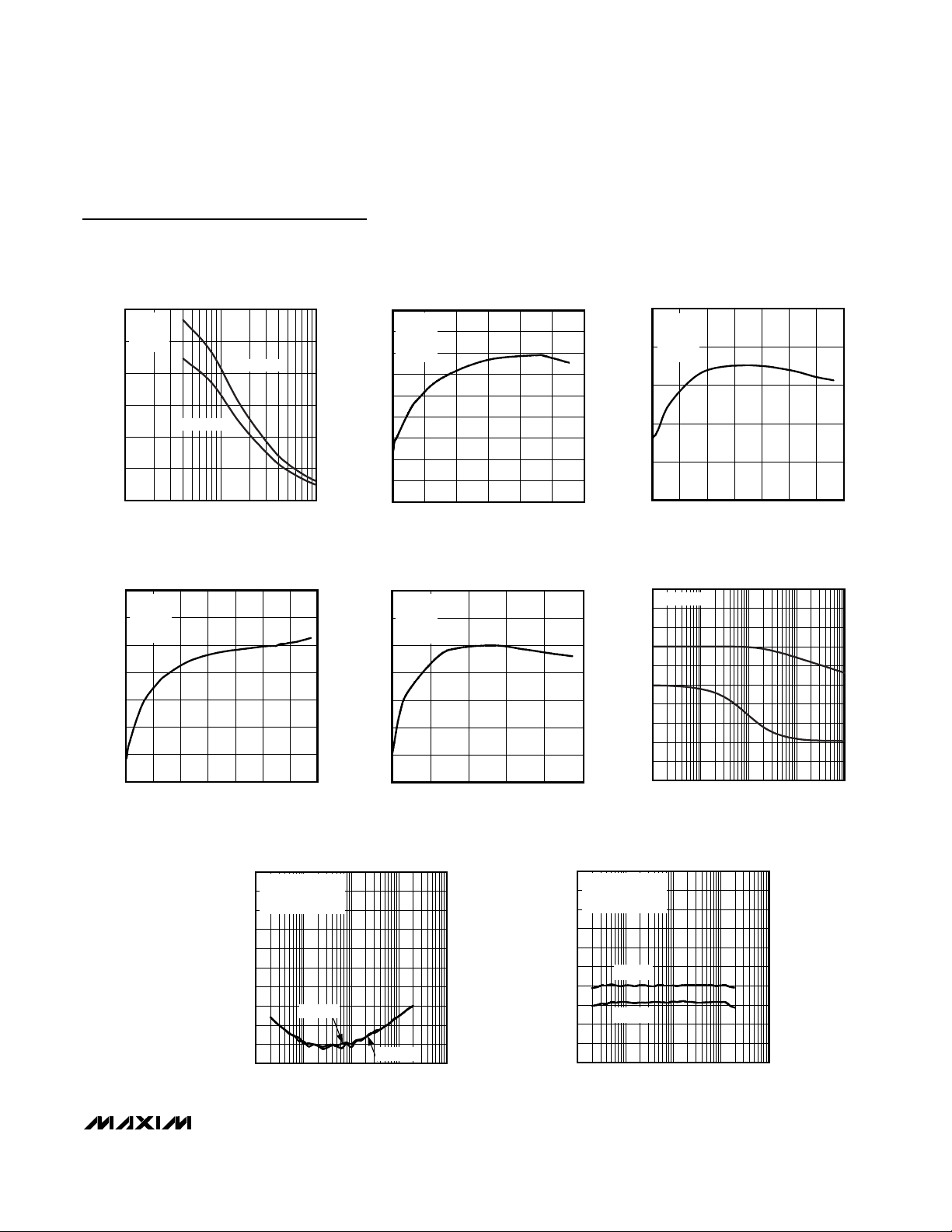
MAX9718/MAX9719
Low-Cost, Mono/Stereo,
1.4W Differential Audio Power Amplifiers
_______________________________________________________________________________________ 7
Typical Operating Characteristics (continued)
(VCC= 5V, C
BIAS
= 0.1µF, THD+N measurement bandwidth = 22Hz to 22kHz, TA= +25°C, unless otherwise noted.)
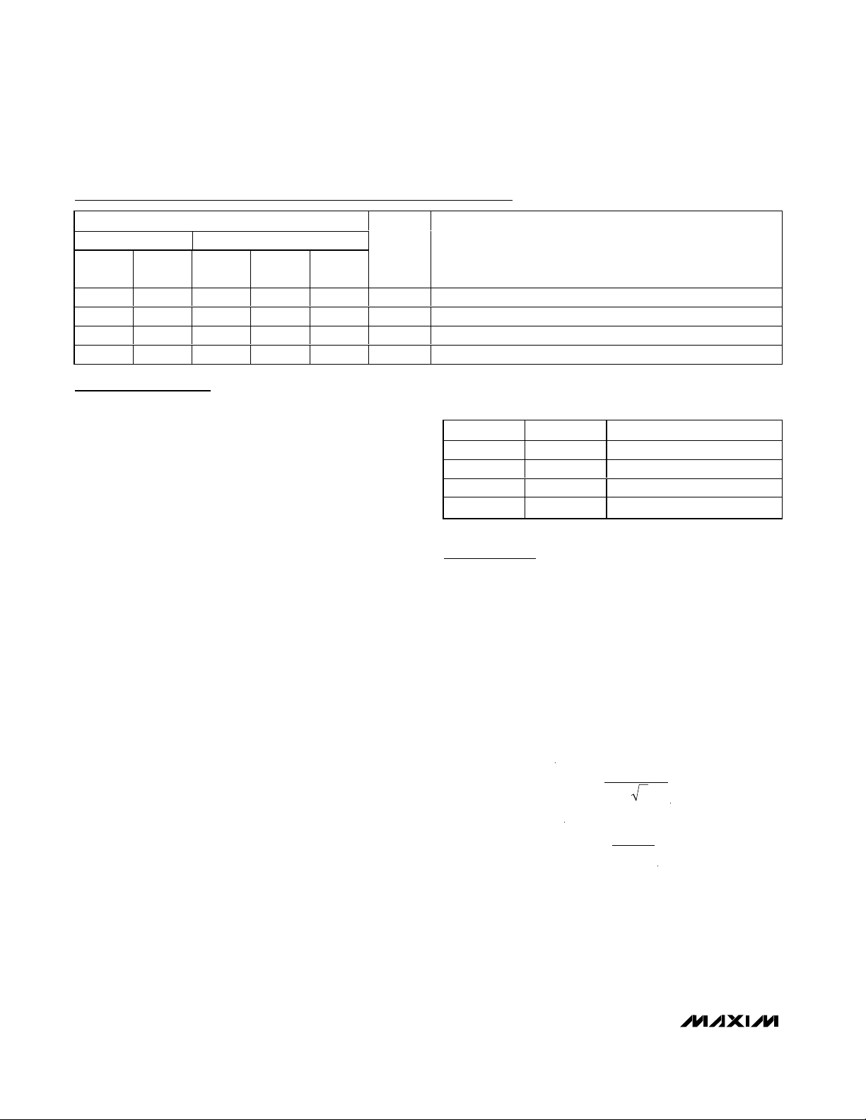
600
VCC = 3V
f = 1kHz
500
A
V
400
300
200
OUTPUT POWER (mW)
100
0
1
700
VCC = 3V
R
L
600
f = 1kHz
A
V
500
400
300
200
POWER DISSIPATION (mW)
100
0
0700
OUTPUT POWER
vs. LOAD RESISTANCE
1.8
VCC = 5V
= 4
R
1.6
L
= 2
THD+N = 1%
LOAD RESISTANCE (Ω)
MAX9718 toc22
THD+N = 10%
10010
f = 1kHz
1.4
= 2
A
V
1.2
1.0
0.8
0.6
POWER DISSIPATION (W)
0.4
0.2
0
0 1.8
POWER DISSIPATION
vs. OUTPUT POWER
350
Ω
= 4
= 2
OUTPUT POWER (mW)
MAX9718 toc25
600500400300200100
VCC = 3V
= 8
R
L
300
f = 1kHz
= 2
A
V
250
200
150
100
POWER DISSIPATION (mW)
50
0
0 500
POWER DISSIPATION
vs. OUTPUT POWER
Ω
OUTPUT POWER (W)
POWER DISSIPATION
vs. OUTPUT POWER
Ω
OUTPUT POWER (mW)
POWER DISSIPATION
1.0
MAX9718 toc23
0.8
0.6
0.4
POWER DISSIPATION (W)
0.2
0
1.51.20.90.60.3
MAX9718 toc26
400300200100
01.4
150
120
90
60
30
0
-30
GAIN/PHASE (°/dB)
-60
-90
-120
-150
10 100k
vs. OUTPUT POWER
VCC = 5V
Ω
= 8
R
L
f = 1kHz
= 2
A
V
GAIN AND PHASE
AV = 60dB
MAX9718 toc24
1.21.00.80.60.40.2
OUTPUT POWER (W)
vs. FREQUENCY
MAX9718 toc27
10k1k100
FREQUENCY (Hz)
POWER-SUPPLY REJECTION RATIO
vs. FREQUENCY
0
V
= 200mV
RIPPLE
-10
RL = 8
C
BIAS
-20
-30
-40
-50
PSRR (dB)
-60
-70
-80
-90
-100
10 100k
Ω
= 1μF
VCC = 5V
P-P
VCC = 3V
FREQUENCY (Hz)
MAX9718 toc28
10k1k100
COMMON-MODE REJECTION RATIO
vs. FREQUENCY
0
V
= 200mV
RIPPLE
-10
RL = 8
C
BIAS
-20
-30
-40
-50
CMRR (dB)
-60
-70
-80
-90
-100
10 100k
Ω
= 1μF
VCC = 5V
VCC = 3V
P-P
FREQUENCY (Hz)
MAX9718 toc29
10k1k100

MAX9718/MAX9719
Low-Cost, Mono/Stereo,
1.4W Differential Audio Power Amplifiers
8 _______________________________________________________________________________________
Typical Operating Characteristics (continued)
(VCC= 5V, C
BIAS
= 0.1µF, THD+N measurement bandwidth = 22Hz to 22kHz, TA= +25°C, unless otherwise noted.)
CROSSTALK
vs. FREQUENCY
MAX9718 toc31
FREQUENCY (Hz)
CROSSTALK (dB)
10k1k100
-90
-80
-70
-60
-50
-40
-30
-20
-10
0
-100
-110
-120
10 100k
CHANNEL 2
CHANNEL 1
VCC = 3V
V
RIPPLE
= 200mV
P-P
RL = 8
Ω
C
BIAS
= 1μF
ENTERING SHUTDOWN
MAX9718 toc32
100μs/div
C
BIAS
= 0.1μF
V
CC
= 3V
R
L
= 8Ω
SHDN
2V/div
OUT+
1V/div
OUT1V/div
OUT+ - OUT200mV/div
EXITING SHUTDOWN
MAX9718 toc33
4ms/div
C
BIAS
= 0.1μF
V
CC
= 3V
R
L
= 8Ω
SHDN
2V/div
OUT+
1V/div
OUT1V/div
OUT+ - OUT200mV/div
ENTERING POWER-DOWN
MAX9718 toc34
100μs/div
C
BIAS
= 0.1μF
V
CC
= 3V
R
L
= 8Ω
SHDN
1V/div
OUT+
1V/div
OUT1V/div
OUT+ - OUT200mV/div
EXITING POWER-DOWN
MAX9718 toc35
SHDN
2V/div
OUT+
1V/div
OUT1V/div
4ms/div
C
BIAS
= 0.1μF
V
CC
= 3V
R
L
= 8Ω
OUT+ - OUT200mV/div
CROSSTALK
vs. FREQUENCY
MAX9718 toc30
FREQUENCY (Hz)
CROSSTALK (dB)
10k1k100
-90
-80
-70
-60
-50
-40
-30
-20
-10
0
-100
-110
-120
10 100k
CHANNEL 2
CHANNEL 1
VCC = 5V
V
RIPPLE
= 200mV
P-P
RL = 8Ω,
C
BIAS
= 1μF

MAX9718/MAX9719
Low-Cost, Mono/Stereo,
1.4W Differential Audio Power Amplifiers
_______________________________________________________________________________________ 9
Typical Operating Characteristics (continued)
(VCC= 5V, C
BIAS
= 0.1µF, THD+N measurement bandwidth = 22Hz to 22kHz, TA= +25°C, unless otherwise noted.)
Pin Description
6
5
4
3
2
SUPPLY CURRENT (mA)
1
0
-40 85
MAX9718 MAX9719
TDFN/
µMAX
1 C2 — — — SHDN
—— 9 B311SHDN Shutdown Input. Active-low shutdown input.
2 C1 — — — IN- Inverting Input
3 B2 — — — SHDM
4 A1 — — — IN+ Noninverting Input
5 A2 5 B2 7 BIAS DC Bias Bypass
6 A3 — — — OUT- Bridge Amplifier Negative Output
7 B3 1, 6, 11
8 — 13 — 15 N.C. No Connection. Not internally connected.
9 B1 8, 14 A4, D3 16, 10 V
10 C3 — — — OUT+ Bridge Amplifier Positive Output
— — 2 C1 4 INR+ Right-Channel Noninverting Input
— — 3 B1 5 INL- Left-Channel Inverting Input
— — 4 A1 6 INL+ Left-Channel Noninverting Input
— — 7 A3 9 OUTL+ Left-Channel Bridge Amplifier Positive Output
— — 10 B4 12 OUTL- Left-Channel Bridge Amplifier Negative Output
SUPPLY CURRENT
vs. TEMPERATURE
VCC = 5V
VCC = 3V
TEMPERATURE (°C)
0.03
0.02
MAX9718 toc36
0.01
0
-0.01
SHUTDOWN CURRENT (μA)
-0.02
-0.03
603510-15
-40 85
SHUTDOWN CURRENT
vs. TEMPERATURE
VCC = 5V
TEMPERATURE (°C)
VCC = 3V
603510-15
MAX9718 toc37
TURN-ON TIME (ms)
vs. DC BIAS BYPASS CAPACITOR
80
TO -3dB OF FINAL VALUE
70
60
50
40
30
20
10
0
0 1.00
PIN
NAME FUNCTION
UCSP TQFN UCSP TSSOP
Shutdown Input. The polarity of SHDN is dependent on the state
of SHDM.
Shutdown-Mode Polarity Input. SHDM controls the polarity of
SHDN. Connect SHDM high for an active-high SHDN input.
Connect SHDM low for an active-low SHDN input (see Table 1).
A2,
C2, C4
3, 8,13 GND Ground
Power Supply
CC
TURN-ON TIME
VCC = 5V
VCC = 3V
0.800.600.20 0.40
C
(μF)
BIAS
MAX9718 toc38
MAX9718/MAX9719
Low-Cost, Mono/Stereo,
1.4W Differential Audio Power Amplifiers
10 ______________________________________________________________________________________
Pin Description (continued)
Detailed Description
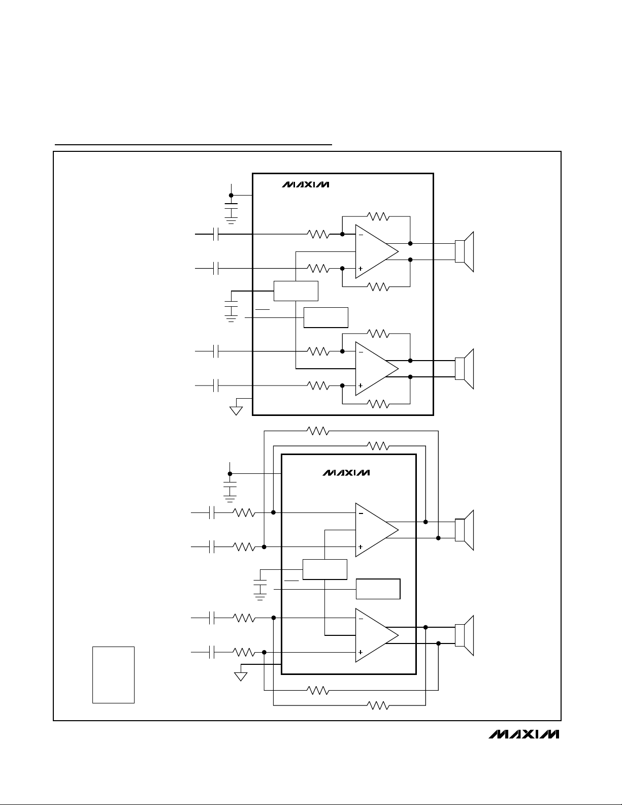
The MAX9718/MAX9719 are 1.4W BTL speaker amplifiers. The MAX9718 is a mono speaker amplifier, while
the MAX9719 is a stereo speaker amplifier. Both
devices feature a low-power shutdown mode, and
industry-leading click-and-pop suppression. The
MAX9718 features a two-input shutdown scheme to
configure shutdown for active high or active low. These
devices consist of high output-current audio amps configured as BTL amplifiers (see the Functional Diagrams).
Both adjustable and fixed gain (0dB, 3dB, 6dB) versions
are available.
BIAS
These devices operate from a single 2.7V to 5.5V supply and feature an internally generated, common-mode
bias voltage of VCC/ 2 referenced to ground. BIAS provides both click-and-pop suppression and sets the DC
bias level for the audio outputs. Choose the value of the
bypass capacitor as described in the BIAS Capacitor
section. Do not connect external loads to BIAS as this
can affect the overall performance.
Shutdown Mode
The MAX9718/MAX9719 feature a 100nA low-power
shutdown mode that reduces quiescent current consumption. Entering shutdown disables the device’s bias
circuitry, the amplifier outputs go high impedance, and
BIAS is driven to GND. The MAX9718 SHDM input controls the polarity of SHDN. Drive SHDM high for an
active-high SHDN input. Drive SHDM low for an activelow SHDN input (see Table 1). The MAX9719 features
an active-low shutdown input, SHDN.
Click-and-Pop Suppression
The MAX9718/MAX9719 feature Maxim’s industry-leading click-and-pop suppression circuitry. During startup,
the amplifier common-mode bias voltage ramps to the
DC bias point. When entering shutdown, the amplifier
outputs are high impedance to 100kΩ between both
outputs. This scheme minimizes the energy present in
the audio band.
Applications Information
BTL Amplifier
The MAX9718/MAX9719 are designed to drive a load
differentially, a configuration referred to as bridge-tied
load or BTL. The BTL configuration (Figure 1) offers
advantages over the single-ended configuration, where
one side of the load is connected to ground. Driving the
load differentially doubles the output voltage compared
to a single-ended amplifier under similar conditions.
Substituting 2 x V
OUT(P-P)
for V
OUT(P-P)
into the following
equations yields four times the output power due to
doubling of the output voltage:
Since the differential outputs are biased at midsupply,
there is no net DC voltage across the load. This eliminates the need for DC-blocking capacitors required for
single-ended amplifiers. These capacitors can be
large, expensive, consume board space, and degrade
low-frequency performance.
P
V
R
OUT
RMS
L
=
2
V
V
RMS
OUT P P
=
−()
22
Table 1. Shutdown Mode Selection
(MAX9718 Only)
PIN
MAX9718 MAX9719
TDFN/
µMAX
— — 12 D4 14 OUTR+ Right-Channel Bridge Amplifier Positive Output
— — 15 D2 1 OUTR- Right-Channel Bridge Amplifier Negative Output
— — 16 D1 2 INR- Right-Channel Inverting Input
EP — EP — EP EP Exposed Pad. Connect EP to GND.
UCSP TQFN UCSP TSSOP
NAME FUNCTION
SHDM SHDN OPERATIONAL MODE
0 0 Shutdown
0 1 Normal operation
1 0 Normal operation
1 1 Shutdown

Power Dissipation and Heat Sinking
Under normal operating conditions, the MAX9718/
MAX9719 dissipate a significant amount of power. The
maximum power dissipation for each package is given
in the Absolute Maximum Ratings section under
Continuous Power Dissipation or can be calculated by
the following equation:
where T
J(MAX)
is +150°C, TAis the ambient tempera-
ture, and θJAis the reciprocal of the derating factor in
°C/W as specified in the Absolute Maximum Ratings
section. For example, θJAof the TQFN package is
+59.2°C/W.
The increase in power delivered by the BTL configuration directly results in an increase in internal power dissipation over the single-ended configuration. The
maximum internal power dissipation for a given V
CC
and load is given by the following equation:
If the internal power dissipation for a given application
exceeds the maximum allowed for a given package,
reduce power dissipation by increasing the ground
plane heat-sinking capability and the size of the traces
to the device (see the Layout and Grounding section).
Other methods for reducing power dissipation are to
reduce V
CC
, increase load impedance, decrease ambi-
ent temperature, reduce gain, or reduce input signal.
Thermal-overload protection limits total power dissipation in the MAX9718/MAX9719. When the junction temperature exceeds +160°C, the thermal protection
circuitry disables the amplifier output stage. The amplifiers are enabled once the junction temperature cools
by 15°C. A pulsing output under continuous thermal
overload results as the device heats and cools.
For optimum power dissipation and heat sinking, connect the exposed pad found on the µMAX, TDFN,
TQFN, and TSSOP packages to a large ground plane.
Fixed Differential Gain
The MAX9718B/E, MAX9718C/F, MAX9718D/G,
MAX9719B, MAX9719C, and MAX9719D feature internally fixed gains (see the Selector Guide). This simplifies design, decreases required footprint size, and
eliminates external gain-setting resistors. Resistors R1
and R2 shown in the Typical Operating Circuit are used
to achieve each fixed gain.
Adjustable Differential Gain
Gain-Setting Resistors
External feedback resistors set the gain of the
MAX9718A/H and MAX9719A. Resistors RFand R
IN
(Figure 2) set the gain of the amplifier as follows:
where AVis the desired voltage gain. Hence, an RINof
10kΩ and an RFof 20kΩ yields a gain of 2V/V, or 6dB.
RFcan be either fixed or variable, allowing the use of a
digitally controlled potentiometer to alter the gain under
software control.
A
R
R
V
F
IN
=
P
V
R
D MAX
CC
()
=
2
2
2
π
P
TT
D MAX
J MAX A
JA
()
()
=
−
θ
MAX9718/MAX9719
Low-Cost, Mono/Stereo,
1.4W Differential Audio Power Amplifiers
______________________________________________________________________________________ 11
Figure 1. Bridge-Tied Load Configuration
Figure 2. Setting the MAX9718A/H/MAX9719A Gain
+1
-1
V
OUT(P-P)
2 x V
V
OUT(P-P)
OUT(P-P)
R
F
R
F
MAX9718A/H
R
INVERTING
DIFFERENTIAL
INPUT
(OPTIONAL)
NONINVERTING
DIFFERENTIAL
INPUT
(OPTIONAL)
IN
R
IN
MAX9719A
IN-
OUT+
OUT-
GENERATOR
IN+
BIAS
MAX9718/MAX9719
Input Filter
The fully differential amplifier inputs can be biased at
voltages other than midsupply. The common-mode
feedback circuit adjusts for input bias, ensuring the
outputs are still biased at midsupply. Input capacitors
are not required as long as the common-mode input
voltage is within the specified range listed in the
Electrical Characteristics table.
If input capacitors are used, input capacitor CIN, in
conjunction with RIN, forms a highpass filter that
removes the DC bias from an incoming signal. The ACcoupling capacitor allows the amplifier to bias the signal to an optimum DC level. Assuming zero-source
impedance, the -3dB point of the highpass filter is
given by:
Setting f
-3dB
too high affects the low-frequency
response of the amplifier. Use capacitors with
dielectrics that have low-voltage coefficients, such as
tantalum or aluminum electrolytic. Capacitors with highvoltage coefficients, such as ceramics, can increase
distortion at low frequencies.
BIAS Capacitor
BIAS is the output of the internally generated V
CC
/2
bias voltage. The BIAS bypass capacitor, C
BIAS
,
improves PSRR and THD+N by reducing power supply
and other noise sources at the common-mode bias
node, and also generates the clickless/popless startup
DC bias waveform for the speaker amplifiers. Bypass
BIAS with a 0.1µF capacitor to GND. Larger values of
C
BIAS
(up to 1µF) improve PSRR, but slow down
tON/t
OFF
times. A 1µF C
BIAS
capacitor slows turn-on
and turn-off times by 10 and improves PSRR by 20dB
(at 1kHz). Do not connect external loads to BIAS.
Supply Bypassing
Proper power-supply bypassing ensures low-noise,
low-distortion performance. Connect a 1µF ceramic
capacitor from VCCto GND. Add additional bulk
capacitance as required by the application. Locate the
bypass capacitor as close to the device as possible.
Layout and Grounding
Good PC board layout is essential for optimizing performance. Use large traces for the power-supply inputs and
amplifier outputs to minimize losses due to parasitic trace
resistance and route heat away from the device. Good
grounding improves audio performance, minimizes
crosstalk between channels, and prevents any digital
switching noise from coupling into the audio signal.
The MAX9718/MAX9719 TDFN, TQFN, TSSOP, and
µMAX packages feature exposed thermal pads on their
undersides. This pad lowers the thermal resistance of the
package by providing a direct-heat conduction path
from the die to the PC board. Connect the exposed pad
to the ground plane using multiple vias, if required.
UCSP Applications Information
For the latest application details on UCSP construction,
dimensions, tape carrier information, PC board techniques, bump-pad layout, and recommended reflow
temperature profile, as well as the latest information on
reliability testing results, refer to the Application Note:
UCSP—A Wafer-Level Chip-Scale Package available
on Maxim’s website at www.maxim-ic.com/ucsp.
f
RC
dB
IN IN
−
=
3
1
2π
Low-Cost, Mono/Stereo,
1.4W Differential Audio Power Amplifiers
12 ______________________________________________________________________________________
Selector Guide
PART MONO STEREO
MAX9718A/H √ — Adjustable √
MAX9718B/E √ —0 √
MAX9718C/F √ —3 √
MAX9718D/G √ —6 √
MAX9719A — √ Adjustable —
MAX9719B — √ 0—
MAX9719C — √ 3—
MAX9719D — √ 6—
GAIN
(dB)
SELECTABLE
SHUTDOWN
POLARITY
MAX9718/MAX9719
Low-Cost, Mono/Stereo,
1.4W Differential Audio Power Amplifiers
______________________________________________________________________________________ 13
Ordering Information (continued)
Chip Information
MAX9718 TRANSISTOR COUNT: 2359
MAX9719 TRANSISTOR COUNT: 4447
PROCESS: BiCMOS
UCSP Marking Information:
■: A1 Bump indicator
AAA: Product code
XXX: Lot code
+Denotes lead-free package.
*EP = Exposed paddle.
PART TEMP RANGE
MAX9718AETB+T -40°C to +85°C 10 TDFN-EP* +AAV
MAX9718AEUB -40°C to +85°C 10 µMAX-EP* AAAA
MAX9718AEUB+ -40°C to +85°C 10 µMAX-EP* +AAAA
MAX9718BEBL-T -40°C to +85°C 3 x 3 UCSP ADY
MAX9718BEBL+T -40°C to +85°C 3 x 3 UCSP +ADY
MAX9718BETB-T -40°C to +85°C 10 TDFN-EP* AAW
MAX9718BETB+T -40°C to +85°C 10 TDFN-EP* +AAW
MAX9718BEUB -40°C to +85°C 10 µMAX-EP* AAAB
MAX9718BEUB+ -40°C to +85°C 10 µMAX-EP* +AAAB
MAX9718CEBL-T -40°C to +85°C 3 x 3 UCSP ADZ
MAX9718CEBL+T -40°C to +85°C 3 x 3 UCSP +ADZ
MAX9718CETB-T -40°C to +85°C 10 TDFN-EP* AAX
MAX9718CETB+T -40°C to +85°C 10 TDFN-EP* +AAX
MAX9718CEUB -40°C to +85°C 10 µMAX-EP* AAAC
MAX9718CEUB+ -40°C to +85°C 10 µMAX-EP* +AAAC
MAX9718DEBL-T -40°C to +85°C 3 x 3 UCSP AEA
MAX9718DEBL+T -40°C to +85°C 3 x 3 UCSP +AEA
MAX9718DETB-T -40°C to +85°C 10 TDFN-EP* AAY
MAX9718DETB+T -40°C to +85°C 10 TDFN-EP* +AAY
MAX9718DEUB -40°C to +85°C 10 µMAX-EP* AAAD
MAX9718DEUB+ -40°C to +85°C 10 µMAX-EP* +AAAD
MAX9718EEBL+T -40°C to +85°C 3 x 3 UCSP +AFB
MAX9718EETB+T -40°C to +85°C 10 TDFN-EP* +ASY
MAX9718EEUB+ -40°C to +85°C 10 µMAX-EP* +AAAJ
MAX9718FEBL+T -40°C to +85°C 3 x 3 UCSP +AFC
MAX9718FETB+T -40°C to +85°C 10 TDFN-EP* +ASZ
MAX9718FEUB+ -40°C to +85°C 10 µMAX-EP* +AAAK
MAX9718GEBL+T -40°C to +85°C 3 x 3 UCSP +AFD
MAX9718GETB+T -40°C to +85°C 10 TDFN-EP* +ATA
MAX9718GEUB+ -40°C to +85°C 10 µMAX-EP* +AAAL
MAX9718HEBL+T -40°C to +85°C 3 x 3 UCSP +AFE
MAX9718HETB+T -40°C to +85°C 10 TDFN-EP* +ATB
MAX9718HEUB+ -40°C to +85°C 10 µMAX-EP* +AAAM
MAX9719AEBE-T -40°C to +85°C 4 x 4 UCSP —
MAX9719AEBE+T -40°C to +85°C 4 x 4 UCSP —
PINPACKAGE
TOP
MARK
PART TEMP RANGE
MAX9719AETE -40°C to +85°C 16 TQFN-EP* —
MAX9719AETE+ -40°C to +85°C 16 TQFN-EP* —
MAX9719AEUE -40°C to +85°C 16 TSSOP-EP* —
MAX9719AEUE+ -40°C to +85°C 16 TSSOP-EP* —
MAX9719BEBE-T -40°C to +85°C 4 x 4 UCSP —
MAX9719BEBE+T -40°C to +85°C 4 x 4 UCSP —
MAX9719BETE -40°C to +85°C 16 TQFN-EP* —
MAX9719BETE+ -40°C to +85°C 16 TQFN-EP* —
MAX9719BEUE -40°C to +85°C 16 TSSOP-EP* —
MAX9719BEUE+ -40°C to +85°C 16 TSSOP-EP* —
MAX9719CEBE-T -40°C to +85°C 4 x 4 UCSP —
MAX9719CEBE+T -40°C to +85°C 4 x 4 UCSP —
MAX9719CETE -40°C to +85°C 16 TQFN-EP* —
MAX9719CETE+ -40°C to +85°C 16 TQFN-EP* —
MAX9719CEUE -40°C to +85°C 16 TSSOP-EP* —
MAX9719CEUE+ -40°C to +85°C 16 TSSOP-EP* —
MAX9719DEBE-T -40°C to +85°C 4 x 4 UCSP —
MAX9719DEBE+T -40°C to +85°C 4 x 4 UCSP —
MAX9719DETE -40°C to +85°C 16 TQFN-EP* —
MAX9719DETE+ -40°C to +85°C 16 TQFN-EP* —
MAX9719DEUE -40°C to +85°C 16 TSSOP-EP* —
MAX9719DEUE+ -40°C to +85°C 16 TSSOP-EP* —
AAA
XXX
PINPACKAGE
TOP
MARK

MAX9718/MAX9719
Low-Cost, Mono/Stereo,
1.4W Differential Audio Power Amplifiers
14 ______________________________________________________________________________________
System Diagram
2.7V TO 5.5V
10μF
1μF
IN1+
IN1-
IN2+
IN2-
1μF
V
CC
INL+
INL-
INR+
INR-
GND
SHDN
Q
Q
SHDN
INL
MAX9719
MAX961
MAX9722B
OUTL+
OUTL-
OUTR+
OUTR-
BIAS
V
OUTL
IN-
IN+
0.1μF
CC
0.1μF 0.1μF
2.7V TO 5.5V
220kΩ
2.7V TO 5.5V
1μF
INR
PV
DD
SV
DD
C1P CIN
AUTOMATIC HEADPHONE DETECTION AND SPEAKER DISABLE CIRCUIT
1μF
OUTR
PV
SV
SS
SS
1μF0.1μF1μF

MAX9718/MAX9719
Low-Cost, Mono/Stereo,
1.4W Differential Audio Power Amplifiers
______________________________________________________________________________________ 15
Functional Diagrams
2.7V TO 5.5V
SUPPLY
V
CC
IN-
IN+
BIAS
SHDN
SHDM
GND
BIAS
GENERATOR
SHUTDOWN
CONTROL
R
2
R
1
OUT+
R
1
R
2
OUT-
MAX9718B/E
MAX9718C/F
MAX9718D/G
INVERTING
DIFFERENTIAL
INPUT
NONINVERTING
DIFFERENTIAL
INPUT
1.0μF
C
IN
(OPTIONAL)
C
IN
(OPTIONAL)
C
BIAS
0.1μF
INVERTING
DIFFERENTIAL
INPUT
NONINVERTING
DIFFERENTIAL
INPUT
MAX9718A
= 2
A
V
= 1Hz
f
C
= 1μF
C
IN
= 10kΩ
R
IN
= 20kΩ
R
F
2.7V TO 5.5V
1.0μF
C
IN
(OPTIONAL)
C
IN
(OPTIONAL)
SUPPLY
R
IN
R
IN
C
BIAS
0.1μF
V
CC
IN-
IN+
BIAS
SHDN
SHDM
GND
R
F
BIAS
GENERATOR
SHUTDOWN
CONTROL
R
F
MAX9718A/H
OUT+
OUT-
MAX9718/MAX9719
Low-Cost, Mono/Stereo,
1.4W Differential Audio Power Amplifiers
16 ______________________________________________________________________________________
Functional Diagrams (continued)
2.7V TO 5.5V
SUPPLY
1.0μF
C
INVERTING
DIFFERENTIAL
INPUT
NONINVERTING
DIFFERENTIAL
INPUT
INVERTING
DIFFERENTIAL
INPUT
NONINVERTING
DIFFERENTIAL
INPUT
IN
(OPTIONAL)
C
IN
(OPTIONAL)
C
BIAS
0.1μF
C
IN
(OPTIONAL)
C
IN
(OPTIONAL)
V
CC
INL-
INL+
BIAS
SHDN
INR-
INR+
GND
MAX9719B
MAX9719C
MAX9719D
BIAS
GENERATOR
R
1
R
1
SHUTDOWN
CONTROL
R
1
R
1
R
2
OUTL+
OUTL-
R
2
R
2
OUTR+
OUTR-
R
2
MAX9719A
= 2
A
V
= 1Hz
f
C
= 1μF
C
IN
= 10kΩ
R
IN
= 20kΩ
R
F
INVERTING
DIFFERENTIAL
INPUT
NONINVERTING
DIFFERENTIAL
INPUT
INVERTING
DIFFERENTIAL
INPUT
NONINVERTING
DIFFERENTIAL
INPUT
2.7V TO 5.5V
1.0μF
C
IN
(OPTIONAL)
C
IN
(OPTIONAL)
C
IN
(OPTIONAL)
C
IN
(OPTIONAL)
SUPPLY
R
IN
R
IN
C
BIAS
0.1μF
R
IN
R
IN
V
CC
INL-
INL+
BIAS
SHDN
INR-
INR+
GND
R
F
MAX9719A
BIAS
GENERATOR
R
F
R
F
SHUTDOWN
CONTROL
R
F
OUTL+
OUTL-
OUTR+
OUTR-

MAX9718/MAX9719
Low-Cost, Mono/Stereo,
1.4W Differential Audio Power Amplifiers
______________________________________________________________________________________ 17
Pin Configurations
TOP VIEW TOP VIEW
(BUMPS ON BOTTOM)
SHDN
SHDM
1
IN-
2
3
MAX9718
4
5
10
OUT+
9
V
CC
N.C.
8
GNDIN+
7
OUT-BIAS
6
μMAX 3 × 3 UCSP
TOP VIEW
TOP VIEW
(BUMPS ON BOTTOM)
SHDN
SHDM
1
2
IN-
3
MAX9718
4
5
10
OUT+
9
V
CC
8
N.C.
7
GNDIN+
OUT-BIAS
6
TDFN
(3mm × 3mm × 0.8mm)
BIAS
SHDM
SHDN
MAX9718
OUTL+
SHDN
V
CC
OUT-
OUT+
123
IN+
A
V
B
CC
IN-
C
1234
GND
INL+
A
BIAS
INL-
B
GND GND
INR+
C
INR-
D
OUTR-
GND
MAX9719
OUTL-
OUTR+
V
CC
TOP VIEW TOP VIEW
OUTR+
GND
OUTL-
SHDN
12
11 10 9
N.C.
V
13
14
CC
V
8
CC
OUTL+
7
MAX9719
OUTR-
INR-
15
16
1234
GND
INR+
INL-
INL+
GND
6
BIAS
5
TQFN
(4mm × 4mm × 0.8mm)
OUTR-
INR-
GND
INR+
INL-
INL+
BIAS
GND
1
2
3
4
5
6
7
8
4 × 4 UCSP
MAX9719
TSSOP-EP
16
V
CC
15
N.C.
14
OUTR+
13
GND
12
OUTL-
SHDN
11
10
V
CC
OUTL+
9

MAX9718/MAX9719
Low-Cost, Mono/Stereo,
1.4W Differential Audio Power Amplifiers
18 ______________________________________________________________________________________
Package Information
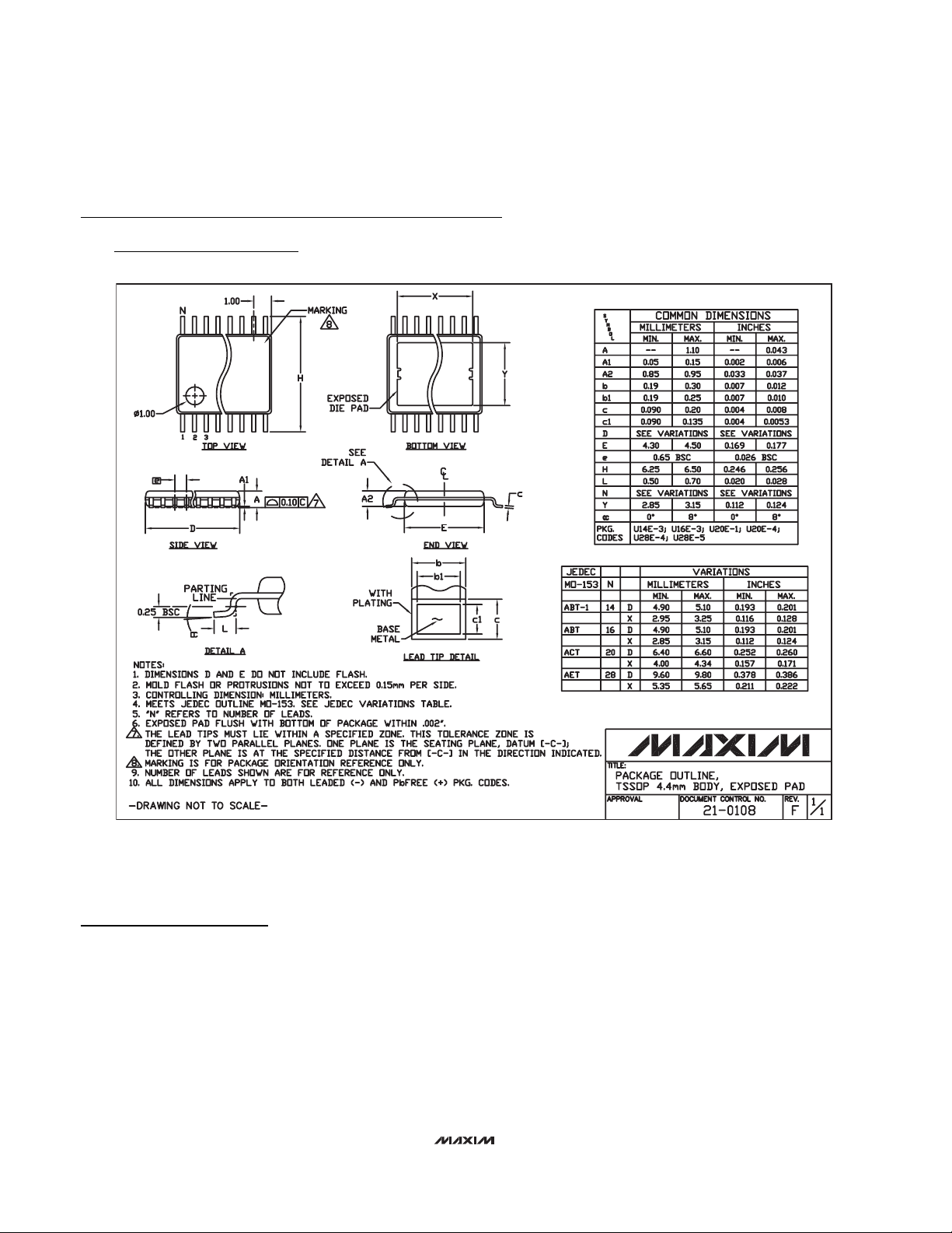
(The package drawing(s) in this data sheet may not reflect the most current specifications. For the latest package outline information
go to www.maxim-ic.com/packages
.)
9LUCSP, 3x3.EPS
PACKAGE OUTLINE, 3x3 UCSP
21-0093
1
L
1

MAX9718/MAX9719
Low-Cost, Mono/Stereo,
1.4W Differential Audio Power Amplifiers
______________________________________________________________________________________ 19
Package Information (continued)
(The package drawing(s) in this data sheet may not reflect the most current specifications. For the latest package outline information
go to www.maxim-ic.com/packages
.)
6, 8, &10L, DFN THIN.EPS
COMMON DIMENSIONS
SYMBOL MIN. MAX.
A 0.70 0.80
D 2.90 3.10
E 2.90 3.10
A1
0.00 0.05
L 0.20 0.40
0.25 MIN.k
A2 0.20 REF.
PACKAGE VARIATIONS
PKG. CODE N D2 E2 e JEDEC SPEC b
T633-2 6 1.50±0.10 2.30±0.10 0.95 BSC MO229 / WEEA 0.40±0.05 1.90 REF
T833-2 8 1.50±0.10 2.30±0.10 0.65 BSC MO229 / WEEC 0.30±0.05 1.95 REF
T833-3 8 1.50±0.10 2.30±0.10 0.65 BSC MO229 / WEEC 0.30±0.05 1.95 REF
1.50±0.10 MO229 / WEED-3
2.30±0.10 MO229 / WEED-3 2.00 REF0.25±0.050.50 BSC1.50±0.1010T1033-2
0.40 BSC - - - - 0.20±0.05 2.40 REFT1433-2 14 2.30±0.101.70±0.10
[(N/2)-1] x e
2.00 REF0.25±0.050.50 BSC2.30±0.1010T1033-1
2.40 REF0.20±0.05- - - - 0.40 BSC1.70±0.10 2.30±0.1014T1433-1

MAX9718/MAX9719
Low-Cost, Mono/Stereo,
1.4W Differential Audio Power Amplifiers
20 ______________________________________________________________________________________
Package Information (continued)
(The package drawing(s) in this data sheet may not reflect the most current specifications. For the latest package outline information
go to www.maxim-ic.com/packages
.)
10L UMAX, EXPPADS.EPS
21-0109
1
D
1

MAX9718/MAX9719
Low-Cost, Mono/Stereo,
1.4W Differential Audio Power Amplifiers
______________________________________________________________________________________ 21
Package Information (continued)
(The package drawing(s) in this data sheet may not reflect the most current specifications. For the latest package outline information
go to www.maxim-ic.com/packages
.)
16L,UCSP.EPS
PACKAGE OUTLINE, 4x4 UCSP
21-0101
1
H
1
MAX9718/MAX9719
Low-Cost, Mono/Stereo,
1.4W Differential Audio Power Amplifiers
22 ______________________________________________________________________________________
Package Information (continued)
(The package drawing(s) in this data sheet may not reflect the most current specifications. For the latest package outline information
go to www.maxim-ic.com/packages
.)
24L QFN THIN.EPS
MAX9718/MAX9719
Low-Cost, Mono/Stereo,
1.4W Differential Audio Power Amplifiers
Maxim cannot assume responsibility for use of any circuitry other than circuitry entirely embodied in a Maxim product. No circuit patent licenses are
implied. Maxim reserves the right to change the circuitry and specifications without notice at any time.
Maxim Integrated Products, 120 San Gabriel Drive, Sunnyvale, CA 94086 408-737-7600 ____________________ 23
© 2006 Maxim Integrated Products is a registered trademark of Maxim Integrated Products, Inc.
Package Information (continued)
(The package drawing(s) in this data sheet may not reflect the most current specifications. For the latest package outline information
go to www.maxim-ic.com/packages
.)
Revision History
Pages changed at Rev 3: 1-4, 11, 12, 13, 15, 16, 17-20, 23
AA AA
TSSOP 4.4mm BODY.EPS
 Loading...