

Page 1
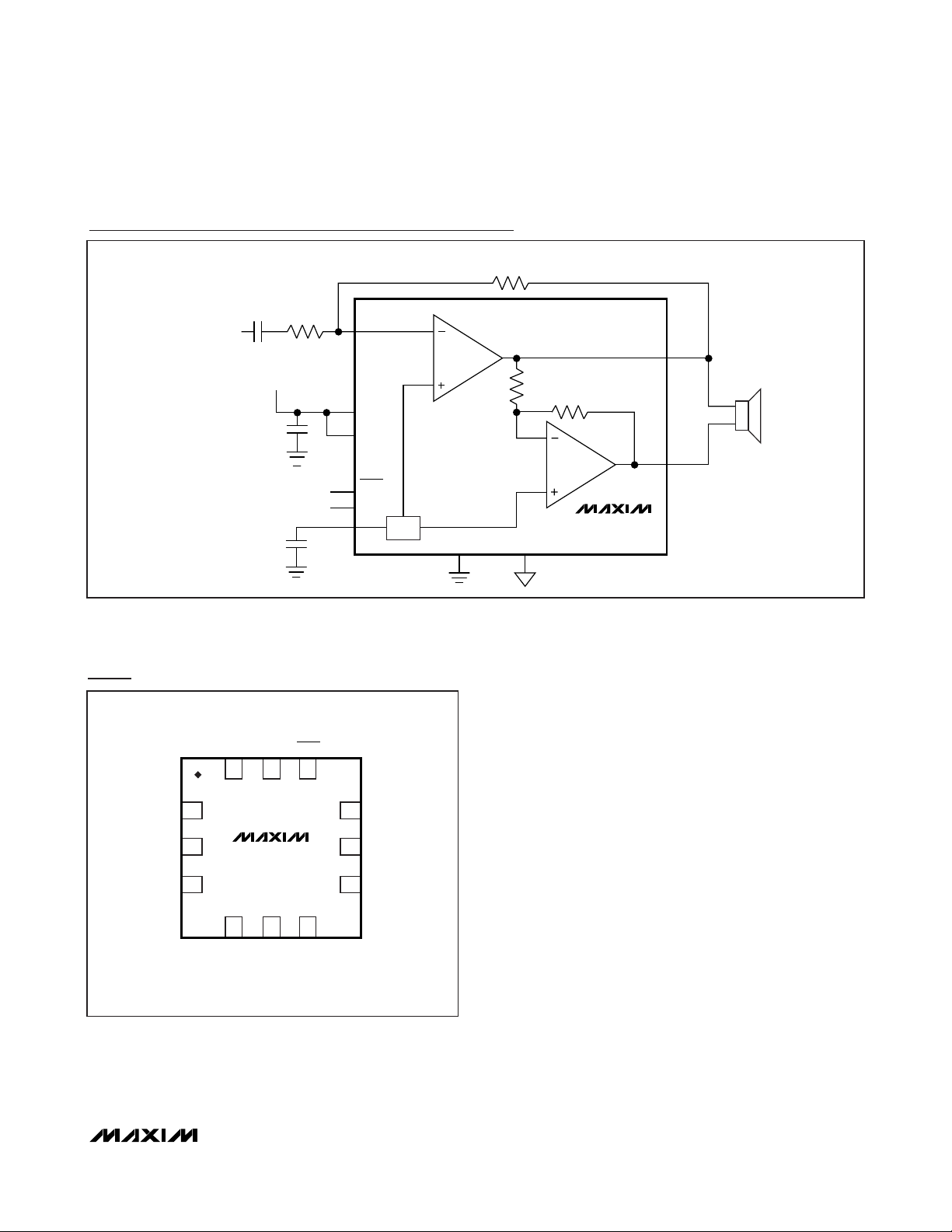
General Description
The MAX9710/MAX9711 are stereo/mono 3W bridge-tied
load (BTL) audio power amplifiers. These devices are
PC99/01 compliant, operate from a single 4.5V to 5.5V
supply, and feature an industry-leading 100dB PSRR,
which allows these devices to operate from noisy supplies without additional, costly power-supply conditioning. An ultra-low 0.005% THD+N ensures clean,
low-distortion amplification of the audio signal while
click-and-pop suppression eliminates audible transients
on power and shutdown cycles. Power-saving features
include low 2mV VOS(minimizing DC current drain
through the speakers), low 7mA supply current, and a
0.5µA shutdown mode. A MUTE function allows the outputs to be quickly enabled or disabled.
These devices include thermal overload protection, are
specified over the extended -40°C to +85°C temperature range, and are supplied in thermally efficient packages. The MAX9710 is available in a 20-pin thin QFN
package (5mm
✕ 5mm ✕ 0.8mm). The MAX9711 is
available in a 12-pin thin QFN package (4mm
✕ 4mm ✕
0.8mm).
Applications
Features
♦ 3W into 3Ω (1% THD+N)
♦ 4W into 3Ω (10% THD+N)
♦ Industry-Leading, Ultra-High 100dB PSRR
♦ PC99/01 Compliant
♦ Click-and-Pop Suppression
♦ Low 0.005% THD+N
♦ Low Quiescent Current: 7mA
♦ Low-Power Shutdown Mode: 0.5µA
♦ MUTE Function
♦ Tiny 20-Pin Thin QFN (5mm
✕ 5mm ✕ 0.8mm)
MAX9710/MAX9711
3W Mono/Stereo BTL Audio Power Amplifiers
with Shutdown
________________________________________________________________
Maxim Integrated Products
1
Ordering Information
19-2841; Rev 1; 6/08
EVALUATION KIT
AVAILABLE
PART
TEMP RANGE
PIN-PACKAGE
AMP
MAX9710ETP
Stereo
MAX9711ETC
Mono
MAX9710
TQFN
1INL
2BIAS
3N.C.
4MUTE
5INR
6
PGND
7
OUTR+
8
PV
DD
9
OUTR-
10
N.C.
11 PGND
12 V
DD
13 N.C.
14
15 PGND
16
N.C.
17
OUTL-
18
PV
DD
19
OUTL+
20
PGND
SHDN
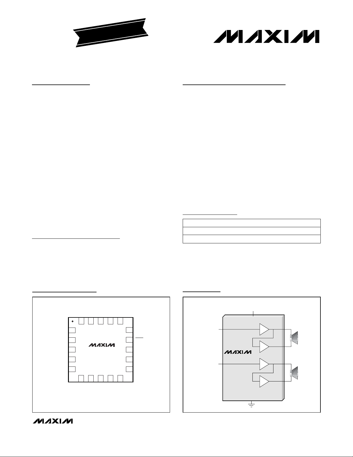
TOP VIEW
SINGLE SUPPLY
4.5V TO 5.5V
MAX9710
LEFT IN
RIGHT IN
Pin Configurations
Simplified Block Diagram
*
EP = Exposed pad.
Notebook PCs
Flat-Panel TVs
Flat-Panel PC Displays
Two-Way Radios
General-Purpose Audio
Powered Speakers
Pin Configurations continued at end of data sheet.
For pricing, delivery, and ordering information, please contact Maxim Direct at 1-888-629-4642,
or visit Maxim’s website at www.maxim-ic.com.
-40°C to +85°C
-40°C to +85°C
20-Thin QFN-EP*
12-Thin QFN-EP*
Page 2
MAX9710/MAX9711
3W Mono/Stereo BTL Audio Power Amplifiers
with Shutdown
2 _______________________________________________________________________________________
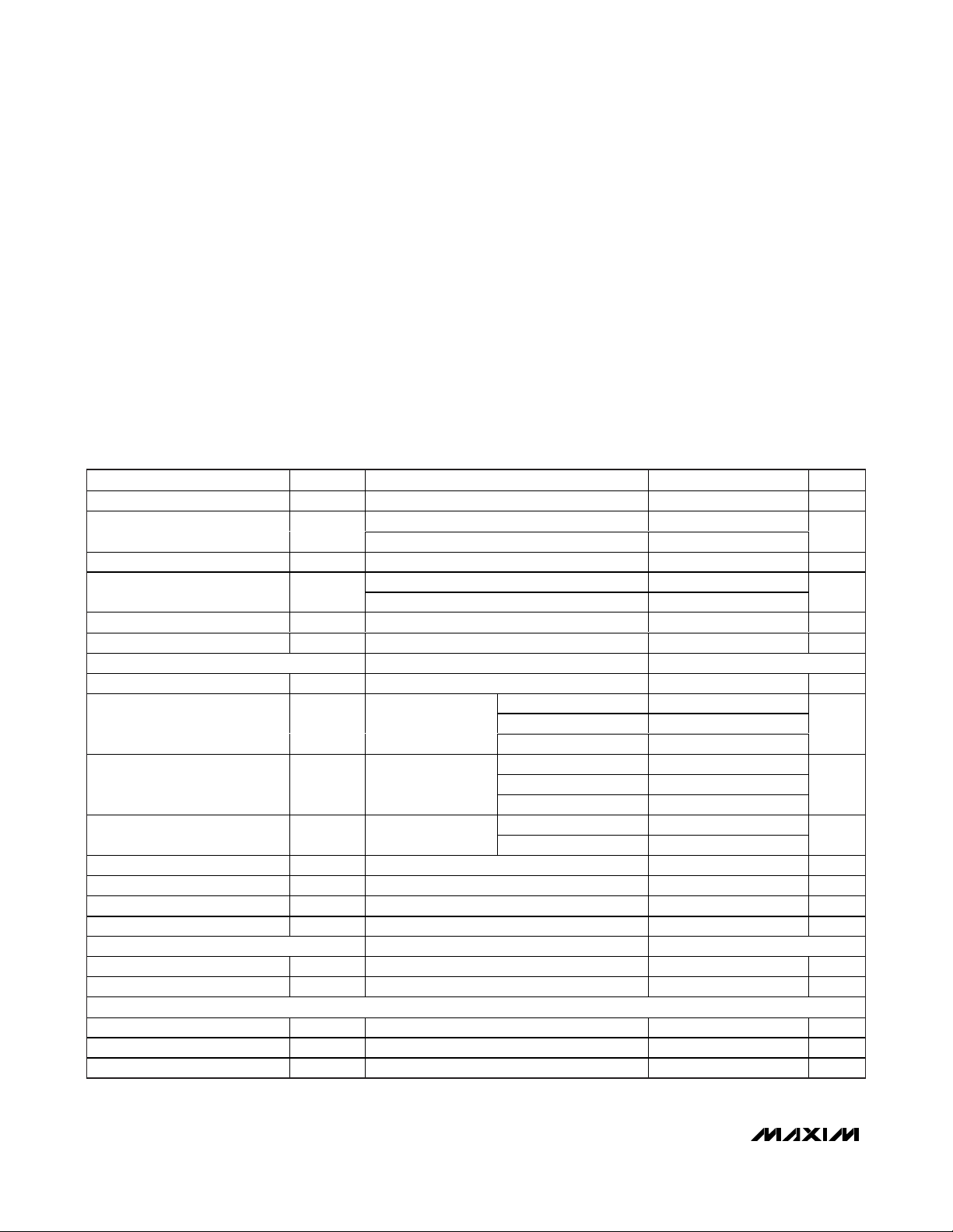
ABSOLUTE MAXIMUM RATINGS
ELECTRICAL CHARACTERISTICS
(VDD= PVDD= 5.0V, V
GND
= V
PGND
= V
MUTE
= 0V, V
SHDN
= 5V, RIN= RF= 15kΩ, RL= ∞. TA= T
MIN
to T
MAX
, unless otherwise
noted. Typical values are at T
A
= +25°C.) (Note 1)
Stresses beyond those listed under “Absolute Maximum Ratings” may cause permanent damage to the device. These are stress ratings only, and functional
operation of the device at these or any other conditions beyond those indicated in the operational sections of the specifications is not implied. Exposure to
absolute maximum rating conditions for extended periods may affect device reliability.
Note 1: All devices are 100% production tested at +25°C. All temperature limits are guaranteed by design.
Note 2: PSSR is specified with the amplifier inputs connected to GND through R
IN
and CIN.
V
DD
to GND, PGND ...............................................................+6V
PV
DD
to VDD.......................................................................±0.3V
PGND to GND.....................................................................±0.3V
All Other Pins to GND.................................-0.3V to (V
DD
+ 0.3V)
Continuous Input Current (into any pin
except power supply and output pins).........................±20mA
Continuous Power Dissipation (T
A
= +70°C)
12-Pin Thin QFN (derate 16.9mW/°C above +70°C) ....1349mW
20-Pin Thin QFN (derate 20.8mW/°C above +70°C) ....1667mW
Operating Temperature Range............................-40°C to +85°C
Storage Temperature Range .............................-65°C to +150°C
Junction Temperature ......................................................+150°C
Lead Temperature (soldering, 10s) .................................+300°C
PARAMETER SYMBOL CONDITIONS MIN TYP MAX UNITS
Supply Voltage Range VDD/PVDDInferred from PSRR test 4.5 5.5 V
Quiescent Supply Current
(I
VDD
+ I
PVDD
)
Shutdown Supply Current I
Turn-On Time t
Thermal Shutdown Threshold 160 °C
Thermal Shutdown Hysteresis 15 °C
OUTPUT AMPLIFIERS
Output Offset Voltage V
Power-Supply Rejection Ratio PSRR
Total Harmonic Distortion Plus
Noise
Signal-to-Noise Ratio SNR RL = 8Ω, V
Slew Rate SR 1.6 V/µs
Maximum Capacitive Load Drive C
Crosstalk fIN = 10kHz 77 dB
BIAS VOLTAGE (BIAS)
BIAS Voltage V
Output Resistance R
DIGITAL INPUTS (MUTE, SHDN)
Input Voltage High V
Input Voltage Low V
Input Leakage Current I
I
DD
SHDN
ON
OS
OUT
THD+N
L
BIAS
BIAS
IH
IL
IN
MAX9710 12 30
MAX9711 7 17
SHDN = GND 0.5 30 µA
C
= 1µF (10% of final value) 300
BIAS
C
= 0.1µF (10% of final value) 30
BIAS
V
V
OUT_+
RIPPLE
- V
OUT_-
= 200mV
(Note 2)
fIN = 1kHz,
THD+N < 1%
f
= 1kHz, BW =
IN
22Hz to 22kHz
OU T
No sustained oscillations 1 nF
, AV = 2 ±2 ±14 mV
VDD = 4.5V to 5.5V 82 100
P-P
f = 1kHz 87
f = 20kHz 74
RL = 8Ω 1.1 1.4
RL = 4Ω 2.6Output Power P
= 3Ω 3
R
L
P
= 1.2W, RL = 8Ω 0.005
OUT
P
= 2W, 4Ω 0.01
OUT
= 2.8V
, BW = 22H z to 22kH z95 dB
RM S
2.35 2.5 2.65 V
50 kΩ
2V
0.8 V
±1µA
mA
ms
dB
W
%
Page 3
MAX9710/MAX9711
3W Mono/Stereo BTL Audio Power Amplifiers
with Shutdown
_______________________________________________________________________________________ 3
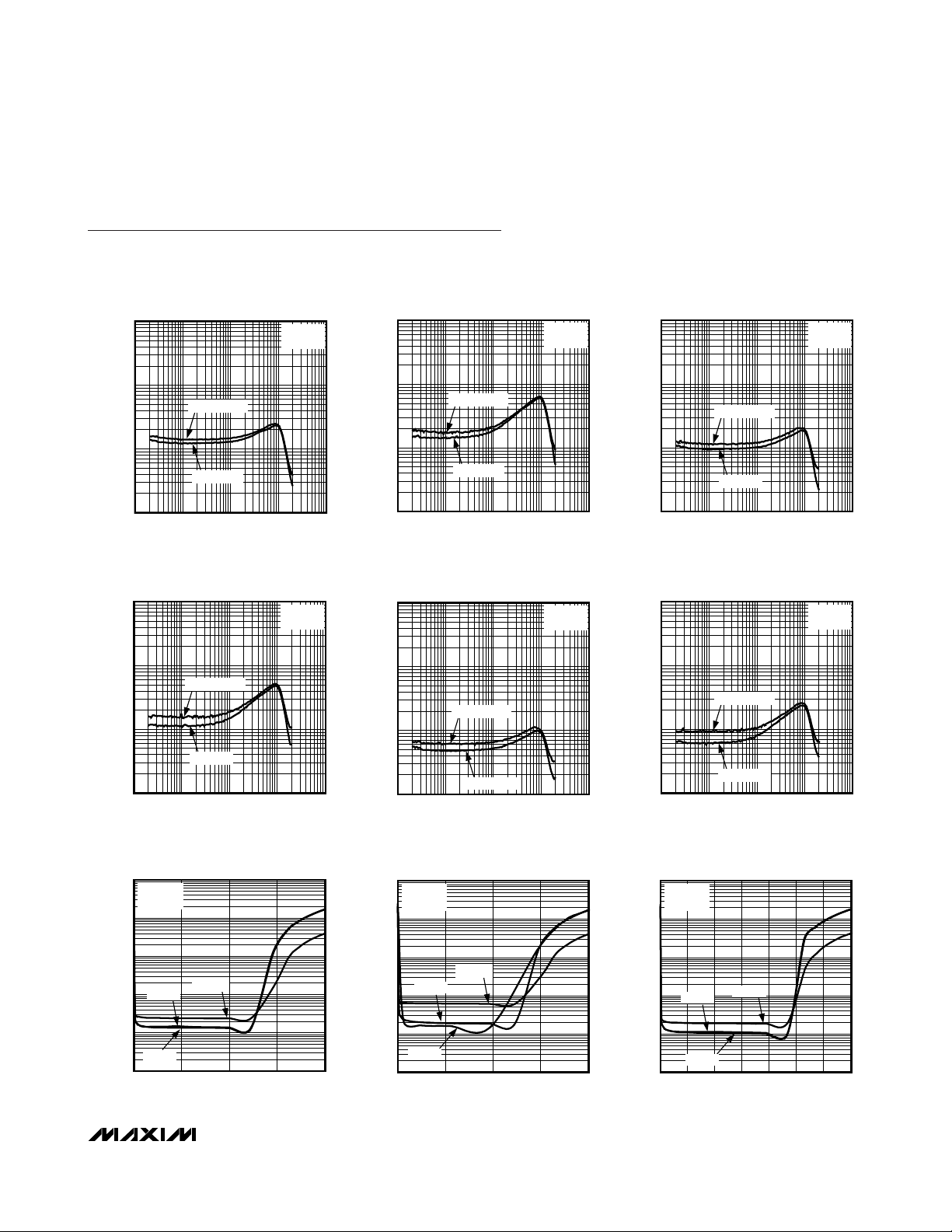
Typical Operating Characteristics
(VDD= 5V, THD+N measurement bandwidth = 22Hz to 22kHz, TA= +25°C, unless otherwise noted.)
TOTAL HARMONIC DISTORTION PLUS NOISE
vs. FREQUENCY
1
0.1
P
= 500mW
OUT
THD+N (%)
0.01
P
= 2.5W
OUT
0.001
10 100k
FREQUENCY (Hz)
10k1k100
TOTAL HARMONIC DISTORTION PLUS NOISE
vs. FREQUENCY
1
0.1
THD+N (%)
0.01
P
OUT
= 250mW
RL = 4Ω
A
RL = 3Ω
= -2V/V
A
V
= -4V/V
V
MAx9710/11 toc01
MAx9710/11 toc04
TOTAL HARMONIC DISTORTION PLUS NOISE
vs. FREQUENCY
1
0.1
THD+N (%)
0.01
0.001
10 100k
P
= 500mW
OUT
P
= 2.5W
OUT
FREQUENCY (Hz)
10k1k100
TOTAL HARMONIC DISTORTION PLUS NOISE
vs. FREQUENCY
1
0.1
P
= 250mW
THD+N (%)
0.01
OUT
RL = 3Ω
= -4V/V
A
V
RL = 8Ω
= -2V/V
A
V
MAx9710/11 toc02
MAx9710/11 toc05
TOTAL HARMONIC DISTORTION PLUS NOISE
1
0.1
THD+N (%)
0.01
0.001
TOTAL HARMONIC DISTORTION PLUS NOISE
1
0.1
THD+N (%)
0.01
vs. FREQUENCY
RL = 4Ω
= -2V/V
A
V
P
= 250mW
OUT
P
= 2W
OUT
10 100k
FREQUENCY (Hz)
10k1k100
vs. FREQUENCY
RL = 8Ω
= -4V/V
A
V
P
= 250mW
OUT
MAx9710/11 toc03
MAx9710/11 toc06
P
= 2W
OUT
0.001
10 100k
FREQUENCY (Hz)
10k1k100
TOTAL HARMONIC DISTORTION PLUS NOISE
0.001
10 100k
TOTAL HARMONIC DISTORTION PLUS NOISE
vs. OUTPUT POWER
100
AV = -2V/V
= 3Ω
R
L
10
1
THD+N (%)
0.1
0.01
f = 1kHz
0.001
04
f = 20Hz
f = 10kHz
321
OUTPUT POWER (W)
MAX9710/11 toc07
100
AV = -4V/V
= 3Ω
R
L
10
1
THD+N (%)
0.001
f = 1kHz
0.1
0.01
f = 20Hz
04
P
= 1.2W
OUT
FREQUENCY (Hz)
vs. OUTPUT POWER
f = 10kHz
OUTPUT POWER (W)
P
= 1.2W
OUT
0.001
10k1k100
10 100k
FREQUENCY (Hz)
10k1k100
TOTAL HARMONIC DISTORTION PLUS NOISE
vs. OUTPUT POWER
100
AV = -2V/V
= 4Ω
R
L
10
MAX9710/11 toc08
1
THD+N (%)
0.1
f = 1kHz
0.01
0.001
321
0 3.5
f = 10kHz
f = 20Hz
2.5 3.01.5 2.01.00.5
OUTPUT POWER (W)
MAX9710/11 toc09
Page 4
MAX9710/MAX9711
3W Mono/Stereo BTL Audio Power Amplifiers
with Shutdown
4 _______________________________________________________________________________________
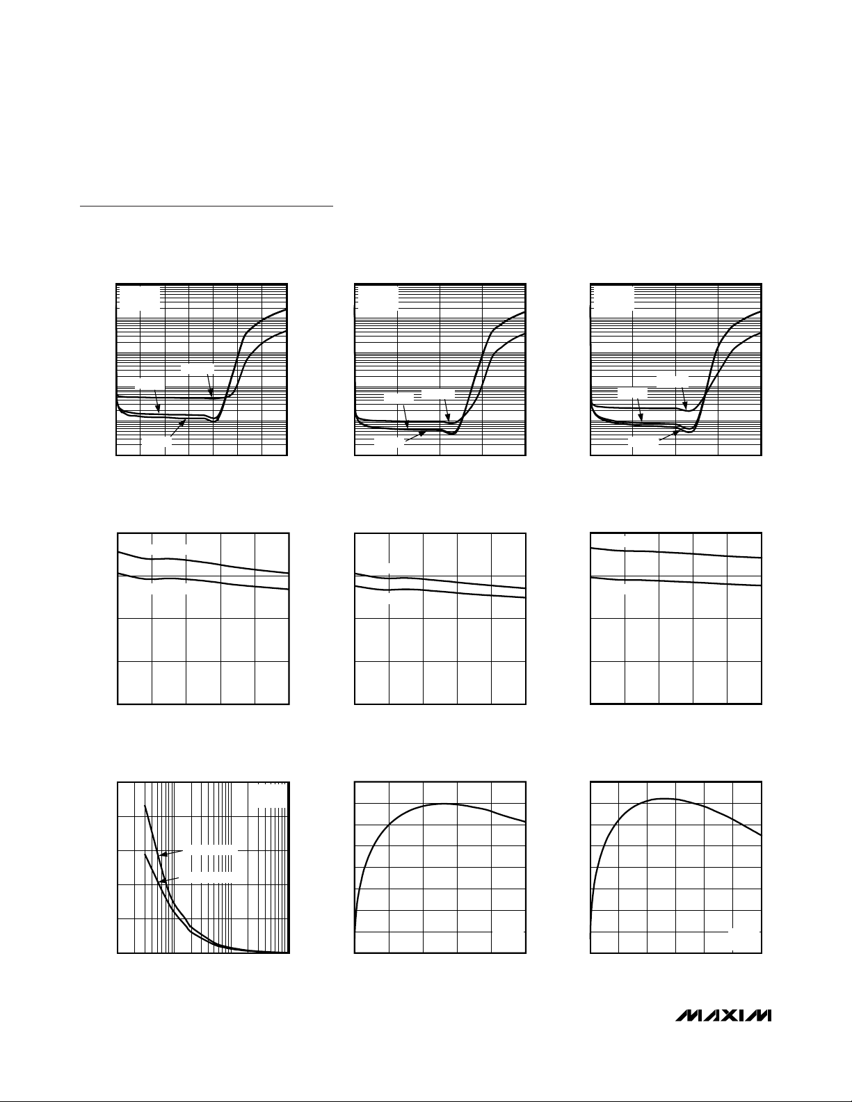
Typical Operating Characteristics (continued)
(VDD= 5V, THD+N measurement bandwidth = 22Hz to 22kHz, TA= +25°C, unless otherwise noted.)
TOTAL HARMONIC DISTORTION PLUS NOISE
vs. OUTPUT POWER
100
AV = -4V/V
= 4Ω
R
L
10
1
THD+N (%)
0.01
0.001
f = 1kHz
0.1
0 3.5
f = 10kHz
f = 20Hz
2.5 3.01.5 2.01.00.5
OUTPUT POWER (W)
MAX9710/11 toc10
THD+N (%)
0.001
OUTPUT POWER
vs. TEMPERATURE
4
THD+N = 10%
3
2
OUTPUT POWER (W)
1
0
THD+N = 1%
f = 1kHz
= 3Ω
R
L
-40 85
TEMPERATURE (°C)
603510-15
MAX9710/11 toc13
OUTPUT POWER (W)
TOTAL HARMONIC DISTORTION PLUS NOISE
vs. OUTPUT POWER
100
AV = -2V/V
= 8Ω
R
L
10
1
0.1
0.01
f = 20Hz
0
f = 10kHz
f = 1kHz
OUTPUT POWER (W)
1.5 2.01.00.5
OUTPUT POWER
vs. TEMPERATURE
4
THD+N = 10%
3
THD+N = 1%
2
1
f = 1kHz
= 4Ω
R
L
0
-40 85
TEMPERATURE (°C)
603510-15
MAX9710/11 toc11
THD+N (%)
0.001
MAX9710/11 toc14
OUTPUT POWER (W)
TOTAL HARMONIC DISTORTION PLUS NOISE
vs. OUTPUT POWER
100
AV = -4V/V
= 8Ω
R
L
10
1
0.1
0.01
0
f = 10kHz
f = 1kHz
f = 20Hz
OUTPUT POWER (W)
1.5 2.01.00.5
OUTPUT POWER
vs. TEMPERATURE
2.0
THD+N = 10%
1.5
THD+N = 1%
1.0
0.5
f = 1kHz
= 8Ω
R
L
0
-40 85
TEMPERATURE (°C)
603510-15
MAX9710/11 toc12
MAX9710/11 toc15
OUTPUT POWER vs. LOAD RESISTANCE
(FORCED-AIR COOLING)
5
4
3
2
OUTPUT POWER (W)
1
0
1 1000
THD+N = 10%
THD+N = 1%
10010
LOAD RESISTANCE (Ω)
VDD = 5V
f = 1kHz
1.6
1.4
MAX9710/11 toc16
1.2
1.0
0.8
0.6
POWER DISSIPATION (W)
0.4
0.2
0
POWER DISSIPATION
vs. OUTPUT POWER
RL = 4Ω
f = 1kHz
0 2.5
OUTPUT POWER (W)
2.01.50.5 1.0
0.8
0.7
MAX9710/11 toc17
0.6
0.5
0.4
0.3
POWER DISSIPATION (W)
0.2
0.1
0
POWER DISSIPATION
vs. OUTPUT POWER
0 1.501.25
OUTPUT POWER (W)
MAX9710/11 toc18
RL = 8Ω
f = 1kHz
1.000.750.25 0.50
Page 5
MAX9710/MAX9711
3W Mono/Stereo BTL Audio Power Amplifiers
with Shutdown
_______________________________________________________________________________________ 5
Typical Operating Characteristics (continued)
(VDD= 5V, THD+N measurement bandwidth = 22Hz to 22kHz, TA= +25°C, unless otherwise noted.)
POWER-SUPPLY REJECTION RATIO
vs. FREQUENCY
0
V
= 200mV
RIPPLE
-20
-40
PSRR (dB)
-60
-80
-100
10 100k
P-P
FREQUENCY (Hz)
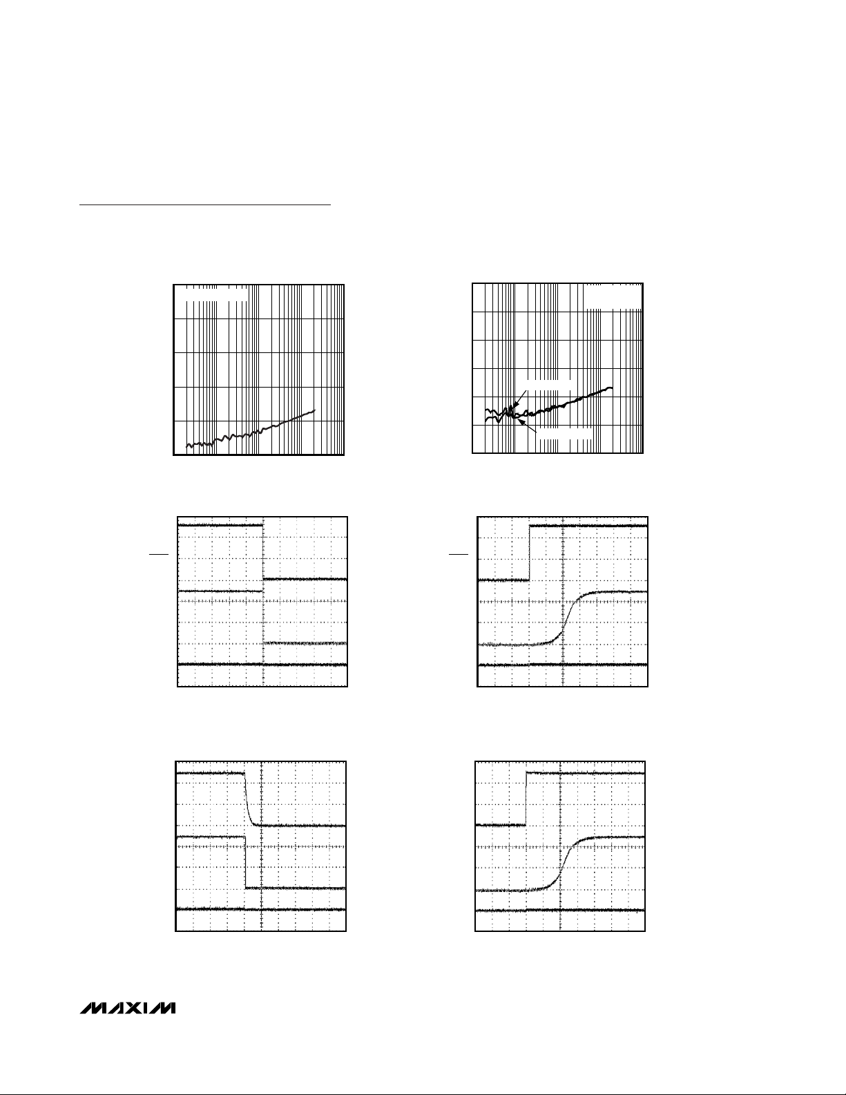
ENTERING SHUTDOWN
SHDN
10k1k100
MAX9710/11 toc21
MAX9710/11 toc19
2V/div
-20
-40
-60
CROSSTALK (dB)
-80
-100
-120
SHDN
CROSSTALK vs. FREQUENCY
0
RIGHT TO LEFT
LEFT TO RIGHT
0.01 100
FREQUENCY (Hz)
EXITING SHUTDOWN
VIN = 200mV
RL = 8Ω
1010.1
MAX9710/11 toc22
P-P
MAX9710/11 toc20
2V/div
OUT_+ AND
OUT_-
OUT_+ -
OUT_-
V
OUT_+ AND
OUT_-
OUT_+ -
OUT_-
RL = 8Ω
INPUT AC-COUPLED TO GND
ENTERING POWER-DOWN
DD
RL = 8Ω
INPUT AC-COUPLED TO GND
100ms/div
100ms/div
MAX9710/11 toc23
1V/div
200mV/div
2V/div
1V/div
200mV/div
OUT_+ AND
OUT_-
OUT_+ -
OUT_-
V
OUT_+ AND
OUT_-
OUT_+ -
OUT_-
RL = 8Ω
INPUT AC-COUPLED TO GND
EXITING POWER-DOWN
DD
RL = 8Ω
INPUT AC-COUPLED TO GND
1V/div
200mV/div
100ms/div
MAX9710/11 toc24
2V/div
1V/div
200mV/div
100ms/div
Page 6
MAX9710/MAX9711
3W Mono/Stereo BTL Audio Power Amplifiers
with Shutdown
6 _______________________________________________________________________________________
Pin Description
MAX9710
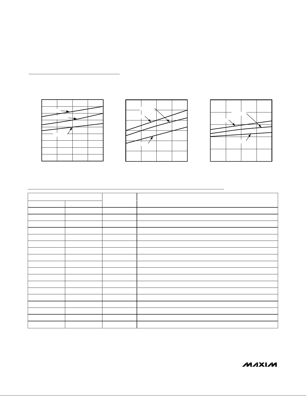
SUPPLY CURRENT vs. SUPPLY VOLTAGE
MAX9710/11 toc25
SUPPLY VOLTAGE (V)
SUPPLY CURRENT (mA)
5.255.004.75
2
4
6
8
10
12
14
16
18
0
4.50 5.50
TA = +85°C
TA = +25°C
TA = -40°C
Typical Operating Characteristics (continued)
(VDD= 5V, THD+N measurement bandwidth = 22Hz to 22kHz, TA= +25°C, unless otherwise noted.)
MAX9711
SUPPLY CURRENT vs. SUPPLY VOLTAGE
MAX9710/11 toc26
SUPPLY VOLTAGE (V)
SUPPLY CURRENT (mA)
5.255.004.75
2
4
6
8
10
12
0
4.50 5.50
TA = +85°C
TA = +25°C
TA = -40°C
SHUTDOWN SUPPLY CURRENT
vs. SUPPLY VOLTAGE
MAX9710/11 toc27
SUPPLY VOLTAGE (V)
SUPPLY CURRENT (μA)
5.255.004.75
0.2
0.4
0.6
0.8
1.0
0
4.50 5.50
TA = +85°C
TA = +25°C
TA = -40°C
MAX9710 MAX9711
1 — INL Left-Channel Input
2 7 BIAS DC Bias Bypass. See BIAS Capacitor section for capacitor selection.
3, 10, 13, 16 — N.C. No Connection. Not internally connected.
4 9 MUTE Active-High Mute Input
5 — INR Right-Channel Input
6, 11, 15, 20 1, 3 PGND Power Ground
7 — OUTR+ Right-Channel Bridged Amplifier Positive Output
8, 18 5, 11 PV
9 — OUTR- Right-Channel Bridged Amplifier Negative Output
12 8 V
14 10 SHDN Active-Low Shutdown. Connect SHDN to VDD for normal operation.
17 — OUTL- Left-Channel Bridged Amplifier Negative Output
19 — OUTL+ Left-Channel Bridged Amplifier Positive Output
— 2 IN Amplifier Input
— 6 GND Ground
— 12 OUT- Bridged Amplifier Negative Output
— 4 OUT+ Bridged Amplifier Positive Output
— — EP Exposed Pad. Connect to ground plane.
PIN
NAME FUNCTION
DD
DD
Output Amplifier Power Supply
Power Supply
Page 7
Detailed Description
The MAX9710/MAX9711 are 3W BTL speaker amplifiers. The MAX9710 is a stereo speaker amplifier, while
the MAX9711 is a mono speaker amplifier. Both
devices feature a low-power shutdown mode, MUTE
mode, and comprehensive click-and-pop suppression.
These devices consist of high output-current op amps
configured as BTL amplifiers (see
Functional
Diagrams
). The device gain is set by RFand RIN.
BIAS
These devices operate from a single 5V supply and
feature an internally generated, power-supply-independent, common-mode bias voltage of 2.5V referenced to
ground. BIAS provides both click-and-pop suppression
and sets the DC bias level for the audio outputs. BIAS
is internally connected to the noninverting input of each
speaker amplifier (see
Functional Diagrams
). Choose
the value of the bypass capacitor as described in the
BIAS Capacitor
section. No external load should be
applied to BIAS. Any load lowers the BIAS voltage,
affecting the overall performance of the device.
Shutdown
The MAX9710/MAX9711 feature a 0.5µA low-power shutdown mode that reduces quiescent current consumption. Pulling SHDN low disables the device’s bias
circuitry, the amplifier outputs are actively pulled low,
and BIAS is driven to GND. Connect SHDN to VDDfor
normal operation.
MUTE
Both devices feature a clickless/popless MUTE mode.
When the device is muted, the input disconnects from
the amplifier. MUTE only affects the power amplifiers
and does not shut down the device. Drive MUTE high to
mute the device. Drive MUTE low for normal operation.
Click-and-Pop Suppression
The MAX9710/MAX9711 feature Maxim’s comprehensive click-and-pop suppression. During startup, the
common-mode bias voltage of the amplifiers slowly
ramps to the DC bias point using an S-shaped waveform. When entering shutdown, the amplifier outputs are
actively driven low simultaneously. This scheme minimizes the energy present in the audio band.
For optimum click-and-pop suppression, choose:
RINx CIN< R
BIAS
x C
BIAS
where R
BIAS
= 50kΩ.
Applications Information
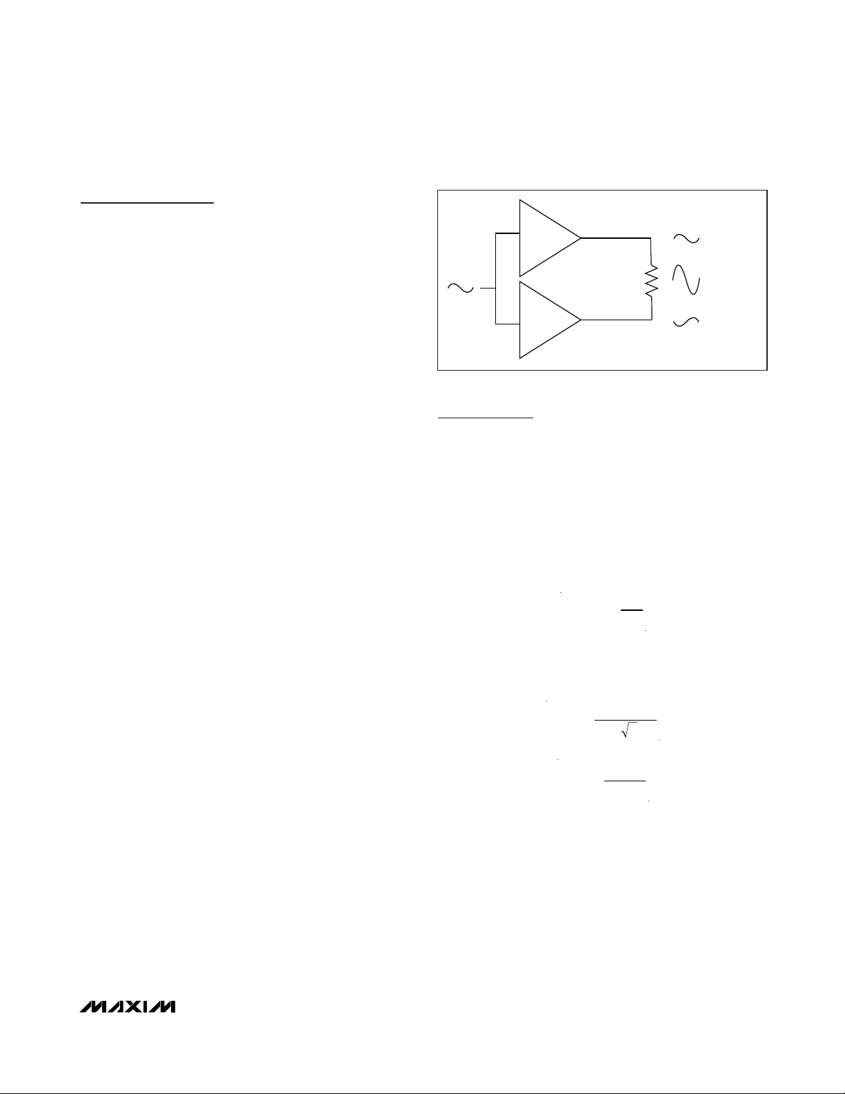
BTL Amplifier
The MAX9710/MAX9711 are designed to drive a load
differentially, a configuration referred to as BTL. The
BTL configuration (Figure 1) offers advantages over the
single-ended configuration, where one side of the load
is connected to ground. Driving the load differentially
doubles the output voltage compared to a singleended amplifier under similar conditions. Thus, the differential gain of the device is twice the closed-loop gain
of the input amplifier. The effective gain is given by:
Substituting 2 x V
OUT(P-P)
for V
OUT(P-P)
into the following equations yields four times the output power due to
doubling of the output voltage:
Since the differential outputs are biased at midsupply,
there is no net DC voltage across the load. This eliminates the need for DC-blocking capacitors required for
single-ended amplifiers. These capacitors can be
large, expensive, consume board space, and degrade
low-frequency performance.
P
V
R
OUT
RMS
L
=
2
V
V
RMS
OUT P P
=
−()
22
A
R
R
VD
F
IN
=×2
MAX9710/MAX9711
3W Mono/Stereo BTL Audio Power Amplifiers
with Shutdown
_______________________________________________________________________________________ 7
+1
V
OUT(P-P)
2 x V
OUT(P-P)
V
OUT(P-P)
-1
Figure 1. Bridge-Tied Load Configuration
Page 8

MAX9710/MAX9711
Power Dissipation and Heat Sinking
Under normal operating conditions, the MAX9710/
MAX9711 dissipate a significant amount of power. The
maximum power dissipation for each package is given
in the
Absolute Maximum Ratings
section under
Continuous Power Dissipation or can be calculated by
the following equation:
where T
J(MAX
) is +150°C, TAis the ambient temperature,
and θ
JA
is the reciprocal of the derating factor in °C/W as
specified in the
Absolute Maximum Ratings
section. For
example, θJAof the 20-pin thin QFN package is
48.1°C/W.
The increase in power delivered by the BTL configuration directly results in an increase in internal power dissipation over the single-ended configuration. The
maximum power dissipation for a given V
DD
and load is
given by the following equation:
If the power dissipation for a given application exceeds
the maximum allowed for a given package, either reduce
VDD, increase load impedance, decrease the ambient
temperature, or add heat sinking to the device (see
Layout and Grounding
section). Large output, supply,
and ground PC board traces improve the maximum
power dissipation in the package.
Thermal-overload protection limits total power dissipation in the MAX9710/MAX9711. When the junction
temperature exceeds +160°C, the thermal protection
circuitry disables the amplifier output stage. The
amplifiers are enabled once the junction temperature
cools by 15°C. A pulsing output under continuous
thermal-overload conditions results as the device heats
and cools.
Component Selection
Gain-Setting Resistors
External feedback components set the gain of both
devices. Resistors RFand RIN(
Functional Diagrams
)
set the gain of the amplifier as follows:
Input Filter
The input capacitor (CIN), in conjunction with RIN, forms
a highpass filter that removes the DC bias from an
incoming signal. The AC-coupling capacitor allows the
amplifier to bias the signal to an optimum DC level.
Assuming zero-source impedance, the -3dB point of
the highpass filter is given by:
For optimum click-and-pop suppression, choose:
RINx CIN< R
BIAS
x C
BIAS
where R
BIAS
= 50kΩ.
Setting f
-3dB
too high affects the low-frequency
response of the amplifier. Use capacitors with
dielectrics that have low-voltage coefficients, such as
tantalum or aluminum electrolytic. Capacitors with highvoltage coefficients, such as ceramics, may result in an
increase of distortion at low frequencies.
BIAS Capacitor
BIAS is the output of the internally generated 2.5VDC
bias voltage. The BIAS bypass capacitor, C
BIAS
,
improves PSRR and THD+N by reducing power supply
and other noise sources at the common-mode bias
node, and also generates the clickless/popless startup
DC bias waveform for the speaker amplifiers. Bypass
BIAS with a 1µF capacitor to GND. Smaller values of
C
BIAS
produce faster tON/t
OFF
times but may result in
increased click/pop levels.
Supply Bypassing
Proper power-supply bypassing ensures low-noise,
low-distortion performance. Place a 0.1µF ceramic
capacitor from V
DD
to PGND. Add additional bulk
capacitance as required by the application. Locate the
bypass capacitor as close to the device as possible.
Piezoelectric Speaker Driver
Low-profile piezoelectric speakers can provide quality
sound for portable electronics. However, piezoelectric
speakers typically require large voltage swings
(>8V
P-P
) across the speaker element to produce
audible sound pressure levels. The MAX9711 can be
configured to drive a piezoelectric speaker with up to
10V
P-P
while operating from a single 5V supply.
Figure 2 shows the THD+N of the MAX9711 driving a
piezoelectric speaker. Note that as frequency increases, the THD+N increases. This is due to the capacitive
nature of the piezoelectric speaker; as frequency
increases, the speaker impedance decreases, resulting
in a larger current draw from the amplifier.
f
RC
dB
IN IN
−
=
3
1
2π
A
R
R
VD
F
IN
=×2
P
V
R
DISS MAX
DD
L
()
=
2
2
2
π
P
TT
DISSPKG MAX
J MAX A
JA
()
()
=
−
θ
3W Mono/Stereo BTL Audio Power Amplifiers
with Shutdown
8 _______________________________________________________________________________________
Page 9
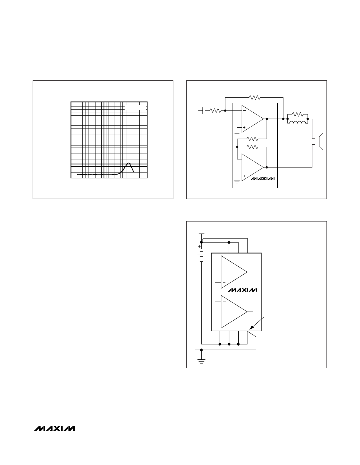
The capacitive nature of the piezoelectric speaker may
cause the MAX9711 to become unstable. A simple inductor/resistor network in series with the speaker isolates the
speaker capacitance from the driver and ensures that the
device output sees a resistive load of about 10Ω at high
frequency, thereby maintaining stability (Figure 3).
Layout and Grounding
Good PC board layout is essential for optimizing performance. Use large traces for the power-supply inputs and
amplifier outputs to minimize losses due to parasitic
trace resistance and route heat away from the device.
Good grounding improves audio performance,
minimizes crosstalk between channels, and prevents any
digital switching noise from coupling into the audio
signal.
The MAX9710/MAX9711 thin QFN package features an
exposed thermal pad on the underside. This pad lowers the thermal resistance of the package by providing
a direct-heat conduction path from the die to the printed circuit board. Connect the exposed pad to the
ground plane using multiple vias, if required. For optimum performance, connect to the ground planes as
shown in Figure 4.
MAX9710/MAX9711
3W Mono/Stereo BTL Audio Power Amplifiers
with Shutdown
_______________________________________________________________________________________ 9
Figure 2. MAX9711 Piezoelectric Speaker Driver THD+N vs.
Frequency
Figure 3. Isolation Network for Driving a Piezoelectric Speaker
Figure 4. MAX9710 Audio Ground Connection
TOTAL HARMONIC DISTORTI0N PLUS NOISE
vs. FREQUENCY
10
1
V
= 8V
OUT
1μF
P-P
AUDIO
INPUT
15kΩ
2
15kΩ
IN
OUT+
10Ω
4
100μH
0.1
THD+N (%)
0.01
0.001
0.01 100
FREQUENCY (Hz)
1010.1
*
12
OUT-
MAX9711
*PIEZOELECTRIC
SPEAKER.
5V
PV
DD
V
DD
MAX9710
FOR OPTIMUM PERFORMANCE,
AUDIO GND SHOULD HAVE A
STAR CONNECTION TO THE HIGH
CURRENT, AMPLIFIER PGND AT
A SINGLE POINT, PIN 6.
PGND
AUDIO SIGNAL
GND
Page 10

MAX9710/MAX9711
3W Mono/Stereo BTL Audio Power Amplifiers
with Shutdown
10 ______________________________________________________________________________________
Functional Diagrams
R
F
15kΩ
C
IN
R
LEFT AUDIO
INPUT
0.1μF
15kΩ
IN
1
INL
19
OUTL+
4.5V TO 5.5V
SUPPLY
V
12
DD
PV
0.1μF
C
BIAS
RIGHT AUDIO
INPUT
1μF
C
0.1μF
6, 11, 15, 20
IN
R
IN
15kΩ
2,18
DD
BIAS
2
PGND
SHDN
14
MUTE
4
5
INR
BIAS
10kΩ
10kΩ
R
15kΩ
F
10kΩ
10kΩ
MAX9710
OUTL-
OUTR-
OUTR+
17
9
7
PIN NUMBERS SHOWN ARE FOR THE 20 TQFN-EP PACKAGE.
Page 11
MAX9710/MAX9711
3W Mono/Stereo BTL Audio Power Amplifiers
with Shutdown
______________________________________________________________________________________ 11
Functional Diagrams (continued)
Pin Configurations (continued)
LEFT AUDIO
INPUT
C
IN
0.1μF
4.5V TO 5.5V
SUPPLY
0.1μF
C
BIAS
1μF
R
15kΩ
R
F
15kΩ
IN
2
IN
OUT+
4
10kΩ
10kΩ
MAX9711
OUT-
12
5,11
V
8
DD
PV
DD
SHDN
10
MUTE
9
BIAS
7
BIAS
GND PGND
6 1, 3
TOP VIEW
PGND
1
2IN
3
OUT-11PV
12
MAX9711
45
OUT+
PV
DD
QFN
SHDN
DD
10
9
MUTE
8
V
DD
BIAS
7PGND
6
GND
Page 12

MAX9710/MAX9711
3W Mono/Stereo BTL Audio Power Amplifiers
with Shutdown
12 ______________________________________________________________________________________
Chip Information
MAX9710 TRANSISTOR COUNT: 1172
MAX9711 TRANSISTOR COUNT: 780
PROCESS: BiCMOS
System Diagram
Package Information
For the latest package outline information and land patterns, go
to www.maxim-ic.com/packages
.
PACKAGE TYPE PACKAGE CODE DOCUMENT NO.
20 TQFN-EP T2055-4
21-0140
12 TQFN-EP T1244-4
21-0139
(5V)
V
DD
0.1μF
15kΩ
0.1μF
0.1μF
AUX_IN
1μF
OUT
MAX4060
2.2kΩ
BIAS
0.1μF
IN+
IN-
0.1μF
CODEC
V
CC
(3.3V)
1μF
0.1μF
1μF
1μF
1μF
15kΩ
15kΩ
SHDNL
SHDNR
INL
INR
V
CC
INR
V
DD
PV
DD
MUTE
BIAS
SHDN
INL
Q
MAX961
Q
MAX4411
C1P CIN
MAX9710
15kΩ
OUTL
OUTR
PV
SS
SV
SS
OUTR+
OUTR-
OUTL-
OUTL+
IN-
IN+
0.1μF
1μF
V
DD
100kΩ
V
CC
/2
100kΩ
1μF
Page 13

MAX9710/MAX9711
3W Mono/Stereo BTL Audio Power Amplifiers
with Shutdown
Revision History
Maxim cannot assume responsibility for use of any circuitry other than circuitry entirely embodied in a Maxim product. No circuit patent licenses are
implied. Maxim reserves the right to change the circuitry and specifications without notice at any time.
Maxim Integrated Products, 120 San Gabriel Drive, Sunnyvale, CA 94086 408-737-7600 ____________________
13
© 2008 Maxim Integrated Products is a registered trademark of Maxim Integrated Products, Inc.
REVISION
NUMBER
0 4/03 Initial release —
1 6/08 Removed TSSOP package 1, 2, 6, 9, 10
REVISION
DATE
DESCRIPTION
PAGES
CHANGED
 Loading...